digital communication analyzer (dca), measure relative ...1 digital communication analyzer (dca),...
TRANSCRIPT
1
Digital Communication Analyzer (DCA),Measure Relative Intensity Noise (RIN) Product Note 86100-7

2
Table of Content0. Introduction . . . . . . . . . . . . . . . . . . . . . . . . . . . . . . . . . . . . . . . . . . . . . . . . . . . . . . . . . . . . . . . . . . . . . . . . . . . . . . . . . . . . . . 31. Laser Intensity Fluctuations . . . . . . . . . . . . . . . . . . . . . . . . . . . . . . . . . . . . . . . . . . . . . . . . . . . . . . . . . . . . . . . . . . . . . . . . 42. Oscilloscope Based Measurements . . . . . . . . . . . . . . . . . . . . . . . . . . . . . . . . . . . . . . . . . . . . . . . . . . . . . . . . . . . . . . . . . . . 7 2.1. Block diagram . . . . . . . . . . . . . . . . . . . . . . . . . . . . . . . . . . . . . . . . . . . . . . . . . . . . . . . . . . . . . . . . . . . . . . . . . . . . . 7 2.2. Measurement procedure . . . . . . . . . . . . . . . . . . . . . . . . . . . . . . . . . . . . . . . . . . . . . . . . . . . . . . . . . . . . . . . . . . . . 8 2.3. Setups using square-wave patterns . . . . . . . . . . . . . . . . . . . . . . . . . . . . . . . . . . . . . . . . . . . . . . . . . . . . . . . . . . 12 2.4. RIN calculations . . . . . . . . . . . . . . . . . . . . . . . . . . . . . . . . . . . . . . . . . . . . . . . . . . . . . . . . . . . . . . . . . . . . . . . . . . 133. RF Power Meter Based Measurements . . . . . . . . . . . . . . . . . . . . . . . . . . . . . . . . . . . . . . . . . . . . . . . . . . . . . . . . . . . . . . . 15 3.1. Block diagram . . . . . . . . . . . . . . . . . . . . . . . . . . . . . . . . . . . . . . . . . . . . . . . . . . . . . . . . . . . . . . . . . . . . . . . . . . . . 15 3.2. Measurement procedure . . . . . . . . . . . . . . . . . . . . . . . . . . . . . . . . . . . . . . . . . . . . . . . . . . . . . . . . . . . . . . . . . . . 15 3.3. RIN calculations . . . . . . . . . . . . . . . . . . . . . . . . . . . . . . . . . . . . . . . . . . . . . . . . . . . . . . . . . . . . . . . . . . . . . . . . . . 164. Electrical Spectrum Analyzer Based Measurements. . . . . . . . . . . . . . . . . . . . . . . . . . . . . . . . . . . . . . . . . . . . . . . . . . . . 17 4.1. Block diagram . . . . . . . . . . . . . . . . . . . . . . . . . . . . . . . . . . . . . . . . . . . . . . . . . . . . . . . . . . . . . . . . . . . . . . . . . . . . 17 4.2. Alternative setups. . . . . . . . . . . . . . . . . . . . . . . . . . . . . . . . . . . . . . . . . . . . . . . . . . . . . . . . . . . . . . . . . . . . . . . . . 17 4.3. Measurement procedure . . . . . . . . . . . . . . . . . . . . . . . . . . . . . . . . . . . . . . . . . . . . . . . . . . . . . . . . . . . . . . . . . . . 18 4.4. RIN calculations . . . . . . . . . . . . . . . . . . . . . . . . . . . . . . . . . . . . . . . . . . . . . . . . . . . . . . . . . . . . . . . . . . . . . . . . . . 185. Optical Spectrum Analyzer Based Measurements. . . . . . . . . . . . . . . . . . . . . . . . . . . . . . . . . . . . . . . . . . . . . . . . . . . . . . 19 5.1. Block diagram . . . . . . . . . . . . . . . . . . . . . . . . . . . . . . . . . . . . . . . . . . . . . . . . . . . . . . . . . . . . . . . . . . . . . . . . . . . . 19 5.2. Measurement procedure . . . . . . . . . . . . . . . . . . . . . . . . . . . . . . . . . . . . . . . . . . . . . . . . . . . . . . . . . . . . . . . . . . . 20 5.3. RIN calculations . . . . . . . . . . . . . . . . . . . . . . . . . . . . . . . . . . . . . . . . . . . . . . . . . . . . . . . . . . . . . . . . . . . . . . . . . . 206. RIN Measurement Comparisons . . . . . . . . . . . . . . . . . . . . . . . . . . . . . . . . . . . . . . . . . . . . . . . . . . . . . . . . . . . . . . . . . . . . 21 6.1. Adjustable RIN source . . . . . . . . . . . . . . . . . . . . . . . . . . . . . . . . . . . . . . . . . . . . . . . . . . . . . . . . . . . . . . . . . . . . . 21 6.2. DCA-J versus OSA comparison using the adjustable RIN source . . . . . . . . . . . . . . . . . . . . . . . . . . . . . . . . . . 22 6.3. DCA-J versus ESA comparison using an EML Source . . . . . . . . . . . . . . . . . . . . . . . . . . . . . . . . . . . . . . . . . . . 237. Appendix . . . . . . . . . . . . . . . . . . . . . . . . . . . . . . . . . . . . . . . . . . . . . . . . . . . . . . . . . . . . . . . . . . . . . . . . . . . . . . . . . . . . . . . 25 7.1. Definitions and electrical-optical relationships . . . . . . . . . . . . . . . . . . . . . . . . . . . . . . . . . . . . . . . . . . . . . . . . 25 7.1.1. Photodetector terminology . . . . . . . . . . . . . . . . . . . . . . . . . . . . . . . . . . . . . . . . . . . . . . . . . . . . . . . . . . . . . . . . . 25 7.1.2. Laser source terminology . . . . . . . . . . . . . . . . . . . . . . . . . . . . . . . . . . . . . . . . . . . . . . . . . . . . . . . . . . . . . . . . . . 25 7.1.3. Modulation terminology. . . . . . . . . . . . . . . . . . . . . . . . . . . . . . . . . . . . . . . . . . . . . . . . . . . . . . . . . . . . . . . . . . . . 26 7.1.4. Noise terms . . . . . . . . . . . . . . . . . . . . . . . . . . . . . . . . . . . . . . . . . . . . . . . . . . . . . . . . . . . . . . . . . . . . . . . . . . . . . . 27 7.1.5. Conversions . . . . . . . . . . . . . . . . . . . . . . . . . . . . . . . . . . . . . . . . . . . . . . . . . . . . . . . . . . . . . . . . . . . . . . . . . . . . . . 30 7.2. Physical constants . . . . . . . . . . . . . . . . . . . . . . . . . . . . . . . . . . . . . . . . . . . . . . . . . . . . . . . . . . . . . . . . . . . . . . . . 31
2

3
0. Introduction Laser intensity noise can be one of the limiting factors in the transmission of analog or digital signals. It can reduce the signal-to-noise ratio and increase the bit error rate, therefore degrading system performance. Laser intensity noise can vary significantly depending on the properties of the laser, back reflections, and optical or electrical filters after the optical/electrical (O/E) conversion. In order to optimize communication links it is essential to accurately characterize the laser intensity noise, compare it with the signal strength, and if necessary allow an appropriate power budget.
Chapter 1 provides some background on laser intensity noise and how it affects the noise of the received signal. It also explains common Relative Intensity Noise (RIN) definitions.
Chapter 2 looks at the specifics of how the Agilent 86100C Infiniium DCA acquires data and characterizes RIN. It also describes the exact sequence of steps and keystrokes for manual operation and lists useful hints and caveats for typical measurement situations.
Chapters 3, 4 and 5 show alternative RIN measurements based on RF power meters (IEEE 802.3ae method), electrical spectrum analyzers (Agilent 71400C LSA method), and optical spectrum analyzers (Agilent 86142A OSA method).
Chapter 6 compares actual measurements using the different methods and discusses potential challenges and limitations.
The appendix contains a collection of formulas, conversion tables and physical constants that the reader might find useful when measuring RIN and other parameters.
3

4
In a receiver, laser intensity fluctuations can create noise that exceeds the thermal noise of the load impedance and/or the shot noise of the photodetector. It therefore can become a limiting factor for the power budget of an optical link. If so, then careful characterization of such fluctuations becomes essential to optimize system performance.
Intensity fluctuations come primarily from the spectral properties of a laser. At very low power levels a laser emits mostly spontaneous emission which, similar to the light coming from an LED, covers a range of wavelengths. Above its lasing threshold, a laser emits mostly stimulated emission and only a small amount of spontaneous emission1. The stimulated emission is concentrated at or around one wavelength and contains most of the power used for sending information along an optical fiber (Figure 1). In a photodetector the stimulated emission interacts with any residual spontaneous emission, effectively creating noise that can be observed electrically.
Most photodetectors create an output current that is proportional to the optical power which in turn is proportional to the square of the electrical field. Because of this nonlinear relationship between optical field strength and photodetector current, photons with different optical frequencies create "beat signals" similar to the process happening in electrical nonlinear devices with multiple signals at their input (for example, the mixer in a radio).
The stimulated emission (i.e., signal) in Figure 1 "beats" with the spontaneous emission right under it2, and the spontaneous emission beats with itself. However, with today's semiconductor lasers and in the absence of optical amplifiers the spontaneous-spontaneous beat noise is much smaller than the stimulated-spontaneous beat noise and usually can be ignored.
The amount of beat noise generated in the photodetector depends on the receiver's properties, particularly its bandwidth, and it matters only if it exceeds the noise in the electronics. Therefore it makes more sense to characterize the effects of laser intensity fluctuations on the electrical signal after the optical/electrical (O/E) conversion.
Relative Intensity Noise (RIN) describes the contributions of the laser intensity fluctuations to the electrical noise in the receiver relative to the signal power observed electrically. In general, RIN is normalized to a 1 Hz bandwidth so that it becomes easier to compare laser intensity fluctuations when using receivers with different bandwidths.
4
1. Laser Intensity Fluctuations
Figure 1: Distributed feedback (DFB) laser spectrum
1 The threshold is defined as the power above which the stimulated emission exceeds the spontaneous emission.2 The frequency of the beat signal found in the photocurrent is the difference between the optical frequencies of the photons.

5
The traditional definition of RIN (measured in 1/Hz or dB [1 Hz]) is the ratio of the noise power N normalized to a 1 Hz bandwidth, and the average power PI of the photocurrent – both observed electrically in the load impedance seen by the photodetector. This definition of RIN requires either an unmodulated laser, or an instrument that can accurately measure both N and PI within the modulation pattern, such as the Agilent 86100C Infiniium DCA-J.
Equation 1
N Electrical noise power (observed in the load impedance)PI Photo current power (observed in the load impedance)BN Noise bandwidth
IEEE 802.3ae defines RIN OMA (1/Hz or dB [1Hz]) as the ratio of the electrically observed noise power N normalized to a 1 Hz bandwidth and the electrical power PMOD of a square wave modulation dissipated in the load:
Equation 2
Navg Average electrical noise power (observed in the load impedance)PMOD Modulation power (observed in the load impedance)BN Noise bandwidth
If the average optical power remains the same and if the extinction ratio is very high then both definitions yield approximately the same result. The 86100C Infiniium DCA-J can measure RIN OMA as well as RIN for the "1" level. In the latter case, the DCA-J result is equivalent to the RIN of an unmodulated laser with the optical power of the "1" level. For high extinction ratios this level is almost 3 dB above the average optical power of the modulated signal.
5
)(log*10* 10 RINRIN
BPNRIN dB
NI
==
)(log*10* 10 OMARINOMARIN
BPN
OMARIN dBNMOD
avg ==

66
Figure 2 illustrates the conceptual differences between RIN and RIN OMA: RIN measurements occur on unmodulated signals, and therefore relate the electrical noise power N caused by the noise current in the load to the signal power dissipated in the load. RIN OMA measurements occur on modulated signal, and they relate the average electrical noise power to the electrical power of the modulation.
The electrical noise on the "1" level of a modulated signal is the same as the noise observed on an unmodulated signal with the same power as the "1" level. Due to its advanced triggering the 86100C can separate the power and noise levels between the "1"s and "0"s. It therefore can measure RIN as well as RIN OMA.
P (opt ) P 1(opt)
P avg
00
P unm
odul
ated
P 0(opt)
OMA
INoise INoise
Figure 2: Conceptual difference between RIN (left) and RIN OMA (right) (Top: optical signal, bottom: noise current)

7
The Agilent 86100C Infiniium DCA-J is a sampling oscilloscope with advanced trigger and pattern lock capabilities. It allows amplitude measurements in the traditional oscilloscope mode, such as optical modulation amplitude on square wave patterns (Figure 3). In Jitter Mode it can lock onto patterns that are up to 216 bits long and then separate random effects from interference. It can therefore accurately measure RIN on a variety of patterns, including square waves and industry-standard PRBS patterns.
In order to measure RIN, the oscilloscope-based method needs a digitally modulated signal. A pattern generator running at the nominal bit rate modulates the device under test (DUT). In order to see the worst-case intensity fluctuations due to reflections back to the DUT, use a polarization controller, optical power splitter, and a reflector (these components are optional if the target system has excellent return loss values).
7
2. Oscilloscope Based Measurements
2.1. Block diagram
DUT
Polarizationcontroller Single-mode
coupler
86100CInfiniium DCA-J
Adjustablereflector
Square wave or0000011111 orPRBS source
Figure 4: Agilent 86100C Infiniium DCA-J based setup3
3 Requires firmware revision 7.0 or higher and Options 001, 200, 300
Figure 3: OMA measurement on a square-wave signal

8
Figure 6: Trigger setup for trigger signals > 3.2 GHz4
8
2.2. Measurement procedure
In order to separate random noise from distortions such as overshoot, ringing, or inter-symbol interference the pattern should be either a sequence of at least five "0"s followed by the same amount of "1"s (effectively a square wave), or a PRBS pattern such as 27–1 to 210–1. Longer patterns (up to 216–1) will work as well. However, they usually increase the measurement time without noticeably changing the RIN result.
The Agilent 86100C Infiniium DCA-J can detect subsequent "1"s and "0"s in any pattern and therefore measure random fluctuations in the middle of such a sequence (see Figure 5). Leading and trailing bits of the same value help to separate inter-symbol interference and other pattern-dependent issues from the sampling point.
We'll take advantage of this feature so that we accurately measure only the random noise on the "1" and "0" levels (as well as the "1" and "0" powers) before calculating RIN or RIN OMA.
• If simulating reflections is important then substitute the DUT in Figure 4 with an Agilent 8161xA Return Loss Meter and adjust the reflection to the worst case allowed in the intended transmission system.• Connect the DUT (laser/transceiver) and turn the modulation on. Use a PRBS pattern such as 2N–1 (N = 7 to 16), or a square wave consisting of at least five "0"s followed by the same number of "1"s (see section 2.3 for details).• Verify that the DCA-J receives a good signal: press DEFAULT SETUP, then OSCILLOSCOPE MODE and finally AUTOSCALE. The instrument will warn you if the optical signal is too small or if it cannot find a useful trigger signal.• If your clock exceeds 3.2 GHz then check the GENERAL TRIGGER SETUP: click on the TRIG button at the lower-right of the screen and select the "DIVIDED (3 to 13 GHz)" trigger mode (Figure 6).
Bit –3 –2 –1 0 1 2 3
Sampling Point
Figure 5: Sample point to measure random amplitude variations
4 The pattern length should not be an integer multiple of the dividend, e.g. do not use 27 (128) if your trigger is a divided clock such as 1/2, 1/4, etc. of your bit rate. Otherwise you may get incomplete eyes or inaccurate results.

99
• In order to have a well-defined low-pass frequency response click on the appropriate vertical channel button at the bottom of the screen and activate the desired filter:
• Now you should see an eye diagram like the one in Figure 8 on the left. If not, chances are the oscilloscope isn't correctly triggered. To verify, select FREE RUN in the menu in Figure 6 and press AUTO SCALE. If there was a signal but no trigger then the screen shows a band of random samples. Without any signal there would be just a flat line.
Figure 8: PRBS eye diagram in oscilloscope mode (left: triggered, right: free run)
Figure 7: Reference receiver filter setting

1010
• Activate JITTER MODE. Click on the arrow pointing up to lift the shade with all the graphs. Pick the AMPLITUDE measurement group on the left and select AMPLITUDE RESULTS (Figure 9):
• Click on "SETUP & INFO" in the right lower corner of the screen and go to "CONFIGURE ...", "AMPLITUDE MEASUREMENTS". Decide whether you want RIN measured just for the "1" level or for the optical modulation amplitude (OMA5), and select "dB" or "dB/Hz"6 as the unit for RIN.• By default noise and amplitude levels are averaged across all "1"s and "0"s. In order to measure them only in areas where overshoot, ringing, and inter-symbol interference is unlikely, define at least two leading and trailing consecutive identical digits (CIDs, see Figure 10). Then the 86100C samples data in the center bit of the pattern that meet the CID criteria.
Figure 10: Amplitude measurement configuration
Figure 9: RIN "1' level result in jitter mode
5 The Amplitude Results tab displays OMA as "Signal Amp" for electrical and “Modul’n Amp” for optical signals.6 Unless you activate a reference receiver filter (see Figure 7) "db/Hz" may be not available.

1111
• (Optional) While observing the RIN result adjust the polarization controller to find the worst case:
The Amplitude tab in Figure 11 shows the modulation amplitude (=OMA for optical channels) and the random noise (RN) as optical power levels. Equation 1, however, uses electrical power levels. Because a photocurrent is proportional to the optical power7, the corresponding electrical power in the load is linear to the square of the optical power. Instead of Equation 2 we must use the formula
Equation 3
in order to manually calculate RIN OMA from the RN(rms) and modulation Amplitude results shown in Figure 11. For reference receivers using a 4th order Bessel-Thomson low-pass with a 3-dB bandwidth oft 3/4 of the bit rate the noise bandwidth BN is about 0.8 * bit rate (see also Table 3).
Figure 11: RIN OMA result (normalized to 1 Hz)
( )NBModul'nAmp
RNRNOMARIN*
4/2
201 +=
7 After subtracting any dark current

1212
2.3. Setups using square-wave patterns
Although the 86100C Infiniium DCA-J can make accurate RIN measurements on PRBS patterns, you can also use square wave patterns like 0000011111. Such patterns can be easily created using a pattern generator like the Agilent N4903A High-Performance Serial BERT: define a custom pattern, set the pattern length to twice the number of consecutive identical digits, set half of the bits to zero and the other half to one, and run it at the nominal bit rate of the transceiver under test.
Alternatively, you can use a pulse generator as a square-wave source configured to deliver a pulse with 50% duty cycle. Set its frequency to nominal clock rate/(2*N), N being the number of consecutive zeroes followed by the same amount of ones (N = 5 in Figure 12). When this frequency also triggers the DCA-J then you need to configure the trigger as a sub-rate (Trigger Divide Ratio is 1:2*N and the pattern length as 2*N) (Figure 13). Instead of a simple 01 pattern (i.e., the square wave at a lower frequency) the DCA-J then "sees" and therefore characterizes the desired pattern and bit rate.
Square-wave patterns in conjunction with a sub-rate trigger allow you to measure RIN or RIN OMA as prescribed in some standards. However, they rarely create good eye diagrams. Because of the 86100C Infiniium DCA-J's capability to identify consecutive identical bits (see Figure 10) and make measurements in their center it is usually faster and easier to analyze a transmitter's eye diagram, jitter and amplitude performance (such as OMA and RIN) using the same PRBS pattern.
. . . 0 0 0 0 0 1 1 1 1 1 . . .DesiredPattern
PulseGenerator
AssumedClock Rate
10/fbit rate
1/fbit rate
Figure 12: Square wave from pulse generator simulating 0000011111 pattern
Figure 13: Pattern lock setup for square-wave modulation (pulse generator: 1.03125 GHz square wave simulating a 0000011111 pattern at 10.3125 Gb/s)

1313
2.4. RIN calculations The Agilent 86100C Infiniium DCA-J can calculate RIN by using the definition of RIN (see Equation 1) or the definition of RIN OMA (see Equation 2):
• The RIN measurement takes only data from the "1" level in order to calculate N, PI and RIN. Therefore the result represents the case of an unmodulated laser whose optical power equals the "1" level.• The RIN OMA measurement takes data from both the "1" level and the "0" level in order to calculate, N, PMOD and RIN OMA. Therefore the result is within the measurement uncertainty to the RINxOMA measurement method recommended in IEEE 802.3ae (see section 3).• The noise bandwidth BN is 1.05 times the bandwidth of the reference receiver (fourth order Bessel-Tomson low-pass behavior with f3–dB = 3/4 of the bit rate).• A wide-bandwidth sampling oscilloscope like the 86100C Infiniium DCA-J measures only the total noise N integrated over all frequencies passing the lowpass filter. If a laser has relaxation oscillations or frequency- dependent noise power densities then they are filtered: if they are high enough in frequency then the low-pass filter will remove them completely, otherwise the instrument will see the accumulated effect (spectral densities integrated from DC to BN), and will average them out when dividing N/BN.• A higher number of consecutive identical digits may occur less frequently in a PRBS pattern but further decreases the likelihood that deterministic amplitude variations such as inter-symbol interference affects the accuracy of the RIN measurement.• The dynamic range of the RIN depends on the DUT's signal power Psig, the details of the O/E conversion and the electronic noise internal to the specific module in use (see Table 1).
The noise model of the 86100C Infiniium DCA-J (see Figure 14) allows us tocalculate the dynamic range of the RIN measurement. Table 1 shows typical values when using popular modules.
The 86100C Infiniium DCA-J does not subtract its own noise from N. It is therefore possible to further increase the dynamic range by ~5 to 10 dB: both in local operation as well as under remote control you can measure all power and noise values, then subtract the instrument's actual noise in the absence of no input signal, and finally calculate RIN or RIN OMA using the formulas above.
ElectronicNoise
Amplifierwith noise
High-speedsampler
ReferencePlane
RLPD Processing& display
NFG
Low-passfilter
BN
Figure 14: Noise model for a wide-bandwidth oscilloscope based RIN measurement (e.g., DCA-J) (G = 0 dB and NF = 0 dB in modules without a pre-amplifier)

1414
Figure 15: Intrinsic noise measurement: Nopt(dark) = 3.7µW
For modules not listed use the following approximation:
Equation 4
Nopt(dark) Noise Equivalent Power (NEP) of the instrument/module in the absence of any input signal (i.e., measured electrical RMS noise expressed as external optical power)Popt(max) Maximum average optical power for which you can still get an accurate eye diagramBN Noise bandwidth for the chosen instrument setting
Popt(max) and Nopt(dark) can be found in the Technical Specifications. In addition the actual Nopt(dark) of any module can be easily determined: disconnect any fiber going to the module, choose FREE RUN for trigger, select the desired bandwidth or bit rate for the channel of interest, and measure its AC rms value (Figure 15).
Table 1. Typical dynamic ranges for selected RIN measurement scenarioes8
Dynamic RangeRIN dB [1Hz]Module Bit Rate
[Gb/s]Noise BW
[GHz]Min. Power
[dBm]
Max.AveragePower[dBm]
NEP[dBm]
P min P max –5 dBm
86105B1.250
10.3125(unfiltered)
0.988.04≈22
–12–12N/A
333
–20–20–19
–106–115–119
–136–145–149
–120–129–133
86105C1.250
10.3125(unfiltered)
0.988.04≈22
–21–17N/A
–3–3–3
–29–26–24
–116–120–121
–142–146–147
–138–142–143
86106B 10.3125(unfiltered)
8.04≈44
–7N/A
33
–16–16
–118–125
–138–145
–122–129
86116A (unfiltered) ≈70 N/A 10 –10 –134 –148 –11886116B (unfiltered) ≈90 N/A 10 –10 –136 –150 –120
86116C 43(unfiltered)
33≈90
–3N/A
1010
–10–10
–119–136
–143–150
–115–120
N
opt(dark)CaseBest BP
NRIN
*opt(max)=
2
2
8 Typical values based on Technical Specifications dated 7/2006. Data subject to change without notice.

1515
3. RF Power Meter Based Measurements
3.1. Block diagram
3.2. Measurement procedure
IEEE 802.3ae specifies a RIN OMA setup based on an RF power meter, an AC coupler (fmin < 1 MHz) and a low-pass filter (f–3 dB ≈ bit rate). Optionally a low-noise amplifier can help overcoming high noise figures of the RF power meter.
The DUT is modulated with a 0000011111 pattern at the nominal bit rate which equals a square wave running at fsw = bit rate / 10. In order to see the worst-case intensity fluctuations, a polarization controller, optical power splitter and a reflector reflect optical power back into the DUT.
• Adjust the optical reflector to simulate the worst-case return loss situation expected in the communication system (you may have to calibrate the reflection using an optical return loss meter).• Zero/calibrate the power meter while the laser and its modulation are turned off.• Activate the laser without any modulation and adjust the polarization controller until you get the maximum reading on the RF power meter. This is Navg Equation 2.• Turn modulation on and note the modulation power PMOD on the RF power meter.• Calculate RIN OMA using Equation 2 (see Table 3 to calculate BN of the lowpass filter).
DUT BN
Polarizationcontroller Single-mode
coupler
O/Econverter
Amplifier(optional)
Low-passfilter
RF power meter(f < 1 MHz to > BN )
AC coupling(fmin < 1 MHz)
Adjustablereflector
Square Wave or0000011111pattern gen.
Figure 16: IEEE 802.3ae based setup for RIN OMA

16
The RF Power Meter based method directly implements the definition of RIN OMA. In order to compare its results with other methods several aspects need to be kept in mind:
• If the laser is directly modulated then the intensity noise seen by the power meter (with modulation turned off) approximately equals the average intensity noise (N1 + N0)/2 under modulation as long as the average power of the modulated signal equals the power of the unmodulated signal.• If the laser is externally modulated and the average power remains constant with or without modulation then the intensity noise seen by the power meter (with modulation turned off) can be up to 3 dB less than the average intensity noise (N1 + N0)/2 under modulation.• The IEEE 802.3ae recommends a low-pass filter with a corner frequency ≈ bit rate. This frequency is higher than that of a reference receiver (which has a corner frequency ≈ 3/4 of the bit rate). Because the RIN OMA equation normalizes the measurement to a 1 Hz bandwidth, the result should be the same as with the 86100C unless there are major intensity fluctuations in the frequency range between about 75% and 100% of the bit rate, or below the cutoff frequency of the AC coupling in the IEEE 802.3ae setup (the 86100C modules are DC coupled).
Assuming that the extinction ratio of the modulated light is high (> 10 dB), the low-pass filter has f–3 dB = 10.3125 GHz (BN ≈ 11 GHz), G = 20 dB, NF = 8 dB and rPD = 0.8 A/W then the dynamic range of this setup is approximately –151 dB[1 Hz] for OMA = 0 dBm, and –131 dB[1Hz] for OMA = –10 dBm.
16
3.3. RIN calculations
Amplifierwith noise
Low-passfilter
ReferencePlane
RLPD Processing& display
NF
GBN
Figure 17: Noise model for a RF power meter based RIN OMA measurement

1717
4. Electrical Spectrum Analyzer Based Measurements4.1. Block diagram
4.2. Alternative setups
The Agilent 71400C/714001C Lightwave Signal Analyzer (LSA) was the first instrument on the market to measure RIN. Although discontinued, some customers still use it today, and many refer to it when discussing RIN measurements. At its core is an electrical spectrum analyzer with a calibrated optical front end. The LSA measures RF power as a function of frequency, effectively doing the same as the RF Power Meter based setup except that the modulation and the noise are spectrally resolved, and that the O/E converter also captures the DC photocurrent, effectively allowing the measurement of the average optical power.
As discussed in product note 71400-1 (P/N 5991-2196E) the LSA measures RIN of a laser that is not modulated. The calibrated signal path and the DC current meter in the O/E allow measuring RIN as defined in Equation 1.
The alternative setup in Figure 20 tries to emulate the LSA hardware withdiscreet building blocks: external, DC coupled O/E, voltage meter (with a 50 Ohm DC-coupled load at its input), and a spectrum analyzer with low intrinsic noise9. However, all calculations have to be made manually.
DUT
Polarizationcontroller Single-mode
coupler
71400C/71401CLightwave Signal Analyzer
Adjustablereflector
Figure 18: Lightwave signal analyzer setup
Figure 19: RIN spectrum of a Fabry-Perot laser (fluctuations in the modal distribution contribute to additional intensity noise)
DUT
Polarizationcontroller Single-mode
coupler
O/Econverter
Performancespectrum analyzer
Adjustablereflector Digital multimeter
Figure 20: Electrical spectrum analyzer setup9 Or an external low-noise pre-amplifier like in the IEEE 802.3ae setup in order to maximize sensitivity.

18
This section focuses on how to characterize RIN using the alternative setup. To a large degree it emulates the method used in the 71400C/71401C Lightwave Signal Analyzer (LSA). See instructions in product note 71400-1 (P/N 5991-2196E) in order to make measurements using a LSA.
• Measure the offset voltage of the O/E converter in the absence of any input signal. Terminate the voltage meter with 50 Ohm so that the O/E sees the same impedance as when connected to the spectrum analyzer.• Turn the laser on and measure its power (replace the O/E in Figure 20 with an optical power meter). Do not use any modulation.• Connect the O/E, measure the output voltage and subtract any offset. Calculate the electrical signal power PI dissipated by the load (= V2/50 Ω).• Connect the O/E to a Spectrum Analyzer with a low noise floor and measure N versus frequency (start frequency < 1 MHz, stop frequency > bit rate of communication system). Use the polarization controller to find the worst-case scenario, and/or to observe the effect of back reflections.• The noise measured with the signal applied should exceed the noise floor by at least 5 dB – otherwise use trace subtraction in order to see RIN levels around or only slightly above the instrument's noise floor.• Either pick a "typical" noise power density (N/BN) on the screen, or calculate the average noise power density by integrating the trace on the spectrum analyzer over frequency and then dividing it by the frequency span.• Calculate RIN as (N/BN)/PI, Figure 29 on page 26 shows a measurement example imported into a spreadsheet in order to subtract the instrument's intrinsic noise and to calculate the integral over the traces.
The 71400C/71401C Lightwave Signal Analyzer (LSA) automatically makes RIN measurements. Based on Equation 1 the marker reads the RIN normalized to 1 Hz at any frequency over the span of the sweep. Because it can put a shutter in front of the photo detector the LSA can measure its own noise floor and the average photo current (see noise model in Figure 21). This architecture allows the instrument to automatically subtract any dark current and its own noise floor from N, effectively maximizing its dynamic range to better than –160 dB[1 Hz]
18
4.3. Measurement procedure
4.4. RIN calculations
Figure 21: Noise model for a spectrum analyzer based RIN measurement (e.g., 71400C)
Localoscillator
Amplifierwith noise
Bandpassfilter
ReferencePlane BN
RLPD Processing& display
DC
NFG

1919
5. Optical Spectrum Analyzer Based Measurements
5.1. Block diagram
In many cases RIN can be estimated based on optical spectrum analyzermeasurements. Many modern distributed feedback (DFB) or electro-absorption modulated lasers (EML) have a large enough OSNR and a narrow enough spontaneous emission range so that RIN is almost exclusively dominated by the stimulated spontaneous beat noise:
Equation 5
αsig-se is a factor that depends on how the stimulated (signal) and the spontaneous emissions are polarized. αsig-se is 1 for completely unpolarized spontaneous emission and 4 if both the spontaneous and the stimulated emission are polarized 100% and in the same orientation.OSNRWVL Optical Signal-To-Noise Ratio in the wavelength domainλ Center wavelength of the signalc Speed of light
The Agilent 8614XX Optical Spectrum Analyzer (OSA) provides yet another way to characterize the intensity noise of a laser or transmitter. It resolves the spectrum in the wavelength domain, effectively showing the stimulated emission as a peak rising many tens of decibels above the spontaneous emission.
DUT
Polarizationcontroller Single-mode
coupler
Opticalspectrum analyzer
Adjustablereflector
Figure 22: Optical spectrum analyzer setup
cOSNRRIN
WVL
sesig2
* λα –=

2020
5.2. Measurement procedure
5.3. RIN calculations
• Connect the laser to the OSA and setup the wavelength range and amplitude scale so that you get a measurement similar to the one shown in Figure 1. "PEAK FIND"/"PEAK TO CENTER", 0.5 to 2 nm Resolution Bandwidth (RBW), 20 to 100 nm span, and sensitivity better than –70 dBm usually provide good results.• Determine the signal power using marker 1.• Measure the spontaneous emission density by measuring the optical signal-to-noise ratio (OSNR) normalized to 1 nm (check the noise marker options). The OSNR markers interpolate the spontaneous emission under the signal.• Adjust the polarization controller to find the worst-case OSNR.• Calculate using Equation 6.
Equation 6
The OSA provides valuable insights into the root cause of intensity noise bycharacterizing the spontaneous emission over wavelength:
• It is an indirect measurement because RIN and RIN OMA are defined in the electrical domain.• The polarization factor αsig-se can be hard to determine accurately: if you know that the spontaneous emission is not or only slightly polarized then use αsig-se ≈ 1, if it is highly polarized, then use αsig-se ≈ 4.• The high sensitivity and averaging features of the OSA nevertheless allow you to measure large OSNR numbers and therefore determine RIN values that exceed the thermal and other noise limitations of the electrical methods.
( ) ( ) 8.174log*20log*10 ]1[][]]1[[ ––+= – nmnmsesigHzdB OSNRRIN λα

2121
6. RIN Measurement Comparisons
6.1. Adjustable RIN source
A detailed analysis of the measurement accuracy is extremely complex and depends on many, sometimes unspecified performance aspects of the actual mainframe and module being used. Instead of a major mathematical analysis this chapter compares specific measurement result from different devices under test and different measurement methods.
If the time-domain method used in the 86100C Infiniium DCA-J provides the same RIN results as an optical-domain method and as a frequency-domain method then users can rely on the DCA-J while enjoying its ease-of use. It turns out the DCA-J results are indeed very comparable to other methods as long as the average noise from the DUT exceeds the intrinsic noise of the instrument.
In order to compare RIN measurements made with different instruments or methods it is desirable to have a source whose properties can be adjusted as desired. Figure 23 shows a potential setup: a distributed feedback laser provides an externally modulated signal while an Erbium-doped fiber amplifier (EDFA) adds lots of spontaneous emission. The first optical attenuator conditions the signal so that the output of the EDFA has the desired optical signal-to-noise ratio (OSNR). The second attenuator decreases the EDFA output power to prevent overloading sensitive instruments like the 86100C Infiniium DCA-J. Finally an optical filter reduces the spectral width of the spontaneous emission to about ±1 nm around the signal.
Because the Agilent 86146B Optical Spectrum Analyzer (OSA) can act as a highquality optical filter with selectable bandwidth and tunable center wavelength, it is convenient to replace the optical filter in Figure 23 with such an instrument. The OSA measurement allows you to conveniently adjust the OSNR (a smaller EDFA input signal increases the EDFA's spontaneous emission) and then the signal power to the desired levels. Finally the OSA can be stopped at the laser's wavelength. Its optical output then includes the signal10 plus the spontaneous emission but only over a wavelength range determined by the OSA's resolution bandwidth (RBW).
Figure 23: Adjustable RIN source
Figure 24: Spectrum of adjustable RIN source
10 The 86146B has about 5 dB loss when operated as a tunable filter. It is recommended to verify the optical signal with a power meter and adjust the second attenuator before connecting the OSA's output with the DCA-J.

2222
6.2. DCA-J versus OSA comparison using the adjustable RIN source
If the average power, OSNR, and the spontaneous emission bandwidth are known then it is possible to calculate RIN and RIN OMA. Table 2 shows the noise and RIN results calculated from OSA measurements (Figure 24), and compares them with measurements made by the 86100C Infiniium DCA-J with an 86105B module (Figure 25, Figure 26). The random noise differences as well as the RIN result differences are well within the measurement uncertainties of the OSA and the DCA-J, proving that the accuracy of the DCA-J is excellent as long as the random noise exceeds its intrinsic electronic noise11.
Figure 26: RIN "1" level (left) and RIN OMA (right)
OSA Measurement DCA –J Measurement Calculation
Paverage: 0.02 dBm 0.021 dBm 0.140 dBm
Wavelength 1556.67 nm N/A
OSNR 20.0 dB/nm N/A
Optical Bandwidth (RBW = 2nm) N/A 2.1 nm
Noise (“1” Level) N/A 49.3 µW 50.6 µW
Noise Bandwidth N/A 7.9 GHz 7.84 GHz
Noise (“0” Level)12 N/A 14.2 µW 15.3 µW
RIN (“1” level) N/A –131 dB/Hz –130.3 dB/Hz
RIN OMA N/A –134 dB/Hz –133.4 dB/Hz
Table 2. DCA-J versus calculated results based on OSA measurements (All noise levels include the noise from the insturment’s electronics)
Figure 25: Signal power levels
11 To measure the intrinsic noise of any DCA-J module, go to oscilloscope mode and measure the Vrms (AC). Optical channels will display the noise equivalent power (NEP) in Watts or dBm.12 Because the DCA-J / 86105B used here has about 12 µW NEP, the results for the "0" level are dominated by the instrument's intrinsic noise and not by the input signal.

2323
6.3. DCA-J versus ESA comparison using an EML source
Many short- or medium reach applications use EML transmitters. EML stands for externally modulated laser which consists of a distributed feedback (DFB) laser integrated with an electro-absorptive modulator (EAM). The particular device used to compare the DCA-J with RIN measurements based on the electrical spectrum analyzer (ESA) method had a significant spontaneous emission spectrum. The EAM modulated the signal (i.e., stimulated emission) and only part of the spontaneous emission (Figure 27). Therefore the difference between the random noise on the "0" level" and the "0" level should depend less on the modulation's extinction ratio, and RIN OMA might suffer a little bit. An optical filter could improve that by suppressing most of the spontaneous emission and passing only the spectrum around the signal, however, it would increase cost and reduce the optical power budget of the transmission channel.
The random noise (RN) for the "0" level in Figure 28 is only 2.7 times smallerthan the one for the "1" level but clearly above the 1.7 µW noise equivalentpower (NEP) of the DCA-J / 86105C electronics. RIN OMA exceeds the –128 dB[1 Hz] specifications for the intended communication system, and therefore it is not necessary to filter the optical spectrum.
Figure 28: RIN OMA Result for an Externally Modulated Laser (EML)
Figure 27: EML spectra ("1" level, average power and "0" level)

2424
Figure 29 shows the electrical spectrum after the device-under-test (DUT) was connected to a 10 GHz O/E converter. The top trace shows the power spectrum when modulation was on, the other two show the relative intensity noise for the "1" and "0" levels. The integral over the top trace provides the modulation amplitude while the integral over the bottom traces represents the total random noise.
The calculations return RIN = 133.8 dB[1Hz] for the "1" level and RIN OMA =136.5 dB [1Hz]. Small optical reflections in the measurement setup cause the laser's linewidth to broaden (the lower traces rise by three magnitudes at low frequencies). Nevertheless the ESA method of measuring RIN agrees well with the DCA-J.
Figure 29: Electrical spectrum analyzer (ESA) results

2525
7. Appendix7.1. Definitions and electrical-optical relationships
7.1.1. Photodetector terminology
7.1.2. Laser source terminology
The output current from a photodetector is linear to the optical power input. Because electrical power is proportional to the square of the current, doubling the optical power causes twice as much current and quadruples the electrical power. It is therefore essential to clearly identify whether a value applies to the optical or the electrical domain.
Optical power Popt(t) [W] is the momentary total power arriving at the photodetector, and is a function of time in modulated systems. Avoid confusing it with the average optical power Pavg (T=time period until the modulation pattern repeats itself):
Equation 7
Responsivity rPD [A/W] describes the conversion ratio of a photodetector (PD):
Equation 8
Load resistance RL [Ω] is the real part of the impedance seen by the photo detector (Figure 30). It usually represents the input impedance of a measurement path or instrument.
Stimulated emission is the main Signal power Psig (t) [W] emitted by a laser13. Stimulated emission is often highly polarized. Grating-based Optical Spectrum Analyzers measure the average stimulated emission (peak in Figure 1) as well as the spontaneous emission (see below).
Spontaneous Emission is a random emission of photons. It occurs over a wider wavelength range and can be described as a power density in the wavelength domain pse [W/m] or frequency domain ρse [W/Hz].
Equation 9
V
ReferencePlane
BN
RL
ip ishot ith
Figure 30: Basic noise model
=
=T
toptavg dttP
TP
0
)(1
optLoptPD PR
VPIr*
/ ==
( ) ( ) cρƒ seρse
2
*= λ λ
13 "LASER" is an acronym for "Light Amplification by Stimulated Emission of Radiation

2626
7.1.3. Modulation terminology
The total spontaneous emission power Pse [W] often can be approximated as ρse* Bopt(f) (frequency domain) or ρse * Bopt(λ) (wavelength domain). This approximation works well when narrow optical filters are used (e.g., in wavelength-division multiplexing systems). The exact definition is14:
Equation 10
Laser threshold is the point where the stimulated emission starts to exceed the spontaneous emission. Below that the optical power is not strong enough to cause a lot of stimulated emission. Above the threshold the stimulated emission becomes very effective and dominates the emitted light.
Optical-signal-to-noise-density ratio OSNR (measured in 1/Hz or dB[1Hz]) is the ratio between the optical power and the spectral density of unintended fluctuations.
Equation 11
Optical bandwidth Bopt [Hz] or [m] specifies the 3-dB (1/2 power) bandwidth of a broadband source (like spontaneous emission) or a filter (like a demultiplexer in WDM systems). If the optical bandwidth is much smaller than the center wavelength (or frequency) then use this approximation to convert values from wavelength domain to the frequency domain and vice versa:
Equation 12
Optical filters tend to roll off faster than the electrical low-pass filtersshown in Table 3. Therefore their noise bandwidth is about the same as their 3-dB bandwidth. For broadband and unfiltered sources (such as spontaneousemission) Bopt is often 10% to 20% larger than their 3-dB bandwidth15.
Optical modulation amplitude OMA (W) is the difference between the average "1" level and the average "0" level of bits that are not distorted by interference. It usually is measured in the center of the eye in the middle of a 00000 and a 11111 sequence:
Equation 13
Extinction ratio ER [dB or no unit] is the ratio of the average "1" level to the average "0" level of an optically modulated signal. It usually is measured in the center of the eye:
Equation 14
( ) ( )∞
=
∞
=
==00 λ
ddffPf
se Pse Pse λλ
== 2* cpPP
OSNRsepse
sigsig
λ( () )
2)()( * cBB optƒopt λ=λ
11**201 +
–=–=ERERPPPOMA avgoptopt
2
20
1
OMAP
OMAPPP
ERavg
avg
opt
opt
–
+==
14 A popular method is to interpolate the spontaneous emission under the signal in order to calculate the integral. 15 Figure 1: Spontaneous emission 3-dB bandwidth ( 55 nm, power density pse = –5.3 – 47.213 dBm = 5.9 nW/nm. Trace integration (interpolated signal) leads to Pse=306 nW, therefore Bopt = 306/5.9 nm = 52 nm.

2727
7.1.4. Noise terms Relative intensity noise RIN (measured in 1/Hz or dB[1Hz]) is the ratio of the electrically observed noise power normalized to a 1 Hz bandwidth and the power of the photocurrent I:
Equation 15
Equation 16
This definition of RIN requires either an unmodulated laser (Popt = Pavg), or an instrument that can measure both N and PI at the same point in the modulation pattern. The Agilent 86100C Infiniium DCA-J16 is a time-domain instrument (oscilloscope) that takes many samples of logical "1"s (or "0"s) in the center of the eye diagram (see Figure 5), determines N1, N0, PI1, PI0, and calculates RIN as an average spectral density.
The Agilent 71400C/71401C Lightwave Signal Analyzer17 (LSA) is a frequency domain instrument (spectrum analyzer) that measures spectral densities and normalizes the power observed within its resolution bandwidth to 1 Hz. You need to integrate the noise density trace in order to calculate N.
RIN OMA (measured in 1/Hz or dB[1Hz]) is the ratio of the electrically observed noise power normalized to a 1 Hz bandwidth and the electrical modulation power of a square wave:
Equation 17
N1, N0, P1 and P0 are the electrical noise and signal powers for the "1" and "0" levels.
Total noise NT [W] is the combination of all noise sources observed at thereference plane (see Figure 30).
Equation 18
The 86100C Infiniium DCA-J can switch a low-pass filter between thephotodetector and the sampling circuit. Therefore the noise bandwidth varies for the noise sources in parentheses in Equation 19 while the sampler and its following electronics add a filter-independent noise term (Nsampler ≈ 1 to 5 nW):
Equation 19
The 71400C/71401C LSA has a pre-amplifier with a noise figure between 6 and 8 dB. We can model this amplifier and the rest of the instrument as "noise-free" if we instead apply a noise factor (F ≈ 4 to 7) to the thermal noise Nth of RL:
Equation 20
NI BPNRIN*
=
( )22 *** optPDLPDLI PrRIRP ==
( )NMOD
NNBP
NOMARIN*
01 +==NMOD BP *
2
selectronicsesig –sesig –shotT NNNNN +++=
( ) samplersesig –sese –shotthT NNNNNN ++++=
sesig –sese –shot thT * FNNN NN +++=
16 With Options 001, 200, 300 and firmware revision 7.0. 17 Discountinued product.

2828
Thermal noise power Nth [W] is the Johnson-Nyquist noise observed in theload RL over the effective noise bandwidth BN. In today's electronic systems the thermal noise density versus frequency is practically constant ("white" noise). The thermal noise poses a signal-independent lower limit for any measurement18 (k = Boltzmann constant, T = absolute temperature).
Equation 21
Noise bandwidth BN [Hz] describes the effective bandwidth of a low passfiltering white noise: an ideal low pass has a rectangular shape with noattenuation or gain between DC and BN, and infinite attenuation for allfrequencies greater than BN. If the amplitude transfer function a(f) is known then BN can be calculated as:
Equation 22
Table 3. Ratio of BN to corner bandwidth
Shot noise reflects the statistical fluctuation of a current flowing though a transition due to the quantitative nature of electrons. It creates a Shot noise power Nshot [W] in the load resistance RL (e = elementary charge):
Equation 23
The shot noise current poses a signal-dependent lower limit for any measurement.
( ) ( ) 21fa1,0adffaB dB 3–N ===
+∞22
0
2 *)(
NoptPDLshotLshot BPreRiRN ****2** 2 ==
Nth BTkN **=
Low Pass Filter Type BN / f –3 dB
1st order (e.g., RC low-pass) 1.56
2nd order Critical Damping 1.21
2nd order Bessel-Thompson 1.15
2nd order Butterworth 1.11
4th order Critical Damping 1.13
4th order Bessel-Thompson (DCA frequency response with filter ON) 1.046
4th order Butterworth 1.026
Gaussian 1.000
18 In the absence of any averaging or other noise-reduction processing.

2929
Spontaneous-spontaneous beat noise Nse-se [W] is generated in the photodetector because the spontaneous emission "mixes" with itself due to the nonlinear behavior of a photodetector:19
Equation 24
Equation 25
αse-se varies between 1 and 4 depending on how much spontaneous emission is polarized. Most semiconductor lasers will emit spontaneous emission that is somewhat polarized.
Signal-spontaneous beat noise Nsig-se [W] is generated in the photodetector because the signal "mixes" with the spontaneous emission due to the nonlinear behavior of a photodetector:
Equation 26
Equation 27
αsig-se varies between 0 and 4 depending on the polarization degree and state of the spontaneous emission. It equals 4 for spontaneous emission that is polarized exactly as the signal20, 1 for perfectly unpolarized spontaneous emission, and 0 in the unlikely case that the spontaneous emission is completely polarized but in a state orthogonal to that of the signal.
Noise equivalent power [W] models a receiver's noise generation by combining all of its internal noise into an equivalent optical power that needs to be applied to the input of an ideal (noise-free) receiver in order to generate the same total output noise NT:
Equation 28
Noise factor (F) describes the noise contributions of an amplifier or sampler independent of the actual gain: F is the ratio between the actual output noise power and the amplified input noise power (NF = Noise Figure [dB]).
Equation 29
22 ***** seoptNLPDsese –sese – BBRrN ρ= α2
2 *****=OSNR
PBBRr sig
optNLPDsese –α ( )
2 ***** sesigNLPDsesig –sesig – PBRrN ρ= α2
2 ****=OSNR
PBRr sig
NLPDsesig –α
L
TN
PD RNB
rNEP *1=
1010*
NF
input
output
NGN
F ==
19 The photocurrent is proportional to the optical power which in turn is proportional to the square of the sum of the field vectors of the electromagnetic wave.20 At the photodetector. While traveling through regular optical fibers, light often changes its state of polarization (but rarely its degree).
30
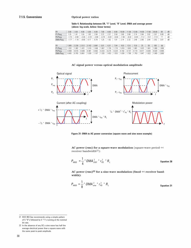
Optical power ratios
Table 4. Relationship between ER, "1" Level, "0" Level, OMA and average power (above: log scale, below: linear terms)
AC signal power versus optical modulation amplitude
AC power (rms) for a square-wave modulation (square-wave period << receiver bandwidth21):
Equation 30
AC power (rms)22 for a sine-wave modulation (fmod << receiver band-width):
Equation 31
30
7.1.5. Conversions
Current (after AC coupling)
t
Modulation power
t
P1 * rPD
OMA * rPD
Photocurrent
tP0
P1
Pavg OMA
Optical signal
tP1 * rPD
OMA * rPD * RL
1/4 * OMA2 * r2PD * RL
+ 1/2 * OMA * rPD
– 1/2 * OMA * rPD
Figure 31: OMA to AC power conversion (square wave and sine wave example)
LPDMOD RrOMAP ***41 22
0101=
LPDMOD RrOMAP ***81 22
sine=
ER 3.00 3.50 4.00 5.00 6.00 7.00 8.00 9.00 10.00 11.00 12.00 14.00 17.00 20.00 00 dBP1/Pavg 1.25 1.41 1.55 1.82 2.04 2.22 2.37 2.50 2.60 2.68 2.74 2.84 2.92 2.97 0.00 dBP0/Pavg –1.75 –2.09 –2.45 –3.18 –3.96 –4.78 –5.63 –6.50 –7.40 –8.32 –9.26 –11.2 –14.1 –17.0 ? ? dBOMA/Pavg –1.77 –1.16 –0.65 0.17 0.78 1.25 1.62 1.91 2.14 2.32 2.46 2.66 2.84 2.92 3.01 dB
ER 1.995 2.239 2.512 3.162 3.981 5.01 6.31 7.94 10.0 12.6 15.8 25 50 100 00P1/Pavg 1.332 1.382 1.431 1.519 1.598 1.667 1.726 1.776 1.818 1.853 1.881 1.923 1.961 1.980 1.000P0/Pavg 0.668 0.618 0.569 0.481 0.402 0.333 0.274 0.224 0.182 0.147 0.119 0.077 0.039 0.020 0.000OMA/Pavg 0.665 0.765 0.861 1.039 1.197 1.335 1.453 1.553 1.636 1.706 1.763 1.847 1.922 1.960 2.000
21 IEEE 802.3ae recommends using a simple pattern of 5 "0"s followed by 5 "1"s running at the nominal bit rate.22 In the absence of any DC a sine wave has half the average electrical power than a square wave with the same peak-to-peak amplitude.

31
Threshold when shot noise starts to exceed Thermal Noise (amplifier with Noise Figure NF23):
Equation 32
For T = 300K, F = 2.5 (8 dB), RL = 50 Ω , and rPD = 0.8 A/W, Equation 32 yields PTh = .8 mW (–1 dBm).
RIN Dynamic range when limited by thermal noise:
Equation 33
31
PDLTh rRe
FTkP***2
**=
( ) 2****
avgPDL PrRFTkRIN ≥
Name Symbol ValueAbsolute temperature (T0) 0 K (–237.15 °C)Boltzmann constant (k) 1.380651 * 10–23 J/K (= 8.617343 * 10–05 eV/K)Elementary charge (e) 1.602177 * 10–19 CPlank's constant (h) 4.135667 * 10–15 eVs (= 6.626069 * 10–34 Js)Speed of light (c) 2.997925 * 1008 m/s
7.2. Physical constants
21 Noise factor F = 10NF/10.

For more information on Agilent Technologies’ products, applications or services, please contact your local Agilent office. The complete list is available at:www.agilent.com/find/contactus
AmericasCanada (877) 894-4414Latin America 305 269 7500United States (800) 829-4444
Asia PacificAustralia 1 800 629 485China 800 810 0189Hong Kong 800 938 693India 1 800 112 929Japan 0120 (421) 345Korea 080 769 0800Malaysia 1 800 888 848Singapore 1 800 375 8100Taiwan 0800 047 866Thailand 1 800 226 008
Europe & Middle EastAustria 0820 87 44 11Belgium 32 (0) 2 404 93 40 Denmark 45 70 13 15 15Finland 358 (0) 10 855 2100France 0825 010 700* *0.125 €/minuteGermany 01805 24 6333** **0.14 €/minuteIreland 1890 924 204Israel 972-3-9288-504/544Italy 39 02 92 60 8484Netherlands 31 (0) 20 547 2111Spain 34 (91) 631 3300Sweden 0200-88 22 55Switzerland 0800 80 53 53United Kingdom 44 (0) 118 9276201Other European countries:www.agilent.com/find/contactusRevised: March 27, 2008
Product specifications and descriptions in this document subject to change without notice.
© Agilent Technologies, Inc. 2007, 2008Printed in USA, May 8, 20085989-5959ENwww.agilent.com/find/dca-j
Remove all doubtOur repair and calibration services will get your equipment back to you, performing like new, when promised. You will get full value out of your Agilent equipment throughout its lifetime. Your equipment will be serviced by Agilent-trained technicians using the latest factory calibration procedures, automated repair diagnostics and genuine parts. You will always have the utmost confidence in your measurements.
Agilent offers a wide range of additional expert test and measurement services for your equipment, including initial start-up assistance, onsite education and training, as well as design, system integration, and project management.
For more information on repair and calibration services, go to:
www.agilent.com/find/removealldoubt
www.agilent.com/find/openAgilent Open simplifies the process of connecting and programming test systems to help engineers design, validate and manufacture electronic products. Agilent offers open connectivity for a broad range of system-ready instruments, open industry software, PC-standard I/O and global support, which are combined to more easily integrate test system development.
www.agilent.com/find/emailupdatesGet the latest information on the products and applications you select.
www.agilent.com/find/agilentdirectQuickly choose and use your test equipment solutions with confidence.
Agilent Email Updates
Agilent Direct
AgilentOpen
www.agilent.com