diffraction inspired unidirectional and bidirectional · pdf filephotonic structures without...
TRANSCRIPT

Diffraction inspired unidirectional and bidirectional beam splitting in defect-containingphotonic structures without interface corrugationsEvrim Colak, Andriy E. Serebryannikov, P. V. Usik, and Ekmel Ozbay Citation: Journal of Applied Physics 119, 193108 (2016); doi: 10.1063/1.4949509 View online: http://dx.doi.org/10.1063/1.4949509 View Table of Contents: http://scitation.aip.org/content/aip/journal/jap/119/19?ver=pdfcov Published by the AIP Publishing Articles you may be interested in Controllable light diffraction in woodpile photonic crystals filled with liquid crystal Appl. Phys. Lett. 106, 021113 (2015); 10.1063/1.4905695 Experimental study of broadband unidirectional splitting in photonic crystal gratings with broken structuralsymmetry Appl. Phys. Lett. 102, 151105 (2013); 10.1063/1.4800147 50 ∕ 50 beam splitter using a one-dimensional metal photonic crystal with parabolalike dispersion Appl. Phys. Lett. 90, 251909 (2007); 10.1063/1.2750385 Line-defect-induced bending and splitting of self-collimated beams in two-dimensional photonic crystals Appl. Phys. Lett. 87, 181106 (2005); 10.1063/1.2112186 APL Photonics
Reuse of AIP Publishing content is subject to the terms at: https://publishing.aip.org/authors/rights-and-permissions. Download to IP: 139.179.98.142 On: Thu, 24 Nov 2016
11:46:41

Diffraction inspired unidirectional and bidirectional beam splittingin defect-containing photonic structures without interface corrugations
Evrim Colak,1 Andriy E. Serebryannikov,2,a) P. V. Usik,3 and Ekmel Ozbay4
1Electrical Engineering Department, Ankara University, Golbasi, 06830 Ankara, Turkey2Faculty of Physics, Adam Mickiewicz University, 61-614 Pozna�n, Poland3Institute of Radio Astronomy, National Academy of Sciences of Ukraine, 61002 Kharkiv, Ukraine4Nanotechnology Research Center—NANOTAM, Bilkent University, 06800 Ankara, Turkey
(Received 20 December 2015; accepted 2 May 2016; published online 20 May 2016)
It is shown that strong diffractions and related dual-beam splitting can be obtained at transmission
through the nonsymmetric structures that represent two slabs of photonic crystal (PhC) separated
by a single coupled-cavity type defect layer, while there are no grating-like corrugations at the
interfaces. The basic operation regimes include unidirectional and bidirectional splitting that occur
due to the dominant contribution of the first positive and first negative diffraction orders to the
transmission, which is typically connected with different manifestations of the asymmetric trans-
mission phenomenon. Being the main component of the resulting transmission mechanism, diffrac-
tions appear owing to the effect exerted by the defect layer that works like an embedded diffractive
element. Two mechanisms can co-exist in one structure, which differ, among others, in that
whether dispersion allows coupling of zero order to a wave propagating in the regular, i.e., defect-
free PhC segments or not. The possibility of strong diffractions and efficient splitting related to it
strongly depend on the dispersion properties of the Floquet-Bloch modes of the PhC. Existence of
one of the studied transmission scenarios is not affected by location of the defect layer. Publishedby AIP Publishing. [http://dx.doi.org/10.1063/1.4949509]
I. INTRODUCTION
Unidirectional transmission of electromagnetic waves1,2
and beam splitting3–5 belong to the functionalities, which are
widely used and highly demanded in practical devices work-
ing in different frequency ranges from microwaves to the visi-
ble. Recently, an approach has been suggested that enables
combination of these two functionalities in one Lorentz-
reciprocal device when two opposite incidence directions and
rather arbitrary directions of the outgoing beams (which differ
from the incidence direction) are allowed.6 Its realization with
the aid of a finite-thickness slab of two-dimensional photonic
crystal (PhC) with the rods made of isotropic, passive, linear
dielectric material, and one-side corrugations has been dem-
onstrated for the so-called direct regime of asymmetric trans-
mission.6,7 In this case, the ability of directional selectivity is
connected with the common effect of diffractions arising due
to the one-side interface corrugations and a specific, i.e., ani-
sotropic type or ultralow-index isotropic type dispersion of
the PhC, at which zero-order transmission is blocked, whereas
some of higher diffraction orders may be transmitted but only
at the corrugated-side incidence.7 On the other hand, strong
asymmetry in transmission and related asymmetry in beam
splitting can be obtained due to corrugations when dispersion
permits coupling of zero order at the noncorrugated incidence
interface (but it is suppressed in transmission), i.e., in the
inverse regime.8 In any case, placing corrugations at the inter-
faces has been the main route to obtain such diffractions that
are required for asymmetric transmission.
Asymmetric transmission is a very general phenomenon,
which can be connected not only with diffractions at the inter-
faces6–11 but also with polarization conversion,12–15 direction
manipulation by inclining interfaces like in prism-shaped con-
figurations,16–19 etc. Metamaterials may promise more com-
pact performances for devices based on diffraction inspired
asymmetric transmission,20–22 but their application to splitting
has not yet been studied. Moreover, it can be obtained in
transmission through thin corrugated structures with a slit23,24
and in-plane propagation of surface waves.25 The common
feature of all reciprocal devices based on asymmetric trans-
mission is that the spatial inversion symmetry is broken.
Clearly, they would not enable the same functionality as that
obtainable in the nonreciprocal framework, but at the same
time may enable such types of directional selectivity that are
useful for practical devices. In fact, asymmetric transmission
can be considered as the generalized mode conversion, which
is sensitive to the change of the incidence direction for the op-
posite one.26,27 One should also mention planar metamaterials
(metasurfaces) enabling beam manipulation, e.g., by using the
phase discontinuity approach.28–31
In this paper, we show that strong diffractions and split-
ting inspired by them can be obtained in nonsymmetric pho-
tonic structures without interface corrugations but with an
embedded diffractive element, which can be used as parts of
complex devices and circuits based on PhCs. The main goal
of this study is to demonstrate the principal possibility and
richness of both unidirectional and bidirectional splitting
regimes which are achievable for the studied class of the
structures in a wide range of parameter variation. We study
transmission in slabs of square-lattice rod-type dielectrica)Electronic mail: [email protected].
0021-8979/2016/119(19)/193108/9/$30.00 Published by AIP Publishing.119, 193108-1
JOURNAL OF APPLIED PHYSICS 119, 193108 (2016)
Reuse of AIP Publishing content is subject to the terms at: https://publishing.aip.org/authors/rights-and-permissions. Download to IP: 139.179.98.142 On: Thu, 24 Nov 2016
11:46:41

PhC with the embedded coupled-cavity type defect layer
that is composed of the same rods as the regular part of the
structure, which can be used to obtain splitting. The suitable
diffractions are created by the periodic defect layer that dis-
tinguishes the studied structures from those proposed earlier
for asymmetric transmission and unidirectional splitting. The
defect layer may, in principle, contribute to realization of
other functions (e.g., those directly connected with its defect
like nature like a defect-mode waveguide32,33) in other fre-
quency ranges in the same structure. This is especially prom-
ising from the multifunctional operation perspective. It will
be demonstrated that both direct and inverse regimes of
asymmetric transmission, with or without coupling of zero
order to a wave propagating in the regular part of PhC, can
yield efficient splitting. The possibility of obtaining of vari-
ous splitting regimes in the frequency ranges, which corre-
spond to different Floquet-Bloch modes of the PhC and,
thus, to different dispersion types, will be analyzed. The
main attention will be paid to the transmission results,
whereas dispersion results are used for the additional explan-
ations of the observed coupling scenarios. At the same time,
a figure-of-merit type quantifying of the splitting regimes
would be not practical, because a sole criterium is ambigu-
ous and requirements for the concrete device or circuit
should be taken into account that is beyond the scope of this
paper. To obtain transmission results, a flexible iterative
solver based on the coupled integral equation technique is
used; it has controllable convergence, which can be acceler-
ated by preconditioning.34 Dispersion is calculated using
CST Microwave Studio, a commercial solver based on finite
integration technique.35
II. GEOMETRY AND GENERAL PRINCIPLES
Figure 1 presents the general geometry of the studied
problem and schematics that illustrate the possible roles of
different parts of the entire nonsymmetric structure and
appropriate splitting scenarios. The studied nonsymmetric
structures represent a slab that consists of two segments of
two-dimensional square-lattice PhC with lattice constant a(denoted by A and C) and a coupled-cavity type defect layer
located between these two segments (denoted by B). It is
assumed that the segment A contains a smaller number of the
rod layers than the segment C. The structure is illuminated
by a normally incident s-polarized electromagnetic wave
(the electric field vector is along the rod axes) at the angle of
incidence h¼ 0, from either the upper or the lower side.
Consideration is restricted here to the case when defects in
the segment B are obtained by taking a single regular layer
of the rods (like those in the segments A and C), and then
removing every second rod so that the period along x-axis is
L¼ 2a. In fact, it determines the periodicity of the entire
structure, which is assumed to be infinite in the x-direction.
A difference in number of the layers within the segments
A and C is required in order to fulfill the requirement of bro-
ken spatial inversion symmetry, without which asymmetry in
transmission and, hence, unidirectional splitting cannot be
achieved.7,11 We consider a frequency range corresponding
to low-order Floquet-Bloch modes of PhC, to which higher
diffraction orders (jmj > 0) cannot be coupled when the
interface period is a.
Depending on whether the order m¼ 0 can be coupled
at the interfaces or not, two main groups of the transmission
scenarios can be distinguished. The difference is schemati-
cally demonstrated in Figs. 1(b) and 1(c). If zero order can be
coupled, the both segments A and C are in the propagating-
wave regime, while a properly designed layer B might create
redistribution of the wave energy in favor of higher orders,
which are also allowed to propagate in the regular segments
but cannot be coupled at h¼ 0 when the period is a. If zero
order cannot be in-coupled, we obtain evanescent-wave re-
gime in the segment A (at the upper-side illumination), while
the defect layer can transform evanescent waves into ones
allowed to propagate in the regular segments due to the higher
orders (jmj > 0). If the segment A contains just one or two
layers of the rods, evanescence might be weakly pronounced
so that the segments A and B should be considered rather
like a part of one complex grating, which does not have inter-
face corrugations. Note that Figs. 1(b) and 1(c) correspond
to the case when the segment A is adjusted to the incidence
interface. In case when the segment C is illuminated, the
segments A and C are formally in propagating-wave and
evanescent-wave regimes, respectively, for the scenario simi-
lar to Fig. 1(b), and both segments are in propagating-wave
regime for the scenario similar to Fig. 1(c).
FIG. 1. (a) General geometry of the finite-thickness slab of PhC with a
defect layer; schematics illustrating the roles of the defect layer at upper-
side illumination when zero order is either (b) not coupled or (c) coupled at
the upper interface, and (d) schematics showing the basic features of the
ideal diffraction inspired splitting at (left panel) upper-side illumination and
(right panel) lower-side illumination.
193108-2 Colak et al. J. Appl. Phys. 119, 193108 (2016)
Reuse of AIP Publishing content is subject to the terms at: https://publishing.aip.org/authors/rights-and-permissions. Download to IP: 139.179.98.142 On: Thu, 24 Nov 2016
11:46:41

Splitting can appear due to diffraction orders m¼61,
while zero order has to be suppressed in transmission, even
if it is efficiently in-coupled. Then, if transmission is fully
blocked at the opposite-side illumination, unidirectional
transmission takes place. In this case, zero order should not
be in-coupled, or in-coupled but insignificantly contributing
to the transmission due to a specific adjustment of structural
parameters. In the ideal case of unidirectional splitting, one
should obtain either
T! ¼ t!�1 þ t!þ1 and T ¼ 0 (1)
or
T ¼ t �1 þ t þ1 and T! ¼ 0; (2)
where T! and T mean total transmittance at the upper-side
and the lower-side illumination, respectively; t!61 and t 61
mean partial 61-order transmittance (diffraction efficiency)
at the upper-side and the lower-side illumination. The condi-
tions given by Eqs. (1) and (2) correspond to the direct re-
gime and the inverse regime of the diffraction inspired
unidirectional transmission, respectively. To avoid ambigu-
ity in the use of these regime names, we should note that
there is no full analogy with the structures having external
corrugations.8 However, it is expected that the main trans-
mission features can be similar so that the use of this termi-
nology is quite reasonable.
These two regimes correspond to the schematics shown
in the left and the right panel in Fig. 1(d). Earlier, it has been
shown for a slab of PhC with one-side corrugations that zero
order can be well (although not perfectly) suppressed, even
if being in-coupled.8 It is worth noting that the symmetry
properties result in that t!�1 ¼ t!þ1 and t �1 ¼ t þ1, according to
the general grating theory,36 whereas the reciprocity results
in that t0 ¼ t!0 ¼ t 0 . This means that dual-beam splitting
will appear if zero-order transmission is suppressed (t0¼ 0),
whereas the orders with jmj ¼ 1 may propagate due to the
segment B but those with jmj > 1 remain evanescent.6,8
In turn, splitting can be bidirectional, i.e., both T! and
T are quite high mainly due to the contribution of the
orders m¼61. However, it is difficult to obtain exactly
bidirectional dual-beam splitting with T! ¼ T and t!61
¼ t 61 in a nonsymmetric structure. Furthermore, suppression
of the propagating zero order can be problematic. Clearly,
enhancement or suppression of the corresponding counter-
parts of the resulting physical mechanism may yield a
more suitable configuration, e.g., in terms of efficiency.
Throughout the paper, we assume that the total number of
the rod layers in the segments A, B, and C is N¼ 12.
III. RESULTS AND DISCUSSION
A. Basic effects
Now, we analyze the results of numerical study that are
aimed to prove that the expected transmission and splitting
regimes can really appear in PhC based structures with an
embedded diffractive element. Figure 2 presents transmit-
tance vs kL (k¼x/c) for four nonsymmetric structures,
which differ from each other in location of the coupled-
cavity type defect layer. The value of e ¼ 5:8 is chosen here
that corresponds to the range to which some types of glass
and diamond do belong. In the kL-ranges where transmission
is forbidden at h¼ 0 for the corresponding uniform (i.e.,
defect-free) slab of PhC, the field can still be strong at the
second layer location. Thus, in contrast with evanescence
expected to appear when the segment A contains several reg-
ular layers of the rods, the most upper regular layer can be
considered in this case just as a part of the complex grating
with internal corrugations. Then, coupling to propagating
waves due to higher diffraction orders and the resulting
transmission might be quite strong. Indeed, one can see in
Fig. 2(a) two such kL-ranges with T! � t!�1 þ t!þ1, which are
denoted by 1 and 3. They are located at 8:1 < kL < 9:4 and
10:6 < kL < 11:0, respectively. Since t!�1 ¼ t!þ1, these
ranges are suitable for dual-beam splitting, although optimi-
zation is needed to obtain higher efficiency.
Two more ranges of interest are denoted by 2 and 4.
They are located at 9:4 < kL < 10:6 and kL> 11.0, where
zero order contributes to T!. In the range 2, we obtain
t!�1 ¼ 0, and hence, T! ¼ t0. In the range 4, t!�1 > 0, and
thus, T! ¼ t0 þ t!�1 þ t!þ1 in the general case. In a larger part
of this range, diffractions are strong, i.e., t!�1 þ t!þ1 � t0. As
a result, dual-beam splitting can be obtained that is imperfect
because of the contribution of t0. In fact, a sole irregular in-
ternal layer may fully change the transmission scenario as
compared to the uniform slab of PhC with the same N, for
which either perfect reflection (ranges 1 and 3) or zero-order
transmission (ranges 2 and 4) could only be possible at h¼ 0
(not shown).
Next, let us shift the defect layer downward so that it
becomes the third and, then, the fourth layer from the upper
FIG. 2. Transmittance vs kL for structure with defect layer being (a) second,
(b) third, (c) fourth, and (d) fifth one from the upper (here incidence) inter-
face; d=a ¼ 0:4; e ¼ 5:8; solid blue line t0, dashed red line t!�1 and t!þ1, dot-
ted cyan line T!.
193108-3 Colak et al. J. Appl. Phys. 119, 193108 (2016)
Reuse of AIP Publishing content is subject to the terms at: https://publishing.aip.org/authors/rights-and-permissions. Download to IP: 139.179.98.142 On: Thu, 24 Nov 2016
11:46:41
interface, see Figs. 2(b) and 2(c). This means that the number
of the rod layers of the segment A being in the evanescent-
wave regime is increased, leading to the decrease of T!
within the kL-ranges denoted by 1 and 3. However, the
extent of decrease for these ranges is different, being con-
nected with different properties of Floquet-Bloch modes and,
thus, with different coupling conditions. For the range 4, one
should notice a weak effect of zero order, strong diffractions,
and the related potential in splitting. These features remain
whatever the depth of the defect layer embedding is. This
gives big freedom in design, i.e., the defect layer may be
involved in realization of another functionality (not consid-
ered here), which requires a deep embedding of this layer.32,33
In Fig. 2(d), transmittance is shown for the structure, in
which the defect layer is the fifth one from the upper interface,
while the segment C contains seven regular layers. For such a
structure, evanescent waves may be strongly damped when
zero order is not coupled at the upper incidence interface.
Now, T! � 0 in the range 1. In the range 3, in-coupling to
the evanescent waves and their transformation into the propa-
gating waves at the segment B results in non-vanishing trans-
mission. For instance, T! � t!�1 þ t!þ1 exceeds 0.12 and 0.09
at 10:6 < kL < 11 in Figs. 2(c) and 2(d), respectively.
One more interesting feature is observed at the right
edge of the range 2 in Figs. 2(c) and 2(d), where significant
contribution of the orders m¼61 to T! occurs near
kL¼ 10.45, at which t�1 � 0 and tþ1 � 0 in Fig. 2(a). Thus,
contribution of the orders m ¼ 61 can strongly depend on
the thicknesses of the segments A and C.
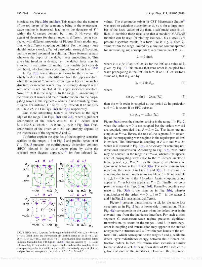
To further explain the specifics of the coupling scenarios
realized in the ranges 1–4 in Fig. 2 and predict behavior of
T , Fig. 3 presents the equifrequency dispersion contours
(EFCs) plotted in the wave vector plane by using the
repeated zone diagram approach,7,37 for four selected kL-
values. The eigenmode solver of CST Microwave Studio35
was used to calculate dispersion as kx vs x for a large num-
ber of the fixed values of ky; then, a self-made code is uti-
lized to combine these results so that a standard MATLAB
function can be used for plotting isolines. This allows us to
present dispersion results in a form like in Fig. 3. Each kx-
value within the range limited by a circular contour (plotted
for surrounding air) corresponds to a certain value of h, i.e.,
kx ¼ k sin h; (3)
where k ¼ x=c. If an EFC exists for the PhC at a value of kx
given by Eq. (3), this means that zero order is coupled to a
wave propagating in the PhC. In turn, if an EFC exists for a
value of kx that is given by
kx ¼ k sin /m; (4)
where
sin /m ¼ sin hþ 2pm=ðkLÞ; (5)
then the m-th order is coupled at the period L. In particular,
at h¼ 0, it occurs if an EFC exists at
sin /61 ¼ 62p=ðkLÞ: (6)
Figure 3(a) shows the situation arising in the range 1 in Fig. 2,
when the order m¼ 0 is not coupled but the orders m¼61
are coupled, provided that P ¼ L ¼ 2a. The latter are not
coupled at P¼ a. Hence, the role of the segment B in obtain-
ing of the propagating-wave regime in the regular part of PhC
is evident. The difference in coupling at P¼ a and P ¼ 2a,
which is illustrated in Fig. 3(a), is necessary for obtaining uni-
directional transmission. According to Fig. 3(b), zero order
may be coupled in the range 2 at P¼ a, whereas the appear-
ance of propagating waves due to the 61-orders invokes a
larger period, e.g., P ¼ 2a. For the range 2, we obtain good
agreement between Figs. 2 and 3(b). The same remains true
regarding the range 3 in Figs. 2 and 3(c). In this case, in-
coupling due to zero order is impossible at h¼ 0 but possible
at jkxj=k � 0:6 due to the 61-orders. Again, coupling cannot
appear at P¼ a but can appear at P ¼ 2a. Finally, we com-
pare the range 4 in Figs. 2 and 3(d). Formally, coupling sce-
nario in Fig. 3(d) is the same as in Fig. 3(b), whereas
contribution of the orders m¼ 0, 61 to T! in the ranges 2
and 4 in Fig. 2 is substantially different.
Figure 4 presents transmittance vs kL for the same four
structures as in Fig. 2 but at lower-side illumination. Thus,
Fig. 4(a) corresponds to the case when the defect layer is the
eleventh one from the incidence interface. For such a thick
segment C, evanescent-wave regime prevents significant
transmission, as occurs in the ranges 1 and 3. In turn, zero-
order in-coupling and transmission may appear in the studied
nonsymmetric structure at h¼ 0 within pass bands of the uni-
form PhC, which correspond to the ranges 2 and 4, while the
defect layer redistributes energy between the different dif-
fraction orders. In fact, this transmission scenario is similar
to that studied in Ref. 8 for uniform slabs of PhC with corru-
gations at one of the interfaces. However, the difference
FIG. 3. EFCs in (kx, ky)-plane for the regular infinite PhC with d=a ¼ 0:4 and
e ¼ 5:8 (solid lines) and surrounding air (dashed lines) at (a) kL¼ 8.7, (b)
kL¼ 10, (c) kL¼ 10.7, and (d) kL¼ 11.7. Construction lines (vertical dotted
lines) are located in line with Eqs. (4) and (5); they are denoted by �1, 0, and
þ1 according to their order (m). Signs þ and � indicate that coupling of the
corresponding order is possible or impossible, respectively; signs at plot top
and plot bottom correspond to the periods of P ¼ L ¼ 2a and P¼ a.
193108-4 Colak et al. J. Appl. Phys. 119, 193108 (2016)
Reuse of AIP Publishing content is subject to the terms at: https://publishing.aip.org/authors/rights-and-permissions. Download to IP: 139.179.98.142 On: Thu, 24 Nov 2016
11:46:41

from Ref. 8 is that now we have two segments, A and C, in
propagating-wave regime.
Let us compare the ranges 1 and 3 in Figs. 2 and 4 from
the point of view of asymmetry in transmission. In Figs. 2(a)
and 4(a), one can see that T! ¼ t!�1 þ t!þ1 > 0 and T � 0.
Shifting the defect layer one period lower [see Figs. 2(b) and
4(b)], two periods lower [see Figs. 2(c) and 4(c)], and,
finally, four periods lower [see Figs. 2(d) and 4(d)] does not
affect the strong damping that remains in the ranges 1 and 3
in Figs. 4(a)–4(d). However, well-pronounced asymmetry in
transmission and related unidirectional dual-beam splitting
can be obtained in these ranges in the direct regime (T! > 0
and T ¼ 0) only when the defect layer is rather close to the
upper interface.
Next, we consider the ranges 2 and 4 in Figs. 2 and 4.
Although contribution of t0 to T! and T is possible, the role
of higher orders can be dominant and, thus, diffraction
inspired dual-beam splitting can still be realized. In these
ranges, in-coupling can be obtained due to zero order, with
redistribution of the wave energy in favor of the 61-orders
occurring at the segment B. In the range 2, the effect of loca-
tion of the defect layer on the achievable values of T is sig-
nificant. Since t!�1 � 0 [except for vicinity of kL¼ 10.5 in
Figs. 2(c) and 2(d)], we obtain well pronounced asymmetry in
transmission and unidirectional splitting in the inverse regime,
when the defect layer is close to the exit interface. For
instance, T ¼0:92; t0�0:17 at kL¼9.54 and T ¼0:88;t0�0:05 at kL¼9.66, both in Fig. 4(a), and T ¼0:8; t0
¼1:4�10�2 at kL¼9.58 in Fig. 4(b). Multiple Fabry-Perot
type peaks of T with the main contribution of the61-orders,
which are observed in Fig. 4, indicate similarities of the
resulting mechanism to that studied in Ref. 8.
In the range 4, better suppression of zero order and split-
ting can be achieved for different locations of the defect
layer. In the general case, splitting occurs for the both inci-
dence directions, whereas T! 6¼ T ðT! > 0; T > 0Þ,except for some peculiar values of kL. In Fig. 4, it is seen
that strong transmission (e.g., T > 0:9) can be obtained in
the range 4 at the lower-side illumination, even if t0� 0.
This occurs, for example, at kL¼ 11.95 in Fig. 4(b) and at
kL¼ 11.2 in Fig. 4(c). Two maxima of the nearly perfect
transmission are noticeable: T > 0:99; t0 � 0:45 at kL¼ 10.4 in Fig. 4(a) and T > 0:95; t0 � 0:48 at kL¼ 10.37
in Fig. 4(b). However, contribution of t0 is not vanishing in
these cases. Note that the number and location of the maxima
of t �1 and T in the ranges 2 and 4 can also depend on loca-
tion of the defect layer, see Fig. 4. The possible reason is
that a thicker PhC segment (segment C) can create Fabry-
Perot type maxima located denser than those created by a
thinner one (segment A). In the other cases, transmission can
be stronger at the upper-side illumination, e.g., T! ¼ 0:69 at
kL¼ 11.36 in Fig. 2(a), T! ¼ 0:82 at kL¼ 11.45 in Fig. 2(c)
whereas T � 0, and T! ¼ 0:88 at kL¼ 11.32 in Fig. 2(d)
whereas T ¼ t0 � 0:03.
To further demonstrate asymmetry in transmission,
Fig. 5 presents the contrast r ¼ 20 log10ðT!=T Þ and t!�1 to-
gether with t �1 for the range 4. In Fig. 5(a), it is seen that the
contrast, a quantity connected with unidirectionality of split-
ting, is high in the ranges 1 and 3, also at a rather deep
embedding of the defect layer. However, a suitable value of
r can correspond to maxðT!; T Þ being not large enough.
This situation is typical for the direct regime in the range 1.
In the inverse regime in the range 2, one can obtain jrj> 20 dB, at least if the defect layer is not deeply embedded.
A proper combination of transmission efficiency and contrast
can be obtained in the range 3. However, its practical use for
unidirectional splitting is again restricted to the cases when
the embedding is not deep. The specifics and potential of the
range 4 in splitting are determined by the fact that strong
diffractions can appear at the both incidence directions.
Figure 5(b) illustrates that the real bidirectional splitting, i.e.,
with g ¼ t!�1 ¼ t!þ1 ¼ t �1 ¼ t!þ1 (g¼ 0.4 at kL¼ 11.62) and
unidirectional splitting in the inverse regime with t �1 � t!�1
(near kL¼ 11.95, jrj ¼ 116) can be obtained in one structure
and, furthermore, at the close frequencies which correspond
FIG. 4. Transmittance vs kL for structure with defect layer being (a) second, (b)
third, (c) fourth, and (d) fifth one from the upper (here exit) interface; d=a¼0:4; e¼5:8; solid blue line t0, dashed red line t �1 and t þ1, dotted cyan line T .
FIG. 5. (a) Contrast r ¼ 20 log10ðT!=T Þ for the structures in Figs. 2 and 4
when defect layer is second (solid line), third (dashed line), fourth (dotted
line), and fifth (dash-dotted line) layer from the upper interface; (b) t!�1
dashed red line and t �1 solid gray line, for the structures with defect layer
being the third one from the upper interface, as in Figs. 2(b) and 4(b); rectan-
gle and asterisk indicate the cases with t!�1 ¼ t �1 and t �1=t!�1 � 10,
respectively.
193108-5 Colak et al. J. Appl. Phys. 119, 193108 (2016)
Reuse of AIP Publishing content is subject to the terms at: https://publishing.aip.org/authors/rights-and-permissions. Download to IP: 139.179.98.142 On: Thu, 24 Nov 2016
11:46:41

to the same Floquet-Bloch mode. Note that bidirectional
splitting with 0.3< g< 0.4 is also observed in Figs. 2(c),
2(d), 4(c), and 4(d), i.e., at different locations of the defect
layer. The same remains true regarding the inverse regime of
unidirectional splitting. However, the real bidirectionality
case illustrated in Fig. 5(b) at kL¼ 11.62 seems more useful
for practical purposes. Since t!61 ¼ t 61, a symmetric grating
is mimicked and lack of symmetry is masked in this case.
B. Varying structural parameters
In line with the goals of this study, we demonstrate now
generality of the effects observed in Figs. 2–5. Adjusting the
material and geometrical parameters, one can obtain a nearly
perfect unidirectional transmission, while zero order does
not contribute to transmission. An example is presented in
Fig. 6, where transmittance is shown at both lower-side and
upper-side illumination for the structure which differs from
that in Figs. 2 and 4 just in the rod material. The value of e ¼11:4 is chosen here, which corresponds to the e-range, to
which Si, GaAs, and other widely used materials do belong.
Comparing to the ranges 1 and 3 in Figs. 2 and 4, we obtain
now higher efficiency, i.e., T! ¼ t!�1 þ t!þ1 > 0:95 at kL¼ 7,
whereas T � 0 in a wide kL-range. Note that coupling to
all of the propagating orders, i.e., m¼ 0, 61 is formally
allowed at kL> 7.05 by the EFCs (not shown). The peak of
T! ¼ t0 þ t!�1 þ t!þ1 > 0:99 at kL¼ 7.16 [the highest peak in
Fig. 6(a)] should also be noticed. However, it does not allow
obtaining a nearly perfect splitting, since t0 � 0:15.
Next, we consider a structure with thinner rods that are
made of material with e¼ 9.61 (Al2O3 below 2 THz), at
upper-side illumination and the corresponding case of lower-
side illumination, see Figs. 7 and 8, respectively. There are
three typical kL-ranges denoted by 2, 3, and 4, which are
similar to the ranges denoted by the same numbers in Figs.
2–6. Indeed, zero order can be coupled to a Floquet-Bloch
wave of the PhC in the ranges 2 and 4, whereas only the 61-
orders can be coupled in the range 3 due to the defect layer
with period P ¼ L ¼ 2a. Alongside the similarity of the
ranges 3 and 4 to the corresponding ranges in Figs. 2–6, un-
usual behavior of transmission in the range 2 should be
noticed. Therein, zero order can be well suppressed in
transmission, in spite of being in-coupled. In this range,
T! � 0 in Fig. 7(a), while T > 0:5 at the maxima due to
the 61-orders in Fig. 8(a).
The effect of location of the defect layer strongly differs
from one range to another. It is expected to depend on the
properties of the corresponding Floquet-Bloch wave(s) and
in-coupling conditions. For instance, if zero order may be
in-coupled, location of the defect layer does not affect the
principal possibility of splitting, except for the range 2 in
FIG. 6. Transmittance vs kL for structure with defect layer being the second
layer from the upper interface at (a) upper-side and (b) lower-side incidence;
d=a ¼ 0:4; e ¼ 11:4; solid blue line t0, dashed red line (a) t!�1 ¼ t!þ1 and (b)
t �1 ¼ t þ1, dotted cyan line (a) T! and (b) T .
FIG. 7. Transmittance vs kL for structure with defect layer being (a) second,
(b) third, (c) fourth, and (d) fifth one from the upper (here incidence) inter-
face; d=a ¼ 0:3; e ¼ 9:61; solid blue line t0, dashed red line t!�1 and t!þ1, dot-
ted cyan line T!.
FIG. 8. Transmittance vs kL for structure with defect layer being (a) second,
(b) third, (c) fourth, and (d) fifth from the upper (here exit) interface;
d=a ¼ 0:3; e ¼ 9:61; solid blue line t0, dashed red line t �1 and t þ1, dotted
cyan line T .
193108-6 Colak et al. J. Appl. Phys. 119, 193108 (2016)
Reuse of AIP Publishing content is subject to the terms at: https://publishing.aip.org/authors/rights-and-permissions. Download to IP: 139.179.98.142 On: Thu, 24 Nov 2016
11:46:41

Fig. 7(a), where transmission is suppressed. On the contrary,
if zero order may not be coupled, but the incidence interface
cannot itself create the 61-orders, efficient tunneling
through the segment A would be necessary. In this case, the
defect layer should transform evanescent waves into the
higher-order waves propagating in the segment C. However,
as seen in Fig. 7(d), four regular layers located between the
incidence interface and the defect layer can be sufficient to
suppress evanescent waves so that T! � 0 in the range 3. At
lower-side illumination, transmittance in the ranges 2, 3, and
4 in Fig. 8 behaves similar to the ranges denoted with the
same numbers in Fig. 4. The only significant difference
is probably that t0 is suppressed in the entire range 2 in
Figs. 7(a) and 8(a) and, since t!0 ¼ t 0 , splitting with T
¼ t �1 þ t þ1 can be obtained while T! � 0. At some maxima
of T , the defect layer works like a nearly perfect order
convertor.
Figure 9 presents t!�1 and t �1 at 9:4 < kL < 10 for two
structures from Figs. 7 and 8. In Fig. 9(a), there are three
maxima of t �1 > 0:45, at which t!�1 < 0:01 (denoted by
asterisks). For one of them, t �1 � 0:49 (near kL¼ 9.82), that
is closest to the ideal unidirectional splitting. Changing loca-
tion of the defect layer, one can obtain different combina-
tions of splitting regimes in one structure. For example, in
Fig. 9(b) one can see that splitting with the features typical
for asymmetric transmission in the inverse and the direct re-
gime can appear at close frequencies, although transmission
efficiency and contrast remain a subject of optimization.
In particular, t �1 ¼ 0:45 and t!�1 ¼ 0:05 near kL¼ 9.75, t!�1
¼ 0:32 and t �1 ¼ 3:6� 10�2 near kL¼ 9.78, and t �1 ¼ 0:43
and t!�1 ¼ 7� 10�3 near kL¼ 9.86 (denoted by asterisks).
Such regimes can be important for obtaining of multifunc-
tional operation that might include regimes with the waves
guided by the defect layer,33 for which this layer should
be located quite far from the incidence interface, like in
Fig. 9(b). Note that a similar combination of unidirectional
splitting regimes that would utilize one of the Floquet-Bloch
modes as in the case considered has not yet been found in
the nonsymmetric structures with one-side corrugations,
e.g., see Ref. 8. It is noteworthy that combination of the
direct and inverse regimes of unidirectional splitting can also
be obtained in one structure in Figs. 7(b) and 8(b), and in
Figs. 7(c) and 8(c). Besides, the real bidirectional splitting
like that discussed in Fig. 5(b) can be obtained in the range 4
for the structures in Figs. 7(a)–7(d) and 8(a)–8(d). However,
the case in Fig. 5(b) can be more appropriate because of
higher efficiency and a peculiar combination of splitting
regimes.
An example demonstrating that even a weak variation in
d/a may lead to strong differences in transmission is pre-
sented in Fig. 10, where a bit larger value of d/a than in Figs.
7–9 is used. The ranges are numbered in the same manner as
in Figs. 2–8. In particular, one should notice a higher effi-
ciency within the range 3, where T! ¼ t!�1 þ t!þ1 and
T � 0. For instance, T! ¼ 0:92 at kL¼ 10.05 and T! ¼0:89 at kL¼ 10.25 in Fig. 10(a). Hence, performance of uni-
directional direct-regime splitters can be enhanced by simple
parameter adjustment. Moreover, the possibility of unidirec-
tional inverse-regime splitting in the range 2 remains. For
example, T ¼ t �1 þ t þ1 ¼ 0:95 and T! � 1:1� 10�2 near
kL¼ 9.35 in Figs. 10(a) and 10(b). Comparing Fig. 10(a)
with Fig. 10(b) and Fig. 10(c) with Fig. 10(d), one can see
that the shift of the defect layer one period lower is still
appropriate for the use of the range 3 for unidirectional split-
ting. On the contrary, the range 1 is not useful at all because
of low efficiency, even if the defect layer is the second upper
one, as in Fig. 10(a). The transmission features in the range 2
are rather similar to those in the same range in Figs. 2 and 4.
It is worth noting that now the range 4 is less useful, since
zero order contributes stronger than in the previous exam-
ples. The above discussed possibility of efficient suppression
of zero order without utilizing the blocking effect connected
with the specific EFC features and possibility of combining
direct and inverse regimes in such a manner like in Fig. 9(b)
enables more flexibility, on the one hand, but imposes
restrictions on fabrication accuracy, on the other hand.
Finally, we demonstrate a way to wideband unidirec-
tional splitting, at which transmission remains strong
between the neighboring maxima. In fact, it exploits the
merging of the maxima with the dominant contribution of
higher orders. It can be achieved in the structures that are
FIG. 9. t!�1 (dashed red line) and t �1 (solid gray line) for (a) structure from
Figs. 7(a) and 8(a) and (b) structure from Figs. 7(d) and 8(d); asterisks indi-
cate selected cases with maxðt �1=t!; t!�1=t �1Þ > 8.
FIG. 10. Transmittance vs kL for structure with defect layer being (a) second
and (b) third layer from the upper incidence interface, and (c) second and (d)
third layer from the upper exit interface; d=a ¼ 0:32; e ¼ 9:61; solid blue
line t0; dashed red line (a) and (b) t!�1 and t!þ1, and (c) and (d) t �1 and t þ1;
dotted cyan line (a) and (b) T! and (c) and (d) T .
193108-7 Colak et al. J. Appl. Phys. 119, 193108 (2016)
Reuse of AIP Publishing content is subject to the terms at: https://publishing.aip.org/authors/rights-and-permissions. Download to IP: 139.179.98.142 On: Thu, 24 Nov 2016
11:46:41

similar to those in Figs. 2, 4, 7, and 8 but modified by remov-
ing one layer of the rods from the segment C. Figure 11
presents transmittance in the case when the layer that is the
sixth one from the upper interface is removed so that there
are more six regular layers of the rods below the new line
defect. In Fig. 11(a), a desired band with T! ¼ t!�1 þ t!þ1 >0:65 and T � 0 is located around kL¼ 11.2. Two wide
bands with t �1 þ t þ1 exceeding 0.78 and 0.62 are obtained in
the inverse regime in Fig. 11(b) near kL¼ 9.6 and kL¼ 10,
respectively. However, maxt0 is equal to 0.06 and 0.15 for
these bands, i.e., unidirectionality is imperfect. (Note that in
Fig. 11(b) we obtain T > 0:99 at kL¼ 9.99). Hence, one
should find a compromise between the extent to which uni-
directionality is pronounced and number of the bands suita-
ble for wideband splitting. Wideband unidirectional splitting
can be obtained in the direct regime also for the second
performance, see Fig. 11(c). In this case, only the lower-
frequency part of the band located around kL¼ 10.6 is uni-
directional, i.e., t0 � 0 and T � 0, although all of the
orders m¼ 0 and m¼61 may formally contribute to T!.
Wideband splitting observed in the inverse regime in
Fig. 11(d) at kL¼ 9.53 seems to be a compromise between
efficiency and strength of unidirectionality in terms of
maxðT =t0Þ and maxðT =T!Þ. To further characterize
asymmetry in transmission at wideband splitting in Fig. 11,
Fig. 12 presents t!�1 and t �1 at upper-side and lower-side illu-
mination in one plot, for each of the two performances from
Fig. 11. Possibility of better suppression of zero order, which
is allowed to be coupled, and main features of the band wid-
ening mechanism that is based on twinning and merging of
the transmission maxima invoke a more detailed study.
IV. CONCLUSION
To summarize, we studied the potential of photonic
crystal (PhC) based structures, whose spatial inversion sym-
metry is broken by using a periodic defect layer, in diffrac-
tion inspired dual-beam splitting. We demonstrated what and
how can be achieved and what might be difficult to achieve
for this class of the structures. The basic splitting mecha-
nisms that have earlier been studied in the nonsymmetric
PhC based structures with interface corrugations are obtained
in this paper for similar photonic structures that do not have
external corrugations. Various regimes of unidirectional and
bidirectional splitting have been discussed. It is shown that
zero order can be well suppressed even if its coupling to a
Floquet-Bloch mode of the PhC is allowed by the dispersion.
Moreover, it can be the only order that contributes to in-
coupling, whereas higher orders required for a propagating-
wave regime are created by the energy redistribution at the
embedded defect layer. Thus, unidirectional splitting, whose
existence has often been associated with blocking of zero-
order transmission owing to the specific dispersion proper-
ties, is a general regime obtainable at different combinations
of dispersion, material, and geometrical characteristics.
Furthermore, strong higher-order transmission and related
splitting can appear for two opposite incidence directions in
the neighboring frequency ranges, depending on dispersion
and coupling conditions. As follows from the obtained
results, the defect layer should be located not far from one of
the interfaces in order to obtain unidirectional splitting in the
direct regime. In the inverse regime, it can be achieved also
for a deeply embedded defect layer. This feature and high
capability of integration with other devices on the PhC plat-
form are very important for future applications of the struc-
tures with the embedded defects in multifunctional and
reconfigurable devices, in which the same defect layer may
work, for instance, like a waveguide in another frequency
range in the same structure.
Compared to the earlier studies of the nonsymmetric
structures with one-side external corrugations, some peculiar
regimes may show even better characteristics. Clearly, this
does not mean that the structures with external corrugations
may not show better characteristics in principle but rather
indicates that not all of them have already been found. In
particular, this is related to the inverse-regime dual-beam
unidirectional splitting and reversing direction of high-
efficiency transmission at unidirectional splitting for weak
frequency variations. It is noteworthy that bidirectional split-
ting can be achieved at the deep embedding of the defect
layer. In particular, the real bidirectional splitting should be
FIG. 11. Transmittance vs kL for two structures with coupled-cavity type
defect layer being (a) and (c) second layer from the upper incidence inter-
face and (b) and (d) second layer from the upper exit interface, and addi-
tional line defect that is sixth layer from (a) and (c) the upper incidence
interface and (b) and (d) the upper exit interface; (a) and (b) d=a ¼ 0:4; e ¼5:8 and (c) and (d) d=a ¼ 0:32; e ¼ 9:61; solid blue line t0, dashed red line
(a) and (c) t!�1 ¼ t!þ1 and (b) and (d) t �1 ¼ t þ1, dotted cyan line (a) and (c)
T! and (b) and (d) T .
FIG. 12. t!�1 (red dashed line) and t �1 (navy solid line) for the structures
from (a) Figs. 11(a) and 11(b), and (b) Figs. 11(c) and 11(d); circles and
crosses indicate the cases of wideband splitting that is connected with
inverse and direct unidirectional transmission regimes, respectively.
193108-8 Colak et al. J. Appl. Phys. 119, 193108 (2016)
Reuse of AIP Publishing content is subject to the terms at: https://publishing.aip.org/authors/rights-and-permissions. Download to IP: 139.179.98.142 On: Thu, 24 Nov 2016
11:46:41

mentioned, at which transmission and diffraction at some
frequencies are exactly the same for two opposite incidence
directions, in spite of that the structure is nonsymmetric with
respect to the midplane (y¼D/2, D is the thickness of the
entire slab). In the other words, the lack of symmetry is not
recognizable in the transmittance data. The obtained results
indicate a route to future multifunctional devices and related
directions of perspective research. Since the dielectric mate-
rials, which are suggested for the use, are low-loss and
weakly dispersive in a wide frequency range including
microwave and optical frequencies, the studied structures
should be rescalable within this range. Possible realization of
the suggested approach with the aid of metamaterials will be
a subject of one of the next studies.
ACKNOWLEDGMENTS
This work is supported by the Projects DPT-HAMIT,
ESF-EPIGRAT, and NATO-SET-181, and by TUBITAK
under the Project Nos. 107A004, 109A015, and 109E301.
A.E.S. thanks TUBITAK for partial support in the
framework of the Visiting Researcher Program and National
Science Centre, Poland for financial assistance under the
Projects MagnoWa DEC-2-12/07/E/ST3/00538, and MetaSel
DEC-2015/17/B/ST3/00118. E.O. acknowledges partial
support from the Turkish Academy of Sciences.
1A. Figotin and I. Vitebskiy, Phys. Rev. B 67, 165210 (2003).2F. D. M. Haldane and S. Raghu, Phys. Rev. Lett. 100, 013904 (2008).3M. Schmitz, R. Br€auer, and O. Bryngdahl, Opt. Lett. 20, 1830 (1995).4Ph. Lalanne, J. Hazart, P. Chavel, E. Cambril, and H. Launois, J. Opt. A:
Pure Appl. Opt. 1, 215 (1999).5J. Feng and Z. Zhou, Opt. Lett. 32, 1662 (2007).6E. Colak, A. E. Serebryannikov, A. O. Cakmak, and E. Ozbay, Appl. Phys.
Lett. 102, 151105 (2013).7A. E. Serebryannikov, Phys. Rev. B 80, 155117 (2009).8A. E. Serebryannikov, K. B. Alici, T. Magath, E. Colak, and E. Ozbay,
Phys. Rev. A 86, 053835 (2012).9S. Xu, C. Qiu, and Z. Liu, J. Appl. Phys. 111, 094505 (2012).
10A. Mandatori, M. Bertolotti, and C. Sibilia, J. Opt. Soc. Am. B 24, 685 (2007).
11X.-F. Li, X. Ni, L. Feng, M.-H. Lu, C. He, and Y.-F. Chen, Phys. Rev.
Lett. 106, 084301 (2011).12R. Singh, E. Plum, C. Menzel, C. Rockstuhl, A. K. Azad, R. A. Cheville,
F. Lederer, W. Zhang, and N. I. Zheludev, Phys. Rev. B 80, 153104
(2009).13J. H. Shi, H. F. Ma, C. Y. Guan, Z. P. Wang, and T. J. Cui, Phys. Rev. B
89, 165128 (2014).14Y. Xu, Q. Shi, Z. Zhu, and J. Shi, Opt. Express 22, 25679 (2014).15M. Mutlu, S. Cakmakyapan, A. E. Serebryannikov, and E. Ozbay, Phys.
Rev. B 87, 205123 (2013).16C. Wang, X.-L. Zhong, and Z.-Y. Li, Sci. Rep. 2, 674 (2012).17A. Cicek, O. A. Kaya, and B. Ulug, Appl. Phys. Lett. 100, 111905
(2012).18F. T. Gundogdu, A. E. Serebryannikov, A. O. Cakmak, and E. Ozbay, Opt.
Express 23, 24120 (2015).19J. H. Oh, H. W. Kim, P. S. Ma, H. M. Seung, and Y. Y. Kim, Appl. Phys.
Lett. 100, 213503 (2012).20M. Beruete, A. E. Serebryannikov, V. Torres, M. Navarro-Cia, and M.
Sorolla, Appl. Phys. Lett. 99, 154101 (2011).21T. Xu and H. J. Lezec, Nat. Commun. 5, 4141 (2014).22P. Rodriguez-Ulibarri, V. Pacheco-Pena, M. Navarro-Cia, A. E.
Serebryannikov, and M. Beruete, Appl. Phys. Lett. 106, 061109 (2015).23M. Stolarek, M. Yavorskiy, R. Kotynski, C. J. Zapata Rodriguez, J.
Lusakowski, and T. Szoplik, Opt. Lett. 38, 839 (2013).24S. Cakmakyapan, A. E. Serebryannikov, H. Caglayan, and E. Ozbay, Opt.
Express 20, 26636 (2012).25V. Kuzmiak and A. A. Maradudin, Phys. Rev. A 86, 043805 (2012).26F. V. Liu, D. A. B. Miller, and S. Fan, Opt. Express 20, 28388 (2012).27L. Feng, M. Ayache, J. Huang, Y.-L. Xu, M.-H. Lu, Y. F. Chen, Y.
Fainman, and A. Scherer, Science 333, 729 (2011).28N. Yu, P. Genevet, M. Kats, F. Aieta, J.-P. Tetienne, F. Capasso, and Z.
Gaburro, Science 334(6054), 333 (2011).29F. Aieta, P. Genevet, N. Yu, M. Kats, Z. Gaburro, and F. Capasso, Nano
Lett. 12, 1702 (2012).30C. Pfeiffer and A. Grbic, Phys. Rev. Lett. 110, 197401 (2013).31A. Mehdipour, J. W. Wong, and G. V. Eleftheriades, IEEE Trans.
Antennas. Propag. 63, 978 (2015).32K. Sakoda, Optical Properties of Photonic Crystals (Springer, Berlin,
2001).33Photonic Crystals. Physics, Fabrication and Applications, edited by K.
Inoue and K. Othaka (Springer, Berlin, 2004).34T. Magath and A. E. Serebryannikov, J. Opt. Soc. Am. A 22, 2405
(2005).35See www.cst.com for software details.36R. Petit, Electromagnetic Theory of Gratings (Springer, Berlin, 1980).37S. Foteinopoulou and C. M. Soukoulis, Phys. Rev. B 72, 165112 (2005).
193108-9 Colak et al. J. Appl. Phys. 119, 193108 (2016)
Reuse of AIP Publishing content is subject to the terms at: https://publishing.aip.org/authors/rights-and-permissions. Download to IP: 139.179.98.142 On: Thu, 24 Nov 2016
11:46:41