differential line transceivers (rev. d) - mantech · 2012-11-23 · differential line transceivers...
TRANSCRIPT

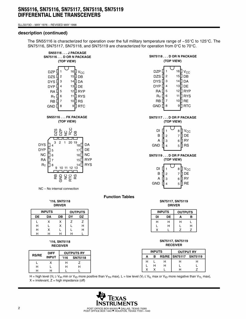
SN55116, SN75116, SN75117, SN75118, SN75119DIFFERENTIAL LINE TRANSCEIVERS
SLLS073D − MAY 1976 − REVISED MAY 1998
1POST OFFICE BOX 655303 • DALLAS, TEXAS 75265POST OFFICE BOX 1443 • HOUSTON, TEXAS 77251−1443
features common to all types
Single 5-V Supply
3-State Driver Output Circuitry
TTL-Compatible Driver Inputs
TTL-Compatible Receiver Output
Differential Line Operation
Receiver Output Strobe (SN55116,SN75116, SN75117) or Enable (SN75118,SN75119)
Designed for Party-Line (Data-Bus)Applications
additional features of the SN55116/SN75116
Choice of Ceramic or Plastic Packages
Independent Driver and Receiver
Choice of Open-Collector or Totem-PoleOutputs on Both Driver and Receiver
Dual Data Inputs on Driver
Optional Line-Termination Resistor inReceiver
±15-V Receiver Common-Mode Capability
Receiver Frequency-Response Control
additional features of the SN75117
Driver Output Internally Connected toReceiver Input
The SN75118 is an SN75116 With 3-State Receiver Output CircuitryThe SN75119 is an SN75117 With 3-State Receiver Output Circuitry
description
These integrated circuits are designed for use in interfacing between TTL-type digital systems and differentialdata-transmission lines. They are especially useful for party-line (data-bus) applications. Each of these circuittypes combine in one package a 3-state differential line driver and a differential-input line receiver, both of whichoperate from a single 5-V power supply. The driver inputs and the receiver outputs are TTL compatible. Thedriver employed is similar to the SN55113 and SN75113 3-state line drivers, and the receiver is similar to theSN55115 and SN75115 line receivers.
The SN55116, SN75116, and SN75118 offer all the features of the SN55113 and SN75113 drivers and theSN55115 and SN75115 receivers combined. The driver performs the dual input AND and NAND functions whenenabled or presents a high impedance to the load when in the disabled state. The driver output stages are similarto TTL totem-pole outputs, but have the current-sinking portion separated from the current-sourcing portion andboth are brought out to adjacent package terminals. This feature allows the user the option of using the driverin the open-collector output configuration, or, by connecting the adjacent source and sink terminals together,of using the driver in the normal totem-pole output configuration.
The receiver portion of the SN55116, SN75116, and SN75118 features a differential-input circuit having acommon-mode voltage range of ±15 V. An internal 130-Ω equivalent resistor also is provided, which optionallycan be used to terminate the transmission line. A frequency-response control terminal allows the user to reducethe speed of the receiver or to improve differential noise immunity. The receivers of the SN55116 and SN75116have an output strobe and a split totem-pole output. The receiver of the SN75118 has an output-enable for the3-state split totem-pole output. The receiver section of either circuit is independent of the driver section exceptfor the VCC and ground terminals.
The SN75117 and SN75119 provide the basic driver and receiver functions of the SN55116, SN75116, andSN75118, but use a package that is only half as large. The SN75117 and SN75119 are intended primarily forparty-line or bus-organized systems because the driver outputs are internally connected to the receiver inputs.The driver has a single data input and a single enable input. The SN75117 receiver has an output strobe, whilethe SN75119 receiver has a 3-state output enable. However, these devices do not provide output connectionoptions, line-termination resistors, or receiver frequency-response controls.
Copyright 1998, Texas Instruments IncorporatedPRODUCTION DATA information is current as of publication date.Products conform to specifications per the terms of Texas Instrumentsstandard warranty. Production processing does not necessarily includetesting of all parameters.
Please be aware that an important notice concerning availability, standard warranty, and use in critical applications ofTexas Instruments semiconductor products and disclaimers thereto appears at the end of this data sheet.
SN55116, SN75116, SN75117, SN75118, SN75119DIFFERENTIAL LINE TRANSCEIVERS
SLLS073D − MAY 1976 − REVISED MAY 1998
2 POST OFFICE BOX 655303 • DALLAS, TEXAS 75265POST OFFICE BOX 1443 • HOUSTON, TEXAS 77251−1443
description (continued)
The SN55116 is characterized for operation over the full military temperature range of −55°C to 125°C. TheSN75116, SN75117, SN75118, and SN75119 are characterized for operation from 0°C to 70°C.
1
2
3
4
5
6
7
8
16
15
14
13
12
11
10
9
DZPDZSDYSDYP
RARTRB
GND
VCCDBDADERYPRYSRSRTC
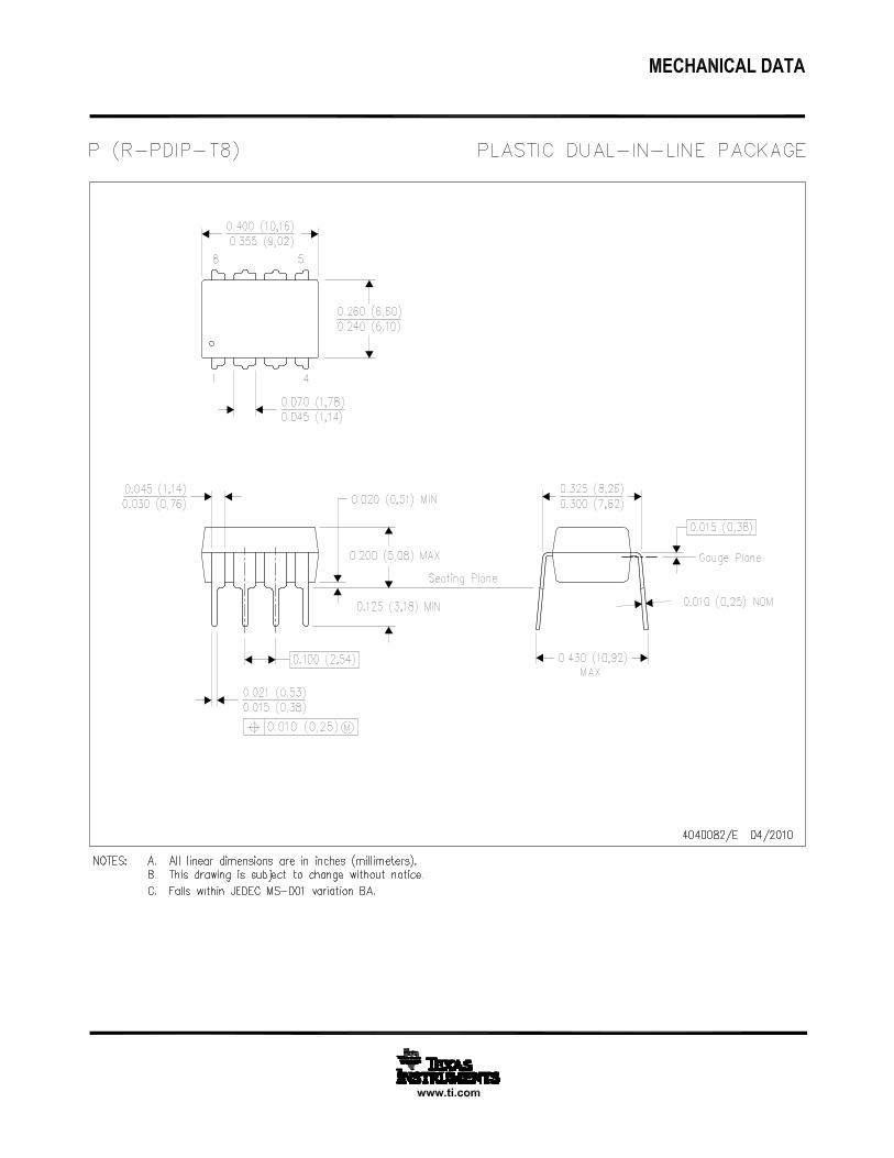
SN55116 . . . J PACKAGESN75116 . . . D OR N PACKAGE
(TOP VIEW)
1
2
3
4
5
6
7
8
16
15
14
13
12
11
10
9
DZPDZSDYSDYP
RARTRB
GND
VCCDBDADERYPRYSRERTC
SN75118 . . . D OR N PACKAGE(TOP VIEW)
3 2 1 20 19
9 10 11 12 13
4
5
6
7
8
18
17
16
15
14
DADENCRYPRYS
DYSDYP
NCRART
SN55116 . . . FK PACKAGE(TOP VIEW)
DZ
SD
ZP
NC
RS
DB
RB
GN
DN
C
NC − No internal connection
CC
VR
TC
1
2
3
4
8
7
6
5
DIBA
GND
VCCDERYRS
SN75117 . . . D OR P PACKAGE(TOP VIEW)
1
2
3
4
8
7
6
5
DIBA
GND
VCCDERYRE
SN75119 . . . D OR P PACKAGE(TOP VIEW)
Function Tables
INPUTS OUTPUTS
LHHH
’116, SN75118DRIVER
DE DA DB
XLXH
XXLH
DY DZ
ZLLH
ZHHL
INPUTS OUTPUTS
SN75117, SN75119DRIVER
DI DE
HLX
HHL
A B
HLZ
LHZ
OUTPUTS RY
’116, SN75118RECEIVER
RS/REDIFF
INPUT
LHH
XLH
’116 SN75118
HHL
ZHL
INPUTS OUTPUT RY
SN75117, SN75119RECEIVER
B RS/RE
LHX
HHL
SN75117 SN75119
HLH
HLZ
A
HLX
H = high level (VI ≥ VIH min or VID more positive than VTH max), L = low level (VI ≤ VIL max or VID more negative than VTL max),X = irrelevant, Z = high impedance (off)

SN55116, SN75116, SN75117, SN75118, SN75119DIFFERENTIAL LINE TRANSCEIVERS
SLLS073D − MAY 1976 − REVISED MAY 1998
3POST OFFICE BOX 655303 • DALLAS, TEXAS 75265POST OFFICE BOX 1443 • HOUSTON, TEXAS 77251−1443
logic symbol†
EN
B
A
6
5
1
7
RY
RS
DI
DE2
3
&
&
&
RESP
RT
EN
9
10
6
5
7
15
14
13
RYS
RYP
DZS
DZP
DYS
DYP
RTC
RS
RT
RA
RB
DB
DA
DE
11
12
2
1
3
4
’116‡
&
RESP
RT
EN
9
10
6
5
7
15
14
13
RYS
RYP
DZS
DZP
DYS
DYP
RTC
RE
RT
RA
RB
DB
DA
DE
11
12
2
1
3
4
SN75118‡
EN
SN75117‡
EN
B
A
6
5
1
7
RY
RE
DI
DE2
3
SN75119‡
EN
5
logic diagram (positive logic)
6
3
2
5
7
1
RE
DE
DI RY
A
BBUS
BUSB
A
RYDI
DE
RS
1
7
5
2
3
6
RTC
RT
RA
RB
RE
9
6
5
7
10
RYP (pullup)
RYS (sink)
12
11
RS
RTC
RT
RA
RB
10
9
6
7
RYS (sink)
RYP (pullup)11
12
DB
DA
DE
15
14
13
DZS (sink)
DZP (pullup)
DYS (sink)
DYP (pullup)
2
1
3
4
’116 and SN75118‡
’116 Receiver‡
SN75118 Receiver‡
SN75119 Driver and Receiver‡
SN75117 Driver and Receiver‡
† These symbols are in accordance with ANSI/IEEE Std 91-1984 and IEC Publication 617-12.‡ Pin numbers shown for the SN55116 and SN75116 are for the D, J, and N packages, those shown for the SN75118 are for the D and N packages,
and those shown for SN75117 and SN75119 are for the D and P packages.

SN55116, SN75116, SN75117, SN75118, SN75119DIFFERENTIAL LINE TRANSCEIVERS
SLLS073D − MAY 1976 − REVISED MAY 1998
4 POST OFFICE BOX 655303 • DALLAS, TEXAS 75265POST OFFICE BOX 1443 • HOUSTON, TEXAS 77251−1443
schematics of inputs and outputs
7 kΩNOM
EQUIVALENT OFEACH DRIVER INPUT
AND EACH RE AND RS INPUT
VCC
Input
4 kΩNOM
EQUIVALENT OFEACH RECEIVER INPUT
(EXCLUDING ENABLES AND STROBES)
VCC1 pF NOM
Input8 kΩNOM
130 ΩNOM
TYPICAL OF ALL OUTPUTS
VCC
RPullupoutput†
Driver output R = 9 Ω NOMReceiver output R = 20 Ω NOM
Sinkoutput†
† On SN75117 and SN75119, common outputsreplace the separate pullup and sink outputs.
absolute maximum ratings over operating free-air temperature (unless otherwise noted)‡
Supply voltage, VCC (see Notes 1 and 2) 7 V. . . . . . . . . . . . . . . . . . . . . . . . . . . . . . . . . . . . . . . . . . . . . . . . . . . . . . . Input voltage, VI: DA, DB, DE, DI, RE, and RS 5.5 V. . . . . . . . . . . . . . . . . . . . . . . . . . . . . . . . . . . . . . . . . . . . . . . .
RA, RB, RT for ’116, SN75118 only ±25 V. . . . . . . . . . . . . . . . . . . . . . . . . . . . . . . . . . . . . . . . . . A and B for SN75117, SN75119 only 0 to 6 V. . . . . . . . . . . . . . . . . . . . . . . . . . . . . . . . . . . . . . .
Off-state voltage applied to open-collector outputs: ’116, SN75118 only 12 V. . . . . . . . . . . . . . . . . . . . . . . . . . . Continuous total power dissipation (see Note 2) See Dissipation Rating Table. . . . . . . . . . . . . . . . . . . . . . . . . . Storage temperature range, Tstg −65°C to 150°C. . . . . . . . . . . . . . . . . . . . . . . . . . . . . . . . . . . . . . . . . . . . . . . . . . . Case temperature for 60 seconds, TC: FK package 260°C. . . . . . . . . . . . . . . . . . . . . . . . . . . . . . . . . . . . . . . . . . . Lead temperature 1,6 mm (1/16 inch) from case for 60 seconds: J package 300°C. . . . . . . . . . . . . . . . . . . . . Lead temperature 1,6 mm (1/16 inch) from case for 10 seconds: D, N, or P package 260°C. . . . . . . . . . . . .
‡ Stresses beyond those listed under “absolute maximum ratings” may cause permanent damage to the device. These are stress ratings only, andfunctional operation of the device at these or any other conditions beyond those indicated under “recommended operating conditions” is notimplied. Exposure to absolute-maximum-rated conditions for extended periods may affect device reliability.
NOTES: 1. All voltage values are with respect to the network ground terminal.2. In the FK and J packages, the SN55116 chip is alloy mounted. The SN75116, SN75117, SN75118, and SN75119 chips are glass
mounted.

SN55116, SN75116, SN75117, SN75118, SN75119DIFFERENTIAL LINE TRANSCEIVERS
SLLS073D − MAY 1976 − REVISED MAY 1998
5POST OFFICE BOX 655303 • DALLAS, TEXAS 75265POST OFFICE BOX 1443 • HOUSTON, TEXAS 77251−1443
DISSIPATION RATING TABLE
PACKAGETA ≤ 25°C
POWER RATINGDERATING FACTOR
ABOVE TA = 25°CTA = 70°C
POWER RATINGTA = 125°C
POWER RATING
D (8 pin) 725 mW 5.8 mW/°C 464 mW —
D (16 pin) 950 mW 7.6 mW/°C 608 mW —
FK 1375 mW 11.0 mW/°C 880 mW 275 mW
J 1375 mW 11.0 mW/°C 880 mW 275 mW
N 1150 mW 9.2 mW/°C 736 mW —
P 1000 mW 8.0 mW/°C 640 mW —
recommended operating conditions
PARAMETERSN55116 SN75116, SN75117,
SN75118, SN75119 UNITPARAMETERMIN NOM MAX MIN NOM MAX
UNIT
Supply voltage, VCC 4.5 5 5.5 4.5 5 5.5 V
High-level input voltage, VIH All inputs except differential 2 2 V
Low-level input voltage, VIL
All inputs except differentialinputs 0.8 0.8 V
High level output current IDrivers −40 −40
mAHigh-level output current, IOH Receivers −5 −5mA
Low level output current IDrivers 40 40
mALow-level output current, IOL Receivers 15 15mA
Receiver input voltage V’116, SN75118 ±15 ±15
VReceiver input voltage, VI SN75117, SN75119 0 6 0 6V
Common mode receiver input voltage V’116, SN75118 ±15 ±15
VCommon-mode receiver input voltage, VICR SN75117, SN75119 0 6 0 6V
Operating free-air temperature, TA −55 125 0 70 °C
SN
55116, SN
75116, SN
75117, SN
75118, SN
75119D
IFF
ER
EN
TIA
L L
INE
TR
AN
SC
EIV
ER
S
SLLS
073D −
MA
Y 1976 −
RE
VIS
ED
MA
Y 1998
6P
OS
T O
FF
ICE
BO
X 655303 D
ALLA
S, T
EX
AS
75265•
PO
ST
OF
FIC
E B
OX
1443 HO
US
TO
N, T
EX
AS
77251−1443
•
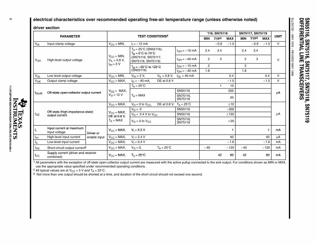
electrical characteristics over recommended operating free-air temperature range (unless otherwise noted)
driver section
PARAMETER TEST CONDITIONS†’116, SN75118 SN75117, SN75119
UNITPARAMETER TEST CONDITIONS†MIN TYP‡ MAX MIN TYP‡ MAX
UNIT
VIK Input clamp voltage VCC = MIN, II = −12 mA −0.9 −1.5 −0.9 −1.5 V
TA = 25°C (SN55116), TA = 0°C to 70°C
IOH = −10 mA 2.4 3.4 2.4 3.4
VOH High-level output voltageVCC = MIN,VIL = 0.8 V,I 2 V
TA = 0 C to 70 C (SN75116, SN75117,SN75118, SN75119)
IOH = −40 mA 2 3 2 3 VIIH = 2 V
TA = −55°C to 125°C IOH = −10 mA 2 2TA = −55 C to 125 C(SN55116) IOH = −40 mA 1.8 1.8
VOL Low-level output voltage VCC = MIN, VIH = 2 V, VIL = 0.8 V, IOL = 40 mA 0.4 0.4 V
VOK Output clamp voltage VCC = MAX, IO = −40 mA, DE at 0.8 V −1.5 −1.5 V
TA = 25°C 1 10
IO(off) Off-state open-collector output currentVCC = MAX, SN55116 200 µAIO(off) Off-state open-collector output current CC ,VO = 12 V TA = MAX SN75116,
SN75118 20
µA
VCC = MAX, VO = 0 to VCC, DE at 0.8 V, TA = 25°C ±10
Off state (high impedance state) V MAXVO = 0 SN55116 −300
IOZOff-state (high-impedance-state)output current
VCC = MAX,DE at 0 8 V
VO = 0.4 V to VCC SN55116 ±150 µAOZ output current DE at 0.8 V,TA = MAX VO = 0 to VCC
SN75116,SN75118 ±20
µ
IInput current at maximum
V = MAX V = 5 5 V 1 1 mAIIInput current at maximuminput voltage Driver or
VCC = MAX, VI = 5.5 V 1 1 mA
IIH High-level input currentDriver orenable input VCC = MAX, VI = 2.4 V 40 40 µA
IIL Low-level input current
enable input
VCC = MAX, VI = 0.4 V −1.6 −1.6 mA
IOS Short-circuit output current§ VCC = MAX, VO = 0, TA = 25°C −40 −120 −40 −120 mA
ISupply current (driver and receiver
V = MAX T = 25°C 42 60 42 60 mAICCSupply current (driver and receivercombined) VCC = MAX, TA = 25°C 42 60 42 60 mA
† All parameters with the exception of off-state open-collector output current are measured with the active pullup connected to the sink output. For conditions shown as MIN or MAX,use the appropriate value specified under recommended operating conditions.
‡ All typical values are at VCC = 5 V and TA = 25°C.§ Not more than one output should be shorted at a time, and duration of the short circuit should not exceed one second.
SN55116, SN75116, SN75117, SN75118, SN75119DIFFERENTIAL LINE TRANSCEIVERS
SLLS073D − MAY 1976 − REVISED MAY 1998
7POST OFFICE BOX 655303 • DALLAS, TEXAS 75265POST OFFICE BOX 1443 • HOUSTON, TEXAS 77251−1443
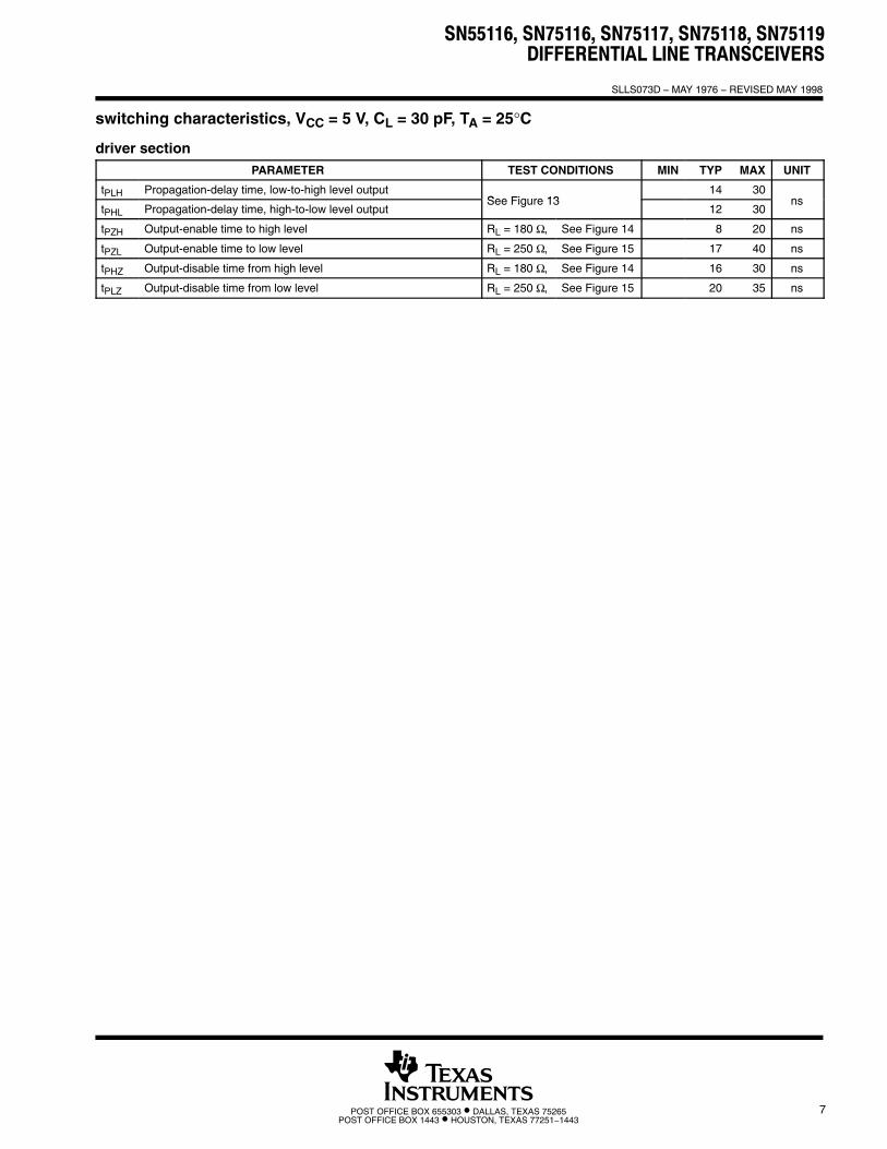
switching characteristics, VCC = 5 V, CL = 30 pF, TA = 25°C
driver sectionPARAMETER TEST CONDITIONS MIN TYP MAX UNIT
tPLH Propagation-delay time, low-to-high level outputSee Figure 13
14 30ns
tPHL Propagation-delay time, high-to-low level outputSee Figure 13
12 30ns
tPZH Output-enable time to high level RL = 180 Ω, See Figure 14 8 20 ns
tPZL Output-enable time to low level RL = 250 Ω, See Figure 15 17 40 ns
tPHZ Output-disable time from high level RL = 180 Ω, See Figure 14 16 30 ns
tPLZ Output-disable time from low level RL = 250 Ω, See Figure 15 20 35 ns
SN
55116, SN
75116, SN
75117, SN
75118, SN
75119D
IFF
ER
EN
TIA
L L
INE
TR
AN
SC
EIV
ER
S
SLLS
073D −
MA
Y 1976 −
RE
VIS
ED
MA
Y 1998
8P
OS
T O
FF
ICE
BO
X 655303 D
ALLA
S, T
EX
AS
75265•
PO
ST
OF
FIC
E B
OX
1443 HO
US
TO
N, T
EX
AS
77251−1443
•
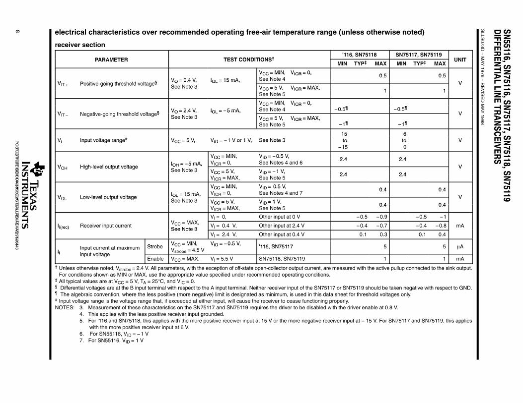
electrical characteristics over recommended operating free-air temperature range (unless otherwise noted)
receiver section
PARAMETER TEST CONDITIONS†’116, SN75118 SN75117, SN75119
UNITPARAMETER TEST CONDITIONS†MIN TYP‡ MAX MIN TYP‡ MAX
UNIT
VCC = MIN, VICR = 0,0 5 0 5
V Positive going threshold voltage§ VO = 0.4 V, IOL = 15 mA,VCC = MIN, VICR = 0,See Note 4
0.5 0.5VVIT + Positive-going threshold voltage§ VO = 0.4 V,
See Note 3IOL = 15 mA,
VCC = 5 V, VICR = MAX,1 1
VSee Note 3 VCC = 5 V, VICR = MAX,
See Note 51 1
VCC = MIN, VICR = 0,
V Negative going threshold voltage§ VO = 2.4 V, IOL = −5 mA,VCC = MIN, VICR = 0,See Note 4 −0.5¶ −0.5¶
VVIT − Negative-going threshold voltage§ VO = 2.4 V,See Note 3
IOL = 5 mA,VCC = 5 V, VICR = MAX,
VSee Note 3 VCC = 5 V, VICR = MAX,
See Note 5 −1¶ −1¶
15 6VI Input voltage range# VCC = 5 V, VID = −1 V or 1 V, See Note 3
15to
6to VVI Input voltage range VCC 5 V, VID 1 V or 1 V, See Note 3 to
−15 to
0 V
VCC = MIN, VID = −0.5 V,2 4 2 4
V High level output voltageIOH = −5 mA,
VCC = MIN,VICR = 0,
VID = 0.5 V,See Notes 4 and 6
2.4 2.4VVOH High-level output voltage
IOH = 5 mA,See Note 3 VCC = 5 V, VID = −1 V,
2 4 2 4V
See Note 3 VCC = 5 V,VICR = MAX,
VID = 1 V,See Note 5
2.4 2.4
VCC = MIN, VID = 0.5 V,0 4 0 4
V Low level output voltageIOL = 15 mA,
VCC = MIN,VICR = 0,
VID = 0.5 V,See Notes 4 and 7
0.4 0.4VVOL Low-level output voltage
IOL = 15 mA,See Note 3 VCC = 5 V, VID = 1 V,
0 4 0 4V
See Note 3 VCC = 5 V,VICR = MAX,
VID = 1 V,See Note 5
0.4 0.4
V MAXVI = 0, Other input at 0 V −0.5 −0.9 −0.5 −1
II(rec) Receiver input currentVCC = MAX,See Note 3
VI = 0.4 V, Other input at 2.4 V −0.4 −0.7 −0.4 −0.8 mAI(rec) pSee Note 3
VI = 2.4 V, Other input at 0.4 V 0.1 0.3 0.1 0.4
I t t t i StrobeVCC = MIN, VID = −0.5 V,
’116 SN75117 5 5 µAII
Input current at maximuminput voltage
StrobeVCC = MIN, VID = 0.5 V,Vstrobe = 4.5 V
’116, SN75117 5 5 µAII input voltage
Enable VCC = MAX, VI = 5.5 V SN75118, SN75119 1 1 mA
† Unless otherwise noted, Vstrobe = 2.4 V. All parameters, with the exception of off-state open-collector output current, are measured with the active pullup connected to the sink output.For conditions shown as MIN or MAX, use the appropriate value specified under recommended operating conditions.
‡ All typical values are at VCC = 5 V, TA = 25°C, and VIC = 0.§ Differential voltages are at the B input terminal with respect to the A input terminal. Neither receiver input of the SN75117 or SN75119 should be taken negative with respect to GND.¶ The algebraic convention, where the less positive (more negative) limit is designated as minimum, is used in this data sheet for threshold voltages only.# Input voltage range is the voltage range that, if exceeded at either input, will cause the receiver to cease functioning properly.NOTES: 3. Measurement of these characteristics on the SN75117 and SN75119 requires the driver to be disabled with the driver enable at 0.8 V.
4. This applies with the less positive receiver input grounded.5. For ’116 and SN75118, this applies with the more positive receiver input at 15 V or the more negative receiver input at − 15 V. For SN75117 and SN75119, this applies
with the more positive receiver input at 6 V.6. For SN55116, VID = −1 V7. For SN55116, VID = 1 V
SN
55116, SN
75116, SN
75117, SN
75118, SN
75119D
IFF
ER
EN
TIA
L L
INE
TR
AN
SC
EIV
ER
S
SLLS
073D −
MA
Y 1976 −
RE
VIS
ED
MA
Y 1998
PO
ST
OF
FIC
E B
OX
655303 DA
LLAS
, TE
XA
S 75265
•P
OS
T O
FF
ICE
BO
X 1443 H
OU
ST
ON
, TE
XA
S 77251−
1443•
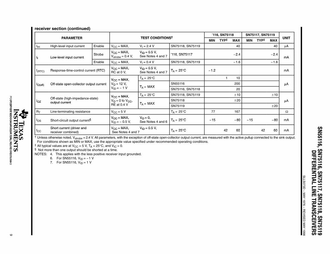
9
receiver section (continued)
PARAMETER TEST CONDITIONS†’116, SN75118 SN75117, SN75119
UNITPARAMETER TEST CONDITIONS†MIN TYP‡ MAX MIN TYP‡ MAX
UNIT
IIH High-level input current Enable VCC = MAX, VI = 2.4 V SN75118, SN75119 40 40 µA
StrobeVCC = MAX, VID = 0.5 V,
’116 SN75117 2 4 2 4II Low-level input current
StrobeVCC = MAX,Vstrobe = 0.4 V,
VID = 0.5 V,See Notes 4 and 7 ’116, SN75117 −2.4 −2.4
mAII Low level input current
Enable VCC = MAX, VI = 0.4 V SN75118, SN75119 −1.6 −1.6
mA
I Response time control current (RTC)VCC = MAX, VID = 0.5 V,
T 25°C 1 2 mAI(RTC) Response-time-control current (RTC)VCC = MAX,RC at 0 V,
VID = 0.5 V,See Notes 4 and 7 TA = 25°C −1.2 mA
VCC = MAX, TA = 25°C 1 10
IO(off) Off-state open-collector output currentVCC = MAX,VO = 12 V,
T MAXSN55116 200 µAIO(off) Off state open collector output current VO 12 V,
VID = − 1 V TA = MAXSN75116, SN75118 20
µA
Off t t (hi h i d t t )VCC = MAX, TA = 25°C SN75118, SN75119 ±10 ±10
IOZOff-state (high-impedance-state)output current
VCC = MAX,VO = 0 to VCC,
T MAXSN75118 ±20 µAIOZ output current
VO 0 to VCC,RE at 0.4 V TA = MAX
SN75119 ±20
µA
RT Line-terminating resistance VCC = 5 V TA = 25°C 77 167 Ω
I Sh t i it t t t§VCC = MAX, VO = 0,
T 25°C 15 80 15 80 mAIOS Short-circuit output current§VCC = MAX,VID = − 0.5 V,
VO = 0,See Notes 4 and 6 TA = 25°C −15 −80 −15 −80 mA
IShort current (driver and VCC = MAX, VID = 0.5 V,
T 25°C 42 60 42 60 mAICCShort current (driver andreceiver combined)
VCC = MAX, VID = 0.5 V, See Notes 4 and 7 TA = 25°C 42 60 42 60 mA
† Unless otherwise noted, Vstrobe = 2.4 V. All parameters, with the exception of off-state open-collector output current, are measured with the active pullup connected to the sink output.For conditions shown as MIN or MAX, use the appropriate value specified under recommended operating conditions.
‡ All typical values are at VCC = 5 V, TA = 25°C, and VIC = 0.§ Not more than one output should be shorted at a time.NOTES: 4. This applies with the less positive receiver input grounded.
6. For SN55116, VID = −1 V7. For SN55116, VID = 1 V
SN55116, SN75116, SN75117, SN75118, SN75119DIFFERENTIAL LINE TRANSCEIVERS
SLLS073D − MAY 1976 − REVISED MAY 1998
11POST OFFICE BOX 655303 • DALLAS, TEXAS 75265POST OFFICE BOX 1443 • HOUSTON, TEXAS 77251−1443
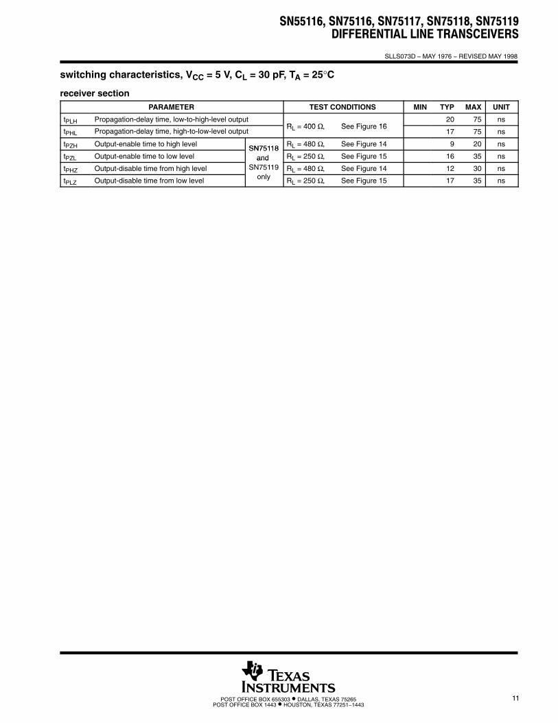
switching characteristics, VCC = 5 V, CL = 30 pF, TA = 25°C
receiver sectionPARAMETER TEST CONDITIONS MIN TYP MAX UNIT
tPLH Propagation-delay time, low-to-high-level outputR 400 Ω See Figure 16
20 75 ns
tPHL Propagation-delay time, high-to-low-level outputRL = 400 Ω, See Figure 16
17 75 ns
tPZH Output-enable time to high levelSN75118
RL = 480 Ω, See Figure 14 9 20 ns
tPZL Output-enable time to low levelSN75118
and RL = 250 Ω, See Figure 15 16 35 ns
tPHZ Output-disable time from high level
and SN75119
lRL = 480 Ω, See Figure 14 12 30 ns
tPLZ Output-disable time from low level only RL = 250 Ω, See Figure 15 17 35 ns
SN55116, SN75116, SN75117, SN75118, SN75119DIFFERENTIAL LINE TRANSCEIVERS
SLLS073D − MAY 1976 − REVISED MAY 1998
12 POST OFFICE BOX 655303 • DALLAS, TEXAS 75265POST OFFICE BOX 1443 • HOUSTON, TEXAS 77251−1443
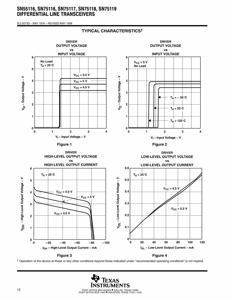
TYPICAL CHARACTERISTICS†
Figure 1
ÁÁÁÁÁÁÁÁ
3
2
1
00 1 2
4
5
6
3 4
DRIVEROUTPUT VOLTAGE
vsINPUT VOLTAGE
VI − Input Voltage − V
ÎÎÎÎÎÎÎÎÎÎ
VCC = 5.5 V
ÎÎÎÎÎÎÎÎ
VCC = 5 V
ÎÎÎÎÎÎÎÎÎÎ
VCC = 4.5 V
ÁÁÁÁÁÁÁÁ
No LoadTA = 25°C
VO
− O
utp
ut
Volt
age
− V
ÁÁÁÁ
VO
Figure 2
3
2
1
00 1 2
4
5
6
3 4
DRIVEROUTPUT VOLTAGE
vsINPUT VOLTAGE
VI − Input Voltage − V
ÎÎÎÎÎÎÎÎÎÎÎÎ
TA = − 55°C
ÎÎÎÎÎÎÎÎÎÎ
TA = 125°C
ÎÎÎÎÎÎÎÎÎÎ
TA = 25°C
ÁÁÁÁÁÁÁÁÁÁÎÎÎÎÎÎÎÎÎÎ
VCC = 5 VNo Load
VO
− O
utp
ut
Volt
age
− V
ÁÁÁÁÁÁ
VO
Figure 3
0
VO
H −
Hig
h-L
evel
Ou
tpu
t Vo
ltag
e −
V
IOH − High-Level Output Current − mA
6
−1000
−20 −40 −60 −80
1
2
3
4
5
TA = 25°C
ÎÎÎÎÎÎÎÎ
VCC = 5 V
VCC = 4.5 V
DRIVERHIGH-LEVEL OUTPUT VOLTAGE
vsHIGH-LEVEL OUTPUT CURRENT
ÁÁÁÁV
OH
ÎÎÎÎÎÎÎÎÎÎ
VCC = 5.5 V
Figure 4
0.3
0.2
0.1
00 20 40
0.4
0.5
0.6
50 80 100 120
ÎÎÎÎÎVCC = 4.5 V
ÎÎÎÎÎÎÎÎ
VCC = 5.5 V
VO
L −
Lo
w-L
evel
Ou
tpu
t Vo
ltag
e −
V
IOL − Low-Level Output Current − mA
DRIVERLOW-LEVEL OUTPUT VOLTAGE
vsLOW-LEVEL OUTPUT CURRENT
ÎÎÎÎÎÎÎÎ
TA = 25°C
ÁÁÁÁ
VO
L
† Operation of the device at these or any other conditions beyond those indicated under ‘‘recommended operating conditions” is not implied.

SN55116, SN75116, SN75117, SN75118, SN75119DIFFERENTIAL LINE TRANSCEIVERS
SLLS073D − MAY 1976 − REVISED MAY 1998
13POST OFFICE BOX 655303 • DALLAS, TEXAS 75265POST OFFICE BOX 1443 • HOUSTON, TEXAS 77251−1443
TYPICAL CHARACTERISTICS†
Figure 5
− P
rop
agat
ion
Del
ay T
ime
− n
s
DRIVERPROPAGATION-DELAY TIME
vsFREE-AIR TEMPERATURE
TA − Free-Air Temperature − °C
10
8
4
2
0
18
6
14
12
16
20
−75 0 25 50 75 100 125
ÎÎÎÎÎÎ
tPLH
ÎÎÎÎÎÎ
tPHL
ÁÁÁÁÁÁÁÁÁÁÁÁ
ÎÎÎÎVCC = 5 V
ÎÎÎÎÎÎÎÎSee Figure 13
ÎÎÎÎÎÎÎÎCL = 30 pF
−50 −25
t pd
Figure 6
Ou
tpu
t E
nab
le a
nd
Dis
able
Tim
e −
ns
20
10
5
0
25
15
30
−75 0 25 50 75 100 125
TA − Free-Air Temperature − °C
ÎÎÎÎÎÎ
tPLZ
ÎÎÎÎÎÎ
tPZH
ÎÎÎÎÎÎ
tPHZÎÎÎtPZL
DRIVEROUTPUT-ENABLE AND DISABLE TIME
vsFREE-AIR TEMPERATURE
ÁÁÁÁÁÁÁÁÁÁÁÁÁÁÁÎÎÎÎÎÎÎÎ
See Note AÎÎÎÎVCC = 5 V
−50 −25
NOTE A: For tPZH and tPHZ: RL = 480 Ω, see Figure 14. For tPZLand tPLZ: RL = 250 Ω, see Figure 15.
Figure 7
VCC = 5.5 V ÁÁÁÁÁÁÁÁÁÁÁÁÁÁÁÁÁÁÁÁÁ
RECEIVEROUTPUT VOLTAGE
vsDIFFERENTIAL INPUT VOLTAGE
−0.2
VO
− O
utp
ut
Volt
age
− V
VID − Differential Input Voltage − V
6
0.20
−0.1 0 0.1
1
2
3
4
5VCC = 4.5 V
Load = 2 kΩ to VCCTA = 25°C
ÁÁÁÁÁÁV
O
ÎÎÎÎÎÎÎÎ
VCC = 5 V
Figure 8
RECEIVEROUTPUT VOLTAGE
vsDIFFERENTIAL INPUT VOLTAGE
−0.2
VO
− O
utp
ut
Volt
age
− V
6
0.20
−0.1 0 0.1
1
2
3
4
5
VID − Differential Input Voltage − V
ÎÎÎÎÎÎÎÎ
TA = 25°C
ÎÎÎÎÎÎÎÎ
TA = 125°C
ÎÎÎÎÎÎÎÎ
TA = −55°C
ÁÁÁÁÁÁÁÁÁÁÁÁÁÁÁÁÁÁÎÎÎÎÎÎVCC = 5 VÎÎÎÎÎÎÎÎÎÎÎÎÎÎ
Load = 2 kΩ to VCC
ÁÁÁÁV
O
† Operation of the device at these or any other conditions beyond those indicated under ‘‘recommended operating conditions” is not implied.

SN55116, SN75116, SN75117, SN75118, SN75119DIFFERENTIAL LINE TRANSCEIVERS
SLLS073D − MAY 1976 − REVISED MAY 1998
14 POST OFFICE BOX 655303 • DALLAS, TEXAS 75265POST OFFICE BOX 1443 • HOUSTON, TEXAS 77251−1443
TYPICAL CHARACTERISTICS†
Figure 9
RECEIVERPROPAGATION-DELAY TIME
vsFREE-AIR TEMPERATURE
TA − Free-Air Temperature − °C
ÎÎÎÎÎÎ
tPLH
ÎÎÎÎ
tPHL
20
10
5
0
25
15
30
−75 0 25 50 75 100 125
ÁÁÁÁÁÁÁÁÁÁÁÁÁÁÁ
ÎÎÎÎÎÎÎÎ
VCC = 5 V
ÎÎÎÎÎRL = 400 ΩÎÎÎÎÎÎÎÎÎÎ
See Figure 16
−50 −25
− P
rop
agat
ion
Del
ay T
ime
− n
s t p
d
Figure 10
Ou
tpu
t E
nab
le a
nd
Dis
able
Tim
e −
ns
20
10
5
0
25
15
30
−75 0 25 50 75 100 125
TA − Free-Air Temperature − °C
ÎÎÎtPLZ
ÎÎÎtPZH
ÎÎÎÎÎÎ
tPHZ
ÎÎÎÎÎÎ
tPZL
RECEIVEROUTPUT-ENABLE AND DISABLE TIME
vsFREE-AIR TEMPERATURE
ÁÁÁÁÁÁÁÁÁÁÁÁÎÎÎÎÎÎÎÎ
See Note AÎÎÎÎVCC = 5 V
−50 −25
NOTE A: For tPZH and tPHZ :RL= 480 Ω, see Figure 14. For tPZLand tPLZ: RL = 250 Ω, see Figure 15.
Figure 11
40
20
10
00 1 2 3 4 5
60
70
80
6 7 8
50
30
ICC
− S
up
ply
Cu
rren
t −
mA
VCC − Supply Voltage − V
DRIVER AND RECEIVERSUPPLY CURRENT
vsSUPPLY VOLTAGE
ÁÁÁÁÁÁÁÁÎÎÎÎNo LoadÎÎÎÎÎÎÎÎÎÎ
TA = 25°C
ÁÁÁÁ
CC
I
Figure 12
DRIVER AND RECEIVERSUPPLY CURRENT
vsFREE-AIR TEMPERATURE
ICC
− S
up
ply
Cu
rren
t −
mA
TA − Free-Air Temperature − °C
ÎÎÎÎVCC = 5 V
25
20
10
5
0
45
15
35
30
40
50
−75 0 25 50 75 100 125
ÁÁÁÁÁÁ
CC
I
−50 −25
† Operation of the device at these or any other conditions beyond those indicated under ‘‘recommended operating conditions” is not implied.
SN55116, SN75116, SN75117, SN75118, SN75119DIFFERENTIAL LINE TRANSCEIVERS
SLLS073D − MAY 1976 − REVISED MAY 1998
15POST OFFICE BOX 655303 • DALLAS, TEXAS 75265POST OFFICE BOX 1443 • HOUSTON, TEXAS 77251−1443
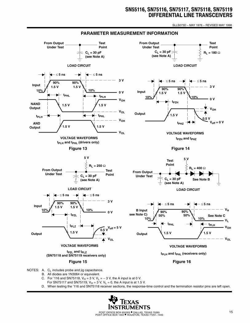
PARAMETER MEASUREMENT INFORMATION
Figure 13
From OutputUnder Test
TestPoint
CL = 30 pF(see Note A)
LOAD CIRCUIT
≤ 5 ns
Input
10%
90%1.5 V
3 V
0 V
NANDOutput
ANDOutput
tPLH tPHL
VOLTAGE WAVEFORMS
VOH
VOL
VOH
VOL
tPHL tPLH
1.5 V
1.5 V
90%
10%
≤ 5 ns
1.5 V
1.5 V 1.5 V
tPLH and tPHL (drivers only)
Figure 14
RL = 180 Ω
3 V
0 V
0.5 V
tPZH
VOH
Voff = 0 VtPHZ
Input
Output
VOLTAGE WAVEFORMS
LOAD CIRCUIT
From OutputUnder Test
CL = 30 pF(see Note A)
TestPoint
≤ 5 ns ≤ 5 ns
90% 90%1.5 V 1.5 V
10% 10%
1.5 V
tPZH and tPHZ
Figure 15
From OutputUnder Test
TestPointCL = 30 pF
(see Note A)
RL = 250 Ω
5 V
VOLTAGE WAVEFORMS
LOAD CIRCUIT
VOL
Voff = 5 V0.5 V
1.5 V10% 10%
90% 90%
≤ 5 ns
0 V
3 V
1.5 V
tPZL
tPLZ
Input
Output
≤ 5 ns
1.5 V
tPZL and tPLZ(SN75118 and SN75119 receivers only)
Figure 16
RL = 400 Ω
5 V
See Note B
LOAD CIRCUIT
VOLTAGE WAVEFORMS
Output
10% 10%See Note C
VL
VH
VOH
VOL
tPHL tPLH
B Input(see Note C)
TestPoint
From OutputUnder Test
CL = 30 pF(see Note A)
≤ 5 ns ≤ 5 ns
90%50%
90%50%
1.5 V 1.5 V
tPLH and tPHL (receivers only)
NOTES: A. CL includes probe and jig capacitance.B. All diodes are 1N3064 or equivalent.C. For ’116 and SN75118, VH = 3 V, VL = − 3 V, the A input is at 0 V.
For SN75117 and SN75119, VH = 3 V, VL = 0, the A input is at 1.5 V.D. When testing the ’116 and SN75118 receiver sections, the response-time control and the termination resistor pins are left open.
PACKAGE OPTION ADDENDUM
www.ti.com 5-Sep-2011
Addendum-Page 1
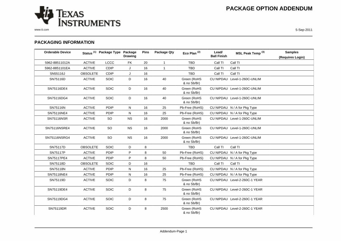
PACKAGING INFORMATION
Orderable Device Status (1) Package Type PackageDrawing
Pins Package Qty Eco Plan (2) Lead/Ball Finish
MSL Peak Temp (3) Samples
(Requires Login)
5962-88511012A ACTIVE LCCC FK 20 1 TBD Call TI Call TI
5962-8851101EA ACTIVE CDIP J 16 1 TBD Call TI Call TI
SN55116J OBSOLETE CDIP J 16 TBD Call TI Call TI
SN75116D ACTIVE SOIC D 16 40 Green (RoHS& no Sb/Br)
CU NIPDAU Level-1-260C-UNLIM
SN75116DE4 ACTIVE SOIC D 16 40 Green (RoHS& no Sb/Br)
CU NIPDAU Level-1-260C-UNLIM
SN75116DG4 ACTIVE SOIC D 16 40 Green (RoHS& no Sb/Br)
CU NIPDAU Level-1-260C-UNLIM
SN75116N ACTIVE PDIP N 16 25 Pb-Free (RoHS) CU NIPDAU N / A for Pkg Type
SN75116NE4 ACTIVE PDIP N 16 25 Pb-Free (RoHS) CU NIPDAU N / A for Pkg Type
SN75116NSR ACTIVE SO NS 16 2000 Green (RoHS& no Sb/Br)
CU NIPDAU Level-1-260C-UNLIM
SN75116NSRE4 ACTIVE SO NS 16 2000 Green (RoHS& no Sb/Br)
CU NIPDAU Level-1-260C-UNLIM
SN75116NSRG4 ACTIVE SO NS 16 2000 Green (RoHS& no Sb/Br)
CU NIPDAU Level-1-260C-UNLIM
SN75117D OBSOLETE SOIC D 8 TBD Call TI Call TI
SN75117P ACTIVE PDIP P 8 50 Pb-Free (RoHS) CU NIPDAU N / A for Pkg Type
SN75117PE4 ACTIVE PDIP P 8 50 Pb-Free (RoHS) CU NIPDAU N / A for Pkg Type
SN75118D OBSOLETE SOIC D 16 TBD Call TI Call TI
SN75118N ACTIVE PDIP N 16 25 Pb-Free (RoHS) CU NIPDAU N / A for Pkg Type
SN75118NE4 ACTIVE PDIP N 16 25 Pb-Free (RoHS) CU NIPDAU N / A for Pkg Type
SN75119D ACTIVE SOIC D 8 75 Green (RoHS& no Sb/Br)
CU NIPDAU Level-2-260C-1 YEAR
SN75119DE4 ACTIVE SOIC D 8 75 Green (RoHS& no Sb/Br)
CU NIPDAU Level-2-260C-1 YEAR
SN75119DG4 ACTIVE SOIC D 8 75 Green (RoHS& no Sb/Br)
CU NIPDAU Level-2-260C-1 YEAR
SN75119DR ACTIVE SOIC D 8 2500 Green (RoHS& no Sb/Br)
CU NIPDAU Level-2-260C-1 YEAR

PACKAGE OPTION ADDENDUM
www.ti.com 5-Sep-2011
Addendum-Page 2
Orderable Device Status (1) Package Type PackageDrawing
Pins Package Qty Eco Plan (2) Lead/Ball Finish
MSL Peak Temp (3) Samples
(Requires Login)
SN75119DRE4 ACTIVE SOIC D 8 2500 Green (RoHS& no Sb/Br)
CU NIPDAU Level-2-260C-1 YEAR
SN75119DRG4 ACTIVE SOIC D 8 2500 Green (RoHS& no Sb/Br)
CU NIPDAU Level-2-260C-1 YEAR
SN75119P ACTIVE PDIP P 8 50 Pb-Free (RoHS) CU NIPDAU N / A for Pkg Type
SN75119PE4 ACTIVE PDIP P 8 50 Pb-Free (RoHS) CU NIPDAU N / A for Pkg Type
SNJ55116FK ACTIVE LCCC FK 20 1 TBD POST-PLATE N / A for Pkg Type
SNJ55116J ACTIVE CDIP J 16 1 TBD A42 N / A for Pkg Type (1) The marketing status values are defined as follows:ACTIVE: Product device recommended for new designs.LIFEBUY: TI has announced that the device will be discontinued, and a lifetime-buy period is in effect.NRND: Not recommended for new designs. Device is in production to support existing customers, but TI does not recommend using this part in a new design.PREVIEW: Device has been announced but is not in production. Samples may or may not be available.OBSOLETE: TI has discontinued the production of the device.
(2) Eco Plan - The planned eco-friendly classification: Pb-Free (RoHS), Pb-Free (RoHS Exempt), or Green (RoHS & no Sb/Br) - please check http://www.ti.com/productcontent for the latest availabilityinformation and additional product content details.TBD: The Pb-Free/Green conversion plan has not been defined.Pb-Free (RoHS): TI's terms "Lead-Free" or "Pb-Free" mean semiconductor products that are compatible with the current RoHS requirements for all 6 substances, including the requirement thatlead not exceed 0.1% by weight in homogeneous materials. Where designed to be soldered at high temperatures, TI Pb-Free products are suitable for use in specified lead-free processes.Pb-Free (RoHS Exempt): This component has a RoHS exemption for either 1) lead-based flip-chip solder bumps used between the die and package, or 2) lead-based die adhesive used betweenthe die and leadframe. The component is otherwise considered Pb-Free (RoHS compatible) as defined above.Green (RoHS & no Sb/Br): TI defines "Green" to mean Pb-Free (RoHS compatible), and free of Bromine (Br) and Antimony (Sb) based flame retardants (Br or Sb do not exceed 0.1% by weightin homogeneous material)
(3) MSL, Peak Temp. -- The Moisture Sensitivity Level rating according to the JEDEC industry standard classifications, and peak solder temperature.
Important Information and Disclaimer:The information provided on this page represents TI's knowledge and belief as of the date that it is provided. TI bases its knowledge and belief on informationprovided by third parties, and makes no representation or warranty as to the accuracy of such information. Efforts are underway to better integrate information from third parties. TI has taken andcontinues to take reasonable steps to provide representative and accurate information but may not have conducted destructive testing or chemical analysis on incoming materials and chemicals.TI and TI suppliers consider certain information to be proprietary, and thus CAS numbers and other limited information may not be available for release.
In no event shall TI's liability arising out of such information exceed the total purchase price of the TI part(s) at issue in this document sold by TI to Customer on an annual basis.
OTHER QUALIFIED VERSIONS OF SN55116, SN75116 :
PACKAGE OPTION ADDENDUM
www.ti.com 5-Sep-2011
Addendum-Page 3
• Catalog: SN75116
• Military: SN55116
NOTE: Qualified Version Definitions:
• Catalog - TI's standard catalog product
• Military - QML certified for Military and Defense Applications
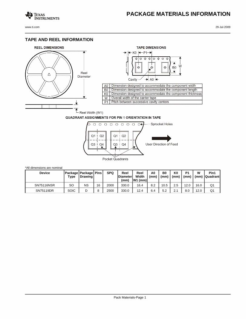
TAPE AND REEL INFORMATION
*All dimensions are nominal
Device PackageType
PackageDrawing
Pins SPQ ReelDiameter
(mm)
ReelWidth
W1 (mm)
A0(mm)
B0(mm)
K0(mm)
P1(mm)
W(mm)
Pin1Quadrant
SN75116NSR SO NS 16 2000 330.0 16.4 8.2 10.5 2.5 12.0 16.0 Q1
SN75119DR SOIC D 8 2500 330.0 12.4 6.4 5.2 2.1 8.0 12.0 Q1
PACKAGE MATERIALS INFORMATION
www.ti.com 29-Jul-2009
Pack Materials-Page 1

*All dimensions are nominal
Device Package Type Package Drawing Pins SPQ Length (mm) Width (mm) Height (mm)
SN75116NSR SO NS 16 2000 346.0 346.0 33.0
SN75119DR SOIC D 8 2500 340.5 338.1 20.6
PACKAGE MATERIALS INFORMATION
www.ti.com 29-Jul-2009
Pack Materials-Page 2


IMPORTANT NOTICE
Texas Instruments Incorporated and its subsidiaries (TI) reserve the right to make corrections, modifications, enhancements, improvements,and other changes to its products and services at any time and to discontinue any product or service without notice. Customers shouldobtain the latest relevant information before placing orders and should verify that such information is current and complete. All products aresold subject to TI’s terms and conditions of sale supplied at the time of order acknowledgment.
TI warrants performance of its hardware products to the specifications applicable at the time of sale in accordance with TI’s standardwarranty. Testing and other quality control techniques are used to the extent TI deems necessary to support this warranty. Except wheremandated by government requirements, testing of all parameters of each product is not necessarily performed.
TI assumes no liability for applications assistance or customer product design. Customers are responsible for their products andapplications using TI components. To minimize the risks associated with customer products and applications, customers should provideadequate design and operating safeguards.
TI does not warrant or represent that any license, either express or implied, is granted under any TI patent right, copyright, mask work right,or other TI intellectual property right relating to any combination, machine, or process in which TI products or services are used. Informationpublished by TI regarding third-party products or services does not constitute a license from TI to use such products or services or awarranty or endorsement thereof. Use of such information may require a license from a third party under the patents or other intellectualproperty of the third party, or a license from TI under the patents or other intellectual property of TI.
Reproduction of TI information in TI data books or data sheets is permissible only if reproduction is without alteration and is accompaniedby all associated warranties, conditions, limitations, and notices. Reproduction of this information with alteration is an unfair and deceptivebusiness practice. TI is not responsible or liable for such altered documentation. Information of third parties may be subject to additionalrestrictions.
Resale of TI products or services with statements different from or beyond the parameters stated by TI for that product or service voids allexpress and any implied warranties for the associated TI product or service and is an unfair and deceptive business practice. TI is notresponsible or liable for any such statements.
TI products are not authorized for use in safety-critical applications (such as life support) where a failure of the TI product would reasonablybe expected to cause severe personal injury or death, unless officers of the parties have executed an agreement specifically governingsuch use. Buyers represent that they have all necessary expertise in the safety and regulatory ramifications of their applications, andacknowledge and agree that they are solely responsible for all legal, regulatory and safety-related requirements concerning their productsand any use of TI products in such safety-critical applications, notwithstanding any applications-related information or support that may beprovided by TI. Further, Buyers must fully indemnify TI and its representatives against any damages arising out of the use of TI products insuch safety-critical applications.
TI products are neither designed nor intended for use in military/aerospace applications or environments unless the TI products arespecifically designated by TI as military-grade or "enhanced plastic." Only products designated by TI as military-grade meet militaryspecifications. Buyers acknowledge and agree that any such use of TI products which TI has not designated as military-grade is solely atthe Buyer's risk, and that they are solely responsible for compliance with all legal and regulatory requirements in connection with such use.
TI products are neither designed nor intended for use in automotive applications or environments unless the specific TI products aredesignated by TI as compliant with ISO/TS 16949 requirements. Buyers acknowledge and agree that, if they use any non-designatedproducts in automotive applications, TI will not be responsible for any failure to meet such requirements.
Following are URLs where you can obtain information on other Texas Instruments products and application solutions:
Products Applications
Audio www.ti.com/audio Communications and Telecom www.ti.com/communications
Amplifiers amplifier.ti.com Computers and Peripherals www.ti.com/computers
Data Converters dataconverter.ti.com Consumer Electronics www.ti.com/consumer-apps
DLP® Products www.dlp.com Energy and Lighting www.ti.com/energy
DSP dsp.ti.com Industrial www.ti.com/industrial
Clocks and Timers www.ti.com/clocks Medical www.ti.com/medical
Interface interface.ti.com Security www.ti.com/security
Logic logic.ti.com Space, Avionics and Defense www.ti.com/space-avionics-defense
Power Mgmt power.ti.com Transportation and Automotive www.ti.com/automotive
Microcontrollers microcontroller.ti.com Video and Imaging www.ti.com/video
RFID www.ti-rfid.com
OMAP Mobile Processors www.ti.com/omap
Wireless Connctivity www.ti.com/wirelessconnectivity
TI E2E Community Home Page e2e.ti.com
Mailing Address: Texas Instruments, Post Office Box 655303, Dallas, Texas 75265Copyright © 2011, Texas Instruments Incorporated