difference amplifier/common mode rejection ratio · pdf filedifference amplifier/common mode...
TRANSCRIPT

Difference Amplifier/Common Mode Rejection Ratio
Brad Peirson
4-7-2005
EGR 214 – Circuit Analysis I
Laboratory Section 04
Prof. Blauch
Abstract
The purpose of this laboratory is to determine the Common Mode Rejection Ratio
(CMRR) for a difference amplifier circuit. A difference amplifier is a circuit that will
amplify the difference between two input voltages. A circuit schematic was given, and
from this schematic the relationship between the input voltages and the output voltages
was determined. The circuit was then drawn in P-Spice and simulated. This same circuit
was then built using a u741 operational amplifier chip. The CMRR was determined
algebraically, from the P-Spice model and from the results of measurements using a
digital multi-meter. The simulated and experimental results were then compared against
the CMRR from the mathematical model. While not ideal, the simulated and
experimental common mode rejection ratios were extremely close to the mathematically
predicted CMRR. Because of this the circuit will likely not show any variation in output
due to electrical interference.
1.0 Introduction
The difference amplifier is a circuit that requires two separate input voltages. The
purpose of the circuit is to amplify the difference between two input voltages. The circuit
also has the capability to effectively ignore the inputs when they are the same. This
function is vital as all electronic circuits are exposed to interference. Often such
interference will result in the input signals having the same voltage value. An ideal
difference amplifier will reject all such interference and amplify only the difference
between the two inputs.
The key to the difference amplifier is an operational amplifier. Since its inception
nearly sixty years ago the operational amplifier has been a key component in computer
systems. The internal circuitry in the modern operational amplifier is a complex circuit
consisting of resistors, capacitors and inductors. This complex circuit can be considered
a black box, which greatly simplifies the analysis of any operational amplifier circuit.
Section 2 outlines the operation of the operational amplifier and the difference
amplifier circuit. It also details several properties of the difference amplifier circuit.
Section 3 is the analysis of the difference amplifier circuit using assigned nominal
resistance values. This section also contains the derivations of the inherent relationships
- 1 -

of the difference amplifier. Section 4 contains a P-Spice simulation of the difference
amplifier circuit. Section 5 analyzes the data gathered from the physical circuit. Section
6 is the results discussion section and section 7 is the conclusions section.
2.0 The Operational Amplifier
The Operational Amplifier (OP AMP) is a complex integrated circuit. OP AMPS
are amplifying circuits that were originally designed to perform mathematical operations.
Early OP AMP consisted of vacuum tubes in early analog computers. As technology
evolved, so too did the OP AMP. The most common OP AMP configuration in use today
is the 741 integrated circuit chip. Figure 1 shows the 741 chip pin diagram with an OP
AMP schematic diagram.
vN +VCC
vP vO
-VCC
Figure 1: u741 OP AMP Pin Diagram
The OP AMP itself is a five pin device. It is also an active device that depends on
present inputs as well as previous inputs to operate. This means that the device requires a
voltage to drive it. This voltage is +VCC and –VCC, the same voltage with the polarities
reversed. These voltages are shown on the pin diagram in Figure 1. Pins 4 and 7 are
typically left off of schematic diagrams for the sake of clarity, though the voltages are
assumed to be present. The output voltage of the OP AMP cannot exist outside the ±VCC
range. When the output voltage would be less than –VCC, the output stays at –VCC. This
is known as the –Saturation region. Likewise, the output voltage remains at +VCC when
it would be greater. This is known as the +Saturation regions. Between the saturation
regions the OP AMP is in the linear operation region. The output voltage of the OP AMP
in the linear region is determined by
- 2 -

( )NPO vvAv −= . (1)
The relationship of the three regions is shown in Figure 2.
Figure 2: OP AMP Characteristics
The slope of the graph in the linear region is the voltage gain, A, from (1). The range of
vO can be used to determine the two main characteristics of an ideal OP AMP. The
relationship of vO to ±VCC is
CCOCC VvV +≤≤− . (2)
When (1) is substituted into (2) the relationship between vP, vN and ±VCC is found to be
( )AV
vvAV CC
NPCC +
≤−≤−
. (3)
The voltage gain is typically very high in an OP AMP, usually on the order of 105. In an
ideal OP AMP the gain is assumed to be infinite. When this is the case, the relationship
in (3) becomes
( ) 00 ≤−≤ NP vv . (4)
This shows the first characteristic of an ideal OP AMP. The second characteristic of the
ideal OP AMP has to do with currents. The resistance across the two input terminals on
an ideal OP AMP is assumed to be infinite. By Ohm’s law this means that the current
entering both input nodes must be zero. So, the characteristics of an ideal OP AMP are
- 3 -

NP vv = (5)
and
0== NP ii . (6)
2.1 Difference Amplifier
The difference amplifier is a specific application of the OP AMP. This circuit
amplifies the difference between two separate input voltages and ignores common inputs.
The schematic for this type of circuit is shown in Figure 3.
1R 2R
3R
4R
1v
2v
_
+
+ v_
0
Figure 3: Difference Amplifier Circuit
The relationship of the inputs to the outputs of the difference amplifier can best be
described if two new voltages are defined. The differential mode voltage and the
common mode voltage (v
)( dmv
cm) are defined as
12 vvvdm −= (7)
and
2
21 vvvcm+
= . (8)
These new voltages relate to the output voltages linearly. The new relationship is
shown in (9).
dmdmcmcmO vAvAv += (9)
- 4 -

When the two input voltages are the same, they drive the differential mode term to zero.
This means that the common mode voltage only shows up in the equation when the two
inputs are the same voltage with the same polarity. In order to ensure that this voltage is
rejected the common mode gain must be zero. When this happens it can be shown that
dmcmO vRRvv
1
20 += . (10)
This relationship shows that any common mode voltage will be disregarded. Likewise
any differential mode voltage will be amplified by1
2
RR
.
The relationship in (10) holds true only for an ideal difference amplifier. In
practical application there are no ideal circuits, however. The common mode gain and
the differential mode gain can be used to determine the common mode rejection ratio
(CMRR). The CMRR is a measure of how close the circuit is to being ideal and is stated
mathematically as
cm
dm
AA
CMRR = . (11)
A high CMRR is the overall goal because a large CMRR means that the common mode
voltage will have almost no impact on the output voltage. This is necessary because of
the nature of the common mode voltage. When the two input voltages have the same
value this is typically a result of electrical “noise.” A high CMRR means that this
interference will have very effect on the operation of the circuit.
3.0 Analysis
The overall equation from the schematic in Figure 3 can be used to verify the
relationship in (9). This is done using the superposition principle. First, is suppressed
to find the output with respect to v
2v
1. The resulting superposition circuit is shown in
Figure 4.
R1 R2
- 5 -

iN
vN v1 _
++ vO1 _
vP
R3
R4
Figure 4: First Superposition Circuit
Figure 1 showed that the voltage entering the negative node of the OP AMP was denoted
as vN and the voltage entering the positive node was vP. There is no vP in this
superposition circuit so by the relationship in (5) vN = vP = 0. KCL at the negative OP
AMP node can be used to determine the vO relationship for this circuit.
02
1
1
1 =−−
+−
NONN i
Rvv
Rvv
(12)
When the properties of the ideal OP AMP from (5) and (6) are applied to (12) the
relationship for the first output voltage can be found. This derivation is shown in (13),
(14) and (15).
02
1
1
1 =+Rv
Rv O (13)
1
1
2
1
Rv
RvO −= (14)
11
21 v
RRvO −= (15)
Once the relationship for vO1 is derived, the second superposition circuit can be
solved. This circuit is shown in Figure 5 below.
R1 R2
- 6 -

vN _
+vP +
vO2 _
R3
v2
R4
Figure 5: Second Superposition Circuit
By observing Figure 5 it can be seen that vN and vP can be found using voltage dividers.
These equations are
221
1ON v
RRRv+
= (16)
and
243
4 vRR
RvP += . (17)
Because OP AMPs have the property that vP = vN , (16) and (17) can be set equal to one
another and solved to find the relationship for the second output voltage. This full
derivation is shown in (18) through (21).
243
42
21
1 vRR
RvRR
RO +
=+
(18)
2431
2142 )(
)( vRRRRRRvO +
+= (19)
2
4
341
2
142
2
1
1v
RRRR
RRRR
vO
⎟⎠⎞⎜
⎝⎛ +
⎟⎠⎞⎜
⎝⎛ +
= (20)
2
4
31
2
12
2
1
1v
RRR
RRR
vO
⎟⎠⎞⎜
⎝⎛ +
⎟⎠⎞⎜
⎝⎛ +
= (21)
- 7 -

The final relationship for vO is the sum of the superposition solutions, and is
stated as
11
22
4
31
2
12
1
1v
RR
v
RRR
RRR
vO −⎟⎠⎞⎜
⎝⎛ +
⎟⎠⎞⎜
⎝⎛ +
= . (22)
At this point the relationship is in terms of the original input voltages. As shown
in section 2.1, the input voltages can be restated in terms of the common and differential
mode voltages. From (7) and (8) the values of the input voltages in terms of the mode
voltages were determined. These values are
dmcm vvv21
1 −= (23)
and
dmcm vvv21
2 += . (24)
These values can be substituted into (22) to determine the relationship between vP, vN and
vO. The complete derivation of this new relationship is shown below.
⎟⎠⎞
⎜⎝⎛ −−⎟
⎠⎞
⎜⎝⎛ +⎟⎟⎟⎟
⎠
⎞
⎜⎜⎜⎜
⎝
⎛
+
+= dmcmdmcmO vv
RRvv
RR
RR
RRv
21
21
1
1
1
2
4
3
2
1
1
2 (25)
1
2
4
311
12
1
2
4
311
12
22 RvR
RRRR
vRvRRvR
RRRR
vRvRv dmdmdmcmcmcm
O +⎟⎠⎞⎜
⎝⎛ +
++−
+
+= (26)
dmcmO vR
R
RRRR
RRv
RR
RRRR
RRv
⎟⎟⎟⎟
⎠
⎞
⎜⎜⎜⎜
⎝
⎛
+⎟⎠⎞⎜
⎝⎛ +
++
⎟⎟⎟⎟
⎠
⎞
⎜⎜⎜⎜
⎝
⎛
−+
+=
1
2
4
311
12
1
2
4
311
12
22 (27)
( ) dmcmO v
RRRRR
RRRRRR
v
RRRRR
RRRRRR
v⎟⎟⎟⎟
⎠
⎞
⎜⎜⎜⎜
⎝
⎛
+
++++
⎟⎟⎟⎟
⎠
⎞
⎜⎜⎜⎜
⎝
⎛
+
−−+=
4
3141
4
32212
4
3141
4
32212
2 (28)
dmcmO vRRRR
RRRRRRRRv
RRRRRRRR
v ⎟⎟⎠
⎞⎜⎜⎝
⎛+
++++⎟⎟
⎠
⎞⎜⎜⎝
⎛+−
=3141
32424142
3141
3241
22 (29)
- 8 -
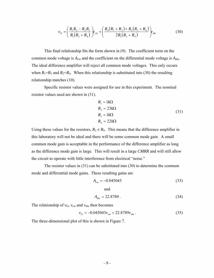
( )( ) ( )
( ) dmcmO vRRR
RRRRRRv
RRRRRRR
v ⎟⎟⎠
⎞⎜⎜⎝
⎛+
++++⎟⎟
⎠
⎞⎜⎜⎝
⎛+−
=431
432214
431
3241
2 (30)
This final relationship fits the form shown in (9). The coefficient term on the
common mode voltage is Acm and the coefficient on the differential mode voltage is Adm.
The ideal difference amplifier will reject all common mode voltages. This only occurs
when R1=R3 and R2=R4. When this relationship is substituted into (30) the resulting
relationship matches (10).
Specific resistor values were assigned for use in this experiment. The nominal
resistor values used are shown in (31).
Ω=Ω=Ω=
Ω=
kRkR
kRkR
221231
4
3
2
1
(31)
Using these values for the resistors, R2 ≠ R4. This means that the difference amplifier in
this laboratory will not be ideal and there will be some common mode gain. A small
common mode gain is acceptable in the performance of the difference amplifier as long
as the difference mode gain is large. This will result in a large CMRR and will still allow
the circuit to operate with little interference from electrical “noise.”
The resistor values in (31) can be substituted into (30) to determine the common
mode and differential mode gains. These resulting gains are
045043.0−=cmA (33)
and
8789.22=dmA . (34)
The relationship of vO, vcm and vdm then becomes
dmcmO vvv 8789.22045043.0 +−= . (35)
The three-dimensional plot of this is shown in Figure 7.
- 9 -

Figure 7: 3-D Plot of vO using analysis data
Figure 7 shows that while (35) is not ideal, there is very little change due to vcm meaning
the impact it has on the equation is negligible. The CMRR for this model is
93464.507045043.08789.22
=−
=CMRR . (36)
Because this CMRR only involves nominal resistor values (36) will be the standard
against which the simulated and experimental results will be checked.
4.0 Simulation
The resistor values in (31) were input into P-Spice. There were two separate sets
of simulations run: one set where v1 = v2 and one set where v1 = -v2. For the first set the
vdm term in (9) became zero. For the second set the vcm term in (9) became zero. An
example of the P-Spice results for one of the simulations is shown in Figure 8.
- 10 -

Figure 8: P-Spice Simulation Schematic (v1 = v2 = 2V)
The results of the P-Spice simulations for v1 = v2 are given in Table 1. The common and
differential mode voltages were found by substituting the values of v1 and v2 into (7) and
(8). The common mode gain was calculated by substituting the values for vcm, vdm and vO
into (9).
- 11 -

Table 1: Common Mode Gain Simulation Results
v1 (V) v2 (V) vcm vdm vO (mV) Acm1 1 1 0 -47.73 -0.04773 2 2 2 0 -87.93 -0.043965 3 3 3 0 -132.12 -0.04404 4 4 4 0 -176.31 -0.044078 5 5 5 0 -220.49 -0.044098 6 6 6 0 -264.67 -0.044112
The data in Table 1 was input into a Microsoft Excel spreadsheet. The common mode
voltage was then plotted against vO and a linear regression was performed. This plot is
given in Figure 9.
y = -0.0436x - 0.0022R2 = 0.9998
-0.3
-0.25
-0.2
-0.15
-0.1
-0.05
00 1 2 3 4 5 6 7Vcm
Vo
Figure 9: vcm vs. vO for the simulated common mode gain
The common mode gain is the slope of the vcm vs. vO trend line. Figure 8 shows
that the common mode gain for the simulated results was -0.0436. This was the common
mode gain used in determining the relationship of vO to the common mode and
differential mode voltages.
After the simulations to determine the common mode gain, the simulations for the
differential mode gain were run. Again the values for vcm, vdm and vO were substituted
into (9) to determine the gain. The simulation results are shown in Table 2.
- 12 -

Table 2: Differential Mode Gain Simulation Results
v1 (V) v2 (V) vcm vdm vO (V) Adm-0.01 0.01 0 0.02 0.45997 22.9985 -0.02 0.02 0 0.04 0.91947 22.9868 -0.03 0.03 0 0.06 1.379 22.9833 -0.04 0.04 0 0.08 1.839 22.9875 -0.05 0.05 0 0.10 2.298 22.98 -0.06 0.06 0 0.12 2.758 22.9833
This data was again input into an Excel spreadsheet. The resulting plot with trend line is
given in Figure 10.
y = 22.98x + 0.0003R2 = 1
0
0.5
1
1.5
2
2.5
3
0 0.02 0.04 0.06 0.08 0.1 0.12 0.14
Vdm
Vo
Figure 10: vdm vs. vO for the simulated differential mode gain
Again, the slope of the plot shown in figure t is the differential mode gain. Both
of the gains determined in the regressions were input into (9) in order to determine the
relationship for the simulation data. This relationship was found to be
dmcmO vvv 98.220436.0 +−= . (37)
This equation was then graphed on a three dimensional coordinate system. The resulting
graph is shown in Figure 11.
- 13 -

Figure 11: 3-D Plot of vO using simulated data
The CMRR for the simulation data was
064.5270436.098.22
=−
=CMRR . (38)
5.0 Experimental Results
Four resistors with nominal values shown in (31) were chosen. The actual
resistances were measured and recorded in Table 3.
Table 3: Resistor Values
Resistor Nominal Value (kΩ) Measured Value (kΩ) R1 1 0.994 R2 23 22.764 R3 1 0.994 R4 22 21.74
The circuit in Figure 3 was built on the CADET circuit trainer using the resistors in Table
3. The first set of data measured was used to determine Acm. To do this the input
voltages were equal to one another. This makes the differential mode voltage zero. The
values were then substituted into (9) and solved for Acm. The results of these
measurements and calculations are given in Table 4.
- 14 -

Table 4: Common Mode Gain Experimental Results
v1 (V) v2 (V) vcm vdm vO (mV) Acm1.01 1.01 1.01 0 -0.038 -0.037624 2.00 2.00 2.00 0 -0.077 -0.0385 3.057 3.057 3.057 0 -0.101 -0.033039 4.08 4.08 4.08 0 -0.138 -0.033824 5.03 5.03 5.03 0 -0.179 -0.035586 6.08 6.08 6.08 0 -0.215 -0.035362
The experimental data was then input into an Excel spreadsheet. A regression
analysis was performed. The resulting plot is shown in Figure 12.
y = -0.0346x - 0.0021R2 = 0.9943
-0.25
-0.2
-0.15
-0.1
-0.05
00 1 2 3 4 5 6 7Vcm
Vo
Figure 12: vcm vs. vO for the experimental common mode gain
Again, the common mode gain will be the slope of the trend line in Figure 12.
The common mode gain for this experiment was -0.0346. The same type of process was
used for the differential mode data in Table 5.
- 15 -

Table 5: Differential Mode Gain Experimental Results
v1 (V) v2 (V) vcm vdm vO (V) Adm4.98 5 4.99 0.02 0.942 55.733 4.80 5 4.9 0.2 4.97 25.698 4.68 5 4.84 0.32 7.47 23.867 4.47 5 4.735 0.53 11.32 21.668 4.28 5 4.64 0.72 11.32 15.945 4.84 5 4.92 0.16 3.91 25.501
In this experiment, it was impractical to use equal but opposite voltages for v1 and
v2. There were two difficulties with the original set-up. First, if a single power supply
was used to provide the opposite voltages the supply would be shorted. This had the
potential of damaging the power supply. The second difficulty came if two supplies were
used to provide the opposite voltages. This meant that the power supplies would have
had to have been moved from one lab station to another. This method would have been
impractical. It was determined that since there was no practical way to provide the
necessary equal and opposite voltages, the voltages would be chosen sufficiently close to
one another so that the common mode voltage would be nearly constant. The gain could
be calculated using the common mode gain, the common mode voltage and the
differential mode voltage as in the previous data set. The data in Table 5 was again input
into Excel and a linear regression was performed. This regression plot is shown in Figure
13.
- 16 -

y = 15.574x + 1.5938R2 = 0.9289
0
2
4
6
8
10
12
14
0 0.1 0.2 0.3 0.4 0.5 0.6 0.7 0.8
Vdm
Vo
Figure 13: vcm vs. vO for the experimental differential mode gain
The R2 value of the regression line in Figure 13 seemed too low for an accurate
best-fit line. The data was checked, and it was determined that the circuit was saturating
when the difference mode voltage was approximately 0.5. This was found to be the two
data points that resulted in vO=11.32. These two data points were left out of the
regression model, resulting in Figure 14.
- 17 -

y = 21.846x + 0.4999R2 = 0.9992
012345678
0 0.05 0.1 0.15 0.2 0.25 0.3 0.35
Vdm
Vo
Figure 14: Modified vdm regression plot
The R2 value in Figure 14 was much higher than that in Figure 13 meaning that the
regression line is a better fit. The model in Figure 14 was the Adm value used for the vO
equation. The experimental vO equation was
dmcmO vvv 846.210346.0 +−= . (39)
This equation was then used in generating the three dimensional graph of vO. This graph
is given in Figure 15.
Figure 15: 3-D Plot of vO using experimental data
- 18 -

Finally, the CMRR for the experimental data was calculated in (40).
387.6310346.0846.21
=−
=CMRR (40)
6.0 Discussion
The CMRR based solely on the nominal resistance values in the circuit was
approximately 507. The CMRR calculated in section 4 was approximately 527, and the
CMRR from the experimental data was approximately 631. These values were all large
enough to conclude that outside electrical interference will not have any effect on the
operation of the circuit.
This is supported by the 3-D graphs in each section. Each of these plots showed
very little change due to the x-variable, vcm. This suggests that in each of the equations,
the common mode gain was nearly zero. In fact, when arbitrary values were chosen for
vcm and vdm it required an increase of nearly 1000 volts in vcm to create a noticeable
difference in vO.
The only discrepancy in the results of each model is in the CMRR for the
experimental data. This value was greater than the other two by approximately 100.
There were two possible explanations for this difference. The main reason was the
resistor values. The analysis and simulation CMRRs assumed that the resistances were all
equal to the nominal value. For the experimental CMRR, the resistances varied within the
allowable ±5% tolerance rating. This variance was likely large enough to cause a good
portion of the difference. The second reason for the difference between CMRRs was the
method in which the experimental vdm data was collected. In the ideal model, the
common mode gain is zero. In turn, since the common mode gain in the experimental
calculations was known to be non-zero the common mode voltage would have had to
have been zero. This proved impractical in the lab. Instead it was proposed that if v1 and
v2 were kept close enough together the common mode voltage could be assumed to be
constant. This assumption is the second source of error. The common mode voltage was
nearly constant but there was some amount of variation.
- 19 -

7.0 Conclusions
The difference amplifier circuit is a circuit that amplifies the difference between
two input signals. A mathematical model for the relationship of the output voltage to the
input voltage was derived in section 3.0. This model was used as the standard against
which the simulated and experimental results were checked. Because of the overall
precision in the three different common mode rejection ratios the results of the
experiment verify the characteristics of the ideal difference amplifier, also discussed in
section 3.0. In addition, the CMRR for all three sections was high enough to be
reasonably certain that electrical “noise” will not have any noticeable effect on the output
of the difference amplifier circuit.
- 20 -