devicenet scanner module - yokogawa · pdf fileinstruction manual yokogawa electric...
TRANSCRIPT

InstructionManual
Yokogawa Electric Corporation
IM 34M6H28-01E
DeviceNet Scanner Module
IM 34M6H28-01E1st Edition

<Toc> <Ind> <Rev> <Preface> i
IM 34M6H28-01E
Applicable Product:FA-M3 Range-free Multi-Controller
Model: F3LD01-0N
Name: DeviceNet Scanner Module
The document number and document model code for this manual are as follows:
Document No.: IM 34M6H28-01E
Document Model Code: DOCIM
Refer to the document number in all communications; also refer to the document
number or the document model code when purchasing additional manuals.
1st Edition : Feb.01,1999-00Media No. IM 34M6H28-01E (CD) 1st Edition : Feb. 1999 (YK)All Rights Reserved Copyright © 1999, Yokogawa Electric Corporation

ii<Toc> <Ind> <Rev> <Preface>
IM 34M6H28-01E 1st Edition : Feb.01,1999-00
Important
About This Manual(1) This manual should be passed on to the end user.
(2) Before using the module, read this manual completely to get a thorough understand-ing of the module.
(3) This manual explains the functions contained in this product, but does not warrant thatthose will suit the particular purpose of the user.
(4) Under absolutely no circumstances may the contents of this manual be transcribed orcopied, in part or in whole, without permission.
(5) The contents of this manual are subject to change without prior notice.
(6) Every effort has been made to ensure accuracy in the preparation of this manual.However, should any errors or omissions come to the attention of the user, pleasecontact the nearest Yokogawa Electric representative or sales office.

<Toc> <Ind> <Rev> <Preface> iii
IM 34M6H28-01E 1st Edition : Feb.01,1999-00
Safety Precautions when Using/Maintaining the ProductThe following safety symbols are used on the product as well as in this manual.
CAUTIONThis symbol indicates that the operator must follow the instructions laid out in thismanual in order to avoid the risk of personnel injuries or fatalities or damage to theinstrument. The manual describes what special care the operator must exercise toprevent electrical shock or other dangers that may result in injury or the loss of life.
Protective ground terminal
Before using the instrument, be sure to ground this terminal.
Function ground terminal
Before using the instrument, be sure to ground this terminal.
Indicates alternating current.
Indicates direct current.
(1) The following symbols are used only in the instruction manual.
WARNINGIndicates that the operator must refer to the instructions in this manual in order toprevent the instrument (hardware) or software from being damaged, or a systemfailure from occurring.
CAUTIONDraws attention to information essential for understanding the operation and functions.
TIP
Gives information that complements the present topic.
SEE ALSO
Identifies a source to which to refer.
(2) For the protection and safe use of the product and the system controlled by it, be sureto follow the instructions and precautions on safety stated in this manual wheneverhandling the product. Take special note that if you handle the product in a mannerother than prescribed in these instructions, safety cannot be guaranteed.
(3) If separate protection and/or safety circuits for this product or the system which iscontrolled by this product are to be installed, ensure that such circuits are installedexternal to the product.
(4) If component parts or consumables are to be replaced, be sure to use parts specifiedby the company.

iv<Toc> <Ind> <Rev> <Preface>
IM 34M6H28-01E 1st Edition : Feb.01,1999-00
(5) Do not attempt to make modifications or additions internal to the product.
Force Majeure(1) Yokogawa Electric Corporation (hereinafter referred to as Yokogawa Electric) makes
no warranties regarding the product except those stated in the WARRANTY that isprovided separately.
(2) Yokogawa Electric assumes no liability to any party for any loss or damage, direct orindirect, caused by the user or any unpredictable defect of the product.
Software Supplied by the Company(1) Yokogawa Electric makes no other warranties expressed or implied except as pro-
vided in its warranty clause for software supplied by the company.
(2) Use the relevant software with one specified computer only. You must purchaseanother copy of the software for use with each additional computer.
(3) Copying the software for any purpose other than backup is strictly prohibited.
(4) Store the floppy disks (originals) of this software in a safe place.
(5) Reverse engineering, such as decompiling of the software, is strictly prohibited.
(6) No portion of the software supplied by Yokogawa Electric may be transferred, ex-changed, or sublet or leased for use by any third party without prior permission byYokogawa Electric.

<Toc> <Ind> <Rev> <Preface> v
IM 34M6H28-01E 1st Edition : Feb.01,1999-00
General Requirements for Using FA-M3 Controllers
Avoid installing FA-M3 controllers in the following locations:
• Where the instrument will be exposed to direct sunlight, or where the operating tem-perature is outside the range 08 to 558C.
• Where the relative humidity is outside the range 10 to 90%, or where sudden tempera-ture changes may occur and cause condensation.
• Where corrosive or inflammable gases are present.
• Where the instrument will be exposed to direct mechanical vibration or shock.
Securely tighten screws:
• Securely tighten module mounting screws and terminal screws to avoid problemssuch as faulty operation.
Securely fasten connectors of interconnecting cables:
• Securely fasten connectors of interconnecting cables, and check them thoroughlybefore turning on the power.
Interlock with emergency-stop circuitry using external relays:
• Equipment incorporating the FA-M3 controllers must be furnished with emergency-stop circuitry that uses external relays. This circuitry should be set up to interlockcorrectly with controller status (stop/run).
Ground FA-M3 controllers to an independent Japanese Industrial Standard(JIS) Class 3 Ground:
• Avoid grounding the FG terminal of the FA-M3 controller to the same ground as high-voltage power lines. Ground the terminal to an independent JIS Class 3 ground(ground resistance up to 100 Ω).
Observe countermeasures against noise:
• When assigning inputs/outputs, the user should avoid locating AC-supplied I/O mod-ules in the vicinity of the CPU module.
Keep spare parts on hand:
• Stock up on maintenance parts, including spare modules, in advance.
Discharge static electricity before operating the system:
• Because static charge can accumulate in dry conditions, first touch grounded metal todischarge any static electricity before touching the system.
Never use solvents such as paint thinner for cleaning:
• Gently clean the surfaces of the FA-M3 controllers with a piece of soft cloth soaked inwater or a neutral detergent.
• Do not use solvents such as paint thinner for cleaning, as they may cause deforma-tion, discoloration, or malfunctioning.

vi<Toc> <Ind> <Rev> <Preface>
IM 34M6H28-01E 1st Edition : Feb.01,1999-00
Avoid storing the FA-M3 controllers in places with high temperature orhumidity:
• Since the CPU module has a built-in battery, avoid storing it in places with high tem-perature or humidity.
• Since the service life of the battery is drastically reduced by exposure to high tem-peratures, so take special care (storage temperature can be from -208 to 758C).
Always turn off the power before installing or removing modules:
• Turn off power to the power supply module when installing or removing modules,otherwise damage may result.
When installing ROM packs and changing switch settings:
• In some modules you can remove the right-side cover and install ROM packs orchange switch settings. While doing this, do not touch any components on the printed-circuit board, otherwise components may be damaged and modules fail.

<Toc> <Ind> <Rev> <Preface> vii
IM 34M6H28-01E
Waste Electrical and Electronic EquipmentWaste Electrical and Electronic Equipment (WEEE), Directive 2002/96/EC(This directive is only valid in the EU.)
This product complies with the WEEE Directive (2002/96/EC) marking requirement.
The following marking indicates that you must not discard this electrical/electronic productin domestic household waste.
Product Category
With reference to the equipment types in the WEEE directive Annex 1, this product isclassified as a “Monitoring and Control instrumentation” product.
Do not dispose in domestic household waste.
When disposing products in the EU, contact your local Yokogawa Europe B. V. office.
1st Edition : Feb.01,1999-00

viii<Toc> <Ind> <Rev> <Preface>
IM 34M6H28-01E 1st Edition : Feb.01,1999-00
Introduction
Overview of the ManualThis is the instruction manual of the DeviceNet Scanner Module of the FA-M3 Multi-control-ler.
Other Instruction ManualsConsult the following FA-M3 manuals as necessary when using this module:
• Sequence CPU Instruction Manual – Functions (IM 34M6P12-02E)
• Sequence CPU Instruction Manual – Instructions (IM 34M6P12-03E)
• Sequence CPU Instruction Manual (for F3FP36) (IM 34M6P22-01E)
• Personal Computer Link Command Module Instruction Manual (IM 34M6P41-01E)
• Ladder Diagram Support Program M3 Instruction Manual (IM 34M6Q13-01E)
• BASIC CPU Module and BASIC Programming Tool M3 Instruction Manual (IM34M6Q22-01E)
Copyright/Trademarks• DeviceNet is a registered trademark of ODVA (Open DeviceNet Vendor Association,
Inc.).
• COMBICON is a registered trademark of Phoenix Contact Co., Ltd.
• All the product names and company names mentioned in this manual are the trade-marks or registered trademarks of their respective companies.
• The copyright of the software loaded in this module belongs to SST Inc. (S-S Tech-nologies).
Terminology Used• This manual uses terminology in the DeviceNet Specification published by ODVA.

Toc-1<Int> <Ind> <Rev>
IM 34M6H28-01E
CONTENTS
1st Edition : Feb.01,1999-00
FA-M3DeviceNet Scanner Module
IM 34M6H28-01E 1st Edition
Important ...................................................................................................... ii
Introduction................................................................................................ viii
1. Overview .................................................................................................. 1-1
2. Overview of DeviceNet.............................................................................. 2-12.1 Network Configuration....................................................................................... 2-1
2.2 I/O Communications (I/O Slave Message) ......................................................... 2-3
2.3 Message Communications (Explicit Peer-to-Peer Message) ............................. 2-4
3. Preparations for Operation ........................................................................ 3-1
4. Module Specifications ............................................................................... 4-14.1 Function Specifications ..................................................................................... 4-1
4.2 Operating Environment ..................................................................................... 4-3
4.3 Model and Suffix Codes .................................................................................... 4-3
4.4 Components ..................................................................................................... 4-3
4.5 Display Panel .................................................................................................... 4-4
4.6 Setting Switches ............................................................................................... 4-5
4.6.1 Node Address Setting Switch............................................................ 4-5
4.6.2 Operation Mode Setting Switch ......................................................... 4-5
4.6.3 Terminating Resistor Setting Switch .................................................. 4-6
4.7 External Dimensions ......................................................................................... 4-7
5. Attaching and Wiring ................................................................................. 5-15.1 Attaching and Detaching a Module .................................................................... 5-1
5.2 External Wiring.................................................................................................. 5-3
6. Module Access ......................................................................................... 6-16.1 I/O Relay ........................................................................................................... 6-1
6.2 I/O Data Register .............................................................................................. 6-2
6.3 Access from the CPU Module ........................................................................... 6-4
6.3.1 Access Using Ladder Sequence ....................................................... 6-4
6.3.2 Access Using BASIC ........................................................................ 6-5
7. I/O Communications ................................................................................. 7-17.1 Scan List ........................................................................................................... 7-1
7.2 Module Operation ............................................................................................. 7-4
7.3 Transmission Time Intervals ............................................................................ 7-10
7.4 I/O Response Time ......................................................................................... 7-11

<Int> <Ind> <Rev>
IM 34M6H28-01E
Toc-2
1st Edition : Feb.01,1999-00
7.5 Start/Stop Operation and Status Management(Example of Programming) ............................................................................. 7-12
7.6 I/O Data Access (Example of Programming) ................................................... 7-16
8. Message Communications........................................................................ 8-18.1 Module Operation ............................................................................................. 8-1
8.2 Interface ............................................................................................................ 8-4
8.2.1 Request and Response Formats ...................................................... 8-4
8.2.2 Exit Codes ........................................................................................ 8-5
8.3 Sample Programs ............................................................................................. 8-6
9. Configuration ............................................................................................ 9-1
9.1 Tool Commands ................................................................................................ 9-1
9.1.1 Commands ....................................................................................... 9-1
9.1.2 Request Procedure ........................................................................... 9-2
9.1.3 Basic Command Formats ................................................................. 9-4
9.1.4 Details of Commands ....................................................................... 9-5
9.1.5 Exit Codes ...................................................................................... 9-10
9.2 Configuration Procedure ..................................................................................9-11
9.3 Sample Program ............................................................................................. 9-12
10. Errors and Troubleshooting ..................................................................... 10-1
10.1 Flowchart When RDY LED Is Not ON.............................................................. 10-2
10.2 Flowchart When MS LED Is Flashing .............................................................. 10-3
10.3 Flowchart When NS LED Is Not ON ................................................................ 10-4
10.4 Flowchart When Red NS LED Is ON ............................................................... 10-5
10.5 Flowchart When Red NS LED Is Flashing ....................................................... 10-6
10.6 Error Codes .................................................................................................... 10-7
11. DeviceNet Glossary .................................................................................11-1
Appendix 1. Details on Network Configuration........................................ Appx.1-1Appendix 1.1 Cable Length .................................................................................. Appx.1-1
Appendix 1.2 Connection Methods ...................................................................... Appx.1-3
Appendix 1.3 Terminating Resistor ....................................................................... Appx.1-5
Appendix 1.4 Configuration of Network Power Supply ......................................... Appx.1-6
Appendix 1.5 Network Grounding ...................................................................... Appx.1-10
Appendix 2. Information on Third-party Products .................................... Appx.2-1
Revision History ....................................................................................................... i

<Toc> <Ind> <1. Overview > 1-1
IM 34M6H28-01E 1st Edition : Feb.01,1999-00
1. OverviewThe F3LD01-0N DeviceNet Scanner Module (hereafter referred to as this module) is a
module for connecting to DeviceNet.
What is a DeviceNet?DeviceNet is an open field network and is mainly used in manufacturing equipment or inproduction lines. In a multi-vendor environment, a wide range of devices, ranging fromsensors and actuators to advanced equipment which is compatible with DeviceNet, can beconnected.
As the specifications of DeviceNet are open and licensing is not required, many manufac-turers, both in Japan and overseas, are developing new devices which, when connectedwith DeviceNet, allow exchanges of I/O data. Overseas service has also become possible.Further, many types of I/O communications and message communications are supported.Decentralized control with multi-master systems is also possible now.
A maximum of 64 machines (masters + slaves) can be connected to DeviceNet. Themaximum data rate is 500 kbps and the maximum trunk line distance is 500 m (when thedata rate is 125 kbps). Thus, with these special characteristics of high connectability tomany stations, a high data rate and a long distance, DeviceNet can be used in a wide rangeof applications. Wiring can be done effectively by freely combining the T-branching methodand daisy chain method, with no wastage.
Each equipment type is defined by a device profile (specifications which define the opera-tion of the equipment). Equipment is built according to these profiles, thus resulting in thecompatibility and interchangeability of the equipment.
Personal computer/Workstation
FA-M3Special
purpose controller
etc
Display
Remote I/O Information device
Analog terminal
All types of sensors/actuators
Gateway to other networks
Higher-level network
DeviceNet
. Valve
. Solenoid
. Signal convertor
. Inverter
. Barcode reader
. ID System. All types of sensor paths. RS-232-C
F0101.EPS
T branching
Drop-line branching
Daisy chain
FA-M3
* : Mass flow controller, temperature control and monitoring guage, robot controller, etc.
Figure 1.1 Example of a DeviceNet Connection

1-2<Toc> <Ind> <1. Overview >
IM 34M6H28-01E 1st Edition : Feb.01,1999-00
Features of this moduleThis module has the master functions of DeviceNet. Using this module, you can exchangeI/O data periodically with other connected devices and exchange message data like param-eters and status.
The following are the main features of this module.
• A maximum of 63 slave machines can be connected.
• Data rate is 125/250/500 kbps.
• Supports an I/O communication function which regulates and controls I/O data of16,000 points (input 8,000 points; output 8,000 points). Anything from small-scale I/Odata to multiple-point analog data and information data can be handled in real time.
• A message communication function is supported. If required, the exchange of mes-sage data like parameters and status is also possible. Therefore, the time required forsystem configuration is reduced, and maintenance as well as calibration becomeseasier.
• Operation in a multi-master environment with decentralized control is also possible.
• 16 modules of this kind can be installed in a single FA-M3. It is easy to manage mul-tiple-point I/O data and to add new lines.
• The transmission time interval of I/O data can be set for every 5 msec. Thus, it iscompatible even with a slow-responding slave.

<Toc> <Ind> <2. Overview of DeviceNet > 2-1
IM 34M6H28-01E 1st Edition : Feb.01,1999-00
2. Overview of DeviceNetAn explanation of the functions which are supported by this module and which are relatedto the DeviceNet specifications is given here.
SEE ALSO
1) For details on the DeviceNet specifications, see also to the DeviceNet Specifications Manual, publishedby ODVA (Open Device Net Vendor Association, Inc.). ODVA is a non-profit company, formed by vendorswith the objective to promote and manage the DeviceNet specifications.
2) For product information of third-party products required for network configuration, refer to Appendix 2,“Information on Third-party Products.”
2.1 Network ConfigurationThe network configuration of DeviceNet is given below.
Node Node Node
Node
NodeNode Node
Tap
Tap
Power supply Tap
Network power supply
Terminating resistor
Node Node NodeMultiple-nodedaisy chain
T-branching
Drop-line branchingTrunk lineDrop line F0201.EPS
Tap Tap Tap Terminating resistor
Figure 2.1 Network Media Topology
The elements of the network configuration are explained below.
• Node
A device (equipment) that is connected to DeviceNet is called a node. A node can be eithera master, which collects and distributes data, or a slave, which outputs and inputs dataaccording to the instructions received from the master.
There are no restrictions on the arrangements or maximum number of devices that can beconnected to the master of each of the slaves. A maximum of 64 devices can be freelyconnected (without arrangement restrictions).
An address from 0 to 63, called MACID (Media Access Control Identifier), is assigned toeach node. In this manual, these addresses are called node addresses.

2-2<Toc> <Ind> <2. Overview of DeviceNet >
IM 34M6H28-01E 1st Edition : Feb.01,1999-00
• Cable
Five special purpose cables (2 signal lines, 2 power supply lines, and 1 SHIELD cable) areused. There are 2 types of cables, namely, thick cables and thin cables .
• Trunk Line
Terminating resistors are attached at both ends of this cable. Both thick and thin cables canbe used. They can also be used together.
For a thin cable, the maximum network length is 100 m. In the case of thick cables, thelength limits depends on the data rate (see Table 2.1).
• Drop line
This is a branch cable from the trunk line and normally, thin cables are used for this pur-pose.
The length (the distance from the point of branching from the trunk line to the end of thedrop line) of a drop-line cable should be 6 m or less. (There are no minimum distancelimits.) Generally, the total drop-line length depends on the data rate (see Table 2.1).
Table 2.1 Maximum Cable Length of DeviceNet
Data rateMaximum cable length of trunk line Length of drop line
Only thick cables usedOnly thin cable
usedMaximum Cumulative
125 kbps 500 m
100 m 6 m
156 m
250 kbps 250 m 78 m
500 kbps 100 m 39 mT0201.EPS
• Connection Method
There are 2 methods of wire connection, the T-branching (using the T-branching tap) andmultiple-node daisy-chain methods. In a trunk line/ drop line, both methods can be com-bined.
• Terminating Resistor
Terminating resistors (121V) are attached to both ends of a trunk line. This reduces thereflection of signals and stabilizes communication.
In this module, there is a built-in terminating resistor. Therefore, when connecting the trunkline using the daisychain method, you can turn on the terminating resistor setting switchand use the built-in terminating resistor. In other connection methods, please turn theswitch off so that the built-in terminating resistor is not used.
• Network Power Supply
Out of the 5 special-purpose cables, two are for the 24 V DC network power supply. It isnecessary to supply power to each node of the network using the cables. If a single net-work power supply source is used in a network, you can connect the power supply directlyto the trunk line. However, if multiple power supply sources are to be used in the network, itis necessary to use special-purpose power supply taps.

<Toc> <Ind> <2. Overview of DeviceNet > 2-3
IM 34M6H28-01E 1st Edition : Feb.01,1999-00
2.2 I/O Communications (I/O Slave Message)This is a communication function which allows the exchange of control information (I/Odata) between the master and a slave in real time.
This module supports the following two types of I/O communications protocols ofDeviceNet.
Polling.......... Sends polling instructions containing output data from the master to aspecified slave; the master then receives a response containing the inputdata from the slave
(1 : 1 communication).
Bit Strobe..... Multicasts (broadcasts) Bit Strobe request instructions from the master tomultiple slave systems and receives a response with input data from eachslave. A communication request that can be transmitted to multiple slavesat a time (1:N communications) will improve network throughput. However,this is possible only in the case of slave systems with input data of less than8 bytes.
In this module, transmission of I/O communications requests is cyclic. This period (trans-mission time interval) can be specified for all the slaves in a batch in 5 ms intervals.
Cyclic Request
Bit Strobe request instructions
Request/response with data
Response without data
This module (Master)
Input data Input data Output data Input/Output data
DeviceNet
F0202.EPS
Slave Slave Slave Slave
Figure 2.2 I/O Communications Concept Diagram
SEE ALSO
For information on I/O communications functions other than Polling and Bit Strobe, see also the“DeviceNet Specification” published by ODVA.

2-4<Toc> <Ind> <2. Overview of DeviceNet >
IM 34M6H28-01E 1st Edition : Feb.01,1999-00
2.3 Message Communications (Explicit Peer-to-Peer Message)This is a function for setting and reading parameters, controlling and managing operationsand exchanging information between nodes (1: 1) when necessary. In this module, it ispossible to send a service request to other nodes (master and slaves) using the explicitmessages defined in DeviceNet.
RequestRequest
Response
Response
F0203.EPS
Slave Slave
FA-M3
DeviceNet
Other masters
Slave
Figure 2.3 Message Communications Concept Diagram

<Toc> <Ind> <3. Preparations for Operation > 3-1
IM 34M6H28-01E 1st Edition : Feb.01,1999-00
3. Preparations for OperationThe preparations required before starting the operation are shown in Figure 3.1.
Design DeviceNet system
<Process flow><Sections referred to:> Section 2 Overview of DeviceNet Section 4.1 Function Specifications Section 7 I/O Communications Section 8 Message Communications
Section 4.6 Setting Switches
Section 5.1 Attaching/Detaching Modules
Section 5.2 External Wiring
<Process Details>
(1) Node address(2) Data rate(3) Terminating resistor
Perform local setup (switch, etc.) of devices other than this module.
Power supply is connected to the network and all the devices.
Set module switches
Install the module in the base module
Local setup and installation of other devices
Wiring of cables
Slave machine power ON, network power ON
Master equipment power ON
Create scan list Set transmission time interval
Test run
Operation
F0301.EPS
Is it operatingnormally?
YES
NO
Registers the information, I/O data parametersof devices which will communicate with this module. Also registers the translation time interval.
Start scanning and verify whether communicationswith the other devices are correct. Also verify the transmission time interval.
(1) If an error occurs, check the setting, wiring, scan list of this module and other devices and re-start after proper adjustment and setting.(2) If the measured value of the transmission time interval exceeds the set value, set a value larger than the measured value.
(Note) Reset the module.Restart the power supply to start operation.
Section 9.2 Configuration Section 9.3 Sample Programs
Section 7.5 Start/Stop Operation and Status Management (programming example)
Section 9.2 Configuration
Figure 3.1 Operation Procedure Flow

3-2<Toc> <Ind> <3. Preparations for Operation >
IM 34M6H28-01E 1st Edition : Feb.01,1999-00
SEE ALSO
(1) For details on the interface of the CPU module and this module related to operationpreparations, see also the following sections of this manual:
• Section 6.1 I/O Relay
• Section 6.2 I/O Data Register
• Section 8.2 Interface (Message Communications)
• Section 9.1 Tool Commands
(2) For overview of DeviceNet, see Section 2, “Overview of DeviceNet,” of this manual.
(3) For information on the DeviceNet features supported in this module, see Section 4.1,“Function Specifications,” of this manual.
(4) For informatio on I/O functions supported by this module, see Section 7, “I/O Commu-nications,” provided later in this manual.

<Toc> <Ind> <4. Module Specifications > 4-1
IM 34M6H28-01E 1st Edition : Feb.01,1999-00
4. Module SpecificationsThe specifications of this module are explained herein.
4.1 Function SpecificationsThe range of DeviceNet functions supported by this module is shown in the following table.
Table 4.1 Supported DeviceNet Functions
DeviceNet functions
Device Communication adaptor Master/Scanner Y
Explicit peer-to-peer message Y I/O slave message
I/O peer-to-peer message N . Bit strobe Y
Configuration consistency value N . Polling Y
Fault node recovery N . Cyclic N
Baud rate 125K, 250K, 500K . Change of state (COS) NT0401.EPS
(Y: Supported; N: Not supported)
SEE ALSO
For details on unsupported functions, see also the DeviceNet Specification published byODVA.

4-2<Toc> <Ind> <4. Module Specifications >
IM 34M6H28-01E 1st Edition : Feb.01,1999-00
The function specifications are shown in Table 4.2.
Table 4.2 General Specifications
Items Specifications
Interface Conforms to DeviceNet.
Data rate 125/250/500 kbps (selected by switch positions)
Transmission medium 5 special cables (2 for signals, 1 SHIELD, 2 for power supply)
Transmission distance Data rate Maximum length of trunk line Length of drop line
Only thick cables
Only thin cables Maximum Cumulative
125 kbps 500 m
100 m 6 m
156 m
250 kbps 250 m 78 m
500 kbps 100 m 39 m
Connection method Multiple-mode daisy chain method, T-branching method
Number of connected nodes 64 devices (including the master)
Error detection CRC error, node address check, scan list check
Power supply for communication
Voltage: 11 to 25 V DCCurrent consumption: Less than 40 mA (24 V DC) (supplied via a DeviceNet connector)
Terminating resistor 121V (built-in, specified using switches when terminating)
No. of I/O points Input 8,000 points, Output 8,000 points, Total 16,000 points (1,000 words)
Maximum message length Transmission: 84 bytes, receive: 88 bytes (service data)
No. of installed modules 16 max.
Current consumption 200 mA (5 V DC)
External dimensions 28.9 (W) 3 100 (H) 383.2 (D) mm*1
Mass 110g
T0402.EPS
*1 : Dimensions excluding protrusions (see External Dimensions for details)

<Toc> <Ind> <4. Module Specifications > 4-3
IM 34M6H28-01E 1st Edition : Feb.01,1999-00
4.2 Operating EnvironmentThere are no restrictions on the CPU modules that can be used with this module.
4.3 Model and Suffix CodesModel Suffix Code Style Code Option Code Description
F3LD01 -0NDeviceNet
1 portT0403-1.EPS
4.4 Components
Front view
IndicatorsRDY: Lit when the internal circuitry is in normal operation.MS: Indicates the module status. Green light is on when normal.NS: Indicates the network status. Green light is on when communications
are proper.Node address setting switch: Sets node address (0 to 63) Sets 00 at the factory.Terminating resistor setting switch: Used to terminate modules.DeviceNet connector: Connects the communication cable.
F0404-1.EPS
Right side view
F0401.EPS
Operation mode setting switch SW1 and 2 : Data rateSW3 : System reservedSW4 : System reservedAll switches are set to OFF at the factory.
Figure 4.1 Components

4-4<Toc> <Ind> <4. Module Specifications >
IM 34M6H28-01E 1st Edition : Feb.01,1999-00
4.5 Display PanelThe display panel of this module displays the status of the module and the network.
RDY LEDThe RDY LED is on when the module is working normally and off when there is no properpower supply or if an error has occurred in the module.
When the power supply is turned on, the LED turns on after a self-diagnosis.
MS LED/NS LEDMS LED and NS LED conform to the DeviceNet communication protocol. The MS LEDindicates the module status and the NS LED indicates the network status. The meaning ofeach status of the LEDs is displayed in Table 4.3.
Table 4.3 Explanation of LED Status
T0403.EPS
LED Color Status Status Name Explanation
MS - Off No power There is no power supply. Resetting is in progress.
Green On Device in normal operation Normal operation.
Flashing Device in standby Initialization in progress / Reading settings.
Red On Unrecoverable fault A hardware failure or internal error has occurred.
Flashing Minor fault *1 Switch setting is out of range.
NS - Off No power / not on-line *2 No network power supply
Green On Link OK, on-line, connected *3 Network normal: scanning
Flashing On-line, not connected *4 Network normal: scanning stopped.
Red On Critical link failure *5 Node address duplication; bus-off bus-off has occurred.
Flashing Connection time-out *6 A communication error has occurred in some nodes. (Scanning continues.)
*1 Minor faultThe switch setting is out of range; therefore, operation is not possible. Set the switch properly and restart the module.
*2 No power/not on-lineNo network power supply. Waits for network power supply.
*3 Link OK, on-line, connectedModule is in the network and scanning.Scanning is the status in which I/O communications are cyclically executed and a request for message communica-tions is received. Message communications are executed whenever a message communications request is receivedduring scanning.
*4 On-line, not connectedModule is in the network. However, scanning is not performed.It takes approximately 6 seconds after starting the module for it to come on-line.
*5 Critical link failureIf the node address is duplicated or a bus-off error has occurred, communication becomes impossible and the modulestops operating. Remove the node address duplication or improve the network environment and restart the module.A bus-off error occurs when the error rate in the network is very high.
*6 Connection time-outWhen the scan operation mode is specified as "continue," even if the node information mismatches, or if the node isabsent, scanning continues with the flashing red NS LED indicating abnormal communication.When the scan operation mode is specified as "stop," scanning stops on a communication error. (NS LED: flashing ingreen )A node information mismatch is said to have occurred if the information obtained from the target node throughcommunication at the beginning of scanning and the information that is already registered are found to be different."Node absent" means that no response has been received from the target node.During scanning, if an FA-M3 system failure occurs, scanning stops regardless of the value of the scan operationmode.

<Toc> <Ind> <4. Module Specifications > 4-5
IM 34M6H28-01E 1st Edition : Feb.01,1999-00
4.6 Setting SwitchesAn explanation about the switch settings of this module is given in this section.
4.6.1 Node Address Setting SwitchNode addresses can be set using 2 decimal rotary switches which are on the front side ofthis module.
Set the switch to a value from 0 to 63, before switching the power supply on. If the switch isset to 64 or higher, operation will not be normal.
Settings that are mode after switching the power supply on have no effect.
The factory setting is 0.
F0402.EPS
Upper switch: 10-positionLower switch: 1-position
NODE ADDRESS
Figure 4.2 Node Address Setting Switch
4.6.2 Operation Mode Setting SwitchFour DIP switches can be seen when the cover on the right side of the module is removed.
The operation mode is set by setting the switches to on or off.
Set the switches before switching the power supply on.
Settings that are made after turning the power supply on have no effect.
The factory setting for all the switches is off.
F0403.EPS
OFF
• Data rate
Number
Status of number 1 Status of number 2 Data rate
Functions
Data rate (see the table below.)
System reserved (Make sure it is off)
2
1
3
4
125 kbps
250 kbps
500 kbps
Invalid setting
Off
Off
On
On
Off
On
Off
On
Figure 4.3 Operation Mode Setting Switches

4-6<Toc> <Ind> <4. Module Specifications >
IM 34M6H28-01E 1st Edition : Feb.01,1999-00
4.6.3 Terminating Resistor Setting SwitchUsing the knife switch on the front face of module, the built-in resistors can be used asterminating resistors of a trunk line.
The built-in resistors are used only when connecting to the trunk line using daisy chainmethod when they are installed at both ends of a trunk line.
External terminating resistors can be used in place of the built-in terminating resistors.
If the built-in terminating resistor is used when this module is not installed in a terminal, theoperation may not be correct.
The factory setting of this switch is off.
F0404.EPS
OFF: Terminating resistor disableON: Terminating resistor enable
TERMINATOR
OFF ON
Figure 4.4 Terminating Resistor Setting Switch
CAUTION
If the built-in terminating resistor is used when this module is not placed on the terminal, theoperation may not be proper.

<Toc> <Ind> <4. Module Specifications > 4-7
IM 34M6H28-01E 1st Edition : Feb.01,1999-00
4.7 External Dimensions
83.2 11
2
28.9
Unit: mm
100
F0405.EPS
(*) When connecting the base module, the DeviceNet connector and cableleave enough space for the cable to bend properly.(See Section 5.1, “Attaching and Detaching a Module.”)
Figure 4.5 External Dimensions

Blank Page

<Toc> <Ind> <5. Attaching and Wiring > 5-1
IM 34M6H28-01E 1st Edition : Feb.01,1999-00
5. Attaching and WiringThe explanation about attaching/ detaching a module and wiring is given in this section.
5.1 Attaching and Detaching a Module
(1) Attaching ModuleFigure 5.1 shows how to attach this module to the base module. First hook the anchor slotat the bottom of the module to be attached onto the anchor pin on the bottom of the basemodule. Push the top of this module in the direction of the arrow shown in the figure (towardthe base module) until top button clicks into place.
Base module
This module
Anchor pin
F0501.EPS
Figure 5.1 Attaching and Detaching Module
CAUTION
• DO NOT bend the connector pins on the rear of the module by force during the aboveoperation. If the module is forcibly pushed with an improper connection, the pins of theconnector may bend and this damage will cause a Module Installation Error during theself-diagnosis.
(2) Detaching ModuleTo remove this module from the base module, reverse the operation by pressing the topbutton to unlock it and tilting the module away from the base module. Then lift the moduleoff of the anchor pin at the base.
(3) Attaching Module in Intense Vibration EnvironmentsIf the module is used in intense vibration environments, fasten the modules with a screwdirectly beneath the yellow anchor/release button as shown in the Figure 5.2.
With a Phillips screwdriver, tighten the upper side of the module. During this operation, theuser must tilt the screwdriver somewhat using the guide channel at the top of the module. Aclearance of approximately 80mm between the module and the duct above it is necessaryto allow the screwdriver to access the screw.

5-2<Toc> <Ind> <5. Attaching and Wiring >
IM 34M6H28-01E 1st Edition : Feb.01,1999-00
CAUTION
Do not overtighten the module fixing screw.
Recommended screws
M4 12- to 14-mm long bind screws
F0502.EPS
Figure 5.2 Tightening Module Using Screws
(4) The Depth for AttachmentThe depth between the rear surface of the base module and the front surface of this mod-ule should be 89.9 mm. When attaching a cable with the connector, leave enough spacefor the cable to bend. The depth of attachment of this module is shown in Figure 5.3.
Module Name
DeviceNet Scanner module
D (mm) d (mm)
89.9 140 *1
D
d
F0503.EPS
*1 The dimensions of necessary depth differ according to the thickness, hardness of the cable and length of the cable without insulation.
Figure 5.3 Attachment Depth of This Module

<Toc> <Ind> <5. Attaching and Wiring > 5-3
IM 34M6H28-01E 1st Edition : Feb.01,1999-00
5.2 External WiringThe explanation about the wiring of this module and communication cables is given in thissection. For details on the network configuration, refer to Appendix1, “Network Configura-tion Details.”
Wiring of communication cables to the connectorAttach the cable to the connector by attaching the signal line and power supply line crimp-on terminal to the cable and processing it with vinyl tape or heat compression tube. Propertorque for tightening the screw of the cable is 0.5 N.m.
On the connector of this module, the seals corresponding to the colors of the cables areaffixed. Please note that the color of the seals and the cable should match during wiring.
BlackBlue
SHIELDWhite
Red
Black
Blue
White
Red
Signal Line
F0504.EPS
Color
–
V-
CAN L
SHIELD
CAN H
V+Screw slots
Figure 5.4 Wiring to the Connector
CAUTION
• Switch OFF the power supply to the FA-M3 and network and then connect the com-munication cables.
• Use crimp-on terminals for wiring. The following products can be used as crimp-onterminals of the cables. Contact the manufacturer for details.
Product Name: AI Series
Manufacturer : Phoenix Contact Co., Ltd.

5-4<Toc> <Ind> <5. Attaching and Wiring >
IM 34M6H28-01E 1st Edition : Feb.01,1999-00
• Attaching the connector to this moduleInsert the connector in the module as shown below. Proper torque for tightening the screwof the cable is 0.3 N.m.
F0505.EPS
Screw slot
Screw slot
Figure 5.5 Attaching Connector to This Module

<Toc> <Ind> <6. Module Access > 6-1
IM 34M6H28-01E 1st Edition : Feb.01,1999-00
6. Module AccessThe interface and access method of this module is explained in this section.
6.1 I/O RelayThe I/O relays that can be used in this module are given in Tables 6.1 and 6.2.
In this module, interrupt processing is not supported. The relays that are not defined in
Tables 6.1 and 6.2 cannot be used.
In the boxes following X and Y, like X** and Y** in Tables 6.1 and 6.2,insert the slot number where this module is installed.
CAUTION
In a multi-CPU system, only one CPU module can be set to use this module. For details onconfiguration setting, refer to the Ladder Diagram Support Program M3 (IM 34M6Q13-01E).
Table 6.1 Input Relays
Input Relay Signal Name Description Relationship with Other Relays
X01 Module error On if there is a hardware failure or the switch setting is incorrect.
Indicates the current status.
X02 Communication not possible
On if switch number is duplicated or when a bus-off error has occurred.
Same as above
X03 No Network power supply On if the network power supply is off. Same as above
X04 Communication error On if a communication error occurs during scanning. Stays on until scanning is stopped.
Same as above
X07 Scan list ot set On if there is no registration in the device list. Same as above
X08 System failure On if a system failure occurs in the FA-M3. Same as above
X09 Scan status On during scanning; Off if not scanning.
T0601.EPS
X10 Scan operation mode
Operation mode on error. (On: stop scanning on communication error; Off: continue scanning on error.)
Y42 request is reflected.
X17 Clear error completed On if error information is cleared. Off if Y49 is off.
X26 Execute tool command completed
On if execution of tool command ends. Off when Y58 is off.
Off if Y41 is off.
Table 6.2 Output Relays
T0602.EPS
Output Relay Signal Name DescriptionRelationship with Other Relays
Y41 Request to start/stop scanning
Request to start/stop scanning (On/Off) Operation status is displayed in X09.
Y42 Scan operation mode request
Defines operation if communication error occurs during scanning. (Off: continue; On: stop)
The current operation mode is displayed in X10.
Y49 Request to clear error Request to clear the error information Turns off after confirming that X17 is on.
Y58 Request to execute tool command
Request to execute a tool command Turns off after confirming that X26 is on.

6-2<Toc> <Ind> <6. Module Access >
IM 34M6H28-01E 1st Edition : Feb.01,1999-00
6.2 I/O Data RegisterThe list of I/O data registers is shown in Table 6.3.
The I/O data registers that are not defined in Table 6.3 cannot be used.
Table 6.3 I/O Data Register List
Data Position NumberData Name Description
Ladder BASIC
1 to 99 Module information Register which stores the operation status, error code.
100 to 299 Control flag Flag which controls message communication and I/O communication for each node.
400 to 449 Tool command buffer Register which stores the commands that perform settings and information reading of this module (see Section 9.1.3, “Basic Format of Commands”).
500 to 999 Input data buffer Register in which the data input for slave is stored (see Section 7.1, "Scan List").
1000 to 1499 Output data buffer Register in which the data output for slave is stored (see Section 7.1, “Scan List”).
1501 to 1550 Message communication transmission buffer
Register in which the request command for message communication is stored (see Section 8.2, “ Interface”).
1551 to 1600 Message communication receive buffer
Register in which the response command for message communication is stored (see Section 8.2, “Interface”).
T0603.EPS
Module InformationModule information displays the status of the module and communication status and thesettings. The list is displayed in Table 6.4.
Table 6.4 Module Information
Data Position Number
Type*1 Contents Explanation Default Value
1 R Status Reflects the status of the module (X01 to 16).
0
5 R Data rate Data rate 0:125; 1: 250; 2: 500 kbit/s Switch set value
6 R Node address Node address 0 to 63 Switch set value
7 R Transmission time interval
Transmission time interval set value [msec] Flash memory stored value
8 R Transmission time interval measured value
Transmission time interval measured value [msec]
0
17 R Error code *1 Error code of the module (EC1)Cleared if Y49 is turned on. (Latched type)
0
18 R Error code*2 Error code of the module (EC2)Cleared if Y49 is turned on. (Latch type)
0
21 to 24*2 R Scan list information The bits corresponding to the nodes registered in the scan list are on.
Flash memory stored value
25 to 28*2 R Status information of other nodes
During scanning, the bits corresponding to the nodes that are communicating normally with this module are on.
0
29 to 32*2 R Information of the node in error
The bits corresponding to the nodes in which a communication error has occurred, are on.Cleared if Y49 is turned on. (Latched type)
0
T0604-1.EPS*1 Type ....... Type of access available from the CPU module. (R: Read only)*2 Bit position corresponding to the node address
Data position number
15 14 13 12 11 10 9 8 7 6 5 4 3 2 1 0
31
n
n+1
n+2
n+3
30 29 28 27 26 25 24 23 22 21 20 19 18 17 16
47 46 45 44 43 42 41 40 39 38 37 36 35 34 33 32
63 62 61 60 59 58 57 56 55 54 53 52 51 50 49 48T0604-2.EPS

<Toc> <Ind> <6. Module Access > 6-3
IM 34M6H28-01E 1st Edition : Feb.01,1999-00
Control FlagA control flag is used to control the message communications and I/O communications ofeach node . The list is given in Table 6.5.
Table 6.5 Control Flag
T0605.EPS
Data Position Number
Type*1 Content Explanation Default Value
100 to 163*2 R/W Control for each node Control request for I/O communications of each node
0
200 to 263*3 R Status of each node Control status for communication of each node
0
191*4 R/W Message communications control
Message communications control request 0
291*5 R Message communications status
Message communications control status 0
*1 Type Type of access available from the CPU module. (R: Read only; R/W: Read/write)*2 Data position number = 100 + node address
Explanation of flag
F0602-1.EPS
R R R R R O R I R
bit 15 8 7 0
R : System reserved (Operation prohibited)I : Request to prohibit input data update (On: Request to prohibit update; Off: Release request)O : Request to prohibit output data access (On: Prohibit request; Off: Release request)*3 Data position number = 200 + node address
Explanation of flag
F0602-2.EPS
R R R R R O R I R
bit 15 8 7 0
R : System reserved (Operation prohibited)I : Input data update status (On: Not during update; Off: During update)O : Output data access status (On: Not during transmission; Off: During transmission)*4 Explanation of flag
F0602-3.EPS
R R R R R R R I F1
bit 15 8 7 0
R : System reserved (Operation prohibited)F1 : Message communications request (On: Transmission request; Off: Release request)*5 Explanation of flag
F0602-4.EPS
R R R R R R R I F1
bit 15 8 7 0
R : System reserved (Operation prohibited)F1 : Message communications completion (On: Communication completed/response received; Off: During communica-
tion or no request (for communication))(Supplement) When the execution flag is turned off, then the completion flag also turns off automatically.

6-4<Toc> <Ind> <6. Module Access >
IM 34M6H28-01E 1st Edition : Feb.01,1999-00
6.3 Access from the CPU ModuleThe method for accessing from the CPU module is explained in this section. See thesample programs in Sections 7 to 9 for more details.
6.3.1 Access Using Ladder SequenceWhen using the ladder sequence, use the following instructions to access from the CPUmodule. For details on each instruction, see “Sequence CPU Instruction Manual”(IM34M6P12-03E).
Using the following instructions, the reading and writing of the I/O data registers can beperformed.
• Special Module Read command (READ command)
READ SL n1 D k
F060301-1.EPS
SL : Slot number of the module (3 digits)
n1 : First data position number to read
D : First device number in which to write the data read
k : Number of words transmitted
• Special Module Write command (WRITE command)
WRITE S SL n2 k
F060301-2.EPS
S : First device number for write data
SL : Slot number of the module (3 digits)
n2 : First data position number to write
k : Number of words transmitted
• Special Module High-speed Read command (HRD command)
HRD SL n1 D k
F060301-3.EPS
SL : Slot number of the module (3 digits)
n1 : First data position number to read
D : First device number in which to write the data read
k : Number of words transmitted
• Special Module High-speed Write command (HWR command)
HWR S SL n2 k
F060301-4.EPS
S : First device number for write data
SL : Slot number of the module (3 digits)
n2 : First data position number to write
k : Number of words transmitted

<Toc> <Ind> <6. Module Access > 6-5
IM 34M6H28-01E 1st Edition : Feb.01,1999-00
6.3.2 Access Using BASICIn BASIC, the following instructions are used to access from the CPU module. For thedetails on each instruction, see “BASIC CPU, BASIC Programming Tool M3” (IM34M6Q22-01E).
The following BASIC statements can be used for this module. If statements other than thefollowing are used, the operation cannot be guaranteed.
Table 6.6 Statements
Functions Statement Type Explanation
Module use declaration ASSIGN LD01=SLSL: Slot number
Declares use of module and CPU module.
Reading from I/O data register
ENTER SL, n NOFORMAT;ISL: Slot numbern: Data position numberI: Variable name to store read data
The data of data position number n of the module, which is installed in slot number SL, are read and stored in input variable I.
Writing to I/O data register OUTPUT SL, n, NOFORMAT;ISL: Slot numbern: Data position numberI: Integer variable name or integer
array variable name
The contents that are specified in variable I are stored in data position number n of the module which is installed in slot number SL.
Reading status of input relay
STATUS SL, n; PSL: Slot numbern: Data position number (101, 102)P: Variable to store the value read.
The status of the input relay of the module which is installed in slot number SL is read and stored in variable P.
Writing to output relay CONTROL SL, n; P, MSL: Slot numbern: Data position number (101, 102)P: Output dataM: Mask pattern
The value of variable P is output to the output relay status of the module which is installed in slot number SL. By using the mask pattern, you can output to only specific relays.
T0606.EPS

6-6<Toc> <Ind> <6. Module Access >
IM 34M6H28-01E 1st Edition : Feb.01,1999-00
Input relays are allocated to 2 words in bits as shown below:
X01X02X03X04Not in useNot in useX07X08X09X10Not in useNot in useNot in useNot in useNot in useNot in useF060302-1.EPS
bit
101
15 14 13 12 11 10 9 8 7 6 5 4 3 2 1 0
F060302-2.EPS
bit
102
15 14 13 12 11 10 9 8 7 6 5 4 3 2 1 0
X17Not in useNot in useNot in useNot in useNot in useNot in useNot in useNot in useX26Not in useNot in useNot in useNot in useNot in useNot in use

<Toc> <Ind> <6. Module Access > 6-7
IM 34M6H28-01E 1st Edition : Feb.01,1999-00
Output relays are allocated to 2 words in bits as shown below:
F060302-3.EPS
bit
101
15 14 13 12 11 10 9 8 7 6 5 4 3 2 1 0
Not in useNot in useNot in useNot in useNot in useNot in useNot in useNot in useX41X42Not in useNot in useNot in useNot in useNot in useNot in use
F060302-4.EPS
bit
102
15 14 13 12 11 10 9 8 7 6 5 4 3 2 1 0
X49Not in useNot in useNot in useNot in useNot in useNot in useNot in useNot in useX58Not in useNot in useNot in useNot in useNot in useNot in use

Blank Page

<Toc> <Ind> <7. I/O Communications > 7-1
IM 34M6H28-01E 1st Edition : Feb.01,1999-00
7. I/O CommunicationsThe operation of this module related to scanning and I/O communications is explainedhere.
7.1 Scan ListThe scan list of this module is explained here.
What is a scan list?Node identification information, the communication type, I/O data size and I/O data storagelocation are stored in the scan list for each node that communicates with this module. Thecommunication target node is managed and I/O communications and message communi-cations are executed according to this list.
Register the following information as Node Identification Information.
• Vendor ID : Identifier for the company manufacturing the device
• Device type : Code indicating the type of device
• Product code : Code indicating device model
Register the communication type by selecting the following options.
• I/O communications (select from Polling/Bit Strobe) / None
• Message communications / None
Register the I/O data size by specifying the size of the I/O data for I/O communications inthe number of bytes and register the location for storing the I/O data by specifying therelative location (Offset from the start of the input data buffer or from the start of the outputdata buffer) in the I/O data buffer of this module.
An example showing the registration of a device list is given below.
Example: SI Unit Compatible with DeviceNet (SMC Co., Ltd.)
Item Example
Vendor ID 7 (SMC Co., Ltd.)
Device type 16
Product code 288
Communications type polling only
Input data size (bytes) 2
Input data offset (bytes) 100
Output data size (bytes) 2
Output data offset (bytes) 100
T0701-1.EPS
SEE ALSO
For information on the node identification information, the communications type supported and the I/Odata size, see also the device handling manual or data sheet (hard or soft copy). You can also inquire atthe sales department of the company manufacturing the device.

7-2<Toc> <Ind> <7. I/O Communications >
IM 34M6H28-01E 1st Edition : Feb.01,1999-00
Register and SaveThe scan list and transmission time interval (see Section 7.5, “Transmission Time Interval”)are registered in the memory using the Register Device/Register Transmission Time Inter-val commands of the Tool commands (see Section 9.1.4 of this manual for details on thecommands) using a Ladder/BASIC program in the CPU module. These are stored in theflash memory with the Store in Flash Memory command. The information which is stored inthe flash memory is preserved even if the power supply is turned off.
CAUTION
One can write to flash memory 100,000 times. Make sure that the Ladder/BASIC programthat performs flash memory storage is not created every time operation starts.
Create the program for registration/saving by referring to the programming example (Sec-tion 9.3, “Sample Program”).
(Ladder/BASIC)Register program
(Ladder/BASIC)Save program
Tool command
I/O and message communications useinformation in the memory
When the module is started, data are read fromflash memory into memory.
Scan listTransmissiontime interval
Scan listTransmissiontime interval
I/O communicationMessage communication
Memory Flash memory
CPU module This module
Request to store in Flash Memory
Request to register deviceRegister transmission time
F0701.EPS
Figure 7.1 Register and Save Sequence

<Toc> <Ind> <7. I/O Communications > 7-3
IM 34M6H28-01E 1st Edition : Feb.01,1999-00
Allocation of I/O data storage locationThe storage location for I/O data is allocated in the I/O data buffer (see Section 6.2, “I/OData Register,” in this Manual) according to the following rules.
• Select the type (polling/bit strobe/none) of the I/O communications method. (Whenusing message communications, select separately from I/O Communications).
• Make sure to allocate data with more than 2 bytes to even addresses. Registration isnot possible if an odd address is specified. One-byte data can be allocated to an oddaddress.
• The buffer need not be used in ascending order of the node address.
• If there is a duplicate allocation with another device outside the area, registration is notpossible.
• In a multi-master environment, it is not possible to share the slave in polling/bit strobecommunication.
Size and offset are specified in bytes. Offset is the offset from the start of the input
data buffer or output data buffer.
Size and offset in bytes
T0701-2.EPS
Node Address
Type of I/O Communications
Output Data Input Data
Size Offset Size Offset
1 P 4 2 2 0
2 B 1 2
3 P 2 10
4 P 1 1 4 4
5 B 1 3
P: polling, B: bit strobe
Output data buffer
Node41000
1001
1002
1003
1004
1005
1499
500
501
502
503
504
505
999
Node 1
Node 3
• •
• •
• •
• •
• •
• •
• •
• •
• •
Node 1
Node 4
0 1
2 3Node 2 Node 5
4 5
6 7
8 9
10 11
Input data buffer Offset method
2 bytesF0702.EPS
Figure 7.2 Example of Allocation
7-4<Toc> <Ind> <7. I/O Communications >
IM 34M6H28-01E 1st Edition : Feb.01,1999-00
7.2 Module Operation
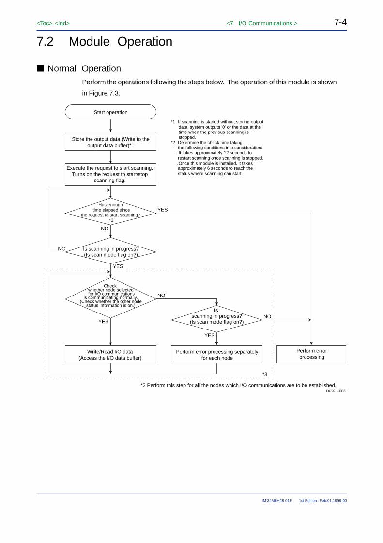
Normal OperationPerform the operations following the steps below. The operation of this module is shown
in Figure 7.3.
*1 If scanning is started without storing output data, system outputs '0' or the data at the time when the previous scanning is stopped.
*2 Determine the check time takingthe following conditions into consideration:
. It takes approximately 12 seconds to restart scanning once scanning is stopped.. Once this module is installed, it takes approximately 6 seconds to reach the status where scanning can start.
Start operation
Is scanning in progress?(Is scan mode flag on?)
Check whether node selected for I/O communications
is communicating normally.(Check whether the other node
status information is on.)
Store the output data (Write to theoutput data buffer)*1
Execute the request to start scanning.Turns on the request to start/stop
scanning flag.
Write/Read I/O data (Access the I/O data buffer)
NO
YES
YES
YES
NO
Perform error processing separatelyfor each node
Perform errorprocessing
Is scanning in progress?
(Is scan mode flag on?)
YES
NO
NO
*3
*3 Perform this step for all the nodes which I/O communications are to be established.
Has enough time elapsed since
the request to start scanning? *2
F0702-1.EPS

<Toc> <Ind> <7. I/O Communications > 7-5
IM 34M6H28-01E 1st Edition : Feb.01,1999-00
Store output data
Request to start scan
Confirm that scanning is in progress
Access I/O data
Request to stopscanning
Stop scanning confirmation
Request to start/stop scanning
Scan status
Status of othernodes
Input data buffer
Output data buffer
Scanning starts
Scan(I/O
communications)
Scanning stops
CPU module
Operation from program
This module
Interface Action
F0703.EPS
Figure 7.3 Operation Sequence and Operation of Module
Error processing during scanningIf an error occurs during I/O communications, two operation modes are provided as op-tions, namely continue/ stop. During I/O communications, information possessed by theslave may not be in agreement with the information of the scan list, or the stop/continueoperation can be specified when a slave is absent.
If "continue" is specified, communication continues with the slaves other than the one inwhich the error has occurred. Communication automatically resumes when the slave inwhich the error has occurred becomes available again. However, the red NS LED contin-ues to blink until scanning stops (see Section 4.5, "Displays Panels," in this document.)
Slave operation when communication stops varies with the specifications of the slave.
Check the specification of the slave.
Ensuring data concurrencyI/O data are concurrent in every input/output data register (1 word). There are flags thatensure data concurrency in all nodes when handling data that exceed 2 bytes, for instance,when concurrency is required between NC data and data of a barcode reader or betweenmultiple data, etc. However, concurrency should be ensured when the slave transmits thedata.
• Input Data
Flags
• Request to Prohibit Input Data Update flag in control flag of each node
• Input Data Update Status flag in status flag of each node

7-6<Toc> <Ind> <7. I/O Communications >
IM 34M6H28-01E 1st Edition : Feb.01,1999-00
Operation from Ladder/BASIC program of CPU module
1. When you wish to read the data, turn on the "request to prohibit input data update flag"of the target node.
2. Wait until the update status flag turns on. When it does, read the data and turn off theprohibit update flag.
Actions of the module
1. Confirms the request flag at the time of I/O communications to the target node. If it ison, updates to the latest input data, turns on the update status flag and enters the stopmode. Henceforth, the prohibit update flag is checked following the I/O communica-tions timing of the target node and if it is found to be on, the input data are not up-dated.
2. When the prohibit update request turns off, turn off the update status flag and updatethe input data.
CPU module This module
User program
Concurrent access to data
Exit
NO
YES
Request to prohibit updating input
data on
Input data
Request to prohibitupdating input
data on
Control flagof the node
Status flag of the node
Updating inputdata status flag
Hasupdatingstopped?
Request to prohibit updating input
data off
I/O of targetnode
Exit
Hasupdatingstopped?
YES
NO
YES
NORequset to prohibit
updating on?
Updatestatus flag
Update inputdata
NO
YES
Request toprohibit
updatingoff?
Updatestatus flag
Update inputdata
Interface I/O communication
Read input data
F0704.EPS
Figure 7.4 Ensuring Concurrency of Input Data

<Toc> <Ind> <7. I/O Communications > 7-7
IM 34M6H28-01E 1st Edition : Feb.01,1999-00
• Output Data
Flags
• Request to Prohibit Output Data Access flag in control flag of each node.
• Output Data Access Status flag in status flag of each node.
Operation from Ladder/BASIC program of CPU module
1. When you wish to output new data, turn on the request to prohibit output data accessflag of the target node.
2. Wait until the access status flag turns on, write the output data in the output data areaand turn off the request to prohibit access flag.
Actions of the module
1. If the request to prohibit access flag is on during I/O communications to the targetnode, the previous data are transmitted to the slave. If in the output data access stopmode, the access status flag is turned on.
2. When the request to prohibit access flag is off, access prohibition is cancelled, theaccess status flag is turned off and the new output data are transmitted to the slave.

7-8<Toc> <Ind> <7. I/O Communications >
IM 34M6H28-01E 1st Edition : Feb.01,1999-00
CPU module This module
Concurrent access to data
Exit
Request to prohibit access on
YES
NO
NO
YES
Output data
Request to prohibitoutput data access
Control flag of the node
Status flag of the node
Output data accessstatus flag
Has access
stopped?
Write output data
Request to prohibit
access off
I/O communications of target node
Exit
Has accessingstopped?
YES
NO
YES
NORequest toprohibit
access on?
Access status flag on
NO
YES
Request to prohibit update off?
Access status flag off
Transmit new output data
Transmit previousoutput data
Interface I/O communicationUser program
During request to
prohibit access?
F0705.EPS
Figure 7.5 Ensuring Concurrency of Output Data.

<Toc> <Ind> <7. I/O Communications > 7-9
IM 34M6H28-01E 1st Edition : Feb.01,1999-00
High order/ low order byte swapping of multiple byte data
The encoding rules are different for data on the FA-M3 and DeviceNet. Hence in multiple-byte data it is necessary to swap the high order/low order bytes every 2 bytes.
Examples are shown in Figures 7.6 and 7.7. For programming, see Section 7.6, “I/O DataAccess (Example of Programming).”
$00
$00 $01
DeviceNet
$78 $56 $34 $12 "A" "B" Other node
$01
$78 $56
$34 $12
"A"
500
Data location number
This module
501
502
503 "B"
$01 $00
$56 $78
$12 $34
"A"
D0100
Data register number
When reading data from this module, it is necessary to swap the high order/low orderbytes using a ladder or BASIC program
Input data. 16 bit integer (bit string): $0100. 32 bit integer (bit string): $12345678. 1 byte character : "A". 1 byte character : "B"
CPU module
D0101
D0102
D0103 "B"F0706.EPS
Figure 7.6 Example of Swapping of Input Data
$00
$00 $01
DeviceNet
$78 $56 $34 $12 "A" "B"Other node
$01
$78 $56
$34 $12
"A"
1000
I/O data location number
This module
1001
1002
1003 "B"
$01 $00
$56 $78
$12 $34
"A"
D0100
Data register number
When writing data into this module, it is necessary to swap the high order/low order bytes using a Ladder or BASIC program.
Output data. 16 bit integer (bit string): $0100. 32 bit integer (bit string): $12345678.1 byte character string : "A".1 byte character string : "B"
CPU module
D0101
D0102
D0103 "B"
F0707.EPS
Figure 7.7 Example of Swapping of Output Data

7-10<Toc> <Ind> <7. I/O Communications >
IM 34M6H28-01E 1st Edition : Feb.01,1999-00
7.3 Transmission Time IntervalsThe transmission time interval is the period in which I/O communications are performedcyclically. The interval can be specified in the range of 0 to 5000 ms in units of 5 ms usingthe tool commands. The setup value and value measured at the time of actual operation(measured value) can be stored in the module information of the I/O data register and read.It can also be read using the tool command.
As the transmission time interval not only depends on the number of nodes connected, thetype of communication and the capacity of data but also on the performance of the moduleand the response time of each connected device, it cannot be determined theoretically.
Perform the transmission under actual operating conditions and set a value which is largerthan the measured value of the transmission time interval. If the measured value is un-steady, then set it to the maximum measured value.
If there is a delayed response from the slave, and if there were no response when thetransmission completes, a situation occurs which is as if the slave were not present at all.In such a case set a long enough transmission time interval.
When the time needed for the transmission to all nodes is greater than the set value, thenoperate it with a time period that is larger than the set value.
The standard transmission time intervals for a single master configuration with data rate of500 kbps are displayed in Table 7.1.
Table 7.1 Standard Transmission Time Intervals
T0701.EPS
Number of slave nodes Transmission time interval (ms)
Up to 9 10
Up to 23 20
Up to 37 30
Up to 51 40
Up to 63 50

<Toc> <Ind> <7. I/O Communications > 7-11
IM 34M6H28-01E 1st Edition : Feb.01,1999-00
7.4 I/O Response TimeThe I/O response time is the time from the start of input to the slave, followed by ladderprogram processing, until output from the slave.
From a ladder program, read the input data from this module using the special module readcommand READ. Perform the required processing and write the output data to the moduleusing the special module write command WRITE. The maximum I/O response time re-quired for the above processing is estimated as follows.
Maximum I/O response time = transmission time interval 3 2 + 1 scan time
+ input delay in slave + output delay in slave
It is the same whether the transmission time interval is longer or the time for one scanis longer.
CPU module
This module
I/O transmission
I/O response delay
One scan
Transmission time interval
F0708.EPS
Figure 7.8 Maximum I/O Response

7-12<Toc> <Ind> <7. I/O Communications >
IM 34M6H28-01E 1st Edition : Feb.01,1999-00
7.5 Start/Stop Operation and Status Management(Example of Programming)This sample program shows how to start/stop an operation and how to manage the status.
This sample program is based on the following conditions:
• This module is installed in the 4th slot.
• The scan list is registered.
• The sample program is executed only when all the nodes registered in the scan listare communicating normally. (The scanning stops when a transmission error occursin any node.)
• The sample program stops when normal communication for all nodes is not achieved20 seconds after turning ON the power supply.
This sample program is described separately in:
(1) Section 7.6, “I/O Data Access” (Example of Programming)
(2) Section 8.1, “Module Operation,” and
(3) Section 8.3, “Sample Program.”
Consult these sections for more details.

<Toc> <Ind> <7. I/O Communications > 7-13
IM 34M6H28-01E 1st Edition : Feb.01,1999-00
Example of Ladder Programming
D0100
(0001)
(0002) 00001
(0003) 00003
(0004)
(0005) 00005
(0006)
(0007)
(0008)
(0009) 00007
(0010) 00009
(0011)
(0012) 00018
(0013)
(0014)
(0015)
(0016)
(0017)
(0018)
(0019) 00030
(0020)
(0021)
********Initialization/Clear error********
********Set scan operation mode********
********Set Initial output data********
********Start********
********I/O data access and message communication********
********Stop********
SET
RST
SET
M0035
X00417
M0035
M0035
X00401
X00409
X00402 X00403 X00407 I00002
I00001
Y00449
Y00449
Y00442
SET
TIM
Y00441
SET I00002
RST Y00441
20sT0001
4D0100214READ
2D0110174READ
4D0112294READ
X00409
I00003
T0001
I0002
4D0104254READ
D0106D0102D0104= =
Request to clear error flag on
Confirm clear error has completed, thenturn OFF the Error Request flag.
Set scan operation mode(on communication error, stop scan mode).
Read scan list information.
Turn on the Request to start scanningflag after confirming that there are noerrors.
Confirm scanning, and if scanning is inprocess, read the status information of other nodes.Compare scan list information and statusinformation of other nodes and if they are thesame, turn on the data valid flag (I00001) ofall the nodes.
Set status monitor timer.
Stops monitor timer.
Turn off the request to start scannigwhere there is an error in external request(I00003), monitor timer timeout, or scanning.
Error code confirmation
Confirm the node address in error.
When it is necessary to set output data before starting thescanning, see Section 7.6,“I/O Data Access (Example of Programming).”
. See Section 7.6, “I/O Data Access (Example of Programming).”
. See Section 8.3, “Sample Program (Message Communication).”
F0705-1.EPS

7-14<Toc> <Ind> <7. I/O Communications >
IM 34M6H28-01E 1st Edition : Feb.01,1999-00
Example of BASIC Programming
10 ! **********************************************************
20 ! * F3LD01-ON SAMPLE PROGRAM
30 ! * Start/Stop Operation and Status Management
40 ! **********************************************************
50 ! ****Initial setup****
60 DEFINT A-Z
70 DIM DLIST (3), DSTS (3)
80 LDSLOT = 4
90 ASSIGN LD01 = LDSLOT
100 !
110 !****Initialization Clear Error****
120 CONTROL LDSLOT, 102; $0001, $FFFF : ! Request to Clear Error (Y 49)
on, and other relays off
130 CONTROL LDSLOT, 101; $0000, $FFFF : ! Other relays off
140 STS=0
150 WHILE BIT (STS, 0) = 0 : ! Wait till Clear Error Confirmation
(X 17) is turned ON
160 STATUS LDSLOT, 102; STS
170 END WHILE
180 CONTROL LDSLOT, 102; $0000, $0001 : ! Request to clear Error (Y 49)
is off
190 !
200 ! **** Preparations for the operation ****210 ON TIMER #1,20000 GOTO ERROR@ : ! set 20 second timer
220 !
230 FOR I=0 TO 3 : ! Read scan list
240 ENTER LDSLOT, 21+I NOFORMAT;DLIST (I)
250 NEXT I
260 !
270 !
280 GOSUB DWRITE@ : ! Write output data
290 !
400 !****Start operation****
410 CONTROL LDSLOT,101; $0200,$0200 : ! Set scan operation mode (Y
42 ON)
420 CONTROL LDSLOT,101; $0100,$0100 : ! Request to start scanning (Y 41
ON)
430 !
440 LOOP1@
450 STS=0
460 STATUS LDSLOT,101;STS : ! Wait till X 9 turns on
470 SCANON=BIT(STS,8)
480 IF SCANON<>1 THEN LOOP1@
490 FOR I=0 TO 3 :! Confirm the status information of
other nodes

<Toc> <Ind> <7. I/O Communications > 7-15
IM 34M6H28-01E 1st Edition : Feb.01,1999-00
500 ENTER LDSLOT,25+I NOFORMAT;DSTS (I)
510 IF DLIST (I) <> DSTS (I) THEN LOOP1@ : ! Compare with scan list (Wait
till it matches)
520 NEXT I
530 !
540 !
600 ! ****Valid data****
610 OFF TIMER #1 : ! 20 second timer interrupt off
620 !
630 GOSUB MESSEGE@ : ! Message Communication request
640 !
650 LOOP2@
660 STS=0
670 STATUS LDSLOT,101;STS : ! Confirm that X 9 is ON
680 SCANON=BIT (STS,8)
690 IF SCANON=0 THEN ERROR@
700 !
720 GOSUB DREAD@ : ! Read input data
730 GOSUB DWRITE@ : ! Write output data
740 GOTO LOOP2@ : ! Repeat the execution during
scanning
750 !
800 ! **** Error processing **** : ! Error processing
810 ERROR@
820 ENTER LDSLOT,17 NOFORMAT;ERCODE1
830 ENTER LDSLOT,18 NOFORMAT;ERCODE2
840 ENTER LDSLOT,29 NOFORMAT;ERCODE1 : ! ead the node address in error
850 ENTER LDSLOT,30 NOFORMAT;ERCODE2
860 ENTER LDSLOT,31 NOFORMAT;ERCODE3
870 ENTER LDSLOT,32 NOFORMAT;ERCODE4
880 DP "ERCODE1=",HEX$ (ERCODE1) : ! Error code 1(hexadecimal
display)
890 DP "ERCODE2=",HEX$ (ERCODE2) : ! Error code 2(hexadecimal
display)
900 DP "ERCODE1=",HEX$ (ERCODE1) : ! Display error node
(hexadecimaldisplay)
910 DP "ERCODE2=",HEX$ (ERCODE2)
920 DP "ERCODE3=",HEX$ (ERCODE3)
930 DP "ERCODE4=",HEX$ (ERCODE4)
940 CONTROL LDSLOT, 101;$0000,$FFFF : ! Request to stop scanning
950 STOP
3000 END

7-16<Toc> <Ind> <7. I/O Communications >
IM 34M6H28-01E
7.6 I/O Data Access (Example of Programming)A programming example of I/O data access is shown below. In this program, the scan list isregistered in the input and output data areas and normal communication is performed.
Input data
T0706-1.EPS
Data position no.
Data typeData register
(used in Ladder)Input variable
(used in BASIC)High order 8 bits Low order 8 bits
510 Word data D0001 IN1
511 Word data D0002 IN2
512 Word data D0003 IN3
513 Unused Byte data D0004 IN4
Output data
T0706-2.EPS
Data position no.
Data typeData register
(used in Ladder)Input variable
(used in BASIC)High order 8 bits Low order 8 bits
1021 Word data D0011 OUT1
1022 Word data D0012 OUT 2
1023 Word data D0013 OUT 3
1024 Unused Byte data D0014 OUT 4
1st Edition : Feb.01,1999-00
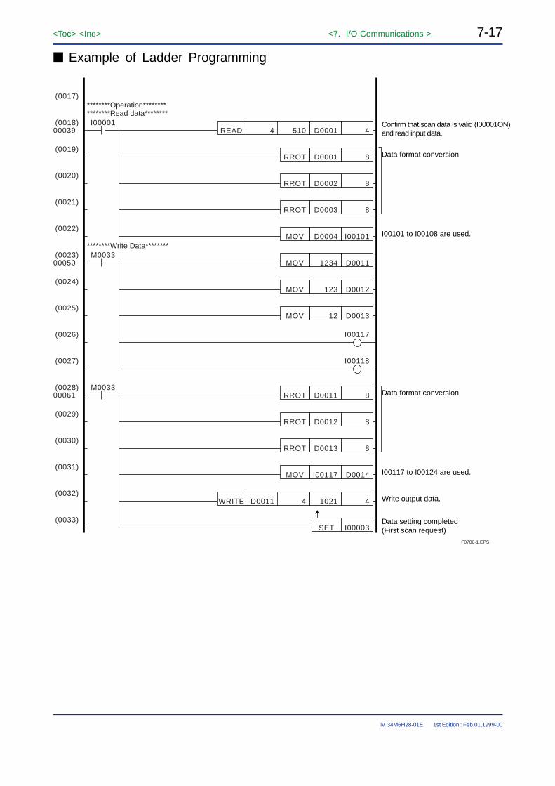
<Toc> <Ind> <7. I/O Communications > 7-17
IM 34M6H28-01E
Example of Ladder Programming
(0017)
(0018) 00039
(0019)
(0020)
(0021)
(0022)
(0023) 00050
(0024)
(0025)
(0026)
(0027)
(0028) 00061
(0029)
(0030)
(0031)
(0032)
(0033)
********Operation****************Read data********
********Write Data********
4D00015104READ
410214D0011WRITE
8D0001RROT
8D0002RROT
8D0003RROT
I00101D0004MOV
8D0011RROT
8D0012RROT
8D0013RROT
D0014I00117MOV
D00111234MOV
D0012123MOV
D001312MOV
I00001
M0033
M0033
I00117
I00118
SET I00003
Confirm that scan data is valid (I00001ON)and read input data.
Data format conversion
I00101 to I00108 are used.
Write output data.
Data setting completed(First scan request)
F0706-1.EPS
Data format conversion
I00117 to I00124 are used.
1st Edition : Feb.01,1999-00

7-18<Toc> <Ind> <7. I/O Communications >
IM 34M6H28-01E
Example of BASIC ProgrammingThis program is only a subroutine and is called from the program described in Section 7.5,“Start/Stop Operation and Status Management.”
1000 ! **** Read input data ****1010 DREAD@
1020 ENTER LDSLOT ,511 NOFORMAT ;IN1 : ! Read input data
1030 IN1=ROTATE(IN1,8) : ! Data 8-bit rotate
1040 ENTER LDSLOT ,512 NOFORMAT ;IN2
1050 IN2=ROTATE(IN2,8)
1060 ENTER LDSLOT ,513 NOFORMAT ;IN3
1070 IN3=ROTATE(IN3,8)
1080 ENTER LDSLOT ,514 NOFORMAT ;IN4
1090 IN4=BINAND ($FF00,IN4) : ! High order 8-bit truncation
1100 RETURN
1200 ! ****Write output data****
1210 DWRITE@
1220 OUT1=1234
1230 OUT2=123
1240 OUT3=12
1250 OUT4=2
1260 OUT=ROTATE(OUT1,8) : ! Data 8-bit rotation
1270 OUT=ROTATE(OUT2,8)
1280 OUT3=ROTATE(OUT3,8)
1290 OUTPUT LDSLOT, 1021 NOFORMAT ;OUT1 : ! Write output data
1300 OUTPUT LDSLOT, 1022 NOFORMAT ;OUT2
1310 OUTPUT LDSLOT, 1023 NOFORMAT ;OUT3
1320 OUTPUT LDSLOT, 1024 NOFORMAT ;OUT4
1st Edition : Feb.01,1999-00

<Toc> <Ind> <8. Message Communications > 8-1
IM 34M6H28-01E 1st Edition : Feb.01,1999-00
8. Message CommunicationsIn this section, operation of message communications in this module and the interface isexplained.
8.1 Module OperationOperation during message communications in this module are explained here.
Conditions for request to receive communicationWhen the following conditions are satisfied, a request to receive communication is transmit-ted.
• "Message communications" are registered in the communications type of the targetnode in the scan list.
• Scanning is in process
• The target node and the node information match and communication is in progress.
Transmission procedureUse the CPU module's Ladder/BASIC program and follow the procedure below for commu-nication.

8-2<Toc> <Ind> <8. Message Communications >
IM 34M6H28-01E 1st Edition : Feb.01,1999-00
Message transmission
End
Are both messagecommunication request and completion
flags turned off?
Is the messagecommunication completion
flag on?
Create a request message.(write to message communication
transmission buffer.)
Message communication request flag is turned on.
Read the response message (read itfrom message communication
reception buffer).
Message communication request flag is turned off.
Confirm the contents ofthe response message/exit code.
YES
NO
YES
NO
F0801-1.EPS

<Toc> <Ind> <8. Message Communications > 8-3
IM 34M6H28-01E 1st Edition : Feb.01,1999-00
Write requestmessage
Transmissionrequest
Response reception check
Read responsemessage
Requset flag off
Messagecommunication
transmission buffer
Messagecommunicationexecution flag
Messagecommunicationcompletion flag
Message communication reception buffer
Checkstransmission request Other
nodes
Transmission
Reception
Reception notice
Clears reception notice
CPU module
Ladder/BASIC program
This module
Interface Operation of this module
F0801.EPS
Figure 8.1 Transmission Procedure and Actions of the Module

8-4<Toc> <Ind> <8. Message Communications >
IM 34M6H28-01E 1st Edition : Feb.01,1999-00
8.2 Interface
8.2.1 Request and Response FormatsThe request and response formats in the message communication transmit/receive buffer
are as follows:
• Request
Data position no. Contents
1501 0 (reserved)
1502 Transmission destination node address
1503 0
1504 0
1505 Size of service data (number of bytes)
1506 Service code specified for DeviceNet
1507 Class ID of transmission destination
1508 Instance ID of transmission destination
1509 (up to 1550) Service data
T080201-1.EPS
• Response message
T080201-2.EPS
Data position no. Contents
1551 0 (reserved)
1552 Response source node address
1553 Exit code
1554 0 (reserved)
1555 Size of service data (number of bytes)
1556 Service code specified for DeviceNet
1557 (up to 1600) Service data
• Limit of service data size• Service data (for Request) has a maximum of 84 bytes.
• When service data (for Response Messages) exceeds 88 bytes, code for "abnormalexit" is stored in the exit code area of the response. In such situations, the first 88bytes of the service data is kept in the response message.
• High order / low order byte swapping of multiple-byte data in service dataThe encoding rules are different for data on FA-M3 and DeviceNet. Hence, in multi-bytedata, it is necessary to swap the byte high order/ low order byte every 2 bytes.
See also Section 7.2, “Module Operation.”
SEE ALSO
For information on the service code, service data, class ID and instance ID, refer to the “DeviceNetSpecification” published by ODVA.

<Toc> <Ind> <8. Message Communications > 8-5
IM 34M6H28-01E 1st Edition : Feb.01,1999-00
8.2.2 Exit CodesThe exit codes used for message communications are described herein.
T080202-1.EPS
Error code Description Troubleshooting
$0100Connection for message communications is unavailable.
Target node may be absent or message communications are not registered as communication type in scan list. Confirm the network status and device list.
$0101 Parameter error (Class ID) Class ID specification area for target node is less than or equal to 255, but a value above 256 is specified. Specify a valid value.
$0102 Parameter error (instance ID) Instance ID specification range for the target node is less than or equal to 255, but a value above 256 is specified. Specify a valid value.
$F101 Receive buffer size overflow for response message
Normal receive is not possible for this service. First 88 bytes of the service data is stored in receive buffer.
$F102 Parameter error (node address) Specify the correct node address in the range from 0 to 63.
$E112 Network power failure during communications
See error codes (see Section 10, “Errors and Troubleshooting”).
$E144 No response from target device (timeout)
See error codes (see Section 10, “Errors and Troubleshooting”).

8-6<Toc> <Ind> <8. Message Communications >
IM 34M6H28-01E 1st Edition : Feb.01,1999-00
8.3 Sample ProgramsRemote setting of operation (output cut-off/maintain) during abnormal communications of adiscrete output device is given as a sample program of message communications.
The target device supports the following services and attributes.
• Service
SetAttribute_Single (DeviceNet common service, $10)
• Attribute
Class ID = 9, Instance ID = 1, Attribute ID = 5
(Prescribed attribute value for operation during a communication error)
• Setup value
8-bit integer (0 = Cut off, 1 = Maintain)
Message request format
T0803-1.EPS
Data position no. Data Contents
1501 0 Reserved
1502 1 Transmission destination node address
1503 0 Reserved
1504 0 Reserved
1505 2 Service data size (byte)
1506 $10 Service code "Set_Attribute_Single"
1507 9 Class ID
1508 1 Instance ID
1509 High-order 8 bits $05 Service data Attribute ID, 5
1509 Low-order 8 bits $01 Service data Setup value, 1
Message response format (during normal exit)
T0803-2.EPS
Data position no. Data Contents
1551 0 Reserved
1552 1 Transmission destination node address, 1
1553 0 Error code, 0
1554 0 Reserved
1555 0 Size of service data, 0 byte
1556 $90 Service code ($80 + service code)

<Toc> <Ind> <8. Message Communications > 8-7
IM 34M6H28-01E 1st Edition : Feb.01,1999-00
Example of Ladder ProgrammingOnly message communications are given in this program. Use it with the program given in
Section 7.5, “Start/Stop Operation and Status Management.”
(0034)
(0035) 00074
00104
(0036)
(0037)
(0038)
(0039)
(0040)
(0041)
(0042)
(0043)
(0044)
(0045)
(0046)
(0047)
(0048)
(0049)
(0052)
********Message communication********
1150140WRITE
1D01502914READ
D0100$0501MOV
I00200 I00001
1150241WRITE
1150340WRITE
1150440WRITE
1150544WRITE
115064$10WRITE
1150749WRITE
1150841WRITE
215094D0100WRITE
119141WRITE
(0050) 6D015015514READ
I0200
I00200
1=D0150
RST
(0051) 119140WRITE
I00200, Message communication start relay I00001, confirm communication status.(Refer to 7.5 “start/stop Operation and Status Management” (Example of programming)
Reserved
Message receiver Setting node address
Reserve
Reserve
Service data size (Byte)
Service code(Set_Attribute_Single)
Class ID
Instance ID
Service data
F0803-1.EPS
Write service data.
Message communication requeston
Confirm message status flag.
Read response after confirming completion of message communications.
Message communication requestoff

8-8<Toc> <Ind> <8. Message Communications >
IM 34M6H28-01E 1st Edition : Feb.01,1999-00
Example of BASIC ProgrammingThis program is only a subroutine and can be called from the program described in
Section 7.5, “Start/Stop Operation and Status Management.”
2000 ! ****Message communication****
2010 MESSEGE@
2020 OUTPUT LDSLOT ,1501 NOFORMAT ;0 : ! Reserved
2030 OUTPUT LDSLOT ,1502 NOFORMAT ;1 : ! Node number
2040 OUTPUT LDSLOT ,1503 NOFORMAT ;0 : ! Reserved
2050 OUTPUT LDSLOT ,1504 NOFORMAT ;0 : ! Reserved
2060 OUTPUT LDSLOT ,1505 NOFORMAT ;2 : ! Service data size (Byte)
2070 OUTPUT LDSLOT ,1506 NOFORMAT ;$10 : ! Service code2080
OUTPUT LDSLOT ,1507 NOFORMAT ;9 : ! Class ID
2090 OUTPUT LDSLOT ,1508 NOFORMAT ;1 : ! Instance ID
2100 SEND1=$0501 : ! Service data
2140 OUTPUT LDSLOT ,1509 NOFORMAT ;SEND1 : ! Write service data
2150 OUTPUT LDSLOT ,1510 NOFORMAT ;SEND2 : !
2160 OUTPUT LDSLOT ,191 NOFORMAT ;1 : !Message communication request
2170 !
2180 MSTS=0
2190 WHILE MSTS=0 : ! Wait till message status flag
turns ON
2200 ENTER LDSLOT 291, NOFORMAT ;MSTS
2210 END WHILE
2220 ENTER LDSLOT ,1551 NOFORMAT ;MSG1 : ! Read response
2230 ENTER LDSLOT ,1552 NOFORMAT ;MSG2
2240 ENTER LDSLOT ,1553 NOFORMAT ;MSG3
2250 ENTER LDSLOT ,1554 NOFORMAT ;MSG4
2260 ENTER LDSLOT ,1555 NOFORMAT ;MSG5
2270 ENTER LDSLOT ,1556 NOFORMAT ;MSG6
2280 !
2290 OUTPUT LDSLOT ,191 NOFORMAT ;0 : ! Release Message Comm. Request
2300 RETURN

<Toc> <Ind> <9. Configuration > 9-1
IM 34M6H28-01E 1st Edition : Feb.01,1999-00
9. ConfigurationConfiguration includes the following:
• Creating a scan list
• Registering the transmission time interval
• Storing in flash memory
• Remote setting of other nodes (see Section 8.3, “Sample Programs,” in this manual)
Configuration is performed by starting the Ladder/BASIC program for setting configurationon the CPU module which is defined when this module is used. Configuration is confirmedusing Ladder Diagram Support Program Tool M3 or BASIC Programming Tool M3.
9.1 Tool CommandsTool command are an interface that can be used to define the actions of this module usingthe Ladder/BASIC program when preparing for operation.
Please do not use the tool commands during operation.
9.1.1 CommandsTool commands are given in Table 9.1.
Table 9.1 Commands
Command no. Command
$03 Register Device (Scan List)
$04 Read Device (Scan List)
$05 Delete Device (Scan List)
$71 Store Flash Memory (Transmission Time Interval/Scan List)
$72 Register Transmission Time Interval
$73 Read Master Information
T0901.EPS

9-2<Toc> <Ind> <9. Configuration >
IM 34M6H28-01E 1st Edition : Feb.01,1999-00
9.1.2 Request ProcedureThe request procedure for the tool commands is given below.
Tool command execution
End
F090102-1.EPS
Are both tool request to execute command
flag and completion flag off?
Is the tool command execution completion flag on?
Creating the requested command(writing command to tool command
buffer)
Turns on tool request to execute command flag
Reads the response (reads theresponse from tool command buffer)
Turns off tool request to execute command flag
Confirms the contents of response/exitcode
YES
NO
YES
NO

<Toc> <Ind> <9. Configuration > 9-3
IM 34M6H28-01E 1st Edition : Feb.01,1999-00
Writing requested command
Execute request
Completion check
Reading response
Request flag off
Tool request to execute command flag Y 58
Tool command execution completion flag X 26
Tool command buffer
Checks request
Command execution
Completion notification (flag on)
Request off checkcompletion flag off
CPU module
Ladder/BASIC program
This module
Interface Action within this module
F0901.EPS
Figure 9.1 Tool Command Request Procedures and Actions of the Module

9-4<Toc> <Ind> <9. Configuration >
IM 34M6H28-01E 1st Edition : Feb.01,1999-00
9.1.3 Basic Command FormatsThe format for a request/response (normal exit/error exit) is given below.
• Request
Data position no. Content
400 Command number
401 to 449 Parameters
T090103-1.EPS
• Response (normal exit)
T090103-2.EPS
Data position no. Content
400 Command number
401 to 449 Parameters
• Response (error exit)
Data position no. Content
400 Command number+$8000
401 Exit code
T090103-3.EPS
TIP
The tool command buffer uses the same area for requests and responses.

<Toc> <Ind> <9. Configuration > 9-5
IM 34M6H28-01E 1st Edition : Feb.01,1999-00
9.1.4 Details of Commands
1) Register deviceRegisters device information for each node in the scan list. Nodes already registeredcannot be registered again. Perform registration after deleting the devices and emptyingthe information in the scan list.
• Request
Data position no. Content
400 Command = $03
401 Node number
402 Vendor ID
403 Device type
404 Product code
405-407 Reserved
408 Communications type
409-411 Reserved
412 Size of output data (bytes)
413 Offset of output data (bytes)
414-415 Reserved
416 Size of input data (bytes)
417 Offset of input data (bytes)
418-426 Reserved
T090104-1.EPS
• Response (normal exit)
T090104-2.EPS
Data position no. Content
400 Command = $03
• Response (error exit)
T090104-3.EPS
Data position no. Content
400 $8003
401 Exit code
• Supplement
• Set reserved area to 0.
• Communications type
Use only one method of I/O communications. Both I/O communications and messagecommunications can be selected.
F090104-1.EPS
R R R R R R ST P EX
15 7 0

9-6<Toc> <Ind> <9. Configuration >
IM 34M6H28-01E 1st Edition : Feb.01,1999-00
R: System reserved
EX: Message communications
P: I/O communications: Polling
ST: I/O communications : Bit strobe
• The I/O data offset is the relative position from the beginning of every I/O data buffer.The unit for the I/O data offset/size is bytes.
• The input data size of a Bit Strobe should be less than or equal to 8 bytes.
• Set the size/offset to 0 when no I/O communications are being carried out.
• Registration is not possible during scanning.
2) Read deviceReads device information of a node from the scan list.
• Request
T090104-4.EPS
Data position no. Content
400 Command = $04
401 Node number
• Response (normal exit)
T090104-5.EPS
Data position no. Content
400 Command = $04
401 Node number
402 Vendor ID
403 Device type
404 Product code
405-407 Reserved
408 Communications type
409-411 Reserved
412 Size of output data (bytes)
413 Offset of output data (bytes)
414-415 Reserved
416 Size of input data (bytes)
417 Offset of input data (bytes)
418-426 Reserved
• Response (error exit)
T090104-6.EPS
Data position no. Content
400 $8004
401 Exit code

<Toc> <Ind> <9. Configuration > 9-7
IM 34M6H28-01E 1st Edition : Feb.01,1999-00
• Supplement
• For information on communications type/offset, refer to the description of deviceregistration.
3) Delete deviceDeletes the device information of a node from the scan list.
• Request
T090104-7.EPS
Data position no. Content
400 Command = $05
401 Node number
• Response (normal exit)
T090104-8.EPS
Data position no. Content
400 Command = $05
• Response (error exit)
T090104-9.EPS
Data position no. Content
400 $8005
401 Exit code
• Supplement
• Deletion is not possible during scanning.
4) Store in flash memoryWrites the transmission time interval/device list to flash memory.
• Request
T090104-10.EPS
Data position no. Content
400 Command = $71
• Response (normal exit)
T090104-11.EPS
Data position no. Content
400 Command = $71

9-8<Toc> <Ind> <9. Configuration >
IM 34M6H28-01E 1st Edition : Feb.01,1999-00
• Response (error exit)
T090104-12.EPS
Data position no. Content
400 $8071
401 Exit code
• Supplement
• Writing is not possible during scanning.
5) Register transmission time intervalRegisters transmission time intervals.
• Request
T090104-13.EPS
Data position no. Content
400 Command = $72
401-402 Reserved
403 Transmission time interval [msec]
• Response (normal exit)
T090104-14.EPS
Data position no. Content
400 Command = $72
• Response (error exit)
T090104-15.EPS
Data position no. Content
400 $8072
401 Exit code
• Supplement
• Set reserved areas to 0.
• Valid range for the transmission time interval is 0 to 5000 [ms].
• Registration cannot be carried out during scanning.
6) Read master informationReads information related to the master.
• Request
T090104-16.EPS
Data position no. Content
400 Command = $73

<Toc> <Ind> <9. Configuration > 9-9
IM 34M6H28-01E 1st Edition : Feb.01,1999-00
• Response (normal exit)
T090104-16.EPS
Data position no. Content
400 Command = $73
401-402 Reserved
403 Transmission time interval [msec]
404 Reserved
405 Vendor ID
406 Device type
407 Product code
508 Revision
409 Status
410-411 Serial number
412-429 Product name
430 Reserved
• Response (error exit)
T090104-17.EPS
Data position no. Content
400 $8073
401 Exit code
• Supplement
This module keeps the module information shown in Table 9.2, in accordance with theDeviceNet specification. This information can be read using the read master informationcommand.
Table 9.2 Module Information Summary
Name Description Value of this module
Vendor ID Identifier of device manufacturer $FA
Device type Code indicating device type $C
Product code Code indicating device model 1
Revision Product revision of device *1
Status Module status of device *2
Serial number Serial number of device *3
Product name Product name of device *4
T0902.EPS
*1 The revision starts from 1.1 ($0101) in the DeviceNet manual.*2 The status codes given in the DeviceNet manual are used.*3 Each device is given a unique number.*4 FA-M3 LD01 Scanner Module

9-10<Toc> <Ind> <9. Configuration >
IM 34M6H28-01E 1st Edition : Feb.01,1999-00
9.1.5 Exit CodesThe unique exit codes used in response to tool commands are given in Table 9.3. In thecase of an incorrect response to a request, either confirm the command number/parameteror delete device/stop scanning before the request, according to the exit code.
Table 9.3 Summary of Exit Codes
Item Exit code Description
Unsupported command
$0001 The specified command is not supported.
Node number error $0002 The specified node number is beyond the range.
Device already registered
$0005 The device is already registered.
Device is not set $0006 The scan list is empty.
Scanning in progress $000A Execution is not possible during scanning.
Outside the data area range
$000D Value specified is outside the range of the I/O data area.
Communications type error
$000F The specified communications type is not supported.
Flash memory error $1283 Unable to write to flash memory due to exceeding the limit allowed for writing to flash memory.
Connection not used $8000 Offset/size are specified even though I/O communications is not selected.
Data area undefined $8001 Offset/size are not specified even though I/O communications is selected.
Duplication of data area
$E131 The data area being used is duplicated in another node.
Master information error
$E133 Beyond the range of master information parameter (transmission time interval).
T0903.EPS

<Toc> <Ind> <9. Configuration > 9-11
IM 34M6H28-01E 1st Edition : Feb.01,1999-00
9.2 Configuration ProcedureConfiguration involves the following steps:
1. Create a scan list and set the transmission time interval.
Register the nodes with which communication is to be established (create a scan list)and set the transmission time interval using the tool command. Set the transmissiontime interval to either 0 msec. or to a specific value (it is necessary to set the valuesagain using values measured during the test run).
In the sample program in Section 9.3 of this manual, the steps for registering thedevices and setting the transmission time interval are given. After the setting is done,execute the program.
2. Test Run
Start scanning and verify whether communication is taking place properly with thedevices registered in the scan list. If there is an error, check the settings, wiring, scanlist, etc. of this module and other devices, then re-adjust and set again.
Once normal communication with all the nodes is confirmed, compute the transmis-sion time interval measured value (Data position no. 8 of I/O data register) (If themeasured values are unsteady, record the maximum value).
For operation, see the sample program in Section 7.5, “Start/Stop Operation andStatus Management (Example of Programming),” in this manual.
3. Evaluate Configuration Results
If communication does not take place properly and if the measured value of thetransmission time interval (actual value during scanning) exceeds the set value, set anappropriate value again, and then test run and confirm the operation.
CAUTION
(1) In the sample program given in Section 9.3 of this manual, the processes necessaryfor configuration (Setting transmission time interval / Initialising scan list / deviceregistration / storing in flash memory) are carried out in one program. When changingthe configuration, re-run the program after making the necessary changes.
(2) The transmission time interval/scan list is stored in the flash memory all at once.Please note that this deletes all the previous data in the flash memory.

9-12<Toc> <Ind> <9. Configuration >
IM 34M6H28-01E 1st Edition : Feb.01,1999-00
9.3 Sample ProgramA sample program for configuration is given here.
Configuration is carried out as follows:
Configuration
End
F0903-1.EPS
Clear error
Setup transmission time interval
Initialize scan list
Register device
Store in flash memory
Clears the error flags of this module.
Sets up transmission time interval.
Deletes all the registered devices from the scan list.
Registers device and creates a scan list.
Stores the register scan list and transmissiontime interval in flash memory. If it is not stored in flash memory, the scan list is lost when power is switched to off.

<Toc> <Ind> <9. Configuration > 9-13
IM 34M6H28-01E 1st Edition : Feb.01,1999-00
• Clear Error
The clear error command is carried out as follows:
Clear error
End
F0903-2.EPS
Request to clear error relay (Y49) on
Clear error completed confirmation relay(X17) on
Release request to clear error relay (X49) off
Release request to clear error confirmation relay (X17) off
• Setting Transmission Time Interval
Setting the transmission time interval is carried out as shown below.
In the sample program, the transmission time interval is set to 20 ms.

9-14<Toc> <Ind> <9. Configuration >
IM 34M6H28-01E 1st Edition : Feb.01,1999-00
Setting transmission time
400 Command $72403 Set Transmission Time Interval
END
Error processing
F0903-3.EPS
Write a request to command buffer
Request to execute command relay (Y58) on
Execute command completed confirmation relay (X26) on
Read response
Release request to executecommand relay (Y58) off
Release request to execute command confirmation relay (X26) off
Any errors? (command codes of
request/response do not match)
NO
YES

<Toc> <Ind> <9. Configuration > 9-15
IM 34M6H28-01E 1st Edition : Feb.01,1999-00
• Initalizing Scan list
If there are registered devices, they are deleted from the scan list.
Deletion from the scan list is carried out in the following manner.
Initialising scan List
END
Error processing
400 Command $05401 Node address, N
F0903-4 .EPS
Write a request to command buffer
Node address N=0
Request to execute command relay (Y58) on
Execute command completed confirmation relay (X26) on
Read response
Release request to execute command relay (Y58) off
Release request to execute command confirmation relay (X26) off
N=N+1
Any errors?
Exit Code=6?
All nodes completed? N>=64
NONO
NO
YES
YES
YES
YES
YES
NO
Scan information not set relay (X07) ON?
Device Not Set (the request for deletion was for a node for whichdevice was not set, hence ExitCode=6 is normal)
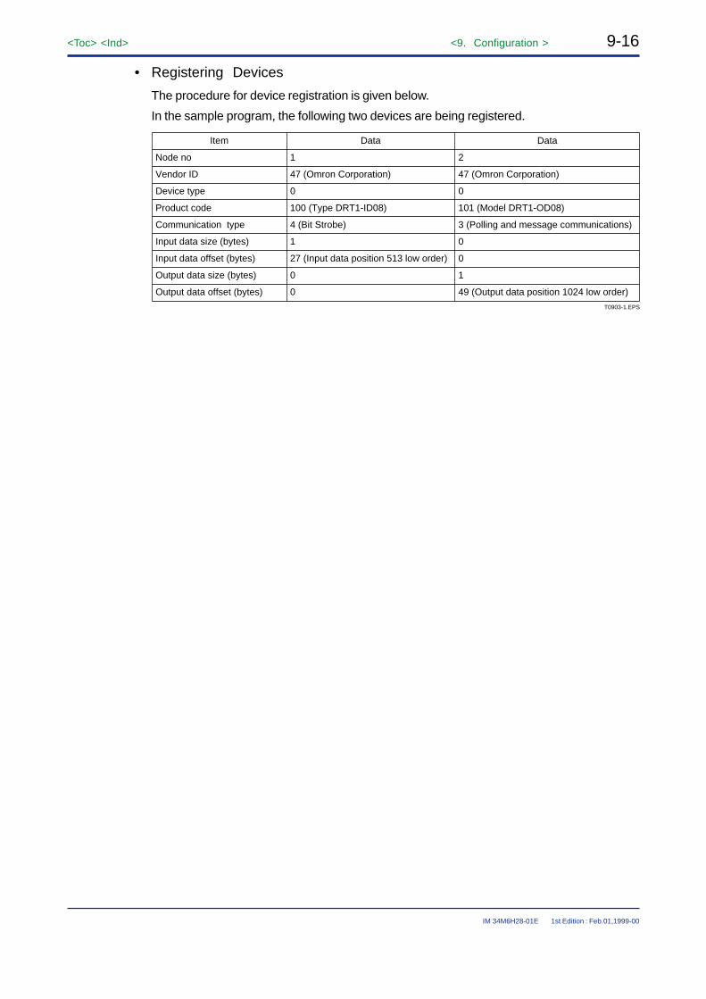
9-16<Toc> <Ind> <9. Configuration >
IM 34M6H28-01E
• Registering Devices
The procedure for device registration is given below.
In the sample program, the following two devices are being registered.
Item Data Data
Node no 1 2
Vendor ID 47 (Omron Corporation) 47 (Omron Corporation)
Device type 0 0
Product code 100 (Type DRT1-ID08) 101 (Model DRT1-OD08)
Communication type 4 (Bit Strobe) 3 (Polling and message communications)
Input data size (bytes) 1 0
0Input data offset (bytes) 27 (Input data position 513 low order)
Output data size (bytes) 0 1
Output data offset (bytes) 0 49 (Output data position 1024 low order)
T0903-1.EPS
1st Edition : Feb.01,1999-00

<Toc> <Ind> <9. Configuration > 9-17
IM 34M6H28-01E
Registering devices
400 Command $03401 or greater - Registration information
Error processing
Write a request to command buffer
Reads the data of registered slave one by one.Read device registration data
Request to execute command relay (Y58) on
Execute command completed confirmation relay (X26) on
Read response
Request to execute command relay (Y58) off
Execute command completed confirmation relay (X26) off
Any errors?
NO
YES
Is data available?
YES
NO
END
F0903-5.EPS
1st Edition : Feb.01,1999-00
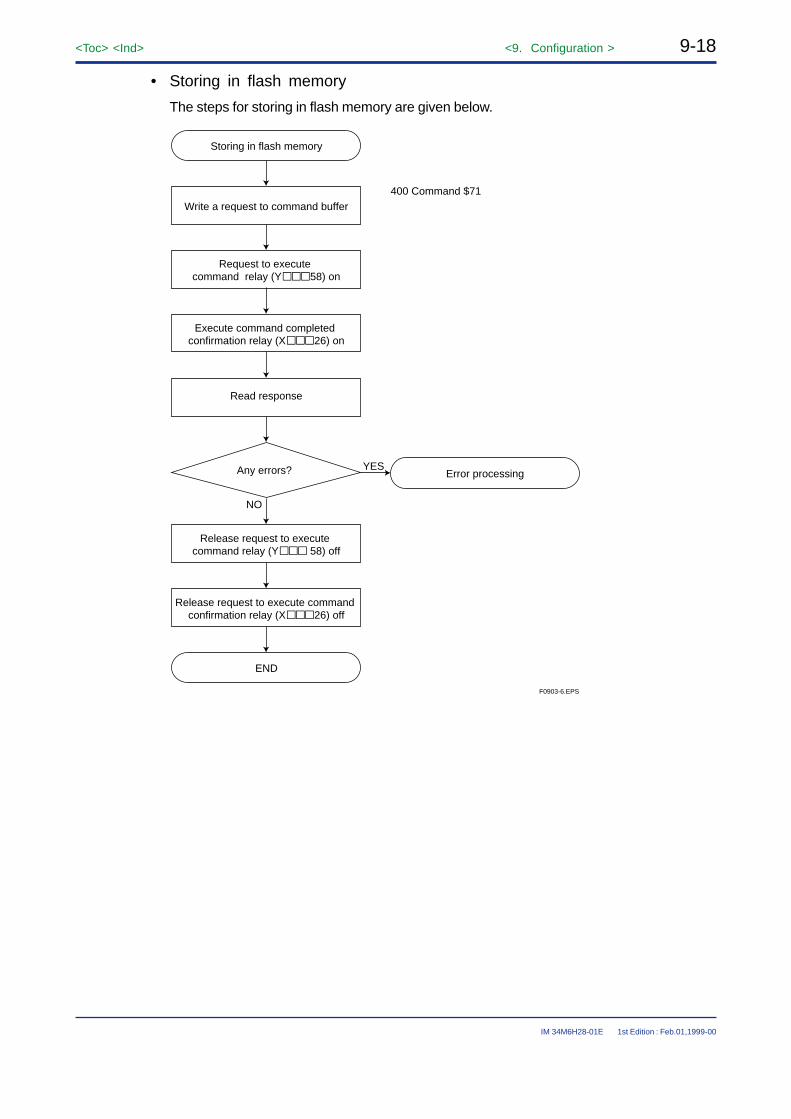
9-18<Toc> <Ind> <9. Configuration >
IM 34M6H28-01E
• Storing in flash memory
The steps for storing in flash memory are given below.
Storing in flash memory
400 Command $71
END
Error processing
F0903-6.EPS
Write a request to command buffer
Request to execute command relay (Y58) on
Execute command completed confirmation relay (X26) on
Read response
Release request to execute command relay (Y 58) off
Release request to execute command confirmation relay (X26) off
Any errors?
NO
YES
1st Edition : Feb.01,1999-00

<Toc> <Ind> <9. Configuration > 9-19
IM 34M6H28-01E
Sample Program Using Ladder ProgramA sample program using ladder programs is shown here. The sample program is createdbased on the following conditions.
• This module is installed in slot 4.
• The contents for device registration should be set in advance as given below.
D0051 ~ information for first item
D0101 ~ information for second item
D0051+503N information for Nth item
Set -1 at the end of the data.
• Handling internal register
D0001 = 6 Normal exit
D0001 = 7 Error has occurred
D0011: Process number where an error has occurred
D0012: Node address where an error has occurred (during device deletion)
Information of (N-1)th device where an error has occurred (duringdevice registration)
D0013: Command where an error has occurred ($8000+command number)
D0014: Exit code when an error has occurred
1st Edition : Feb.01,1999-00

9-20<Toc> <Ind> <9. Configuration >
IM 34M6H28-01E
(0002)
(0001)
(0003)
00001
(0004)
(0005)
(0006)
(0007)
(0008) 00012
00014(0009)
(0010)
(0011)
(0012)
(0013)
00019
********Initialisation ********
********Clear error********
********Execute command********
2048D00010BSET
1200D20490BSET
D00074MOV
I000010MOV
Y00433MOV
Y00449SET
D00011MOV
M0035
M0035
Y00449RSTM00417
Y00458SET
I00001RST
I00001 X00426
0
Clear data register.
Clear Y relay of this module.
Clear relay.
Specify the slot number of this module.
Clear error request on.
Confirm that clear error has completed,and then clear error request off.
Go to next processing.
F0903-7.EPS
Request to execute command.
1st Edition : Feb.01,1999-00

<Toc> <Ind> <9. Configuration > 9-21
IM 34M6H28-01E
(0015)
(0014)
(0016)
00025
(0017)
(0018)
(0019)
(0020)
(0021)
00032
(0022)
(0023)
(0024)
(0025)
(0026) 00055
00062
********Setting transmission time interval********
********Check that device is not registered********
********Delete device********
2D0003400D0007READ
50400D00070WRITE
1400D0007$72WRITE
1403D000720WRITE
X00426
Y00458RST
I00002SET
I00001SET
D0001INC
(0027)
(0028)
(0029)
(0030)
(0031)
(0032)
(0033)
(0034)
(0035)
(0036)
I000021=D0001
X004072=D0001
$72=D0003
I00006SET
I00002RST
$72<>D0003
I00002
50400D00070WRITE
1400D00075WRITE
14014D0002WRITE
I00001SET
I000023=D0001
D0002INC5=D0003
6=D0004
I00006SETD0006=D0002
I00002
4MOV
X004073MOV
D0001
D0001
D0002MOV D0006
Request to execute command off.
Clear tool command buffer.
Command $72
Set transmission time interval to 20ms.
Request to execute command.
Proceed to next processing on normal exit.
Confirm that command execution hascompleted, and then read response.
Proceed to error processing on error.
Clear tool command buffer.
Tool comand $5
Specify node address to be deleted.
Command request
Keep the node address specified earlier.
Proceed to next node address on normal exitDo not change node address on error.
Proceed to error processing if node address is not changed (i.e., if error has occurred).
F0903-8.EPS
Proceed to device registration if device is not registered.
Proceed to device deletion if device is registered.
1st Edition : Feb.01,1999-00

9-22<Toc> <Ind> <9. Configuration >
IM 34M6H28-01E
(0038)
(0037)
(0039)
(0040)
(0041)
(0042)
(0043)
(0044)
00093
00110(0045)
(0046)
(0047)
(0048)
(0049)
00135
********Register Device ********
********Wirte ROM ********
50D0002D0005
50400D00070WRITE
17401D0007D0051WRITE
1400D00073WRITE
I00001SET
I00005SET
(0050)
(0051)
(0052)
(0053)
(0054)
(0055)
(0056)
(0057)
(0058)
(0059)
I00002
4=D0001
5=D0001
I00002
–1<>
= *
D0051
D0001INC
I00005RST
–1=D0051
I00005
I00002
50400D00070WRITE
1400D0007$71WRITE
I00001SET
I00002RST
I00002
3=D0003
D0001INC
D0002INC
3<>D0003 I00006SET
I00002RST
$71=D0003
I00006SET$71<>D0003
I00002RST
D0001INC64=D0002
I00002
0MOV D0002
D0005MOV V01
V01
V01
V01
Specify data position of N-th item.
Clear D2 register (N-th item).
Proceed to data registration if data is valid (if it does not begin with -1).
Proceed to the next process after the last data is registered (if it does not begin with -1).
Clear tool command buffer.
Proceed to the next process if node number is 64.
Write registration data.
Tool command $3
Execute tool command.
Proceed to next data on normal exit.
Proceed to error processing on error.
Proceed to next process on normal exit.
Proceed to error processing on error.
Clear tool command buffer.
Tool command $71
Execute tool command.
F0903-9.EPS
1st Edition : Feb.01,1999-00

<Toc> <Ind> <9. Configuration > 9-23
IM 34M6H28-01E
(0060)
(0061)
(0062)
(0063)
(0064)
(0065)
00156
00158
00169
(0066)
(0067)
(0068)
(0069)
(0070)
********END********
********ERR********
********Registration data********
********Address 1********
(0071)
(0072)
(0073)
(0074)
(0075)
(0076)
(0077)
(0078)
6=D0001
I00006
6MOV D0001
D0001MOV D0011
7MOV D0001
D0002MOV D0012
D0003MOV D0013
D0004MOV D0014
M00351MOV D0051
47MOV D0052
0MOV D0053
100MOV D0054
4MOV D0058
0MOV D0062
0MOV D0063
1MOV D0066
27MOV D0067
Normal exit
Number for error handling
ErrorNode address (during device deletion)Data number (during device registration)
Command response ($8000+command number)
Exit code
Node address
Vendor ID
Device type
Produce code
Communication type
Size of output data
Offset of output data
Size of input data
Offset of input data
F0903-10.EPS
1st Edition : Feb.01,1999-00

9-24<Toc> <Ind> <9. Configuration >
IM 34M6H28-01E
(0079)
(0080)
(0081)
(0082)
(0083)
(0084)
00188
00207
(0085)
(0086)
(0087)
(0088)
(0089)
********Address 2********
********End of data********
(0090)
(0091)
M00352MOV D0101
M0035-1MOV D0151
47MOV D0102
0MOV D0103
101MOV D0104
3MOV D0108
1MOV D0112
49MOV D0113
0MOV D0116
0MOV D0117
Store -1 at the end of data
F0903-11.EPS
Node address
Vendor ID
Device type
Produce code
Communication type
Size of output data
Offset of output data
Size of input data
Offset of input data
1st Edition : Feb.01,1999-00

<Toc> <Ind> <9. Configuration > 9-25
IM 34M6H28-01E
Sample BASIC ProgramAn example of a BASIC program is given here.
• This module is installed in slot 4.
• The contents to be registered in the scan list are set using a DATA statement.
• -1 is set at the end of the data.
• "END OK" is displayed on normal exit.
• If an error occurs, "ERROR" and error code are displayed.
10 ! ***********************************************
20 ! * F3LD01-ON SAMPLE PROGRAM *
30 ! * Scan list registration *
40 ! ***********************************************
50 !
60 ! **** Initialisation ****
70 DEFINT A-Z
80 DIM SDATA (17)
90 LDSLOT=4
100 ASSIGN LD01=LDSLOT
110 !
120 CONTROL LDSLOT, 102; $0000, $FFFF : ! All output relays OFF
130 CONTROL LDSLOT, 101; $0000, $FFFF
140 GOSUB TBCLEAR@ : ! Clear Tool Command Buffer
150 !
160 !
200 ! **** Clear error ****
210 CONTROL LDSLOT, 102; $0001, $FFFF : ! Request to Clear Error (Y 49) ON
220 STS = 0
230 WHILE BIT (STS, 0) = 0 : ! Clear Error Confirmation (Wait for
X 17 ON)
240 STATUS LDSLOT, 102; STS
250 END WHILE
260 CONTROL LDSLOT, 102; $0000, $0001 : ! Reqest to Clear Error (Y 49) OFF
270 !
300 ! **** Set transmission time interval ****
310 MODE$="Set CycleTime"
320 NA = -1
330 GOSUB TBCLEAR@ : ! Clear Tool Command Buffer
340 OUTPUT LDSLOT, 400 NOFORMAT; $72 : ! Command $72
350 OUTPUT LDSLOT, 403 NOFORMAT; 20 : ! Set transmission time interval to 20ms
360 GOSUB COMMAND@ : ! Execute command
370 IF RES1<>$72 THEN GOTO ERROR@ : ! Proceed to error processing on error
380 !
400 ! ******** Delete Device ********
410 MODE$ = "Del Device"
420 STATUS LDSLOT, 101; STS : ! Read output relay
1st Edition : Feb.01,1999-00

9-26<Toc> <Ind> <9. Configuration >
IM 34M6H28-01E
430 IF BIT (STS, 6) = 1 THEN GOTO SSET@ : ! Skip if scan list is not registered
440 FOR NA = 0 TO 63
450 GOSUB TBCLEAR@
460 OUTPUT LDSLOT, 400 NOFORMAT; $05 : ! Command $05
470 OUTPUT LDSLOT, 401 NOFORMAT; NA : ! Node address of device to be deleted
480 GOSUB COMMAND@
490 IF (RES1<>$5) AND (RES2<>$6) THEN GOTO ERROR@
500 NEXT NA : ! Proceed to error processing if error
occurs and next node if normal
510 !
600 ! **** Register Device ****
610 SSET@
620 MODE$="Add Device"
630 LOOP@
640 READ SDATA (0) : ! Confirm first data item (Node number)
650 NA = SDATA (0)
660 IF NA = -1 THEN GOTO SAVEROM@ : ! Proceed to Store to flash memory if
(?1) is stored at the end of data
670 GOSUB TBCLEAR@ : ! Clear Tool Command Buffer
680 OUTPUT LDSLOT, 400 NOFORMAT; $03 : ! Command $03
690 OUTPUT LDSLOT, 401 NOFORMAT; NA : ! Write node address
700 FOR N = 1 TO 16
710 READ SDATA (N) : ! Read and write data one by one
720 OUTPUT LDSLOT, 401+N NOFORMAT; SDATA (N)
730 NEXT N
740 GOSUB COMMAND@ : ! Execute command
750 IF RES1 <> $03 THEN GOTO ERROR@ : ! Proceed to an error processing if an
error occurs
760 GOTO LOOP@ : ! Proceed to registration of next data
770 !
800 ! **** Store in Flash memory ****
810 SAVEROM@
820 MODE$="Rom Write"
830 NA = -1
840 OUTPUT LDSLOT, 400 NOFORMAT; $71 : ! Command $71
850 GOSUB COMMAND@ : ! Execute command
860 IF RES1 <> $71 THEN GOTO ERROR@ : ! Proceed to error processing if an
error occurs
870 PRINT "END OK" : ! Normal exit
880 STOP
890 !
900 ! **** Subroutine - Clear tool command buffer ****
910 TBCLEAR@
920 FOR I = 0 TO 49
930 OUTPUT LDSLOT, 400+I NOFORMAT; 0 : ! Clear Tool Command Buffer
940 NEXT I
950 I = 0
1st Edition : Feb.01,1999-00

<Toc> <Ind> <9. Configuration > 9-27
IM 34M6H28-01E
960 RETURN
970 !
1000 ! **** Subroutine – Execute command ****
1010 COMMAND@
1020 CONTROL LDSLOT, 102; $0200, $FFFF : ! Request to Execute Command
relay(Y 58) ON
1030 STS = 0
1040 WHILE BIT (STS, 9) = 0 : ! Clear Error Confirmation (Wait
for Clear Error Confirmation
(X 26) ON)
1050 STATUS LDSLOT, 102; STS
1060 END WHILE
1070 ENTER LDSLOT, 400 NOFORMAT; RES1 : ! Read response
1080 ENTER LDSLOT, 401 NOFORMAT; RES2
1090 CONTROL LDSLOT, 102; $0000, $FFFF : ! Request to Execute Command
Relay (Y 58) OFF
1100 RETURN
1110 !
1200 ! **** Error processing ****
1210 ERROR@
1220 PRINT "ERROR" : ! Display error
1230 PRINT MODE$ : ! Display Error operation
1240 PRINT "RES1=", HEX$ (RES1) : ! Display response1 (Hexadecimal)
1250 PRINT "RES2=", HEX$ (RES2) : ! Display response2 (Hexadecimal)
1260 PRINT "NA=",NA : ! Display node address where an
error has occurred (decimal)
1270 STOP
1280 !
1300 ! **** Registration data ****
1310 ! * Position 401, 402, 403, 404, 405, 406, 407, 408, 409, 410, 411, 412, 413,
414, 415, 416, 417,
1320 DATA 1, 47, 0, 100, 0, 0, 0, 4, 0, 0, 0, 0, 0, 0,
0, 1, 27,
1330 DATA 2, 47, 0, 101, 0, 0, 0, 3, 0, 0, 0, 1, 49, 0,
0, 0, 0,
1340 DATA -1, : ! End of data (write -1 at the
end)
1350 END
1st Edition : Feb.01,1999-00

Blank Page

<Toc> <Ind> <10. Errors and Troubleshooting > 10-1
IM 34M6H28-01E 1st Edition : Feb.01,1999-00
10. Errors and TroubleshootingTroubleshooting of this module is shown in the following flowcharts.
Error
Normal
Is RDY LED on?
YES
Sequence CPU error?
Status of NS LED?
Off Red light on Red light flashing Green light flashing Green light on
Is it after Request to start
scanning?
NO
YES
NO
NO
Is MS LED blinking? Go to 9.1 Flowchart when RDY LED is not on
Go to 9.3 flowchart when NS LED is not on
Go to 9.4 flowchart when red NS LED is on
Go to 9.5 flowchart when red NS
LED is blinking
YES
NO
YES Remedy the cause of the sequence CPU error
Go to 9.2 flowchart when MS LED is blinking
F10-1.EPS

10-2<Toc> <Ind> <10. Errors and Troubleshooting >
IM 34M6H28-01E 1st Edition : Feb.01,1999-00
10.1 Flowchart When RDY LED Is Not ON
RDY LED is not on
Is the required voltage applied to the power
module?Apply the correct voltage
YES
NO
Are the other modules RDY? Replace the power module or the base module
YES
NO
Is module properly installed in the slot?
Fitting is correct when you hear a click
YES
NO
Is RDY LED still not on when installed in other slots Replace the base module
Replace the module
YES
NO
F1001-1.EPS

<Toc> <Ind> <10. Errors and Troubleshooting > 10-3
IM 34M6H28-01E 1st Edition : Feb.01,1999-00
10.2 Flowchart When MS LED Is Flashing
MS LED is flashing
Is the setting of node addresssetting switch correct?
Correct the setting of the switch(See 5.2.1, “Node Number Set Switch”)
YES
NO
Is the setting of action modesetting switch correct?
Correct the setting of the switch(See 5.2.2, “Action Mode Setting Switch”)
YES
NO
Replace the moduleF1002-1.EPS

10-4<Toc> <Ind> <10. Errors and Troubleshooting >
IM 34M6H28-01E 1st Edition : Feb.01,1999-00
10.3 Flowchart When NS LED Is Not ON
NS LED is not on
Is the power supply forcommunication correct?
YES
NO
Is the network power supply correctly set?
YES
YES
NO
Is the network power supply working properly?
Restart power to network or replace the network power supply
NO
Correct the wiring
Replace the module
Error Code = $E112
Reset the wiring and power supply of network
F1003-1.EPS

<Toc> <Ind> <10. Errors and Troubleshooting > 10-5
IM 34M6H28-01E 1st Edition : Feb.01,1999-00
10.4 Flowchart When Red NS LED Is ON
Red NS LEd is on
Is the node address duplicated? Correct the node address
YES
YES
NO
Are the data ratesof all nodes the same?
Make the transmission speeds of all nodes the same
YES
NO
Is the trunk/brunchline cable length correct?
Correct the cable length
YES
NO
Is there a cable break? Change the cable
YES
NO
Is the wiring proper? Correct the wiring
YES
NO
Are the terminating resistors set only at the two terminals of the
trunk line? Set the terminating resistsors correctly
YES
NO
Is it noisy? Improve the network environment
YES
NO
Replace the moduleF1004-1.EPS
Error code=$E121
Error code=$E122

10-6<Toc> <Ind> <10. Errors and Troubleshooting >
IM 34M6H28-01E 1st Edition : Feb.01,1999-00
10.5 Flowchart When Red NS LED Is Flashing
Red NS LED is flashing and ‘NS’ LED is not on after request to start scanning
Is the scan list registered? Register scan list
YES
NO
Is the information registered inthe scan list correct?
Correct the scan list
YES
NO
Is the trunk/brunch line cable length correct? Correct the cable length
YES
NO
Are the data rates of
all nodes the same?Make the data rates
of all nodes the same
YES
NO
Is there a cable break? Change the cable
YES
NO
Is the cabling correct? Correct the cabling
YES
NO
Is the terminal resistance set only at
the two terminals of the trunk line?
Set the terminating resistors correctly
YES
NO
Is there noise? Improve the network environment
YES
NO
Change the moduleF1005-1.EPS
Error code=$E142
Error code=$E143
Error code=$E141

<Toc> <Ind> <10. Errors and Troubleshooting > 10-7
IM 34M6H28-01E 1st Edition : Feb.01,1999-00
10.6 Error CodesThis module conveys error status not only by LED but also by input relay (X01 to 16),error codes and other node error information.
The error codes within the module information of the input/output data register and thenode error information is of latched type. The latest error information is maintained until aRequest to Clear Error is executed.
The error codes are given in Table 10.1.
Table 10.1 Error Codes
Item EC1 EC2 Relay OT MS-LED NS-LED Description
Internal error $1005 – 1 No Red On Off Internal discrepancy in the basic program
Memory error $1203 – 1 No Red On Off RAM error
Flash memory error 1
$1281 – 1 No Red On Off Error in the part of flash memory which stores the program
Flash memory error 2
$1282 – 1 No Red On Off Error in the part of the flash memory which stores DeviceNet information
Flash memory error 3
$1283 – 1 No Red On Off Failure in storing scan list and transmission time interval in flash memory
Watchdog timer error
$1285 – 1 No Red On Off Watchdog timer error
CAN error 1 $1286 – 1 No Red On Off CAN controller error (cannot cancel reset)
CAN error 2 $1287 – 1 No Red On Off CAN controller error (data bus error)
CAN error 3 $1288 – 1 No Red On Off CAN controller error (address bus error)
System failure $1289 – 8 No – –- System failure occurred
Node Busy $1305 Node no. 4 Yes Green On Red flashing
Communications not possible because of communicating with another master
Switch setting invalid
$E111 Data position no.
1 No Red flashing
Off Switch setting error (node address, data rate, etc)
Network power error
$E112 – 3 No Green On Off No power to network
Duplicate node address
$E121 Node no. 2 No Green On Red On The current node has the same address as another node and as a result cannot join the network
Bus-off detected $E122 – 2 No Green On Red On Numerous data errors on the network
Node absent $E141 Node no. 4 Yes Green On Red flashing
No response from the registered node in the scan list
Node information mismatch
$E142 Node address
4 Yes Green On Red flashing
The information read from the scan list and node differs.
Scan list not registered
$E143 – 7 No – – There are no registered devices in the scan list. There is nothing stored in the flash memory.
T1001.EPS
Relay: The input relay no. (** in X**) that is on in the status.
OT: Reflected in the error code storage information of other nodes (input/output dataregisters 29 to 32)

10-8<Toc> <Ind> <10. Errors and Troubleshooting >
IM 34M6H28-01E 1st Edition : Feb.01,1999-00
SEE ALSO
1) See also Section 8.2.2, “Exit Codes,” in this manual for the exit codes of message communications.
2) See also Section 9.1.5, “Exit Codes,” in this manual for the exit codes of tool commands.

<Toc> <Ind> <11. DeviceNet Glossary > 11-1
IM 34M6H28-01E 1st Edition : Feb.01,1999-00
11. DeviceNet Glossary
Bus-off:Indicates that the error rate in the network is very high.
CAN:CAN is short for Controller Area Network. It is a communications protocol
developed as a LAN for use in an automobile. DeviceNet employs CAN technology.
I/O communications:This is a communications function which allows the exchange of control information (I/Odata) between masters and slaves in real time. This module supports the following twotypes of I/O communications protocols of DeviceNet.
Polling:
Sends a polling instruction containing output data from the master to a specified slave; themaster then receives a response containing the input data from the slave (1 : 1 communica-tion).
Bit Strobe:
Multicasts (broadcasts) a bit strobe request instruction from the master to multiple slavesystems and receives a response containing input data from each slave. Improves networkthroughput as a request can be communicated to multiple slave systems simultaneously (1:N communication). However, this is possible only in the case of slave systems with inputdata of less than 8 bytes.
ODVA :ODVA is short for Open DeviceNet Vendor Association, Inc. It is a non-profit organizationformed by machine vendors with the aim to administer and popularize the DeviceNetspecification.
Connection:This is a logical communication channel for facilitating communications between nodes.Maintains and manages communications between nodes.
Device Profile:Standardizes the configuration and behavior (the smallest data configuration and opera-tion) of devices of the same type (equipment, etc.). Provides mutual exchangeabilitybetween devices of the same type. Also known as a device model.
Node:Devices (equipment) linked in DeviceNet are called nodes.

11-2<Toc> <Ind> <11. DeviceNet Glossary >
IM 34M6H28-01E 1st Edition : Feb.01,1999-00
Master/Slave:A node can be either a master which collects and distributes data or a slave which outputsand inputs data according to the instructions received from the master.
Message communications:These are functions for parameter setting/reading, operation control/management, informa-tion exchange, etc. between nodes (1 : 1) as and when necessary. It is also called anexplicit peer-to-peer message.
In this module, it is possible to request service from other nodes (master and slaves) usingthe explicit message defined in DeviceNet.

<Toc> <Ind> <Appendix 1. Details on Network Configuration > Appx.1-1
IM 34M6H28-01E
Appendix 1. Details on NetworkConfigurationThe network configuration of a DeviceNet is given below.
For configuration components, refer to Section 2.1, “Network Configuration.”
Node Node Node
Node
NodeNode Node
Tap
TAPTapTapTap
Tap
Network powersupply
Terminating resistor
Node Node NodeMultiple-nodedaisy chain
T branching
Drop line branchingTrunk line
branch line FAP0101.EPS
Terminating resistor
Figure 1.1 Network Media Toplogy
Appendix 1.1 Cable Length
Cable to be used exclusively for DeviceNetTwo types of cables are exclusively used for DeviceNet; thick cable and thin cables.
Thin cables are softer as compared to thick cables. When using these cables, take notethat the network distance differs for the thick and thin cables.
CAUTION
Use the cables that are exclusively recommended for DeviceNet; If other cables are used,they may cause a communications error.
1st Edition : Feb.01,1999-00

Appx.1-2<Toc> <Ind> <Appendix 1. Details on Network Configuration >
IM 34M6H28-01E
Maximum cable lengthThe maximum allowable node distance is called the maximum cable length.
Maximum cable lengths according to the type of cable used are given in Table 1.1.
Table 1.1 Maximum Cable Length
Data rate Thick cable Thin cable
125 kbps 500 m
250 kbps 250 m 100 m
500 kbps 125 m
TA0101.EPS
For instances where both thick and thin cables are used, see Figure 1.2 for maximum cablelength.
0
0 50 100 150 200 250
Length of thick cable used (m)
L (thick) + 5 X L (thin) = 500L (thick) + 2.5 X L (thin) = 250L (thick) + L (thin) = 100
L (thick) and L (thin) are the length of thick and thin cables respectively.
at 125 kbpsat 250 kbpsat 500 kbps
Leng
th o
f thi
n ca
ble
used
(m
)
250 kbps
125 kbps
500 kbps
300 350 400 450 500
20
40
60
80
100
FAP0102.EPS
Figure 1.2 Maximum Cable Length
Maximum length of drop lineThe maximum length of individual drop line is 6 m. However the total length of the
drop line generally changes with the data rate.
Node
Node6 m max.
Trunk line
NodeFAP0103.EPS
Figure 1.3 Maximum Drop Line Length
1st Edition : Feb.01,1999-00

<Toc> <Ind> <Appendix 1. Details on Network Configuration > Appx.1-3
IM 34M6H28-01E
Table 1.2 Maximum Drop-line Length and Data Rate
Transmission speed Length of drop line
Maximum Cumulative
125 kbps 6 m 156 m
250 kbps 78 m
500 kbps 39 m
TA0102.EPS
Appendix 1.2 Connection MethodsThere are two types of connection methods for DeviceNet; T-branching (using T-branchingtap) and daisy chain method. The two types of methods can be mixed for trunk line/ dropline.
T-branching methodT-branching is achieved by using a branching tap that is exclusively used for DeviceNet.
T-branching is possible from both trunk lines and drop lines.
Node
Node6 m max. 6 m max.
6 m max.
Trunk line
NodeFAP0104.EPS
Figure 1.4 T-branching
CAUTION
Use the T-branching tap that is exclusively recommended for DeviceNet. If other T-branch-ing tap is used, it may cause a communications error.
1st Edition : Feb.01,1999-00

Appx.1-4<Toc> <Ind> <Appendix 1. Details on Network Configuration >
IM 34M6H28-01E
Daisy Chain methodBoth trunk lines and drop lines can be connected using the daisy chain method.
Drop or trunk line
Drop or trunk line
FAP0105.EPS
Figure 1.5 Daisy Chain
CAUTION
The DeviceNet connector provided cannot be used for Daisy Chain type connection usingthick cables as the cables are too thick. In this case, the connection can be made using theCOMBICON plug mentioned below as the connector for multi-drop wiring.
However, as the connectors protrude from both sides of the module, pay special attentionto the two adjacent modules. For details on the equipment, contact the manufacturer.
Model No. : TMSTBP 2.5/5-STF-5.08AU
Manufactured by : Phoenix Contact Co., Ltd.
1st Edition : Feb.01,1999-00

<Toc> <Ind> <Appendix 1. Details on Network Configuration > Appx.1-5
IM 34M6H28-01E
Appendix 1.3 Terminating ResistorInstalling terminating resistors (121V) at both ends of a trunk line reduces reflection andstabilizes communications.
The terminating resistor should satisfy the following specifications.
• 121V
• 1% of metallic film resistance
• 1/4 W
Terminating resistors are in-built in this module. When connecting to the terminals of atrunk line using the daisy chain method, turn on the terminating resistor setting switch anduse the built-in terminating resistors. In situations other than this, make sure that the switchis off and the terminating resistors are not in use.
1st Edition : Feb.01,1999-00

Appx.1-6<Toc> <Ind> <Appendix 1. Details on Network Configuration >
IM 34M6H28-01E
Appendix 1.4 Configuration of Network PowerSupplyTwo lines out of the five special cables are 24 V DC power supply lines used for communi-cation. It is necessary to provide power supply to the connectors of all nodes through thesecables.
When using only one power supply to a single network, you can connect it directly to thetrunk line. However, when using multiple network power supply, use the special powersupply tap.
Power Supply SpecificationsPower supply specifications of DeviceNet is shown in the following table. Use the powersupply that meets these specifications.
Table 1.3 Power Supply Specifications for DeviceNet
Specifications Parameter
Initial tolerance 24 V ± 1% or adjustable to 0.2%
Line regulation 0.3% max.
Load regulation 0.3% max.
Temperature coefficient 0.03% per deg. C max.
Input voltage range 120 V ± 10%230 V ± 10% (if necessary) orautomatic switching in range 95 to 250V
Input frequency range 48 to 62 Hz minimum.
Output ripple 250 mVp-p
Load capacitance 7000 µF max.
Temperature limits When operating : 0 to 60°C*When not operating: -40 to 85°C* Operating at 60°C will lower the rated output.
Inrush current limit Less than 65 amps peak
Overvoltage protection Available (No set value)
Overcurrent protection Available (Current Limit : 125% max.)
Turn-on time (with full load) 250 m sec max./ 5% of final value
Turn-on overshoot 0.2% max.
Stability 0 to 100% of load (for all conditions)
Insulation Insulated from AC and chassis ground
Agency approvals Required : UL Optional : FCC Class B, CSA, TUV, VDE
Humidity 5 to 95% (non-condensing)
Output voltage 24V61%
Output current Up to 16A continuous
Surge current capacity 10% reverse capability
TA0103.EPS
1st Edition : Feb.01,1999-00

<Toc> <Ind> <Appendix 1. Details on Network Configuration > Appx.1-7
IM 34M6H28-01E
Special Purpose Power Supply TapSpecial purpose power supply taps are configured as shown in Figure1.6. Always use itwhen there are more than two-power supply sources on a single network.
Fuse
SHIELD
V+
CAN_H
SHIELD
CAN_L
V-
power supply
Shot key diode
FAP0106.EPS
Figure 1.6 Power Supply Tap
Network Power Supply ConfigurationNetwork power supply configuration depends on electricity consumption of all nodes andby the maximum current capacity of the network cable. Please use the calculation inconfiguration 1 and 2 as reference when installing the power supply.
TIP
Maximum current capacity of cables in DeviceNet is as follows.
Table 1.4 Maximum Current (amp) Based on Network Thick Cable Length
Cable length (m) 0 25 50 100 150 200 250 300 350 400 450 500
Max. current capacity (amp) 8.00 8.00 5.42 2.93 2.01 1.53 1.23 1.03 0.89 0.78 0.69 0.63
TA0104.EPS
00
1
2
3
4
5
6
7
8
50 100 150 200 250
Length of network (m)
Maximium current capacity (amps)
300 350 400 450 500
FAP0107.EPS
Figure 1.7 Maximum Current Available on Thick Cable DeviceNet Power Supply Bus
1st Edition : Feb.01,1999-00

Appx.1-8<Toc> <Ind> <Appendix 1. Details on Network Configuration >
IM 34M6H28-01E
Table 1.5 Maximum Current (amps) Available Based on Network Thin Cable Length
Cable length (m) 0 10 20 30 40 50 60 70 80 90 100
Max. current (amps) 3.00 3.00 3.00 2.06 1.57 1.26 1.06 0.91 0.80 0.71 0.64
TA0105.EPS
0 10 20 30 40 50 60 70 80 90 1000
1
2
3
Length of network (m) FAP0108.EPS
Max
imiu
m c
urre
nt c
apac
ity (
amps
)
Figure 1.8 Maximum Current Available on Thin Cable DeviceNet power Supply Bus
• Configuration example 1
Node
0.1A
Node
0.1A
Node
0.1A
300 m thick cable
Node
0.05A
Node
0.1A
Network power supply
Terminating resistor Terminating resistor
FAP0109.EPS
Figure 1.9 Network Power Supply Configuration (Example 1)
Total length of network = 300 m
Total current consumption = 0.1 A + 0.1 A + 0.1 A + 0.05 A + 0.1 A = 0.45 A
Maximum current capability over the 300 m of a thick cable = 1.03 A
The total current consumption is less than the maximum current capacity of cables, so thisnetwork configuration is possible.
1st Edition : Feb.01,1999-00

<Toc> <Ind> <Appendix 1. Details on Network Configuration > Appx.1-9
IM 34M6H28-01E
• Configuration example 2
Node
0.1A
Node
0.1A
Node
0.1A
100 m thick cable 150 m thick cable
Node
0.05A
Node
0.1A
Network power supply
Terminating resistor
FAP0110.EPS
Terminating resistor
Figure 1.10 Network Power Supply Configuration (Example 2)
Total length of network on right side = 150 m
Total current consumption on right side = 0.1 A + 0.05 A + 0.1 A = 0.25 A
Maximum current capability of 150 m of a thick cable = 2.01 A
Total length of network on left side = 100 m
Total current consumption on left side = 0.1 A + 0.1 A =0.2 A
Maximum current capability of 100 m of a thick cable = 2.93 A
In both the right and left networks, the total electricity consumption is less than the max.current capability of cables, so this network configuration is possible.
1st Edition : Feb.01,1999-00

Appx.1-10<Toc> <Ind> <Appendix 1. Details on Network Configuration >
IM 34M6H28-01E
Appendix 1.5 Network GroundingDeviceNet uses one-point grounding. As far as possible, ground it in the vicinity of thecenter of the network through the SHIELD terminal of the power supply tap.
If the tap is not used, ground the GND cable directly.
Retain the grounding resistance up to 100 V (JIS Class 3 grounding).
1st Edition : Feb.01,1999-00
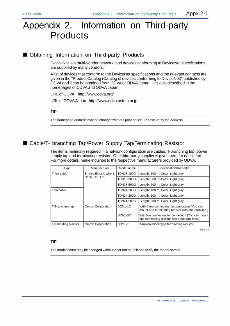
<Toc> <Ind> <Appendix 2. Information on Third-party Products > Appx.2-1
IM 34M6H28-01E
Appendix 2. Information on Third-partyProducts
Obtaining Information on Third-party ProductsDeviceNet is a multi-vendor network, and devices conforming to DeviceNet specificationsare supplied by many vendors.
A list of devices that conform to the DeviceNet specifications and the relevant contacts aregiven in the "Product Catalog (Catalog of devices conforming to DeviceNet)" published byODVA and it can be obtained from ODVA or ODVA Japan. It is also described in thehomepages of ODVA and ODVA Japan.
URL of ODVA http://www.odva.org/
URL of ODVA Japan http://www.odva.astem.or.jp
TIP
The homepage address may be changed without prior notice. Please verify the address.
Cable/T- branching Tap/Power Supply Tap/Terminating ResistorThe items minimally required in a network configuration are cables, T-branching tap, powersupply tap and terminating resistor. One third-party supplier is given here for each item.For more details, make inquiries to the respective manufacturers provided by ODVA.
TA0106.EPS
Type Manufacturer Model name Specification/Remarks
Thick cable Showa Electric wire & Cable Co., Ltd.
TDN18-100G Length: 100 m, Color: Light gray
TDN18-300G Length: 300 m, Color: Light gray
TDN18-500G Length: 500 m, Color: Light gray
Thin cable TDN24-100G Length: 100 m, Color: Light gray
TDN24-300G Length: 300 m, Color: Light gray
TDN24-500G Length: 500 m, Color: Light gray
T-Branching tap Omron Corporation DCN1-1C With three connectors for connection (You can mount one terminating resistor with one drop line.)
DCN1-3C With five connectors for connection (You can mount one terminating resistor with three drop lines.)
Terminating resistor Omron Corporation DRS1-T Terminal block type terminating resistor
TIP
The model name may be changed without prior notice. Please verify the model names.
1st Edition : Feb.01,1999-00

Blank Page

i<Int> <Toc> <Ind>
IM 34M6H28-01E
Revision HistoryEdition
1st
Date
Feb. 1999
Revised Item
New publication
Written by Product Marketing Section, PLC CenterIndustrial Automation Business Head Quarter.Yokogawa Electric Corporation
Published by Yokogawa Electric Corporation2-9-32 Nakacho, Musashino-shi, Tokyo 180-8750, JAPAN
Printed by Yokogawa Graphic Arts Co., Ltd.
1st Edition : Feb.01,1999-00

Blank Page