device packaging - filebox.ece.vt.eduliab/analogue electronics/week 15... · •device packaging...
TRANSCRIPT

Device Packaging
• Device packaging has many important
roles in semiconductor devices
– External circuit connectivity
– Heat removal
• Very important in power applications
– Device protection and support
Presentation
developed by Daniel
Martin and Thomas
LaBelle of FEEC at
Virginia Tech

• Chip packaging should provide good
performance, long lifetime, high reliability
and low cost
– There are many important factors to consider
when designing packaging, each of which can
affect chip performance and usability
• Bonding/wiring/soldering
• Package material
• Shape, size, and type of connectors
• Number, location and type of pins
• Power/current loads
• Parasitic inductances and capacitance
• Heat sinking method and available space

Die Bonding
• Solder
– Single metal
– Alloy
• Eutectic Composition
– Dispensing
• Paste
• Preform
• Deposited directly on
chip during fabrication
• Epoxy
– Electrically conducting
or nonconducting
– Dispensing
• Paste
• Preforms
This is the process of mechanically attaching the semiconductor
chip to the package. It may or may not also create an electrical
connection to the semiconductor chip.
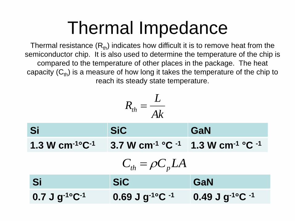
Thermal Impedance
Ak
LRth
Si SiC GaN
1.3 W cm-1°C-1 3.7 W cm-1 °C -1 1.3 W cm-1 °C -1
LACC pth
Si SiC GaN
0.7 J g-1°C-1 0.69 J g-1°C -1 0.49 J g-1°C -1
Thermal resistance (Rth) indicates how difficult it is to remove heat from the
semiconductor chip. It is also used to determine the temperature of the chip is
compared to the temperature of other places in the package. The heat
capacity (Cth) is a measure of how long it takes the temperature of the chip to
reach its steady state temperature.
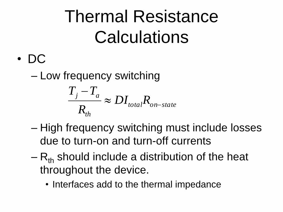
Thermal Resistance
Calculations • DC
– Low frequency switching
– High frequency switching must include losses
due to turn-on and turn-off currents
– Rth should include a distribution of the heat
throughout the device.
• Interfaces add to the thermal impedance
stateontotal
th
ajRDI
R
TT
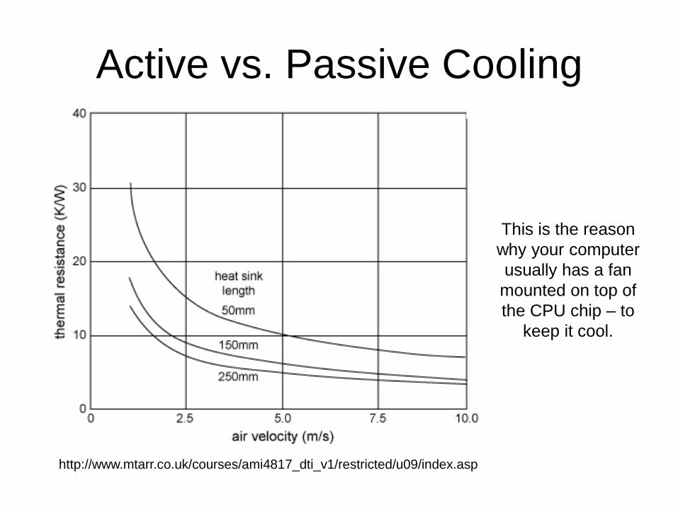
Active vs. Passive Cooling
http://www.mtarr.co.uk/courses/ami4817_dti_v1/restricted/u09/index.asp
This is the reason
why your computer
usually has a fan
mounted on top of
the CPU chip – to
keep it cool.

Wire Bonding
• Bonding makes electrical connections the
device or integrated circuit (IC) to the
outside circuit/circuit board
– There are multiple bonding methods, some for
full chips, others for single devices
• Wire bonding
• Ribbon bonding
• Solder Joint/Bump

Wire Bonding
• Wire bonding is a dominate method due to
several advantages
– Reliable
– Cost-effective
– Flexible/Adaptable to design changes
www.visionxinc.com www.advotech.com
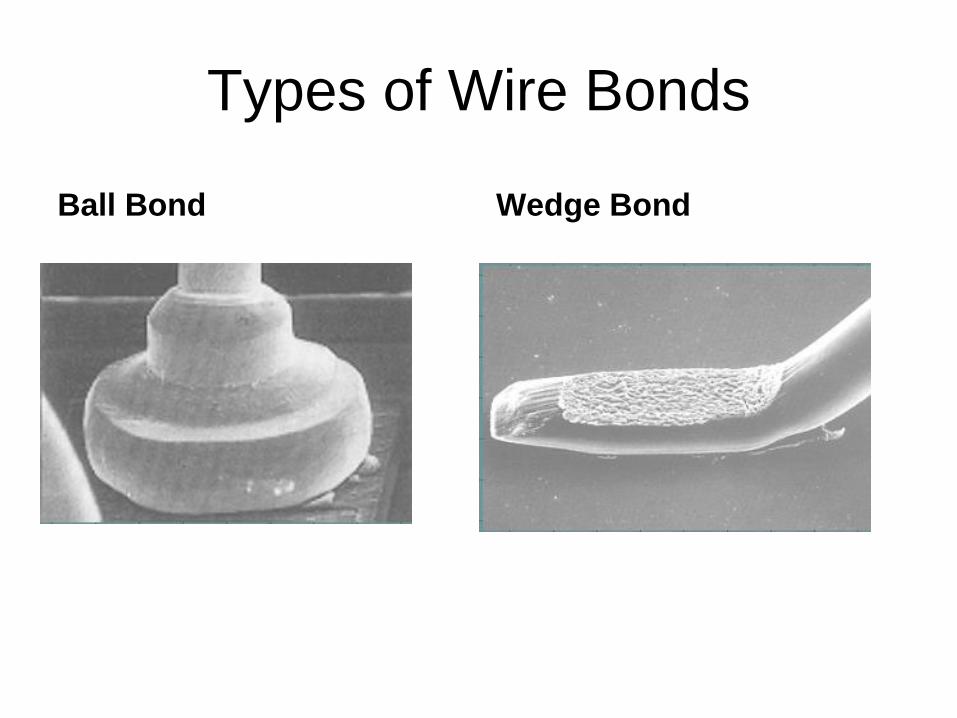
Types of Wire Bonds
Ball Bond Wedge Bond
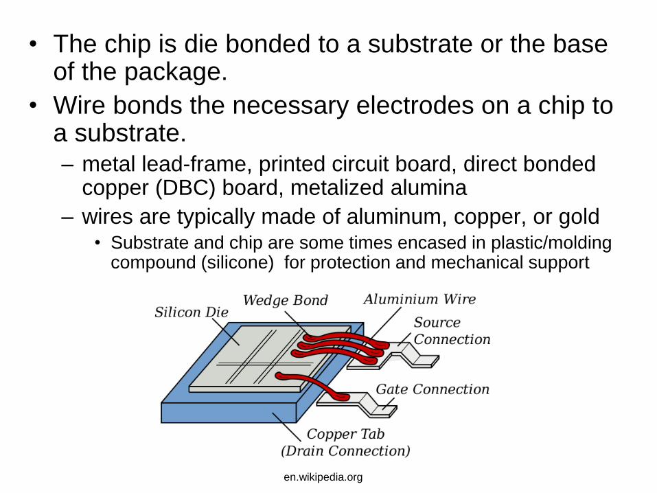
• The chip is die bonded to a substrate or the base of the package.
• Wire bonds the necessary electrodes on a chip to a substrate. – metal lead-frame, printed circuit board, direct bonded
copper (DBC) board, metalized alumina
– wires are typically made of aluminum, copper, or gold • Substrate and chip are some times encased in plastic/molding
compound (silicone) for protection and mechanical support
en.wikipedia.org

• The close packed series of thin wires lead to a
few disadvantages of the wire bond method,
especially for applications involving high power
and/or high frequency
– Electrical and thermal resistance: Wires are very long
and thin. Wires and other parts of the package that
carry current contributed up to 90% of device’s
electrical resistance
– Wires have parasitic inductance, especially at high
frequency
• where L is the parasitic inductance, l is the length of the wire,
d is the diameter of the wire and m is its magnetic
permeability.
– Mechanical bonds introduce a new failure mechanism
)2/(4/1)4log(303.22 lddllL m
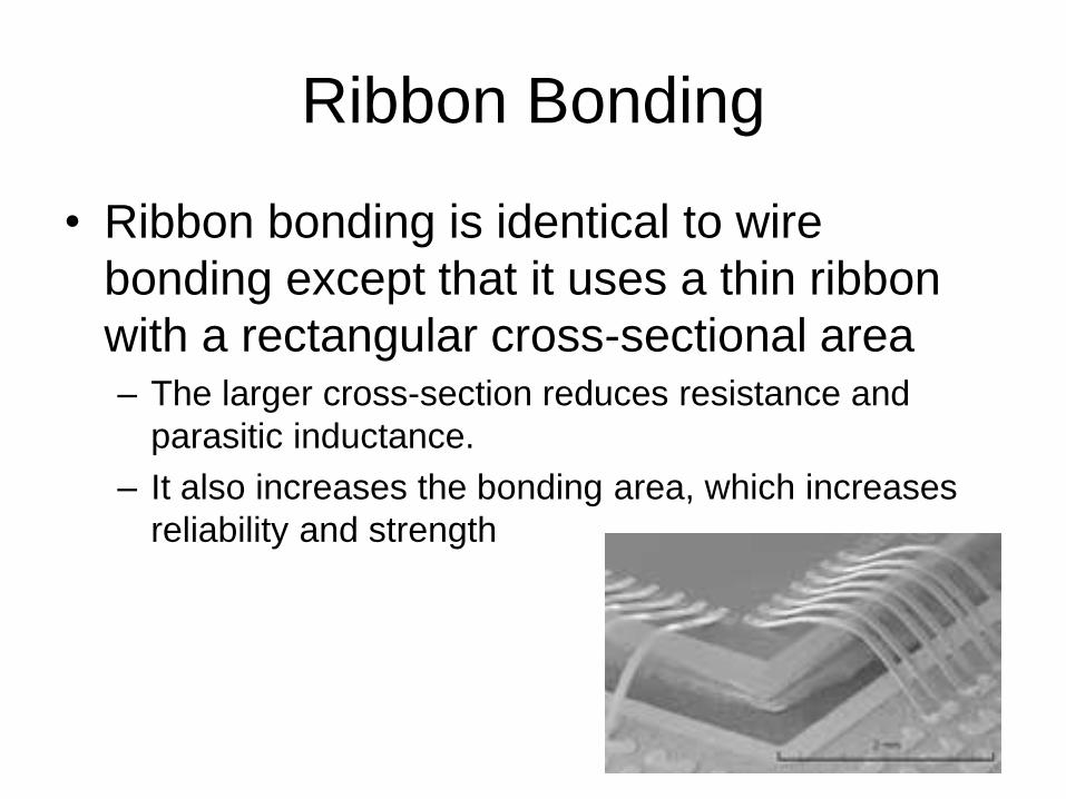
Ribbon Bonding
• Ribbon bonding is identical to wire
bonding except that it uses a thin ribbon
with a rectangular cross-sectional area – The larger cross-section reduces resistance and
parasitic inductance.
– It also increases the bonding area, which increases
reliability and strength
Packaging Research Efforts
• Reduce thermal impedance of the
packaged device/module
• Reduce parasitic inductance
• Reduce cost of packaged device/module
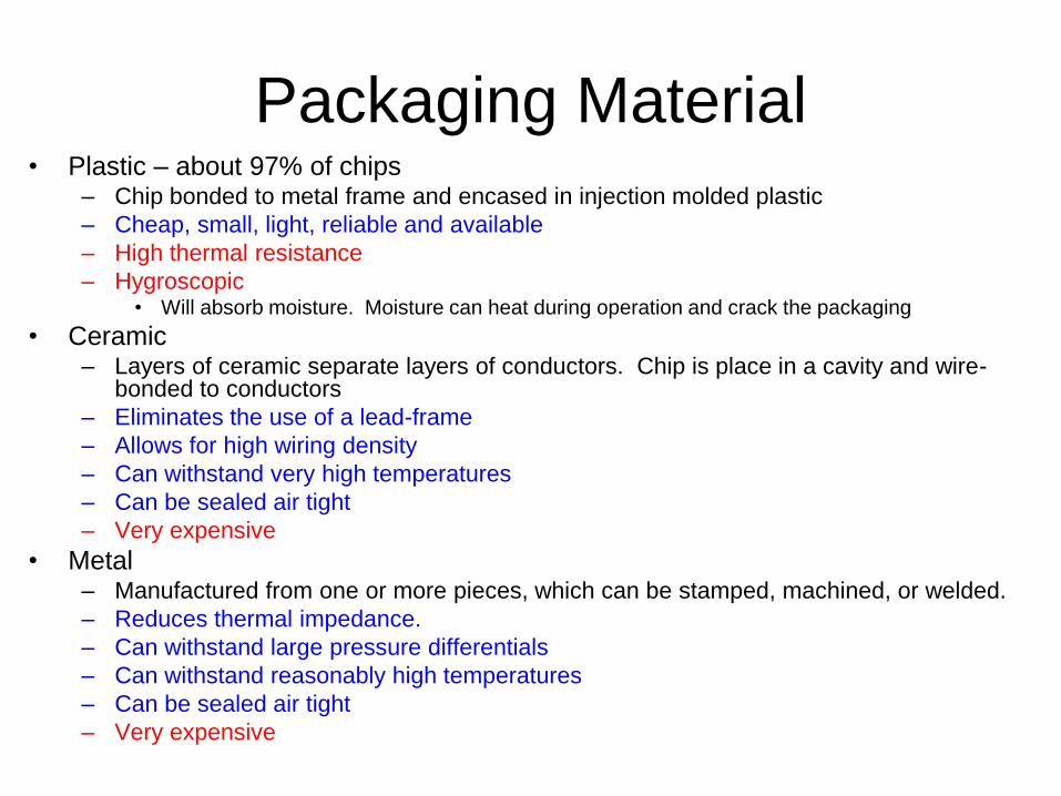
Packaging Material • Plastic – about 97% of chips
– Chip bonded to metal frame and encased in injection molded plastic
– Cheap, small, light, reliable and available
– High thermal resistance
– Hygroscopic • Will absorb moisture. Moisture can heat during operation and crack the packaging
• Ceramic – Layers of ceramic separate layers of conductors. Chip is place in a cavity and wire-
bonded to conductors
– Eliminates the use of a lead-frame
– Allows for high wiring density
– Can withstand very high temperatures
– Can be sealed air tight
– Very expensive
• Metal – Manufactured from one or more pieces, which can be stamped, machined, or welded.
– Reduces thermal impedance.
– Can withstand large pressure differentials
– Can withstand reasonably high temperatures
– Can be sealed air tight
– Very expensive

Mounting
• Semiconductor packages are divided into several mounting schemes. Two common ones are: – Through-hole (left)
• Pins extend from the chip through holes in the board and are soldered on the opposite side
– Surface mounted (right)
• Leads of chip are soldered to matching metallic leads on the top of the board
en.wikipedia.org www.customelectronicsco.com
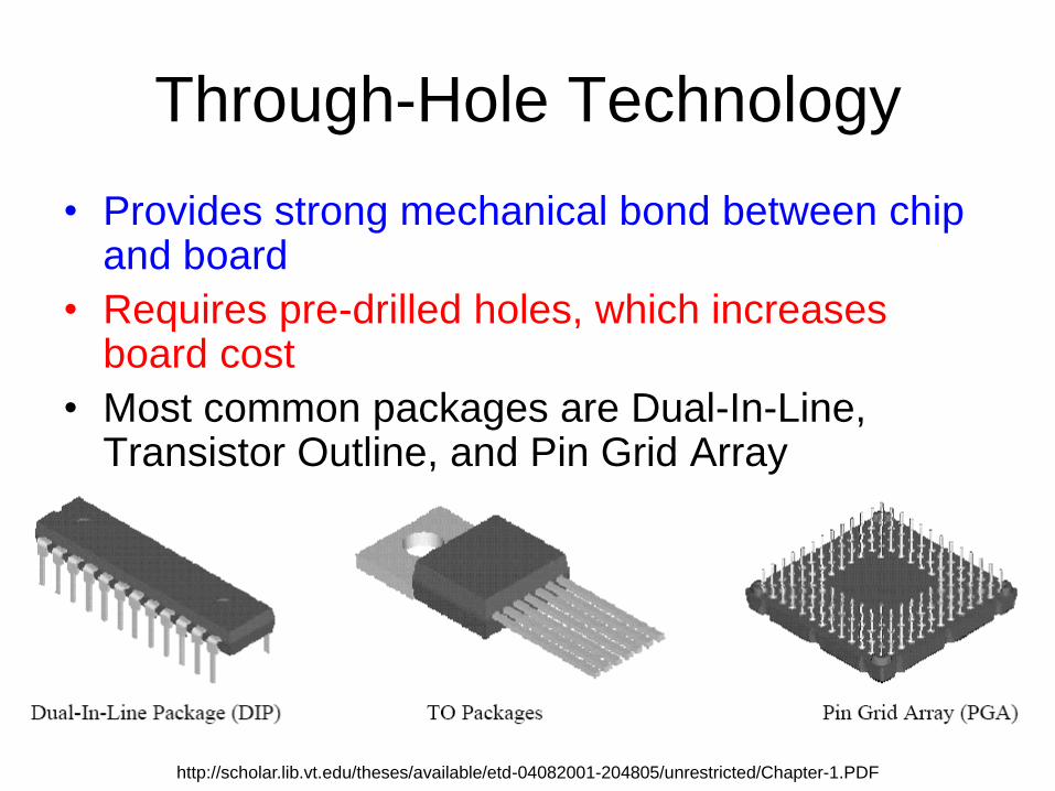
Through-Hole Technology
• Provides strong mechanical bond between chip and board
• Requires pre-drilled holes, which increases board cost
• Most common packages are Dual-In-Line, Transistor Outline, and Pin Grid Array
http://scholar.lib.vt.edu/theses/available/etd-04082001-204805/unrestricted/Chapter-1.PDF
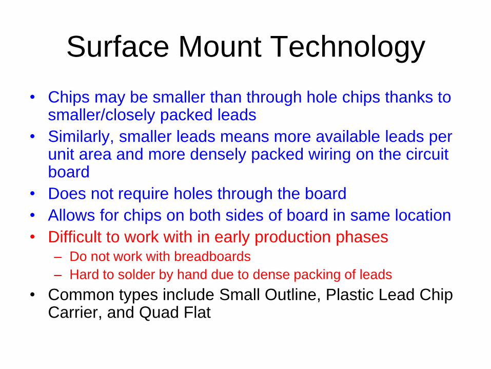
Surface Mount Technology
• Chips may be smaller than through hole chips thanks to smaller/closely packed leads
• Similarly, smaller leads means more available leads per unit area and more densely packed wiring on the circuit board
• Does not require holes through the board
• Allows for chips on both sides of board in same location
• Difficult to work with in early production phases – Do not work with breadboards
– Hard to solder by hand due to dense packing of leads
• Common types include Small Outline, Plastic Lead Chip Carrier, and Quad Flat
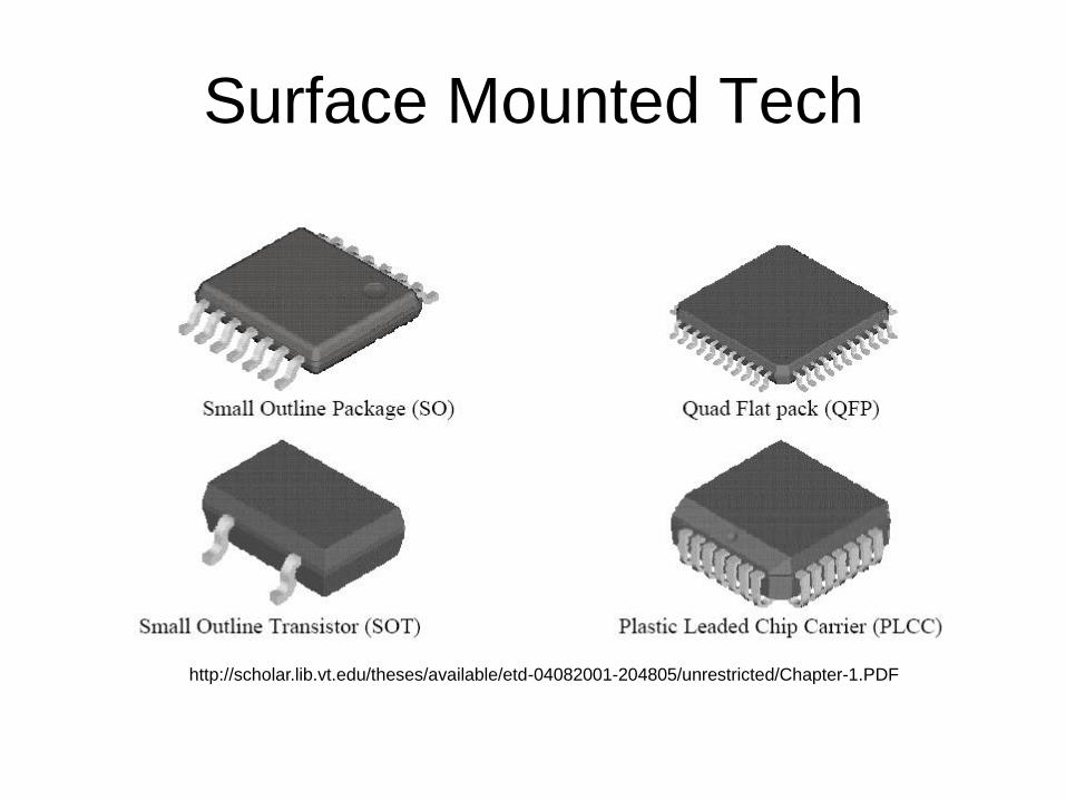
Surface Mounted Tech
http://scholar.lib.vt.edu/theses/available/etd-04082001-204805/unrestricted/Chapter-1.PDF

Ball Grid Array
• The ball grid array is a special high-density surface mount technology, analogous to the pin grid array for TH technology
• In a BGA, balls of solder form a grid pattern on the bottom of the chip or package.
• The chip or package is mounted on the surface of the board and each solder ball corresponds to a metal trace on the board
http://www.flipchips.com/photos/SolderOnNiAu.jpg
• BGA tech allows for very densely packed leads – Ball-to-device proximity allows for short leads, which reduces
resistance and parasitic inductance
• Mounting BGAs on boards can be troublesome because the balls cannot bend to fit the board the way standard leads can – The mechanical integrity of the solder ball joints is also an issue
• In power applications, Fairchild Semiconductor has developed MOSFET BGA packaging in which the MOSFET leads connect directly to a BGA. – This lowers resistance because of the density of ball connections
and the short conductive path
– Heat dispersion is also improved in the same manner
– Fairchild showed that the BGA MOSFET improves on state resistance by 35% and heat dissipation by 175% when compared to the SO-8 chip

Silicon Footprint
• Today, Si processing technology is so advanced that Si
devices are no longer the largest contributor to space
inefficiency. Instead, packaging is now the greatest
issue.
– We use the die-to-footprint ratio as a general measure of
package efficiency. This is simply the ratio of the area of house
Si to the area of the package
– In general, through-hole packages (not including Pin Grid Array)
is very inefficient while surface mount technology, especially
BGA, offers an excellent footprint ratio
Package
SiP
A
AF

Power Electronics
• The operation of packaged power electronics,
which have a large amount of current flowing in
and/or out of them or have very high voltages
applied to their pins are very limited by the
electrical resistance and thermal impedance of
the package.
– Usually, there are very few electrical connections that
need to be made to the semiconductor.
• Efforts have been made to minimize the electrical resistance
of package by using sheets of metal instead of wire or ribbon
bonds and to use materials that conduct heat very well, such
as copper, to reduce the thermal impedance of the package.

Solder Joint • The solder joint method eliminates the use of wires for
bonding the device to the frame – Vishay Siliconiz PowerConnect technology sandwiches the chip
between the bottom and (extended) top lead-frame
• The chip is soldered to the frame. These contact areas are much larger than with wire bonding. – This increase in area leads to better heat performance. The
bonds also do not introduce the long conduction path of that of wire bonding
• Thermal expansion introduces a reliability issue. The chip and the frame do not expand at the same rate, expansion at high temperature operation can lead to mechanical instabilities
Lead-frame
Plastic Casing
Device

• One method that has been introduced in
order to combat the thermal expansion
issue is the inclusion of a layer of
conductive epoxy and the use of a copper
strap
Lead-frame
Plastic Casing
Device
“CopperStrap”
Epoxy
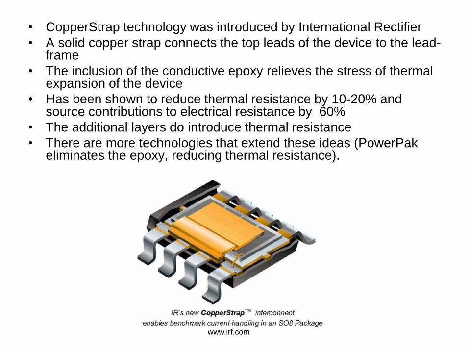
• CopperStrap technology was introduced by International Rectifier
• A solid copper strap connects the top leads of the device to the lead-frame
• The inclusion of the conductive epoxy relieves the stress of thermal expansion of the device
• Has been shown to reduce thermal resistance by 10-20% and source contributions to electrical resistance by 60%
• The additional layers do introduce thermal resistance
• There are more technologies that extend these ideas (PowerPak eliminates the epoxy, reducing thermal resistance).
www.irf.com

DirectFET
• DirectFET is packaging specifically designed (by
International Rectifier) for power MOSFETs
• DirectFET eliminates considerable thermal and
electrical resistance introduced by standard
packaging
powerelectronics.com
DirectFET
• The Si chip is contained within a passivated housing. – The copper is molded to have source and gate on the
bottom in order to make contact to the board.
– A copper “clip” goes over the molding to make the drain connection
• The design eliminates wires, the lead frame and plastic molding – Reduced electrical resistance: 86% less than the
CopperStrap SO-8 chip
– Reduced thermal resistance: from 18-20 C/W in the SO-8 to 1-3 C/W
– Reduced package size