device aging simulations enabling circuit optimizations€¦ · katja puschkarsky 8.11.2017 – mos...
TRANSCRIPT

Katja Puschkarsky 8.11.2017 – MOS AK 13.3.2018
Device aging simulations enabling circuit optimizations
- restricted -

Aging – Critical Stress Conditions?
2 2018-03-13 restricted Copyright © Infineon Technologies AG 2018. All rights reserved.

RESilient Integrated SysTems
› Funded by: BMBF and European Union Catrene Program 01/2015-12/2017
› Motivation:
– Electronic systems in cars planes require high reliability
– New reliability aware design approaches and solutions are needed
– Resist targets: New approaches for resilient integrated systems
Resilience:
– The ability of a system or component to resist a certain load change by adapting its initial stable configuration to the new situation
3 2018-03-13 restricted Copyright © Infineon Technologies AG 2018. All rights reserved.

RESIST Project Partners
4 2018-03-13 restricted Copyright © Infineon Technologies AG 2018. All rights reserved.

Agenda
Worst Case Aging Models
Variability
1
2
3 BTI Recovery
Circuit Simulations 4
Outlook and Cooperation 5
5 2018-03-13 restricted Copyright © Infineon Technologies AG 2018. All rights reserved.

Electrical stress generates charged traps
A. Asenov et. al., Simulation of Instrinsic Parameter Fluctuations in Decananometer and Nanometer-Scale MOSFETs, IEEE Transactions on Electron Devices 50(9), 2003
Tage = 0 a Tage = 1 a Tage = 2 a
charge capture charge emission
D
S
VT = 0.55 V
6 2018-03-13 restricted Copyright © Infineon Technologies AG 2018. All rights reserved.

BTI and HCI Impact on Device Behavior I
NMOS Hot Carrier Injection (HCI) Effect
– Emax at drain corner causes hot carrier generation
– Hot carriers cause Isub, Igate and oxide damages
n+
G D
Ibulk
n+ n+
P-well
Impact Ionization
Ig
Oxide Damage
S
Parametric shift
› Increase of Vth
› Decrease of gm
› Increase of Ioff
› Decrease of Idsat
Degradation f(T,VDS,Vgs)
Doesn’t recover
7 2018-03-13 restricted Copyright © Infineon Technologies AG 2018. All rights reserved.

BTI and HCI Impact on Device Behavior II
Negative Bias Temperature Instability (NBTI) Effect
Positive Bias Temperature Instability (PBTI) Effect
– Hydrogen-silicon bond (Si-H) is broken
– Hydrogen is trapped into the oxide interface trap
n+
G D
p+ p+
n-sub
S
Parametric shift
› Increase of Vth
› Decrease of gm
› Increase of Ioff
› Decrease of Idsat
Degradation f(T,VGS)
Recovers
8 2018-03-13 restricted Copyright © Infineon Technologies AG 2018. All rights reserved.

Worst-Case Aging Models – Main Features 1
BTI - Basic Set of Generic Equations for ∆𝑉𝑡ℎ and ∆𝐼 𝐼𝑜 Contributions
HCI - Basic Set of Generic Equations for ∆𝑉𝑡ℎ and ∆𝐼 𝐼𝑜 Contributions
› ± depends on device type: + for nmos, - for pmos
› 𝑉𝑔𝑠 and 𝑉𝑑𝑠 are time dependent transistor terminal voltages
› Boltzmann term 𝑒𝑥 𝑝 −𝐸𝑎
𝑘𝐵∙𝑇𝑜𝑝 for temperature dependency
› 𝐴 𝑉𝑔𝑠 models the 𝑉𝑔𝑠 dependency by using fit polynomial of low degree (n=6)
› 𝑡𝑜𝑝𝑛 describes extrapolation to final long-term aging time, typically 𝑡𝑜𝑝= 10y
› <…>t is the weighted summation over simulated stress time
› L(…) are limiting functions required for numerical reasons
BTI < L 𝑉𝑔𝑠 ∙ 𝐶 ∙ 𝑒
𝐵𝑉± 𝑉𝑔𝑠
+ −𝐸𝑎
𝑘𝐵∙𝑇𝑜𝑝 +
𝐵𝐿𝐿𝑑𝑒𝑠 >𝑡 ∙ 𝑡𝑜𝑝
𝑛
HCI < L 𝑉𝑔𝑠, 𝑉d𝑠 ∙ 𝐶 ∙ 𝑒
𝐵𝑉± 𝑉𝑑𝑠
+ −𝐸𝑎
𝑘𝐵∙𝑇𝑜𝑝 +
𝐵𝐿𝐿𝑑𝑒𝑠 ∙ 𝐴 𝑉𝑔𝑠 >𝑡 ∙ 𝑡𝑜𝑝
𝑛
9 2018-03-13 restricted Copyright © Infineon Technologies AG 2018. All rights reserved.
Agenda
Worst Case Aging Models
Variability
1
2
3 BTI Recovery
Circuit Simulations 4
Outlook and Cooperations 5
10 2018-03-13 restricted Copyright © Infineon Technologies AG 2018. All rights reserved.

Distribution of the threshold voltage after BTI
6.046.146.296.47
6.576.887.257.78
8.23
-2.5
-2
-1.5
-1
0.5
0
0.5
1
1.5
2
2.5
3
-435 -425 -415 -405 -395 -385 -375 -365
Qu
an
tile
Vth,sat (mV)
virgin
5 sec
18 sec
30 sec
150 sec
656 sec
2801 sec
11890 sec
50393 sec
stress
VG,stress=-2.0V
T=125°C DUT F
100 devices
Standard deviation s (mV):
Schlünder C.; Berthold J.M.; Hoffmann M.; Weigmann J-M.; Gustin W. and Reisinger H.; “A New Smart Device Array Structure
for Statistical Investigations of BTI Degradation and Recovery”, IEEE International Reliability Physics Symposium (IRPS), April
12-14, Monterey, California, 2011, pp. 56-60
Distribution of the threshold voltage after NBTI VG,stress=-2.0V. The variability increases with longer stress times.
Distribution of Vth after NBTI stress
convolution of:
• Distribution of the virgin devices
• Distribution of the NBTI degradation
11 2018-03-13 restricted Copyright © Infineon Technologies AG 2018. All rights reserved.

Impact of BTI Variability
4060nm2 4800nm2 72000nm2 72000nm2 84100nm2 120000nm20
5
10
15
20
25
30
35
40
45
sta
nd
ard
devia
tio
n s
(mV
)
6.8h NBTI
0h
E F DCBA
70nm/58nm
120nm/40nm
120nm/0.6µm
1.45µm/58nm
3µm/40nm 0.6µm/120nm
0 0.005 0.01 0.015 0.020
5
10
15
20
25
sta
nd
ard
devia
tio
n s
(mV
)
1 / sqrt (w l) (1/nm)
sigma of Delta Vth,lin
sigma of Delta Vth,sat
Pelgrom-Plot
NBTI: VGS= -2.0V; T=125°C ; 14h
Schlünder C.; Proebster, F.; Berthold, J.; Gustin, W.; and Reisinger, H.; “Influence of MOSFET geometry on the statistical
distribution of NBTI induced parameter degradation”, Final Report IEEE International Integrated Reliability Workshop (IRW), S.
Lake Tahoe, CA, Oct. 11-15, IRW, pp. 81-86, 2015
Standard deviation s of Vth,lin of the transistors with different areas (nm2) before and after stress
Pelgrom plot of the standard deviations s of the stress induced Vth,lin and Vth,sat shift. Like the s of zero hour parameters also the s of the Vth shift is proportional to ∼1/sqrt(w×l).
12 2018-03-13 restricted Copyright © Infineon Technologies AG 2018. All rights reserved.

Distribution of the threshold voltage after recovery
-2.5
-2
-1.5
-1
0.5
0
0.5
1
1.5
2
2.5
3
-252 -233 -214 -195 -176
Qu
an
tile
Vth,lin (mV)
0.2s2.1s28s594s295 min223.1 h26.1 days67.1 days19 weeks43 weeksvirgin
Recovery
43 weeks recovery
at VG,rec = 0V ; T = 125 C
Technology B
Stress
virgin values
before stress
Schlünder C., Berthold J., Proebster F., Martin A., Gustin W. and Reisinger H.; Degradation and Recovery of variability due to
BTI “, ESREF 2016
Distributions of the threshold voltage after recovery up to 43 weeks at T=125°C. Both the Vth values and the variability recover in direction of the virgin values (rightmost curve).
13 2018-03-13 restricted Copyright © Infineon Technologies AG 2018. All rights reserved.
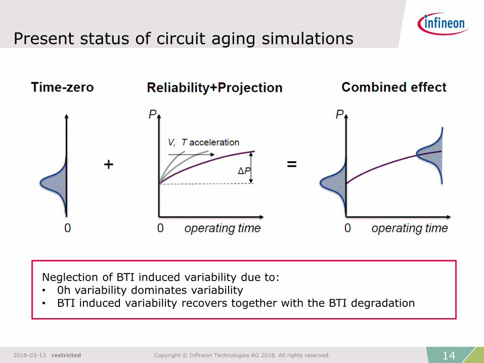
Present status of circuit aging simulations
Neglection of BTI induced variability due to: • 0h variability dominates variability • BTI induced variability recovers together with the BTI degradation
14 2018-03-13 restricted Copyright © Infineon Technologies AG 2018. All rights reserved.

Agenda
Worst Case Aging Models
Variability
1
2
3 BTI Recovery
Circuit Simulations 4
Outlook and Cooperations 5
15 2018-03-13 restricted Copyright © Infineon Technologies AG 2018. All rights reserved.

0 20 40 60 80 1000.0
0.2
0.4
0.6
0.8
1.0
DV
TA
C/ D
VT
DC
PNO 2.2nm / 175 C / Vg=-2.7V
PNO 1.8nm / 85 C / Vg=-2.1V
duty factor (%)
50%
'S-Curve': BTI degradation as a function of the duty-cycle of a rectangular signal (f=100 kHz) applied to the gate for 10ks.
0.00 0.02 0.04 0.06 0.08 0.100.0
0.2
0.4
0.6
0.8
1.0
no
rmalize
d C
harg
e
AC stress time tAC
(s)
ripple
c = 0.5ms
e = 100ms
c = 5ms
e = 5ms
c = 200ms
e = 20ms
A
B
C
Some examples of charging curves of defects with different charging time constants 𝜏 and different ratios 𝜏𝑒 𝜏𝑐
Can we just neglect Recovery of BTI?
Neglecting recovery is more than 2 times over-estimating the degradation after BTI for a duty cycle of 50%
16 2018-03-13 restricted Copyright © Infineon Technologies AG 2018. All rights reserved.

Integrating Recovery into Circuit Simulations
› Why it is so complicated to consider BTI recovery for circuit simulations?
› Recovery depends on the full device history
› real-time simulations necessary
› No simple extrapolation possible
› Physical models: Charging/discharging of every single trap
› Very time-consuming, huge calculation effort
› Simplifications: E.g. Fraunhofer Gesellschaft approach
› But: Still time-consuming and high measurement effort
› New approach developed: Publication will follow soon
17 2018-03-13 restricted Copyright © Infineon Technologies AG 2018. All rights reserved.

Physics-based compact modeling
18 2018-03-13 restricted Copyright © Infineon Technologies AG 2018. All rights reserved.

Agenda
Worst Case Aging Models
Variability
1
2
3 BTI Recovery
Circuit Simulations 4
Outlook and Cooperations 5
19 2018-03-13 restricted Copyright © Infineon Technologies AG 2018. All rights reserved.

Device Aging Simulation – Design Flow
Device Aging Simulation – Design Flow Building Blocks Multi-step Spice simulation sequence
1. Fresh Simulation
2. Stress Simulation
3. Aged Simulation
deploying
– A Spice simulation engine
– Add-on worst-case aging models
– assertions for stress integration
– alter concept for instance specific
– Avenue/ADE-XL test sequence as flow control engines
20 2018-03-13 restricted Copyright © Infineon Technologies AG 2018. All rights reserved.

Worst-Case/Realistic Stress Conditions
Main Impact Factors
• Aging Model Dependencies (VDS, VGS, Temperature)
• Analog Circuit Modes (Circuit Duty Cycles, Sleep Modes, Start-up Phase)
Temperature Implications
• local temperature increase
• mixed temperature stress profiles
• worst-case temperature condition for single device dependent on aging effect (BTI, HCI) and device type, but circuit contains always a mixture
Stress Scenario Discussion
• worst-case vs. realistic stress pattern
• suppression of start-up simulation phases
• handling of complex multi-circuit mode stress pattern
21 2018-03-13 restricted Copyright © Infineon Technologies AG 2018. All rights reserved.

Comparison IV, NOR
BTI
HCS
For the NOR ringo, HCS should play a less dominant role, than for the IV due to the exponential drain voltage dependence
22 2018-03-13 restricted Copyright © Infineon Technologies AG 2018. All rights reserved.

Results: Inverter Ringo, T=175°C, Vdd=2.4V
Frequency recorded during stress
HCS and BTI contribute both approx. equally
23 2018-03-13 restricted Copyright © Infineon Technologies AG 2018. All rights reserved.

Outlook & cooperation
› Efficient usable worst case models were developed
› Variability is currently neglected (0h hour variability has been shown to be bigger than aging-induced variability)
› Recovery is no longer neglected – Publication will follow soon
› Relevant circuit examples (Ring- and Relaxation-Oscillators) are further studied
24 2018-03-13 restricted Copyright © Infineon Technologies AG 2018. All rights reserved.
