development of the large-area picosecond...
TRANSCRIPT

Development of the
Large-Area Picosecond
Photo-Detectors
Andrey ElaginUniversity of Chicago
3rd Berkeley Workshop on the Direct Detection of Dark MatterLBL, December 6, 2016

Outline
• LAPPD Overview
• Commercialization status at Incom Inc.
• R&D Towards Volume Production
- development of in-situ assembly process at UChicago
- Gen-II LAPPD
2

LAPPD
3
Micro-Capillary Arrays by Incom Inc.
Material: borofloat glass Area: 8x8” Thickness: 1.2mm Pore size: 20 mm
Open area: 60-80%
Atomic Layer Deposition (ALD)- J.Elam and A.Mane at Argonne
(process is now licensed to Incom Inc.)- Arradiance Inc. (independent process)
Micro-Channel Plates (MCPs)
20x20 cm2
~15mm
Large-Area Picosecond Photo-Detector
1.2mm

4
LAPPD Electronics
Delay-line anode
- 1.6 GHz bandwidth
- number of channels
scales linearly with area
PSEC-4 ASIC chip
- 6-channel, 1.5 GHz, 10-15 GS/s
30-Channel ACDC Card (5 PSEC-4) Central Card
(4-ACDC;120ch) 4
NIM 711 (2013) 124
NIM 735 (2014) 452

LAPPD Prototype Testing ResultsSingle PE resolution
RSI 84, 061301 (2013), NIMA 732, (2013) 392
NIMA 795, (2015) 1See arXiv:1603.01843
for a complete LAPPD bibliography
Demonstrated characteristics:single PE timing ~50psmulti PE timing ~35 ps
differential timing ~5 psposition resolution < 1 mm
gain >107
Reconstruction of the laser beam footprint
5

LAPPD Sealing Attempt @ SSL Berkeley
2014 JINST 9 C04002
A fully processed ceramic LAPPD tile was tested while still in the vacuum chamber• Peak QE ~25%• QE non-uniformity +/-15% over 20x20 cm2 area• No change in QE after 2 weeks• TTS ~ 200 ps (FWHM, using 80ps laser and
ad-hoc connectors to get signal out of the vacuumchamber)
6
QE uniformity map

Commercialization Status
7
• April 2014 - DOE funding to create infrastructure and demonstrate a pathway towards pilot production
• November 2015 – Facility operational• December 2015 – Commissioning trial initiated• October 2016 – First Sealed Tile with Bialkali Photocathode• Now transitioning from “commissioning” to “exploitation” stage

LAPPDTM @ Incom Inc.
Slide courtesy of Incom Inc. 8

Goal of the R&D Effort at UChicagoAffordable large-area many-pixel photo-detector systems
with picosecond time resolution
LAPPD module 20x20 cm2 Example of a Super Module
9UChicago goal is to enable high volume production
at Incom so we can do physics using LAPPDTM
A production rate of 50 LAPPDs/week
would cover 100m2 in one year• High volume production can be challenging• We are exploring if a non-vacuum transfer process
can be inexpensive and easier for a very high volume production

In-Situ Assembly StrategySimplify the assembly process by avoiding vacuum transfer:
make photo-cathode after the top seal(PMT-like batch production)
Step 1: pre-deposit Sb on the top window prior to assemblyStep 2: pre-assemble MCP stack in the tile-baseStep 3: do top seal and bake in the same heat cycle
using dual vacuum systemStep 4: bring alkali vapors inside the tile to make photo-cathodeStep 5: flame seal the glass tube or crimp the copper tube
UChicago processing chamber
10

In-Situ Assembly Facility UChicago
Looking forward towards transferring the in-situ process to industry
The idea is to achieve volume production by operating many small-sizevacuum processing chambers at the same time
UChicago PSEC Lab
11
Heat only the tilenot the vacuum vessel
Intended for parallelization

First Signals from an In-Situ LAPPD
Near side: reflection from unterminated far end
Far side: reflection is superimposed on prompt
Source
far sidenear side
Source
Readout(50-Ohm transmission line)
(Sb cathode)
Readout(50-Ohm transmission line)
12The tile is accessible for QC before photo-cathode shot
Could help the production yield
April, 2016

Sb layer only Cs-Sb photo-cathode
1st In-Situ Photo-Cathode
Cs
Relative QE measurementFirst in-situ commissioning run- saw first photo-current response from
in-situ photo-cathode- measured relative QE (absolute QE is tricky
due to DC current through the whole stack)- demonstrated a sealed tile configuration
- no QE drop for 2 weeks after the valve to the pump was closed
- no QE drop for 3 weeks after flame seal
Note on this commissioning run:PC is very thick for transmission mode operation
(initial 20nm of Sb translates into ~80nm of Cs-Sb) 13
near center
far
July, 2016
Absolute QE > 0.01%

Flame SealAugust 18, 2016
14
Flame seal by J.Gregar, Argonne

2nd In-Situ Photo-Cathode
• Thinner Sb layer (~10nm)• Improved instrumentation
and process control• A factor of 10 improvement in QE• Currently doing life-time testing
(flame sealed on Nov 16)
Oct - Nov, 2016 UChicago PSEC Lab
15
Absolute QE > 0.1%

Gen-II LAPPD
16
10 nm NiCr ground layer insideis capacitively coupled
to an outside 50 Ohm RF anode
NiCr-Cu electrodingfor the top seal
Ground pins
Two tubulation portsfor the in-situ PC synthesis
(improved gas flow)
Monolithic ceramic body
• Robust ceramic body• Fused silica window• Anode is not a part of
the vacuum package• Enables fabrication
of a generic tile fordifferent applications
• Compatible with in-situ and vacuum transfer assembly processes
Joint effort with Incom Inc. via DOE NP SBIR Phase-I
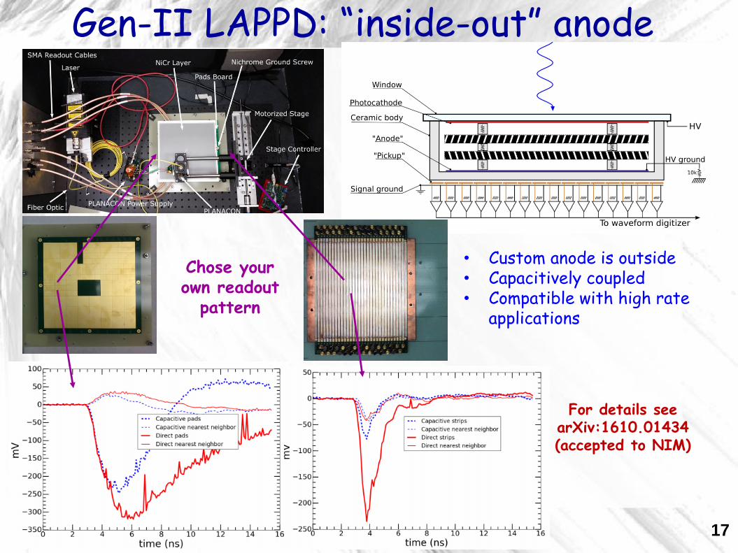
Gen-II LAPPD: “inside-out” anode
• Custom anode is outside• Capacitively coupled • Compatible with high rate
applications
For details see arXiv:1610.01434(accepted to NIM)
17
Chose yourown readout
pattern

Gen-II LAPPD: work in progress
18
December, 2016

Summary
• Commercialization at Incom Inc. goes well
- recently demonstrated first sealed functional LAPPD with
bi-alkali photo-cathode
- transitioning from “commissioning” to “exploitation” stage
• With the goal to use LAPPDs in large experiments
UChicago group is focused on R&D for high volume
production process
• Making photo-cathode in-situ as a final step is very attractive
- leak check before PC-synthesis
- real-time tuning and optimization of PC is possible
• Right at the moment UC group is working on photo-cathode
optimization and Gen-II LAPPD vacuum packaging
- moving towards K2CsSb photo-cathode trials
- building 2nd vacuum processing chamber -> parallelization
19

Back-up

Early Adopters of LAPPD
Some examples of early adopters:
• ANNIE – Accelerator Neutrino Neutron Interactions Experiment• Cherenkov/Scintillation light separation for particle ID• Optical Time Projection Chamber• TOF measurements at Fermilab Test Beam• There are many more (lots of interest shown at the “Early Adopters
Meeting” hosted by Incom Inc. in 2013)
9
Putting first LAPPD tiles into real experimental settings for testingis the highest priority

22
Slide credit: Henry Frisch
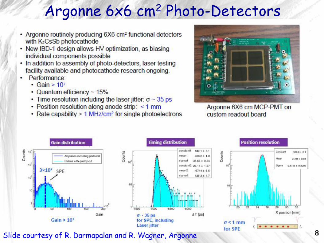
Slide courtesy of R. Darmapalan and R. Wagner, Argonne
Argonne 6x6 cm2 Photo-Detectors
8

Can you make PC after Sb was exposed to air?
Luca Cultrera at Cornell

What about noise in the MCPs after Cs-ation?
Matt Wetstein


In-Situ Process Pre-requisiteReliable hermetic seal over a 90-cm long perimeter
Indium Solder Flat Seal RecipeInput:
• Two glass parts with flat contact surfaces
Process:
• Coat 200 nm of NiCr and 200 nm of Cu
on each contact surface (adapted from
seals by O.Siegmund at SSL UC Berkeley)
• Make a sandwich with indium wire
• Bake in vacuum at 250-300C for 24hrs
Key features:
• A good compression over the entire perimeter
is needed to compensate for non-flatness and
to ensure a good contact
• In good seals indium penetrates through entire
NiCr layer (Cu always “dissolves”)
glass window(8.66x8.66”)
glass frame(sidewall)
Sealed LAPPD tile
This recipe is now understood
It works well over large perimeters16Metallization and compression are critical

Indium seal recipes exist for a long time
PLANACONTM
(MCP-PMT by Photonis)
5 cm
Make larger photo-detectors
Our recipe scales well to large perimeter
Simplify the assembly process
Our recipe is compatible with PMT-like batch
production
Why do we need another indium seal recipe?
We adapted NiCr-Cu scheme
from O.Siegmund at SSL UC Berkeley

Metallurgy of the SealModerate temperatures and short exposure time:
• A thin layer of copper quickly dissolves in molten indium
• Indium diffuses into the NiCr layer
Depth profile XPS
The ion etch number is a measure for the depth of each XPS run
Layer depth (uncalibrated)
XPS access courtesy ofJ. Kurley and A. Filatov at UChicago
Glass with NiCr-Cu metallization exposed to InBi at ~100C for <1hrs
(it seals at these conditions)
InBi was scraped when still above melting (72C)
Low melting InBi alloy allows to explore temperaturesbelow melting of pure In (157C)

Metallurgy of the Seal
SEM and EDAX of the metal surfacescraped at the interface
SEM/EDAX data courtesy of J. Elam at Argonne
Glass with NiCr-Cu metallization bonded by pure In at ~250C for 2hrs
(it seals at these conditions)
Cut and scrape at the metal-glass interface
In:77-86%
Ni: 4-12%
Cu: 1-6%
High temperatures and long exposure time
• Indium penetrates through entire NiCr layer
Cr: 1-16%
glass window
sidewall
indium seal

Metallurgy of a Good SealHigher temperatures and longer exposure time
• Indium penetrates through entire NiCr layer
XPS of the glass side of the interface
XPS data courtesy of A. Filatov at UChicago
Cut and scrape at the metal-glass interface
Inte
ns
ity (
a.u
.)
900 800 700 600
Ni(2p)Cr(2p)
control surface
scraped region
In(3p)
Binding energy, eV
Glass with NiCr-Cu metallization bonded by pure In at ~350C for 24hrs
(it seals at these conditions)
We now reliably seal at 250-300C for 12-24hrs