development of efficient permeation barriers based on hot
TRANSCRIPT
HAL Id: pastel-01067937https://pastel.archives-ouvertes.fr/pastel-01067937
Submitted on 24 Sep 2014
HAL is a multi-disciplinary open accessarchive for the deposit and dissemination of sci-entific research documents, whether they are pub-lished or not. The documents may come fromteaching and research institutions in France orabroad, or from public or private research centers.
L’archive ouverte pluridisciplinaire HAL, estdestinée au dépôt et à la diffusion de documentsscientifiques de niveau recherche, publiés ou non,émanant des établissements d’enseignement et derecherche français ou étrangers, des laboratoirespublics ou privés.
Development of efficient permeation barriers based onhot-wire CVD grown silicon-nitride multilayers for
organic devices deposited on flexible substratesSubimal Majee
To cite this version:Subimal Majee. Development of efficient permeation barriers based on hot-wire CVD grown silicon-nitride multilayers for organic devices deposited on flexible substrates. Materials Science [cond-mat.mtrl-sci]. Ecole Polytechnique X, 2014. English. pastel-01067937

THÈSE
Présentée en vue d’obtenir le grade de
DOCTEUR DE L’ÉCOLE POLYTECHNIQUE
Spécialité “Physique et Science des Matériauxˮ
par
SUBIMAL MAJEE
DEVELOPMENT OF EFFICIENT PERMEATION
BARRIERS BASED ON HOT-WIRE CVD GROWN
SILICON-NITRIDE MULTILAYERS FOR ORGANIC
DEVICES DEPOSITED ON FLEXIBLE SUBSTRATES
Thèse soutenue le 10 Septembre 2014 devant le jury compose de :
Prof. Laurence VIGNAU Institut Polytechnique de Bordeaux Reviewer
Prof. Dr. Ruud SCHROPP Eindhoven University of Technology Reviewer
Dr. Alain MADEC Air Liquide Examiner
Prof. Pedro ALPUIM INL, Portugal Examiner (President)
Prof. Yvan BONNASSIEUX Ecole Polytechnique Director of thesis
Dr. Jean-Eric BOURÉE Ecole Polytechnique Invited

ii
Summary in English
Efficient gas-diffusion (permeation) barriers are needed for organic optoelectronic devices because the
presence of moisture or oxygen can cause strong degradation. In order for these devices to operate
continuously during a long term, so to be commercialized, a reliable flexible thin film encapsulation is
required, which is a major challenge. Very low water vapor transmission rates of the order of 10-5
g/m2.day are
required. To reach this goal two ways have been adopted: on one hand fabricating SiNx:H / SiNx:H multilayer
barriers separated by a specific Ar plasma treatment, on the other hand fabricating the conventional
inorganic/organic hybrid multilayer moisture barriers.
We have chosen hot-wire chemical vapor deposition (HW-CVD) as the main technique for depositing the
inorganic layers and a large part of our efforts has been devoted to the complete study of the parameters
controlling the plasma treatment: the energy of the ions impinging the inorganic surfaces was crucial. Several
analytical (morphological, structural, optical, electrical) techniques have been necessary to assess qualitatively
and quantitatively the different layers composing the moisture barriers. A physical interpretation of the plasma
process treatment has been given, based on the interface atomic rearrangements induced by the low energy
ions (< 40 eV). For each way of encapsulation, we have obtained very low water vapor transmission rates (4
to 7 × 10⁻⁵
g/m2.day). Combining above two encapsulation methods, we have achieved extremely low WVTR
rate (6 × 10⁻⁶
g/m2.day), which seems sufficient for the utilization of organic electronic devices.
Résumé en français
Les dispositifs optoélectroniques à base de matériaux organiques nécessitent la réalisation de couches barrière
de perméation car l’oxygène et l’humidité dégradent fortement ces dispositifs. Afin d’augmenter leur durée de
vie et ainsi les rendre commercialement attractifs, des couches d’encapsulation sont nécessaires, ceci
représente un défi majeur surtout dans le cadre des substrats flexibles comme les plastiques. Des faibles
valeurs du taux de perméation sont exigées, typiquement de l’ordre de 10-5
g/m2.jour dans le cadre de l’eau.
Deux voies ont été étudiées, dans le cadre de cette thèse, pour atteindre cet objectif: d’une part en fabriquant
des barrières multicouches à base de nitrure de silicium amorphe, chaque couche étant séparée de la suivante
par un traitement plasma d’argon, d’autre part en fabriquant des barrières hybrides alternant des couches
inorganiques avec des couches organiques.
Nous avons choisi la technique de dépôt chimique en phase vapeur par filament chaud (HW-CVD) pour le
dépôt des couches inorganiques et nos efforts ont porté sur l’étude approfondie des paramètres contrôlant le
plasma. Il ressort que l’énergie des ions impactant la surface a été le paramètre déterminant. Diverses
techniques d’analyse ont été nécessaires pour évaluer précisément la qualité des couches constituant les
barrières de perméation. Une interprétation physique du procédé plasma a été proposée, basée sur le
réarrangement atomique induit à chaque interface par les ions de faible énergie (< 40 eV). Pour chacune des
voies choisies, des très faibles taux de perméation (4 à 7 × 10⁻⁵
g/m2.jour) ont été atteints. Avec la
combinaison de ces deux méthodes d'encapsulation, nous avons atteint une valeur de WVTR extrêmement
faible (6 × 10⁻⁶
g/m2.jour), ce qui semble suffisant pour l’utilisation dans des dispositifs organiques.
iii
ACKNOWLEDGEMENTS
Most of all, I would like to acknowledge Prof. Yvan Bonnassieux for accepting me as a graduate doctorate
student and providing me an opportunity to work in his OLAE group. It is quite impossible for me to imagine
such an encouraging, friendly, motivating and enthusiastic PhD supervisor. I thank him from my heart for all
his support throughout this thesis work and giving me freedom to work with my own ideas. I also
acknowledge his financial support for giving me many chances to attend both national and international
meetings and conferences to present our scientific results.
I am thankful to our laboratory director Dr. Pere Roca i Cabarrocas for creating a wonderful working
atmosphere inside the lab. I would also like to acknowledge the scientific discussions with him. I thank our
former director Dr. Bernard Drévillon for his administrative help during the initial stages of my thesis.
I am honored to have had a very distinguished jury composed of Prof. Laurence VIGNAU, Prof. Dr. Ruud
SCHROPP, Dr. Alain MADEC, Prof. Pedro ALPUIM, Prof. Yvan Bonnassieux and Dr. Jean-Eric Bourée. I
would like to thank them all for their presence at my thesis defense.
I take the opportunity to thank Dr. Jean-Eric Bourée for his precious guidance and support throughout this
work. I was fortunate enough for having such a co-supervisor in my thesis. Being always motivating and
enthusiastic, he encouraged me throughout this thesis work. I would like to acknowledge his initial support for
giving me the chance to start the PhD work under the PICS (French-Portuguese no: 5336) project framework.
His scientific ideas and discussions forced me to think deeply and thoroughly to complete this work. Thank
you for your patience!
My deepest gratitude to Dr. Bernard Geffroy for all his involvement from the beginning in this work and
valuable guidance. His scientific comments and suggestions throughout this thesis work helped me to
complete this work successfully.
I acknowledge the technical and scientific supports from Dr. Denis Tondelier and Dr. Jean-Charles Vanel.
Their help in the implementation of the permeation measurement system and other characterizations reduced
the wastage of time which was a major advantage in completing the thesis on time.
Nothing would be possible without the enormous supports and helps from our Portugal team! Thank you Prof.
Pedro Alpuim and Prof. Fatima Cerqueira. Your huge effort in fabricating lots of samples during this whole
thesis is really praiseworthy. I take this opportunity to thank you both for being always optimistic in this
research and your excellent thinking in the optimization of lots of experimental parameters. I also
acknowledge your cordial support during my nice stay in Braga for two months. It was an excellent
opportunity for me to visit INL.

iv
Thanks to the technical, IT and administrative teams of the lab, who always made it possible to work without
any difficulties. I would like to thank Cyril Jadaud, Jean-Luc Moncel, Frédéric Farci, Jérome Charliac, Eric
Paillassa, Frédéric Liège, Laurence Corbel, Chantal Geneste and Carine Roger-Roulling.
I would like to acknowledge the persons who helped me in different characterization techniques: Enric Garcia
Caurel, Martin Foldyna, Bicher Haj Ibrahim, Jacqueline Tran, Hassina D. Habak, Jean-François Besnier
(TOTAL), Robert Cortes (PMC), Isabelle Maurin (PMC), Fouad Maroun (PMC), Patrick Chapon (Horiba),
Jocelyne Leroy (CEA). It was a nice opportunity to work either directly or indirectly with those persons. It
was an excellent chance to discuss our ideas with Marc Chatelet, Holger Vach, Jean-Luc Maurice and Erik
Johnson. I thank them all.
I wish to thank Pavel Bulkin for his useful scientific comments and suggestions in this thesis. I acknowledge
his help in fabricating numerous numbers of samples grown by MDECR for me.
I would like to thank all my colleagues and friends: Saumyadeep Misra, Chang Hyun Kim, Sungyeop Jung,
Jinwoo Choi, Taewoo Jeon, Xiaoguang Huang, Thamer Ma, David Brunel, Fulvio Michelis, Anna
Shirinskaya, Heejae Lee, Gijun Seo, Hadouchi Warda, Tapajyoti Das Gupta, Supratik Banerjee, Indranil
Dutta, Syam Sundar De, Marc Chaigneau, Gilles Horowitz, Gaël Zucchi, Abderrahim Yassar, Bérengère
Lebental, Stanislas Deby, Sofia Gaiaschi, Anirban Dhar, Mallesham Godumala, Prabal Goyal, Huda Haddad,
Fatme Jardali, Lucie Leveau, Appan Masillamani, Razvigor Ossikovski, Angelo Pierangelo, Leandro Sacco,
Alienor Togonal, Miguel Angel Torres Miranda, Ileana Florea, Fatima Zahra Bouanis.
I appreciate the financial support from Direction des Relations Extérieures (DRE), Ecole Polytechnique during
this thesis. I would like to thank Sylvain Ferrari (DRE), Cecile Vigouroux (DRE), Pascale Fuseau (DRE),
Elisabeth Crepon (DRE), Thanh-Tâm Lê (Graduate School), Audrey Lemarechal (Graduate School), Fabrice
Baronnet (Graduate School) and Christine Ferret (Graduate School).
I wish to acknowledge the initial support from Thierry Gacoin (PMC), Jacques Peretti (PMC) and Yves
Lassailly (PMC) during the first year in Ecole Polytechnique.
I would like to thank my former professors at the University of Calcutta, India. I am grateful to Prof. P. K.
Basu and Prof. Susanta Sen for their huge support to continue the exchange master program with Ecole
Polytechnique.
Finally, I wish to express my deep appreciation to my parents, my wife, my brother and my extended family
members for their moral support, endless love and continuous encouragement.

v
CONTENTS
Page
CONTENTS ------------------------------------------------------------------------------------------------ v
LIST OF TABLES ----------------------------------------------------------------------------------------- ix
LIST OF FIGURES --------------------------------------------------------------------------------------- x
NOMENCLATURE --------------------------------------------------------------------------------------- xvi
1. INTRODUCTION ---------------------------------------------------------------------------------- 1
1.1 ORGANIC OPTO-ELECTRONIC DEVICES ---------------------------------------------- 1
1.2 CHALLENGES OF ORGANIC OPTO-ELECTRONIC DEVICES --------------------- 3
1.2.1 Encapsulation barrier ---------------------------------------------------------------------- 4
1.2.2 Flexible substrate --------------------------------------------------------------------------- 6
1.3 MEASUREMENT OF PERMEATION RATES -------------------------------------------- 7
1.4 ENCAPSULATION BARRIER TECHNOLOGY ------------------------------------------ 7
1.4.1 Single-layer thin film barrier ------------------------------------------------------------- 8
1.4.2 Multilayer thin film encapsulation ------------------------------------------------------- 10
1.5 OBJECTIVE AND ORGANIZATION OF DISSERTATION ---------------------------- 12
2. EXPERIMENTAL TECHNIQUES -------------------------------------------------------------- 14
2.1 BARRIER FILM DEPOSITION SYSTEMS ------------------------------------------------ 14
2.1.1 Twin chamber CVD system -------------------------------------------------------------- 14
2.1.1.1 HW-CVD chamber -------------------------------------------------------------- 15
2.1.1.2 RF PE-CVD chamber ------------------------------------------------------------ 17
2.1.2 Matrix Distributed Electron Cyclotron Resonance PECVD (MDECR-PECVD) - 18
2.1.3 Spin coating --------------------------------------------------------------------------------- 20
2.2 MORPHOLOGICAL CHARACTERIZATION --------------------------------------------- 21
2.2.1 Profilometry -------------------------------------------------------------------------------- 21
2.2.2 Atomic force microscopy (AFM) -------------------------------------------------------- 21
2.3 STRUCTURAL CHARACTERIZATION --------------------------------------------------- 22
2.3.1 X-ray diffraction (XRD) ------------------------------------------------------------------ 22
2.3.2 X-ray reflectometry (XRR) --------------------------------------------------------------- 22
2.3.3 X-ray photoelectron spectroscopy (XPS) ----------------------------------------------- 24
2.3.4 Glow discharge optical emission spectroscopy (GD-OES) -------------------------- 24
2.3.5 Fourier transform infrared spectroscopy ------------------------------------------------ 25
2.4 OPTICAL CHARACTERIZATION ---------------------------------------------------------- 26
2.4.1 UV-visible spectroscopic ellipsometry (UV-visible SE) ----------------------------- 26
2.4.2 Integrating sphere -------------------------------------------------------------------------- 27

vi
2.5 PERMEATION BARRIER CHARACTERIZATION -------------------------------------- 27
2.5.1 Calcium corrosion method ---------------------------------------------------------------- 29
2.5.2 Experimental method ---------------------------------------------------------------------- 30
2.5.3 Calculations --------------------------------------------------------------------------------- 31
2.5.4 Calibration ---------------------------------------------------------------------------------- 34
2.5.5 Result computation ------------------------------------------------------------------------ 35
2.5.6 Method sensitivity and reproducibility -------------------------------------------------- 37
2.5.7 Technical drawbacks ---------------------------------------------------------------------- 37
2.6 MECHANICAL CHARACTERIZATION --------------------------------------------------- 38
2.7 SUMMARY OF CHAPTER 2 ----------------------------------------------------------------- 40
3. PROPERTIES OF HW-CVD GROWN SILICON NITRIDE FILMS ------------------- 41
3.1 INTRODUCTION ------------------------------------------------------------------------------- 41
3.2 HW-CVD PARAMETERS AND DEPOSITION CONDITIONS ------------------------ 42
3.2.1 Choice of filament material --------------------------------------------------------------- 42
3.2.2 Filament temperature (Tf) ----------------------------------------------------------------- 42
3.2.3 Filament to substrate distance (df-s) ------------------------------------------------------ 43
3.2.4 Substrate temperature (Ts) ---------------------------------------------------------------- 43
3.2.5 Working gas pressure (pg) ---------------------------------------------------------------- 44
3.2.6 Source gases -------------------------------------------------------------------------------- 44
3.3 GROWTH MECHANISMS -------------------------------------------------------------------- 45
3.3.1 Dissociation of source gases -------------------------------------------------------------- 45
3.3.2 Gas phase reactions ------------------------------------------------------------------------ 47
3.3.3 Surface reactions --------------------------------------------------------------------------- 48
3.4 DEPOSITION AND OPTIMIZATION OF FILM GROWTH ---------------------------- 48
3.5 CHARACTERISTICS OF OPTIMIZED SiNx:H SINGLE-LAYER FILMS ------------ 52
3.5.1 Optical characteristics --------------------------------------------------------------------- 52
3.5.2 Structural characteristics ------------------------------------------------------------------ 54
3.5.3 Morphological characteristics ------------------------------------------------------------ 55
3.5.4 Barrier characteristics of single-layer films -------------------------------------------- 58
3.6 MULTILAYER OF SiNx:H FILMS ----------------------------------------------------------- 61
3.6.1 Morphological characteristics of multi-layer films ------------------------------------ 61
3.6.2 Barrier characteristics of multi-layer films --------------------------------------------- 62
3.7 SUMMARY OF CHAPTER 3 ----------------------------------------------------------------- 64
4. SILICON NITRIDE MULTILAYER TREATED BY ARGON PLASMA -------------- 66
4.1 INTRODUCTION ------------------------------------------------------------------------------- 66
4.2 PLASMA TREATMENT PROCEDURE ---------------------------------------------------- 67

vii
4.3 IMPACT OF ARGON TREATMENT DURATION --------------------------------------- 72
4.3.1 Treatment duration of 2 min -------------------------------------------------------------- 72
4.3.1.1 Morphological effect ------------------------------------------------------------ 73
4.3.1.2 Barrier effect ---------------------------------------------------------------------- 74
4.3.2 Variation of treatment duration for double-layer -------------------------------------- 75
4.3.2.1 Morphological effect ------------------------------------------------------------ 76
4.3.2.2 Barrier effect ---------------------------------------------------------------------- 78
4.3.3 Effect of argon treatment on multilayers for 8 min duration ------------------------- 79
4.3.3.1 Morphological effect ------------------------------------------------------------ 80
4.3.3.2 Optical effect --------------------------------------------------------------------- 81
4.3.3.3 Barrier effect ---------------------------------------------------------------------- 82
4.4 IMPACT OF THE POWER DENSITY OF ARGON TREATMENT -------------------- 83
4.4.1 Morphological effect ---------------------------------------------------------------------- 84
4.4.2 Barrier effect -------------------------------------------------------------------------------- 85
4.5 EFFECT OF WORKING PRESSURE OF ARGON TREATMENT --------------------- 87
4.5.1 Morphological effect ---------------------------------------------------------------------- 88
4.5.2 Barrier effect -------------------------------------------------------------------------------- 88
4.6 EFFECT OF OPTIMIZED TREATMENT PARAMETERS ON THE MULTILAYERS ------
-------------------------------------------------------------------------------
90
4.6.1 Morphological effect ---------------------------------------------------------------------- 90
4.6.2 Optical effect ------------------------------------------------------------------------------- 92
4.6.3 Barrier effect -------------------------------------------------------------------------------- 92
4.7 MECHANICAL PROPERTIES --------------------------------------------------------------- 93
4.8 INTERPRETATION ---------------------------------------------------------------------------- 96
4.8.1 Morphological analysis and interpretation --------------------------------------------- 96
4.8.2 Compositional analysis and interpretation ---------------------------------------------- 99
4.8.2.1 FTIR analysis --------------------------------------------------------------------- 99
4.8.2.2 GD-OES analysis ---------------------------------------------------------------- 101
4.8.2.3 XPS analysis ---------------------------------------------------------------------- 103
4.8.3 Structural analysis and interpretation ---------------------------------------------------- 106
4.8.4 General discussion on barrier improvement -------------------------------------------- 108
4.9 SUMMARY OF CHAPTER 4 ----------------------------------------------------------------- 109
5. INORGANIC / ORGANIC HYBRID-LAYER FILMS -------------------------------------- 111
5.1 INTRODUCTION ------------------------------------------------------------------------------- 111
5.2 MDECR-PECVD GROWN SILICON NITRIDE FILMS --------------------------------- 112
5.2.1 Growth of thin films ----------------------------------------------------------------------- 112
5.2.2 Film characteristics ------------------------------------------------------------------------ 113

viii
5.2.3 Determination of critical thickness ------------------------------------------------------ 113
5.3 HYBRID STRUCTURE ------------------------------------------------------------------------ 115
5.3.1 Choice of organic material ---------------------------------------------------------------- 115
5.3.2 Optimization of thickness ----------------------------------------------------------------- 115
5.3.3 Surface morphology ----------------------------------------------------------------------- 117
5.3.4 Development of hybrid structure --------------------------------------------------------- 118
5.4 HYBRID STRUCTURE WITH MDECR-PECVD GROWN SiNx:H -------------------- 120
5.4.1 Optical properties of the hybrid structures --------------------------------------------- 120
5.4.2 Barrier properties of the hybrid structures ---------------------------------------------- 120
5.5 HYBRID STRUCTURE WITH HW-CVD GROWN SiNx:H ----------------------------- 122
5.5.1 Optical properties of the hybrid structures --------------------------------------------- 122
5.5.2 Barrier properties of the hybrid structures ---------------------------------------------- 123
5.5.3 Mechanical properties of the hybrid structures ---------------------------------------- 124
5.6 DISCUSSIONS ON BARRIER IMPROVEMENT ----------------------------------------- 128
5.7 SUMMARY OF CHAPTER 5 ----------------------------------------------------------------- 129
6. ULTRA-BARRIER AND APPLICATION ---------------------------------------------------- 130
6.1 INTRODUCTION ------------------------------------------------------------------------------- 130
6.2 COMBINED BARRIER STRUCTURE ------------------------------------------------------ 130
6.3 OPTICAL PROPERTIES ----------------------------------------------------------------------- 131
6.4 BARRIER PROPERTIES ----------------------------------------------------------------------- 132
6.5 MECHANICAL PROPERTIES ---------------------------------------------------------------- 132
6.6 DISCUSSIONS ----------------------------------------------------------------------------------- 133
6.7 APPLICATION ---------------------------------------------------------------------------------- 133
6.7.1 OLED device fabrication ---------------------------------------------------------------- 134
6.7.2 Testing method ---------------------------------------------------------------------------- 134
6.7.3 Results & discussions -------------------------------------------------------------------- 135
6.8 SUMMARY OF CHAPTER 6 ---------------------------------------------------------------- 137
7. CONCLUSIONS AND PERSPECTIVES ------------------------------------------------------ 138

ix
LIST OF TABLES
Page
Table 2.1: List of previous works on calcium degradation tests 29
Table 3.1: Optimized deposition conditions for SiNx:H thin films using HW-CVD 52
Table 3.2: Initial average surface roughness of the bare PET substrates with different
cleaning methods
56
Table 4.1: Variations of ion fluences with the change of treatment times 76
Table 4.2: Variations of maximum ion energy with the change of RF power density 84
Table 4.3: Variations of maximum ion energy with the change of working pressure 87
Table 4.4: Samples used for different characterizations 96
Table 4.5: Concentration of chemical species in SiNx:H (50 nm thick) samples according to
FTIR data.
101
Table 5.1: Deposition conditions of SiNx:H thin films using MDECR-PECVD system 113

x
LIST OF FIGURES
Page
Fig. 1.1: (a) A color flexible OLED from Sony lab [16], (b) A flexible OLED device from LPICM,
Ecole Polytechnique, France, (c) A flexible solar cell from EMPA [17].
3
Fig. 1.2: Schematic diagram (not to scale) of: (a) Organic solar cell device and (b) Organic light
emitting diode device.
4
Fig. 1.3: WVTR requirements for common flexible applications including sensitive electronic
devices [18, 32, 34, 43, 44].
6
Fig. 1. 4: A schematic diagram showing the different gas transport pathways through different types
of defects inside single-layer thin film [70].
9
Fig. 1.5: Schematic diagram of multilayer or alternating layer barrier structure. The intermediate
layer is either inorganic thin film (several nm) or organic thin layer (several nm to µm).
11
Fig. 2.1: (a) The twin chamber (HW-CVD and PE-CVD) CVD system at International Iberian
Nanotechnology Laboratory, Braga, Portugal. (b) The HW-CVD chamber showing the glowing
filament. (c) The PE-CVD chamber showing the glow discharge.
15
Fig. 2.2 Schematic diagram (not to scale) of the HW-CVD chamber.
17
Fig. 2.3: Schematic diagram (not to scale) of the PE-CVD reactor for the argon treatment.
18
Fig. 2.4: (a) The MDECR-PECVD Venus system at LPICM, Ecole Polytechnique. (b) Schematic
diagram (not to scale) of the deposition reactor.
20
Fig. 2.5: (a) The spin-coating system inside the glove-box at LPICM, Ecole Polytechnique. (b)
Schematic diagram (not to the scale) of the operation of the system.
21
Fig. 2.6: Schematic diagram and basic principle of the glow discharge chamber.
25
Fig. 2.7: Schematic diagram (not to scale) of the calcium degradation test set-up (a) side view, (b)
top view.
31
Fig. 2.8: Permeation of water vapor through a film. C, p, l, D and S indicate vapor concentration,
vapor pressure, thickness of the film, and diffusion and solubility coefficients respectively.
32
Fig. 2.9: Typical data of evolution of conductance of the calcium sensor with time, showing the
three different zones.
36
Fig. 2.10: Evolution of normalized conductance of the Ca sensor for glass substrate and bare PET
substrate.
37
Fig. 2.11: Schematic diagram of calcium tests with: (a) Top side of the calcium is completely
covered by glass plate and (b) Top side of the calcium is partly uncovered by gas volume.
38
Fig. 2.12: Evolution of normalized conductance of Ca sensors deposited on bare PET substrates.
38
Fig. 2.13: (a) Schematic diagram (not to the scale) for bending of barrier coated PET substrate
inside two tracks with a fixed radius of curvature. (b) Schematic diagram of the channel cracking
and formation of interfacial delamination.
39

xi
Fig. 3.1: Evolution of substrate temperature with deposition time. Reprinted from [135] with
permission from 2006 Elsevier.
44
Fig. 3.2: Transmission spectra of some 50 nm thick SiNx:H samples deposited at different
deposition conditions.
49
Fig. 3.3: Refractive index, n for the different single-layers of SiNx:H, as a function of filament
current (Ifil), NH3 and SiH4 gas flow rate ratio (R) and hydrogen dilution (DH).
50
Fig. 3.4: Deposition rate, rd for the different single-layers of SiNx:H, as a function of filament
current (Ifil), NH3 and SiH4 gas flow rate ratio (R) and hydrogen dilution (DH).
51
Fig. 3.5: Reflection and transmission spectra of SiNx:H film on PET substrate. The reflectance (R)
and transmittance (T) of the layer together is almost 100%, means no absorption inside the films.
53
Fig. 3.6: Refractive index (n) and extinction coefficient (k), in the visible region, obtained from the
ellipsometric measurement data for the single-layer of SiNx:H (50 nm) on c-Si substrate.
53
Fig. 3.7: X-ray diffraction patterns of SiNx:H single-layer films (50 nm) deposited on c-Si substrate
and on PET foil.
54
Fig. 3.8: X-ray reflectivity signal for the 50 nm thick SiNx:H single-layer deposited on c-Si wafer.
55
Fig. 3.9: Three dimensional AFM images of the surfaces of SiNx:H single-layers deposited on PET
substrates with increasing thickness: (a) 10 nm, (b) 20 nm, (c) 30 nm, (d) 40 nm, (e) 50 nm and (f)
60 nm. [To observe the effect, the sensitivity of the color scale is increased].
57
Fig. 3.10: Variation of average roughness of SiNx:H single-layers coated on PET substrates with the
coating thickness.
57
Fig. 3.11: (a) Evolution of normalized conductance of Ca sensor deposited on PET coated with
single-layers of SiNx:H thin films with different thicknesses. The uncoated PET is shown as
reference. (b) Variation of “lag-time” with SiNx:H single-layer coating thickness. (c) Effect of
SiNx:H single-layer coating thickness on WVTR values.
60
Fig. 3.12: Barrier improvement factor variation with SiNx:H single-layer coating thickness.
60
Fig. 3.13: Three dimensional AFM images of the surfaces of SiNx:H multi-layers deposited on PET
substrates with increasing thickness: (a) 50 nm + 50 nm, (b) 50 nm + 50 nm + 50 nm, (c) 50 nm +
50 nm + 50 nm + 50 nm, (d) 50 nm + 50 nm + 50 nm + 50 nm + 50 nm. [To observe the effect, the
sensitivity of the color scale is increased].
62
Fig. 3.14: Variation of average roughness of SiNx:H multi-layers coated on PET substrates with the
coating thickness.
62
Fig. 3.15: (a) Evolution of normalized conductance of Ca sensor deposited on PET coated with
multi-layers of SiNx:H thin films with different thicknesses. (b) Variation of “lag-time” with SiNx:H
multi-layer coating thickness. (c) Effect of SiNx:H multi-layer coating thickness on WVTR values.
(d) Barrier improvement factor variation with SiNx:H multi-layer coating thickness.
64
Fig. 4.1: Schematic diagram of electron temperature Te and the ionization probability of a species
[174].
69
Fig. 4.2: An example of typical ion energy distribution in conventional plasma deposition at 5 Pa 69

xii
pressure. Reprinted from [174] with permission from 2002 Elsevier.
Fig. 4.3: Three dimensional AFM images of the surfaces of SiNx:H multi-layers deposited on PET
substrates with 2 min Ar plasma surface treatment time performed between each single-layer
deposition: (a) 50 nm + 50 nm, (b) 50 nm + 50 nm + 50 nm, (c) 50 nm + 50 nm + 50 nm + 50 nm,
(d) 50 nm + 50 nm + 50 nm + 50 nm + 50 nm.
73
Fig. 4.4: Average surface roughness of SiNx:H multi-layers deposited on PET substrates with 2 min
Ar plasma surface treatment time performed between each single-layer deposition.
74
Fig. 4.5: (a) Normalised conductance of Ca sensors deposited on barrier coated PET substrates
versus time for SiNx:H multi-layers separated by 2 min Ar plasma surface treatment. (b) Evolution
of the “lag-time” versus the SiNx:H multi-layer thickness. (c) Evolution of WVTR values versus the
SiNx:H multi-layer thickness. The evolutions of lag-time and WVTR for the SiNx:H multi-layers
without any Ar plasma treatment are shown for comparison.
75
Fig. 4.6: Three dimensional AFM images of the surfaces of SiNx:H double-layers deposited on PET
substrates as a function of the Ar plasma surface treatment time performed between each single-
layer deposition: (a) No treated, (b) 2 min Ar-treated, (c) 5 min Ar-treated, (d) 8 min Ar-treated, (e)
10 min Ar-treated and (f) 15 min Ar-treated.
77
Fig. 4.7: Average surface roughness of SiNx:H double-layers deposited on PET substrates as a
function of the Ar plasma surface treatment time.
78
Fig. 4.8: (a) Normalised conductance of Ca sensors deposited on barrier coated PET substrates
versus time for two 50 nm thick SiNx:H single-layers separated by Ar plasma surface treatment for
different plasma exposure times. (b) Evolution of the “lag-time” versus the Ar plasma treatment
time of the SiNx:H films as a function of the Ar plasma exposure time. (c) Evolution of WVTR
values versus the Ar plasma treatment time of the SiNx:H films as a function of the Ar plasma
exposure time.
79
Fig. 4.9: Three dimensional AFM images of the surfaces of SiNx:H multi-layers deposited on PET
substrates with 8 min Ar plasma surface treatment time performed between each single-layer
deposition: (a) 50 nm + 50 nm, (b) 50 nm + 50 nm + 50 nm, (c) 50 nm + 50 nm + 50 nm + 50 nm,
(d) 50 nm + 50 nm + 50 nm + 50 nm + 50 nm.
80
Fig. 4.10: Average surface roughness of SiNx:H multi-layers deposited on PET substrates with 8
min Ar plasma surface treatment time performed between each single-layer deposition.
81
Fig. 4.11: Reflection and transmission spectra of SiNx:H multilayer (stack of 5 SiNx:H single-layers
each separated by 8 min Ar-treatment deposited on PET substrate).
81
Fig. 4.12: (a) Normalised conductance of Ca sensors deposited on barrier coated PET substrates
versus time for SiNx:H multi-layers separated by 8 min Ar plasma surface treatment. (b) Evolution
of the lag-time versus the SiNx:H multi-layer thickness. (c) Evolution of WVTR values versus the
SiNx:H multi-layer thickness. The evolutions of lag-time and WVTR for the SiNx:H multi-layers
with 2 min Ar plasma treatment are shown for comparison.
83
Fig. 4.13: Variation average surface roughness for two 50 nm thick SiNx:H single-layers separated
by Ar plasma surface treatment for different RF power densities.
85
Fig. 4.14: (a) Normalized conductance of Ca sensors deposited on barrier coated PET substrates 86

xiii
versus time for two 50 nm thick SiNx:H single-layers separated by Ar plasma surface treatment for
different RF power densities. (b) Zoom of the first region of conductances. (c) Evolution of the
“lag-time” versus the Ar plasma power density of the SiNx:H films. (d) Evolution of WVTR values
versus the Ar plasma power density of the SiNx:H films.
Fig. 4.15: Variation of average surface roughness for two 50 nm thick SiNx:H single-layers
separated by Ar plasma surface treatment for different working pressures.
88
Fig. 4.16: (a) Normalized conductance of Ca sensors deposited on barrier coated PET substrates
versus time for two 50 nm thick SiNx:H single-layers separated by Ar plasma surface treatment for
different working pressures. (b) Evolution of the “lag-time” versus the working pressure. (c)
Evolution of WVTR values versus the working pressure.
89
Fig. 4.17: Three dimensional AFM images of the surfaces of SiNx:H multi-layers deposited on PET
substrates with optimized Ar plasma surface treatment performed between each single-layer
deposition: (a) 50 nm + 50 nm, (b) 50 nm + 50 nm + 50 nm + 50 nm, (d) 50 nm + 50 nm + 50 nm +
50 nm + 50 nm.
91
Fig. 4.18: Average surface roughness of SiNx:H multi-layers deposited on PET substrates with
optimized Ar plasma surface treatment performed between each single-layer deposition.
91
Fig. 4.19: Reflection and transmission spectra of SiNx:H multilayer (stack of 5 SiNx:H single-layers
each separated by optimized Ar-treatment deposited on PET substrate).
92
Fig. 4.20: (a) Evolution of normalized conductance of Ca sensor deposited on PET coated with
multi-layers of SiNx:H films treated by argon plasma. (b) Variation of “lag-time” with SiNx:H
multi-layer coating thickness (Ar treated). (c) Variation of WVTR values with SiNx:H multi-layer
coating thickness (Ar treated).
93
Fig. 4.21: The strain induced in the double barrier layer with the variation of radius of curvature (r).
95
Fig. 4.22: (a) Normalized conductance of Ca sensors deposited on barrier coated PET substrates
versus time for two 50 nm thick SiNx:H single-layers separated by Ar plasma surface treatment for
different number of bendings (0, 100, 500). (b) Evolution of the “lag-time” versus the number of
bendings. (c) Evolution of WVTR values versus the number of bendings.
95
Fig. 4.23: Three-dimensional AFM images of the surface (500 × 500 nm2) of SiNx:H layer
deposited on c-Si wafers (a) as deposited, (b) Ar+-plasma treated with 30 eV and (c) Ar
+-plasma
treated with 100 eV.
98
Fig. 4.24: (a) and (b) FTIR absorption of the different peaks corresponding to the different bond
structures for as deposited and Ar+ treated SiNx:H (50 nm thick) grown on c-Si wafers. (c)
Integrated absorption peaks for different bond structures.
101
Fig. 4.25: Depth profile of the atomic compositions for as deposited and Ar+ treated SiNx:H (50 nm
thick) grown on c-Si wafers. The single-prime compositions correspond to the sample B and
double-prime compositions correspond to the sample C.
103
Fig. 4.26: XPS spectrum of different chemical components of: (a) Sample A, (b) sample B and (c)
sample C.
106
Fig. 4.27: (a) XRR normalized reflection of the different SiNx:H samples (50 nm thick) grown on c-
Si wafers: sample A (red), sample B (black) and sample C (blue).(b) Density profile of the films.
108

xiv
Fig. 4.28: Schematic diagrams of steady state permeation of water molecules through different
structures of SiNx:H thin films deposited on PET substrates (not to scale): (a) single-layer of SiNx:H
(50 nm), (b) single-layer with Ar treated at the top surface (dark color), (c) second single-layer on
top of the Ar treated layer and (d) Ar treatment on top of the second single-layer.
109
Fig. 5.1: Moisture permeation rates measured through: (a) MDECR-PECVD grown SiNx:H single-
layers coated on PET substrates; and (b) HW-CVD grown SiNx:H single-layers coated on PET
substrates.
115
Fig. 5.2: Dependence of interlayer thickness on overall permeation: (a) the interlayer thickness is
larger than the lateral distance between two consecutive defects; (b) the interlayer thickness is
smaller than the lateral distance between two consecutive defects and (c) ideal structure for
ultrahigh barrier coatings (note: the last structure is impossible to fabricate in practice, since the
defect of the underlying layer would propagate into the top layer). Reprinted with permission from
[102]. Copyright 2004 American Vacuum Society.
116
Fig. 5.3: Variation of PMMA film thickness with speed of the spin coater.
117
Fig. 5.4: The surface topography of the (a) as deposited PMMA film (Ravg. = 1.57 nm ); (b) PMMA
film annealed at 100 °C (Ravg. = 0.31 nm ).
118
Fig. 5.5: Schematic diagrams (not to scale) of 4 different permeation barrier hybrid structures with
different number of inorganic-organic interfaces. Here the thickness of SiNx:H layers is fixed at 50
nm. (a) 1 interface; (b) 3 interfaces; (c) 5 interfaces and (d) 7 interfaces.
119
Fig. 5.6: Reflection and transmission spectra of hybrid structure with 7 interfaces (stack of 4 SiNx:H
single-layers each separated by a PMMA layer).
120
Fig. 5.7: (a) Evolution of normalized conductance of the Ca sensor with time for different hybrid
structures deposited on PET with increasing number of interfaces. (b) Variation of lag-time with
number of interfaces. (c) Variation of WVTR with number of interfaces. (d) Variation of barrier
improvement factor with number of interfaces.
121
Fig. 5.8: Reflection and transmission spectra of hybrid structures: (a) 3 interfaces; (b) 5 interfaces;
(c) 7 interfaces.
123
Fig. 5.9: (a) Evolution of normalized conductance of the Ca sensor with time for different hybrid
structures deposited on PET with increasing number of interfaces. (b) Variation of lag-time with
number of interfaces. (c) Variation of WVTR with number of interfaces. (d) Variation of barrier
improvement factor with number of interfaces.
124
Fig. 5.10: Induced strain inside the top inorganic SiNx:H layer with the variation of (a) the radius of
curvature for a fixed inter-layer thickness and modulus; (b) inter-layer PMMA thickness for a fixed
inter-layer thickness and radius of curvature and (c) inter-layer modulus for a fixed thickness and
radius of curvature.
127
Fig. 5.11: (a) Evolution of normalized conductance of the Ca sensor with time for hybrid structure
deposited on PET with different bending cycles. (b) Variation of lag-time with number of bending.
(c) Variation of WVTR with number of bending.
128
Fig. 6.1: Ultra-barrier structure (not to scale) consisting of two Ar plasma treated (30 eV) SiNx:H
single-layers (50 nm) separated by a soft PMMA (300 nm) layer deposited on PET substrate.
131
Fig. 6.2: Transmittance and reflectance of the barrier structure in the visible region.
131

xv
Fig. 6.3: Normalized conductance of the Ca sensor deposited on the barrier coated PET substrate.
132
Fig. 6.4: Variation of lag-time and WVTR with number of bending cycles.
133
Fig. 6.5: (a) Typical OLED device structure used for testing the shelf life-time (dimensions not to
scale). (b) Side view of the test structure.
134
Fig. 6.6: L-I-V characteristics of as grown and encapsulated OLEDs measured directly after
fabrication.
135
Fig. 6.7: Lifetime characteristics (luminance and bias voltage) of the encapsulated OLED devices
(constant current mode).
136
xvi
NOMENCLATURE
OPV Organic Photovoltaic
OLED Organic light-emitting diode
ITO Indium tin oxide
WVTR Water vapor transmission rate
OTR Oxygen transmission rate
PVD Physical vapor deposition
PE-CVD Plasma enhanced chemical vapor deposition
HW-CVD Hot wire chemical vapor deposition
ALD Atomic layer deposition
Cat-CVD Catalytic chemical vapor deposition
i-CVD Initiated chemical vapor deposition
MDECR Matrix Distributed Electron Cyclotron Resonance
PET Polyethylene terephthalate
SiNx:H Amorphous silicon nitride
PMMA Poly (methyl methacrylate)
df-s Filament to substrate distance
Tsub Substrate temperature
Tf Filament temperature
AFM Atomic force microscopy
XRD X-ray diffraction
XRR X-ray reflectometry
XPS X-ray photoelectron spectroscopy
GD-OES Glow discharge optical emission spectroscopy
FTIR Fourier Transform Infrared Spectroscopy
UV-visible SE Ultraviolet-visible spectroscopic ellipsometry
D Diffusion coefficient
P Permeation coefficient
S Solubility coefficient
δCa Density of calcium
ρCa Thin film calcium volume resistivity

xvii
TCF Temperature Correction Factor
TCR Temperature Coefficient of Resistance
λmfp Mean free path
pg Working gas pressure
Ew Work function
T Transmittance
R Reflectance
n Refractive index
Tg Glass transition temperature
df Single layer thickness
DH Hydrogen dilution
rd Deposition rate
Ifil Filament current
F Flow rate
dc Critical thickness
dth Threshold thickness
BIF Barrier improvement factor
n0 Plasma electron density
Te Electron temperature
fi Ionization probability
VBias Bias voltage
PRF RF power
Iion Ion current
Pw Power density
Fi Ion flux
ET Energy transfer
Ed Displacement threshold energy
Rav. Average roughness
r Radius of curvature
Y Young’s modulus
Seff Effective absorption cross-section
1
CHAPTER 1
INTRODUCTION
1.1 ORGANIC OPTO-ELECTRONIC DEVICES
The global energy requirement is increasing very rapidly and it is expected to double within the next
50 years due to the overall growth of the world population as well as due to the improvement in the
quality of life that makes a demand on energy. Although, a large proportion (about 65-70%) of the
present consumption of energy throughout the globe is dependent largely on the carbon based fossil
fuels (such as oil, coal or natural gas) [1, 2], the global amount of these fossil fuels is running out
very drastically. The usage of fossil fuels is held responsible for the increased molecular
concentration of carbon dioxide in the earth’s atmosphere. Over the past decades, due to the global
awareness of the limited availability of carbon based fuels [3], the global warming [4] and increased
fuel price around the world [2], the production of environment friendly, low cost renewable energy
technologies is drawing intensive attention of the scientific society. In 2012, by example, the
cumulative wind-power installed capacity in the world was 282 GW, whereas the photovoltaic
installed capacity and solar thermal installed capacity were 102 GW and 274 GW, respectively.
Photovoltaic (PV) are one of the major fastest growing alternative energy production technologies
that directly convert daylight into electricity [2, 5]. There are several advantages that focus attention
on it such as its ready availability, easy portability and lower production cost compared to fuel based
energy technologies [2]. The PV technology has a significant potential as a renewable energy
technology and just to give an idea of its potential, according to Hermann et al. [6] and Grossiord et
al. [2], the total annual solar energy incident on the earth surface is estimated to be 63 × 1015
W,
which is around thousand times greater than total energy requirement of the world population (i.e.
about 15 × 1012
W) and this requirement is also growing very drastically every year.
The majority (about 87%: multi-Silicon~48%, mono-Silicon~38% and ribbon Silicon~1%) of the PV
technology that is commercially available is based on crystalline Silicon (c-Si) according to the
market share survey in 2011. The market share is growing at about 40% each year over the past
decade even though it is limited by the high semiconductor batch production costs, limited
availability of solar-grade Silicon material and their higher geographical location dependent
installation price as compared to the conventional grid power supply. To ensure sustainable growth
for PV, efforts have been devoted to the manufacture of alternative low-cost thin film solar cells and
this field is now an attractive field of research [2, 7-9]. According to 2011 survey, about 13% of the

2
total market share of PV technology is based on thin film solar cells (a-Silicon~5%, CdTe~7% and
Cu(InGa)Se2~1%).
The recent advancement of Organic Photovoltaic (OPV) devices opens a new pathway to circumvent
the problems of Si-based PV technology [2]. This approach is based on solar cells fabricated from
organic materials, conjugated polymers and small molecules. Compared with inorganic counterparts,
organic and conjugated semiconducting materials are interesting due to several reasons:
Lightweight, low consumption of materials (very thin films ~ 100 - 200 nm thick), flexible shape,
versatile materials synthesis and low cost for large scale industrial production.
Continuous tunability of material energy levels and gap via molecular design and synthesis
through the pioneering work of Heeger et al. on conductivity in the conjugated polymer
polyacetylene (PA) [10].
Integrability into products such as textiles (clothing), flexible packaging systems and lightweight
consumer goods [2, 11].
While sustainable electricity generation is one part of the global energy problem, the other part
constitutes maximal utilization of the generated electricity. With the increase of renewable energy
technologies, there is a drastic need to create novel methodologies to reduce the electronic energy
load and increase energy conservation. A small percentage of the consumed energy is utilized to
produce illumination and the rest is wasted as heat, thus making the traditional sources of light
energy inefficient. Fluorescent lamps are about four times more energy efficient, yet a significant
amount of energy is still wasted [12]. Over the past few decades there was no significant
improvement on the energy efficiency of conventional lighting sources and as a matter of fact, the
development of new lighting technologies such as Light Emitting Diodes (LEDs) is desired and is
being pursued relentlessly.
Organic light-emitting diodes (OLEDs) can be made from two broad types of materials: small
molecules like the ones made for the first time by Tang and Van Slyke in 1987 in Kodak [13] and
polymer materials whose electroluminescence was discovered by researchers at the University of
Cambridge in 1990 [14]. During the past two decades, OLEDs have emerged rapidly due to their
promising applications in flat-panel displays by replacing cathode ray tubes (CRTs) or liquid crystal
displays (LCDs) [15]. They offer the convenience of flexibility and light weight coupled with wide
viewing angle, high contrast and full color capability. OLEDs are energy efficient, deliver roll to roll

3
manufacturing capability with potential for large area color displays [15]. Some examples of flexible
organic optoelectronic devices are shown in Fig. 1.1.
(a) (b) (c)
Fig. 1.1: (a) A color flexible OLED from Sony lab [16], (b) A flexible OLED device from LPICM,
Ecole Polytechnique, France, (c) A flexible solar cell from EMPA [17].
1.2 CHALLENGES OF ORGANIC OPTO-ELECTRONIC DEVICES
In spite of the promising advantages of the organic electronic devices, there are some challenges that
should be overcome before their wide spread industrial application. The organic opto-electronic
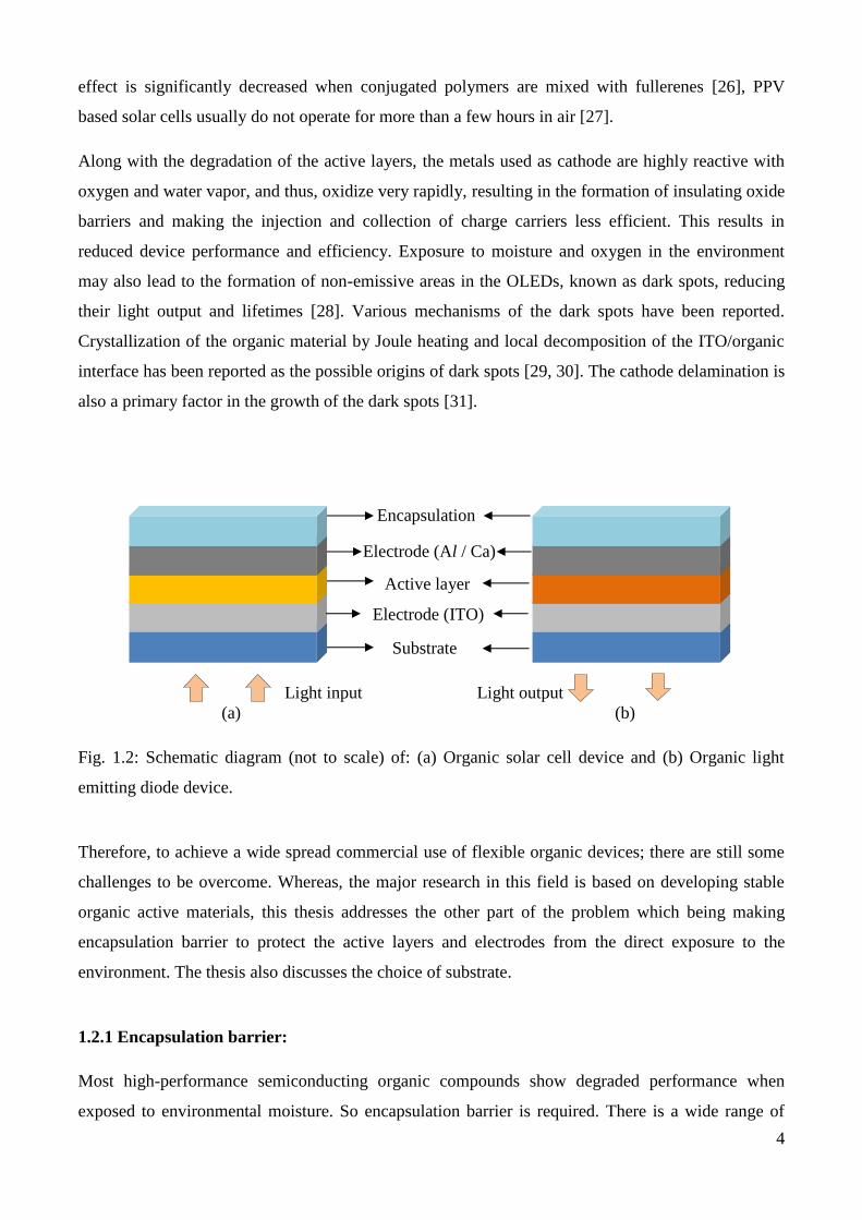
devices usually consist of a substrate and an active layer sandwiched between a transparent anode
(with high work function) and a low work function metal cathode, as shown in Fig. 1.2. The device
structure is completed with some form of encapsulation above the cathode. If the substrate is
permeable, as is the case with most flexible plastic materials, then an additional permeation barrier
below the device layers is also necessary [18].
In these devices, the active layers exposed to the atmosphere, deteriorate rapidly and lead to the
whole device failure. Efficiencies up to 8% have been reported for conjugated polymer [19], while
efficiencies up to 8 to 10% [20, 21] have been reported for small molecule based photovoltaic
devices respectively. Conjugated polymers are known to be unstable in air [22] and susceptible to
photo-degradation induced by oxygen and moisture [23]. By example, Poly (p-phenylene vinylene)
(PPV) and its derivatives are very sensitive to atmosphere. In this case, the oxygen atoms are bonded
to vinyl bonds and break the conjugation and lead to the formation of carbonyl groups [23, 24]. As
shown by spectroscopic ellipsometry results, during the simultaneous exposure to air and light, the
thickness of the active layer increases, while its refractive index and optical absorption coefficient
drastically decrease which leads to the PPV degradation [25]. In spite of the fact that the degradation
4
effect is significantly decreased when conjugated polymers are mixed with fullerenes [26], PPV
based solar cells usually do not operate for more than a few hours in air [27].
Along with the degradation of the active layers, the metals used as cathode are highly reactive with
oxygen and water vapor, and thus, oxidize very rapidly, resulting in the formation of insulating oxide
barriers and making the injection and collection of charge carriers less efficient. This results in
reduced device performance and efficiency. Exposure to moisture and oxygen in the environment
may also lead to the formation of non-emissive areas in the OLEDs, known as dark spots, reducing
their light output and lifetimes [28]. Various mechanisms of the dark spots have been reported.
Crystallization of the organic material by Joule heating and local decomposition of the ITO/organic
interface has been reported as the possible origins of dark spots [29, 30]. The cathode delamination is
also a primary factor in the growth of the dark spots [31].
(a) (b)
Fig. 1.2: Schematic diagram (not to scale) of: (a) Organic solar cell device and (b) Organic light
emitting diode device.
Therefore, to achieve a wide spread commercial use of flexible organic devices; there are still some
challenges to be overcome. Whereas, the major research in this field is based on developing stable
organic active materials, this thesis addresses the other part of the problem which being making
encapsulation barrier to protect the active layers and electrodes from the direct exposure to the
environment. The thesis also discusses the choice of substrate.
1.2.1 Encapsulation barrier:
Most high-performance semiconducting organic compounds show degraded performance when
exposed to environmental moisture. So encapsulation barrier is required. There is a wide range of
Substrate
Electrode (ITO)
Active layer
Electrode (Al / Ca)
Encapsulation
Light input Light output
5
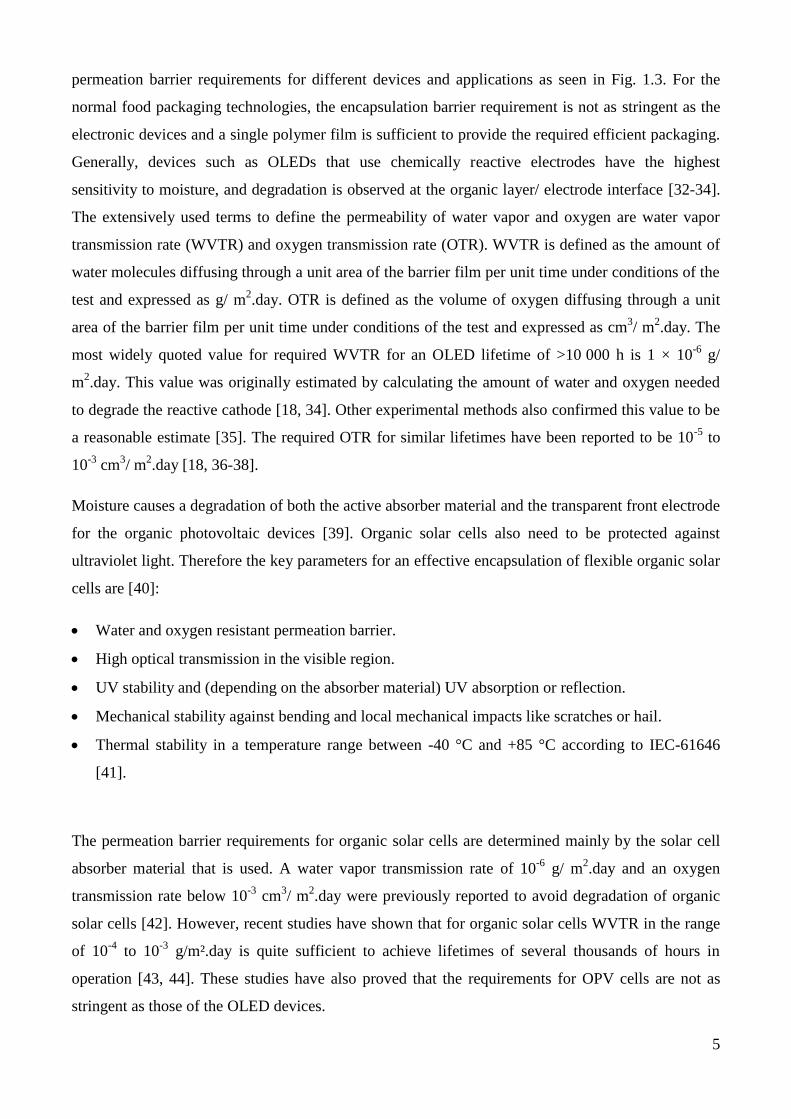
permeation barrier requirements for different devices and applications as seen in Fig. 1.3. For the
normal food packaging technologies, the encapsulation barrier requirement is not as stringent as the
electronic devices and a single polymer film is sufficient to provide the required efficient packaging.
Generally, devices such as OLEDs that use chemically reactive electrodes have the highest
sensitivity to moisture, and degradation is observed at the organic layer/ electrode interface [32-34].
The extensively used terms to define the permeability of water vapor and oxygen are water vapor
transmission rate (WVTR) and oxygen transmission rate (OTR). WVTR is defined as the amount of
water molecules diffusing through a unit area of the barrier film per unit time under conditions of the
test and expressed as g/ m2.day. OTR is defined as the volume of oxygen diffusing through a unit
area of the barrier film per unit time under conditions of the test and expressed as cm3/ m
2.day. The
most widely quoted value for required WVTR for an OLED lifetime of >10 000 h is 1 × 10⁻⁶
g/
m2.day. This value was originally estimated by calculating the amount of water and oxygen needed
to degrade the reactive cathode [18, 34]. Other experimental methods also confirmed this value to be
a reasonable estimate [35]. The required OTR for similar lifetimes have been reported to be 10-5
to
10-3
cm3/ m
2.day [18, 36-38].
Moisture causes a degradation of both the active absorber material and the transparent front electrode
for the organic photovoltaic devices [39]. Organic solar cells also need to be protected against
ultraviolet light. Therefore the key parameters for an effective encapsulation of flexible organic solar
cells are [40]:
Water and oxygen resistant permeation barrier.
High optical transmission in the visible region.
UV stability and (depending on the absorber material) UV absorption or reflection.
Mechanical stability against bending and local mechanical impacts like scratches or hail.
Thermal stability in a temperature range between -40 °C and +85 °C according to IEC-61646
[41].
The permeation barrier requirements for organic solar cells are determined mainly by the solar cell
absorber material that is used. A water vapor transmission rate of 10-6
g/ m2.day and an oxygen
transmission rate below 10-3
cm3/ m
2.day were previously reported to avoid degradation of organic
solar cells [42]. However, recent studies have shown that for organic solar cells WVTR in the range
of 10-4
to 10-3
g/m².day is quite sufficient to achieve lifetimes of several thousands of hours in
operation [43, 44]. These studies have also proved that the requirements for OPV cells are not as
stringent as those of the OLED devices.
6
Fig. 1.3: WVTR requirements for common flexible applications including sensitive electronic
devices [18, 32, 34, 43, 44].
1.2.2 Flexible substrate:
There are several considerations regarding substrate selection for organic devices including Young
modulus, UV stability, dimensional stability, compatibility with process chemicals, moisture uptake
and cost. The leading candidates as substrate materials for organic electronic devices are polymers,
metal foils and ultrathin glass. Thin glass and metal foils both provide the same effective barrier
layers, although a flexible top barrier is still required [18]. The polymeric substrates are considered
better substrates due to their flexibility, lightweight and transparency. But the major disadvantage of
polymeric substrates is that they are permeable to water vapor and oxygen and thus require an
additional barrier layer. The other vital aspect is the processing temperature required by the
subsequent barrier layers, which is generally high, and which the polymeric substrates must be
compatible with. In the endeavor to solve the latter problem the growth temperature for different
inorganic thin film has been reduced [45] and the thermal stability of the polymer substrates has been
improved [46].
OLEDs
Organic
Solar cells
Flexible LCDs
Inorganic Solar cells
Packaging films for food and technical products
102
10-1
10-2
10-3
10-6
WVTR
(g/m2.day)
Encapsulation
Pyramid
10-4

7
1.3 MEASUREMENT OF PERMEATION RATES:
Permeation of oxygen and water vapor is usually measured with standard equipment from Mocon
[47] and Brugger [48]. The two types of equipment have a measurement range starting at 0.0005 g/
m2.day and 0.005 g/ m
2.day respectively [49]. The permeated species are detected by a coulometric
sensor and electrolysis, respectively for the two instruments form Mocon and Brugger. However,
none of the commercially available systems based on these techniques meet the sensitivity
requirements for the low permeation rates required by OLEDs [18]. Therefore new techniques have
been developed. One approach is the Calcium corrosion test, where an opaque metal such as Calcium
is oxidized by the reaction with oxygen and moisture and becomes transparent and insulating.
Measuring the optical transparency, the electrical conductivity or using mass spectrometry, the
permeation rate is assessed [43, 44, 49-62]. Reported effective transmission rate sensitivity for water
vapor through barrier films using the Ca-test are as low as 10-6
g/ m2.day [54, 58, 60-62] and 10
-7 g/
m2.day [56, 59]. Although, the calcium test has the advantage of discriminating between bulk
permeation and defect based permeation, it does not discriminate between oxygen and water vapor
permeation. Permeation techniques using an ultra-high vacuum have been used to obtain OTR
(oxygen transmission rate) measurements as low as 1 × 10⁻⁶
cm3/ m
2.day by a residual gas analyzer.
But the same technique for water vapor is very difficult due to the longer pumping times [18, 49].
To measure reliable water transmission rate, the other approach that is used is known as the tritium
transmission rate (TTR) measurement using a radioactive HTO (hydrogen-tritium-oxygen) tracer
method [49, 63-65]. HTO is the source of tritium that can diffuse through the films either as
molecular HTO or possibly as tritium atoms. The detection limit of WVTR is below ~1 × 10⁻⁶
g/
m2.day.
1.4 ENCAPSULATION BARRIER TECHNOLOGY:
Before the development of organic electronic technology, most of the encapsulation barrier research
was for sensitive food and medicinal packaging. As discussed above, the requirement for
encapsulation barrier for those applications is not quite rigorous and requires a WVTR in the range
between 1 - 40 g/ m2.day. Thin monolithic polymeric films are quite sufficient for such applications.
The basic research in the field of barrier technologies for food and medicines provide the basic
concepts for developing ultra-high efficiency barrier technology required for the sensitive organic
electronic devices. A number of methods currently exist for the encapsulation of organic electronics,
including the hermetic sealing of devices fabricated on glass substrates using a metal or glass lid.
While these structures can protect organic devices from water vapor and oxygen effectively, such

8
packaging architectures are not amenable to flexible applications where the devices are based on
flexible polymer substrates, which is a major thrust area for future organic electronics. Hence,
instead of rigid encapsulation, thin film encapsulation is attractive because of its flexibility and light
weight. However, there exist several constraints on the development and utilization of thin film
encapsulation. The desirable characteristics for the permeation barrier films are their high density,
limited defects, good adhesion, thermal stability and uniform thickness. Moreover high electrical
resistivity, high transparency and low residual stress properties are needed for these materials.
Additionally, they must be deposited at low temperatures in order to be compatible with the plastic
substrates [40]. Throughout the past few decades, the development of highly efficient barrier layers
for organic electronic devices has been one of the major research areas and most of the research was
based on developing either single-layer thin films or multi-layer or alternating layer thin films to
provide the aspired barrier performance.
1.4.1 Single-layer thin film barrier:
Single-layer thin film encapsulation technology is probably the most popular barrier process because
it reduces the production complexity and the manufacturing costs. Several technologies currently
exists for the development of encapsulating single-layer thin films, such as physical vapor deposition
(PVD), plasma enhanced chemical vapor deposition (PE-CVD), atomic layer deposition (ALD) and
hot wire chemical vapor deposition (HW-CVD). In spite of their lucrative production advantages,
very thin single layers of transparent materials such as silica, silicon nitride or alumina, often used as
barrier layers, contain extensive pinholes through which water molecules can diffuse up to the
organic device surface and thus deteriorate the device performance [35, 66-68]. The development of
defects, pin holes or micro-voids occurs due to the poor cleaning process of the substrate, the
processing conditions and the lowering of the substrate temperature to be compatible with the
underlying polymeric substrate. The surface mobility of precursors during deposition goes down with
substrate temperature; higher porosity and a higher density of pinholes are expected in low
temperature thin films compared to the high temperature ones [69]. An arbitrary classification based
on three different types of defects in single-layer thin films as shown in Fig. 1.4, their respective
contributions depend on the size of the permeant molecules (usually 0.2 - 0.3 nm in size), and the
number and size of each class of defect; (a) unhindered transport through ‘macro-defects’ (> 100
nm), (b) hindered transport through ‘nano-defects’ (1 - 10 nm), and (c) hindered transport through
the amorphous lattice of the film (interstice < 1 nm) [70]. Copious amount of research has been
focused on minimizing the number and size of defects in a single layer coating.

9
Fig. 1. 4: A schematic diagram showing the different gas transport pathways through different types
of defects inside single-layer thin film [70].
The leading barrier technology in the industries is based on development of thin films using the PE-
CVD method. Most of the barrier films are based on bulk oxides, nitrides or oxynitrides. Although
all these materials offer barrier encapsulation properties compared to the bare substrates, their
performance is mainly limited by the large defect densities. Commonly used silicon oxide or silicon
nitride deposited by PE-CVD systems, show a WVTR of 0.01 g/ m2.day, which is several orders of
magnitude greater than the targeted requirements [71-74].
Compared to the existing technologies, ALD has shown remarkable achievement towards making
thin film barrier technology. Several researchers have shown promising single-layer encapsulation by
ALD grown Aluminum Oxide (Al2O3), due to their conformal deposition, low defect density and
ability to be deposited at low substrate temperature [75-77]. The effective WVTR value measured for
ALD grown 25 nm of Al2O3 is 1.7 × 10⁻⁵
g/m2.day [52], which is sufficient for the longer lifetimes
for both OPV and OLED devices. Recently, Yang et al. has reported that Al2O3 grown by ALD has a
WVTR value of 8.7 × 10⁻⁶
g/m2.day [78]. This value is the best barrier value for a single layer film
within the best of our knowledge. Other than using Al2O3, Seo et al. reported a WVTR of 6 × 10⁻⁴
g/m2.day using ALD grown TiO2 films [79]. Although ALD grown films shows promise of good
barrier performance, the processing method is quite slow (~1 nm/min) compared to the other CVD
methods (PE-CVD, HW-CVD) and the number of materials that can be deposited using ALD is
limited.
lattice-defect
< 1 nm
nano-defect
1 – 10 nm
macro-defect
>100 nm
Polymer substrate

10
Some researchers used HW-CVD method to deposit single layer films on plastic substrates. This
technique offers many advantages compared to conventional PE-CVD method, like low substrate
damage (due to absence of ion bombardments) during processing, low hydrogen content (or high
density) of the deposited material and conformal step coverage [60-62, 69, 80-86]. HW-CVD also
allows faster growth rate compared to ALD method. Heya et al. has reported HW-CVD grown SiNx
single-layer coating of a polyethylene terephthalate (PET) substrate at 100 °C and they obtained a
WVTR of 0.01 g/m2.day [85]. Kim et al. demonstrated high density SiNx passivation layer deposited
by catalyzer-enhanced CVD method at a substrate temperature of 50 °C and achieved a WVTR of (2-
6) × 10-3
g/m2.day [87]. The SiNx films with thickness of 50 nm were prepared by HW-CVD method
on the cyclic olefin copolymer (COC) and the PET substrates. MOCON and Ca degradation test
measurement resulted in a WVTR value of 0.02 g/m2.day for PET and 0.006 g/m
2.day for COC after
SiNx deposition [88]. Hiroshi Nakayama et al. have developed a single layer of amorphous SiCN
grown by organic Cat-CVD (Catalytic CVD) method with a thickness of 100 nm and they have
measured the permeation value less than 1 mg/m2.day. This value changed from 5 × 10
-1 g/m
2.day to
1 × 10⁻³
g/m2.day, corresponding to the W-filament temperature increase from 100 °C to 1200 °C
[89].
1.4.2 Multilayer thin film encapsulation
As the limited performance of single-layer thin film encapsulation is mainly due to their high defect
densities, the number of defects must be reduced or the effect of defects must be minimized [40].
Multilayer or alternating layers of thin films are widely used to minimize the propagation of defects
or pinholes from one single-layer to the next single-layer film and thus improving the overall barrier
performance of the structure [18, 35, 90-92]. The propagation of defects are interrupted using either a
multi-layer structure of the same inorganic thin-film or alternating-layer structure of two different
inorganic thin films or hybrid layer structure of inorganic / organic thin films. The idea is to hinder
the propagation of pinholes and create a tortuous diffusion pathway for the diffusing permeant
molecules through the barrier, as shown in Fig. 1.5.

11
Fig. 1.5: Schematic diagram of multilayer or alternating layer barrier structure. The intermediate
layer is either inorganic thin film (several nm) or organic thin layer (several nm to µm).
The most effective commercialization of encapsulating barrier technology is based on making hybrid
layer structure consisting of two hard inorganic thin films separated by a soft organic layer. The
organic layer hinders the propagation of defects and makes the diffusion path more circuitous, while
absorbing the stress induced inside the inorganic layers and thus making the whole structure more
flexible. The BarixTM
encapsulation coating from Vitex Inc. has reported an estimated effective
WVTR equivalent to 2 × 10⁻⁶
g/m2.day at ambient conditions measured using Ca corrosion tests [38].
This geometry uses several dyads (pair of organic and inorganic layer) of PVD grown AlOx and UV
curable acrylate monomers which can be deposited in a roll-to-roll process in vacuum. General
Electric has developed a graded barrier layer by PE-CVD [93, 94], consisting of an organosilicon
(SiOxCy) and inorganic SiOxNy alternating layers deposited by PE-CVD. The reported effective
WVTRs for various graded films range from 5 × 10⁻⁶
g/m2.day to 5 × 10
-5 g/m
2.day. Recently, Tera
Barrier Films has developed an alternating layer structure consisting of inorganic oxide layers and
intermediate nanoparticle sealing layer to fill-up the pinholes inside the inorganic layers by the
nanoparticles. The reported barrier performance for this structure is 10-6
g/m2.day [95]. Akedo et al.
have demonstrated an OLED device lifetime of >1000 h at 85 °C using monolithic thin film
encapsulation consisting of PE-CVD SiNx / plasma-polymerized CNx:H multilayer stack [96]. T.-N.
Chen et al. reported that the effective WVTR of their combined SiOx / SiNx / parylene barrier
structure on polycarbonate substrates was found to be 2.5 × 10⁻⁷
g/m2.day at 25 °C and 45 % RH
[91]. These values are to the best of our knowledge the lowest effective WVTR measurements
reported. Chwang et al. reported the lifetime for encapsulated phosphorescent OLEDs (PHOLEDs)
fabricated on glass and barrier coated plastic substrate as 3700 h and 2500 h respectively at ambient
condition [92]. This encapsulation consists of 4-5 pairs of alternating Al2O3 and polyacrylate.
Lungenshmied et al. used alternating SiOx and organosilicon deposited by PE-CVD on the PEN
substrate [97]. Yoshida et al. used a UV curable resin / SiON layer pairs as a moisture barrier film to
achieve the desired OLED barrier performance [98]. Seo et al. has demonstrated ALD grown
nanolaminate layer structure comprising of Al2O3 / ZrO2 with WVTR of 2 × 10⁻⁴
g/m2.day [99]. The
Permeant molecules
Polymer substrate
Inorganic layer Organic layer Inorganic layer
12
same group has shown extremely bendable hybrid encapsulation layer consisting of ALD grown
Al2O3 and plasma polymerized layers with effective WVTR of 10-4
g/m2.day even after 10 000 times
of bending [100]. Multilayer dyads composed of silica nano-particle embedded hybrid nano-
composite (S-H) and ALD grown MgO has demonstrated excellent barrier properties with WVTR of
4.33 × 10⁻⁶
g/m2.day [101]. Ogawa et al. has prepared Cat-CVD grown SiNx / SiOxNy stacked films
to protect OLEDs and they succeeded in maintaining the initial intensity over 1000 h under 60 °C
and 90% RH, which is equivalent to 50 000 h in normal temperature and humidity conditions [84].
The improvement of the barrier properties is due to the blocking of propagation of pinholes from the
underlying SiNx layer by the less dense and flexible SiOxNy layer. Recently, Spee et al. has reported
a hybrid layer structure consisting of SiNx and PGMA layers, where the inorganic thin film was
deposited inside a HW-CVD reactor and the organic layer was deposited inside an initiated CVD
(iCVD) reactor. Their reported WVTR was 5 × 10⁻⁶
g/m2.day which was sufficient for the longer
lifetimes for OLED devices [69].
1.5 OBJECTIVE AND ORGANIZATION OF DISSERTATION:
The reliability issues of the organic electronic devices must the solved in order for their wide spread
commercialization. As discussed above, the thin film technology is the most promising encapsulation
method due to its light weight, flexibility and low cost roll to roll production. Hence, the primary
objective of this present work is developing ultra-high barrier encapsulation structure using the thin
film technology to be incorporated in real organic electronic devices.
In this work silicon nitride (SiNx:H) thin films have been chosen as an effective inorganic barrier
material. The benefit of SiNx:H films over other oxide materials is that it does not require reactive
oxygen atoms in the deposition process, which could react in an undesirable manner with the
underlying polymer substrates. The advantage of SiNx:H over other metal nitrides is that it is more
transparent and also that gaseous precursors for plasma-based deposition are more readily available,
e.g., in the form of silanes [102]. The present research work is divided into two separate parts
consisting of two different barrier technology methods.
The major part of the present work is based on a unique process of formation of barrier method
consisting of deposition of multilayer stack of SiNx:H single-layers deposited on Polyethylene
terephthalate (PET) substrates, each single-layer being surface-treated by low energy Argon plasma
treatment. We have chosen Hot Wire Chemical Vapor Deposition (HW-CVD) method to deposit the
SiNx:H films because of the lower hydrogen content inside the film and its higher density compared

13
to the conventional material obtained by plasma assisted CVD techniques and it’s faster growth rate
compared to ALD method. The idea behind the use of the Argon plasma surface treatment between
two successive SiNx:H single-layers is to hinder the propagation of the pinholes from one single-
layer to the other. The ionic bombardment by low energy Argon ions on the surface of the SiNx:H
thin films makes an atomic relocation at the interface and a smoothing of the surface, which impedes
the diffusion of permeant molecules throughout the whole layer thickness.
The second part of the thesis deals with the development of the conventional alternating layer
structure containing inorganic / organic / inorganic thin layers. The first portion of this work consists
of the alternating layer stacks composed of Matrix Distributed Electron Cyclotron Resonance
(MDECR)-PECVD grown SiNx:H films separated by a spin-coated PMMA [Poly (methyl
methacrylate)] polymer layer. The use of MDECR-PECVD technology for deposition of optical thin
films offers several advantages over conventional radio frequency capacitive-coupled PECVD, such
as faster growth rates, superior control of the deposition process, relatively low ion bombardment
energy and the possibility to use lower substrate temperatures [103-105]. The PMMA polymer is
chosen because it is widely used and inexpensive. Next the alternating layer stacks composed of
HW-CVD grown SiNx:H films separated by a spin-coated PMMA polymer layer is presented in
order to compare the barrier properties with the MDECR PE-CVD grown samples.
The barrier layers have been characterized using different characterization methods which includes
the structural, morphological, optical and mechanical characterizations. Utilizing the electrical Ca
corrosion method to quantify ultra-low permeation through these films is discussed. Finally,
permeation mechanism through these films is demonstrated and discussed.
After the general introduction (chapter 1), chapter 2 consists of brief descriptions of the film
deposition techniques as well as all the characterization methods used in this thesis. The growth
mechanisms and characteristics of the HW-CVD grown SiNx:H films are discussed in Chapter 3.
Chapter 4 describes the main part of this thesis, i.e. the barrier properties of the Argon plasma treated
SiNx:H films and their simple physical interpretation deduced from the experimental study of
permeation barrier versus several parameters. The conventional inorganic / organic hybrid layer
barrier structures and their properties are introduced in Chapter 5. Chapter 6 consists of combination
of two separate encapsulation methods and application of barriers on OLED devices. Finally all the
studies discussed throughout this thesis are summarized in Chapter 7.

14
CHAPTER 2
EXPERIMENTAL TECHNIQUES
This chapter is devoted to the experimental techniques used in this study. Firstly, the film deposition
techniques and plasma treatment technique are described. Next, the characterization techniques
(morphological, structural, optical, electrical and mechanical) are described. Finally, the specific
technical points are summarized.
2.1 BARRIER FILM DEPOSITION SYSTEMS
The amorphous silicon nitride (SiNx:H) thin films studied throughout this thesis as a permeation
barrier layer, have been deposited using Hot Wire Chemical Vapor Deposition (HW-CVD) system
for the most part. The argon plasma treatment between each successive SiNx:H single-layer films to
reduce the water molecule permeability, which is the main objective of this thesis, is carried out
inside a glow discharge radio frequency plasma enhanced chemical vapor deposition system. In the
organic- inorganic hybrid structure which is another part of this thesis, the organic polymer film is
grown by widely used spin coating technique. A minor part of this thesis is devoted to the
development of inorganic-organic hybrid structure, where the inorganic (SiNx:H) layer is deposited
by Matrix Distributed Electron Cyclotron Resonance Plasma Enhanced Chemical Vapor Deposition
(MDECR-PECVD) system in order to compare the barrier properties with HW-CVD grown samples.
The sequence of HW-CVD film deposition and the argon plasma treatment is carried out in a twin
chamber CVD system situated inside a clean-room located at International Iberian Nanotechnology
Laboratory, Braga, Portugal, under the supervision of Prof. Alpuim. The twin chamber CVD system
is described first. This is followed by descriptions of MDECR-PECVD system situated at LPICM,
Ecole Polytechnique, France under the supervision of Dr. Bulkin. The organic layers are deposited
by spin-coating system which is described after that.
2.1.1 Twin chamber CVD system
The twin chamber CVD system consisting of both HW-CVD and PE-CVD reactors are shown in Fig.
2.1 (a) and the pictures of the HW-CVD reactor and PE-CVD reactor are shown in Fig. 2.1 (b) and
(c) respectively. This is an ultra-high vacuum CVD system. The system is equipped with cold-
cathode Penning gauges for measuring the base pressure inside each of the three chambers (including
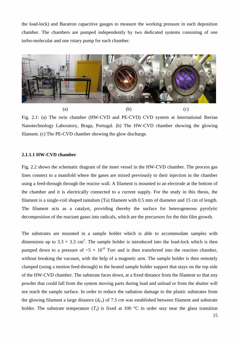
15
the load-lock) and Baratron capacitive gauges to measure the working pressure in each deposition
chamber. The chambers are pumped independently by two dedicated systems consisting of one
turbo-molecular and one rotary pump for each chamber.
(a) (b) (c)
Fig. 2.1: (a) The twin chamber (HW-CVD and PE-CVD) CVD system at International Iberian
Nanotechnology Laboratory, Braga, Portugal. (b) The HW-CVD chamber showing the glowing
filament. (c) The PE-CVD chamber showing the glow discharge.
2.1.1.1 HW-CVD chamber
Fig. 2.2 shows the schematic diagram of the inner vessel in the HW-CVD chamber. The process gas
lines connect to a manifold where the gases are mixed previously to their injection in the chamber
using a feed-through through the reactor wall. A filament is mounted to an electrode at the bottom of
the chamber and it is electrically connected to a current supply. For the study in this thesis, the
filament is a single-coil shaped tantalum (Ta) filament with 0.5 mm of diameter and 15 cm of length.
The filament acts as a catalyst, providing thereby the surface for heterogeneous pyrolytic
decomposition of the reactant gases into radicals, which are the precursors for the thin film growth.
The substrates are mounted in a sample holder which is able to accommodate samples with
dimensions up to 3.3 × 3.3 cm2. The sample holder is introduced into the load-lock which is then
pumped down to a pressure of ~5 × 10⁻⁶
Torr and is then transferred into the reaction chamber,
without breaking the vacuum, with the help of a magnetic arm. The sample holder is then remotely
clamped (using a motion feed-through) to the heated sample holder support that stays on the top side
of the HW-CVD chamber. The substrate faces down, at a fixed distance from the filament so that any
powder that could fall from the system moving parts during load and unload or from the shutter will
not reach the sample surface. In order to reduce the radiation damage to the plastic substrates from
the glowing filament a large distance (df-s) of 7.5 cm was established between filament and substrate
holder. The substrate temperature (Ts) is fixed at 100 °C in order stay near the glass transition

16
temperature of the plastic substrates. The substrate temperature is measured with a thermocouple
embedded in the stainless steel substrate-holder, close to the substrate. During the filament heating
time, a shutter is moved to the closed position in order to protect the substrate from the spurious
species emitted from the filament.
The reactor is equipped with eight lines of different process gases. The source gases are mixed in a
manifold and injected in the chamber through the side wall. The flow rates are controlled by mass
flow controllers.
The three chambers (HW-CVD, PE-CVD and load-lock) are separated by gate valves. This gate
valve system allows transferring the samples from chamber to chamber with the help of a magnetic
transfer arm that stays parked in the load lock during depositions. In this way any sequence of
SiNx:H depositions and argon treatments can be performed without ever breaking the vacuum.
The deposition of thin films was performed in several steps as discussed below:
i) The substrate is fixed inside the substrate holder and then is loaded into the load lock which is
then pumped down to ~5 × 10⁻⁶
Torr before the substrate holder is transferred into the HW-
CVD chamber using the magnetic arm.
ii) The substrate holder is resistively heated to the substrate deposition temperature (Ts) by the
embedded resistor in the sample holder support, connected to a thyristor and controlled by a
Eurotherm controller. The temperature reading for the feedback allowing the system to
operate in closed loop control mode is provided by a thermocouple also embedded in the
substrate holder support.
iii) Filaments are degassed under hydrogen atmosphere for several minutes at a very high
temperature corresponding to a certain filament current value to obtain desired filament
temperature (Tf) (2000 °C). The shutter is kept closed in this step to protect the substrate.
iv) A mixture of source gases is injected when Ts actual reading was identical to the set point and
stable. The shutter remains closed.
v) The shutter is opened to start the deposition at a stabilized substrate temperature (Ts).
vi) At the end of the deposition, the shutter is closed and gas flow is stopped. The filament is
slowly turned off and the heating of the substrate is also turned off.
There are several parameters which are varied in order to obtain optimized growth condition for
SiNx:H deposition. The details of growth mechanism and the growth optimization parameters and
process are discussed in chapter 3.

17
Fig. 2.2: Schematic diagram (not to scale) of the HW-CVD chamber.
2.1.1.2 RF PE-CVD chamber
The sequence of SiNx:H deposition and the argon plasma surface treatment is carried out by moving
the sample between chambers inside the twin chamber CVD system. After the deposition of SiNx:H
thin film inside the HW-CVD chamber, the sample is transferred to the PE-CVD chamber through
the gate-valve without breaking the vacuum.
The reactor is part of a twin chamber system and is described above. Fig. 2.3 shows the schematic
diagram of the inner vessel. It is similar to the HW-CVD reactor except that the filament electrode is
replaced here by the RF electrode (anode) which is a stainless steel disc situated inside and at the
bottom of the chamber. The substrate holder support is used as the top electrode (cathode) and is
grounded to earth. The bottom electrode is connected through an electrical feed-through to the
external RF circuit (see figure) consisting of a 13.56 MHz RF generator, a matching box consisting
of variable capacitances and inductances and an attenuator to allow the 500 W RF power supply to
be operated at about its midrange for better stability and control. The dimensions of the electrodes
are 20 cm2 and the adjustable inter-electrode distance used is 2.5 cm. The self-bias voltage that
develops at the electrode is measured by the control electronics and is part of the matching box self-
tuning control circuit. The same sample holder used for the HW-CVD chamber is used for the PE-
CVD chamber. The sample holder is clamped to the top electrode of the reactor and connected to an
independent electrical heating circuit similar to the one used for the HW-CVD chamber. The
Substrate holder Substrate
Shutter
Reactor wall
Filament
Gas sources
Pump-out 7.5
cm
15 cm
Thermo-couple

18
substrate temperature (Ts) is fixed at 100 °C in order to be compatible with the work on plastic
substrates. The substrate temperature is measured with a thermocouple embedded in a stainless steel
substrate-holder, close to the substrate. Electrical measurements are performed with a 2-channel 60
MHz Digital Oscilloscope Agilent in order to measure the voltage drops at different points in the RF
circuit (see schematic circuit drawing).
There are several parameters which are varied for the surface plasma treatment method. The details
of parameters and their respective effects on the overall permeation barrier properties are discussed
in Chapter 4.
Fig. 2.3: Schematic diagram (not to scale) of the PE-CVD reactor for the argon treatment.
2.1.2 Matrix Distributed Electron Cyclotron Resonance PECVD (MDECR-PECVD)
The MDECR-PECVD Venus system available at LPICM, Ecole Polytechnique is used in a short part
of this thesis for the development of inorganic SiNx:H thin film to fabricate inorganic / organic /
inorganic hybrid structure. The dedicated MDECR-PECVD system is a high density plasma CVD
system and allows faster growth rates, superior control of the deposition process, relatively low ion
Sample holder Sample
Reactor wall
Electrode
Gas sources
Pump-out
Thermo-couple
C-Load
C-Tune L
Matching box
10.67 dB
Attenuator
RF generator
~
2.5
cm
20 cm2

19
bombardment energy and the possibility to use lower substrate temperatures as compared to the
conventional capacitive-coupled PE-CVD system [103].
The reactor is composed of a 50 litre cylindrical vacuum chamber and a turbo-molecular pump as
shown in Fig. 2.4 (a) and (b). The reactor is equipped with two 2.45 GHz magnetron generators to
supply the microwave power. The microwave power is fed into the reactor using flexible coaxial
cables to a set of 16 microwave antennas. The antennas are integrated with a SmCo5 permanent
magnet and arranged in 4 × 4 matrix configuration. The antenna to the substrate holder distance is
approximately 12 cm and the substrate holder (22 cm diameter) is kept horizontally inside the reactor
chamber. A gas distribution ring injects the precursor gases uniformly onto the substrate area [104].
The detailed microwave antenna matrix configurations and the deposition procedure and mechanism
were already discussed extensively in a previous dedicated thesis [105] and previous publications
[103, 104]. In this present thesis, the amorphous SiNx:H thin film as a permeation barrier layer was
deposited utilizing the previous optimized deposition conditions. The SiNx:H films are deposited on
cleaned PET substrates at room temperature and low pressure (2 mTorr) in the MDECR-PECVD
reactor with 1000 W microwave power with a deposition rate of ~6 Å/s. The precursor gases SiH4
and N2 are injected into the reactor through the gas distribution rings with gas flow rates of 10 sccm
and 80 sccm respectively.
(a)

20
(b)
Fig. 2.4: (a) The MDECR-PECVD Venus system at LPICM, Ecole Polytechnique. (b) Schematic
diagram (not to scale) of the deposition reactor.
2.1.3 Spin coating
Spin coating is a widely used technique for the deposition of thin films. A typical process involves
depositing drop of material solution onto the middle of the substrate and spinning the sample with
different spinning parameters followed by a drying process. Due to the centripetal acceleration, the
solution spreads over the entire substrate growing a thin layer of the material. The film thickness on
the substrate depends on the solution density and the speed of the rotation.
The typical spin-coater system consists of a rotating plate (chuck) on top of a rotator. The entire
system is covered by a glass cover to avoid the spreading of the solution outside the system. The
chuck is integrated with a needle-hole creating small vacuum to stabilize the substrate while
spinning. The rotation speed, acceleration and time are controlled by an outside electronic system.
Substrate
ECR region
Pum
p o
ut
Substrate holder Gas sources
Microwave
Connections
Microwave
antenna & magnets
Impedance
Matching unit
22 cm 12 c
m
Injection of
oxidants

21
(a) (b)
Fig. 2.5: (a) The spin-coating system inside the glove-box at LPICM, Ecole Polytechnique. (b)
Schematic diagram (not to scale) of the operation of the system.
In order to develop alternating hard-soft inorganic / organic like structure, polymer layers are
deposited by spin-coating technique inside the glove-box between two inorganic layers. The
commercially available PMMA [Poly (methyl methacrylate)] (from Sigma Aldrich) is dissolved in
chloroform (5 wt. %) and the solution is spin-coated on the already grown SiNx:H film at different
speeds followed by an annealing treatment at 100 °C for 30 min. The optimization of the rotation
speed with the variation of the film thickness and characterization of the film are discussed in chapter
5.
2.2 MORPHOLOGICAL CHARACTERIZATION
2.2.1 Profilometry
Before evaluating the exact optical constants using the spectroscopic ellipsometer, the film thickness
is estimated using a profilometer with the precision of ≈100 Å and with a force of 10 mg. For the
study in this thesis, Dektak 150 profilometer is used to evaluate the film thickness deposited either on
crystalline silicon or glass substrate. At least ten thickness measurements are taken on the film along
the centerline of the substrate to see the homogeneity of the film thickness.
2.2.2 Atomic force microscopy (AFM)
The morphological analysis such as roughness of the barrier films is carried out using the atomic
force microscopy (AFM) technique. A small and sharp nanometer size probe, usually made of silicon
or silicon nitride, mounted on a flexible cantilever moves on the sample surface under van der Waals
Solution
Rotating
Plate
Rotator
Substrate
22
interaction force effect, which is controlled to be constant by keeping the distance between the probe
and the sample surface constant. The scan along the x and y axes and the control of the distance
between the probe and the sample surface along the z axis are generally performed by using
piezoelectric scanners. The cantilever deflection is detected using a laser spot reflected from the
cantilever onto photodiodes.
The measurements are performed using tapping mode of AFM (Integrated Dynamics Engineering) at
a certain frequency for different sizes of the acquisition zones. The tapping mode allows one to carry
out non-destructive measurements without influence of adsorbed layers. The change in frequency
induced by van der Waals interaction force is detected in order to control the distance between the
probe and the film surface.
2.3 STRUCTURAL CHARACTERIZATION
2.3.1 X-ray diffraction (XRD)
X-ray diffraction (XRD) is an instrumental technique that allows determining the crystalline and
amorphous phases of materials. When an incident X-ray beam interacts with the planes of atoms
inside the material, part of the beam is transmitted, part is absorbed by the material, part is refracted
and scattered, and part is diffracted. By applying the Bragg’s law of diffraction, we can measure the
distances between the planes of the atoms that constitute the material. Bragg's Law is n'λ=2d sinθ,
where the integer n' is the order of the diffracted beam, λ is the wavelength of the incident X-ray
beam, d is the distance between adjacent planes of atoms (the d-spacings), and θ is the angle of
incidence of the X-ray beam to the surface. The characteristic set of d-spacings and their intensity
generated in a typical X-ray scan provide a unique "fingerprint" of the phases present in the sample.
When properly interpreted, by comparison with standard reference patterns and measurements, this
"fingerprint" allows for identification of the material. Presence of an amorphous material in the
sample can be determined by occurrence of specific wide halo on diffraction pattern. XRD patterns
shown in this thesis were obtained from measurements performed at room temperature with the Kα
line of Cu radiation with of 1.54 Å issued from an electrical generator (40 kV, 45 mA).
2.3.2 X-ray reflectometry (XRR)
The as deposited and argon plasma treated thin films have been characterized using X-ray
reflectometry method in order to obtain the precise film thickness, the mass density of the films and
surface roughness. This study involves irradiation of a parallel and monochromatic beam of X-ray on
23
the film surface and study the variation of reflected beam intensity with the variation of the angle of
incidence (θ), measured as usual in X-ray scattering, to the surface and not to the normal to the
surface.
In the X-ray field, where the scattering by all the electrons of the solid is important and far from any
absorption, the refractive index (n) of material is less than the refractive index in vacuum and slightly
less than 1. When the X-ray beam is incident on a flat surface with an angle equal to or less than the
critical angle of total reflection (θc), generally 1° maximum, total reflection occurs. This is the reason
why the surface under analysis should be as flat as possible. The refractive index (n) of the material
is given by the following relationship [106]:
𝑛 = 1 − 𝛿 − 𝑖𝛽 (2.1)
𝛿 = (𝑟𝑒λ
2
2𝜋)𝑁0𝜌∑ 𝑥𝑖(𝑍𝑖 + 𝑓𝑖
′)/∑ 𝑥𝑖𝑀𝑖𝑖𝑖 (2.2)
𝛽 = (𝑟𝑒λ
2
2𝜋)𝑁0𝜌∑ 𝑥𝑖(𝑍𝑖 + 𝑓𝑖
′′)/∑ 𝑥𝑖𝑀𝑖𝑖𝑖 (2.3)
re: Classical radius of an electron (2.818 × 10⁻¹⁵
m)
N0: Avogadro number
λ: X-ray wavelength
ρ: Density (g/cm3)
Zi: Atomic number of the i-th atom
Mi: Atomic weight of the i-th atom
xi: Atomic ratio (molar ratio) of the i-th atom
𝑓𝑖′, 𝑓𝑖
′′: Atomic scattering factors of the i-th atom
The value of the parameter δ is very small and ranging from 10-5
to 10-6
for X-rays with wavelength
approximately 1 Å. The critical angle (θc) for total reflection is given by the following formula:
𝜃𝑐 = √2𝛿 (2.4)
The density of the surface film can be deduced by measuring the critical angle for total reflection. At
a given wavelength, for θ > θc, the reflected intensity depends on the density profile
of the interface and decreases rapidly while oscillating. These oscillations, called Kiessig fringes,
result from the interference phenomenon between the waves reflected by the various optical surfaces
(air-film and film-substrate). Their angular positions are dependent on the thickness of the film. The
contrast of the fringes depends on the relative intensity of the two waves, that is to say the respective
indices of the two materials. The period of oscillation depends on the optical path difference between

24
the two waves, allowing deducing the thickness of the film.
X-ray reflectometry (XRR) analyses are carried out on SiNx:H thin-film deposited on crystalline
silicon wafer using a home-made diffractometer under the supervision of Dr. R. Cortes (LPMC,
Ecole Polytechnique). XRR intensities are recorded over each reciprocal space (q) where q=
4πsinθ/λ, and the angular range starting below the critical angle up to 2° with a step size of 0.01° and
using CuKα radiation. The data obtained from the XRR measurements are analyzed using the
Parratt32 software package based on Parratt formalism [107].
2.3.3 X-ray photoelectron spectroscopy (XPS)
X-ray photoelectron spectroscopy (XPS) is an important and extensively used characterization
technique to analyze the surface of films. The method is based on the irradiation of X-ray on the
solids and ejection of electrons due to the photoelectric effect. The electrons carries the information
regarding chemical oxidation states, electronic structure and atomic composition of the solid being
analyzed. The energy distribution of electrons depends on the energy of the X-ray, the binding energy
and work function of the material. Each chemical element being characterized by a single spectrum,
this method allows analyzing precisely the chemical nature of a given material.
For the XPS measurements in this study, Kratos Axis Ultra DLD spectrometer set up situated at
IRAMIS, CEA Saclay, France, is used. A monochromatic Al Kα X-ray source is used with energy of
1486.7 eV with a charge compensation system. Photoelectron data are collected at take-off angle of
90°. Survey spectra are taken at analyzer pass energy of 160 eV and high resolution spectra at pass
energy of 40 eV or 20 eV. The analysis chamber has a base pressure of 10-10
mbar. The spectrums are
calibrated using a known binding energy, in our case carbon, C1s at 285 eV. The spectrometer is
coupled with Eclipse (VG scientific) data acquisition software to analyze the data.
2.3.4 Glow Discharge Optical Emission Spectroscopy (GD-OES)
Glow discharge optical emission spectroscopy is a useful technique recently advancing to analyze the
thin films in more easier and faster way. While it can detect almost all the elements; the detection
limit being down to ppm range. The atomic concentration of elements can be evaluated throughout
the depth profile from 10 nm to 100 µm thickness.
The basic principle of glow discharge is based creating plasma inside very low pressure gas
(typically argon) by high electric field applied across two electrodes. As shown in Fig. 2.6, there are

25
several zones throughout the discharge region and the negative glow (high charge density space) as
well as the cathode dark region (low charge density space) is of particular interest. Electrons
travelling from one electrode to the other collide with the gas atoms forming positive ions. These
ions attracted by the negative potential gain sufficient energy to impinge on the sample surface kept
at the cathode to knock atoms off the film surface. The sputtered atoms are excited by collisions with
more energetic electrons inside the plasma. When these excited atoms are de-excited, they emit
photons with characteristic wavelength. Recording the signal of these wavelengths, the atomic
concentrations of each type of atoms are evaluated [108, 109].
The relative signal intensity of different elements inside the SiNx:H thin films deposited on crystalline
silicon wafers throughout their depth are evaluated using GD-Profiler 2 at Horiba Scientific
(Longjumeau, France). The standard argon plasma is used to study the depth profile. In our
experiments, the operating conditions are: argon pressure of 650 Pa and 30 W RF power. When Ar
atoms are looked for in the films, Neon gas has been used as a plasma source.
Fig. 2.6: Schematic diagram and basic principle of the glow discharge chamber.
2.3.5 Fourier Transform Infrared Spectroscopy
Fourier Transform Infrared Spectroscopy (FTIR) is a non-destructive, widely used technique to
assess the information regarding the chemical composition and atomic bonding in thin films. When a
thin film is exposed to the IR radiation, the sample molecules selectively absorb radiation of specific
wavelength. This absorption gives rise to the change in dipole moment or in other words charge
imbalance of the sample molecules. As a result, the vibrational energy levels of sample molecules
transfer from ground state to the excited energy state, leading to specific absorption peaks in the IR-
spectrum. The FTIR measurements used in this thesis are carried out using a Bruker Equinox 55
spectrometer with wave number range: 370-25000 cm-1
and resolution better than 0.5 cm-1
. The
instrument has a variable temperature cell: 80K – 400K. The instrument is purged with dry nitrogen
Anode Cathode Positive glow Negative glow
Cat
hode
dar
k z
one

26
before the measurement in order to get rid of the absorption peaks corresponding to water or CO2.
The absorption signal due to the substrate is subtracted from the measured data during the analysis.
2.4 OPTICAL CHARACTERIZATION
2.4.1 UV-visible spectroscopic ellipsometry (UV-visible SE)
UV-visible spectroscopic ellipsometry, which is a non-destructive and non-contact optical technique,
is a useful method for assessing the thickness and optical constants of barrier films during and after
deposition [110, 111]. UV-visible spectroscopic ellipsometry measures the change in polarization
state of a light beam after its reflection from the film surface. If a linearly polarized light beam is
incident with an angle φ as defined to the normal to the surface, on a film (refractive index n), the
reflected beam will be elliptically polarized. At each wavelength of the incident beam, the change in
polarization is represented by two parameters: amplitude ratio (ψ) and phase difference (Δ). These
two parameters are related to the complex Fresnel reflection coefficients rs and rp through the
following relation:
𝜌 =𝑟𝑝
𝑟𝑠=
𝐸𝑝𝑟 𝐸𝑝
𝑖⁄
𝐸𝑠𝑟 𝐸𝑠
𝑖⁄= 𝑡𝑎𝑛𝜓𝑒𝑖∆ (2.5)
where Ep and Es the parallel and perpendicular components of the E vector parallel to the plane of
incidence and perpendicular to the plane of incidence, defining the planes of polarization for the
waves. The superscripts i and r corresponds to the incident and reflected beams.
Spectroscopic ellipsometry measurements are carried out by using a phase modulated [112] UV-
visible spectroscopic ellipsometer, UVISEL (Jovin-Yvon), in the photon energy ranging from 1.5 to
5.0 eV. The UV-visible beam is emitted from Xenon lamp and passes through a linear polarizer then
a photo-elastic modulator (50 kHz). After reflection on the sample surface, it traverses through a
second polarizer (placed as an analyzer) and is focused at the entrance slit of a monochromator and
photomultiplier.
In the case of a phase-modulated ellipsometer, the measured parameters are Is and Ic, which are
related to ψ and Δ according to: Is = sin 2ψ sin Δ and Ic = sin 2ψ cos Δ. In order to analyze ψ and Δ,
or Is and Ic data, a model, based on the Abelès matrix approach [113], specific dispersion relation and
the Bruggeman Effective Medium Approximation [114] is used. For developing the structure of the
model, the DeltaPsi II software package supplied by the ellipsometer manufacturer is used.
27
Due to large anisotropy of polyethylene terephthalate (PET) substrate, the optical modeling of the
barrier films deposited on PET substrates is quite impossible. To evaluate the optical constants of
thin films deposited on PET substrates, single-wavelength polarimetric study under Fourier plane is
used to deduce the refractive index [115]. However, the measurement procedure and optical
modeling for the PET substrate are also impossible due to local anisotropy and the study is out of the
scope of the aim of the present thesis. For that reason, all the optical constants used throughout this
thesis are deduced from spectroscopic ellipsometer study on thin films deposited on crystalline
silicon wafer substrates with a substrate thickness of 510 µm. The optical constants of crystalline
silicon are quite well defined.
2.4.2 Integrating sphere
The integrating spheres are used for applications such as highly reflective and anti-reflective
coatings, color correction coatings, band-pass characteristics of UV, visible and near infra-red (NIR)
filters. It is based on homogeneous distribution of multiple radiations by means of multiple
Lambertian reflections. The reflection and transmission measurements of the permeation barrier thin
films are performed using Perkin Elmer Integrating Sphere (LAMBDA 950). This instrument is
useful for performance of wavelengths up to 3300 nm and based on InGaAs photo-detector with
UV/vis resolution of ≤ 0.05 nm and NIR resolution of ≤ 0.20 nm. The reflectance (R) and
transmittance (T) of the permeation barrier deposited on PET substrates are measured using this set-
up to check the compatibility of the barrier films for their utilization as a window layer for organic
optoelectronic devices.
2.5 PERMEATION BARRIER CHARACTERIZATION
The purpose of permeation barrier films is to limit the exposure of organic electronics to water vapor
and oxygen. Thus controlled permeation rate through the barrier films is necessary. Measuring and
quantifying ultra-low permeation rates of water vapor (~10-6
g/m2.day) and oxygen with high
reliability and accuracy is one of the main challenges of characterizing encapsulation films [37, 43,
44, 50-60]. The permeation rates of oxygen and water vapor across the barrier layers are
characterized in terms of the oxygen transmission rate (OTR) and the water vapor transmission rate
(WVTR). Typically, commercial systems are useful for analyzing most single-layer and some of
multilayer films but are not sensitive enough to detect the ultra-low permeation rates of advanced
encapsulation materials. Common coulometric permeation measurements tools are limited to a
sensitivity of 5 × 10⁻⁴
g/m2.day [47] for water vapor and the tritium test provides a higher sensitivity,

28
but requires radioactive substances and large experimental efforts [49, 63-65]. Building an organic
device such as an OLED or OPV represents an involved test procedure with many experimental
parameters, which are difficult to control. Thus, a simple and precise evaluation is essential for the
development of ultra-high barrier encapsulations [57].
The Ca corrosion test is a widely known method for measuring ultra-low permeation rate barrier
films [56, 57, 59]. Calcium is a conducting and opaque metal which becomes non-conducting and
transparent after oxidation [51]. It rapidly oxidizes in air due to the highly negative Gibbs free energy
(G°rxn) of formation of Ca oxides making it very sensitive for detecting the presence of oxygen and
water vapor. Since the oxide is a dielectric and transparent, both of them are possible to monitor the
consumption of Ca by either measuring the change in electrical conductance or in optical
transparency [57]. Hence, the measurement of Ca conductance or transparency changes versus time
provides an indirect method to determine the oxidation and corrosion rates of Ca. In recent years
several groups of experts from academic, public-private research and development labs, implemented
Ca test. According to a recent publication by Reese et al. [56, 59], Table 2.1 comprises all the
implementations of Ca based permeation measurement tests.
References Method Range (g/m2.day) Features
Nisato et al.
[37]
Optical Ca Test 5 × 10⁻⁵
to 1 (21 °C/50% RH)
4 × 10⁻⁷
(85 °C/50% RH)
Can see pinholes/defects in barrier.
High sensitivity.
Edge seal limited
Not commercially available
Kumar et al.
[50]
Optical Ca Test 10-2
(50 °C/95% RH) Temperature dependent measurement
Poor sensitivity
Edge seal limited
Not commercially available
Paetzold et al.
[51]
Electrical Ca Test <5 × 10⁻⁵
(38 °C/90% RH) High sensitivity
Quantitative for uniform films or films
with many defects close to one another.
Parallel in situ measurements possible.
Not commercially available
Carcia et al.
[52]
Optical Ca Test < 10-5
(38 °C/85% RH) High sensitivity
Edge seal limited
Thickness and temperature dependence of
permeation measurement
Not commercially available
Choi et al. [54]
Electrical Ca Test <10-6
to 10 (20 °C/60% RH) High sensitivity.
Quantitative for uniform films or films
with many defects close to one another.
Parallel in situ measurements possible.
Edge seal limited
Not commercially available
Leo et al. [57]
Electrical Ca Test 10-5
to 15 (30 °C/24% RH) High sensitivity
Well discrimination between electrical and
optical measurements
Parallel in situ measurements possible
Result is independent of the variations of
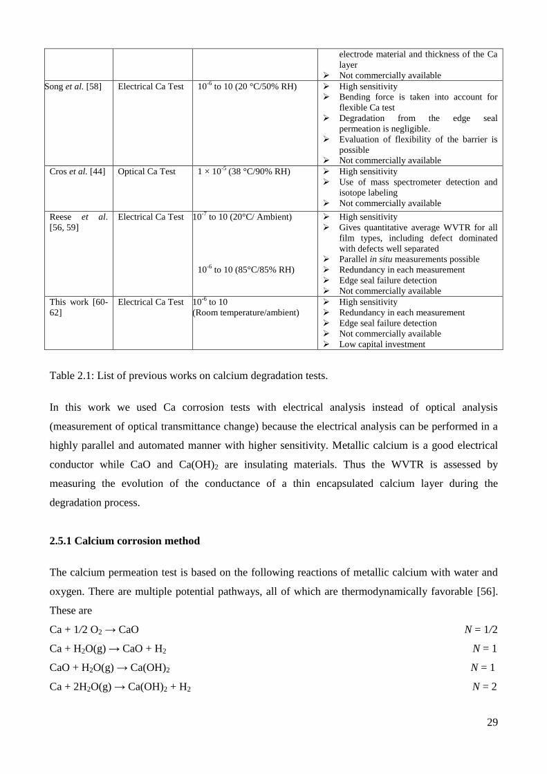
29
electrode material and thickness of the Ca
layer
Not commercially available
Song et al. [58] Electrical Ca Test 10-6
to 10 (20 °C/50% RH) High sensitivity
Bending force is taken into account for
flexible Ca test
Degradation from the edge seal
permeation is negligible.
Evaluation of flexibility of the barrier is
possible
Not commercially available
Cros et al. [44] Optical Ca Test 1 × 10⁻⁵
(38 °C/90% RH) High sensitivity
Use of mass spectrometer detection and
isotope labeling
Not commercially available
Reese et al.
[56, 59]
Electrical Ca Test 10-7
to 10 (20°C/ Ambient)
10-6
to 10 (85°C/85% RH)
High sensitivity
Gives quantitative average WVTR for all
film types, including defect dominated
with defects well separated
Parallel in situ measurements possible
Redundancy in each measurement
Edge seal failure detection
Not commercially available
This work [60-
62]
Electrical Ca Test 10-6
to 10
(Room temperature/ambient)
High sensitivity
Redundancy in each measurement
Edge seal failure detection
Not commercially available
Low capital investment
Table 2.1: List of previous works on calcium degradation tests.
In this work we used Ca corrosion tests with electrical analysis instead of optical analysis
(measurement of optical transmittance change) because the electrical analysis can be performed in a
highly parallel and automated manner with higher sensitivity. Metallic calcium is a good electrical
conductor while CaO and Ca(OH)2 are insulating materials. Thus the WVTR is assessed by
measuring the evolution of the conductance of a thin encapsulated calcium layer during the
degradation process.
2.5.1 Calcium corrosion method
The calcium permeation test is based on the following reactions of metallic calcium with water and
oxygen. There are multiple potential pathways, all of which are thermodynamically favorable [56].
These are
Ca + 1/2 O2 → CaO N = 1/2
Ca + H2O(g) → CaO + H2 N = 1
CaO + H2O(g) → Ca(OH)2 N = 1
Ca + 2H2O(g) → Ca(OH)2 + H2 N = 2

30
where N indicates the reaction ratio. It has been determined using isotopic labeling methods [53] that
at room temperature, the kinetics of corrosion directly from oxygen are significantly slower than that
via moisture. This leaves the complication as to whether or not the reaction ratio of calcium to water
(N) is 1 or 2, or some intermediate level. Previous implementations of the Ca test assumed a reaction
ratio of 2, with limited evidence to support this assumption [37]. According to Reese et al., the
gravimetric studies shows that the final product is completely Ca(OH)2 and thus the value of N is
equal to 2 [56]. In all testing conditions described above in Table 2.1, it is impossible to distinguish
between the contribution from either water vapor or oxygen to the Ca corrosion. As the Ca
degradation from oxygen is significantly slower than that via water vapor, in this thesis, we will
utilize the term WVTR to denote the combined effects of water vapor and oxygen permeation.
2.5.2 Experimental method
To measure the water vapor transmission rate (WVTR) value, we use the electrical calcium
degradation test method [51, 54, 56-60]. All flexible barrier coated substrates are cut to 2.2 × 2.2 cm2
pieces, carefully cleaned and then transferred to a glove box system with active purification. The
cleaning procedure is very important because the particle contaminations on the calcium sensor and
in the encapsulation layers causes defects leading to localized oxidation giving erroneous values of
effective WVTR. The cleaning process employed in this study consisted of three cleaning steps: soft
detergent – deionized (DI) water – nitrogen blowing. The barrier coated substrates are degassed at 90
°C for about 3 hours inside the glove-box prior to the Ca deposition to get rid of integrated water
molecules.
For the Ca degradation test, 100 nm Ca layer with an area of 1.13 cm2 and aluminium contacts (150
nm) are deposited through shadow masks on the back side of the barrier coated substrates using
thermal evaporator (see Fig. 2.7). Deposition rate and thickness are monitored using a calibrated
quartz crystal microbalance near the substrate. A low deposition rate of 0.2 nm/s at a pressure <10-6
mbar is chosen to get a really smooth layer. The Ca layer is then covered with a glass plate and the
edges of which are sealed with epoxy resin (Nagase Chemtex Corp. XNR 5570). The resin is cured
under UV-lamp (365 nm wavelength) inside the glove-box. The water permeation through the epoxy
edge-seal is confirmed to be negligible by using a glass plate as a substrate as discussed later.
Therefore, the Ca layer is on one side of the barrier film and the other side is exposed to the
environment. Water vapor molecules after diffusing through the barrier coated polymer substrate
react with the deposited calcium and thus reduce its conductivity. The change of conductance is
measured using a four point probe technique of Solartron-Schlumberger 7060 Systems Voltmeter

31
(current is injected through the outer probes and the voltage is measured through the inner probes)
and the data is recorded using a LABVIEW system. From the evolution of the conductivity value, the
permeation rate is evaluated.
Fig. 2.7: Schematic diagram (not to scale) of the calcium degradation test set-up (a) side view, (b)
top view.
2.5.3 Calculations
The water vapor permeation through a homogeneous film is usually defined as a combination of
absorption of permeate into the film followed by diffusion of permeate. Therefore, if the diffusion
coefficient (D) is assumed to be constant, the relationship between the diffusion coefficient (D), the
permeation coefficient (P) and the solubility coefficient (S) simplifies to:
Substrate
Barrier Film
Glass cover Epoxy Resin
Al electrodes Ca sensor
Water molecules
Substrate
Glass Cover
Calcium
U I
Al Electrodes
X
Y
I
Z

32
= (2.1)
The solubility and diffusion coefficients are intrinsic material properties and the water vapor
permeation rates of barrier films are usually reported in the unit of g/m2.day at given temperature and
concentration (generally described in relative humidity: RH).
Fig. 2.8: Permeation of water vapor through a film. C, p, l, D and S indicate vapor concentration,
vapor pressure, thickness of the film, and diffusion and solubility coefficients respectively.
The figure 2.8 shows the permeation model and if the film is initially free of the diffusing species,
the initial and boundary conditions for the system can be expressed as [116]:
C (x, 0) = 0; (2.6a)
C (0, t) = C0; (2.6b)
C (l, t) = Cl; (2.6c)
The permeation of water vapor can be described by Fick’s first law of mass diffusion using the
analogy to Fourier’s law of heat conduction. The permeant flux J is proportional to the concentration
as
= −
(2.7)
Where, C is the concentration of the diffusing species and x is the space co-ordinate measured
normal to the section.
D, S
C0 C
l p1
p2
l
Am
bie
nt
air
x=0 x=l

33
Once the mass balance of an element is taken into account, equation (2.7) can be used to derive the
fundamental differential equation of diffusion:
= (
2
2) (2.8)
With the assumption of Henry’s law which relates the concentration, C to the partial pressure, Δp
through the linear relationship = ∆ , the concentration in equation (2.7) can then be replaced
using the solubility coefficient and partial pressure. Under steady state conditions, assuming
diffusion and solubility coefficients to be independent of concentration, the permeation flux can be
expressed as:
= ( 2 )
(2.9)
If the upstream concentration, C0, remains constant during the course of the diffusion process and the
downstream concentration is negligible compared to the upstream pressure (that is Cl ≈ 0), the
solution of equation (2.8) subject to the boundary conditions of (2.6), by either Laplace transform or
separation of variables is given below [117]:
(𝑥 𝑡) = 0 (1 −
) −
2
𝜋∑
(
𝜋
)𝑒 2𝜋2 / 2
(2.10)
Where C0 is a fixed concentration on one side and is the thickness of film. In general, the previous
equations apply to diffusion through a single-layer film.
The mass flux J is obtained by differentiation with respect to distance in accordance with Fick’s first
law. The flux at the downstream surface (x=l) can be integrated over time to give the total mass (Q)
transmitted through the layer per unit area [117]:
(𝑡) = ∫ (𝑥 = 𝑡) 𝑡′ =
−
−
2
𝜋2∑
( )
2𝑒 2𝜋2 / 2
0 (2.11)
The water vapor mass transport rate (Rw) through the barrier film with area Af is given by [56, 59],
= ( )
= (2.12)
The mass consumption rate of calcium, RCa, can be calculated from the mass transport rate of water,
Rw as,
= (
)
(2.13)
where MCa is the atomic mass of calcium, and Mw the molecular weight of water. Negative sign is
used due to the exothermic reaction of Ca with water. For thin Ca layers relative to the diameter of

34
the Ca sensor (nm as compared to cm) one can ignore oxidation of the sides of the Ca sensor such
that,
= 𝛿
(2.14)
Where h is the Ca thickness, ACa is the total Ca sensor area, and the density of Ca (δCa = 1.55 g/cm3).
Combining equations (2.12)–(2.14) yields
= −𝑁𝛿 (
) (
) (
) (2.15)
The resistivity of the Ca sensor is measured using a four point probe technique. So the multiplication
of the effective width (w) by the length (leff) corresponds to the area inside the middle electrodes.
Then the resistance (R) can be approximated by,
= 𝑒
(2.16)
Where ρCa is the thin film calcium volume resistivity and w is the line width. Combining Eq. (2.15)
and (2.16) yields
= −𝑁𝛿 𝜌 ( 𝑒
) (
) (
) [
( ⁄ )
] = −𝑁𝛿 𝜌 (
𝑒
) (
) (
) [
] (2.17)
Where G = 1/R = conductance.
2.5.4 Calibration
The sheet resistance of the Ca sensor is measured with four point probe method. Due to the finite
width (w) and h<<s (where s is the probe spacing), there should be a correction factor. According to
F.M.Smits [118],
= 2 2 (2.18)
Where F1=F1(h/s) is the thickness correction factor (≈1 for h<<s) and F2=F2(d/s) is the finite width
correction factor (≈0.95), d being the diameter of Ca sensor.
There is one more correction factor, Temperature Correction Factor (TCF). The sheet resistance
should be normalized to the value it would be if measured at 23 °C. The TCF is calculated as
follows:
= [1 − ( − 2 )] (2.19)

35
Where T is the measured temperature in °C and TCR is the Temperature Coefficient of Resistance
(for Ca= 0.0041 /°C).
Combining Eq. (2.18)-(2.19),
= 𝑠 𝑒𝑒
2 2 (2.20)
The bulk resistivity ρCa deduced from equation (2.16), is 9 × 10⁻⁸
(Ω.m). This value is reasonable
when compared to literature values for bulk resistivity. Paetzold et al. measured a value of 8.95 ±
0.78 × 10⁻⁸
(Ω.m) [51].
2.5.5 Result computation
Fig 2.9 shows a typical conductance evolution curve. The conductance evolution curve consists of
three different zones:
(a) Lag time zone: Because the water molecules are obstructed by the solid (barrier and the
substrate), the diffusion path is straight along the medium co-ordinate, and hence the true
diffusion path length (lc) is greater than or at least equal to the total length of the barrier coated
substrate (l). The tortuosity factor, τ, is defined as the ratio of true molecular path length to the
displacement of the molecular path along the medium co-ordinate [116].
=
(2.21)
This region which is related to the tortuosity factor, τ, corresponds to the stable region of curve
from the beginning of the measurement to the curvature where the curve tends to go down. The
water molecules after passing through the barrier and then the substrate reach to the calcium
sensor. This region shows the minimum time taken by the water molecules to diffuse through the
whole thickness of the barrier to reach the calcium sensor.
(b) Degradation zone: Water molecules after penetrating through the barrier coated substrate reach
the calcium sensor and react with it to form CaO or Ca(OH)2 as discussed in 2.5.1. Gravimetric
studies have determined that the stoichiometry of the final product is almost completely Ca(OH)2
as discussed above. Because of the tortuosity of the barrier due to the statistical occurrences of
pinholes and defects inside the barrier films (which contribute to the inhomogeneity of the

36
barrier), all the water molecules do not reach the Ca sensor at the same time and they contribute
to the total evolution of the second region until all the Ca is oxidized. So this region corresponds
to the degradation of the sensor from calcium metal into Ca(OH)2.
(c) Saturated zone: This region corresponds to the state when all the metallic calcium is converted
to Ca(OH)2 and no more evolution is observed. In this state the conductance tends to become
negligible.
0 10 20 30 40 500.0
0.2
0.4
0.6
0.8
1.0
32
No
rmal
ized
co
nd
uct
ance
(S
)
Time (h)
Lag-time
WVTR
1
Fig. 2.9: Typical data of evolution of conductance of the calcium sensor with time, showing the three
different zones.
The measurement of lag-time of the barrier is straight forward and is assessed from the first region of
the conductance evolution. Computation of the slope of the second region of Ca degradation to
measure the WVTR value from the raw data obtained from the conductance measurements of Ca
sensor is a little tricky. In literature there are many methods to fit the evolution slope of conductance.
Some of them based on the thermodynamic modeling considering the series resistance (Leo et al.
[57]) and some based on the higher order polynomial fit of the inflection points (Reese et al. [56]).
From most of the literatures it is clear that the slope of evolution to calculate the effective WVTR
should be considered in the degradation region of above figure, as this is the region in which the
metallic calcium after degradation converts to Ca(OH)2. The main difficulty to find the slope is to
determine a single slope for the entire degradation region, which is not the case for most of the
evolutions. In this thesis, an average slope is considered to measure the effective WVTR taking into
account all possible slopes in the degradation region by defining the beginning of decrease of
conductance until the null conductance is reached.

37
2.5.6 Method sensitivity and reproducibility
All the samples are encapsulated with a glass cover on the topside (Fig 2.7). Glass is assumed to be a
perfect barrier and water molecules only penetrate from the barrier side. However, permeation
through the adhesive and along the interfaces between adhesive and glass cover or flexible substrate
limits the sensitivity of the test. To define the background permeation, the electrical calcium test is
performed for a glass substrate. Here the only sources of calcium degradation are diffusion through
the adhesive layer. The test on glass substrate leads to a WVTR of ~10-6
g/m2.day after 10 000 h,
which defines the sensitivity of the test.
The reproducibility is investigated by simultaneously measuring 20 uncoated flexible polyethylene
terephthalate (PET) substrates. For this purpose we use commercial PET films from DuPont Teijin
Films (Melinex ST 504 Film) of 175 µm thickness with one side planarized. It should be noted that
the same commercial PET foils are used as substrates throughout this dissertation. The evolution of
conductance of Ca sensor deposited on bare PET is shown in Fig. 2.10 with a lag time of ~1 h. The
effective WVTR is averaged over 20 such measurements and the result is a WVTR of 0.17 ± 0.05
g/m2.day with a standard deviation of 3.7%. This deviation may be caused by variations in the
substrate cleaning process, the calcium conductivity or thickness and maybe inhomogeneity of the
substrate itself.
0 1 2 3 4 5000 100000.0
0.2
0.4
0.6
0.8
1.0
No
rmal
ized
co
nd
uct
ance
(S
)
Time (h)
glass
bare PET
Fig. 2.10: Evolution of normalized conductance of the Ca sensor for glass substrate and bare PET
substrate.
2.5.7 Technical drawbacks
Although the calcium degradation test set-up proved to be highly sensitive, the measurement is
limited by several technical parameters. Deposition of epoxy resin on top of the calcium surface
should be highly precise. A small air bubble inside the epoxy resin can create inhomogeneous

38
degradation of the calcium, which will lead to either reducing effective lag-time or erroneous
effective WVTR value. To evaluate the homogeneity of the measurements, two different test set-ups
were used, as seen from Fig. 2.11: (a) here the calcium top surface is completely covered by epoxy
resin and (b) calcium top surface is partly covered by epoxy resin with some gas bubbles inside.
However, the second method is not effective due to the impurity inside the glove-box system and the
remaining water vapor and oxygen in the gas bubble react very rapidly with the sensor, leading very
fast degradation and inhomogeneous oxidation; giving almost no effective lag-time and erroneous
WVTR result (Fig. 2.12).
Fig. 2.11: Schematic diagram of calcium tests with: (a) Top side of the calcium is completely
covered by glass plate and (b) Top side of the calcium is partly uncovered by gas volume.
0 100 200 300 400 5000.0
0.2
0.4
0.6
0.8
1.0
Norm
aliz
ed c
onduct
ance
(S
)
Time (min)
Top side completely covered
Top side with gas bubbles
Fig. 2.12: Evolution of normalized conductance of Ca sensors deposited on bare PET substrates.
2.6 MECHANICAL CHARACTERIZATION
The actual purpose of the permeation barrier layers is to protect the sensitive devices based on plastic
substrates for flexible applications. The brittle inorganic materials used as a permeation barrier film
PET Substrate
Gas volume
Calcium
Epoxy resin
Contacts
Glass cover
(a) (b)

39
for multilayer or hybrid layer structures have pinholes or defects which arise due to the processing
conditions. However, the failure mechanics of the layers depends extensively on their mechanical
properties and adhesion towards the underlying layer or the substrate.
The mechanical flexibility of the barrier coated substrates is characterized by bending the structure
for several time cycles with a fixed radius of curvature (r). For the bending test, a home-made
bending machine with a screw system (Fig. 2.13 (a)) is used and the sample is bent for different time
cycles using an automated motor system. The bending of the sample gives rise to tensile strain inside
the films, which in return forms channel cracks by the formation of interfacial delamination of two
consecutive layers (Fig. 2.13 (b)) [119]. Ca degradation test is performed on such samples in order to
verify the bending effect on the permeation barrier properties.
(a)
(b)
Fig. 2.13: (a) Schematic diagram (not to scale) for bending of barrier coated PET substrate inside two
tracks with a fixed radius of curvature. (b) Schematic diagram of the channel cracking and formation
of interfacial delamination.
Barrier coated PET substrate
r
First layer
Substrate
Interfacial
delamination Channel crack

40
2.7 SUMMARY OF CHAPTER 2
The deposition techniques as well as the characterization methods of the thin films to be used as a
permeation barrier are discussed in this chapter. The specific technical points are summarized below:
i) The amorphous SiNx:H thin films to be used as the inorganic layer for the barrier structures are
deposited using HW-CVD and the plasma treatment is carried out in a RF-PECVD reactor.
MDECR-PECVD is also used to deposit amorphous SiNx:H thin films to be used as a barrier
layer. The organic layer of PMMA to be used in fabricating alternating hybrid structure is
deposited by spin-coating technique.
ii) The morphological characterizations of the deposited films are performed with the profilometry
and atomic force microscopy (AFM) techniques. The structural and compositional analysis of the
films are carried out using X-ray diffraction (XRD), X-ray reflectometry (XRR), X-ray
photoelectron spectroscopy (XPS), glow discharge optical emission spectroscopy (GDOES) and
Fourier Transform Infrared Spectroscopy (FTIR) techniques. The optical characterizations are
done with UV-visible spectroscopic ellipsometry and integrating sphere methods.
iii) The permeation barrier properties are evaluated using the electrical calcium test method. The
details of the test method as well as its theoretical background are discussed thoroughly in this
chapter. The sensitivity and reproducibility of this test setup are introduced. Its technical
drawbacks are also summarized.
iv) Finally, the mechanical characterizations of the films are carried out by bending the films for
several cycles.
41
CHAPTER 3
PROPERTIES OF HW-CVD GROWN SILICON NITRIDE
FILMS
3.1 INTRODUCTION
In this work silicon nitride (SiNx:H) thin films have been used as an effective inorganic barrier
material. SiNx:H thin film is one of the most promising and widely used materials for barrier coating
technology [120]. The benefit of SiNx:H films over other oxide materials (SiOx, Al2O3) deposited by
other groups [71, 75-77,79] is that it does not require reactive oxygen atoms in the deposition
process, which could react in an undesirable manner with the underlying flexible substrates. The
advantage of silicon nitride over other metal nitrides is that it is more transparent and also that
gaseous precursors for plasma-based deposition are more readily available, e.g., in the form of
silanes (SiH4) [102]. Although, the low temperature deposition process below 100 °C is required to
be compatible with the flexible plastic substrate (PET), SiNx:H films show low barrier properties as
the deposition temperature decreases. However, the SiNx:H films produced by HW-CVD method at
low temperature are denser than those produced by PE-CVD method and therefore are suitable for
the utilization as barrier films [120]. HW-CVD method is also advantageous compared to ALD
technique, due to its higher deposition rate. SiNx:H films particularly studied by the Japanese
industry [121-124] are prepared with a gas mixture of SiH4, NH3 and H2 using HW-CVD method.
Osono et al. have reported low temperature deposition (below 80 °C) of SiNx:H films using HW-
CVD with very high deposition rate (110 nm/min) [125], thus allowing the possibility to grow high
quality films on compatible plastic substrates. Alpuim et al. have succeeded to produce device
quality SiNx:H films with good dielectric properties at 100 °C with high density and high
transparency [86]. A very high deposition rate (>7 nm/s) was achieved for device quality films by
Verlaan et al [126].
This chapter is devoted to the properties of amorphous SiNx:H films deposited by HW-CVD reactor
on flexible PET substrates. The deposition temperature is fixed at 100 °C to be compatible with the
glass transition temperature of the polymer substrates. First, the optimization of the film growth
procedures is described in detail varying different deposition parameters. This is followed by the
characterizations of the optimized SiNx:H films by different analytical techniques. Finally the water
vapor transmission rates of SiNx:H films which qualify the quality of the permeation barriers for the

42
organic layers composing the different devices of interest (OLEDs and organic solar cells) are
analysed.
3.2 HW-CVD PARAMETERS AND DEPOSITION CONDITIONS
There are several deposition parameters that affect the growth of SiNx:H thin films deposited inside
the HW-CVD chamber [127]. Some of the parameters are interdependent to each other as discussed
below.
3.2.1 Choice of filament material
As a filament wire material, tungsten (W) was widely used throughout the last decades. This is cheap
and the melting point (3422 °C) is very high. However, W wire reacts with the SiH4 at filament
temperature (Tf) up to 1850 °C, developing different phases of W-silicide (WSi2 and W5Si3) [128]
causing W contamination on deposited films, thus reducing the filament lifetime. It has been shown
by Bourée et al. that for a high effective filament surface area (Sf =27 cm2), the W content inside the
microcrystalline silicon films deposited by HW-CVD increases steadily from 5 × 10¹⁴
to 2 × 10¹⁸
atoms/cm3 when the filament temperature Tf increases from 1500 to 1800 °C [129]. To avoid those
contamination issues, it is required to maintain high Tf, and thus the possibility of depositing films at
lower substrate temperature (Ts) using W wire is reduced. Since the year 2005, the W-filament has
been replaced by the tantalum (Ta) wire. The melting point of Ta material is 3017 °C. It is less
reactive with SiH4 at lower temperature and the formation of Ta-silicide (Ta5Si3) takes place at a
lower temperature (up to 1750 °C). Thus it is possible to use a low Tf inducing lower Ts, and there are
lower contamination from the wire material [130] and improved wire lifetime. In this study, the
filament used at INL, Braga is a single-coil shaped tantalum (Ta) filament with 0.5 mm of diameter
and 15 cm of length.
3.2.2 Filament temperature (Tf)
Filament temperature Tf is an important parameter that affects Ts and the growth rate rd. Filaments
are heated by Joule effect using electrical connections and normally measured by using a one
wavelength pyrometer. Due to radiation emitted from the filament, Ts increases depending on the
distance between filament and substrates, thus creates limitations of low temperature film
depositions. The filament acts as a catalyst, providing thereby the surface for heterogeneous thermal
decomposition of the source gases into radical species, which are the precursors for the thin film
growth [86]. The decomposition efficiencies of source gases increase with Tf. At a low Tf (less than

43
1750 °C for Ta filament) the filament material reacts with the source gases, while decreasing the
wire lifetime. At a higher Tf some issues occur like elongation of filament which are limited if the Ta
filament temperature does not exceed ~2000 °C. Therefore, the filament temperature should be in
between those extreme temperature values. For the study used in this thesis, the Ta filament
temperature is limited to around ~ 2000 °C.
3.2.3 Filament to substrate distance (df-s)
Along with the Tf; the filament to substrate distance (df-s) is also an important parameter affecting
both Ts and rd. With the increase of df-s, the Ts decreases due to the lower influence of filament
radiation and rd decreases monotonically as a function of 1/ df-s [131]. The variation of df-s also
affects the number of collisions of the radical species travelling from the filament to the substrate for
a given gas pressure (pg) [132]. As stated by K. F. Feenstra et al., the mean free path (λmfp) of the
radicals must be smaller than the df-s in order to obtain device quality films [133]. On the contrary,
too many reactions between radicals are detrimental to the film qualities [134]. Therefore, pg.df-s
product is a useful parameter which determines the film properties. For pg.df-s product value of
approximately 6 Pa cm, optimal film properties are reported for the growth of amorphous silicon
films [133]. In this present study, the df-s is fixed to a value of 7.5 cm resulting in lower Ts of 100 °C.
3.2.4 Substrate temperature (Ts)
The diffusion length of the precursors depends largely on the Ts by the following relations [127]:
= (2 ) /2 (3.1)
= 0 (− / ) (3.2)
where Ds, τs, Ds0, kB and Es are the surface diffusion coefficient, the residence time of the precursor
on the surface, a constant, Boltzmann constant and the activation energy of thermal hopping of the
precursor, respectively. Ts is affected by the radiation emitted from the heated filament as well as the
conductive heat (Qfil) transfer by species coming from the filament [133]. Thus Ts depends on df-s, Tf,
filament surface area and amount of heat conducted by species coming out from the filament.
Ts also varies with the deposition time which limits the thin film thickness growth on flexible
polymer substrates, which has a glass transition temperature (Tg) normally below 100 °C. With the
increase of the deposition time, Ts increases monotonically up to a certain time and then it stabilizes
[133]. This is also confirmed experimentally by Bourée et al. as shown in Fig. 3.1 [135]. In a recent

44
study by Alpuim et al., device quality transparent SiNx:H films have been grown at lower Ts (100 °C
and 250 °C) [86].
In our system, samples are deposited at lower Ts (100 °C) in order to be compatible with the glass
transition temperature of plastic substrates. The substrate temperature is measured by a thermocouple
embedded near the substrate holder.
Fig. 3.1: Evolution of substrate temperature with deposition time. Reprinted from [135] with
permission from 2006 Elsevier.
3.2.5 Working gas pressure (pg)
The mean free path (λmfp) of radical species depends on the working gas pressure (pg) inside the HW-
CVD chamber. The product pg.df-s determines the number of collisions of the radicals travelling from
the heated wire to the substrate. In a HW-CVD chamber, the working pressure is low to obtain a high
SiH4 dissociation efficiency. In a previous study by Alpuim et al., amorphous SiNx:H films have
been deposited on glass substrates by HW-CVD chamber at pg = 40 mTorr and df-s = 4.5 cm [86]. In
order to keep the product pg.df-s almost constant in the present study, the working pressure is
decreased to 25 mTorr (≈3 Pa), while increasing the filament to substrate distance.
3.2.6 Source gases
Source gases play an important role in order to deposit high quality films. SiNx:H film grown by
HW-CVD was first reported by Matsumura using silane (SiH4) as silicon source and explosive
hydrazine (N2H4) as nitrogen source [80]. Yasui et al. have reported HW-CVD grown SiNx:H film
using SiH4 and monomethylamine (NH2CH3) [136]. In 1992, Dupuie et al. [137] have prepared
SiNx:H films using SiH4 and ammonia (NH3) and in 1997, Okada and Matsumura also reported

45
various fundamental properties of Cat-CVD grown SiNx:H films using SiH4 and NH3 [138]. In 1998,
a group from NREL, Colorado has deposited a series of SiNx:H films using SiH4, NH3, without and
with H2 addition at Ts ranging from 23 to 410 °C. They found a better step coverage of SiNx:H films
using the H2 dilution [139]. This has been followed by a report from NREL in 2004, where they
reported that H2 addition enhances SiNx:H film deposition significantly and high quality films at low
Ts (< 350 °C) [140].
In the present study, SiNx:H thin films are deposited inside a HW-CVD reactor using SiH4, NH3
diluted in H2. The hydrogen dilution is defined by:
2 𝑖 𝑡𝑖 𝑛 ( ) = 2
2 𝑖
(3.3)
Where, F stands for the respective flow rates.
3.3 GROWTH MECHANISMS
The source gases injected inside the vacuum chamber of HW-CVD reactor decompose into radicals
by pyrolytic decomposition reactions of SiH4, NH3 and H2 at the heated filament surface. The growth
mechanism of SiNx:H can be divided into three separate mechanics: dissociation of SiH4, NH3 and
H2 gases into radicals at the filament, gas phase reaction of the radicals with the source gases to
produce precursor molecules and finally surface reactions to grow SiNx:H thin films [127, 141].
3.3.1 Dissociation of source gases
The formation of radicals by the catalytic dissociation of the source gases is an essential step while
developing the film growth. Radical formation has been studied extensively using various methods to
undertake a systematic study of the growth mechanism inside HW-CVD chamber.
The nature and flux of radicals desorbed from a hot filament depend on the filament temperature and
gas pressure in the reactor. In 1988, Doyle et al. have reported the SiH4 decomposition probability
(α) on a W surface and the main products from the surface were identified using mass spectroscopic
technique as a function of Tf [142]. Under a low SiH4 pressure (ps) of 10 mTorr and Tf > 1800 °C, the
reaction of SiH4 with the heated filament leads to the formation of four H and one Si atom from the
filament [142, 143]. This result was confirmed by Tange et al. by the use of mass spectroscopy
techniques [144]. Nozaki et al. also reported the identification of Si, SiH and SiH3 radicals using
laser spectroscopic and mass spectroscopic techniques [145]. Using threshold ionization mass
46
spectroscopic technique, Zheng et al. [146] have found Si2H2 as the primary depositing radical
accompanied by a few percent of Si atoms and lot of H atoms. Negligible SiHn radical production
was also observed for a temperature range of 1400 to 2400 °C and at ps range of 0.01 to 3 Pa. In
2005, radical formation on different filament materials has been reported by Duan et al. [147] using
laser-based single photon ionization technique. According to most of the authors, the decomposition
of SiH4 on a heated filament takes place by the following dissociation chain reactions: SiH4 → SiH3
+ H → SiH2 + 2H → SiH + 3H → Si + 4H, from the analogy to the dissociative adsorption of SiH4
on the Si surface [148]. More generally, the dissociation reaction of SiH4 on Ta filament surface is
[149, 150]:
𝑖 𝑖 + ( − 𝑛) ; n being an integer between 0 and 3,
* indicates the radicals (3.4)
In addition to the detection of radical species of SiH4 dissociation, it is desired to identify the
decomposition products of NH3, another material gas for the fabrication of SiNx:H films. The
dissociation of NH3 at the heated filament surface has been investigated by Umemoto et al.
employing laser based spectroscopy and mass spectroscopy techniques. In 2003, they have detected
NH and NH2 radicals by the decomposition of NH3 on W filament surface heated at 2000 K [151].
According to them, NH radicals are not primary products on heated catalyst surface, but are prepared
in secondary reactions, such as: NH2 + H → NH + H2 and NH2 + NH2 → NH + NH3. In 2011,
Umemoto et al. [152] also detected NH radicals on heated Ru surface using laser spectroscopic
method. In general, the decomposition of NH3 on heated filament occurs due to the following
reaction:
𝑁 𝑁 2 + (3.5)
The dissociation of H2 on heated filament has been largely studied. Langmuir in 1912 has shown that
molecular hydrogen was decomposed into atomic hydrogen on a tungsten filament heated at > 1900
K [153]. Then Umemoto et al. [154] have detected H radicals by using two-photon laser-induced
fluorescence and vacuum ultraviolet absorption techniques. The hydrogen molecules are decomposed
at the filament by the following reactions:
2 2 (3.6)
Plotting ln [H] versus the inverse of Tf in the range of 1250 to 2200 K, Umemoto et al. could deduce
the effective enthalpy for H atom formation ~ 2.47 eV. As the effective bond dissociation energy of a

47
gas-phase H2 molecule is 4.74 eV, the Umemoto’s experiment was the first proof of the catalytic
action of a heated tungsten wire.
3.3.2 Gas phase reactions
The primary radical species emitting from the heater filament surface leads to the direct formation of
thin film under very low pg where the gas phase reactions could be ignored. Heintze et al. [155] have
observed optimum film properties where df-s equals to 1-2 mean free paths (λmfp). The number of
collisions of species from the filament surface takes an important role in formation of precursors for
film growth and can be easily controlled by changing the pg.df-s product. As pg is increased, three
secondary reactions of the primary dissociated species occur due to the abstraction reaction [134,
143]:
+ 𝑖 𝑖 + 2 (3.7)
+ 𝑁 𝑁 2 + 2 (3.8)
𝑖 + 𝑖 𝑖 𝑖 (3.9)
The SiH3* species is much less reactive with SiH4 or H2, so SiH3
* species generated by reaction (2.7)
becomes the primary source of Si deposition [143, 145]. Recombination reaction of H atoms may
also occur in the gas phase reactions to produce H2, which subsequently decomposes at the filament:
+ + 2 2 2 (3.10)
The reactions between the radicals are less frequent and the products are less mobile on the growing
surface. Electrons can also emit thermally from the heated filament and the current density follows
the Richardson’s law:
𝑐 = 𝑐 2 (− / ) (3.11)
Where Ac is a constant and a function of the material (for tungsten Ac = 60 A/m2K
2), Ew is the work
function of the material (4.5 eV) and T is the emission temperature, Tf. Current density increases with
increase of Tf. The emitted electrons charge negatively the insulating substrate, which grow films
with inferior electrical properties [156]. However, in our study, the electrical properties of films are
not taken in account, but only the barrier properties are studied.

48
3.3.3 Surface reactions
The film growth precursors are usually transferred by thermal diffusion to the substrate surface
[157]. In our system, SiH3* and NH2
* are the main precursors for the amorphous SiNx:H deposition
on the substrate which is kept at a lower temperature (100 °C). The amount of H-content in HW-
CVD grown films (< 20 At. %) is low in comparison with the high H-content (>20 At. %) observed
in PE-CVD grown films. The low H content is attributed to the high concentration of H atoms
generated in the gas phase reactions. The high concentration of H atoms enhances the abstraction
reaction of H atoms (H + H → H2 or H + SiH → Si +H2), inducing local heating [121].
3.4 DEPOSITION AND OPTIMIZATION OF FILM GROWTH
The SiNx:H single layer films are deposited inside the HW-CVD reactor by the previously described
deposition procedure (Chapter 2). The growth conditions are first optimized in order to reach the
optimal growth conditions for the SiNx:H single layers, namely leading to high transparency (T
>80%) films with high density and good dielectric properties (refractive index, n of ~2 at 632.8 nm).
The deposition procedures are performed at a fixed substrate temperature of 100 ºC in order to be
compatible with the glass transition temperature (Tg) of the plastic substrates. The substrate
temperature is measured with a thermocouple embedded in a stainless steel substrate-holder, close to
the substrate. This means that, especially for the depositions made nominally at 100 °C, the surface
temperature of the film is certainly higher than the substrate-holder temperature due to the heating
from the hot filament [86, 135]. Whenever the substrate temperature read at the Eurotherm display
exceeds the nominal deposition temperature by 10% (110 °C), the deposition is stopped. Thus the
single-layer thickness (df) is limited in the range from 50 nm to 60 nm, which corresponds to a
growth time of ~360 s.
In order to reach the optimal growth conditions for the SiNx:H films, the working pressure is fixed at
25 mTorr and three parameters are changed: the hydrogen dilution, the R ratio (flow rate of ammonia
/ flow rate of silane) and the Ta filament current, Ifil. The flow rates of hydrogen and silane have been
fixed at 54 sccm and 2 sccm respectively and flow rates of ammonia are varied in the range 2 to 8
sccm.
SiNx:H films are optimized for their optical transmittance, refractive index and deposition rate, in this
order. Highly transparent films in the visible region (transmittance >80%) are targeted which are
simultaneously dense (n~2) and obtainable at a deposition rate, rd, as high as possible. Highly
transparent films are required for window layers in optoelectronic devices. A refractive index of ~2
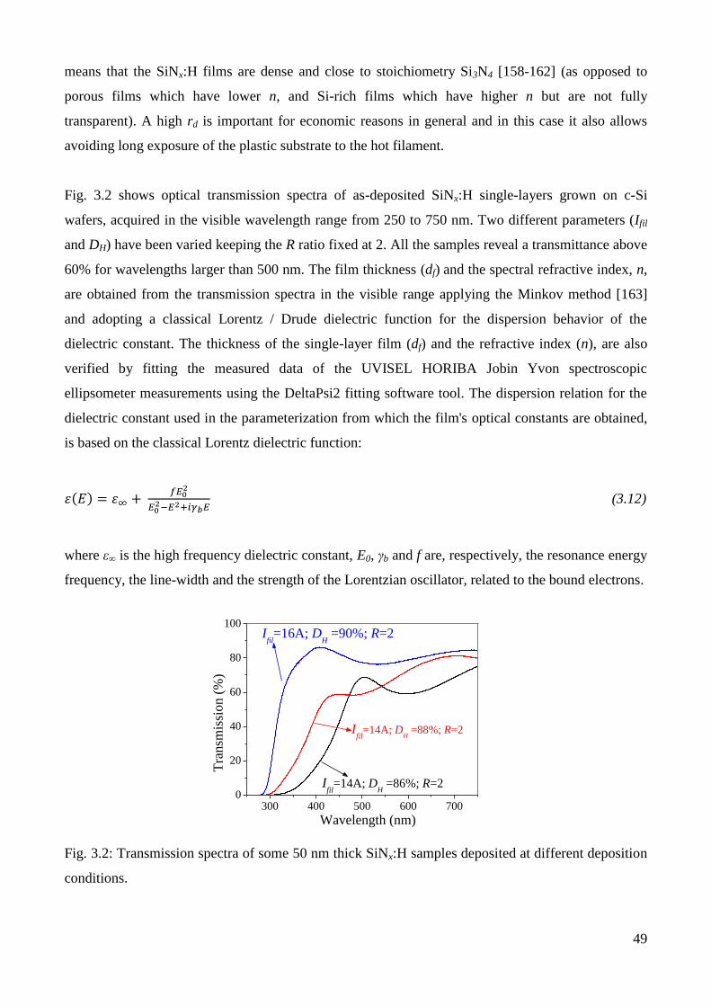
49
means that the SiNx:H films are dense and close to stoichiometry Si3N4 [158-162] (as opposed to
porous films which have lower n, and Si-rich films which have higher n but are not fully
transparent). A high rd is important for economic reasons in general and in this case it also allows
avoiding long exposure of the plastic substrate to the hot filament.
Fig. 3.2 shows optical transmission spectra of as-deposited SiNx:H single-layers grown on c-Si
wafers, acquired in the visible wavelength range from 250 to 750 nm. Two different parameters (Ifil
and DH) have been varied keeping the R ratio fixed at 2. All the samples reveal a transmittance above
60% for wavelengths larger than 500 nm. The film thickness (df) and the spectral refractive index, n,
are obtained from the transmission spectra in the visible range applying the Minkov method [163]
and adopting a classical Lorentz / Drude dielectric function for the dispersion behavior of the
dielectric constant. The thickness of the single-layer film (df) and the refractive index (n), are also
verified by fitting the measured data of the UVISEL HORIBA Jobin Yvon spectroscopic
ellipsometer measurements using the DeltaPsi2 fitting software tool. The dispersion relation for the
dielectric constant used in the parameterization from which the film's optical constants are obtained,
is based on the classical Lorentz dielectric function:
( ) = + 𝐸
2
𝐸 2 𝐸2 𝑖 𝐸
(3.12)
where ε∞ is the high frequency dielectric constant, E0, γb and f are, respectively, the resonance energy
frequency, the line-width and the strength of the Lorentzian oscillator, related to the bound electrons.
300 400 500 600 7000
20
40
60
80
100 I
fil=16A; D
H =90%; R=2
Wavelength (nm)
Tra
nsm
issi
on (
%)
Ifil
=14A; DH =86%; R=2
Ifil
=14A; DH =88%; R=2
Fig. 3.2: Transmission spectra of some 50 nm thick SiNx:H samples deposited at different deposition
conditions.

50
Fig. 3.3 shows the refractive index (n) of the SiNx:H single-layers as a function of ammonia-to-silane
gas flow rate ratio (R), for different H2 dilutions and filament currents (Ifil). Most of the films have n
>2 which is attributed to a Si-rich composition of the films. The refractive index approaches to the
stoichiometric value of 2 when R is increased from 2 to 3, when Ifil increases from 14 to 16 A, or
when H2 dilution increases from 86% (88% at R = 3) to 90%, keeping fixed all the other parameters.
1 2 3 4
1.9
2.0
2.1
2.2
2.3
2.4
2.5
I fil e
ffec
t
DH e
ffec
t
R effect
16 A, 88% DH
16 A, 90% DH
14 A, 88% DH
16 A, 86% DH
16 A, 88% DH
Ref
ract
ive
ind
ex,
n @
63
2.8
nm
R=F(NH3) / F(SiH
4)
16 A, 90% DH
14 A, 86% DH
Fig. 3.3: Refractive index, n for the different single-layers of SiNx:H, as a function of filament
current (Ifil), NH3 and SiH4 gas flow rate ratio (R) and hydrogen dilution (DH).
The above results are attributed to the effects of several mechanisms as discussed below:
When R increases, keeping all the other parameters fixed the amount of ammonia inside the
reactor increases and the decomposition probability of NH3 on the heated filament increases as
well. This effect increases the content of nitrogen and N/Si ratio inside the SiNx:H films; reaching
towards the stoichiometric value of refractive index (n~2) due to the increase of band gap and
can be explained by the Kramers-Kronig dispersion relation [164].
When Ifil increases, keeping all the other parameters fixed, the filament temperature increases as
well. This gives rise to higher order dissociation of source gases into radicals and thus increasing
the possibility of growing stoichiometric SiNx:H films.
When H2 dilution increases, keeping all the other parameters fixed, there are large number of H*
species to react with in the gas phase mechanism. Thus, the probability of abstraction reaction
increases as well, giving rise to a lower concentration of hydrogen inside the films and better
stoichiometry.
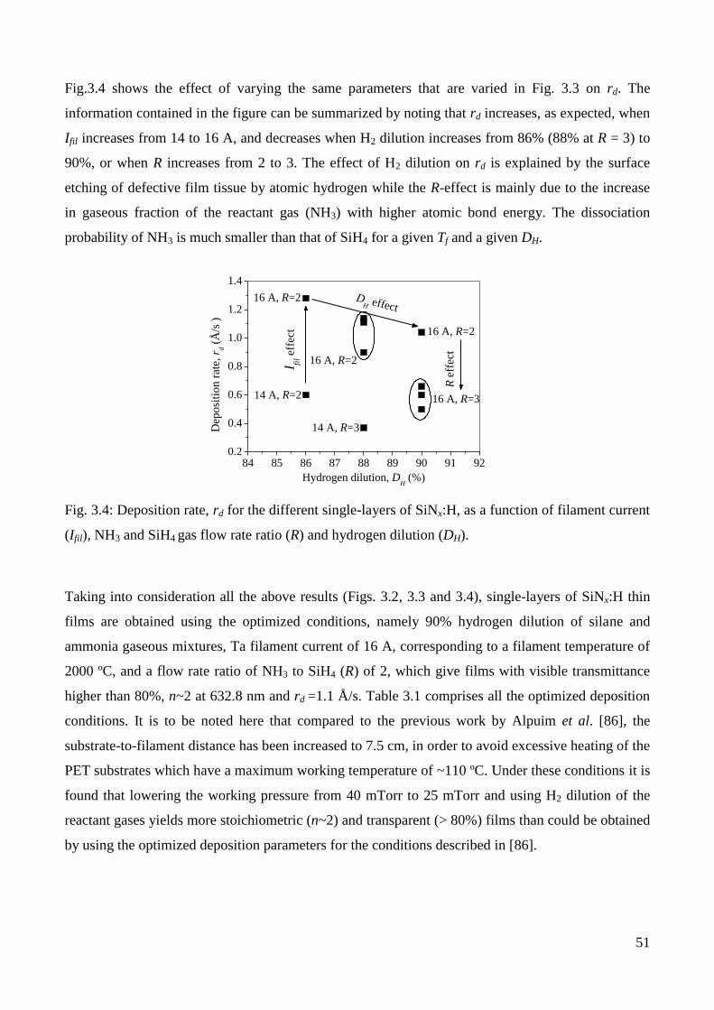
51
Fig.3.4 shows the effect of varying the same parameters that are varied in Fig. 3.3 on rd. The
information contained in the figure can be summarized by noting that rd increases, as expected, when
Ifil increases from 14 to 16 A, and decreases when H2 dilution increases from 86% (88% at R = 3) to
90%, or when R increases from 2 to 3. The effect of H2 dilution on rd is explained by the surface
etching of defective film tissue by atomic hydrogen while the R-effect is mainly due to the increase
in gaseous fraction of the reactant gas (NH3) with higher atomic bond energy. The dissociation
probability of NH3 is much smaller than that of SiH4 for a given Tf and a given DH.
84 85 86 87 88 89 90 91 920.2
0.4
0.6
0.8
1.0
1.2
1.4
R e
ffec
t
I fil e
ffec
tD
H effect
16 A, R=2
16 A, R=2
16 A, R=3
14 A, R=3
16 A, R=2
Dep
osi
tio
n r
ate,
rd (
Å/s
)
Hydrogen dilution, DH (%)
14 A, R=2
Fig. 3.4: Deposition rate, rd for the different single-layers of SiNx:H, as a function of filament current
(Ifil), NH3 and SiH4 gas flow rate ratio (R) and hydrogen dilution (DH).
Taking into consideration all the above results (Figs. 3.2, 3.3 and 3.4), single-layers of SiNx:H thin
films are obtained using the optimized conditions, namely 90% hydrogen dilution of silane and
ammonia gaseous mixtures, Ta filament current of 16 A, corresponding to a filament temperature of
2000 ºC, and a flow rate ratio of NH3 to SiH4 (R) of 2, which give films with visible transmittance
higher than 80%, n~2 at 632.8 nm and rd =1.1 Å/s. Table 3.1 comprises all the optimized deposition
conditions. It is to be noted here that compared to the previous work by Alpuim et al. [86], the
substrate-to-filament distance has been increased to 7.5 cm, in order to avoid excessive heating of the
PET substrates which have a maximum working temperature of ~110 ºC. Under these conditions it is
found that lowering the working pressure from 40 mTorr to 25 mTorr and using H2 dilution of the
reactant gases yields more stoichiometric (n~2) and transparent (> 80%) films than could be obtained
by using the optimized deposition parameters for the conditions described in [86].

52
Parameters Value
Maximum single-layer thickness (nm) 50-60
SiH4 flow rate F(SiH4) (sccm) 2
NH3 flow rate F(NH3) (sccm) 4
H2 flow rate F(H2) (sccm) 54
H2 dilution (DH) 90%
Process gas pressure pg (mTorr) 25
Nominal substrate temperature Ts (˚C) 100
Filament - substrate distance df-s (cm) 7.5
Filament temperature Tf (˚C) 2000
Electric current supplied to the filament (A) 16
Total filament surface area (cm2) 2.4
Table 3.1: Optimized deposition conditions for SiNx:H thin films using HW-CVD
The optimized SiNx:H thin films are characterized using different techniques. For the
characterizations with ellipsometry, XRD and X-ray reflectometry analysis, the films are deposited
on 510 µm thick c-Si wafers. For the optical transparency and morphological analysis and barrier
property measurements, the SiNx:H thin films are deposited on PET substrates. As mentioned earlier,
in order to avoid damage of the PET substrates due to the radiation heating from the glowing
filament, the single-layer film thickness is limited to 50-60 nm due to the increase of substrate
temperature with deposition time and irradiation from the glowing filament. The detailed
compositional analysis (FTIR, GD-OES and XPS measurements) of the films will be introduced in
chapter 4, where the as deposited films will be compared with the low energy plasma treated films.
3.5 CHARACTERISTICS OF OPTIMIZED SILICON NITRIDE SINGLE-LAYER FILMS:
3.5.1 Optical characteristics
Fig. 3.5 shows the reflectance (R) and the transmittance (T) spectra of the bare PET substrate and
SiNx:H films deposited on PET substrate with the above mentioned optimized deposition conditions.
The measurements are performed using Perkin Elmer Integrating Sphere apparatus both in
transmission and reflection modes. The T and R curves indicates that the SiNx:H layer is highly

53
transparent (> 80%) in the visible region, taking in to account the accuracy of the measurement (±1
%). It can also be seen from the spectrum that reflectance and transmittance of SiNx:H layer together
are around 100%, meaning that no absorption takes place in the layers and the films can perfectly be
used as a window layer for organic optoelectronic devices. The slight absorption below 450 nm is
due to the PET substrate itself.
350 400 450 500 550 600 650 700 750 800
0
20
40
60
80
100
Tra
nsm
itta
nce /
Refl
ecta
nce (
%)
Wavelength (nm)
T (PET + SiNx)
R (PET + SiNx)
T (PET)
R (PET)
Fig. 3.5: Reflection and transmission spectra of SiNx:H film on PET substrate. The reflectance (R)
and transmittance (T) of the layer together is almost 100%, means no absorption inside the films.
From the fit of the spectroscopic ellipsometric measured data to the model (equation 3.12), in the
visible region, the refractive index, n and the extinction coefficient, k, are obtained as shown in Fig.
3.6. The value of n at 632.8 nm is 2.01 which is close to the value 2.05 found in the literature for
stoichiometric amorphous Si3N4 [158-162]. The value of k shows that the film is not absorbing in the
visible region. The measured thickness of the single-layer is 50 ± 2 nm, which matches perfectly
with the initial thickness measurements by profilometer and XRR method (discussed later).
350 400 450 500 550 600 650 700 750 800
2.0
2.2
2.4
Refractive index
Extinction coefficient
Wavelength (nm)
Refr
acti
ve i
nd
ex
, n
0.0
0.1
0.2
Ex
tin
cti
on
co
eff
icie
nt,
k
Fig. 3.6: Refractive index (n) and extinction coefficient (k), in the visible region, obtained from the
ellipsometric measurement data for the single-layer of SiNx:H (50 nm) on c-Si substrate.
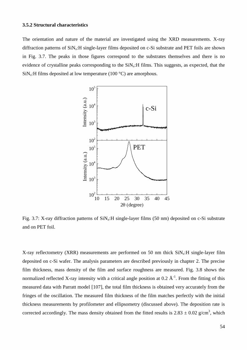
54
3.5.2 Structural characteristics
The orientation and nature of the material are investigated using the XRD measurements. X-ray
diffraction patterns of SiNx:H single-layer films deposited on c-Si substrate and PET foils are shown
in Fig. 3.7. The peaks in those figures correspond to the substrates themselves and there is no
evidence of crystalline peaks corresponding to the SiNx:H films. This suggests, as expected, that the
SiNx:H films deposited at low temperature (100 °C) are amorphous.
10 15 20 25 30 35 40 4510
2
103
104
105
102
103
104
105
Inte
nsi
ty (
a.u
.)
2(degree)
PET
Inte
nsi
ty (
a.u
.)
c-Si
Fig. 3.7: X-ray diffraction patterns of SiNx:H single-layer films (50 nm) deposited on c-Si substrate
and on PET foil.
X-ray reflectometry (XRR) measurements are performed on 50 nm thick SiNx:H single-layer film
deposited on c-Si wafer. The analysis parameters are described previously in chapter 2. The precise
film thickness, mass density of the film and surface roughness are measured. Fig. 3.8 shows the
normalized reflected X-ray intensity with a critical angle position at 0.2 Å-1
. From the fitting of this
measured data with Parratt model [107], the total film thickness is obtained very accurately from the
fringes of the oscillation. The measured film thickness of the film matches perfectly with the initial
thickness measurements by profilometer and ellipsometry (discussed above). The deposition rate is
corrected accordingly. The mass density obtained from the fitted results is 2.83 ± 0.02 g/cm3, which

55
is lower than that of stoichiometric Si3N4:H (3.1 g/cm3) reported in literature [158]. It is to be noted
here that compared to the previous work by Alpuim et al. [86] with mass density 2.56 g/cm3, using
H2 dilution of the source gases and increasing the filament to substrate distance (df-s) in the present
study, the mass density is higher. This is probably attributed to the effect of higher collisions of the
radicals between the filament and the substrate and the abstraction reaction of atomic hydrogen
during the surface reactions as discussed before in this chapter. The surface roughness of the film is 2
nm and is comparable to the AFM measurement (2.1 nm).
0.04 0.06 0.08 0.10 0.12 0.14 0.16
Norm
aliz
ed i
nte
nsi
ty, I/
I 0
q (Å-1)
Fig. 3.8: X-ray reflectivity signal for the 50 nm thick SiNx:H single-layer deposited on c-Si wafer.
3.5.3 Morphological characteristics
The average surface roughness of the single-layer SiNx:H thin films is analysed using the tapping
mode AFM technique. The single-layers are deposited on PET substrates at Ts =100 °C. It should be
noted here that the initial roughness of the PET substrate depends considerably on the cleaning of
dust particles by different solvents (possibly due to the wettability of PET towards those solvents).
Several cleaning methods are undertaken in order to find an optimized method which gives rise to
minimum initial roughness, as shown in Table 3.2. The minimum initial average roughness for PET
foils before being exposed to HW-CVD process is 1.35 ± 0.06 nm which corresponds to a cleaning
procedure of rinsing with DI water in an ultrasonic bath for 15 s. The average roughness of the bare
PET substrate after exposure to the hot filament for the same time (400 s) as it takes for one single-
layer (50 nm) deposition, but without film growth, is around 55 nm. The roughness of PET increases
strongly when the PET foil is exposed to the Ta filament, probably due to the fact that the glass
transition of PET at around 80 °C is somewhat overcome (100 °C) inducing a warping of the foil.
This explains the high initial roughness of the SiNx:H single-layer films deposited on PET substrates
(discussed in next paragraph).

56
Cleaning
method
0 s in
ultrasonic
15 s in
ultrasonic
60 s in
ultrasonic
300 s in
ultrasonic
600 s in
ultrasonic
Deionized
water
4.06 nm 1.35 nm 9 nm 9.45 nm 14.8 nm
Isopropyl
alcohol
8.17 nm 2.16 nm 8.2 nm 9.89 nm 16 nm
Acetone 8.83 nm 3 nm 10.3 nm 10.56 nm 17.8 nm
Table 3.2: Initial average surface roughness of the bare PET substrates with different cleaning
methods.
Three dimensional surface images of the single-layers with increasing thickness are shown in Fig.
3.9 and summarized in Fig. 3.10. Fig. 3.10 shows the decrease in average surface roughness from 55
nm to 23 nm when the PET substrate is covered by a SiNx:H layer of thickness at least equal to a
critical thickness (dc) of 50 nm. Critical thickness in this case is the maximum single-layer thickness
which can be deposited in a single run inside the HW-CVD reactor without damaging the PET
substrate and produces the maximum average surface roughness reduction. From this initial result of
average roughness reduction, it is expected that the permeation of water vapor will be reduced
maximum, when the substrate is coated with a layer thickness near its critical thickness value (50
nm).
(a) (b)

57
(c) (d)
(e) (f)
Fig. 3.9: Three dimensional AFM images of the surfaces of SiNx:H single-layers deposited on PET
substrates with increasing thickness: (a) 10 nm, (b) 20 nm, (c) 30 nm, (d) 40 nm, (e) 50 nm and (f) 60
nm. [To observe the effect, the sensitivity of the color scale is increased].
0 10 20 30 40 50 60 70
20
30
40
50
60
70
Roughnes
s, R
avg
. (nm
)
Single-layer coating thickness, df (nm)
dc
Fig. 3.10: Variation of average roughness of SiNx:H single-layers coated on PET substrates with the
coating thickness.

58
3.5.4 Barrier characteristics of single-layer films
The permeation barrier properties of the single-layer SiNx:H films deposited on PET substrates are
performed using the electrical calcium degradation test method at ambient atmospheric conditions.
Figure 3.11 (a) shows the evolution of normalized conductance of Ca sensors, deposited on PET
substrates whose back side has been coated with SiNx:H single-layers with thickness ranging from 10
nm to 60 nm. Bare plastic is used as the reference for the calcium degradation test. With the increase
of the SiNx:H single-layer thickness (df), the minimum time taken by the water molecules to
permeate through the whole barrier thickness including PET substrate (“lag-time”), is increased as
can be seen in Fig. 3.11 (b). As seen in Fig. 3.11 (c), the barrier performance assessed by the
decrease of the WVTR value also improves with the increase of SiNx:H single-layer coating
thickness (df). The WVTR of the single-layers depends strongly on the surface roughness of the films
[165] and varies in a similar way with the average roughness variation as expected. The curve can be
divided into three regions. The first one, from 0 to 20 nm, corresponds to the “threshold thickness
(dth)” region, below which there is no barrier effect and over which (df >dth, defining the second
region) the permeation rate drops steeply until it stabilizes at a critical thickness (dc) value (about 50
to 60 nm in this case, defining the third region). It should be noted that evolution of WVTR versus
the single-layer thickness (Fig. 3.11 (c)) follows the same trend as the evolution of surface roughness
versus thickness (Fig. 3.10). For df >dc, no further significant decrease in WVTR is observed, the
stabilized value being ~1 × 10⁻²
g/ m2.day. From this first measurement, we define the critical
thickness as the maximum single-layer thickness resulting in the maximum WVTR reduction.
It is worth mentioning that the critical thickness (dc) for HW-CVD grown SiNx:H single-layer thin
films falls in the same range (50 to 100 nm) as reported by several authors [18, 68, 71, 166-168]. The
dc value depends considerably on the deposition method. The above results can be interpreted taking
into account the gas permeation mechanism through the thin films, as described by H. Chatham
[166]. In the second region of Fig. 3.11 (c), where permeation rate decreases with thickness, is
dominated by the thermally activated diffusion of water vapor through the films. In this region the
permeation rate varies inversely with the coating thickness (df) and the total permeation through the
barrier coated polymer substrates can be expressed following a parallel type equation (3.13) [71,
169]:
=
+
𝑠
𝑠 (3.13)

59
Where dtotal, df and ds are total thickness of the structure, coating thickness and substrate thickness
respectively. Ptotal, Pf and Ps are overall permeability of the structure, permeability of the coating and
permeability of the substrate respectively.
This is followed by the defect dominated permeation region, where the permeation rate is
independent of the coating thickness (df). It should be noted that the samples are deposited on a face-
down sample holder in the HW-CVD system. Therefore, the probability of defect formation due to
the inner wall flakes is small. Takeda and co-workers [167, 170, 171] and Leterrier et al. [71] found
that, with the increase of coating thickness, the compressive stresses are lowered. This indicates a
stress relaxation process during the film growth which in turns results in the formation of nano-
scopic defects. As discussed in chapter 1, the diffusion of water molecules is largely controlled by
the nano-scopic defects and thus after the critical thickness no more barrier improvement is observed
up to a definite range. Therefore, this proves that the permeation rate for single-layer barriers on
polymer substrates generally changes by no more than one order of magnitude for the normal CVD
deposited thin films and thus a single-layer barrier coating alone is not effective in reducing the
overall barrier properties down to the required barrier for utilization of organic optoelectronic
devices.
Based only on these WVTR results; it is expected that the stack of several SiNx:H single-layers, each
having a thickness equal to or greater than the critical thickness (dc), will be very effective in
reducing the overall WVTR value and thereby in improving the overall performance of the
permeation barrier. This is due to the independence of structural defects during the subsequent
deposited single-layers.
0 2 4 6 8 10 12 140.0
0.2
0.4
0.6
0.8
1.0
Norm
aliz
ed C
onduct
ance
(S
)
Time (h)
Bare PET
10 nm
20 nm
30 nm
40 nm
50 nm
60 nm
0 10 20 30 40 50 60 700
1
2
3
4
5
Lag
-tim
e (h
)
Single-layer coating thickness, df (nm)
(a) (b)
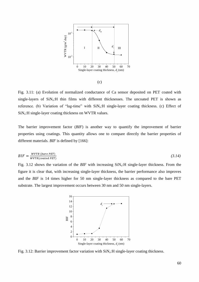
60
0 10 20 30 40 50 60 70
10-2
10-1
IIIII
WV
TR
(g
/m2.d
ay)
Single-layer coating thickness, df (nm)
I
dth
dc
(c)
Fig. 3.11: (a) Evolution of normalized conductance of Ca sensor deposited on PET coated with
single-layers of SiNx:H thin films with different thicknesses. The uncoated PET is shown as
reference. (b) Variation of “lag-time” with SiNx:H single-layer coating thickness. (c) Effect of
SiNx:H single-layer coating thickness on WVTR values.
The barrier improvement factor (BIF) is another way to quantify the improvement of barrier
properties using coatings. This quantity allows one to compare directly the barrier properties of
different materials. BIF is defined by [166]:
= ( 𝑟 𝐸 )
(𝑐 𝐸 ) (3.14)
Fig. 3.12 shows the variation of the BIF with increasing SiNx:H single-layer thickness. From the
figure it is clear that, with increasing single-layer thickness, the barrier performance also improves
and the BIF is 14 times higher for 50 nm single-layer thickness as compared to the bare PET
substrate. The largest improvement occurs between 30 nm and 50 nm single-layers.
0 10 20 30 40 50 60 700
2
4
6
8
10
12
14
16
BIF
Single-layer coating thickness, df (nm)
dc
Fig. 3.12: Barrier improvement factor variation with SiNx:H single-layer coating thickness.
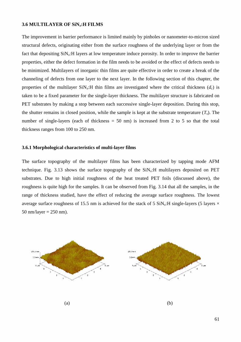
61
3.6 MULTILAYER OF SiNx:H FILMS
The improvement in barrier performance is limited mainly by pinholes or nanometer-to-micron sized
structural defects, originating either from the surface roughness of the underlying layer or from the
fact that depositing SiNx:H layers at low temperature induce porosity. In order to improve the barrier
properties, either the defect formation in the film needs to be avoided or the effect of defects needs to
be minimized. Multilayers of inorganic thin films are quite effective in order to create a break of the
channeling of defects from one layer to the next layer. In the following section of this chapter, the
properties of the multilayer SiNx:H thin films are investigated where the critical thickness (dc) is
taken to be a fixed parameter for the single-layer thickness. The multilayer structure is fabricated on
PET substrates by making a stop between each successive single-layer deposition. During this stop,
the shutter remains in closed position, while the sample is kept at the substrate temperature (Ts). The
number of single-layers (each of thickness = 50 nm) is increased from 2 to 5 so that the total
thickness ranges from 100 to 250 nm.
3.6.1 Morphological characteristics of multi-layer films
The surface topography of the multilayer films has been characterized by tapping mode AFM
technique. Fig. 3.13 shows the surface topography of the SiNx:H multilayers deposited on PET
substrates. Due to high initial roughness of the heat treated PET foils (discussed above), the
roughness is quite high for the samples. It can be observed from Fig. 3.14 that all the samples, in the
range of thickness studied, have the effect of reducing the average surface roughness. The lowest
average surface roughness of 15.5 nm is achieved for the stack of 5 SiNx:H single-layers (5 layers ×
50 nm/layer = 250 nm).
(a) (b)

62
(c) (d)
Fig. 3.13: Three dimensional AFM images of the surfaces of SiNx:H multi-layers deposited on PET
substrates with increasing thickness: (a) 50 nm + 50 nm, (b) 50 nm + 50 nm + 50 nm, (c) 50 nm + 50
nm + 50 nm + 50 nm, (d) 50 nm + 50 nm + 50 nm + 50 nm + 50 nm. [To observe the effect, the
sensitivity of the color scale is increased].
50 100 150 200 250 30010
15
20
25
30
Ro
ug
hn
ess
Ra
vg. (
nm
)
Multilayer thickness (nm)
Fig. 3.14: Variation of average roughness of SiNx:H multi-layers coated on PET substrates with the
coating thickness.
3.6.2 Barrier characteristics of multi-layer films
The evolutions of normalized conductance of the Ca sensors deposited on such multi-barrier coated
PET substrates are shown in Fig. 3.15 (a). Slight kinks are observable in the traces, which are
probably due to the inhomogeneous oxidation of the calcium surface. One possible reason of this
inhomogeneous oxidation is the in-homogeneities inside both the barrier layers and the PET
substrate. When the number of SiNx:H single layers increases, the number of interfaces between
SiNx:H films increases as well and there are possible breaks of the propagation of pinholes from one
single-layer to the next single-layer. Due to that reason and to the increase in total thickness of the
coating, the minimum time taken by the water molecules to reach the Ca sensor, which is at the

63
opposite side of the coated PET substrates (“lag-time”), increases with increasing number of stacked
SiNx:H single-layers as shown in Fig. 3.15 (b). A maximum lag-time of 14 hours has been achieved
with 5 stacked SiNx:H single-layers. The WVTR values have also decreased monotonically with
increasing number of layers (see Fig. 3.15 (c)), reaching a minimum value of ~7.9 × 10⁻³
g/ (m2.day).
Fig. 3.15 (d) shows the variation of BIF with increasing number of SiNx:H multi-layer thickness.
When the single-layers of SiNx:H are stacked, the BIF increases monotonically as compared to the
bare PET substrates and reaches to the value of 21. This trend suggests that, if the number of layers is
further increased, the barrier properties will improve. But the increased thickness will decrease the
optical transparency and the mechanical flexibility of the whole structure. Thus a trade-off should be
found.
The above observations are consistent as expected. The multilayer structures improve the barrier
properties to some extent; however, the improvement is not sufficient in terms of the encapsulation
requirements. There are two factors that affect the whole barrier mechanism for the multilayer
structures. First of all, the surface quality of the individual inorganic films is quite critical in order to
improve the permeation property. The interface roughness should be as small as possible in order to
deposit the subsequent inorganic layer with higher structural quality. Secondly, the probability of the
occurrence of pinholes or structural defects at the same lateral position in two subsequent thin films
is not zero. This may facilitate the diffusion of water molecules in a faster way. In order to improve
the overall barrier property, the film surface property should be modified. In the following chapter
we will focus our efforts to modify the interface properties using impact of low energy ions.
0 10 20 30 40 500.0
0.2
0.4
0.6
0.8
1.0
No
rmal
ized
Co
nd
uct
ance
(S
)
Time (h)
50+50
50+50+50
50+50+50+50
50+50+50+50+50
50 100 150 200 250 3000
5
10
15
20
Lag
-tim
e (h
)
Multilayer thickness (nm)
(a) (b)

64
50 100 150 200 250 300
8x10⁻³
9x10⁻³
10-2
WV
TR
(g
/m2.d
ay)
Multilayer thickness (nm)
50 100 150 200 250 3000
5
10
15
20
25
BIF
Multilayer thickness (nm)
(c) (d)
Fig. 3.15: (a) Evolution of normalized conductance of Ca sensor deposited on PET coated with
multi-layers of SiNx:H thin films with different thicknesses. (b) Variation of “lag-time” with SiNx:H
multi-layer coating thickness. (c) Effect of SiNx:H multi-layer coating thickness on WVTR values.
(d) Barrier improvement factor variation with SiNx:H multi-layer coating thickness.
3.6 SUMMARY OF CHAPTER 3
i. In this chapter, using the HW-CVD technique, based on silane and ammonia gaseous mixtures
diluted in hydrogen at a substrate temperature of 100 °C and after an optimization taking into
account the different growth parameters, we have deposited device quality transparent and
stoichiometric silicon nitride thin films which can be used as moisture barrier layers for
encapsulation of flexible organic electronic devices.
ii. The optimized SiNx:H thin films are characterized using different techniques. Transmission
measurements suggest that the films are highly transparent in the visible region. The refractive
index measurement indicates that the films are close to the stoichiometric Si3N4. The amorphous
nature of the low temperature deposited films is evidenced by XRD analysis. The density
measurements carried out by XRR method informs about the mass density value of the films.
iii. A critical thickness is defined from the initial roughness measurements by AFM and this value is
confirmed by the permeation barrier measurements using the electrical calcium test. A tentative
physical interpretation is given taking into account the gas permeation mechanism through films
and model described previously by different authors.
iv. In order to improve the permeation barrier property, multilayers of SiNx:H films are used to
create a break in the propagation of defects throughout the whole structure. Although, the

65
multilayer structure improves the barrier property to some extent, however, the WVTR value is
quite high to fulfil the requirement for the organic optoelectronic devices.

66
CHAPTER 4
SILICON NITRIDE MULTILAYER TREATED BY ARGON
PLASMA
4.1 INTRODUCTION
The improvement of the barrier properties is mainly limited by the pinholes or defects that propagate
from one single-layer to the other. The multilayer stack of SiNx:H single-layers logically induces a
barrier improvement compared to the single-layer films. However, the barrier properties (WVTR) of
the multilayer stacks are several order of magnitude higher compared to the targeted values. As
discussed in the previous chapter, this limited improvement is due to the non-zero probability of
occurrence of pinholes or structural defects crossing subsequent SiNx:H single-layers. Therefore, in
the thesis, we looked for a technique which could drastically modify the surface structure of each
single-layer films near the interface without modifying significantly the bulk layer structure, which is
challenging. The conventional techniques to reduce the effect of pinhole or defect propagation are
based on developing alternating hybrid layer structures, which could reduce the permeation rate
substantially. This route seems interesting if we are able to deposit the organic layers as well as the
inorganic layers in the same reactor, which is not our case. In this thesis, the effect of ion treatment
on the single-layer surfaces on the overall permeation barrier properties has been studied. This
unique encapsulation method is based on low energy ion bombardment on the thin film surface to
create atomic displacements at the surface and then stacking the single-layer films one after the other
to develop a multilayer structure.
The plasma treatment is a well-known industrial process used to deposit or to etch materials and to
modify the film surface properties for various commercial purposes. The use of plasma surface
treatment in corrosion resistant coating technology is already a well-established technique. Most of
these treatment methods are based on plasma produced by corona or glow discharges. The basic aim
of this chapter is to deal with the plasma treatment parameters in which the plasma active species
interact only very superficially with the thin film material, i.e. with the first few atomic layers of the
surface of the thin films. This interaction can lead to significant modifications of the film surfaces
which could be beneficial for the diffusion barrier purposes. The idea of such plasma treatment is not
to use highly energetic ions. It should neither damage the surface or the bulk layer of the films, nor
67
inject ions or atoms below the surface (ion implantation), nor remove material from the film
(sputtering or etching) [172].
4.2 PLASMA TREATMENT PROCEDURE
In order to study the effects of plasma ion bombardment on the film surface, the ion bombardment
parameters, such as, ion type, ion kinetic energy and ion flux (number of ions impinging per unit area
of the electrode per unit time), need to be well controlled. In a plasma generator system, ions can
have a considerable amount of kinetic energy compared to the neutrals because the ions can gain
energy when they are accelerated inside the electric field produced in the plasma sheaths (as
discussed later) between the two electrodes. Due to this reason, ions can induce film surface
treatment or modify the film surface in comparison to the neutrals [172]. In the following we
consider only cold (non-local thermodynamic equilibrium) plasmas where the energy of the electrons
(Te) is much higher than the energy of the ions.
Among the various types of plasma treatment methods, the radio frequency (RF) PE-CVD is widely
used in laboratories. The details of the RF PE-CVD system are described in Chapter 2. It is a
capacitive-coupled PE-CVD system, where the RF power is fed to the bottom electrode (anode) and
top electrode (cathode) is used as a substrate holder. The plasma is produced between the two
electrodes due to the inelastic collisions of electrons having energy above some threshold energy
with the neutral species [172-175]. Plasma electron density n0 and the electron temperature Te are the
fundamental properties of the plasma. In a typical low pressure capacitively-coupled RF PE-CVD
cold plasma system, the plasma electrons having a non-Maxwellian (Druyvesteyn) energy
distribution, defines the electron temperature, Te [173]:
𝑁( ) =
( 𝑒) /2 [− (
𝐸
𝑒)2
] (4.1)
Where, A and B are constants depending on the energy distribution. The neutral species are ionized
due to the collisions with the energetic electrons according to the convolution
𝑁𝑖 = ∫𝑛0( )𝑓𝑖( ) (4.2)
Where, fi is the ionization probability as shown schematically in Fig. 4.1.
The electrons have a higher mobility compared to the positive ions in an ionized gas, however inside
the plasma where collective behavior of charged particles is dominant; a plasma sheath is created
next to the electrodes due to quasi-neutrality conditions [173]. The plasma sheath acts as a diode and
the electrodes acquire a self-bias voltage. The bias voltage is divided between the two electrodes and

68
inversely proportional to the electrode areas. Thus the smaller electrode acquires the larger bias
voltage. The sheath voltage (roughly the bias voltage) accelerates the positive ions and the ions gain
kinetic energies in order to bombard the sample. If the mean free path of the ions between two
successive collisions is higher than the sheath thickness, then the mean ion energy is just: ion charge
× VBias. If conversely the mean free path of ions is smaller than the space charge sheath then the mean
ion energy is a fraction of that, say 0.4 [174, 176, 177]. At a typical low pressure region (say 50
mTorr), there are still significant ion collisions in the sheath. Therefore, a wide ion energy
distribution occurs (Fig. 4.2), where the maximum energy Emax (i.e. the sheath voltage) is above the
mean ion energy (Ēion) [176, 177]. In a simple capacitive coupled PE-CVD system, VBias is
proportional to the RF power and inversely proportional to the working pressure. The ion current and
ion energy both vary with the input RF power (PRF). The ion current increases with the square-root
of both RF power and working pressure [173]. One useful approximate formula to calculate the ion
current is Iion ≈ PRF / VBias. In the rest of this chapter, the results are discussed in terms of power
density (Pw = PRF / electrode area) and working pressure (pg). However, it should be noted that the
values of power density and working pressure only reflect the maximum ion energy (Emax) whereas
the mean ion energy is 0.4 times of Emax. The ion flux, Fi, is defined as the total current falling on the
electrode area [172, 173]
𝑖 = 𝑖
𝑒 𝑒 𝑟 𝑒 (ions/m
2.s) (4.3)
The ion fluence is an important parameter for the plasma treatment which can affect considerably for
constant ion energy and defined as the product of the ion flux by treatment duration (t) [172, 173].
Ion fluence = Fion × t (ions.m-2
) (4.4)
The ion energy fluence is the other important parameter which is defined as the product of ion
fluence by kinetic energy of each ions impinging on the cathode surface:
Ion energy fluence = Ion fluence × Emax (eV/m2) (4.5)

69
Fig. 4.1: Schematic diagram of electron temperature Te and the ionization probability of a species.
Fig. 4.2: An example of typical ion energy distribution in conventional plasma deposition at 5 Pa
pressure. Reprinted from [174] with permission from 2002 Elsevier.
Ions being accelerated by the cathode sheath potential gain sufficient energy with the maximum
energy impinging the cathode surface corresponding to the bias potential. Such ions striking a
material can penetrate to a certain depth within a depth distribution [178]. The depth distribution
depends on the nature of the ions, their energy and their atomic mass and on the density and the
atomic mass of target atoms. During their travel through the material, energy is transferred to the
near environment. Depending on the energy range, ions can transfer energy in a pure mechanical way
through nuclear interaction (nuclear stopping power), but can also loose energy through electronic
collisions (electronic stopping power). In the low energy range (below 50 eV) these mechanisms will
cause rearrangement of the neighboring atoms, initiating an atomic collision cascade [179]. As a
result, target atoms will be relocated from their original position. Ions (mass M1) striking elastically

70
the atoms at the surface of the film transfer energy to the target atoms (mass M2). The maximum
energy transfer (ET) from an ion of maximum energy, Emax, to an atom at rest is obtained from the
laws of conservation of energy and momentum and is given by [180]
= 2
( 2)2 (4.6)
There is some minimum energy that must be transferred in order to produce atomic displacement,
called the displacement threshold energy, Ed. By definition of Ed, the probability of displacement for
ET < Ed is zero. If Ed is a fixed value under all conditions then the probability of displacement for ET
> Ed is one. The struck lattice atom with energy at least ET is referred as primary knock-on atom.
This atom moves through the lattice producing energy transfer to the neighboring atoms, resulting in
a collision cascade mechanism [181]. The cohesive energy of a crystal is defined as the energy which
must be added to the crystal in order to separate its components into neutral free atoms at rest, at
infinite separation, with the same electronic configuration. It is known that the typical cohesive
energy between atoms in a solid equals several eV (~4.6 eV for Si atoms) [182]. Whenever the
impinging ions have sufficient energy, they can displace atoms in the lattice. The typical values for
average surface atomic displacement threshold energy for Si (atomic mass = 28 amu) are roughly in
the range of ~15 to 25 eV and ~20 to 40 eV for more bonded bulk atom displacement [183-186].
When the ions have higher kinetic energy, the target atoms are sputtered away. The sputtering energy
threshold for Si is roughly >50 eV and sputter yield increases with the increasing incoming ion
energy [180, 187]. The energy threshold values for N atoms are slightly larger than Si atoms, due to
the lower energy transfer from the ions toward N atoms owing to its lower atomic mass (atomic mass
= 14 amu) and to its higher cohesive energy. The ion bombardment on the surface must be such that
it disrupts the atomic distribution to a few nm in depth, disturbing the continuity of a structural defect
through this interface but it cannot significantly damage the interface.
The plasma treatment is carried out between each successive SiNx:H single-layer deposition by
moving the sample holder from HW-CVD chamber to the RF PE-CVD chamber through the gate
valve without breaking the vacuum keeping the same substrate temperature (100 °C). The number of
plasma treated single-layers (m) is increased by stacking the layers one after the other and thus
increase the total thickness of the barrier. For the plasma treatment argon (atomic mass = 40 amu and
first ionization potential = 15.75 eV) has been chosen as an ion source for bombarding the sample
surface at normal incidence, because as being one of the rare gases, it is much less reactive than
oxygen ions for example. Ar is a good compromise in terms of ionization energy (15.75 eV) between
higher atomic number rare gases (like Kr and Xe) and lower atomic number rare gases (like He and
Ne) for displacing Si atoms according to equation 4.6. Four different parameters are varied in order

71
to obtain an optimal treatment condition which can improve the barrier properties significantly. The
following block diagram shows the variation of treatment parameters: treatment time (t); power
density (Pw); working pressure (pg) and number of layers (m). Here the thickness of each single-layer
is fixed at the critical thickness (50 nm). The sub-script b stands for the ‘best’ parameter while others
remain fixed, which gives rise to the ‘best’ barrier properties under such conditions. It should be
reminded that the four parameters are not totally independent to each other. Thus, best parameter
does not mean necessarily the optimum value versus variation of each parameter.
The treatment parameters are optimized using a double layer SiNx:H structure (total thickness = 100
nm), in order to simplify the procedure. First, the treatment duration is optimized with a fixed power
density and working pressure. This is followed by variation of power density and working pressure
in order to find an optimum treatment parameter while the treatment duration remains constant.
Whenever one parameter is varied, other parameters remain fixed. Finally, all the observations are
taken into account to obtain good barrier properties by increasing the total number of layers.
In order to observe effects on the permeation barrier properties due to the different plasma treatment
parameters, and to give a coherent physical interpretation of the experimental results, intermediate
steps including extra analytical techniques have been mandatory through new specific samples
prepared for this purpose. For example, morphological, compositional and structural data demanded
extra samples deposited on c-Si substrates in order to be assessed through AFM, Fourier Transform
Infrared Spectroscopy, Glow Discharge Optical Emission Spectroscopy, X- ray Photoelectron
Spectroscopy and X-ray Reflectometry measurements. These intermediate steps have been possible
with the help of INL at Braga; LPMC at Ecole Polytechnique; IRAMIS-CEA Saclay and HORIBA
Jobin-Yvon at Palaiseau.
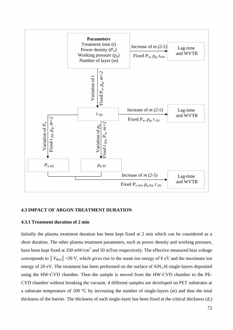
72
4.3 IMPACT OF ARGON TREATMENT DURATION
4.3.1 Treatment duration of 2 min
Initially the plasma treatment duration has been kept fixed at 2 min which can be considered as a
short duration. The other plasma treatment parameters, such as power density and working pressure,
have been kept fixed at 350 mW/cm2 and 50 mTorr respectively. The effective measured bias voltage
corresponds to VBias=20 V, which gives rise to the mean ion energy of 8 eV and the maximum ion
energy of 20 eV. The treatment has been performed on the surface of SiNx:H single-layers deposited
using the HW-CVD chamber. Then the sample is moved from the HW-CVD chamber to the PE-
CVD chamber without breaking the vacuum. 4 different samples are developed on PET substrates at
a substrate temperature of 100 °C by increasing the number of single-layers (m) and thus the total
thickness of the barrier. The thickness of each single-layer has been fixed at the critical thickness (dc)
Parameters
Treatment time (t)
Power density (Pw)
Working pressure (pg)
Number of layer (m)
t (b)
Lag-time
and WVTR
pg (b)
Pw (b)
Lag-time
and WVTR
Lag-time
and WVTR
Var
iati
on o
f t
Fix
ed P
w, p
g, m
=2
F
ixed
t (
b), P
w, m
=2
Fix
ed t
(b
), p
g, m
=2
Var
iati
on o
f P
w
Var
iati
on o
f p
g
Increase of m (2-5)
Fixed Pw, pg, tmin
Fixed Pw, pg, t (b)
Increase of m (2-5)
Increase of m (2-5)
Fixed Pw (b), pg (b), t (b)

73
of 50 nm and the developed samples are multiple of m × 50 nm, where m varies from 2 to 5. The
effect of plasma treatment is investigated by assessing their surface roughness by tapping mode AFM
method and their barrier properties (lag-time and WVTR) by electrical calcium degradation tests.
4.3.1.1 Morphological effect
The three dimensional surface images of the multilayers are shown in Fig. 4.3 and summarized in
Fig. 4.4. The high initial roughness of the samples corresponds to the very high initial roughness of
the PET substrates when heat treated as discussed before. It should be reminded that the high initial
roughness of PET is decreased drastically when it is coated by 50 nm SiNx:H single-layer (see
Chapter 3). The constant average surface roughness values of the multilayers shows that there is
almost no significant effect of the plasma treatment on the surface of the SiNx:H layers with such
treatment conditions and short treatment time of 2 min.
(a) (b)
(c) (d)
Fig. 4.3: Three dimensional AFM images of the surfaces of SiNx:H multi-layers deposited on PET
substrates with 2 min Ar plasma surface treatment time performed between each single-layer

74
deposition: (a) 50 nm + 50 nm, (b) 50 nm + 50 nm + 50 nm, (c) 50 nm + 50 nm + 50 nm + 50 nm, (d)
50 nm + 50 nm + 50 nm + 50 nm + 50 nm.
50 100 150 200 250 30010
20
30
40
50
Ro
ug
hn
ess
Ravg
. (n
m)
Multilayer thickness (nm)
Fig. 4.4: Average surface roughness of SiNx:H multi-layers deposited on PET substrates treated by
Ar plasma during 2 min between each single-layer deposition.
4.3.1.2 Barrier effect
Fig. 4.5 (a) shows the evolutions of normalized conductance for the calcium sensors deposited on the
barrier coated PET substrates. The number of layers (m) is increased from 2 to 5 and thus the total
barrier thickness increases from 100 nm to 250 nm, where the thickness of each single-layer is fixed
at 50 nm and the argon plasma treatment has been performed between each subsequent single-layer
deposition with the above mentioned conditions. With the increase of the number of layers, the
minimum time taken by the water molecules to penetrate through the whole thickness (barrier +
substrate) increases, as seen from the lag-time variation with multilayer thickness in Fig. 4.5 (b). The
lag-time variation for the multilayers without any argon treatment (discussed in previous chapter) is
shown for comparison. It can be clearly observed that with the plasma treatment for a short duration,
the lag-time increases and reaches a maximum value of 17 h for 5 stacked single-layers (total
thickness =250 nm). The WVTR also varies with the number of layers as shown in Fig. 4.5 (c).
There is a slight decrease of WVTR value (~11.4%) compared to the multilayers without any argon
plasma treatment. The minimum WVTR value with such treatment conditions and using 5 stacked
single-layers is 7 ×10⁻³
g/m2.day. However, even though the plasma treatment reduces the effective
WVTR slightly, the minimum WVTR value obtained with such conditions is not sufficient for the
targeted value. In order to reduce the WVTR further, several other parameters should be varied. The
argon plasma treatment duration will be increased in the next section using a minimum number of
stacked single-layers (m =2, total thickness ≈ 100 nm).

75
0 20 40 60 80 1000.0
0.2
0.4
0.6
0.8
1.0N
orm
aliz
ed C
on
du
ctan
ce (
S)
Time (h)
50+Ar+50
50+Ar+50+Ar+50
50+Ar+50+Ar+50+Ar+50
50+Ar+50+Ar+50+Ar+50+Ar+50
50 100 150 200 250 3000
5
10
15
20
25
Lag
-tim
e (h
)
Multilayer thickness, d (nm)
Lag-time (without Ar treatment)
Lag-time (with Ar treatment)
(a) (b)
50 100 150 200 250 3000.005
0.01
0.015
WV
TR
(g
/m2.d
ay)
Multilayer thickness, d (nm)
WVTR (without Ar treatment)
WVTR (with Ar treatment)
(c)
Fig. 4.5: (a) Normalised conductance of Ca sensors deposited on barrier coated PET substrates
versus time for SiNx:H multi-layers separated by 2 min Ar plasma surface treatment. (b) Evolution of
the “lag-time” versus the SiNx:H multi-layer thickness. (c) Evolution of WVTR values versus the
SiNx:H multi-layer thickness. The evolutions of lag-time and WVTR for the SiNx:H multi-layers
without any Ar plasma treatment are shown for comparison.
4.3.2 Variation of treatment duration for double-layer
The argon plasma treatment duration has been increased from 2 min until 15 min (2, 5, 8, 10 and 15
min) in order to investigate the impact on the overall barrier properties. The power density and
working pressure have been kept fixed at 350 mW/cm2 and 50 mTorr as mentioned above. The
measurements have been carried out on double-layer structures in order to simplify both the
deposition process for all the concerned samples and the subsequent interpretations. The total
thickness of the double-layer structures being 100 nm (2 × 50 nm), the plasma treatment has been

76
carried out once after depositing the first single-layer. It should be noted that with the increase of the
treatment duration, the ion fluence increases as well, as shown in Table 4.1.
Power
density, Pw
(mW/cm2)
Pressure,
pg
(mTorr)
VBias
(V)
Maximum
ion energy
(eV)
Time,
t
(s)
Ion flux,
Fi
(cm-2
.s-1
)
Ion fluence
(cm-2
)
Ion energy
fluence
(eV. cm-2
)
350 50 -20 20 120 1.1 × 10¹⁷
13 × 1018
26 × 1019
350 50 -20 20 300 1.1 × 10¹⁷
33 × 1018
66 × 1019
350 50 -20 20 480 1.1 × 10¹⁷
53 × 1018
10 × 1020
350 50 -20 20 600 1.1 × 10¹⁷
66 × 1018
13 × 1020
350 50 -20 20 900 1.1 × 10¹⁷
99 × 1018
20 × 1020
Table 4.1: Variations of ion fluences with the change in treatment times.
4.3.2.1 Morphological effect
Fig. 4.6 shows the three dimensional surface images and Fig. 4.7 shows evolution of the average
roughness of the sample surface, obtained by atomic force microscopy, of the SiNx:H double-layer
without Ar plasma treatment and several double-layers separated by Ar-plasma surface treatment
with increased plasma treatment time. It is clear from Fig. 4.7 that for the longer Ar treatment time,
the roughness decreases (40 %) as compared to the shorter Ar treatment time of 2 min, corresponding
to a smoothening of the surface. This particular effect is noticeably due to the impact of ion energy
fluence. The maximum Ar ion energy (~ 20 eV) is around the threshold energy value for surface Si
atomic displacement (15 to 25 eV) and therefore it is expected that at this energy the Ar ions can
displace Si surface atoms.
Similar effect has been reported by Chason et al. [188, 189], where H ion induced smoothing effect
of SiO2 surface was shown. According to the authors, the surface smoothing depends considerably
on the ion fluence for a fixed ion energy. The ion energy fluence (9 × 10¹⁹
eV.cm-2
) for a fixed 1000
eV H ion energy, required for similar reduction (40 %) of surface roughness, was around one order
of magnitude lower compared to our present situation (19.8 × 10²⁰
eV.cm-2
). This is due to the fact
that, the transfer of kinetic energy (130 eV) from H ions to the Si atoms, according to equation 4.6,
was considerably higher compared to the transfer of energy (19.2 eV) from Ar ions to the Si atoms in

77
our present case. This effect confirms that once the transfer of ion kinetic energy to the surface atoms
becomes close to the maximum surface atom displacement threshold, the ion energy fluence required
for surface smoothing becomes lower, which means lower treatment duration of plasma.
(a) (b)
(c) (d)
(e) (f)
Fig. 4.6: Three dimensional AFM images of the surfaces of SiNx:H double-layers deposited on PET
substrates as a function of the Ar plasma surface treatment time performed between the two single-
layer depositions: (a) Non treated, (b) 2 min Ar-treated, (c) 5 min Ar-treated, (d) 8 min Ar-treated,
(e) 10 min Ar-treated and (f) 15 min Ar-treated.
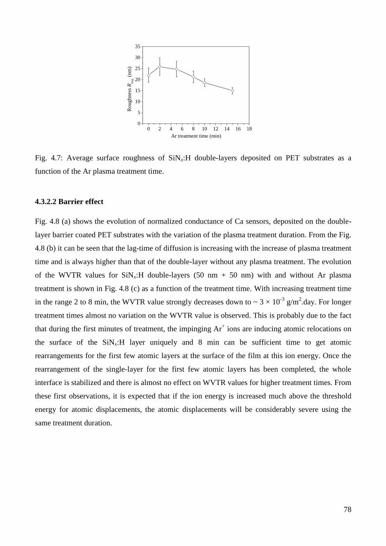
78
0 2 4 6 8 10 12 14 16 180
5
10
15
20
25
30
35
Ro
ug
hn
ess
Ra
vg. (
nm
)
Ar treatment time (min)
Fig. 4.7: Average surface roughness of SiNx:H double-layers deposited on PET substrates as a
function of the Ar plasma treatment time.
4.3.2.2 Barrier effect
Fig. 4.8 (a) shows the evolution of normalized conductance of Ca sensors, deposited on the double-
layer barrier coated PET substrates with the variation of the plasma treatment duration. From the Fig.
4.8 (b) it can be seen that the lag-time of diffusion is increasing with the increase of plasma treatment
time and is always higher than that of the double-layer without any plasma treatment. The evolution
of the WVTR values for SiNx:H double-layers (50 nm + 50 nm) with and without Ar plasma
treatment is shown in Fig. 4.8 (c) as a function of the treatment time. With increasing treatment time
in the range 2 to 8 min, the WVTR value strongly decreases down to ~ 3 × 10⁻³
g/m2.day. For longer
treatment times almost no variation on the WVTR value is observed. This is probably due to the fact
that during the first minutes of treatment, the impinging Ar+ ions are inducing atomic relocations on
the surface of the SiNx:H layer uniquely and 8 min can be sufficient time to get atomic
rearrangements for the first few atomic layers at the surface of the film at this ion energy. Once the
rearrangement of the single-layer for the first few atomic layers has been completed, the whole
interface is stabilized and there is almost no effect on WVTR values for higher treatment times. From
these first observations, it is expected that if the ion energy is increased much above the threshold
energy for atomic displacements, the atomic displacements will be considerably severe using the
same treatment duration.

79
0 25 50 75 100 125 150 175 2000.0
0.2
0.4
0.6
0.8
1.0N
orm
aliz
ed C
onduct
ance
(S
)
Time (hour)
2 min treatment
5 min treatment
8 min treatment
10 min treatment
15 min treatment
0 2 4 6 8 10 12 14 16 18 200
5
10
15
20
25
30
35
40
45
50
Lag
-tim
e (h
our)
Ar Treatment time (min)
(a) (b)
0 2 4 6 8 10 12 14 16 18 2010
-3
10-2
WV
TR
(g
/m2.d
ay)
Ar treatment time (min)
(c)
Fig. 4.8: (a) Normalised conductance of Ca sensors deposited on barrier coated PET substrates
versus time for two 50 nm thick SiNx:H single-layers separated by Ar plasma surface treatment for
different plasma exposure times. (b) Evolution of the “lag-time” versus the Ar plasma treatment time
of the SiNx:H films as a function of the Ar plasma exposure time. (c) Evolution of WVTR values
versus the Ar plasma treatment time of the SiNx:H films as a function of the Ar plasma exposure
time.
4.3.3 Effect of argon treatment on multilayers for 8 min duration
The best treatment time (8 min) obtained from the above discussions has been kept fixed to develop
barrier layers with increasing number of stacked layers. The other parameters, such as power density
and working pressure, remain fixed at 350 mW/cm2 and 50 mTorr respectively. The number of layers
(m) is varied from 2 to 5, in order to increase the total barrier thickness.
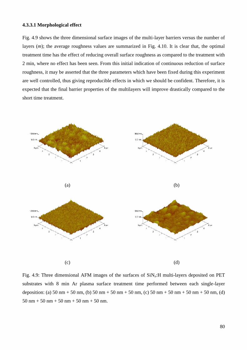
80
4.3.3.1 Morphological effect
Fig. 4.9 shows the three dimensional surface images of the multi-layer barriers versus the number of
layers (m); the average roughness values are summarized in Fig. 4.10. It is clear that, the optimal
treatment time has the effect of reducing overall surface roughness as compared to the treatment with
2 min, where no effect has been seen. From this initial indication of continuous reduction of surface
roughness, it may be asserted that the three parameters which have been fixed during this experiment
are well controlled, thus giving reproducible effects in which we should be confident. Therefore, it is
expected that the final barrier properties of the multilayers will improve drastically compared to the
short time treatment.
(a) (b)
(c) (d)
Fig. 4.9: Three dimensional AFM images of the surfaces of SiNx:H multi-layers deposited on PET
substrates with 8 min Ar plasma surface treatment time performed between each single-layer
deposition: (a) 50 nm + 50 nm, (b) 50 nm + 50 nm + 50 nm, (c) 50 nm + 50 nm + 50 nm + 50 nm, (d)
50 nm + 50 nm + 50 nm + 50 nm + 50 nm.

81
50 100 150 200 250 3000
5
10
15
20
25
Ro
ug
hn
ess,
Rav.
(nm
)
Multilayer thickness (nm)
Fig. 4.10: Average surface roughness of SiNx:H multi-layers deposited on PET substrates with 8 min
Ar plasma surface treatment time performed between each single-layer deposition.
4.3.3.2 Optical effect
Figure 4.11 shows the optical data consisting of reflectance and the transmittance measurements of
the multi-layer structure (stack of 5 SiNx:H single-layers, each separated by 8 min of Ar+ plasma
treatment) deposited on PET substrates. The transmittance curve indicates that the multi-layer
structure is highly transparent (~ 80%) in the visible region. It can also be seen from Fig. 4.11 that
reflectance and transmittance of this multi-layer structure add to almost 100%, meaning that no
absorption takes place in the layers and the barrier structure can be perfectly used as a window layer
for organic electronic devices. Slight absorption below 450 nm wavelength is due to the plastic
substrate itself.
400 500 600 700 800 9000
20
40
60
80
100
Ref
lect
ance
/ T
ransm
itta
nce
(%
)
Wavelength (nm)
Reflectance (%)
Transmittance (%)
Fig. 4.11: Reflection and transmission spectra of SiNx:H multilayer (stack of 5 SiNx:H single-layers
each separated by 8 min Ar-treatment) deposited on PET substrate.
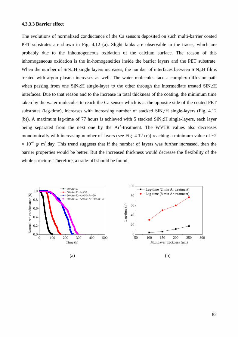
82
4.3.3.3 Barrier effect
The evolutions of normalized conductance of the Ca sensors deposited on such multi-barrier coated
PET substrates are shown in Fig. 4.12 (a). Slight kinks are observable in the traces, which are
probably due to the inhomogeneous oxidation of the calcium surface. The reason of this
inhomogeneous oxidation is the in-homogeneities inside the barrier layers and the PET substrate.
When the number of SiNx:H single layers increases, the number of interfaces between SiNx:H films
treated with argon plasma increases as well. The water molecules face a complex diffusion path
when passing from one SiNx:H single-layer to the other through the intermediate treated SiNx:H
interfaces. Due to that reason and to the increase in total thickness of the coating, the minimum time
taken by the water molecules to reach the Ca sensor which is at the opposite side of the coated PET
substrates (lag-time), increases with increasing number of stacked SiNx:H single-layers (Fig. 4.12
(b)). A maximum lag-time of 77 hours is achieved with 5 stacked SiNx:H single-layers, each layer
being separated from the next one by the Ar+-treatment. The WVTR values also decreases
monotonically with increasing number of layers (see Fig. 4.12 (c)) reaching a minimum value of ~2
× 10-4
g/ m2.day. This trend suggests that if the number of layers was further increased, then the
barrier properties would be better. But the increased thickness would decrease the flexibility of the
whole structure. Therefore, a trade-off should be found.
0 100 200 300 400 5000.0
0.2
0.4
0.6
0.8
1.0
No
rmal
ized
co
nd
uct
ance
(S
)
Time (h)
50+Ar+50
50+Ar+50+Ar+50
50+Ar+50+Ar+50+Ar+50
50+Ar+50+Ar+50+Ar+50+Ar+50
50 100 150 200 250 3000
20
40
60
80
100
Lag
-tim
e (h
)
Multilayer thickness (nm)
Lag-time (2 min Ar treatment)
Lag-time (8 min Ar treatment)
(a) (b)

83
50 100 150 200 250 30010
-4
10-3
10-2
WVTR (2 min Ar treatment)
WVTR (8 min Ar treatment) W
VT
R (
g/m
2.d
ay)
Multilayer thickness (nm)
(c)
Fig. 4.12: (a) Normalised conductance of Ca sensors deposited on barrier coated PET substrates
versus time for SiNx:H multi-layers separated by 8 min Ar plasma surface treatment. (b) Evolution of
the lag-time versus the SiNx:H multi-layer thickness. (c) Evolution of WVTR values versus the
SiNx:H multi-layer thickness. The evolutions of lag-time and WVTR for the SiNx:H multi-layers
with 2 min Ar plasma treatment are shown for comparison.
4.4 IMPACT OF THE POWER DENSITY OF ARGON TREATMENT
The above measurements have been carried out using a fixed power density of 350 mW/cm2. Power
density has an important role to determine the kinetic energy of the impinging ions as well as the ion
energy fluence [172]. In order to investigate the impact of power density on the overall barrier
properties, the power density has been varied from a lower value of 85 mW/cm2 to a higher value of
700 mW/cm2. The treatment time is kept constant at the best treatment duration of 8 min and the
working pressure remains same as above (50 mTorr). The investigations are performed using a
double-layer structure (total thickness = 100 nm) in order to simplify both the deposition process for
all the concerned samples and the subsequent interpretations.

84
Power
density,
Pw
(mW/cm2)
Pressure,
pg
(mTorr)
VBias
(V)
Maximum
ion
energy
(eV)
Time, t
(s)
Ion flux, Fi
(cm-2
.s-1
)
Ion fluence
(cm-2
)
Ion energy
fluence
(eV.cm-2
)
85 50 -10 10 480 5.4 × 10¹⁶
26 × 1018
26 × 1019
350 50 -20 20 480 1.1 × 10¹⁷
53 × 1018
11 × 1020
400 50 -28 28 480 8 × 10¹⁶
38 × 1018
12 × 1020
450 50 -38 38 480 7.6 × 10¹⁶
36 × 1018
14 × 1020
700 50 -100 100 480 4.4 × 10¹⁶
21 × 1018
21 × 1020
Table 4.2: Variations of maximum ion energy with the change of RF power density.
4.4.1 Morphological effect
Fig. 4.13 shows the variation of average surface roughness values for stack of two 50 nm thick
SiNx:H single-layers separated by Ar plasma surface treatment for different RF power densities.
When the power density is low (85 mW/cm2) which corresponds to the maximum Ar ion
bombardment energy of 10 eV, there is no significant variation of roughness as compared to the
double layer structure without any plasma treatment. This is due to the fact that the energy is quite
low to rearrange the surface atoms and needs higher treatment time in order to attain sufficient ion
energy fluence and smoothing effect. The change of surface roughness after this power density is
significantly dominated by the energy of the impinging ions since the ion energy fluence is more or
less similar for those power density values. With increasing power density values, the energy of ions
increases as well and the effect on surfaces becomes more pronounced. The lowest average
roughness (18 nm) is achieved for 400 mW/cm2, which corresponds to the maximum ion energy of
28 eV. It should be noted here that this energy (28 eV) is just above the maximum surface atomic
displacement threshold (25 eV for Si) and below the bulk atomic displacement threshold (40 eV for
Si) and therefore, it is expected that at this energy there is sufficient surface atom rearrangement for
few atomic layers which results in surface roughness reduction. The roughness values increases after
that and reaches a maximum value of 22.8 nm for 700 mW/cm2 which corresponds to the maximum
energy of 100 eV, an energy higher enough for Si atomic sputtering threshold (50 eV) and induces
damage of the surface.

85
0 200 400 600 800 100010
15
20
25
30
Ro
ug
hn
ess,
Rav. (
nm
)
Power density (mW/cm2)
Fig. 4.13: Variation average surface roughness for two 50 nm thick SiNx:H single-layers separated by
Ar plasma surface treatment for different RF power densities.
4.4.2 Barrier effect
The evolutions of the normalized conductance of the calcium sensors are shown in Fig. 4.14 (a) and
(b). The variations of lag-time and WVTR with increase of power-density are shown in Fig. 4.14 (c)
and (d) respectively. Three separate regions are observed for the barrier properties and vary in a
similar way of the variation of average surface roughness values (Fig. 4.13). In the first region, the
power density is increased up to 85 mW/cm2, which corresponds to maximum ion energy of ~10 eV
impinging on the sample surface (see Table 4.2). Within the uncertainty of conductance decrease
with time, no effect on the barrier properties can be observed. This is probably due to the fact that,
the maximum ion energy is below the minimum surface atom displacement threshold for Si (~15
eV). When the power density is increased (350 mW/cm2), the maximum ion energy also increases
(see Table 4.2). For a fixed working pressure, when the maximum energy is around ~20 eV, there is
a drastic change in the barrier properties. The lag-time is increased up to 30 h and the WVTR is
decreased down to 3 × 10⁻³
g/m2.day. This is probably due to the fact that, the ion kinetic energy
approaches the maximum surface atom displacement threshold energy for Si (~25 eV). If the power
density is increased again up to 400 mW/cm2, then the maximum ion kinetic energy (28 eV) is above
the maximum surface atom displacement threshold energy. The barrier properties are further
improved. The lag-time is increased up to 35 h and the WVTR is decreased down to 9.2 × 10⁻⁴
g/m2.day. An interesting feature occurs when the power density is increased again up to 450
mW/cm2. Clearly the normalized conductance curve shows a net degradation compared to the
conductance curve obtained for 400 mW/cm2. The lag-time reduces and the WVTR increases. This is
probably because of the fact that, the maximum ion energy (38 eV) is close to the maximum bulk
displacement threshold energy for Si (~40 eV) and possibly some damage or sputtering of the film

86
begins to occur with very low sputtering yield. Thus, it can be concluded that with the increase of
maximum ion kinetic energy to such a value (38 eV), the surface atoms and few atomic layers of the
bulk have been rearranged and some other surface atoms have been sputtered away, damaging
somewhat the uniquely treated interface. In other words, it seems that the optimum ion energy giving
the minimum WVTR value has been overcome. Finally, when the power density is increased
drastically up to 700 mW/cm2, the maximum ion energy corresponds to ~100 eV. The barrier
properties degrade considerably at this ionic treatment. The lag-time decreases sharply (3 h) and the
WVTR increases above the value obtained for double-layer without any Ar treatment or with 85
mW/cm2 treatment. This effect confirms that Ar ions with an energy of 100 eV (and perhaps below)
degrade totally the uniquely treated interface between the two SiNx:H single-layers.
0 20 40 60 80 100 120 140 160 1800.0
0.2
0.4
0.6
0.8
1.0
Norm
aliz
ed c
onduct
ance
(S
)
Time (h)
No treatment
85 mW/cm2
350 mW/cm2
400 mW/cm2
450 mW/cm2
700 mW/cm2
0 2 4 6 8 10 12 14 16 18 200.0
0.2
0.4
0.6
0.8
1.0
Norm
aliz
ed c
onduct
ance
(S
)
Time (h)
No treatment
85 mW/cm2
700 mW/cm2
(a) (b)
0 200 400 600 800 10000
10
20
30
40
50
Lag
-tim
e (h
)
Power density (mW/cm2)
0 200 400 600 800 1000
10-3
10-2
WV
TR
(g
/m2.d
ay)
Power density (mW/cm2)
(c) (d)
Fig. 4.14: (a) Normalized conductance of Ca sensors deposited on barrier coated PET substrates
versus time for two 50 nm thick SiNx:H single-layers separated by Ar plasma surface treatment for
different RF power densities. (b) Zoom of the first region of conductances. (c) Evolution of the “lag-
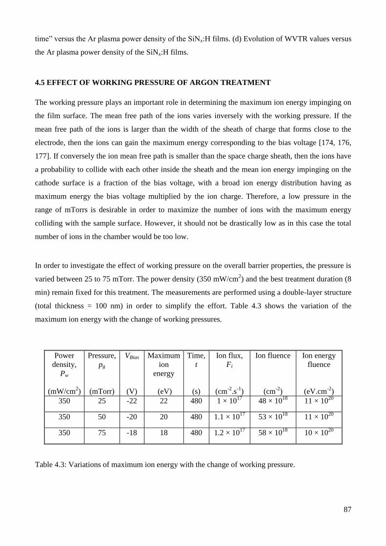
87
time” versus the Ar plasma power density of the SiNx:H films. (d) Evolution of WVTR values versus
the Ar plasma power density of the SiNx:H films.
4.5 EFFECT OF WORKING PRESSURE OF ARGON TREATMENT
The working pressure plays an important role in determining the maximum ion energy impinging on
the film surface. The mean free path of the ions varies inversely with the working pressure. If the
mean free path of the ions is larger than the width of the sheath of charge that forms close to the
electrode, then the ions can gain the maximum energy corresponding to the bias voltage [174, 176,
177]. If conversely the ion mean free path is smaller than the space charge sheath, then the ions have
a probability to collide with each other inside the sheath and the mean ion energy impinging on the
cathode surface is a fraction of the bias voltage, with a broad ion energy distribution having as
maximum energy the bias voltage multiplied by the ion charge. Therefore, a low pressure in the
range of mTorrs is desirable in order to maximize the number of ions with the maximum energy
colliding with the sample surface. However, it should not be drastically low as in this case the total
number of ions in the chamber would be too low.
In order to investigate the effect of working pressure on the overall barrier properties, the pressure is
varied between 25 to 75 mTorr. The power density (350 mW/cm2) and the best treatment duration (8
min) remain fixed for this treatment. The measurements are performed using a double-layer structure
(total thickness = 100 nm) in order to simplify the effort. Table 4.3 shows the variation of the
maximum ion energy with the change of working pressures.
Power
density,
Pw
(mW/cm2)
Pressure,
pg
(mTorr)
VBias
(V)
Maximum
ion
energy
(eV)
Time,
t
(s)
Ion flux,
Fi
(cm-2
.s-1
)
Ion fluence
(cm-2
)
Ion energy
fluence
(eV.cm-2
)
350 25 -22 22 480 1 × 10¹⁷
48 × 1018
11 × 1020
350 50 -20 20 480 1.1 × 10¹⁷
53 × 1018
11 × 1020
350 75 -18 18 480 1.2 × 10¹⁷
58 × 1018
10 × 1020
Table 4.3: Variations of maximum ion energy with the change of working pressure.
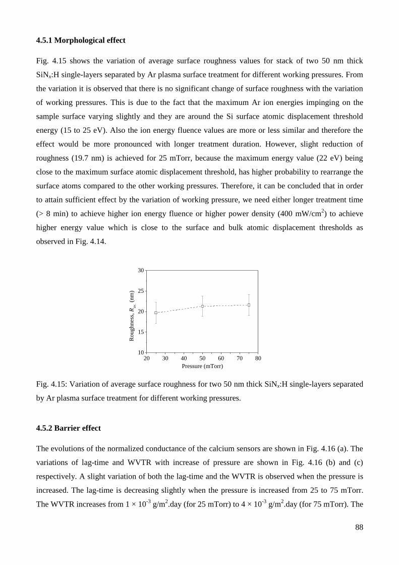
88
4.5.1 Morphological effect
Fig. 4.15 shows the variation of average surface roughness values for stack of two 50 nm thick
SiNx:H single-layers separated by Ar plasma surface treatment for different working pressures. From
the variation it is observed that there is no significant change of surface roughness with the variation
of working pressures. This is due to the fact that the maximum Ar ion energies impinging on the
sample surface varying slightly and they are around the Si surface atomic displacement threshold
energy (15 to 25 eV). Also the ion energy fluence values are more or less similar and therefore the
effect would be more pronounced with longer treatment duration. However, slight reduction of
roughness (19.7 nm) is achieved for 25 mTorr, because the maximum energy value (22 eV) being
close to the maximum surface atomic displacement threshold, has higher probability to rearrange the
surface atoms compared to the other working pressures. Therefore, it can be concluded that in order
to attain sufficient effect by the variation of working pressure, we need either longer treatment time
(> 8 min) to achieve higher ion energy fluence or higher power density (400 mW/cm2) to achieve
higher energy value which is close to the surface and bulk atomic displacement thresholds as
observed in Fig. 4.14.
20 30 40 50 60 70 8010
15
20
25
30
Roughnes
s, R
av. (
nm
)
Pressure (mTorr)
Fig. 4.15: Variation of average surface roughness for two 50 nm thick SiNx:H single-layers separated
by Ar plasma surface treatment for different working pressures.
4.5.2 Barrier effect
The evolutions of the normalized conductance of the calcium sensors are shown in Fig. 4.16 (a). The
variations of lag-time and WVTR with increase of pressure are shown in Fig. 4.16 (b) and (c)
respectively. A slight variation of both the lag-time and the WVTR is observed when the pressure is
increased. The lag-time is decreasing slightly when the pressure is increased from 25 to 75 mTorr.
The WVTR increases from 1 × 10⁻³
g/m2.day (for 25 mTorr) to 4 × 10
-3 g/m
2.day (for 75 mTorr). The

89
maximum ion energy varies between 18 to 22 eV, which is around the energy threshold for the Si
surface atom displacement. The improvement of barrier properties at comparatively lower working
pressure (25 mTorr) is probably due to the fact that when the pressure is lower than 50 mTorr, the
ions have fewer collisions, but the number of ions impinging on the films surface can gain a higher
maximum energy (22 eV). Thus, the effect on the surface is more pronounced and the barrier
properties improve.
On the contrary, when pressure is higher than 50 mTorr, the maximum energy gained by the Ar ions
is lower (18 eV). Therefore, the effect on the SiNx:H surface is less pronounced as Si atomic
displacement is more difficult to reach in these conditions. The barrier properties are slightly
degraded compared with the 50 mTorr treatment.
0 20 40 60 80 100 120 1400.0
0.2
0.4
0.6
0.8
1.0
No
rmal
ized
Co
nd
uct
ance
(S
)
Time (h)
25 mTorr
50 mTorr
75 mTorr
20 30 40 50 60 70 8020
25
30
35
Lag
-tim
e (h
)
Pressure (mTorr)
(a) (b)
20 30 40 50 60 70 8010
-4
10-3
10-2
WV
TR
(g
/m2.d
ay)
Pressure (mTorr)
(c)
Fig. 4.16: (a) Normalized conductance of Ca sensors deposited on barrier coated PET substrates
versus time for two 50 nm thick SiNx:H single-layers separated by Ar plasma surface treatment for
different working pressures. (b) Evolution of the “lag-time” versus the working pressure. (c)

90
Evolution of WVTR values versus the working pressure.
4.6 EFFECT OF BEST TREATMENT PARAMETERS ON THE MULTILAYERS
The above mentioned optimizations for the Ar treatment on SiNx:H single-layers are considered to
develop multilayers of SiNx:H films in order to investigate their combined effect on the overall
barrier properties. However, it should be noted that the above optimizations have been carried out
independently and the combined effect of power density and pressure is controlling the bias voltage
and thus the maximum ion energy. Therefore, when all the above mentioned optimized parameters
are merged, we can consider that we are capable to control maximum ion energy compared to the Si
atomic displacement threshold. So we are able to improve the barrier properties, even though we are
convinced that the complete optimization of the four Ar treatment parameters should need further
studies. The optimized parameters used in this study are: 400 mW/cm2 power density, 25 mTorr
working pressure and 8 min of treatment duration. We measured that these parameters give rise to an
effective bias voltage of -30 V and thus the maximum ion energy impinging on the film surface is
~30 eV. The multilayers composed of 2 to 5 SiNx:H single-layer films are analyzed in order to see
the effect on morphological, optical and barrier properties.
4.6.1 Morphological effect
The surface topography of the multilayer SiNx:H films treated with the above mentioned optimized
parameters has been characterized using tapping mode AFM technique. Fig. 4.17 shows the surface
topography and Fig. 4.18 shows the average surface roughness variation with increase of the number
of layers. It is clear from the analysis that with the optimized Ar treatment parameters, the roughness
decreases quite drastically. Compared to previous roughness results for double-layer structures we
can notice that the roughness value (16 nm) obtained for 400 mW/cm2, 25 mTorr and 8 min is
smaller than that obtained (21.3 nm) for 350 mW/cm2, 50 mTorr and 8 min (see Fig. 4.7). This
example confirms the positive effect due to the optimization of power density and pressure together
and confirms as well that evolution of roughness versus multilayer thickness is a good indication of
the possible evolution of barrier properties versus multilayer thickness.
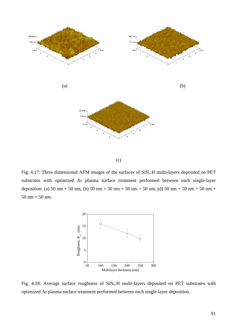
91
(a) (b)
(c)
Fig. 4.17: Three dimensional AFM images of the surfaces of SiNx:H multi-layers deposited on PET
substrates with optimized Ar plasma surface treatment performed between each single-layer
deposition: (a) 50 nm + 50 nm, (b) 50 nm + 50 nm + 50 nm + 50 nm, (d) 50 nm + 50 nm + 50 nm +
50 nm + 50 nm.
50 100 150 200 250 3000
5
10
15
20
Roughnes
s, R
av.
(nm
)
Multilayer thickness (nm)
Fig. 4.18: Average surface roughness of SiNx:H multi-layers deposited on PET substrates with
optimized Ar plasma surface treatment performed between each single-layer deposition.

92
4.6.2 Optical effect
Figure 4.19 shows the optical data consisting of reflectance and the transmittance measurements of
the multi-layer structure (stack of 5 SiNx single-layers, each separated by Ar+ plasma treatment)
deposited on PET substrates. The transmittance curve indicates that the multi-layer structure is
highly transparent (~ 80%) in the visible region. It can also be seen from Fig. 4.19 that reflectance
and transmittance of this multi-layer structure add to almost 100% in the visible range.
300 400 500 600 700 8000
20
40
60
80
100
Tra
nsm
itta
nce
/ R
efle
ctan
ce (
%)
Wavelength (nm)
Transmittance
Reflectance
Fig. 4.19: Reflection and transmission spectra of SiNx:H multilayer (stack of 5 SiNx:H single-layers
each separated by optimized Ar-treatment deposited on PET substrate).
4.6.3 Barrier effect
The normalized conductances of the Ca sensors deposited on such multi-layer barrier coated PET
substrates are shown in Fig. 4.20 (a). Kinks are also observed in the traces for higher thickness
barriers. These are due to slight in-homogeneities inside the barriers and PET substrates as discussed
before. The lag-time and WVTR values are evaluated from the evolutions and are shown in Fig. 4.20
(b) and (c) respectively. When the number (m) of single-layers treated with the optimized Ar
treatment conditions is increased from 2 to 5, the permeation path becomes considerably tortuous due
to the treated interfaces and increase of total film thickness. Thus the minimum time taken by the
water molecules to reach the Ca sensor surface increases and leads to an increased lag-time of
permeation up to 125 h for 5 stacked SiNx:H single-layers. Due to the same reason, the permeation
rate (WVTR) decreases monotonically when the number of SiNx:H single-layer increases. A
minimum WVTR of 7 × 10⁻⁵
g/m2.day is obtained for 5 stacked SiNx:H single-layers. This result
confirms the drastic effect of power density and pressure on the permeation barriers and roughness
values.

93
0 200 400 600 800 1000 12000.0
0.2
0.4
0.6
0.8
1.0N
orm
aliz
ed c
on
du
ctan
ce (
S)
Time (h)
50+Ar+50
50+Ar+50+Ar+50+Ar+50
50+Ar+50+Ar+50+Ar+50+Ar+50
50 100 150 200 250 3000
25
50
75
100
125
150
Lag
-tim
e (h
)
Multilayer coating thickness (nm)
(a) (b)
50 100 150 200 250 30010
-5
10-4
10-3
WV
TR
(g
/m2.d
ay)
Multilayer coating thickness (nm)
(c)
Fig. 4.20: (a) Evolution of normalized conductance of Ca sensor deposited on PET coated with
multi-layers of SiNx:H films treated by argon plasma. (b) Variation of “lag-time” with SiNx:H multi-
layer coating thickness (Ar treated). (c) Variation of WVTR values with SiNx:H multi-layer coating
thickness (Ar treated).
4.7 MECHANICAL PROPERTIES
Mechanical flexibility is an important property for the barrier layers for the utilization in flexible
organic optoelectronic devices. In addition to their requisite barrier properties, the encapsulation
layers should maintain their barrier performances during and after mechanical deformations. The
inorganic materials used as a permeation barrier are brittle in nature and due to the mechanical
deformation strain; stress is induced inside the films which develop cracks inside the inorganic films.
Cracking of the inorganic films make the whole barrier ineffective. According to Yanaka et al. [190],
onset strain for crack formation for thin oxide films is 1.3%, while Leterrier et al. [191] measured a

94
range of strains from 1.2% to 2.0% before the fracture. Suo et al. [192] have given a useful analysis
of the thin film mechanics. Whenever, a brittle inorganic film is deposited on a flexible under layer
(substrate) and the whole structure is bent with decreasing radius of curvature (r), the neutral axis,
where no compressive or tensile strain exists, shifts towards the film, reducing stress inside the film.
The strain inside the top film is given by
= ( 𝑠
2𝑟)
( 2 2)
( )( ) (4.7)
Where η = (df / ds) and χ = (Yf / Ys). df, ds, Yf and Ys belong to the film thickness, substrate thickness,
Young’s modulus of film and Young’s modulus of substrate respectively. Using moduli values of
5.53 [193] and 297 GPa for the PET substrate and the SiNx:H film, respectively, and 175 µm and 100
nm (two 50 nm double layer) for the substrate and film thickness, respectively, the variation of strain
with the radius of curvature is shown in Fig. 4.21. It is clear that the onset strain for crack formation
(~ 1.3%) is around 5 to 7 mm of radius of curvature.
The mechanical flexibility of the barrier structure has been investigated by bending permeation
barriers correspond to a double-layer (100 nm) [deposited using HW-CVD method and Ar treatment
in the conditions: Pw = 350 mW/cm2, pg = 50 mTorr and t = 8 min (see sub-section 4.3.3)] structure
with a radius of curvature of 5 mm for different cycles of bending. Ca degradation tests are
performed on such bent samples in order to assess the impact of bending on the permeation barrier
properties. It is obvious that at this curvature, some cracks are formed inside the films that should
damage the permeation barriers. However, this is an indirect result as the defect density inside the
films is not measured during this study.
Fig. 4.22 (a) shows the Ca degradation test results relative to different samples: one has not been
bent. So the black curve describes its normalized conductance evolution. The other two samples have
been bent for 100 (red curve) and 500 (blue curve) cycles respectively. The effect of bending on the
lag-time is shown in Fig. 4.22 (b) which shows a sharp decrease in lag-time during the first 100 times
of bending and whose magnitude of degradation continues after 100 cycles. The WVTR of the
samples also increases sharply during the first 100 times of bending and whose magnitude of
degradation continues after 100 cycles. The observations show that even-though the barrier
properties of the inorganic films can be drastically improved using argon plasma treatment, the
mechanical flexibility of the barriers is limited. After several cycles of bending, the barrier properties
become progressively worse.

95
Fig. 4.21: The strain induced in the double barrier layer with the variation of radius of curvature (r).
0 20 40 60 80 100 1200.0
0.2
0.4
0.6
0.8
1.0
No
rmal
ized
Co
nd
uct
ance
(S
)
Time (h)
No bending
100 times bending
500 times bending
0 100 200 300 400 5000
10
20
30
40L
ag-t
ime
(h)
Number of bending
(a) (b)
0 100 200 300 400 50010
-3
10-2
WV
TR
(g
/m2.d
ay)
Number of bending
(c)
Fig. 4.22: (a) Normalized conductance of Ca sensors deposited on barrier coated PET substrates
versus time for two 50 nm thick SiNx:H single-layers separated by Ar plasma surface treatment for
0 2 4 6 8 10 12 14 16 18 200
5
10
15
20
25
Radius of curvature (mm)
Top layer
str
ain
(%
)

96
different number of bendings (0, 100, 500). (b) Evolution of the “lag-time” versus the number of
bendings. (c) Evolution of WVTR values versus the number of bendings.
4.8 INTERPRETATION
The Ar plasma treatment with the above mentioned optimized parameters improves the permeation
barrier properties of SiNx:H films drastically. In order to interpret the above observations, it has been
necessary to analyze deeply the effect of plasma treatment on the SiNx:H films. Several
characterizations have been performed on two types of samples grown on c-Si wafers: as deposited
SiNx:H single-layer film (50 nm) and SiNx:H single-layer film (50 nm) with plasma treated on the
top surface. Two different plasma treatments have been carried out: plasma treated with optimized
treatment parameters (400 mW/cm2, 25 mTorr and 8 min) and plasma treated with 700 mW/cm
2, 50
mTorr and 8 min. For simplicity the samples are named as following (Table 4.4):
Sample Films on c-Si wafer Plasma treatment conditions
A SiNx:H single-layer film (50 nm) No treatment
B SiNx:H single-layer film (50 nm) 400 mW/cm2, 25 mTorr and 8 min (Emax = 30 eV)
C SiNx:H single-layer film (50 nm) 700 mW/cm2, 50 mTorr and 8 min (Emax = 100 eV)
Table 4.4: Samples used for different characterizations.
Those three kinds of samples have been analyzed to observe the plasma treatment effect on the
morphological, compositional and structural properties. The morphological analysis has been carried
out by tapping mode AFM, the compositional analysis have been performed by FTIR, XPS and
GDOES techniques and the morphological as well as structural characterization has been carried out
by XRR method.
4.8.1 Morphological analysis and interpretation
The AFM measurements are performed on as-grown and plasma-treated SiNx:H (50 nm) thin films
deposited on crystalline silicon wafers, shown in Fig. 4.23, in order to verify the modification of the
surface done by plasma treatment in different conditions. The as deposited SiNx:H films (sample A)
observed in Fig. 4.23 (a) exhibits a comparatively rough surface with 2.1 nanometer scale peaks on
the surface. It should be noted that 2.1 nm peak on c-Si wafer based SiNx:H is quite low value
compared to 23 nm peak observed on PET substrate based SiNx:H film (see Chapter 3). After

97
plasma treatment with the optimized treatment conditions (sample B) as shown in Fig. 4.23 (b)), the
film shows a flat surface: root mean squared (rms) roughness = 0.7 nm, corresponding to a reduction
of 67% compared to 2.1 nm. From this first result it is clear that ion treatment with 30 eV leads to a
surface modification which corresponds to a smoothing [194]. On the contrary, after plasma
treatment with 700 mW/cm2, 50 mTorr and 8 min (sample C), the film becomes more rough (rms
roughness = 2.7 nm).
The explanation for the decrease of surface roughness of SiNx:H film under the exposition to the
optimized plasma treatment with 400 mW/cm2, 25 mTorr and 8 min (sample B) is related to the
minimization of surface energy during the impact of the incident Ar ion flux on the first few atomic
layers of the film. When the plasma is sustained, Ar ions issued from the quasi-neutral region and
crossing the interface quasi-neutral region/cathode sheath can gain sufficient energy, depending on
the working pressure, to kick on the surface atoms of the film. The total energy brought every second
to this surface involves the ion flux directed towards the surface and the mean energy of these ions.
Moreover, the maximum energy in the ion energy distribution, issued from the electron energy
distribution function, is competing with the surface or bulk atomic displacement threshold in the
solid. When maximum ion energy reaches or exceeds the surface displacement threshold (15 to 25
eV for Si), there is a statistical rearrangement of the surface atoms minimizing the effective surface
area and thus the surface energy of the system under consideration. Minimization of the effective
surface area is equivalent to the decrease of the surface roughness [195].
For the 400 mW/cm2 power density used for the plasma treatment observed in Fig. 4.23 (b) the
maximum ion energy has been assessed as 30 eV (see subsection 4.6), an energy higher than the
energy needed for displacing Si atoms in the film surface (> 20 eV). This surface rearrangement
(displacement of Si atoms relative to N atoms) can be the efficient way for inhibiting the diffusion of
water molecules from one SiNx:H layer to the next one, thus improving drastically the permeation
barrier, what has been observed in Fig. 4.20 for five stacked SiNx:H layers treated with such Ar
plasma conditions.
For the 700 mW/cm2 power density used for the plasma treatment observed in Fig. 4.23 (c), the
maximum ion energy has been assessed as 100 eV (see Table 4.6). In that case this energy is much
higher than the surface and bulk atomic displacement thresholds (15 to 40 eV) and higher than the
sputtering threshold (~ 40 eV for Si). It is also slightly higher than the implantation energy of Ar in
the solids (> 60 eV). The ion flux with such an energy is producing damage to the SiNx:H surface.
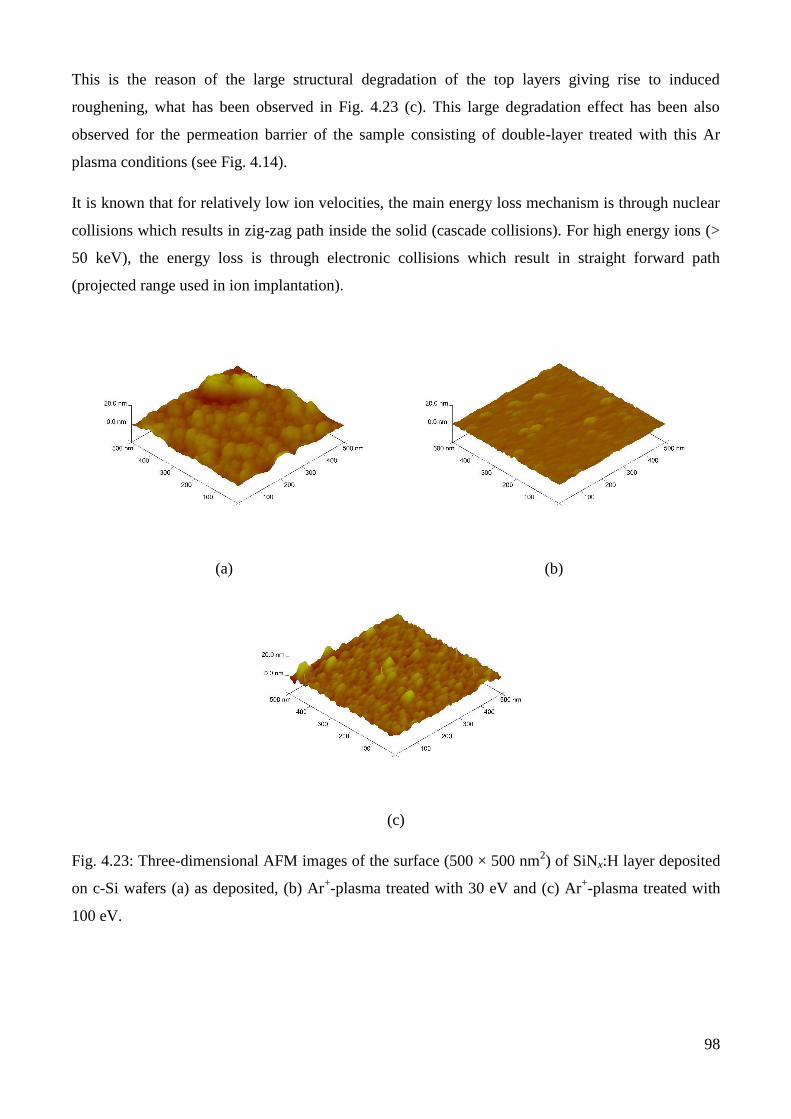
98
This is the reason of the large structural degradation of the top layers giving rise to induced
roughening, what has been observed in Fig. 4.23 (c). This large degradation effect has been also
observed for the permeation barrier of the sample consisting of double-layer treated with this Ar
plasma conditions (see Fig. 4.14).
It is known that for relatively low ion velocities, the main energy loss mechanism is through nuclear
collisions which results in zig-zag path inside the solid (cascade collisions). For high energy ions (>
50 keV), the energy loss is through electronic collisions which result in straight forward path
(projected range used in ion implantation).
(a) (b)
(c)
Fig. 4.23: Three-dimensional AFM images of the surface (500 × 500 nm2) of SiNx:H layer deposited
on c-Si wafers (a) as deposited, (b) Ar+-plasma treated with 30 eV and (c) Ar
+-plasma treated with
100 eV.

99
4.8.2 Compositional analysis and interpretation
4.8.2.1 FTIR analysis
FTIR absorption analysis has been carried out with the three above mentioned samples. The relative
absorption intensities corresponding to the different band structures are shown in Fig. 4.24 (a) and
(b). Four different bands are visible for the samples [84]: Si-N stretching mode (860 cm-1
), Si-H (630
cm-1
) bending mode and Si-H2 stretching mode (2100 cm-1
), as well as N-H stretching mode (3340
cm-1
). Si-O stretching mode (1060 cm-1
) and N-H bending mode (1160 cm-1
) vibrations are not
visible in the spectrum, probably due to the large amount of moisture inside the FTIR setup and
insufficient N2 purging. All the vibration peaks shows no difference for as-grown and Ar+ treated
samples, except the absorption region around 2100 cm-1
which is zoomed in Fig. 4.24 (a). The
integrated absorption peaks corresponding to different bonds are summarized in Fig. 4.24 (c).
Concentrations of chemical species can be calculated as [196]
𝑁𝑐 𝑖𝑐 𝑐𝑖 ( ) =
(𝑐 ) 𝑒 (𝑐 2)
(4.8)
Where A is the height of integrated absorbance peak (dimensionless parameter), d is the film
thickness and Seff is the effective absorption cross-section. The values of Seff for Si-N bonds is 1.6 ×
10-19
cm2 [197], for Si-H bonds is 0.57 × 10
-19 cm
2 [198] and for N-H bonds is 0.8 × 10
-19 cm
2 [199]
respectively. Table 4.5 shows the concentrations of chemical species obtained from the above
equation. It can be noted that the total concentration of Si-N bonds (~11.15 × 10²²
cm-3
) is close to
the stoichiometric Si3N4, which is about 15.5 × 10²²
cm-3
[200]. There is no significant change in
chemical compositions corresponding to Si-N and N-H bonds for as-deposited and plasma treated
samples, except slight modifications of Si-H2 bonds.
The Si-H2 chemical concentration is reduced when the SiNx:H film is treated with Ar+-plasma treated
with optimized parameters (sample B). It was reported that SiH2 bonds originating the absorption at
≈2100 cm-1
are grouped and situated on the surfaces of micro and nano-sized voids in amorphous
phase. The minimization of the Si-H2 chemical concentration with the optimized Ar+ treatment
conditions is possibly due to the reduction of micro-voids or nano-voids [201] in the SiNx:H film and
thus an indication of the SiNx:H film densification [202]. The reduction of micro-voids or nano-voids
could be related to the surface atom displacement by the energetic (~30 eV) Ar+ ions, which relocate
the surface atoms to another lattice sites or defect positions.
When the SiNx:H film is treated with highly energetic (~100 eV) Ar+ ions (sample C), noticeably the
Si-H2 chemical concentration at 2100 cm-1
increases as compared to the as deposited sample. This is
because of the enlargement of the number of micro-voids at the surface or possibly inside the bulk,

100
due to the high bombardment damage of the film by highly energetic ions. The observations are
coherent with the structural deterioration of the permeation barriers.
600 700 800 900 2070 2100 2130
Wavenumber (cm-1
)
Sample A
Si-H Si-N Si-H2
Ab
sorb
ance
(a.
u.)
Sample B
Sample C
3300 3350 3400
Ab
sorb
ance
(a.
u.)
Wavenumber (cm-1
)
Sample A
Sample B
Sample C
N-H
(a) (b)
500 1000 1500 2000 2500 3000 3500
Sample A
Sample B
Sample C
Inte
gra
ted
ab
sorp
tio
n (
a.u
.)
Wavenumber (cm-1
)
Si-H2 (2100 cm
-1)
Si-H (630 cm-1)
N-H (3340 cm-1
)
Si-N (860 cm-1)
(c)
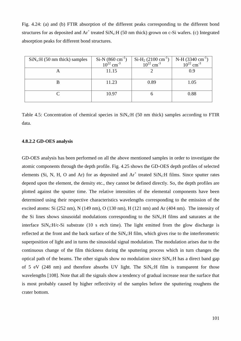
101
Fig. 4.24: (a) and (b) FTIR absorption of the different peaks corresponding to the different bond
structures for as deposited and Ar+ treated SiNx:H (50 nm thick) grown on c-Si wafers. (c) Integrated
absorption peaks for different bond structures.
SiNx:H (50 nm thick) samples Si-N (860 cm-1
)
1022
cm-3
Si-H2 (2100 cm-1
)
1022
cm-3
N-H (3340 cm-1
)
1022
cm-3
A 11.15 2 0.9
B
11.23 0.89 1.05
C 10.97 6 0.88
Table 4.5: Concentration of chemical species in SiNx:H (50 nm thick) samples according to FTIR
data.
4.8.2.2 GD-OES analysis
GD-OES analysis has been performed on all the above mentioned samples in order to investigate the
atomic components through the depth profile. Fig. 4.25 shows the GD-OES depth profiles of selected
elements (Si, N, H, O and Ar) for as deposited and Ar+ treated SiNx:H films. Since sputter rates
depend upon the element, the density etc., they cannot be defined directly. So, the depth profiles are
plotted against the sputter time. The relative intensities of the elemental components have been
determined using their respective characteristics wavelengths corresponding to the emission of the
excited atoms: Si (252 nm), N (149 nm), O (130 nm), H (121 nm) and Ar (404 nm). The intensity of
the Si lines shows sinusoidal modulations corresponding to the SiNx:H films and saturates at the
interface SiNx:H/c-Si substrate (10 s etch time). The light emitted from the glow discharge is
reflected at the front and the back surface of the SiNx:H film, which gives rise to the interferometric
superposition of light and in turns the sinusoidal signal modulation. The modulation arises due to the
continuous change of the film thickness during the sputtering process which in turn changes the
optical path of the beams. The other signals show no modulation since SiNx:H has a direct band gap
of 5 eV (248 nm) and therefore absorbs UV light. The SiNx:H film is transparent for those
wavelengths [108]. Note that all the signals show a tendency of gradual increase near the surface that
is most probably caused by higher reflectivity of the samples before the sputtering roughens the
crater bottom.

102
Although in a commercial c-Si wafer the O-concentration is quite low (1015
- 5× 10¹⁶
atoms/cm3)
[203], the O-signal shows some amount of oxygen inside the crystalline silicon wafer, which is
probably due to the intrinsic atmosphere inside the glow discharge chamber. The same argument is
valid for H content inside the c-Si wafer. However, if the concentrations of O and H are taken as a
baseline of measurement, the respective concentrations inside the as deposited SiNx:H film is very
low compared to Si and N concentrations, which in turns confirms the comparatively higher density
(2.83 g/cm3) of the HW-CVD grown SiNx:H film as discussed in Chapter 3. Slight bump of the O-
line at the film-substrate interface is due to the oxide layer formed on the c-Si wafer owing to the
imperfect cleaning procedure.
When the SiNx:H film is Ar+ plasma treated with the optimized treatment parameters (sample B), the
depth profile shows almost no significant modifications for the atomic components, except slight
reduction of the amount of H near the surface, which is probably due to reduction of nano-voids as
already observed by FTIR analysis. This observation is consistent with the fact that at such treatment
energy the bulk layer is not disturbed, while the modifications at the very top surface are not
completely visible here.
The compositional change in SiNx:H film is pronounced when the sample is treated by Ar+ plasma
with -100 V bias voltage (sample C). Due to this energetic ion bombardment causing atomic
sputtering, structural damage induces some porosity in the film. This porosity is confirmed by the
increase of H and O contents as shown in Fig. 4.25, probably due to the adsorption of moisture and
oxygen inside the nano or micro voids. Some Ar atoms (1 ppm < CAr < 0.1 at %) are also observed
implanted in first few layers of the film inside the film. Implantation of Ar atoms inside Si up to less
than 2 nm from the surface at 60 eV ionic bombardments has been reported by Al-Bayati et al [204]
and thus making our observation consistent.

103
0 5 10 15 20 250.0
0.2
0.4
0.6
0.8
1.0 H; N; O; Si
H'; N
'; O
'; Si
'
H''; N
''; O
''; Si
''; Ar
''
Norm
aliz
ed i
nte
nsi
ty (
V)
Etch time (s)
Si
N
O
HAr
Fig. 4.25: Depth profile of the atomic compositions for as deposited and Ar+ treated SiNx:H (50 nm
thick) grown on c-Si wafers. The single-prime compositions correspond to the sample B and double-
prime compositions correspond to the sample C.
4.8.2.3 XPS analysis
The above mentioned samples have been analyzed using X-ray photoelectron spectroscopy at
IRAMIS, CEA Saclay. The details of technical specifications are discussed in chapter 2. The XPS
spectrums of different chemical components corresponding to the above samples are shown in Fig.
4.26. The peaks corresponding to Si, N and O are fitted by Gaussian fitting method to obtain the
atomic concentrations of the elements. As observed from Fig. 4.26 (a) and (b), the as deposited
SiNx:H and Ar plasma treated (30 eV) shows no variations of the peak heights for Si and N
components. However, slight reduction (2 at %) of O is observed for 30 eV Ar treated sample (16 at
%) compared to sample A (18 at %), which is possibly due to reduction of micro-or nano voids
reducing the probability of adsorption of moisture from the atmosphere. Slight discrepancy of the N
atomic concentration is also observed compared to the GD-OES measurements.
The sample treated with 100 eV Ar ions, shows a higher concentration of O (30 at %). This is due to
increased porosity and increased roughness (see 4.8.1) inside the film due to the damage induced by
the higher energy ionic bombardments, which increases the possibility of adsorption of moisture
from the atmosphere. No Ar atom is detected for this sample which is in apparent contradiction to the
GD-OES measurements. As the detection limit of typical XPS measurement is 0.1 at %, thus it

104
confirms the low (< 0.1 at %) atomic percentage of Ar atom implantation inside the film observed by
GD-OES (see 4.8.2.2).
(a)

105
(b)
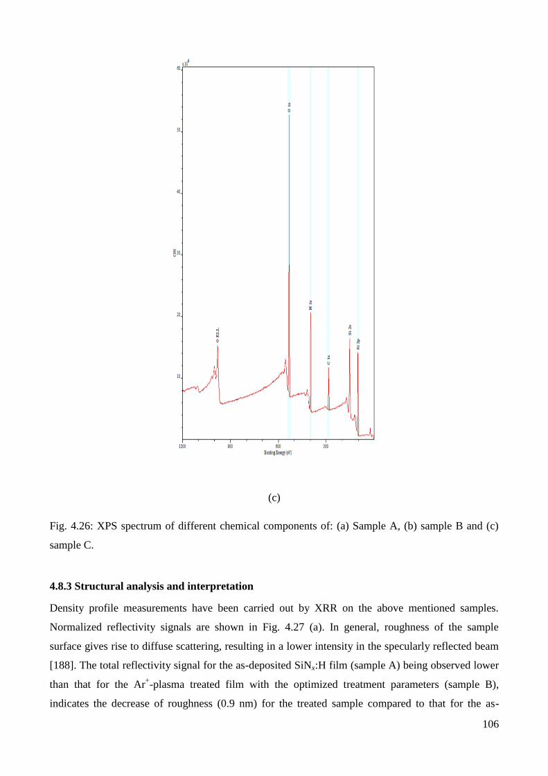
106
(c)
Fig. 4.26: XPS spectrum of different chemical components of: (a) Sample A, (b) sample B and (c)
sample C.
4.8.3 Structural analysis and interpretation
Density profile measurements have been carried out by XRR on the above mentioned samples.
Normalized reflectivity signals are shown in Fig. 4.27 (a). In general, roughness of the sample
surface gives rise to diffuse scattering, resulting in a lower intensity in the specularly reflected beam
[188]. The total reflectivity signal for the as-deposited SiNx:H film (sample A) being observed lower
than that for the Ar+-plasma treated film with the optimized treatment parameters (sample B),
indicates the decrease of roughness (0.9 nm) for the treated sample compared to that for the as-
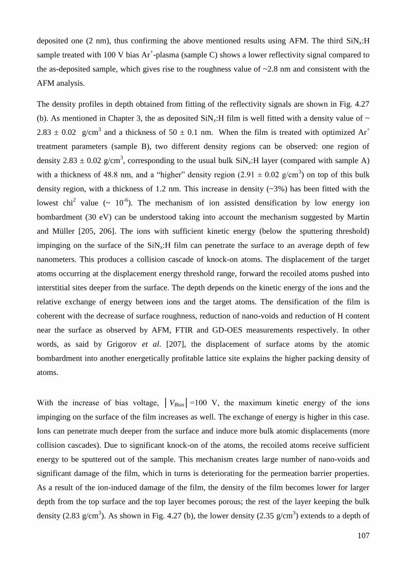
107
deposited one (2 nm), thus confirming the above mentioned results using AFM. The third SiNx:H
sample treated with 100 V bias Ar+-plasma (sample C) shows a lower reflectivity signal compared to
the as-deposited sample, which gives rise to the roughness value of ~2.8 nm and consistent with the
AFM analysis.
The density profiles in depth obtained from fitting of the reflectivity signals are shown in Fig. 4.27
(b). As mentioned in Chapter 3, the as deposited SiNx:H film is well fitted with a density value of ~
2.83 ± 0.02 g/cm3 and a thickness of 50 ± 0.1 nm.
When the film is treated with optimized Ar
+
treatment parameters (sample B), two different density regions can be observed: one region of
density 2.83 ± 0.02 g/cm3, corresponding to the usual bulk SiNx:H layer (compared with sample A)
with a thickness of 48.8 nm, and a “higher” density region (2.91 ± 0.02 g/cm3) on top of this bulk
density region, with a thickness of 1.2 nm. This increase in density (~3%) has been fitted with the
lowest chi2 value (~ 10
-6). The mechanism of ion assisted densification by low energy ion
bombardment (30 eV) can be understood taking into account the mechanism suggested by Martin
and Müller [205, 206]. The ions with sufficient kinetic energy (below the sputtering threshold)
impinging on the surface of the SiNx:H film can penetrate the surface to an average depth of few
nanometers. This produces a collision cascade of knock-on atoms. The displacement of the target
atoms occurring at the displacement energy threshold range, forward the recoiled atoms pushed into
interstitial sites deeper from the surface. The depth depends on the kinetic energy of the ions and the
relative exchange of energy between ions and the target atoms. The densification of the film is
coherent with the decrease of surface roughness, reduction of nano-voids and reduction of H content
near the surface as observed by AFM, FTIR and GD-OES measurements respectively. In other
words, as said by Grigorov et al. [207], the displacement of surface atoms by the atomic
bombardment into another energetically profitable lattice site explains the higher packing density of
atoms.
With the increase of bias voltage, VBias=100 V, the maximum kinetic energy of the ions
impinging on the surface of the film increases as well. The exchange of energy is higher in this case.
Ions can penetrate much deeper from the surface and induce more bulk atomic displacements (more
collision cascades). Due to significant knock-on of the atoms, the recoiled atoms receive sufficient
energy to be sputtered out of the sample. This mechanism creates large number of nano-voids and
significant damage of the film, which in turns is deteriorating for the permeation barrier properties.
As a result of the ion-induced damage of the film, the density of the film becomes lower for larger
depth from the top surface and the top layer becomes porous; the rest of the layer keeping the bulk
density (2.83 g/cm3). As shown in Fig. 4.27 (b), the lower density (2.35 g/cm
3) extends to a depth of

108
~7 nm from the surface. This observation is coherent with the GD-OES measurement, where the Ar
implantation depth is similar to the low density region.
0.04 0.06 0.08 0.10 0.12 0.14
q (Å-1)
No
rmal
ized
in
ten
sity
, I/
I 0
Sample A
Sample B
Sample C
0 10 20 30 40 50
1.86
2.17
2.48
2.79
2.28
2.47
2.66
2.85
2.28
2.47
2.66
2.85
Damaging
Distance from the substrate (nm)
Sample C
Densification
Den
sity
(g/c
m3) Sample B
Sample A
(a) (b)
Fig. 4.27: (a) XRR normalized reflection of the different SiNx:H samples (50 nm thick) grown on c-
Si wafers: sample A (red), sample B (black) and sample C (blue).(b) Density profile of the films.
4.8.4 General discussion on barrier improvement
We summarize here what has been observed and explained in the previous sub-headings of this
chapter. In Fig. 4.28 (a), the single-layers contain pin-holes through which water molecules can
easily diffuse. The argon plasma treatment with optimized treatment parameters (30 eV) induces a
denser top surface (1.2 nm thick) containing a lower number of micro-or-nano voids compared to the
bulk SiNx:H single-layer and hindering the native nucleation centers which were existing at the top
of the first SiNx:H layer (Fig. 4.28 (b)). This modified surface impedes the diffusion of water
molecules from the outside to enter into the pinholes. We grow a second SiNx:H layer on top of the
Ar treated surface with low probability of alignment of pinholes with the first layer (Fig. 4.28 (c)).
When these plasma treated SiNx:H layers are stacked together, the water molecules face a tortuous
diffusion path and the total time of diffusion throughout the whole barrier structures becomes longer.

109
Thus, the permeation barrier properties logically improve for this plasma treated barrier structures, as
observed in this chapter. Therefore, without creating a real physical interlayer as proposed by the
conventional barrier structures, this method provides a unique encapsulation procedure which is
viable in terms of throughput compared to the conventional barrier structures.
(a) (b) (c) (d)
Fig. 4.28: Schematic diagrams of steady state permeation of water molecules through different
structures of SiNx:H thin films deposited on PET substrates (not to scale): (a) single-layer of SiNx:H
(50 nm), (b) single-layer with Ar treated at the top surface (dark color), (c) second single-layer on top
of the Ar treated layer and (d) Ar treatment on top of the second single-layer.
4.9 SUMMARY OF CHAPTER 4
i. This chapter is comprised of a unique method of developing permeation barrier layers consisting
in multilayers of SiNx:H thin films and low energy plasma treatment between each successive
single-layer deposition.
ii. Several plasma treatment parameters (treatment duration, power density and working pressure)
are varied in order to achieve an optimal plasma treatment condition, which gives rise to drastic
reduction of the film surface roughness as well as a reduction of the WVTR values and increase
of the lag-time.
iii. The minimum WVTR obtained (7 × 10⁻⁵
g/m2.day) should be sufficient for the longer shelf-life-
time of organic electronic devices.
iv. The mechanical property of the barrier structure is investigated in order for this permeation
barrier to be utilized in real flexible organic electronic devices.
Substrate Substrate Substrate Substrate Substrate

110
v. Several characterizations are performed to interpret both the improvement and the deterioration
of barrier properties. Physical interpretations are given taking into account the different plasma
treatment parameters. For relatively high energy Ar ions, some Ar atoms have been detected
using glow discharge optical emission spectroscopy but not detected using X-ray photoelectron
spectroscopy, confirming the low concentration of Ar (< 0.1 at %) implanted below the surface.

111
CHAPTER 5
INORGANIC / ORGANIC HYBRID-LAYER FILMS
5.1 INTRODUCTION
The improvement in barrier performance of inorganic single layers such as SiNx:H films is limited
mainly by pinholes or nanometer-to-micron sized structural defects, which can favor the diffusion of
water molecules from the underlying SiNx:H film. As mentioned in chapter 4, a technique which
could make a break of the propagation of structural defects by decoupling the defects in consecutive
single-layers is needed. The conventional approach of developing encapsulation structures is based
on fabricating alternating inorganic and organic layers in order to minimize the propagation of
structural defects throughout the barriers. This common strategy involves sandwiching a smooth
organic layer between two inorganic layers [38, 69, 91-98] and thus creates a complex and tortuous
diffusion path for the water molecules throughout the whole structure.
Organic materials (e.g., polymers) are often robust but highly permeable to moisture, while single-
layers of inorganic materials (SiNx:H) are comparatively less permeable to moisture but extremely
fragile and contain structural defects. Thus, neither by itself is an effective permeation barrier for
flexible electronics. Such a conception has led to the design of multilayer barrier coatings consisting
of alternating thin films of inorganic and organic materials, with the hope to capitalize on both the
impermeability of the inorganic layers and the robustness of the organic layers [119].
The primary goal of this chapter is to develop high performance encapsulation barriers layers
applying alternating inorganic and organic layers on PET substrates. The particular interest of this
chapter is to investigate the effect of number of inorganic-organic interfaces on the overall barrier
performance. Two different deposition techniques (MDECR-PECVD and HW-CVD) for the growth
of the inorganic layers (SiNx:H) are utilized and the overall barrier properties are compared. The
permeation barrier quality depends largely on the deposition techniques. The organic layer of PMMA
[Poly (methyl methacrylate)] is deposited by the widely used spin–coating technique. Very recently,
several researchers have developed high quality organic films with very precise thickness and optical
properties. Initiated-CVD (i-CVD) is one of those techniques which could allow one to grow high
quality organic layers [69]. However, this particular technique is not extensively used and requires
years of research on this particular technique, which is out of the scope of this present thesis. Instead,
112
the particular attention is focussed on increasing the inorganic-organic interfaces to reduce the barrier
properties.
In the first section of this chapter, the specific growth conditions and characteristics of the MDECR-
PECVD grown SiNx:H films obtained from the previous dedicated works are summarized. The
barrier properties of the MDECR-PECVD grown SiNx:H single-layer films are investigated in order
to obtain the critical thickness parameter (dc) and compared with the HW-CVD grown single-layer
films which is described before in chapter 3. The structures of the hybrid layers are discussed after
that taking into account the requirements of the thickness of the individual layers. The growth
conditions of the organic layer are then introduced.
In the last section of this chapter, the impact of number of inorganic-organic interfaces for both
MDECR-PECVD and HW-CVD grown SiNx:H films are described in detail. Their optical properties
are also introduced in order to show the compatibility of the structures with the utilization in real
devices. Finally, the mechanical properties of the barrier structure are discussed taking into account
different number of cyclic bending.
5.2 MDECR-PECVD GROWN SILICON NITRIDE FILMS
5.2.1 Growth of thin films
The silicon nitride films (SiNx:H) are deposited in Matrix Distributed Electron Cyclotron Resonance
(MDECR) PECVD reactor which is a high plasma density low-pressure deposition technology used
for the fabrication of dielectric, functional and optical thin films for different applications. The
detailed description and schematic diagram of the reactor has been described previously in chapter 2.
The SiNx:H thin films are deposited on cleaned PET substrates with previously optimized deposition
conditions as listed below in table 5.1 [103-105].
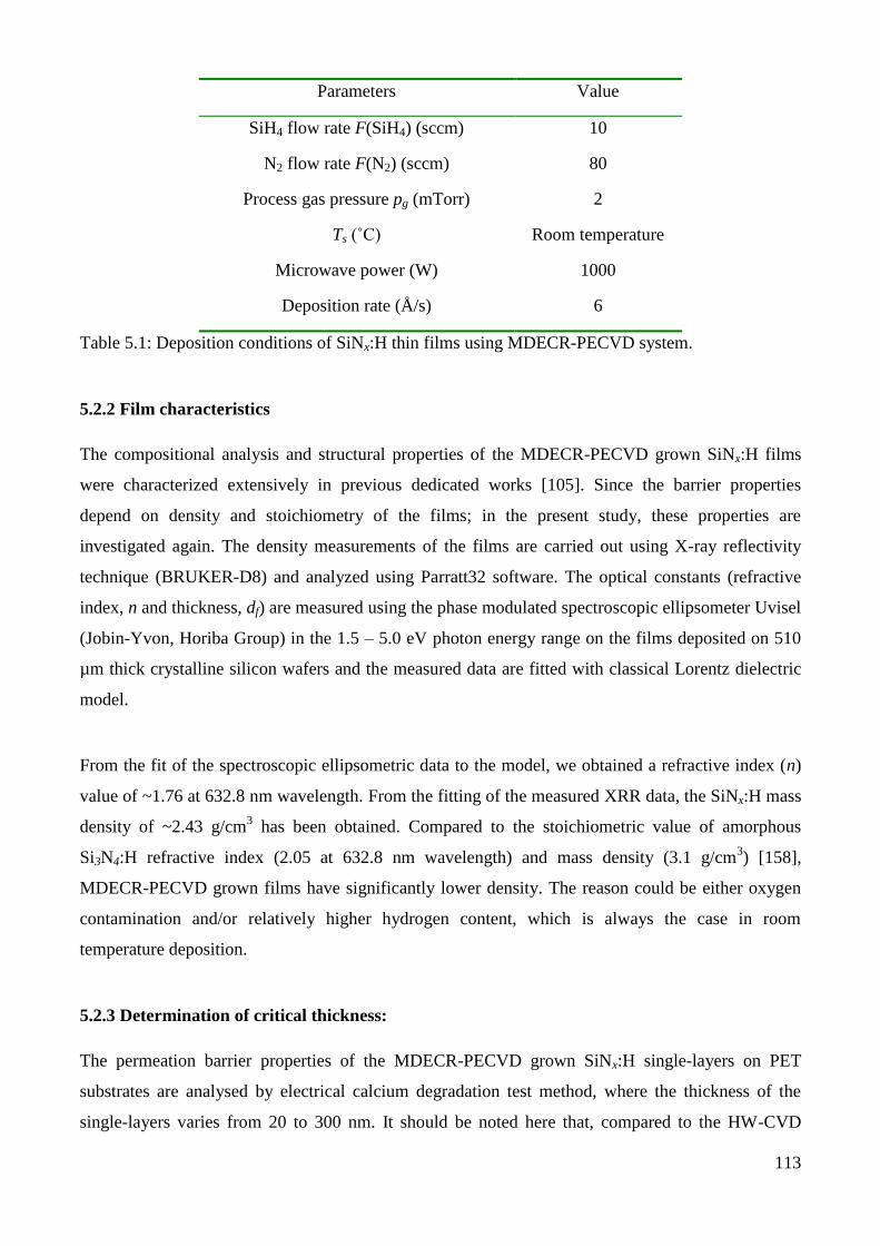
113
Parameters Value
SiH4 flow rate F(SiH4) (sccm) 10
N2 flow rate F(N2) (sccm) 80
Process gas pressure pg (mTorr) 2
Ts (˚C) Room temperature
Microwave power (W) 1000
Deposition rate (Å/s) 6
Table 5.1: Deposition conditions of SiNx:H thin films using MDECR-PECVD system.
5.2.2 Film characteristics
The compositional analysis and structural properties of the MDECR-PECVD grown SiNx:H films
were characterized extensively in previous dedicated works [105]. Since the barrier properties
depend on density and stoichiometry of the films; in the present study, these properties are
investigated again. The density measurements of the films are carried out using X-ray reflectivity
technique (BRUKER-D8) and analyzed using Parratt32 software. The optical constants (refractive
index, n and thickness, df) are measured using the phase modulated spectroscopic ellipsometer Uvisel
(Jobin-Yvon, Horiba Group) in the 1.5 – 5.0 eV photon energy range on the films deposited on 510
µm thick crystalline silicon wafers and the measured data are fitted with classical Lorentz dielectric
model.
From the fit of the spectroscopic ellipsometric data to the model, we obtained a refractive index (n)
value of ~1.76 at 632.8 nm wavelength. From the fitting of the measured XRR data, the SiNx:H mass
density of ~2.43 g/cm3 has been obtained. Compared to the stoichiometric value of amorphous
Si3N4:H refractive index (2.05 at 632.8 nm wavelength) and mass density (3.1 g/cm3) [158],
MDECR-PECVD grown films have significantly lower density. The reason could be either oxygen
contamination and/or relatively higher hydrogen content, which is always the case in room
temperature deposition.
5.2.3 Determination of critical thickness:
The permeation barrier properties of the MDECR-PECVD grown SiNx:H single-layers on PET
substrates are analysed by electrical calcium degradation test method, where the thickness of the
single-layers varies from 20 to 300 nm. It should be noted here that, compared to the HW-CVD

114
method, there is no thickness limitation in MDECR system due to the room temperature deposition
and absence of filament radiation. The deposition rate (6 Å/s) for MDECR system is also higher than
the HW-CVD system (1.1 Å/s).
As seen in Fig. 5.1 (a), the barrier performance assessed by the decrease of WVTR value, improves
with the increase of SiNx:H single-layer coating thickness (df). The curve can also be divided into
three separate regions, as obtained for the HW-CVD grown films (see Fig. 5.1 (b) for comparison).
The first one, from 0 to 30 nm, corresponds to the “threshold thickness (dth)” region, below which
there is no barrier effect and over which (df >dth) the permeation rate drops rapidly until it stabilizes
at a critical thickness (dc) value (about 120 to 150 nm in this case). For, df >dc, no further significant
decrease in WVTR is observed, the stabilized value being ~1.5 × 10⁻²
g/m2.day.
The above observations can be interpreted taking into account the density and stoichiometry of the
films deposited by two different techniques. As a result of the reduced amount of hydrogen inside the
HW-CVD deposited films due to the abstraction reactions, the density of the SiNx:H thin films are
higher (2.83 g/cm3) and films are close to the stoichiometry (n ~ 2.01 at 632.8 nm wavelength).
Therefore, it is possible in the case of HW-CVD to deposit coatings on PET substrates that reduce
the WVTR value one order of magnitude less than the PET substrates; at a thinner coating thickness
of around 50 to 60 nm. Although both techniques seem viable in terms of throughput, the thinner
critical thickness of HW-CVD films facilitates partly recovering lower deposition rate as compared
to the MDECR system. Thinner coating thickness may have additional benefits, such as improved
flexibility and thermo-mechanical properties.
Since the critical thickness is the minimum single-layer thickness that reduces the WVTR to its
minimum value, in the rest of this chapter, the critical thickness for HW-CVD films is taken as a
fixed parameter for the inorganic layer thickness to develop alternating inorganic-organic structures.
In order to compare the barrier performance of the MDECR grown films, the thickness of the SiNx:H
films has also been fixed at 50 nm (dc for HW-CVD system) to achieve comparable mechanical
flexibility, even though the permeation barrier should not be as efficient.
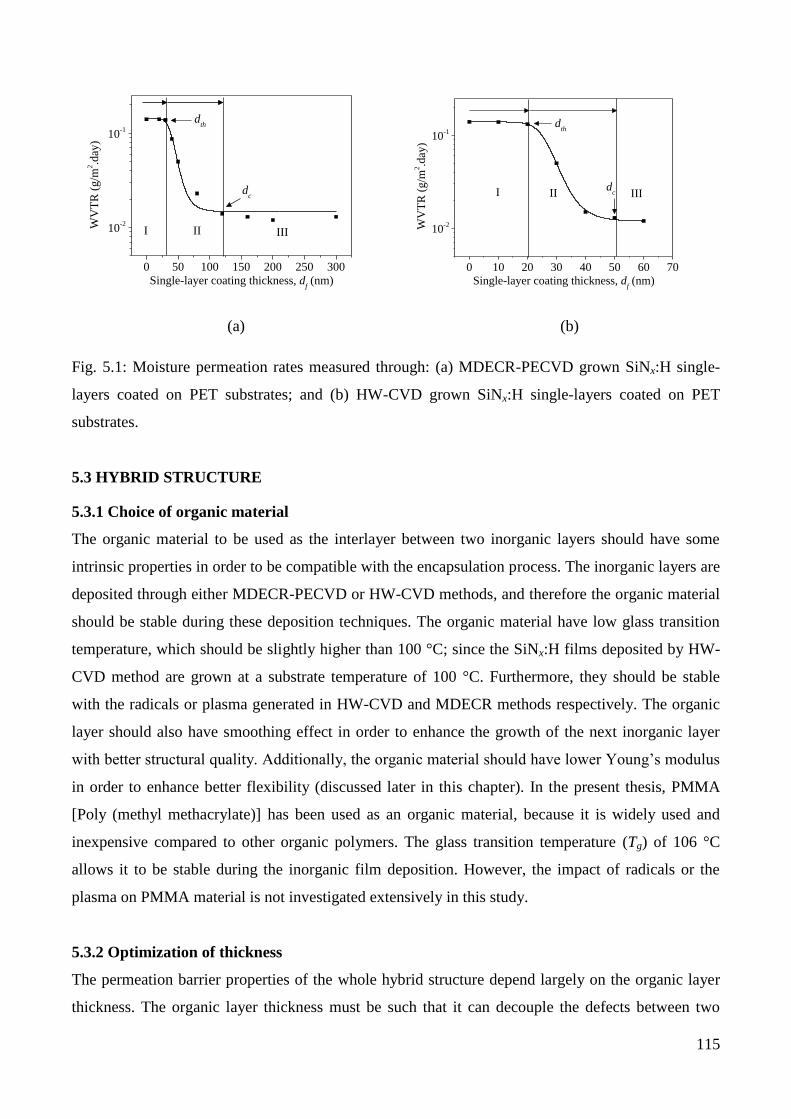
115
0 50 100 150 200 250 300
10-2
10-1
WV
TR
(g
/m2.d
ay)
Single-layer coating thickness, df (nm)
I II III
dth
dc
0 10 20 30 40 50 60 70
10-2
10-1
IIIII
WV
TR
(g
/m2.d
ay)
Single-layer coating thickness, df (nm)
I
dth
dc
(a) (b)
Fig. 5.1: Moisture permeation rates measured through: (a) MDECR-PECVD grown SiNx:H single-
layers coated on PET substrates; and (b) HW-CVD grown SiNx:H single-layers coated on PET
substrates.
5.3 HYBRID STRUCTURE
5.3.1 Choice of organic material
The organic material to be used as the interlayer between two inorganic layers should have some
intrinsic properties in order to be compatible with the encapsulation process. The inorganic layers are
deposited through either MDECR-PECVD or HW-CVD methods, and therefore the organic material
should be stable during these deposition techniques. The organic material have low glass transition
temperature, which should be slightly higher than 100 °C; since the SiNx:H films deposited by HW-
CVD method are grown at a substrate temperature of 100 °C. Furthermore, they should be stable
with the radicals or plasma generated in HW-CVD and MDECR methods respectively. The organic
layer should also have smoothing effect in order to enhance the growth of the next inorganic layer
with better structural quality. Additionally, the organic material should have lower Young’s modulus
in order to enhance better flexibility (discussed later in this chapter). In the present thesis, PMMA
[Poly (methyl methacrylate)] has been used as an organic material, because it is widely used and
inexpensive compared to other organic polymers. The glass transition temperature (Tg) of 106 °C
allows it to be stable during the inorganic film deposition. However, the impact of radicals or the
plasma on PMMA material is not investigated extensively in this study.
5.3.2 Optimization of thickness
The permeation barrier properties of the whole hybrid structure depend largely on the organic layer
thickness. The organic layer thickness must be such that it can decouple the defects between two

116
consecutive inorganic layers and thus create a tortuous diffusion path for the permeating water
molecules. According to Schaepkens et al. [102], the organic layer thickness is quite critical in
reducing the overall permeation barrier property. As shown in Fig. 5.2, whenever the interlayer
thickness is smaller than the average lateral distance between two consecutive defects, the
permeation rate reduces drastically. This is due to the fact that in this regime the permeation is no
longer Fickian diffusion, but one enters into the conduction limited diffusion. The ultrahigh barriers
should be in this regime. Although, in our present inorganic films, the exact defect density and defect
spacing are not extensively investigated, if realistic values are considered with a defect density of
100 defects/mm2 and consecutive defect spacing of 100 µm [102], it would be logical to have an idea
of the interlayer thickness.
Fig. 5.2: Dependence of interlayer thickness on overall permeation: (a) the interlayer thickness is
larger than the lateral distance between two consecutive defects; (b) the interlayer thickness is
smaller than the lateral distance between two consecutive defects and (c) ideal structure for ultrahigh
barrier coatings (note: the last structure is impossible to fabricate in practice, since the defect of the
underlying layer would propagate into the top layer). Reprinted with permission from [102].
Copyright 2004 American Vacuum Society.
117
To make alternating hard / soft structure, 300 nm polymer layers (PMMA) are deposited by spin-
coating technique inside the glove-box between two SiNx:H single-layers. The commercially
available PMMA is dissolved in chloroform (5 wt. %) and the solution is spin-coated on the already
grown SiNx:H film at 5000 rpm for 50 s followed by an annealing treatment at 100 °C for 30 min.
The thickness of the layer is measured by the Dektak 150 profilometer using the films coated on
Corning glass substrates. At least ten thickness measurements are taken on the film along the
centerline of the substrate. Fig. 5.3 shows the variation of PMMA layer thickness with spin-coater
speed.
0 1000 2000 3000 4000 5000 6000
200
400
600
800
Thic
knes
s (n
m)
Speed (rpm)
Fig. 5.3: Variation of PMMA film thickness with speed of the spin coater.
5.3.3 Surface morphology
The surface morphology of the as deposited and annealed PMMA films is analyzed by tapping mode
AFM technique. PMMA can be crystallized and become smoother when annealed near its glass
transition temperature (Tg) of 106 °C, as shown in Fig. 5.4. The average roughness of the PMMA
layer decreases 80% when it is annealed. The observed change in the morphology at the annealing
temperature of around 100 °C may be assigned to the reasons such as intensified thermal oscillations
of molecules at higher temperatures leading to the diminished order of their orientation, the improved
stoichiometry, reduction of defects and faster structural relaxation [208]. The surface topography of
the as deposited PMMA layer also shows some 50 nm diameter scale holes (in average) throughout
the surface. However, with the annealing of the layer the holes disappeared. This could be probably
due to the faster evaporation of the solvent when the sample is annealed. Structural modification of
the PMMA layer could help in hindering the propagation of any structural defects and producing the
subsequent inorganic layer with high quality.

118
(a) (b)
Fig. 5.4: The surface topography of the (a) as deposited PMMA film (Ravg. = 1.57 nm ); (b) PMMA
film annealed at 100 °C (Ravg. = 0.31 nm ).
5.3.4 Development of hybrid structure
An alternating layer structure is created consisting of an organic layer (PMMA) sandwiched between
two inorganic layers (SiNx:H), where the critical thickness (dc) is taken as a fixed parameter for
inorganic films, by making the moisture penetration path through the organic/inorganic interfaces
much longer and tortuous in order to improve the barrier performance. We prepared four different
structures of alternating barriers, as shown in Fig. 5.5, with increasing number of interfaces. The
interface between the first SiNx:H layer and the PET substrate is also counted. To check the
compatibility of both MDECR-PECVD and HW-CVD grown SiNx:H films and the spin-coated
PMMA films with the utilization in real optoelectronic devices, the optical transparency of the layers
is measured using the films grown on PET substrates. The reflectance and the transmittance spectra
are measured using Perkin Elmer Integrating Sphere.

119
Fig. 5.5: Schematic diagrams (not to scale) of 4 different permeation barrier hybrid structures with
different number of inorganic-organic interfaces. Here the thickness of SiNx:H layers is fixed at 50
nm. (a) 1 interface; (b) 3 interfaces; (c) 5 interfaces and (d) 7 interfaces.
SiNx:H
PET
SiNx:H
PET
SiNx:H
PMMA
(a) (b)
SiNx:H
PET
SiNx:H
PMMA
SiNx:H
PMMA
SiNx:H
PET
SiNx:H
PMMA
SiNx:H
PMMA
SiNx:H
PMMA
(c) (d)

120
5.4 HYBRID STRUCTURE WITH MDECR-PECVD GROWN SiNx:H
5.4.1 Optical properties of the hybrid structure
Figure 5.6 shows the reflectance and the transmittance measurement of the alternating layer structure
(stack of four 50 nm SiNx:H single-layers each separated by a 300 nm PMMA layer). The
transmittance curve indicates that the alternating layer structure is highly transparent (~ 80%) in one
part of the visible region (450 to 800 nm). It can also be seen from Fig. 5.6 that reflectance and
transmittance of this hybrid layer structure together are almost 100% in the range between 450 to 800
nm, meaning that some absorption takes place in the layers below 450 nm. In can be concluded that
even-though the increase of interfaces should logically improve the barrier properties, a trade-off
should be found between the permeation barrier properties and optical transparency taking into
account the number of interfaces.
300 400 500 600 700 800
0
20
40
60
80
100
Tra
nsm
itta
nce
/ R
efle
ctan
ce (
%)
Wavelength (nm)
Transmittance
Reflectance
Fig. 5.6: Reflection and transmission spectra of hybrid structure with 7 interfaces (stack of 4 SiNx:H
single-layers each separated by a PMMA layer).
5.4.2 Barrier properties of the hybrid structures
The evolutions of normalized conductance of the Ca sensors deposited on such hybrid-barrier coated
PET substrates are shown in Fig. 5.7 (a). When the number of SiNx:H / PMMA layers increases, the
number of interfaces between the organic and inorganic films increases as well. The water molecules
face a complex diffusion path when passing from one SiNx:H single-layer to the other through the
intermediate polymer layer (see Fig. 5.5). Due to that reason and to the increase in total thickness of
the coating, the minimum time taken by the water molecules to reach the Ca surface which is at the
opposite side of the coated PET substrates, increases with increasing number of interfaces. The
variation of “lag-time” with the increasing number of interfaces is shown in Fig. 5.7 (b) and a
maximum lag-time of 85 hours is achieved with 7 interfaces. The WVTR values also decreases with

121
increasing number of interfaces (see Fig. 5.7 (c)) and there is a significant drop of WVTR value
when the first PMMA layer is inserted between two 50 nm SiNx:H single-layers (3 hard/soft
interfaces), reaching down to 8 × 10⁻⁴
g/m2.day. This confirms the efficiency of the PMMA layer to
impede water vapour molecule diffusion. After that WVTR values decreases monotonically with
increasing number of interfaces reaching a minimum value of 2 × 10⁻⁴
g/m2.day for 7 interfaces,
which is quite sufficient for the requirement for the encapsulation of organic solar cells. However,
the barrier improvement factor (BIF) shown in Fig. 5.7 (d), clearly reveals that the impact of
additional interfaces beyond 3 interfaces of inorganic-organic is not quite efficient. Therefore, in
order to improve the barrier performance, either the quality of the inorganic/organic materials should
be improved, or a higher thickness of the inorganic layer (> critical thickness for MDECR) should be
used.
0 50 100 150 200 250 300 350 4000.0
0.2
0.4
0.6
0.8
1.0 1 interface
3 interfaces
5 interfaces
7 interfaces
No
rmal
ized
Co
nd
uct
ance
(S
)
Time (h)
1 2 3 4 5 6 70
20
40
60
80
100L
ag-t
ime
(h)
Number of interfaces
(a) (b)
1 2 3 4 5 6 7
10-4
10-3
10-2
10-1
WV
TR
(g
/m2.d
ay)
Number of interfaces
1 2 3 4 5 6 710
0
101
102
103
BIF
Number of interfaces
(c) (d)
Fig. 5.7: (a) Evolution of normalized conductance of the Ca sensor with time for different hybrid
structures deposited on PET with increasing number of interfaces. (b) Variation of lag-time with
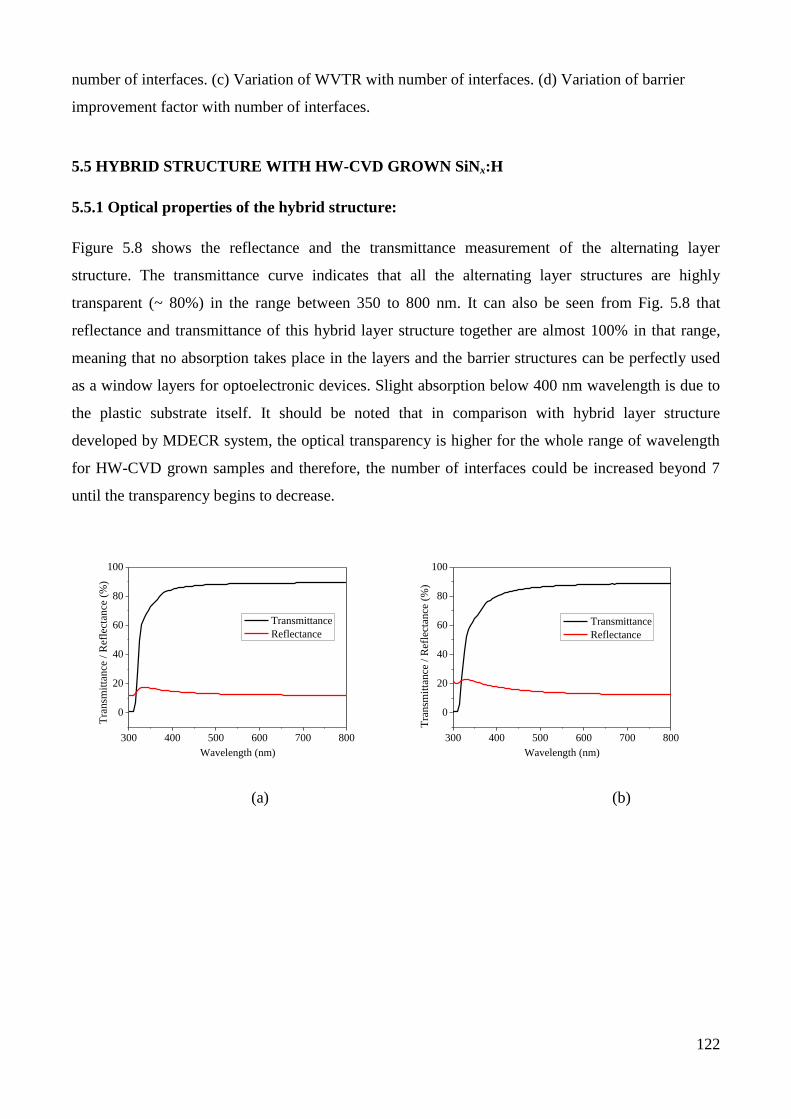
122
number of interfaces. (c) Variation of WVTR with number of interfaces. (d) Variation of barrier
improvement factor with number of interfaces.
5.5 HYBRID STRUCTURE WITH HW-CVD GROWN SiNx:H
5.5.1 Optical properties of the hybrid structure:
Figure 5.8 shows the reflectance and the transmittance measurement of the alternating layer
structure. The transmittance curve indicates that all the alternating layer structures are highly
transparent (~ 80%) in the range between 350 to 800 nm. It can also be seen from Fig. 5.8 that
reflectance and transmittance of this hybrid layer structure together are almost 100% in that range,
meaning that no absorption takes place in the layers and the barrier structures can be perfectly used
as a window layers for optoelectronic devices. Slight absorption below 400 nm wavelength is due to
the plastic substrate itself. It should be noted that in comparison with hybrid layer structure
developed by MDECR system, the optical transparency is higher for the whole range of wavelength
for HW-CVD grown samples and therefore, the number of interfaces could be increased beyond 7
until the transparency begins to decrease.
300 400 500 600 700 800
0
20
40
60
80
100
Tra
nsm
itta
nce
/ R
efle
ctan
ce (
%)
Wavelength (nm)
Transmittance
Reflectance
300 400 500 600 700 800
0
20
40
60
80
100
Tra
nsm
itta
nce
/ R
efle
ctan
ce (
%)
Wavelength (nm)
Transmittance
Reflectance
(a) (b)

123
300 400 500 600 700 800
0
20
40
60
80
100
Tra
nsm
itta
nce
/ R
efle
ctan
ce (
%)
Wavelength (nm)
Transmittance
Reflectance
(c)
Fig. 5.8: Reflection and transmission spectra of hybrid structures: (a) 3 interfaces; (b) 5 interfaces;
(c) 7 interfaces.
5.5.2 Barrier properties of the hybrid structures:
The evolutions of normalized conductance of the Ca sensors deposited on such hybrid-barrier coated
PET substrates are shown in Fig. 5.9 (a). The lag-time and WVTR values are assessed from the
evolution of the conductance and are shown in Fig. 5.9 (b) and (c). The results show a clear trend of
barrier improvement with an increasing number of interfaces. A maximum lag-time of 155 hours is
achieved with 7 interfaces. The WVTR value decreases with increasing number of interfaces and
there is a significant drop of WVTR value when the first PMMA layer is inserted between two 50 nm
SiNx:H single-layers (3 hard/soft interfaces), reaching down to 9.2 × 10⁻⁵
g/m2.day, confirming the
quality of PMMA as before. After that WVTR values decreases monotonically with increasing
number of interfaces reaching a minimum value of 4.5 × 10⁻⁵
g/m2.day for 7 interfaces. The barrier
improvement factor is one order of magnitude higher compared to the MDECR grown samples. As
the same organic layer (PMMA) is used to build the hybrid structures, therefore, the quality (the
deposition technique in other words) of the inorganic layers (SiNx:H) is quite critical in order to
improve the overall barrier performance.

124
0 400 800 1200 16000.0
0.2
0.4
0.6
0.8
1.0N
orm
aliz
ed c
on
du
ctan
ce (
S)
Time (h)
1 interface
3 interfaces
5 interfaces
7 interfaces
1 2 3 4 5 6 70
30
60
90
120
150
180
Lag
-tim
e (h
)
Number of interfaces
(a) (b)
1 2 3 4 5 6 7
10-4
10-3
10-2
WV
TR
(g
/m2.d
ay)
Number of interfaces
1 2 3 4 5 6 710
0
101
102
103
104
BIF
Number of interfaces
(c) (d)
Fig. 5.9: (a) Evolution of normalized conductance of the Ca sensor with time for different hybrid
structures deposited on PET with increasing number of interfaces. (b) Variation of lag-time with
number of interfaces. (c) Variation of WVTR with number of interfaces. (d) Variation of barrier
improvement factor with number of interfaces.
5.5.3 Mechanical property of the hybrid structures
The mechanical flexibility of the hybrid structure is investigated by bending a 3 interface structure
with a radius of curvature of 5 mm for different cycles of bending. Ca degradation tests are
performed on such deformed samples in order to assess the impact of bending on the permeation
barrier properties. It is quite obvious that when the samples are bent, due to the tensile stress channel
cracks are formed inside the inorganic films as shown in Fig. 2.12 in chapter 2. A good barrier
property of a structure depends on the ability of retaining the initial barrier properties even after
certain number of bending. In this section, such ability of the hybrid structure is discussed.

125
As discussed in chapter 4, when an inorganic film (in this case SiNx:H) is deposited on a pliable
under-layer (in this case PMMA), during deformation a tensile strain is induced inside the inorganic
layer. According to Yanaka et al. [190], onset strain for crack formation for thin inorganic films is
1.3%. In order to investigate the impact of bending on the induced strain inside the top inorganic
layer, the calculated variations of induced strains with radius of curvature, inter-layer (PMMA)
thickness and inter-layer’s Young’s modulus are shown in Fig. 5.10. When one parameter is
changed, other two parameters remain fixed. As shown in Fig. 5.10 (a), with the decrease of radius of
curvature (r); the induced strain inside the top inorganic SiNx:H layer increases. However, with very
serious bending (< 2 mm), the onset strain (1.3%) for cracking never reached. This is probably due to
the fact that during deformation, the soft under-layer (with lower Young’s modulus) of PMMA
absorbs the stress. The variation of the induced strain with increasing PMMA thickness is shown in
Fig. 5.10 (b): when the inter-layer thickness is increased, more strain is induced inside the top SiNx:H
layer. Therefore, the inter-layer thickness should be as small as possible. In the present study, a
PMMA thickness of 300 nm is used, which is a good approximation in order not to increase the
induced strain intensively. With the decrease of the inter-layer (PMMA) modulus, the induced strain
also decreases. This shows that the inter-layer material should be soft compared to the inorganic
barrier materials in order to develop a good barrier. In this case, the inter-layer material PMMA has a
modulus of 3.1 GPa, which is considerably small compared to the SiNx:H (297 GPa).
Fig. 5.11 (a) shows the Ca degradation test results after different number of bending cycles. The
black curve corresponds to the initial Ca test result without any bending. After that, the samples are
bent for 100 and 500 cycles respectively. The effect of bending on the lag-time is shown in Fig. 5.11
(b), which shows almost no change in lag-time even after 500 times of bending. Correspondingly, the
WVTR of the samples shows no change after 500 times of bending (Fig. 5.11 (c)). The observations
show that the hybrid structure can keep its moisture barrier properties even it is bent for several
times. It is worth mentioning that, the mechanical flexibility of the inorganic-organic hybrid structure
is much better compared to our other barrier structure (inorganic films with plasma surface
treatment).

126
(a)
(b)
0 2 4 6 8 10 12 14 16 18 200
0.001
0.002
0.003
0.004
0.005
0.006
0.007
0.008
0.009
0.01
Radius of curvature (mm)
Top layer
str
ain
(%
)
0 100 200 300 400 500 600 700 800 900 10000
0.5
1
1.5
2
2.5x 10
-3
Inter-layer thickness (nm)
Top layer
str
ain
(%
)

127
(c)
Fig. 5.10: Induced strain inside the top inorganic SiNx:H layer with the variation of (a) the radius of
curvature for a fixed inter-layer thickness and modulus; (b) inter-layer PMMA thickness for a fixed
inter-layer thickness and radius of curvature and (c) inter-layer modulus for a fixed thickness and
radius of curvature.
0 100 200 300 400 500 6000.0
0.2
0.4
0.6
0.8
1.0
No
rmal
ized
Co
nd
uct
ance
(S
)
Time (h)
No bending
100 times bending
500 times bending
0 100 200 300 400 5000
25
50
75
100
125
Lag
-tim
e (h
)
Number of bending
(a) (b)
0 50 100 150 200 250 300 350 400 450 5000
0.5
1
1.5
2
2.5
3
3.5
4
4.5
5x 10
-3
Inter-layer modulus (GPa)
Top layer
str
ain
(%
)

128
0 100 200 300 400 50010
-5
10-4
10-3
WV
TR
(g
/m2.d
ay)
Number of bending
(c)
Fig. 5.11: (a) Evolution of normalized conductance of the Ca sensor with time for hybrid structure
deposited on PET with different bending cycles. (b) Variation of lag-time with number of bending.
(c) Variation of WVTR with number of bending.
5.6 DISCUSSIONS ON BARRIER IMPROVEMENT
The above observed results can be interpreted qualitatively considering the different permeation
mechanisms and also processing conditions of hybrid structures. This conventional approach is a
well-established barrier structure which is already commercialized. Usually the permeation barrier
properties of the multilayer structures are explained by Ideal Laminate Theory (ILT) [209], which
actually corresponds to a series resistance model. The tortuous path model is also often used to
explain the permeation mechanism qualitatively. However, the impact of individual layers and the
quality of individual materials are not well understood.
The defect density of the inorganic layers and the defect size are probably the most important factor
which controls the water molecule permeation. In the present study, the impact of film quality in
terms of its density and stoichiometry on the overall barrier property is well demonstrated. However,
the lower barrier properties of MDECR grown films compared to HW-CVD films may not solely
depend on the quality of the films, but depend also on the defects created by the inner wall flakes or
dust particles, which is always the case for face-down deposition system. Since the MDECR is a
face-down deposition system, it is expected that the films grown have larger defect density compared
to face-up HW-CVD deposition system. Another technical problem arises from the sample handling.
Since the samples had to be transferred between reactor and the spin-coater system, there is a large
probability of dust particle contamination.

129
5.7 SUMMARY OF CHAPTER 5
i) The basic aim of this chapter is to fabricate ultrahigh barrier films using the conventional
inorganic-organic hybrid structures. Two different deposition techniques (MDECR-PECVD and
HW-CVD) are used to deposit the inorganic films, whereas the organic films are deposited by spin-
coating technique.
ii) The quality of the inorganic film is quite critical in order to achieve high barrier performance. The
density and the stoichiometry of the films affects largely on the overall permeation. Due to the higher
density and stoichiometry of the HW-CVD deposited films, the barrier properties are better
compared to MDECR-PECVD grown samples.
iii) The morphological property of the interlayer affects the overall barrier properties. The annealing
of the organic layer helps to develop a smoother layer which in turns helps to deposit the subsequent
inorganic layer with high structural quality.
iv) A minimum WVTR of 4.5 × 10⁻⁵
g/m2.day is achieved for 7 interfaces combining 4 HW-CVD
grown SiNx:H films and 3 spin-coated PMMA films. This value is one order of magnitude higher
than the requirement for organic LED devices. However, it can be utilized for the encapsulation of
organic solar cells.
v) Mechanical property of the hybrid structure is investigated thoroughly in order for their utilization
in flexible devices.

130
CHAPTER 6
ULTRA-BARRIER AND APPLICATION
6.1 INTRODUCTION
A perfect flexible encapsulation barrier should protect the degradable sensitive devices to attain a
shelf-lifetime of thousands of hours in operation, as well as provide flexibility to the whole device
system. The term ultra-barrier can be defined as a perfect barrier which has the lowest WVTR value
providing flexibility to the system. In the present thesis, two separate encapsulation strategies have
been developed and discussed which provided effective moisture barrier properties. Both strategies
gave rise to an effective WVTR of (4 - 7) × 10-5
g/m2.day. Although, the flexibility of the plasma
treated multi-barrier was not efficient, the other strategy consisting of hybrid organic-inorganic
layers showed excellent flexibility. The basic aim of this chapter is to combine the two strategies in
order to achieve improved barrier properties as well as higher flexibility of the whole system. The
last part of this chapter is devoted in fabricating real organic opto-electronic devices with the
encapsulation barriers to extend their shelf life-times.
6.2 COMBINED BARRIER STRUCTURE
The two different strategies discussed in the thesis, have been merged to develop an ultra-barrier
structure with the hope to reduce the water vapor diffusion drastically and capitalize the flexibility of
the soft organic layer between two inorganic layers. The ultra-barrier structure is shown in Fig. 6.1.
The structure consists of two 50 nm thick SiNx:H single-layers deposited by HW-CVD system with
the optimized growth conditions and both treated at the top surface by argon plasma with the
optimized treatment conditions (400 mW/cm2 power density, 25 mTorr pressure and 8 min duration).
The single-layers are separated by a spin-coated 300 nm thick PMMA layer as a soft interlayer. The
sample is deposited on clean PET substrate.

131
Fig. 6.1: Ultra-barrier structure (not to scale) consisting of two Ar plasma treated (30 eV) SiNx:H
single-layers (50 nm) separated by a soft PMMA (300 nm) layer deposited on PET substrate.
6.3 OPTICAL PROPERTIES
Optical transparency is an important parameter that defines the utilization of the barrier structure in
real electronic devices. The transparency of the barrier structure has been evaluated using the
integrating-sphere measurement. The transmittance (T) and the reflectance (R) of the sample are
shown in Fig. 6.2. The sample is highly transparent (> 80%) in the visible region. Slight absorption
below 400 nm is due to the plastic substrate itself as discussed before. This three layer barrier
structure can be perfectly used as window layer for organic electronic device, because almost no
absorption takes place in the visible region.
300 400 500 600 700 800 900 10000
20
40
60
80
100
Tra
nsm
itta
nce
/ R
efle
ctan
ce (
%)
Wavelength (nm)
Transmittance
Reflectance
Fig. 6.2: Transmittance and reflectance of the barrier structure in the visible region.
SiNx:H
SiNx:H
PET
PMMA (300 nm)
Ar treated
Ar treated
[ 50 nm
[ 50 nm

132
6.4 BARRIER PROPERTIES
The barrier properties have been assessed with the electrical calcium degradation test method. The
normalized conductance of the Ca sensor deposited on the other side of the barrier coated PET
substrate is shown in Fig. 6.3. The usual kinks can be observed in the traces, which arise due to
inhomogeneity inside the barrier as well as the substrate itself. The stable region of the evolution
which defines the minimum time taken by the water molecules to reach the calcium sensor (lag-time)
extends to ~420 h. This is the maximum lag-time value obtained in the present thesis. The
degradation of the calcium sensor extends to more than 3 months period. From a linear slope of the
degradation (just after the lag-time until the null value) the WVTR is assessed. A minimum WVTR
of ~6 × 10⁻⁶
g/m2.day has been obtained which is the lowest WVTR value achieved during the
present thesis. This result confirms the positive effect of the combination of the two different
encapsulation strategies and this tendency shows that if the number of layers is further increased, the
barrier properties will be possibly improved further.
0 400 800 1200 1600 2000 24000.0
0.2
0.4
0.6
0.8
1.0
Norm
aliz
ed c
onduct
ance
(S
)
Time (h)
Fig. 6.3: Normalized conductance of the Ca sensor deposited on the barrier coated PET substrate.
6.5 MECHANICAL PROPERTIES
The mechanical flexibility of the barrier structure has been investigated by bending the permeation
barrier with a radius of curvature of 5 mm for different cycles of bending. Ca degradation tests are
performed on such bent samples in order to assess the impact of bending on the permeation barrier
properties. Fig. 6.4 shows the Ca degradation test results relative to different bent samples after
several bending cycles. Both the barrier properties (lag-time and WVTR) show almost no
degradation even after 1000 bending cycles and thus confirming the viability of such barrier in real
flexible applications.

133
0 200 400 600 800 1000300
350
400
450
Lag-time
WVTR
Number of bending cycles
Lag
-tim
e (h
)10
-6
10-5
10-4
WV
TR
(g/m
2.d
ay)
Fig. 6.4: Variation of lag-time and WVTR with number of bending cycles.
6.6 DISCUSSIONS
There are two different strategies that affect the permeation of water molecules through the whole
barrier system. As discussed in chapter 4, the ionic bombardment with an energy of 30 eV impinging
on the SiNx:H film surface, rearrange the surface atoms locally and densify the surface up to few
nanometer (1.2 nm) in depth. The rearrangement of surface atoms also makes the SiNx:H surface
smoother and possibly reduces the number of micro or nano-voids. This rearrangement of atoms
blocks the propagation of water molecules through the SiNx:H single-layers hindering the native
nucleation centers which were existing at the top of the SiNx:H layers. The organic (PMMA)
interlayer in between two SiNx:H single-layers provides a planarization effect and decouples the
pinholes between two consecutive SiNx:H layers. The combination of those two strategies makes the
penetration path for water molecules much more complex and tortuous. Thus the effective diffusion
path of water molecules becomes longer which in turn is responsible for the excellent permeation
barrier properties.
6.7APPLICATION
The encapsulation barrier structures used in this thesis have been used to test the encapsulation
performance in real OLED devices. The OLED devices have been fabricated at the OLAE facility of
LPICM and their shelf life-times have been assessed using the barriers. The two best encapsulation
barriers obtained from the two different encapsulation strategies used in this thesis have been used
here. Encapsulation with a glass cover has been used as a reference.
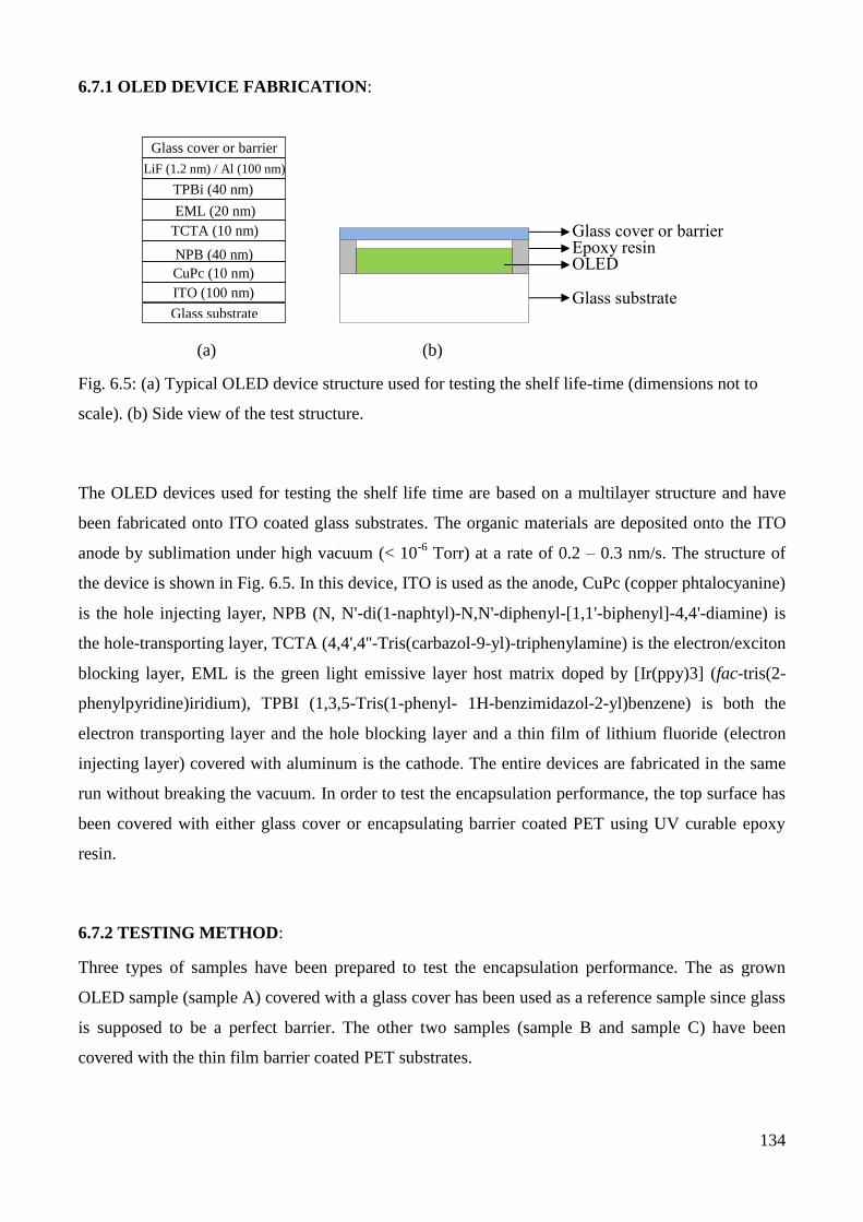
134
6.7.1 OLED DEVICE FABRICATION:
Fig. 6.5: (a) Typical OLED device structure used for testing the shelf life-time (dimensions not to
scale). (b) Side view of the test structure.
The OLED devices used for testing the shelf life time are based on a multilayer structure and have
been fabricated onto ITO coated glass substrates. The organic materials are deposited onto the ITO
anode by sublimation under high vacuum (< 10-6
Torr) at a rate of 0.2 – 0.3 nm/s. The structure of
the device is shown in Fig. 6.5. In this device, ITO is used as the anode, CuPc (copper phtalocyanine)
is the hole injecting layer, NPB (N, N'-di(1-naphtyl)-N,N'-diphenyl-[1,1'-biphenyl]-4,4'-diamine) is
the hole-transporting layer, TCTA (4,4',4''-Tris(carbazol-9-yl)-triphenylamine) is the electron/exciton
blocking layer, EML is the green light emissive layer host matrix doped by [Ir(ppy)3] (fac-tris(2-
phenylpyridine)iridium), TPBI (1,3,5-Tris(1-phenyl- 1H-benzimidazol-2-yl)benzene) is both the
electron transporting layer and the hole blocking layer and a thin film of lithium fluoride (electron
injecting layer) covered with aluminum is the cathode. The entire devices are fabricated in the same
run without breaking the vacuum. In order to test the encapsulation performance, the top surface has
been covered with either glass cover or encapsulating barrier coated PET using UV curable epoxy
resin.
6.7.2 TESTING METHOD:
Three types of samples have been prepared to test the encapsulation performance. The as grown
OLED sample (sample A) covered with a glass cover has been used as a reference sample since glass
is supposed to be a perfect barrier. The other two samples (sample B and sample C) have been
covered with the thin film barrier coated PET substrates.
Glass substrate
ITO (100 nm)
CuPc (10 nm)
NPB (40 nm)
TCTA (10 nm)
EML (20 nm)
TPBi (40 nm)
LiF (1.2 nm) / Al (100 nm)
Glass cover or barrier
Glass substrate
OLED Epoxy resin Glass cover or barrier
(a) (b)

135
Sample B Stack of 5 SiNx: H single layers each separated by Ar plasma treatment (30 eV), which
gave rise to WVTR of 7 × 10⁻⁵
g/m2.day (see chapter 4).
Sample C Stack of 4 SiNx: H single layers each separated by 300 nm PMMA layer, which gave
rise to WVTR of 4 × 10⁻⁵
g/m2.day (see chapter 5).
The luminance-current-voltage (L-I-V) characteristics of the devices have been measured with a
regulated power supply combined with a multimeter and a 1 cm2
area silicon calibrated photodiode.
The spectral emissions have been recorded with a Spectra Scan PR650 spectrophotometer. All the
measurements have been performed at room temperature and at ambient atmospheric conditions. The
bias current was set prior to the data collection in order to fix the OLED intensity at around 1000
cd/m2.
6.7.3 RESULTS AND DISCUSSIONS
The L-I-V characteristics of the as grown and the encapsulated OLED devices measured directly after
preparation are shown in Fig. 6.6. There are no significant differences in the electro-optical device
characteristics of the as grown and the encapsulated OLED devices. From this initial result, we can
conclude that there is no deterioration of the OLED characteristics even with encapsulation.
To verify the quality of the encapsulation layers, lifetime tests are carried out in constant current
mode at a starting luminance of 1000 cd/m2. We set the current density at 3 mA/cm
2 to measure the
luminance and the bias voltage at a regular time interval.
1 2 3 4 5 6 7 810
-1
100
101
102
No encapsulation
Sample A
Sample B
Sample C
No encapsulation
Sample A
Sample B
Sample C
Voltage (V)
Curr
ent
densi
ty (
mA
/cm
2)
0
5000
10000
15000
20000
Lum
inance (
cd/m
2)
Fig. 6.6: L-I-V characteristics of as grown and encapsulated OLEDs measured directly after
fabrication.

136
0 100 200 300 400 500 600 7000.0
0.2
0.4
0.6
0.8
1.0
luminance (sample A)
luminance (sample B)
luminance (sample C)
bias (sample A)
bias (sample B)
bias (sample C)
Time (h)
Lum
inan
ce (
Norm
aliz
ed)
Current density = 0.003 (A/cm2)
1.00
1.05
1.10
1.15
1.20
1.25
Bia
s (N
orm
aliz
ed)
Fig. 6.7: Lifetime characteristics (luminance and bias voltage) of the encapsulated OLED devices
(constant current mode).
The normalized luminance and the normalized bias voltage characteristics of the encapsulated OLED
devices are shown in Fig. 6.7. The OLED device without any encapsulation degraded very rapidly
(not shown in figure). Both characteristics show a constant luminance and bias values until 150 h
which is similar to the lag-time values obtained for those encapsulation barriers. The sample with
glass encapsulation also degrades after 150 h which is probably due to the residual gas volume in the
test structures. This is the drawback of this test set-up. In actual situations, the barriers should be
directly deposited on the OLED devices inside the vacuum chamber. The evolutions of the
normalized luminance values for all the above mentioned samples vary in a similar manner until the
lag-time value (150 h). Compared to the glass encapsulation, the OLEDs sealed with thin-film
barriers show a pronounced degradation after 150 h. The half-lifetime of all the OLED devices are
measured to be > 500 h, where the normalized luminance values degrade down to 0.5. From this test
results, we can conclude that our barriers imposed from the two different encapsulation strategies
show barrier properties nearly similar to hermetic sealing with glass encapsulation. This result is in
coherence with the Ca test result. In order to improve the shelf-lifetime of the OLEDs, the barriers
should be deposited directly on the OLED inside the vacuum chamber.

137
6.8 SUMMARY OF CHAPTER 6
i) An ultra-barrier layer structure has been developed combing two separate strategies as discussed in
chapter 4 and in chapter 5.
ii) The two strategies being compatible to each other provided excellent moisture permeation barrier
properties.
iii) A minimum WVTR of ~6 × 10⁻⁶
g/m2.day and an extended lag-time of ~420 h have been
obtained with this barrier structure.
iv) The barrier structure shows excellent flexibility even after 1000 bending cycles and thus
confirming the viability of this barrier in flexible applications.
v) We demonstrated the encapsulation barrier properties of the thin-film barriers fabricated by two
separate encapsulation strategies discussed in this thesis by utilizing the barriers on real OLED
devices.
vi) The thin-film barriers show good encapsulation behavior which evolves, in the first
approximation, in a similar way as the glass encapsulation. All the OLED samples showed an
extrapolated shelf-lifetime of > 500 h under ambient atmospheric conditions.

138
CHAPTER 7
CONCLUSIONS AND PERSPECTIVES
Several constraints must be addressed before successful commercialization of flexible organic
electronic devices like organic light emitting diode (OLED) and organic solar cells (OPV). The
requirement of an effective flexible encapsulation barrier is a critical one. The objective of the
research in this thesis has been the development of effective flexible encapsulation barrier layers for
organic electronic devices. A variety of challenges prevail for the development of effective
encapsulation barrier films such as, high optical transparency, low stress and low temperature
deposition in order to be compatible with the underlying polymer substrates. The appropriate choice
of the inorganic material as well as the deposition technique is critical in order to be congruent with
all the above mentioned limitations. SiNx:H film deposited by HW-CVD method was selected as the
inorganic permeation barrier material. The HW-CVD deposition method is advantageous compared
to the conventional plasma enhanced CVD deposition method because a lower concentration of H is
incorporated inside the films, leading to higher density films. ALD is an attractive method for
depositing barrier layers, even though the deposition rate is quite low. In order to synthesize the
permeation barriers, two separate ways have been adopted: either fabricating inorganic / inorganic
multilayer barriers separated by a plasma treated interface or fabricating inorganic / organic hybrid
multilayer moisture barriers.
The efforts of the present work have been focused on two main items: Firstly, the development of a
novel concept of encapsulation films other than the conventional approach of organic/inorganic
hybrid layer structures was imperative: this concept has consisted of deposition of insulating
multilayers separated by a plasma treatment. Secondly, the implementation of an accurate assessment
of the quality of the deposited permeation barrier layers: the measurement of permeation through the
use of the electrical calcium degradation test developed in our laboratory. This method is highly
sensitive and it has allowed measuring the WVTR rate below 10-6
g/ m2.day which is the requirement
for highly sensitive OLED devices. The WVTR results obtained from various measurements shows
the reproducibility and sensitivity (10-6
g/ m2.day with a standard deviation of 3.7%) of this tool.
Transparent and quasi-stoichiometric silicon nitride thin films have been deposited by HW-CVD
using silane and ammonia gaseous precursors, diluted in hydrogen, at a substrate temperature of 100
°C and with optimized growth parameters (filament current, flow rates, pressure). The evolution of

139
the lag-time and WVTR values with the increasing SiNx:H single-layer thickness have been observed
using the Ca degradation test in order to define the critical thickness of 50 nm. The critical thickness
is the optimal thickness above which both quantities do not improve anymore. This experimental
work has been followed by the development of multilayer stacks of SiNx:H single-layers, where the
thickness of each single-layer has been fixed at the critical thickness. Although the multilayer stack
of SiNx:H single-layers showed a slight improvement of the permeation barrier properties, the
WVTR improvement was clearly insufficient. Thus, a supplementary process was absolutely
necessary to reduce the diffusion of moisture drastically.
This process has been based on the combination of multilayer of SiNx:H, separated by intermediate
plasma treatments between the successive single-layers. The choices of Ar as species for the plasma,
treatment parameters and their optimizations have been crucial. The arduous part of the plasma
treatment was to modify the surface atom arrangement without disturbing the bulk. In order to
accurately reach this goal, several energy threshold values were taken into consideration, like surface
atomic displacement threshold, bulk atomic displacement threshold, sputtering energy threshold and
implantation threshold, which collectively determines the maximum ion bombardment energy
permissible for obtaining surface atomic rearrangement. The treatment power density, working
pressure and treatment duration were varied independently keeping the other parameters constant for
the combined effect of controlling the maximum ion bombardment energy on the film surface. The
treatment parameters were carefully chosen so that the maximum ion bombardment energy slightly
exceeded the bulk atomic displacement energy threshold, without damaging the barrier properties.
Two extreme treatment conditions were shown: a low energy treatment which had no significant
effect on the barrier properties and a high energy treatment which had deleterious effect on the
barrier properties. It has been shown in this dissertation that the accurate choice of the energy range
is noticeably limited in order to improve the performance.
Utilizing the optimized Ar treatment parameters between successive HW-CVD grown SiNx:H single-
layers, we reported extremely low WVTR values (7 × 10⁻⁵
g/m2.day). Compared to the conventional
procedures based on either hybrid structures of two different inorganic materials [84] or hybrid
structures of organic/inorganic materials [69], our encapsulation method has the merit of reducing
the efforts needed to get the permeation barrier quality of the same level as those obtained by hybrid
structures. Several intermediate characterizations have been performed to qualify and quantify the
results due to the ion induced surface modifications. Densification of the film up to few nanometers
in depth, reduction of micro-voids and smoothening of the surface explain indirectly the
improvement of barrier properties. Although, the measurement of the actual porosity of the films

140
without and with plasma treatment could make the explanation much more illuminating, it can be a
future characterization work continuing this dissertation. The dissertation shows that the
improvement of permeation barrier properties depends strongly on the precise range of low kinetic
energy (< 40 eV) of the bombarding ions. Therefore, a future research direction of this work could be
focused on studying the plasma treatment with tailored voltage waveform with a fixed maximum
energy, without applying a large distribution of ion energy used in the present study. Further
optimizations could be performed varying the bombarding energy step by step within the limit shown
in the thesis. Moreover few experiments have been carried out during the thesis with a plasma
treatment using low frequency plasma (100 kHz) and the permeation barrier properties improved
slightly compared to RF plasma used in this study (see Appendix A). However, due to some
technical issues, the optimizations were not performed thoroughly. Thus, it will be also interesting to
study the plasma treatment effects using low frequency (100 kHz) plasma, a frequency low enough
for the Ar+ ions to follow the variations of the electric field of the wave, so that the ions can gain
higher kinetic energy, thus decreasing the treatment duration.
The second part of this dissertation has been devoted to fabricating inorganic/organic hybrid layer
structure which is the conventional approach of developing encapsulation films. The quality of the
organic layer material is quite important in order to fabricate high quality barriers. The contribution
of the present thesis was based on improving the barrier properties by improving the organic-
inorganic interfaces, using simple deposition method (spin-coating) for the organic layer. Two
different techniques, MDECR-PECVD and HW-CVD, were used to deposit the SiNx:H single-layers
and their performances were compared. It was concluded that density and stoichiometry of the
inorganic material is critical to obtain efficient barrier layers. As a future research direction of this
approach, the processing steps could be minimized and the quality of the organic layer as well as
ability to deposit precise organic layer thickness should be taken into account. Spin-coating process
with reduced annealing time, initiated CVD method, ink-jet printing and spraying methods can be
some deposition solutions to process large area substrates.
Finally, it should be noted that the plasma treated inorganic multilayer structures or the organic-
inorganic hybrid barrier structures are not distinctive encapsulation fabrication solutions. Efforts
have been devoted to combine these two separate processes, which have drastic effect on the overall
barrier performance (WVTR = 6 × 10⁻⁶
g/m2.day) and showed better mechanical flexibility.
However, the processing steps should be minimized in order to be attractive for successful
commercialization.

141
Recently, graphene has shown permeation barrier properties towards atmospheric gases and this idea
has led to some basic studies performed during this dissertation to fabricate hybrid barrier layers by
combining commercially available monolayers of graphene and SiNx:H single-layers (thickness < 50
nm). The barrier performance improved slightly and further studies are required to develop this
method successfully (see Appendix B). Transparent hydrophobic clay can also be used as effective
permeation barrier layers, which will be an unusual process other than the conventional approaches.
The performance of the encapsulation techniques have been evaluated on real organic electronic
devices (OLEDs), which showed an extended shelf life-times for those devices. However for the
successful commercialization, integration of encapsulation films on real devices is one of the major
issues that should be solved in future research. When economically viable encapsulation solutions is
integrated on highly efficient organic electronic devices, the flexible electronics is expected to
overcome all the present device technologies.

142
REFERENCES
[1] (www.iea.org).
[2] N. Grossiord, J. M. Kroon, R. Andriessen, P. W.M. Blom, “Degradation mechanisms in organic
photovoltaic devices”, Organic Electronics, 13 (2012) 432-456.
[3] R. W. Bentley, “Global oil & gas depletion: an overview”, Energy Policy, 30 (2002) 189-205.
[4] R. A. Kerr, “How Urgent Is Climate Change”, Science, 318 (2007) 1230.
[5] A. Jäger-Waldau, PV Status Report 2003, European Commission (2003), EUR 20850 EN.
[6] W. A. Hermann, “Quantifying global energy resources, Energy, 31 (2006) 1685.
[7] J. Kalowekamo, E. Baker, “Estimating the manufacturing cost of purely organic solar cells”,
Solar Energy, 83 (2009) 1224-1231.
[8] G. Dennler, C. J. Brabec, Socio-economic I”mpact of Low Cost PV Technologies, in: C. J.
Brabec, V. Dyakonov, U. Scherf (Eds.), Organic Photovoltaics: Materials, Device Physics and
Manufacturing, Wiley VCH Verlag GmbH & Co., Weinheim, 2008.
[9] J. Schmidtke, “Commercial status of thin-film photovoltaic devices and materials”, Optics
Express, 18 (2010) A477-A486.
[10] C. K. Chiang, C. R. Fincher, Y. W. Park, A. J. Heeger, H. Shirakawa, E. J. Louis, S. C. Gau,
A. G. MacDiarmid, “Electrical Conductivity in Doped Polyacetylene”, Phys. Rev. Lett., 39
(1977) 1098.
[11] C. J. Brabec, J. A. Hauch, P. Schilinsky, C. Waldauf, “Production Aspects of Organic
Photovoltaics and Their Impact on the Commercialization of Devices”, MRS Bulletin, 30 (2005)
50-52.
[12] M. Stolka, “Organic Light Emitting Diodes (OLEDs) for General Illumination Update 2002”,
Optoelectronics Industry Development Association, Washington, DC 20036-4380, 2002.
[13] C. W. Tang, S. A. Vanslyke, “Organic electroluminescent diodes”, Appl. Phys. Lett., 51
(1987) 913-915.
[14] B. Geffroy, P. le Roy, C. Prat, “Organic light-emitting diode (OLED) technology: materials,
devices and display technologies”, Polym. Int., 55 (2006) 572-582.
[15] J. H. Burroughes, D. D. C. Bradley, A. R. Brown, R. N. Marks, K. Mackey, R. H. Friend, P.
L. Burns, A. B. Holmes, “Light emitting diodes based on conjugated polymers”, Nature, 347
(1990) 539-541.
[16] (http://www.clubic.com/actualite-74135-sony-ecran-oled-flexible-16-couleurs.html).
[17] (http://newenergyandfuel.com/http:/newenergyandfuel/com/2011/05/24/new-record-set-for-
flexible-solar-cells/).

143
[18] J. S. Lewis, M. S. Weaver, “Thin-Film Permeation-Barrier Technology for Flexible Organic
Light-Emitting Devices”, IEEE Journal of Selected Topics in Quantum Electronics, 10
(January/February 2004) No.1.
[19] D. Letian, Y. Jingbi, Y. Jun, C. Chun-Chao, H. Youjun, M. Seiichiro, M. Tom, E. Keith, L.
Gang, Y. Yang, “Tandem polymer solar cells featuring a spectrally matched low-band gap
polymer”. Nature Photonics, 6 (3) (2012) 180.
[20] J. Zhou, Y. Zuo, X. Wan, G. Long, Q. Zhang, W. Ni, Y. Liu, Z. Li, G. He, C. Li, B. Kan, M.
Li, Y. Chen, “Solution processed and high performance organic solar cells using small molecules
with a Benzodithiophene unit”, J. Am. Chem. Soc., 135 (2013) 8484.
[21] Y. Liu, C. –C. Chen, Z. Hong, J. Gao, Y. (Michael) Yang, H. Zhou, L. Dou, G. Li, Y. Yang,
“Solution processed small molecule solar cells : breaking the 10% power conversion efficiency”,
Scientific Reports, 3 (2013) 3356.
[22] J. Morgado, R. H. Friend, F.Cacialli, “Environmental aging of poly (p-phenylenevinylene)
based light emitting diodes”, Synt. Met., 114 (2000) 189-196.
[23] D. G. J. Sutherland, J. A. Carlisle, P. Elliker, G. Fox, T. W. Hagler, I. Jimenez, H. W. Lee, K.
Pakbaz, L. J. Terminello, S. C. Williams, F. J. Himpsel, D. K. Shuh, W. M. Tong, J. J. Jia, T. A.
Callcott, D. L. Ederer, “Photo-oxidation of electro-luminescent polymers studied by core-level
photoabsorption spectroscopy”, App. Phys. Lett., 68 (1996) 2046-2048.
[24] R. Scurlock, B. Wang, P. Ogilby, J. Sheats, R.Clough, “Singlet oxygen as a reactive
intermediate in the photo-degradation of an electroluminescent polymer”, J. Am. Chem. Soc. 117
(1995) 10194.
[25] S. Kumar, A. Biswas, V. Shukla, A. Awasthi, R. Anand, J. Narain, “Application of
spectroscopic ellipsometry to probe the environmental and photo-oxidative degradation of
poly(p-phenylene vinylene) (PPV)”, Synth. Met., 139 (2003) 751.
[26] H. Neugebauer, C. Brabec, J. Hummelen, N. Sariciftci, “Stability and photo-degradation
mechanisms of conjugated polymer/fullerene plastic solar cells”, Sol. Energy. Mat. Sol. Cells., 61
(2000) 35.
[27] F. Padinger, T. Fromherz, P. Denk, C.J. Brabec, J. Zettner, T. Hierl, N.S. Sariciftci,
“Degradation of bulk heterojunction solar cells operated in an inert gas atmosphere: a systematic
study”, Synth. Met., 121 (2001) 1605-1606.
[28] Y. C. Han, C. Jang, K. J. Kim, K. C. Choi, K. H. Jung, B. S. Bae, “The encapsulation of an
organic light emitting diode using organic-inorganic hybrid materials and MgO”, Organic
Electronics, 12 (2011), 609-613.
[29] S. Y. Kim, K. Y. Kim, Y. H. Tak, J. L. Lee, “Dark spot formation mechanism in organic light
emitting diode”, Appl. Phys. Lett., 89 (2006), 132108.

144
[30] P. Melpignano, A. Baron-Toaldo, V. Biondo, S. Priante, R. Zamboni, M. Murgia, S. Caria, L.
Gregoratti, A. Barinov, M. Kiskinova, “Mechanism of dark-spot degradation of organic light
emitting devices”, Appl. Phys. Lett., 86 (2005) 041105.
[31] Y. F. Liew, H. Aziz, N. X. Hu, H. S. O. Chan, G. Xu, Z. Popovic, “Investigation of the sites
of dark spots in organic light emitting devices”, Appl. Phys. Lett., 77 (2000) 2650.
[32] Jay Lewis, “Material challenges for flexible organic devices”, Materials Today, 9 (2006) 4.
[33] F. Papadimitrakopoulos, X. –M. Zhang, K. A. Higginson, “Chemical and Morphological
Stability of Aluminum Tris (8-Hydroxyquinoline) (Alq3): Effects in Light-Emitting Devices”,
IEEE J. Sel. Topics in Quantum Electronics, 4 (1998) 1.
[34] P. E. Burrows, G. L. Graff, M. E. Gross, P. M. Martin, M. Hall, E. Mast, C. C. Bonham, W.
D. Bennett, L. A. Michalski, M. S. Weaver, J. J. Brown, D. Fogarty, L. S. Sapochak, “Gas
permeation and lifetime tests on polymer-based barrier coatings”, Proc. SPIE, 4105 (2001) 75-
83.
[35] M. S. Weaver, L. A. Michalski, K. Rajan, M. A. Rothman, J. A. Silvernail, J. J. Brown, P. E.
Burrows, G. L. Graff, M. E. Gross, P. M. Martin, M. Hall, E. Mast, C. Bonham, W. Bennett, M.
Zumhoff, “Organic light emitting devices with extended operating lifetimes on plastic
substrates”, Appl. Phys. Lett., 81 (2002) 2929-2931.
[36] E. Guenther, R. S. Kumar, F. Zhu, H. Y. Low, K. S. Ong, M. D. Auch, K. Zhang, S. –J. Chua,
“Building blocks for ultra-thin, flexible organic electroluminescent devices”, Proc. SPIE, 4464
(2002) 23-33.
[37] G. Nisato, P. C. P. Bouten, P. J. Slikkerveer, W. D. Bennett, G. L. Graff, N. Rutherford, L.
Wiese, “Evaluating high performance diffusion barriers: The calcium test”, Proc. Int. Display
workshop/Asia Display, (2001) 1435-1438.
[38] G. Nisato, M. Kuilder, P. Bouten, “Thin film encapsulation for OLEDs: Evaluation of
multilayer barriers using the Ca test”, Proc. Soc. Inform. Display Symp. Dig. Tech. Papers, 34
(2003) 550-553.
[39] L. C. Olsen, S. N. Kundu, C. C. Bonham, M.Gross, “Barrier coatings for CIGSS and CdTe
cells”, Photovoltaics Specialists Conference, January 3–7, 2005, Conference Record of the
Thirty-First IEEE (2005) 327.
[40] J. Fahlteich, M. Fahland, W. Schönberger, N. Schiller, “Permeation barrier properties of thin
oxide films on flexible polymer substrates”, Thin Solid Films, 517 (2009) 3075-3080.
[41] International Electrotechnical Commission, IEC-61646- Thin film terrestrial photovoltaic
(PV) modules- design qualification and type approval (1997).
145
[42] G. Dennler, C. Lungenschmied, H. Neugebauer, N.S. Sariciftci, M. Latrèche, G.
Czeremuszkin, M.R. Wertheimer, “A new encapsulation solution for flexible organic solar cells”,
Thin Solid Films, 511-512 (2006) 349-353.
[43] J. A. Hauch, P. Schilinsky, S. A. Choulis, S. Rajoelson, C. J. Brabec, “The impact of water
vapor transmission rate on the lifetime of flexible polymer solar cells”, Appl. Phys. Lett., 93
(2008) 103306.
[44] S. Cros, R. de Bettignies, S. Berson, S. Bailly, P. Maisse, N. Lemaitre, S. Guillerez,
“Definition of encapsulation barrier requirements: A method applied to organic solar cells”, Sol.
Energy Mater. Sol. Cells, 95 (2011) S65.
[45] K. Zhang, F. R. Zhu, C. H. A. Huan, A. T. S. Wee, “Indium tin oxide films prepared by radio
frequency magnetron sputtering method at a low processing temperature”, Thin Solid Films, 376
(2000) 255-263.
[46] S. Angiolini, M. Avidano, C. Bracco, C. Barlocco, R. Bracco, J. Bacskay, J. –H. Lipian, P. S.
Neal, L. S. Rhodes, R. A. Shick, X. –M. Zhao, G. Freeman, “High performance plastic substrates
for flexible flat panel display”, Society For Information Display, Digest of Technical Papers, 1-4,
2000.
[47] AQUATRAN Model 1, Mocon, Minneapolis MN 55428, 2006.
[48] C. Charton, N. Schiller, M. Fahland, A. Hollander, A. Wedel, K. Noller, “Development of
high barrier films on flexible polymer substrates”, Thin Solid Films, 502 (2006) 99-103.
[49] J. –S. Park, H. Chae, H. K. Chung, S. I. Lee, “Thin film encapsulation for flexible AM-
OLED: a review”, Semicond. Sci. Technol., 26 (2011) 034001.
[50] R. S. Kumar, M. Auch, E. Ou, E. Guenther, S. –J. Chua, “Low moisture permeation
measurement through polymer substrates for organic light emitting devices”, Thin Solid Films,
417 (2002) 120-126.
[51] R. Paetzold, A. Winnacker, D. Henseler, V. Cesari, K. Heuser, “Permeation rate
measurements by electrical analysis of calcium corrosion”, Rev. Sci. Instrum., 74 (2003) 5147.
[52] P. F. Carcia, R. S. McLean, M. H. Reilly, M. D. Groner, S. M. George, “Ca test of Al2O3 gas
diffusion barriers grown by atomic layer deposition on polymers”, Appl. Phys. Lett., 89 (2006)
031915.
[53] S. Cros, M. Firon, S. Lenfant, P. Trouslard, L. Beck, “Study of thin calcium electrode
degradation by ion beam analysis”, Nuclear Instruments and Methods in Physics Research B, 251
(2006) 257.
[54] J. H. Choi, Y. M. Kim, Y. W. Park, J. W. Huh, B. K. Ju, I. S. Kim, H. N. Hwang, “Evaluation
of gas permeation barrier properties using electrical measurements of calcium degradation”, Rev.
Sci. Instrum., 78 (2007) 064701.
146
[55] P. F. Carcia, R. S. McLean, M. H. Reilly, “Permeation measurements and modeling of highly
defective Al2O3 thin films grown by atomic layer deposition on polymers”, Appl. Phys. Lett., 97
(2010) 221901.
[56] M. O. Reese, A. A. Dameron, M. D. Kempe, “Quantitative calcium resistivity based method
for accurate and scalable water vapor transmission rate measurement”, Rev. Sci. Instrum., 82
(2011) 085101.
[57] S. Schubert, H. Klumbies, L. Muller-Meskamp, K. Leo, “Electrical calcium test for moisture
barrier evaluation for organic devices ”, Rev. Sci. Instrum., 82 (2011) 094101.
[58] E. H. Song, Y. W. Park, J. H. Choi, T. H. Park, J. W. Jeong, H. Ju. Choi, B. K. Ju, “The
flexible Ca-test: An improved performance in a gas permeability measurement system”, Rev. Sci.
Instrum., 82 (2011) 054702.
[59] M. D. Kempe, M. O. Reese, A. A. Dameron, “Evaluation of the sensitivity limits of water
vapor transmission rate measurements using electrical calcium test”, Rev. Sci. Instrum., 84 (2013)
025109.
[60] S. Majee, M. F. Cerqueira, D. Tondelier, B. Geffroy, Y. Bonnassieux, P. Alpuim, J. E.
Bourée, “The Effect of Argon Plasma Treatment on the Permeation Barrier Properties of Silicon
Nitride Layers”, Surf. Coatings Technol., 235 (2013) 361.
[61] S. Majee, M. F. Cerqueira, D. Tondelier, B. Geffroy, Y. Bonnassieux, P. Alpuim, J. E.
Bourée, “Influence of Low Energy Ar Plasma Treatment on the Moisture Barrier Performance of
Hot Wire -CVD Grown SiNx Multilayers”, Japaneese Journal of Applied Physics, 53 (2014)
05FM05.
[62] S. Majee, M. F. Cerqueira, D. Tondelier, B. Geffroy, Y. Bonnassieux, P. Alpuim, J. E.
Bourée, “Permeation barrier performance of HW-CVD grown silicon nitride films treated by
argon plasma”, Thin Solid Films, (accepted).
[63] M. D. Groner, S. M. George, R. S. McLean, P. F. Carcia, “Gas diffusion barriers on polymers
using Al2O3 atomic layer deposition”, Appl. Phys. Lett., 88 (2006) 051907.
[64] A. R. Coulter, R. A. Deeken, G. M. Zentner, “Water permeability in poly(ortho ester)s”, J.
Membrane Sci., 65, 269.
[65] C. M. Hansen, L. Just, “Water transport and condensation in fluoro-polymer films”, Prog.
Org. Coat., 142 (2001) 167–178.
[66] W. Prins, J. J. Hermans, “Theory of Permeation through Metal Coated Polymer Films”, J.
Phys. Chem., 63 (1959) 716.
[67] T. A. Beu, P.-V. Mercea, D. Silipas, “Gas transport through metallized polymer membranes”,
Mater. Chem. Phys., 26 (1990) 309.

147
[68] S. da Silva Sobrinho, G. Czeremuszkin, M. Latrèche, M. R. Wertheimer, “Defect-permeation
correlation for ultrathin transparent barrier coatings on polymers”, J. Vac. Sci. Technol. A, 18
(2000) 149.
[69] D. Spee, K. van der Werf, J. Rath, R. Schropp, “Excellent organic/inorganic transparent thin
film moisture barrier entirely made by hot wire CVD at 100 °C”, Phys. Status Solidi: Rapid Res.
Lett., 6 (2012) 151–153.
[70] A. P. Roberts, B. M. Henry, A. P. Sutton, C. R. M. Grovenor, G. A. D. Briggs, T. Miyamoto,
M. Kano, Y. Tsukahara, M. Yanaka, “Gas permeation in silicon-oxide / polymer (SiOx / PET)
barrier films: role of the oxide lattice, nano-defects and macro-defects”, Journal of Membrane
Science, 208 (2002) 75-88.
[71] Yves Leterrier, “Durability of nanosized oxygen-barrier coatings on polymers”, Progress in
Materials Science, 48 (1) (2003) 1-55.
[72] A. S. da Silva Sobrinho, M. Latrèche, G. Czeremuszkin, J. E. Klemberg-Sapieha, and M. R.
Wertheimer, “Transparent barrier coatings on polyethylene terephthalate by single and dual
frequency plasma enhanced chemical vapour deposition”, J. Vac. Sci. Technol. A, 16 (1998)
3190.
[73] W. Huang, X. Wang, M. Sheng, L. Xu, F. Stubhan, L. Luo, T. Feng, X. Wang, F. Zhang, S.
Zou, “Low temperature PECVD SiNx films applied in OLED packaging”, Materials Science and
Engineering: B, 98 (2003) 248-254.
[74] P. Mandlik, J. Gartside, L. Han, I-C. Cheng, S. Wagner, J. A. Silvernail, R. –Q. Ma, M. Hack,
J. J. Brown, “A single layer permeation barrier for organic light emitting displays”, Appl. Phys.
Lett., 92 (2008) 103309.
[75] S. –H. K. Park, J. Oh, C. –S. Hwang, J. –I. Lee, Y. S. Yang, H. Y. Chu, K. –Y. Kang.,
“Ultra-thin film encapsulation of organic light emitting diode on a plastic substrate”, ETRI
Journal, 27 (2005) 545-550.
[76] W. J. Potscavage, S. Yoo, B. Domercq, B. Kippelen, “Encapsulation of pentacene/ C60
organic solar cells with Al2O3 deposited by atomic layer deposition”, Appl. Phys. Lett., 90 (2007)
253511.
[77] A. P. Ghosh, L. J. Gerenser, C. M. Jarman, and J. E. Fornalik, “Thin film encapsulation of
organic light emitting devices”, Appl. Phys. Lett., 86 (2005) 223503.
[78] Y. –Q. Yang, Y. Duan, P. Chen, F. –B. Sun, Y. –H. Duan, X. Wang, D. Yang, “Realization of
Thin Film Encapsulation by Atomic Layer Deposition Al2O3 at Low Temperature”, J. Phys.
Chem. C, 117(39) (2013) 20308-20312.
[79] S. –W. Seo, E. Jung, C. Lim, H. Chae, S. M. Cho, “Moisture permeation through ultrathin
TiO2 films grown by atomic layer deposition”, Appl. Phys. Exp., 5 (2012) 035701.

148
[80] H. Matsumura, “Silicon nitride produced by catalytic chemical vapor deposition method”, J.
Appl. Phys., 66 (1989) 3612.
[81] H. Matsumura, H. Umemoto, A. Izumi, A. Masuda, “Recent progress of Cat-CVD research in
Japan—bridging between the first and second Cat-CVD conferences”, Thin Solid Films, 430
(2003) 7.
[82] A. Masuda, M. Totsuka, T. Oku, R. Hattori, H. Matsumura, “Highly moisture-resistive silicon
nitride films prepared by catalytic chemical vapor deposition and application to gallium arsenide
field-effect transistors”, Vacuum, 74 (2004) 525.
[83] A. Heya, T. Niki, Y. Yonezawa, T. Minamikawa, S. Muroi, A. Izumi, A. Masuda, H.
Umemoto, H. Matsumura, “Highly Moisture-Resistive SiNx Films Prepared by Catalytic
Chemical Vapor Deposition”, Jpn. J. Appl. Phys., 43 (2004) 1362.
[84] Y. Ogawa, K. Ohdaira, T. Oyaidu, H. Matsumura, “Protection of organic light-emitting
diodes over 50 000 hours by Cat-CVD SiNx/SiOxNy stacked thin films”, Thin Solid Films, 516
(2008) 611.
[85] A. Heya, T. Minamikawa, T. Niki, S. Minami, A. Masuda, H. Umemoto, N. Matsuo, H.
Matsumura, “Cat-CVD SiN passivation films for OLEDs and packaging”, Thin Solid Films, 516
(5) (2008) 553-557.
[86] P. Alpuim, L. M. Gonçalves, E. S. Marins, T .M. R. Viseu, S. Ferdov, J. E. Bourée,
“Deposition of silicon nitride thin films by hot-wire CVD at 100 °C and 250 °C”, Thin Solid
Films, 517 (2009) 3503.
[87] H. –K. Kim, M. S. Kim, J. –W. Kang, J. –J. Kim, M. –S. Yi, “High-quality thin-film
passivation by catalyser-enhanced chemical vapour deposition for organic light-emitting diodes”,
Appl. Phys. Lett., 90 (2007) 013502.
[88] K. Saitih, R. S. Kumar, S. Chua, A. Masuda, H. Matsumura, “Estimation of moisture barrier
ability of thin SiNx single layer on polymer substrates prepared by Cat-CVD method”, Thin Solid
Films, 516 (2008) 607-610.
[89] H. Nakayama, M. Ito, “Super H2O-barrier film using Cat-CVD (HWCVD)-grown SiCN for
film based electronics”, Thin Solid Films, 519 (2011) 4483-4486.
[90] C.C. Chiang, D.S. Wuu, H.B. Lin, Y.P. Chen, T.N. Chen, Y.C. Lin, C.C. Wu, W.C. Chen,
T.H. Jaw, R.H. Horng, “Deposition and permeation properties of SiNX/parylene multilayers on
polymeric substrates”, Surface and Coatings Technology, 200 (2006) 5843-5848.
[91] T. –N. Chen, D. –S. Wuu, C. –C. Wu, C. –C. Chiang, Y. –P. Chen, R. –H. Horng,
“Improvements of Permeation Barrier Coatings Using Encapsulated Parylene Interlayers for
Flexible Electronic Applications”, Plasma Processes and Polymers, 4 (2007) 180.

149
[92] A. B. Chwang, M. A. Rothman, S. Y. Mao, R. H. Hewitt, M. S. Weaver, J. A. Silvernail, K.
Rajan, M. Hack, J. J. Brown, X. Chu, L. Moro, T. Krajewski, N. Rutherford, “Thin film
encapsulated flexible organic electroluminescent displays”, Appl. Phys. Lett., 83 (2003) 413.
[93] T. W. Kim, M. Yan, A. G. Erlat, P. A. McConnelee, M. Pellow, J. Deluca, T. P. Feist, A. R.
Duggal, M. Schaepkens, “Transparent hybrid inorganic/organic barrier coatings for plastic
organic light emitting diode substrates”, J. Vac. Sci. Technol. A, 23 (2005) 971.
[94] M. Yan, T. Wonkim, A. G. Erlat, M. Pellow, D. F. Foust, J. Liu, M. Schaepkens, C. M.
Heller, P. A. McConnelee, T. P. Feist, A. R. Duggal, “A transparent, high barrier and high heat
substrate for organic electronics”, Proc. IEEE, 93 (2005) 1468.
[95] S. Ramadas, “Ultra-High-Barrier Films for Solar, Display and Plastic Electronics
Applications”, Future Photovoltaics, August 2011.
[96] K. Akedo, A. Miura, H. Fujikawa, Y. Taga, “Plasma-CVD SiNx / plasma-polymerized CNx:H
multi-layer passivation films for organic light emitting diodes”, Proc. Soc. Inform. Display
Symp., Dig. Tech. Papers, 34 (2003) 559-561.
[97] C. Lungenschmied, G. Dennler, H. Neugebauer, S. N. Sariciftci, M. Glatthaar, T. Meyer, A.
Meyer, “Flexible, long-lived, large-area, organic solar cells”, Solar Energy Materials and Solar
Cells, 91 (2007) 379-384.
[98] A. Yoshida, A. Sugimoto, T. Miyadera, S. Miyaguchi, “Organic light emitting devices on
polymer substrates”, J. Photopolymer Sci. Technol., 14 (2001) 327-332.
[99] S. –W. Seo, E. Jung, H. Chae, S. M. Cho, “Optimization of Al2O3/ZrO2 nanolaminate
structure for thin film encapsulation of OLEDs”, Organic Electronics, 13 (2012) 2436-2441.
[100] S. –W. Seo, H. Chae, S. J. Seo, H. K. Chung, S. M. Cho, “Extremely bendable thin-film
encapsulation of organic light emitting diodes”, Appl. Phys. Lett., 102 (2013) 161908.
[101] E. Kim, Y. Han, W. Kim, K. C. Choi, H. –G. Im, B. –S. Bae, “Thin film encapsulation for
organic light emitting diodes using a multi-barrier composed of MgO prepared by atomic layer
deposition and hybrid materials”, Organic Electronics, 14 (2013) 1737-1743.
[102] M. Schaepkens, T. W. Kim, A. G. Erlat, M. Yan, K. W. Flanagan, C. M. Heller, P. A.
McConnelee, “Ultrahigh barrier coating deposition on polycarbonate substrates”, J. Vac. Sci.
Technol. A, 22 (2004) 1716.
[103] A. Hofrichter, P. Bulkin, B. Drévillon, “Plasma enhanced chemical vapour deposition of
SiOxNy in an integrated distributed electron cyclotron resonance reactor”, Appl. Surf. Sci., 142
(1999) 447.
[104] R. Botha, B. Haj Ibrahim, P. Bulkin, B. Drévillon, “Deposition of dielectrics using a matrix
distributed electron cyclotron resonance plasma enhanced chemical vapor deposition system”,
Thin Solid Films, 515 (2007) 7594–7597.

150
[105] R. Botha, Ph.D. thesis, Ecole Polytechnique, France, 2008. (http://tel.archives-
ouvertes.fr/docs/00/50/37/45/PDF/Botha.pdf).
[106] M. Yasaka, “X-ray thin film measurement techniques”, The Rigaku Journal, 26 (2010) 2.
[107] L. G. Parratt, “Surface studies of solids by total reflection of X-rays”, Phys. Rev., 95 (1954) 2.
[108] S. W. Schmitt, G. Gamez, V. Sivakov, M. Schubert, S. H. Christiansen, J. Michler,
“Chemical and optical characterisation of atomic layer deposition aluminium doped ZnO films
for photovoltaics by glow discharge optical emission spectrometry”, J. Anal. At. Spectrom., 26
(2011) 822-827.
[109] B. Ber, P. Bábor, P.N. Brunkov, P. Chapon, M.N. Drozdov, R. Duda, D. Kazantsev, V.N.
Polkovnikov, P. Yunin, A. Tolstogouzov, “Sputter depth profiling of Mo/B4C/Si and Mo/Si
multilayer nanostructures: A round-robin characterization by different techniques”, Thin Solid
Films, 540 (2013) 96–105.
[110] B. Drévillon, “Phase modulated ellipsometry from the ultraviolet to the infrared: In situ
application to the growth of semiconductors”, Prog. Cryst. Growth Char. Mat., 27 (1993) 1.
[111] R. Azzam, N. Bashara, “Ellipsometry and polarized light”, North Holland Personal Library
(1970).
[112] S.N. Jasperson, D.K. Burge, R.C. O’Handley, “A modulated ellipsometer for studying thin
film optical properties and surface dynamics”, Surface Science, 27 (1973) 548.
[113] F. Abelès, “Recherches sur la propagation des ondes électromagnétiques sinusoïdales dans les
milieux stratifiés. Application aux couches minces”, Annales de Physique, 5 (1950) 596 (706).
[114] D.A.G. Bruggeman, “Berechnung verschiedener physikalischer Konstanten von
heterogenen Substanzen”, Ann. Physik, Leipzig, Germany, 24 (1935) 636.
[115] M. Stchakovsky, C. Caillaud, M. Foldyna, R. Ossikovski, E. Garcia-Caurel, “Polarimetric
characterization of optically anisotropic flexible substrates”, Thin Solid Films, 516 (2008) 1414-
1418.
[116] S. W. Rutherford, D. D. Do, “Review of time lag permeation technique as a method for
characterization of porous media and membranes”, Adsorption, 3 (1997) 283-312.
[117] G. L. Graff, R. E. Williford, P. E. Burrows, “Mechanics of vapor permeation through
multilayer barrier films: Lag time versus equilibrium permeation”, Journal of Applied Physics,
96 (2004) 4.
[118] F.M.Smits, “Measurement of Sheet Resistivities with the Four-Point Probe,” The Bell
System Technical Journal, 37 (1958) 711-718.
[119] Z. Jia, M. B. Tucker, T. Li, “Failure mechanics of organic-inorganic multilayer permeation
barriers in flexible electronics”, Composites Science and Technology, 71 (2011) 365-372.
151
[120] A. Masuda, H. Umemoto, H. Matsumura, “Various applications of silicon nitride by
catalytic chemical vapor deposition for coating, passivation and insulating films”, Thin Solid
Films, 501 (2006) 149-153.
[121] A. Shah, “Thin-film silicon solar cells”, EPFL Press, Lausanne, Switzerland, 2010.
[122] H. Matsumura, K. Ohdaira, “Recent situation of industrial implementation of Cat-CVD
technology in Japan”, Thin Solid Films, 516 (2008) 537-540.
[123] S. Asari, T. Fujinaga, M. Takagi, M. Hashimoto, K. Saito, M. Harada, M. Ishikawa,
“ULVAC research and development of Cat-CVD applications”, Thin Solid Films, 516 (2008)
541-544.
[124] T. Oku, Y. Kamo, M. Totsuka, “AlGaN/GaN HEMTs passivated by Cat-CVD SiN Film”,
Thin Solid Films, 516 (2008) 545-547.
[125] T. Osono, A. Heya, T. Niki, M. Takano, T. Minamikawa, S. Muroi, A. Masuda, H.
Umemoto, H. Matsumura, “High-rate deposition of SiNx films over 100 nm/min by Cat-CVD
method at low temperatures below 80 °C”, Thin Solid Films, 501 (2006) 55-57.
[126] V. Verlaan, Z. S. Houweling, C. H. M. van der Werf, I. G. Romijn, A. W. Weeber, H. D.
Goldbach, R. E. I. Schropp, “Deposition of device quality silicon nitride with ultra-high
deposition rate (>7 nm/s) using hot-wire CVD”, Thin Solid Films, 516 (2008) 533-536.
[127] C. Niikura, “Microcrystalline silicon films prepared by hot–wire assisted catalytic chemical
vapor deposition: from analysis of film properties to realization of solar cells”, PhD thesis, Ecole
Polytechnique, Palaiseau Cedex, France (2002).
[128] K. Honda, K. Ohdaira, H. Matsumura, “Study of silicidation process of Tungsten catalyzer
during silicon film deposition in catalytic chemical vapor deposition”, Jpn. J. Appl. Phys., 47
(2008) 3692-3698.
[129] J. E. Bourée, J. Guillet, C. Grattepain, J. Chaumont, “Quantitative analysis of tungsten,
oxygen and carbon concentrations in the microcrystalline silicon films deposited by hot wire
CVD”, Thin Solid Films, 430 (2003) 110-115.
[130] P. A. T. T. van Veenendaal, O. L. J. Gijzeman, J. K. Rath, R. E. I. Schropp, “The influence of
different catalyzers in hot-wire CVD for the deposition of polycrystalline silicon thin films”, Thin
Solid Films, 395 (2001) 194-197.
[131] A. Pflüger, C. Mukherjee, B. Schröder, “Optimization of process parameters in a large-area
hot-wire CVD reactor for the deposition of amorphous silicon (a-Si:H) for solar cell application
with highly uniform material quality”, Solar Energy Materials and Solar Cells, 73 (2002) 321-
337.
[132] A. Heya, PhD Thesis, Japan Advanced Institute of Science and Technology, Japan (2000).

152
[133] K. F. Feenstra, R. E. I. Schropp, W. F. van der Weg, “Deposition of amorphous silicon films
by hot-wire chemical vapour deposition”, Journal of Applied Physics, 85 (1999) 6843.
[134] E. C. Molenbroek, A. H. Mahan, A. Gallagher, “Mechanisms influencing “hot-wire”
deposition of hydrogenated amorphous silicon”, J. Appl. Phys., 82 (1997) 1909.
[135] J. E. Bourée, S. R. Jadkar, S. Kasouit, R. Vanderhaghen, “Transport in microcrystalline
silicon thin films deposited at low temperature by hot-wire chemical vapour deposition”, Thin
Solid Films, 501 (2006) 133-136.
[136] K. Yasui, H. Katoh, K. Komaki, S. Kaneda, “Amorphous SiN films grown by hot‐filament
chemical vapor deposition using monomethylamine”, Appl. Phys. Lett., 56 (1990) 898.
[137] J. L. Dupuie, E. Gulari, F. Terry, “The Low Temperature Catalyzed Chemical Vapor
Deposition and Characterization of Silicon Nitride Thin Films”, J. Electrochem. Soc., 139(4)
(1992) 1151-1159.
[138] S. Okada, H. Matsumura, “Improved properties of silicon nitride films prepared by the
catalytic chemical vapor deposition method”, Jpn. J. Appl. Phys., 36 (1997) 7035-7040.
[139] B. P. Nelson, Q. Wang, E. Iwaniczko, A. H. Mahan, R. S. Crandall, “The Influence of
Electrons From the Filament on the Material Properties of Hydrogenated Amorphous Silicon
Grown by the Hot-Wire Chemical Vapor Deposition Technique”, Mater. Res. Soc. Symp. Proc.,
507 (1998) 927.
[140] Q. Wang, S. Ward, L. Gedvilas, B. Keyes, E. Sanchez, S. Wang, “Conformal thin-film silicon
nitride deposited by hot-wire chemical vapor deposition”, Appl. Phys. Lett., 84 (2004) 338.
[141] D. Spee, “Thin film organic / inorganic multilayer gas barriers by hot wire and initiated
CVD”, PhD thesis, Utrecht University, The Netherlands, 2013.
[142] J. Doyle, R. Robertson, G. H. Lin, M. Z. He, A. Gallagher, “Production of high‐quality
amorphous silicon films by evaporative silane surface decomposition”, J. Appl. Phys., 64 (1988)
3215.
[143] A. Gallagher, “Some physics and chemistry of hot-wire deposition”, Thin Solid Films, 395
(2001) 25.
[144] S. Tange, K. Inoue, K. Tonokura, M. Koshi, “Catalytic decomposition of SiH4 on a hot
filament”, Thin Solid Films, 395 (2001) 42-46.
[145] Y. Nozaki, K. Kongo, T. Miyazaki, M. Kitazoe, K. Horii, H. Umemoto, A. Masuda, H.
Matsumura, “Identification of Si and SiH in catalytic chemical vapor deposition of SiH4 by laser
induced fluorescence spectroscopy”, J. Appl. Phys., 88 (2000) 5437.
[146] W. Zheng, A. Gallagher, “Radical species involved in hotwire (catalytic) deposition of
hydrogenated amorphous silicon”, Thin Solid Films, 516 (2008) 929-939.

153
[147] H. L. Duan, S. F. Bent, “The influence of filament material on radical production in hot wire
chemical vapor deposition of a-Si:H”, Thin Solid Films, 485 (2005) 126-134.
[148] S. M. Gates, S. K. Kulkarni, “Kinetics of surface reactions in very low‐pressure chemical
vapor deposition of Si from SiH4”, Appl. Phys. Lett., 58 (1991) 2963.
[149] J. K. Holt, M. Swiatek, D. G. Goodwin, H. A. Atwater, “The aging of tungsten filaments and
its effect on wire surface kinetics in hot-wire chemical vapor deposition”, J. Appl. Phys., 92
(2002) 4803-4808.
[150] H. L. Duan, G. A. Zaharias, S. F. Bent, “Probing radicals in hot wire decomposition of silane
using single photon ionization”, Appl. Phys. Lett., 78 (2001) 1784-1786.
[151] H. Umemoto, K. Ohara, D. Morita, T. Morimoto, M. Yamawaki, A. Masuda, H. Matsumura,
“Radical species formed by the catalytic decomposition of NH3 on heated W surfaces”, Jpn. J.
Appl. Phys., 42 (2003) 5315-5321.
[152] H. Umemoto, Y. Kashiwagi, K. Ohdaira, H. Kobayashi, K. Yasui, “Catalytic decomposition
of NH3 on heated Ru and W surfaces”, Thin Solid Films, 519 (2011) 4429-4431.
[153] I. Langmuir, “The dissociation of hydrogen into atoms”, J. Am. Chem. Soc., 34 (7), (1912)
860–877.
[154] H. Umemoto, K. Ohara, D. Morita, Y. Nozaki, A. Masuda, H. Matsumura, “Direct detection
of H atoms in the catalytic chemical vapor deposition of the SiH4/H2 system”, J. Appl. Phys., 91
(2002) 1650.
[155] M. Heintze, R. Zedlitz, H. N. Wanka, M. B. Schubert, “Amorphous and microcrystalline
silicon by hot wire chemical vapor deposition”, J. Appl. Phys., 79 (1996) 2699.
[156] Q. Wang, “Hot-wire CVD amorphous Si materials for solar cell application”, Thin Solid
Films, 517 (2009) 3570-3574.
[157] N. Honda, A. Masuda, H. Matsumura, “Transport mechanism of deposition precursors in
catalytic chemical vapor deposition studied using a reactor tube”, J. Non-Cryst. Solids, 266-269
(2000) 100-104.
[158] S. M. Sze, K. K. Ng, “Physics of Semiconductor Devices”, Third edition Wiley-Interscience,
2007, p. 791.
[159] H. C. Cheng, in: C.Y. Chang, S.M. Sze (Eds.), “ULSI Technology”, International editions,
McGraw-Hill, Singapore, 1996, p. 205, (Chapter 5).
[160] A. C. Diebold, “Handbook of Silicon Semiconductor Metrology”, Marcel Dekker Inc., 2001,
p. 758.
[161] J. W. Klaus, A. W. Ott, A. C. Dillon, S. M. George, “Atomic layer controlled growth of Si3N4
films using sequential surface reactions”, Surf. Sci., 418 (1998) L14–L19.

154
[162] D. S. Katzer, D. J. Meyer, D. F. Storm, J. A. Mittereder, V. M. Bermudez, S. F. Cheng, G. G.
Jernigan, S. C. Binari, “Ultra-high vacuum deposition and characterization of silicon nitride thin
films”, J. Vac. Sci. Technol. B, 30 (2012) 02B129.
[163] D. A. Minkov, “Method for determining the optical constants of a thin film on a transparent
substrate”, J. Phys. D. Appl. Phys., 22 (1989) 199.
[164] V. Verlaan, A. D. Verkerk, W. M. Arnoldbik, C. H. M. van der Werf, R. Bakker, Z. S.
Houweling, I. G. Romjin, D. M. Borsa, A. W. Weeber, S. L. Luxembourg, M. Zeman, H. F. W.
Dekkers, R. E. I. Schropp, “The effect of composition on the bond structure and refractive index
of silicon nitride deposited by HWCVD and PECVD”, Thin Solid Films, 517 (2009) 3499-3502.
[165] A. G. Erlat, R. J. Spontak, R. P. Clarke, T. C. Robinson, P. D. Haaland, Y. Tropsha, N. G.
Harvey, E. A. Vogler, “SiOx gas barrier coatings on polymer substrates: morphology and gas
transport considerations”, J. Phys. Chem. B, 103 (1999) 6047-6055.
[166] H. Chatham, “Oxygen diffusion barrier properties of transparent oxide coatings on polymeric
substrates”, Surf. Coat. Technol., 78 (1996) 1-9.
[167] M. Yanaka, T. Miyamoto, Y. Tsukahara, N. Takeda, “In-situ observation and analysis of
multiple cracking phenomena in thin glass layers deposited on polymer-films”, Compos
Interfaces, 6 (1999) 409.
[168] JT Felts, “Transparent gas barrier technologies”, J. Plast. Film Sheet, 9 (1993) 201.
[169] P. Schrenk, T. Alfrey, “Some physical properties of multilayered films”, J. Polym. Eng. Sci.,
9 (1969) 393.
[170] B. M. Henry, A. P. Roberts, C. R. M. Grovenor, A. P. Sutton, G. A. D. Briggs, Y. Tsukahara
et al., “Microstructural characterization of transparent silicon oxide permeation barrier coatings
on PET”, Proc. 41st Society of Vacuum Coaters Annual Conference, Boston, April 18-23, SVC,
434 (1998).
[171] M. Yanaka, Y. Tsukahara, N. Nasako, N. Takeda, “Cracking phenomena of brittle films in
nanostructure composites analysed by a modified shear lag model with residual strain”, J. Mater.
Sci., 33 (1998) 2111.
[172] J Reece Roth, “Industrial Plasma Engineering, Volume 2: Applications to Nonthermal Plasma
Processing”, IOP publishing, Bristol & Philadelphia, 2001, p. 336.
[173] M. A. Lieberman, A. J. Lichtenberg, “Principles of plasma discharges and materials
processing”, Wiley-Interscience, New York, 1994.
[174] J. Robertson, “Diamond-like amorphous carbon”, Materials Science and Engineering R, 37
(2002) 129-281.
[175] A. Metze, D. W. Ernie, H. J. Oskam, “The energy distribution of ions bombarding electrode
surfaces in rf plasma reactors”, J. Appl. Phys., 65 (1989) 993.

155
[176] Ch. Wild, P. Koidl, “Structured ion energy distribution in radio frequency glowdischarge
systems”, Appl. Phys. Lett., 54 (1989) 505.
[177] Ch. Wild, P. Koidl, “Ion and electron dynamics in the sheath of radiofrequency glow
discharges”, J. Appl. Phys., 69 (1991) 2909.
[178] E. Spiller, “Smoothing of multilayer x-ray mirrors by ion polishing”, Appl. Phys. Lett. 54
(1989) 2293.
[179] P. Sigmund, “Radiation Damage Processes in Materials”, edited by C. H. S. Dupuy
(Noordhoff, Leyden, 1975).
[180] E. Hotston, “Threshold energies for sputtering”, Nucl. Fusion, 15 (1975) 544.
[181] G. S. Was, “Fundamentals of Radiation Materials Science”, Springer, 2007.
[182] A. H. M. Smets, W. M. M. Kessels, M. C. M. van de Sanden, “The effect of ion-surface and
ion-bulk interactions during hydrogenated amorphous silicon deposition”, J. Appl. Phys., 102
(2007) 073523.
[183] K. J. Boyd, D. Marton, J. W. Rabalais, S. Uhlmann, Th. Frauenheim, “Semiquantitative
subplantation model for low energy ion interactions with solid surfaces. III. Ion beam
homoepitaxy of Si”, J. Vac. Sci. Technol. A, 16 (1998) 463.
[184] S. T. Picraux, E. Chason, T. M. Mayer, “Ion-assisted surface processing of electronic
materials”, MRS Bulletin, (June 1992) 52.
[185] L. A. Miller, D. K. Brice, A. K. Prinja, S. T. Picraux, “Molecular dynamics simulations of
bulk displacement threshold energies in Si”, Radiation Effects and Defects in Solids, 129 (1994)
127-131.
[186] Z. Q. Ma, Y. F. Zheng, B. X. Liu, “Ion-induced surface and bulk displacement threshold for
epitaxial growth”, Phys. Stat. Sol. (a), 169 (1998) 239.
[187] K. Wittmaack, “Analytical description of the sputtering yields of silicon bombarded with
normally incident ions”, Phys. Rev. B., 68 (2003) 235211.
[188] E. Chason, T. M. Mayer, “Low energy ion bombardment induced roughening and smoothing
of SiO2 surfaces”, Appl. Phys. Lett., 62 (1993) 363.
[189] T. M. Mayer, E. Chason, A. J. Howard, “Roughening instability and ion induced viscous
relaxation of SiO2 surfaces”, J. Appl. Phys., 76 (1994) 1633.
[190] M. A. Yanaka, Y. Kato, Y. Tsukahara, N. Takeda, “Effects of temperature on the multiple
cracking progress of sub-micron thick glass films deposited on a polymer substrate”, Thin Solid
Films, 355-356 (1999) 337-342.
156
[191] Y. Leterrier, J. Andersons, Y. Pitton, J. A. E. Manson, “Adhesion of silicon oxide layers on
poly(ethylene terephthalate). II: Effect of coating thickness on adhesive and cohesive strengths”,
J. Polymer Sci. B: Polymer Phys., 35 (1997) 1463-1471.
[192] Z. Suo, E. Y. Ma, H. Gleskova, S. Wagner, “Mechanics of rollable and foldable film-on-foil
electronics”, Appl. Phys. Lett., 74 (1999) 1177-1179.
[193] S. K. Park, J. I. Han, D. G. Moon, W. K. Kim, “Mechanical stability of externally deformed
indium-tin-oxide films on polymer substrates”, Jpn. J. Appl. Phys., 42 (2003) 624-629.
[194] R. Vernhes, A. Amassian, J. E. Klemberg-Sapieha, L. Martinu, “Plasma treatment of porous
SiNx:H films for the fabrication of porous-dense multilayer optical filters with tailored
interfaces”, J. Appl. Phys., 99 (2006) 114315.
[195] M. C. Desjonquères, D. Spanjaard, “Concepts in surface physics”, Springer, Berlin
Heidelberg, 1993.
[196] K. O. Bugaev, A. A. Zelenina, V. A. Volodin, “Vibrational spectroscopy of chemical species
in silicon and silicon-rich nitride thin films”, International Journal of Spectroscopy, (2012) doi:
10.1155/2012/281851.
[197] V. I. Belyi, L. L. Vasilyeva, A. S. Ginkover, et al., “Silicon Nitride in Electronics”, Elsevier,
New York, NY, USA, 1988.
[198] W. A. Lanford, M. J. Rand, “The hydrogen content of plasma-deposited silicon nitride,”
Journal of Applied Physics, 9(4) (1978) 2473–2477.
[199] H. J. Stein, H. A. R. Wegener, “Chemically bound hydrogen in CVD Si3N4: dependence on
NH /SiH ratio and on annealing,” Journal of the Electrochemical Society, 124(6) (1977) 908–
912.
[200] V. A. Gritsenko, “Atomic structure of the amorphous nonstoichiometric silicon oxides and
nitrides,” Physics-Uspekhi, 51(7) (2008) 699–711.
[201] J. C. Knights, “Characterization of plasma-deposited amorphous Si:H thin films”, Jpn. J.
Appl. Phys., 18 (1979) Supplement 18-1, 101-108.
[202] A. C. Bronneberg, N. Cankoy, M. C. M. van de Sanden, M. Creatore, “Ion induced effects on
grain boundaries and a-Si:H tissue quality in microcrystalline silicon films”, J. Vac. Sci. Technol.
A, 30 (2012) 061512.
[203] A. Borghesi, B. Pivac, A. Sassella, A. Stella, “Oxygen precipitation in silicon”, J. Appl.
Phys., 77 (1995) 4169.
[204] A. H. Al-Bayati, K. G. Orrman-Rossiter, R. Badheka, D. G. Armour, “Radiation damage in
silicon (001) due to low energy (60-510 eV) argon ion bombardment”, Surface Science, 237
(1990) 213-231.

157
[205] P. J. Martin, “Ion assisted thin film deposition and applications”, Vacuum, 36 (1986) 585-
590.
[206] K. H. Müller, “Model for ion assisted thin film densification”, J. Appl. Phys., 59 (1986) 2803.
[207] G. I. Grigorov, K. G. Grigorov, R. Sporken, R. Caudano, “Ion-induced densification of pvd
films-a choice of the optimum density of ion bombardment”, Appl. Phys. A, 63 (1996) 399-401.
[208] M. Na, S-W. Rhee, “Electronic characterization of Al/PMMA [poly(methyl methacrylate)]/p-
Si and Al/CEP(cyanoethyl pullulan)/p-Si structures”,Organic Electronics, 7 (2006) 205-212.
[209] C. Jang, Y. R. Cho, B. Han, “Ideal laminate theory for water transport analysis of metal-
coated polymer films”, Appl. Phys. Lett., 93 (2008) 133307.

158
APPENDIX A
PLASMA TREATMENT WITH 100 kHz
Some basic studies have been performed using 100 kHz plasma treatment effect on the permeation
barrier properties. However, due to some technical issues this study has not been performed
thoroughly. Fig. A (a) shows the normalized conductance of Ca sensors deposited on barrier coated
PET substrates versus time for SiNx:H multi-layers separated by 2 min Ar plasma surface treatment
with 100 kHz. The lag-time and WVTR values shows some drastic improvement compared to the
13.56 MHz plasma treated samples as shown in Fig. A (b) and (c). We achieved a minimum WVTR
of 1.2 × 10⁻³
g/m2.day for 100 kHz plasma treated sample even at lower SiNx:H thickness (200 nm),
as compared to 7 × 10⁻³
g/m2.day obtained by using 13.56 MHz plasma with a higher SiNx:H
thickness (250 nm), treated for the same duration (2 min).
This effect is certainly due to frequency at which the Ar+ plasma was excited. In 100 kHz plasma
treated samples, made at the University of Minho, Portugal, we used 100 kHz plasma generator, a
frequency low enough for the Ar+ ions to follow. At INL, Braga we used 13.56 MHz which is too
high, and therefore probably less effective in driving the Ar+ ions which pick much less kinetic
energy from the field.
0 10 20 30 40 50 60 70 800.0
0.2
0.4
0.6
0.8
1.0
No
rmal
ized
co
nd
uct
ance
(S
)
Time (h)
50 + Ar + 50
50+ Ar+50+Ar+50
50+ Ar+50+Ar+50 +Ar+50
50 100 150 200 2500
5
10
15
20
Lag
-tim
e (h
r)
Multilayer coating thickness (nm)
Untreated
100 kHz treated
13.56 MHz treated
(a) (b)

159
50 100 150 200 25010
-3
10-2
WV
TR
(g
/m2.d
ay)
Multilayer coating thickness (nm)
Untreated
100 kHz treated
13.56 MHz treated
(c)
Fig. A: (a) Normalized conductance of Ca sensors deposited on barrier coated PET substrates versus
time for SiNx:H multi-layers separated by 2 min Ar plasma surface treatment with 100 kHz. (b)
Evolution of the “lag-time” versus the SiNx:H multi-layer thickness. (c) Evolution of WVTR values
versus the SiNx:H multi-layer thickness. The evolutions of lag-time and WVTR for the SiNx:H multi-
layers without any Ar plasma treatment and with 13.56 MHz plasma treatment are shown for
comparison.
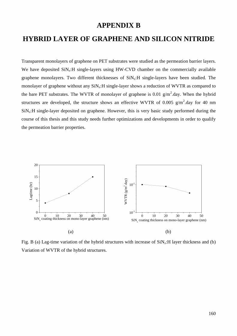
160
APPENDIX B
HYBRID LAYER OF GRAPHENE AND SILICON NITRIDE
Transparent monolayers of graphene on PET substrates were studied as the permeation barrier layers.
We have deposited SiNx:H single-layers using HW-CVD chamber on the commercially available
graphene monolayers. Two different thicknesses of SiNx:H single-layers have been studied. The
monolayer of graphene without any SiNx:H single-layer shows a reduction of WVTR as compared to
the bare PET substrates. The WVTR of monolayer of graphene is 0.01 g/m2.day. When the hybrid
structures are developed, the structure shows an effective WVTR of 0.005 g/m2.day for 40 nm
SiNx:H single-layer deposited on graphene. However, this is very basic study performed during the
course of this thesis and this study needs further optimizations and developments in order to qualify
the permeation barrier properties.
0 10 20 30 40 500
5
10
15
20
SiNx coating thickness on mono-layer graphene (nm)
Lag
tim
e (h
r)
0 10 20 30 40 5010
-3
10-2
WV
TR
(g
/m2.d
ay)
SiNx coating thickness on mono-layer graphene (nm)
(a) (b)
Fig. B (a) Lag-time variation of the hybrid structures with increase of SiNx:H layer thickness and (b)
Variation of WVTR of the hybrid structures.

161
LIST OF PUBLICATIONS
This thesis is based on following journal and conference contributions:
Publications in Journals:
[1] S. Majee, M.F. Cerqueira, D. Tondelier, B. Geffroy, Y. Bonnassieux, P. Alpuim, J.E. Bourée, “The
Effect of Argon Plasma Treatment on the Permeation Barrier Properties of Silicon Nitride Layers”,
Surface & Coatings Technology, 235 (2013) 361-366. [Featured article in Advances in
Engineering]
[2] S. Majee, M. F. Cerqueira, D. Tondelier, J. C. Vanel, B. Geffroy, Y. Bonnassieux, P. Alpuim, J. E.
Bourée, “Influence of Low Energy Ar Plasma Treatment on the Moisture Barrier Performance of Hot
Wire -CVD Grown SiNx Multilayers”, Japanese Journal of Applied Physics, 53 (2014) 05FM05.
[3] S. Majee, M. F. Cerqueira, D. Tondelier, J. C. Vanel, B. Geffroy, Y. Bonnassieux, P. Alpuim, J. E.
Bourée, “Permeation barrier performance of HW-CVD grown silicon nitride films treated by argon
plasma”, Special Issue of Thin Solid Films (accepted, under process).
Conferences contributions:
[1] S. Majee, M.F. Cerqueira, D. Tondelier, B. Geffroy, Y. Bonnassieux, P. Alpuim, J.E. Bourée,
“Encapsulation for organic devices deposited on polymer substrates”, IONS conference, February
2012, Paris.
[2] S. Majee, M.F. Cerqueira, D. Tondelier, B. Geffroy, Y. Bonnassieux, P. Alpuim, J.E. Bourée,
“Silicon nitride multilayers as permeation barrier for OLEDs. Effect of Argon plasma treatment”, E-
MRS Spring meeting, May 2012, Strasburg.
[3] S. Majee, M.F. Cerqueira, D. Tondelier, B. Geffroy, Y. Bonnassieux, P. Alpuim, J.E. Bourée, “Effect
of argon plasma surface treatment on the permeation barrier performance of silicon-nitride thin
films”, HWCVD7 conference, October 2012, Japan.
[4] S. Majee, M.F. Cerqueira, D. Tondelier, B. Geffroy, Y. Bonnassieux, P. Alpuim, J.E. Bourée,
“Multilayers of Silicon nitride thin films as an encapsulation barrier for flexible organic electronic
devices”, DIELOR conference, November 2012, Limoges, France.
162
[5] S. Majee, “Silicon Nitride multilayers as a permeation barrier for PET based organic devices”,
JAIST International School on Cat-CVD, March 2013, Japan.
[6] S. Majee, M.F. Cerqueira, D. Tondelier, B. Geffroy, Y. Bonnassieux, P. Alpuim, J.E. Bourée, “The
Effect of Argon Plasma Treatment on the Performance of Silicon Nitride Permeation Barrier
Multilayers for Organic Photovoltaics”, E-MRS Spring meeting, May 2013, Strasburg.
[7] S. Majee, M.F. Cerqueira, D. Tondelier, B. Geffroy, Y. Bonnassieux, P. Alpuim, J.E. Bourée, “Effect
of Argon Plasma Treatment on Silicon Nitride Barrier films for OPV cells”, MRS-JSAP Joint
Symposium, September 2013, Japan.
[8] S. Majee, M.F. Cerqueira, D. Tondelier, B. Geffroy, Y. Bonnassieux, P. Alpuim, J.E. Bourée,
“Permeation barrier performance of inorganic / organic / inorganic hybrid structure for organic
photovoltaic devices”, Matériaux et Nanostructures π-Conjugués (MNPC) conference, October 2013,
Annecy, France.
[9] S. Majee, M.F. Cerqueira, D. Tondelier, B. Geffroy, Y. Bonnassieux, P. Alpuim, J.E. Bourée, “Effect
of Low Energy Ar Plasma Treatment on the Morphology of Hot-Wire CVD Grown SiNx Interface and
on the Permeation Barrier of Stacked SiNx Single-layers”, JNPV2013 conference (French meeting on
photovoltaics), December 2013, Dourdan, France.
[10] S.Majee, “Encapsulation for flexible organic electronics: Protection from environment”,
International Displays Research Workshop 2014 (10th
French-Korean Joint Workshop), January 2014,
Palaiseau, France.

163
CURRICULUM VITAE
Subimal Majee
Date of birth: 01-03-1984
Citizen of: India
2010-2014: Doctoral studies at the Laboratoire de Physique des Interfaces et Couches Minces,
Ecole Polytechnique, CNRS (UMR 7647), Palaiseau, 91128, France
2009-2010: Master of Science (Material Science & Nano Objects) from Ecole Polytechnique,
France
2008-2010: Master of Technology (Radio Physics and Electronics) from University of Calcutta,
India
2005-2008: Bachelor of Technology (Radio Physics and Electronics) from University of Calcutta,
India
2002-2005: Bachelor of Science (Physics) from University of Calcutta, India
2000-2002: Higher Secondary (10+2) in Science, STP High (H.S.) School, West Bengal, India