development of a test-bed for smart antennas, using...
TRANSCRIPT

University of Twente
Faculty of Electrical Engineering
Chair Signals and Systems
Development of a test-bed for smart antennas, using digital beamforming
By
Taco Kluwer
M. Sc. Thesis
Report no: S&S-015.01
December 2000-August 2001
Supervisors: Prof. Dr. Ir. C.H. Slump
Ir. R. Schiphorst
Ir. F.W. Hoeksema


SUMMARY
This report describes the development of a smart antenna test-bed. The test-bed is configured as a receiver
and can process the signals of a maximum of four antennas. The receiver structure is based on the
heterodyne receiver concept. The heterodyne receiver is characterized by two stages. The first stage
converts the received signal to an intermediate frequency, and the second stage converts this signal to the
baseband.
A setup is configured to simulate the first stage by using programmable function generators. The second
stage of the front-end is performed digitally. For this a quad analog-to-digital converter is used in
combination with a digital signal processor. The analog-to-digital converter and the digital signal processor
are editions of Texas Instruments for evaluation purposes. The digital downconversion and the
beamforming tasks are defined by software.
Two algorithms are considered to be implemented; the Least Mean Square algorithm and the Constant
Modulus algorithm. The Constant Modulus Algorithm is simpler to implement as it is a blind algorithm and
it does not require synchronization.
The software platform is formed by a real-time operating system, which is called DSP/BIOS. The software
objects that are designed, function as real-time tasks. The test-bed is designed for continuous operation. A
driver for the analog-to-digital converter is implemented. The digital downconverter is implemented and
tested for two channels. Extension to four channels can be done easily.
The software-defined digital beamformer is implemented for 2 channels. The system has been tested for
MSK signals for the interfering signal as the desired signal. The system demonstrated successful
suppression of the interfering signal.

Preface
Wireless telecom has always been one of my major interests. Nowadays the telecom sector is growing fast
and its behavior is dynamic, hazardous and turbulent. At the start of a 3rd generation network for mobile
communications, new technologies, demands and restrictions arise. Technologies as GSM, DECT, IS95
will evolve to new standards such as UMTS. Besides these technologies Bluetooth, wireless LAN and
HomeRF came up, showing many completely new insights and applications. This enormous amount of
technology and its potential, ask for creative and smart solutions.
One of the developments in wireless telecom that interests me is the smart antenna. Smart antenna
technology can have great effect on many important parameters in the wireless communication. Benefits to
be gained are among others in the area of bandwidth, bit rates, interference rejection, power economy, and
reliability. High potential indeed, and therefore smart antenna technology is at this moment a hot topic for
the wireless industry. The basic idea behind smart antennas is that multiple antennas processed
simultaneously allow static or dynamical spatial processing with fixed antenna topology. The pattern of the
antenna in its totality is now depending partly on its geometry but even more on the processing of the
signals of the antennas individually. Smart antennas enable beamforming to aim at targets or pattern
modification to form the best solution for signal to noise performance or energy economy.
For my Master’s thesis I chose smart antennas as an area to focus on. I approached the chair Signals and
Systems for my thesis as its research interests share a common field with my interests. During my thesis an
assignment was formed and carried out. The final result of the thesis is this document containing my
experiences and achievements.
I would like to thank my supervisors, Kees Slump, Roel Schiphorst and Fokke Hoeksema, for their support
and advice during the Thesis. Furthermore I would like to thank Henny Kuipers and Geert-Jan Laanstra for
their support on the practical work.
Taco Kluwer

Table of Contents
1 Introduction .................................................................................................................1
1.1 Defining the assignment.............................................................................................. 2
1.2 Overview ..................................................................................................................... 2
2 Smart antennas fundamentals.....................................................................................5
2.1 Different approaches................................................................................................... 5
2.2 Smart antenna basics .................................................................................................. 7
2.3 Adaptive beamforming ............................................................................................... 9
2.4 The LMS algorithm .................................................................................................. 10
2.5 Constant Modulus Algorithm................................................................................... 13
3 Radio frequency front-end.........................................................................................15
3.1 Radio Frequency Transceiver .................................................................................. 15
3.2 Receiver Fundamentals............................................................................................. 17
3.3 Receiver building blocks ........................................................................................... 21
3.4 Receiver architectures in practice ............................................................................ 22
3.5 RF design proposal ................................................................................................... 25
4 Digital receiver fundamentals ...................................................................................29
4.1 Differential detection ................................................................................................ 30
4.2 Bit clock recovery...................................................................................................... 31
5 The test-bed: implementation ....................................................................................33

5.1 System overview........................................................................................................ 33
5.2 Hardware implementation........................................................................................ 34 5.2.1 Texas Instruments TMS320C6711 development board........................................................ 35
5.2.2 THS1206 AD converter evaluation module.......................................................................... 36
5.3 Hardware performance ............................................................................................ 37
5.4 Software implementation.......................................................................................... 39 5.4.1 DSP/BIOS............................................................................................................................. 39
5.4.2 Real-time analysis ................................................................................................................. 39
5.4.3 Real-time program structure ................................................................................................. 41
5.5 Software design ......................................................................................................... 42 5.5.2 Start AD conversion.............................................................................................................. 44
5.5.3 Process ping or pong............................................................................................................. 44
5.5.4 DDCping/pong...................................................................................................................... 45
5.5.5 Beamform ............................................................................................................................. 46
5.6 Software to be implemented ..................................................................................... 46
6 Test results..................................................................................................................47
6.1 Thread test results..................................................................................................... 47
6.2 Digital downconverter .............................................................................................. 51
6.3 Beamform algorithm................................................................................................. 52 6.3.1 Experiment 1......................................................................................................................... 53
6.3.2 Experiment 2......................................................................................................................... 56
7 Conclusions ................................................................................................................59
8 Recommendations......................................................................................................61
References.........................................................................................................................63
Appendix A, Experiences with TI tools ...........................................................................65
Appendix B, Matlab code .................................................................................................67
Appendix C, C source code ..............................................................................................75
Appendix D, Technology updates ....................................................................................89

1
1 Introduction
In wireless telecom there is the ever-lasting search to new technologies for improvement of bandwidth,
capacity, quality and so on. A lot of achievements have been made regarding modulation techniques and
coding to find reliable and more efficient ways to send information wireless. One of the technologies that
can contribute to the improvement of wireless systems is the smart antenna.
A smart antenna is a system in which the performance of the antenna pattern can be improved. This is done
by multiple antennas, which are processed simultaneously. Dynamic changing of the antenna pattern
enables the system to form a beam at a target, and with that improvement of its signal to noise ratio. The
beam can also be formed to remove interference from certain directions. Spatial separation of multiple
users by multiple beams enables more users per cell, as the users can re-use the frequency. These are a few
examples of the use of a smart antenna system for improvement of a wireless system.
In the past a lot of effort is made to gain insight in the working of smart antenna systems. Algorithms,
which enable beamforming or noise reduction have been simulated and compared with each other. Now a
demand arises to see how these systems work in practice. What is possible with these systems and how well
do the beamforming smart antennas perform in a real system? When using a real system, the components
are not ideal and in the system design trade-offs are made to find a good working system. It is not about
finding the ‘best’ system, but finding the best system under certain circumstances or constraints. A way to
reveal these design parameters and gain insight in the actual system can be done by implementing a test-
bed. The test-bed is a set up where the various algorithms can be tested in a real system. This thesis is
carried out to design a flexible test-bed for smart antennas, to actually test smart antenna algorithms in a
communication system, which explains the title of the Thesis:
“Development of a test-bed for smart antennas using digital beamforming”

2
1.1 Defining the assignment
To structure the work, the assignment has to be defined. A scope is first defined to form a framework to
work within. The scope of the thesis is formed by the demands for the test-bed:
1. The test-bed will be based on digital beamforming
2. The test-bed will involve a real-time system
3. The test-bed will enable algorithm testing and development
4. The test-bed will be closely related to software radio
5. The test-bed will be flexible
Digital beamforming indicates the use of a digital system performing the actual beamforming function of
the smart antenna test-bed by means of digital signal processing. The software radio concept is closely
related with this and states that digital algorithms will also perform certain transceiver functions. A
favorable choice is the use of digital signal processors. When designing a flexible system closely related to
software radio a real-time system is necessary. Flexibility is required to extend the system easily and to test
algorithms or transceiver functionality.
In the assignment the test-bed is considered to be a receiver. The test-bed’s functionality will be the
reception, downconversion and beamforming of the incoming signals. The assignment can be formulated as
followed:
“Develop a flexible smart antenna receiver that uses digital beamforming”
This definition can be split up into the following sub-definitions:
1. Research the practical issues concerned with smart antennas
2. Implement a smart antenna test-bed or setup within the framework defined above
3. Demonstrate the test-bed
Research of the practical issues is necessary, as the constraints for smart antenna receivers are different
from conventional single antenna systems. A working system has to be developed, conform the defined
scope. The complete setup will demonstrate a beamforming system using at least one beamforming
algorithm.
1.2 Overview Chapter 2 will discuss the fundamental aspects of the smart antenna. It includes the Least Mean Square
algorithm and the Constant Modulus algorithm, which are both simple beamforming algorithms.
In Chapter 3 the radio frequency transceiver aspects are discussed. The Chapter will start with the
theoretical evaluation of receiver architectures. After that the practice of implementing radio frequency
components is discussed.

3
The concept of a digital receiver is discussed in Chapter 4. This chapter will explain the working of a
digital downconverter. Besides the digital downconverter the demodulation for a (Gaussian) Minimum
Shift Keying receiver (MSK) can be found in this chapter.
In Chapter 5 the implementation of the test-bed is described. The setup consists of hardware and software
components, and development tools. The radio front-end’s behavior is simulated with programmable
function generators.
After that, the system is tested, and the results can be found in Chapter 6. The conclusion and
recommendations are given in Chapter 7 and Chapter 8.

4
5
2 Smart antennas fundamentals
This section treats the different aspects of smart antennas. A smart antenna usually involves spatial
processing and adaptive filtering techniques. The field of application is very large, ranging from signal to
noise improvement to the user capacity enlargement of the mobile network. A typical application will
involve an adaptive algorithm to create a beam to track a user or to eliminate noise sources and therefore
the smart antenna is also referred to as adaptive array or adaptive beamformer. This chapter discusses two
algorithms, the Least Mean Square algorithm and the Constant Modulus algorithm.
2.1 Different approaches
The first approaches to smart antennas or adaptive arrays were made for military purposes. The aim of
these investigations was the suppression of strong jamming signals in military communications. Later, the
mobile industry noticed adaptive arrays as a way to reuse frequency. Nowadays there are many applications
that could profit from adaptive array. Benefits can be split up in the following fields [1]:
1. Coverage; The antenna gain and the interference rejection can increase the cell coverage.
2. Capacity; Space division multiple access is a technique that enables a higher frequency reuse factor,
especially when combined with a dynamic channel assignment strategy.
1. Signal Quality; The use of beamforming will result in less co-channel interference, higher gain, and
with that, better signal to noise performance.
2. Access Technology; In addition to temporal multiple access techniques as FDMA, TDMA and CDMA,
adaptive beamforming gives new possibilities for user detection. Equalization is less complex as the
multi-path fading and delay spread is reduced.
3. Power Control; The demands for power control algorithms can be eased with the use of adaptive arrays
and the use of angular information about the users. The quality of UMTS for example, depends largely
on efficient power control with respect to the near-far problem and therefore it could benefit from
adaptive arrays.
4. Handover; The use of angular information, and as a result of this, a better estimation of the users
location can improve handover planning and execution.
5. Basestation Transmit Power; An adaptive array can transmit less power compared to the situation
where no adaptive antenna is used, while the power level at the portable terminal remains the same.
6
6. Portable Terminal Transmit Power; If the antenna gain of the receiving base station is improved in the
direction of the mobile, the transmit power of the mobile can be lowered, enabling more standby time
or processing power.
It is clear that by using the adaptive array, the overall performance can be improved, giving freedom to use
this improvement as a trade-off between the above-mentioned benefits. For mobile operators all of the
above mentioned benefits could result in cost reduction or quality improvement. It is up to the operator to
find out which benefits are important.
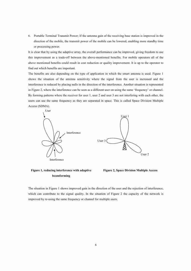
The benefits are also depending on the type of application in which the smart antenna is used. Figure 1
shows the situation of the antenna sensitivity where the signal from the user is increased and the
interference is reduced by placing nulls in the direction of the interference. Another situation is represented
in Figure 2, where the interference can be seen as a different user on using the same ‘frequency’ or channel.
By forming patterns where the receiver for user 1, user 2 and user 3 are not interfering with each other, the
users can use the same frequency as they are separated in space. This is called Space Division Multiple
Access (SDMA).
Figure 1, reducing interference with adaptive
beamforming
Figure 2, Space Division Multiple Access
The situation in Figure 1 shows improved gain in the direction of the user and the rejection of interference,
which can contribute to the signal quality. In the situation of Figure 2 the capacity of the network is
improved by re-using the same frequency or channel for multiple users.

7
2.2 Smart antenna basics
The smart antenna is basically a set of receiving antennas in a certain topology. The received signals are
multiplied with a factor, adjusting phase and amplitude. Summing up the weighted signals, results in the
output signal. The concept of a transmitting smart antenna is rather the same, by splitting up the signal
between multiple antennas and then multiplying these signals with a factor, which adjusts the phase and
amplitude. Figure 3 represents the concept of the smart antenna. The signals and weight factors are
complex.
Figure 3, smart antenna concept for a receiving antenna
A linear array is shown in Figure 4. In this figure, d is the distance between the antennas and θ is the angle
at which the wave front arrives.
Figure 4, linear array
The following mathematical foundations on the smart antenna concept can be found in [1]. If the wavefront
arrives at the array antenna as shown in Figure 4, the wavefront will be earlier on antenna element k+1 than
element k. The difference in length between the paths is dsinθ. If the arriving signal is a harmonic signal or
frequency, then the signal arriving at antenna k+1 is leading in phase compared with antenna k. The signal
that arrives at antenna element zero is considered to have a phase lead of zero. The signal that arrives at
antenna k, leads in phase with ξkdsinθ, where ξ=2π/λ and λ is the wavelength.

8
This leads to the so-called array propagation vector defined by:
sin ( 1) sin1Tj d j K de eξ θ ξ θ− = v L (2.1)
This vector contains the information of the arrival of the signal. K is the number of antenna elements used
in the array and k is the index for the antenna element. The weight vector is defined by:
[ ]0 1 1T
Kw w w−
=w L (2.2)
Now the array factor is defined by:
( )
( )
,( , )
,Ty
Fxξ θ
ξ θξ θ
= = w v (2.3)
The array factor is the response of the signal arriving from angle θ; y(ξ,θ) and x(ξ,θ) are respectively the
input and output of the beamforming array. If we consider ξ and d being fixed parameters of the antenna,
chosen for a given frequency, combining (2.3) with (2.1) and (2.2) gives:
( )1
sin
0
Kj kd
kk
F w e ξ θθ
−
=
=∑ (2.4)
The complex weight is defined by:
jkk kw A e α
= (2.5)
Combining the array factor from (2.4) with the complex weight from (2.5) gives:
( ) ( )1
sin
0
Kj kd k
kk
F A e ξ θ αθ
−
+
=
=∑ (2.6)
If a signal is arriving at the antenna array at an angle θ0, it is clear that the array response will be maximal
by adjusting the phase of the complex weight with:
0sindα ξ θ= − (2.7)
Figure 5 shows the effect of an array response of a linear array with 8 antennas with the beam steered to the
front at θ0 equal to zero and 45 degrees. The array response is generated by using MATLAB simulations.
There are many antenna topologies in which smart antennas can be configured, as circular array or planar
arrays. For these configurations array factors have been derived and can be found in [1]. The linear array is
used for this thesis, and therefore the derivations for different configurations are left out of consideration.

9
-80 -60 -40 -20 0 20 40 60 80-30
-25
-20
-15
-10
-5
0
5array amplitude response
(dB
)
angle(degrees)
0 degrees45 degrees
Figure 5, beam pattern with beam steered to 0 and 45 degrees
2.3 Adaptive beamforming Adaptive beamforming can be done in many ways. Many algorithms exist for many applications varying in
complexity. Most of the algorithms are concerned with the maximization of the signal to noise ratio. A
generic adaptive beamformer is shown in Figure 6. The weight vector w is calculated using the statistics of
signal x(t) arriving from the antenna array. An adaptive processor will minimize the error e between a
desired signal d(t) and the array output y(t).
Figure 6, adaptive beamforming configuration
One of the simplest algorithms for adaptive processing is based on the Least Mean Square (LMS) error.
Although the complexity of the algorithm is very low, its results are satisfying in many cases. The
algorithm is very stable and it needs few computations, which is important for system implementation. The
computational power of many systems is limited and should be managed wisely.
10
The algorithm is based on knowledge of the arriving signal. The knowledge of the received signal
eliminates the need for beamforming, but the reference can also be a vector that is partly known, or
correlated with the received signal. For example, the training sequence in the GSM standard, intended for
channel equalization, could be used for beamforming. The rest of the signal is unknown, and beamforming
using LMS can only be performed on the known training sequence.
When the adaptive algorithm is not using this knowledge, but statistic information of the signal, it is called
blind beamforming. There are several algorithms for blind beamforming. For example the Constant
Modulus algorithm (CMA) uses the knowledge that the modulus of the signal is constant. There are many
modulation schemes where the modulus is kept constant. CMA is one of the most simple blind
beamforming algorithms.
2.4 The LMS algorithm
The LMS algorithm can be considered to be the most common adaptive algorithm for continues adaptation.
It uses the steepest-descent method and recursively computes and updates the weight vector. Due to the
steepest-descend the updated vector will propagate to the vector which causes the least mean square error
(MSE) between the beamformer output and the reference signal. The following derivation for the LMS
algorithm is found in [1]. The MSE is defined by:
( ) ( ) ( )22 Ht d t tε
∗ = − w x (2.8)
d(t)* is the complex conjugate of the desired signal. The signal x(t) is the received signal from the antenna
elements, and wHx(t) is the output of the beamform antenna and (.)H is the Hermetian operator. The
expected value of both sides leads to:
( ){ } ( ){ }2 2 2 H HE t E d tε = − +w r w Rw (2.9)
In this relation the r and R are defined by:
( ) ( ){ }E d t t∗
=r x (2.10)
( ) ( ){ }HE t t=R x x (2.11)
R is referred to as the covariance matrix. If the gradient of the weight vector w is zero, the MSE is at its
minimum. This leads to:
( ){ }( )2 2 2 0E tε∇ = − + =w r Rw (2.12)
The solution of (2.12) is called the Wiener-Hopf equation for the optimum Wiener solution:
1opt
−
=w R r (2.13)

11
The LMS algorithm converges to this optimum Wiener solution. The basic iteration is based on the
following simple recursive relation:
( ) ( ) { }( )( )2112
n n Eµ ε+ = + −∇w w (2.14)
And combining (2.14) with (2.12) gives:
( ) ( ) ( )( )1n n nµ+ = + −w w r Rw (2.15)
The measurement of the gradient vector is not possible, and therefore the instantaneous estimate is used
defined by (2.16) and (2.17).
( ) ( ) ( )ˆ Hn n n=R x x (2.16)
( ) ( ) ( )ˆ n d n n∗
=r x (2.17)
By rewriting (2.15) using the instantaneous estimates, the LMS algorithm can be written in its final form
(2.18).
( ) ( ) ( ) ( ) ( ) ( )( )
( ) ( ) ( )
ˆ ˆ ˆ1
ˆ
Hn n n d n n n
n n n
µ
µ ε
∗
∗
+ = + −
= +
w w x x w
w x (2.18)
One of the issues on the use of the instantaneous error is concerned with the gradient vector, which is not
the true error gradient. The gradient is stochastic and therefore the estimated vector will never be the
optimum solution. The steady state solution is noisy; it will fluctuate around the optimum solution. By
decreasing µ the precision will improve but it will decrease the adaptation rate. An adaptive µ could solve
this issue by starting with a large µ and decrease the factor when the vector converges.
An adaptive array is simulated in MATLAB by using the LMS algorithm. When an array of 4 antennas is
used, there is a maximum of 3 nulls that can eliminate the interferer. Figure 7 shows the convergence of the
array for 2 interferers. The minimum error is a result of the extra ‘system’ noise that is added to all
antennas. The interference signals are Gaussian white noise, zero mean with a sigma of 1. The extra system
noise to all antennas is white noise with zero mean and a sigma of 0.1. The received signals are MSK
signals with an oversampling of 4 and have an amplitude of 1 in the simulations.
The true array output y(t) is converging to the desired signal d(t). After 40 samples the signal is at its
minimum due to the system noise. The LMS cannot filter the system noise, as it is not correlated for all
four antennas. The resulting array vector has an amplitude response as shown in Figure 8.
The interferers are cancelled by placing nulls in the direction of the interferers. The received signal arrives
at an angle of 25 degrees and the array response is 0 dB. The LMS algorithm clearly works sufficient as the
strong interferers are reduced. The source code for the MATLAB simulations can be found in Appendix B.

12
0 50 100 150 200 250-15
-10
-5
0
5ph
ase(
rad)
desired signal 25 degrees interferers 0 and -40 degrees
phase(d)phase(y)
0 50 100 150 200 2500
2
4
6
8
ampl
itude
|d||y|
0 20 40 60 80 100 120 140 160 180 2000
0.5
1
ampl
itude
sample(index)
|error|
Figure 7, LMS algorithm for an adaptive array with 4 antennas and 2 interferers.
-80 -60 -40 -20 0 20 40 60 80-30
-25
-20
-15
-10
-5
0
5
10amplitude response antenne pattern
(dB
)
angle(degrees)
Figure 8, amplitude response after beamforming

13
2.5 Constant Modulus Algorithm
The CM algorithm is used for blind equalization of signals that have a constant modulus. The MSK signal,
for example, is a signal that has the property of a constant modulus. The algorithm that updates the weight
coefficients is exactly the same as for the LMS algorithm (2.18). The error is different and defined by [1]:
( ) ( )( ) ( )2
1n y n y nε∗
= − (2.19)
which is known as Godard’s algorithm. The CM algorithm can be found in many derived forms. The error
function for a derived version is given by [19] and [20]:
( )( )
( )( )
y nn y n
y nε = − (2.20)
This error can be compared with (2.18), as the first term of (2.20) can be seen as a desired signal d(n) in
(2.18). This algorithm is simulated by MATLAB and the result of the experiments can be found in Figure
9. The algorithm converges slower than the LMS algorithm. The simulation was done with a relatively low
system noise, which is Gaussian noise with a sigma of 0.01. The interferers are the same as in the LMS
experiment only the angle of arrival of the signals is different. The signals of the interferers arrive at an
angle of –10 and –40 degrees. The signal to be received arrives at an angle of 10 degrees. Figure 10 shows
the amplitude response of the adaptive array, where both interferers are rejected. The results demonstrate
the concept of the CM algorithm, but more experiments are necessary to understand its properties. During
the efforts to simulate the CM algorithm it was clear that the algorithm is less stable than the LMS
algorithm. Simulations of the algorithm using the error defined in (2.19) have not resulted in stable results.
In the simulations there was no synchronization necessary. In a real system, the LMS algorithm requires
that the reference vector d(n) is synchronized with the array output y(n). The advantage of the CM
algorithm is the fact that it only needs the instantaneous amplitude of the array output |y(n)| and therefore
no synchronization is required. Due to this property, the CM algorithm is relative simple to implement.
Synchronization of the LMS algorithm usually involves the use of correlators in the digital beamformer to
align the desired vector with the incoming signal. The source code of the MATLAB experiments can be
found in Appendix B.

14
0 50 100 150 200 250-15
-10
-5
0
5ph
ase(
rad)
desired signal 10 degrees interferers -10 and -40 degrees
phase(d)phase(y)
0 50 100 150 200 2500.5
1
1.5
2
ampl
itude
|d||y|
0 20 40 60 80 100 120 140 160 180 2000
0.5
1
ampl
itude
sample(index)
|error|
Figure 9, CM algorithm for an adaptive array with 4 antennas and 2 interferers
-80 -60 -40 -20 0 20 40 60 80-30
-25
-20
-15
-10
-5
0
5
10amplitude response antenne, desired signal: 10 degrees, interferers: -10 and -40 degrees
(dB
)
angle(degrees)
Figure 10, amplitude response after beamforming

15
3 Radio frequency front-end
As there are many approaches to smart antenna implementations, it is necessary to analyze the possibilities
before actually building the system. This chapter will discuss the RF front-end. In the first part the different
architectures are considered. For an adaptive array there are certain aspects that need to be covered by the
architecture. In general for every antenna in the array an RF front-end is necessary, performing up and
downconversion and filtering. At high frequencies measurements are more subjected to feedback, noise and
distortion. The length of the cables, the shape of connectors and the PCB layout are all contributing to the
quality of the transceiver. Therefore the RF area can be considered a special field of work, and if it is part
of a thesis a high level of expertise is required to develop a system. A way to avoid difficulties in this area
would be the use of common of the shelf (COTS) transceivers. An implementation of a front-end receiver
from COTS RF components appeared to be impossible, as most of the COTS components are designed for
specific operation in existing communication standards or they are expensive professional products.
Another way to avoid part of the design in the RF area, is to use evaluation modules from existing RF
integrated circuits. The evaluation boards contain a setup with extra components and PCB board, to
evaluate the product easily. The evaluation boards can also function as a reference design, for an eventual
custom design.
The chapter includes a general overview of RF aspects. The chapter considers the different architectures
and an evaluation is given supported by practical as well as mathematical foundations. Furthermore a
proposal is made for an RF front-end for a receiver with simple components. This proposal can be used in
the future as a reference for the actual design and implementation. Due to the lack of expertise in the RF
field it was not possible to develop a suitable front-end.
3.1 Radio Frequency Transceiver
The RF part of a wireless communication system generally provides a conversion between the radio or
microwave frequency and baseband or intermediate frequencies (IF). This is called up and
downconversion, which is respectively related to up and down shifting in the frequency spectrum of the
signal that needs to be received or transmitted. In the past years the RF technology has improved a lot, due
to the growth of the wireless industry. Many chip manufacturers develop integrated circuits for RF
applications covering all analog and digital communication standards in the world. These products range
16
from fully integrated circuits for digital standards, to flexible building blocks for custom RF products. RF
designing is now a special field of expertise, where a practical approach is the common way to work. It is
leaded by the mobile industry and the ICs are more and more fully integrated, providing a complete
receiver, transmitter or transceiver to be implemented in a mobile communication device. The mobile
communication standards DECT, GSM, IS-95, D-APMS, are just a few from the pile of mobile
communication technologies that exist all over the world.
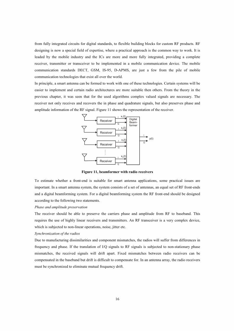
In principle, a smart antenna can be formed to work with one of these technologies. Certain systems will be
easier to implement and certain radio architectures are more suitable then others. From the theory in the
previous chapter, it was seen that for the used algorithms complex valued signals are necessary. The
receiver not only receives and recovers the in phase and quadrature signals, but also preserves phase and
amplitude information of the RF signal. Figure 11 shows the representation of the receiver.
Figure 11, beamformer with radio receivers
To estimate whether a front-end is suitable for smart antenna applications, some practical issues are
important. In a smart antenna system, the system consists of a set of antennas, an equal set of RF front-ends
and a digital beamforming system. For a digital beamforming system the RF front-end should be designed
according to the following two statements.
Phase and amplitude preservation
The receiver should be able to preserve the carriers phase and amplitude from RF to baseband. This
requires the use of highly linear receivers and transmitters. An RF transceiver is a very complex device,
which is subjected to non-linear operations, noise, jitter etc.
Synchronization of the radios
Due to manufacturing dissimilarities and component mismatches, the radios will suffer from differences in
frequency and phase. If the translation of I/Q signals to RF signals is subjected to non-stationary phase
mismatches, the received signals will drift apart. Fixed mismatches between radio receivers can be
compensated in the baseband but drift is difficult to compensate for. In an antenna array, the radio receivers
must be synchronized to eliminate mutual frequency drift.

17
3.2 Receiver Fundamentals
One of the most common building blocks of a receiver is the so-called mixer. The mixer can be seen as a
multiplier, which has two inputs, and one output. Generally the two inputs of the mixer are the received
signal and a locally generated signal called Local Oscillator (LO). The basic function of a mixer is a
translation of an input signal to a different frequency. The basic math that describes this function is formed
by the trigonometric relations:
( ) ( ) ( )( ) ( )( )1 2 1 2 1 21cos cos cos cos2
t t t tω φ ω ω ω φ ω ω φ + = − + + + + (3.1)
( ) ( ) ( )( ) ( )( )1 2 1 2 1 21cos sin sin sin2
t t t tω φ ω ω ω φ ω ω φ + = − + + + + (3.2)
The angular frequencies are represented by ω1 and ω2 and the phase difference by ϕ. The function of the
mixer is the translation of both frequencies to sum and difference frequencies. In receiver or transmitter
architectures, only one of the two output frequencies is interesting, and therefore the mixer will be
combined with an output filter, filtering either the sum or difference frequency.
To explain the basics of the receiver, an architecture is introduced, which is mathematically the simplest
form of a receiver, known as the direct-conversion receiver. The concept of the direct-conversion receiver
is visible in Figure 12.
Amplifier RF BPF LO
LPF
LPF
I
Q
Figure 12, Direct-conversion receiver
The receiver consists of an antenna, a low noise amplifier, a mixer stage and a low pass filter. The received
signal at the antenna is amplified and then injected to the mixer stage. The mixer stage usually consists of
two mixers, which demodulates the received signal. The oscillator, which provides a frequency, exactly the
same as the carrier is know as a Local Oscillator (LO). The LO is offered to both mixers with a 90 degree
phase shift for the demodulation of the in phase and quadrature component.
18
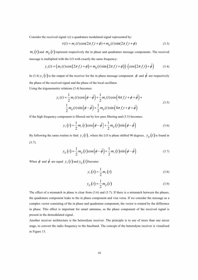
Consider the received signal r(t) a quadrature modulated signal represented by:
( ) ( ) cos(2 ) ( )sin(2 )I c Q cr t m t f t m t f tπ φ π φ= + + + (3.3)
( )Im t and ( )Qm t represent respectively the in phase and quadrature message components. The received
message is multiplied with the LO with exactly the same frequency:
( ) ( )( ) ( )( )ˆ( ) ( ) cos 2 ( )sin 2 cos 2I I c Q c cy t m t f t m t f t f tπ φ π φ π φ= + + + ⋅ + (3.4)
In (3.4) ( )Iy t is the output of the receiver for the in phase message component. φ and φ̂ are respectively
the phase of the received signal and the phase of the local oscillator.
Using the trigonometric relations (3.4) becomes:
( ) ( )
( ) ( )
1 1ˆ ˆ( ) ( ) cos ( )cos 42 2
1 1ˆ ˆ( )sin ( )sin 42 2
I I I c
Q Q c
y t m t m t f t
m t m t f t
φ φ π φ φ
φ φ π φ φ
= − + + + +
− + + +
(3.5)
If the high frequency component is filtered out by low pass filtering and (3.5) becomes:
( ) ( ) ( ) ( ) ( )1 1ˆ ˆcos sin2 2I I Qy t m t m tφ φ φ φ= − + − (3.6)
By following the same routine to find ( )Iy t , where the LO is phase shifted 90 degrees, ( )Qy t is found in
(3.7).
( ) ( ) ( ) ( ) ( )1 1ˆ ˆcos sin2 2Q Q Iy t m t m tφ φ φ φ= − + − (3.7)
When φ and φ̂ are equal ( )Iy t and ( )Qy t become:
( ) ( )12I Iy t m t= (3.8)
( ) ( )12Q Qy t m t= (3.9)
The effect of a mismatch in phase is clear from (3.6) and (3.7). If there is a mismatch between the phases,
the quadrature component leaks to the in phase component and visa versa. If we consider the message as a
complex vector consisting of the in phase and quadrature component, the vector is rotated by the difference
in phase. This effect is important for smart antennas, as the phase component of the received signal is
present in the demodulated signal.
Another receiver architecture is the heterodyne receiver. The principle is to use of more than one mixer
stage, to convert the radio frequency to the baseband. The concept of the heterodyne receiver is visualized
in Figure 13.
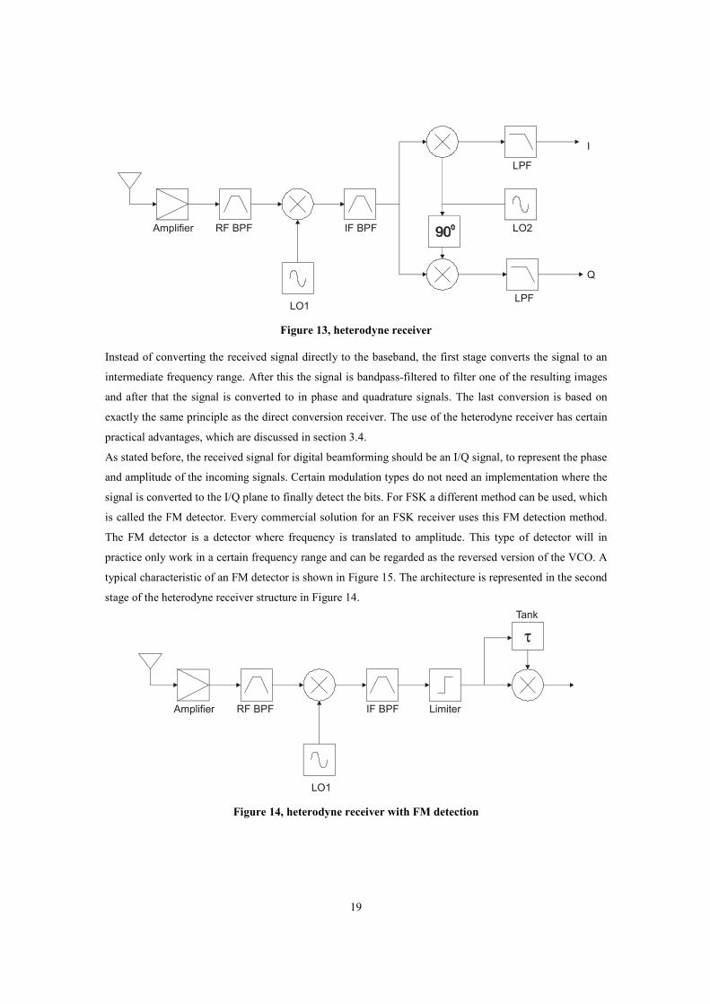
19
Amplifier RF BPF LO2
LPF
LPF
I
Q
LO1
IF BPF
Figure 13, heterodyne receiver
Instead of converting the received signal directly to the baseband, the first stage converts the signal to an
intermediate frequency range. After this the signal is bandpass-filtered to filter one of the resulting images
and after that the signal is converted to in phase and quadrature signals. The last conversion is based on
exactly the same principle as the direct conversion receiver. The use of the heterodyne receiver has certain
practical advantages, which are discussed in section 3.4.
As stated before, the received signal for digital beamforming should be an I/Q signal, to represent the phase
and amplitude of the incoming signals. Certain modulation types do not need an implementation where the
signal is converted to the I/Q plane to finally detect the bits. For FSK a different method can be used, which
is called the FM detector. Every commercial solution for an FSK receiver uses this FM detection method.
The FM detector is a detector where frequency is translated to amplitude. This type of detector will in
practice only work in a certain frequency range and can be regarded as the reversed version of the VCO. A
typical characteristic of an FM detector is shown in Figure 15. The architecture is represented in the second
stage of the heterodyne receiver structure in Figure 14.
Amplifier RF BPF
LO1
IF BPF
τ
Limiter
Tank
Figure 14, heterodyne receiver with FM detection

20
fc
f1
f2
frequency
output
Figure 15, FM detector characteristics: input frequency vs. output amplitude
The first mixer stage remains the same as the previous heterodyne receiver, the second stage however is not
using the in phase and quadrature detection but the FM detection method. The signal from the mixer is
limited and after that, multiplied with a phase-shifted version of itself. The phase shift is done by an
external network, which provides a phase shift depending on the frequency of the signal. After multiplying
the signal, the result is filtered by a low pass network. If the incoming signal is represented by:
( ) ( )( )cos 2r t f t tπ φ= + (3.10)
In (3.10) f(t) indicates the frequency modulation, where the frequency of the signal changes in time. The
actual message, which is the source for the frequency modulation is left out of the formula for simplicity.
( ) ( ) ( )( )cos 2r t f t t fτ
π φ θ= + + (3.11)
The phase shift by the external network is frequency depending, which explains the phase shift θ(f). Both
(3.10) and (3.11)will be multiplied in the mixer:
( ) ( ) ( )( ) ( ) ( )( )
( )( ) ( ) ( )( )
cos 2 cos 2
cos cos 4 ) 2
r t r t f t t f t t f
f f t t fτ
π φ π φ θ
θ π φ θ
= + + +
= + + +
(3.12)
A low pass network removes the high frequency component, which is the second term in the result of
(3.12). The resulting term is depending only on frequency of the input signal. The phase delaying network
will have a phase shift of 45 degrees for the carrier and zero and 90 degrees for the two frequencies on
which the signal is modulated. An important aspect is that the initial phase ϕ of the input signal is removed.
The result is only depending on the received frequency. The effect of the limiter on the system is that the
first term in the result of (3.12) is not a cosine but a linear function. As stated in the first part of the chapter,
phase preservation is necessary for a beamforming antenna array and therefore the FM detector is not
suitable for a beamforming antenna.

21
3.3 Receiver building blocks
The amount of different RF hardware products is very large. Often, these RF products are integrated
circuits. To understand the receiver it is important to understand the separate parts of the receiver. The
receiver can be split up in the following building blocks [8].
Antenna
The antenna is the interface between the receiver and the free air. The antenna has many characteristics as
gain, bandwidth, radiation efficiency, beam width, and beam efficiency. The antenna is the interface
between air and receiver and therefore the signals must be transferred as good as possible. The antenna
should be impedance matched between the free air and the receiver input.
Low-noise amplifier
The low-noise amplifier (LNA) is the first amplifier in the receiver chain. Its influence on the noise figure
is strong compared to the subsequent amplifiers. The amplifier must have a high gain and a very low noise
figure. Too much gain compresses amplifiers in the rest of the circuit. A tradeoff must be made between
gain and noise figure.
RF filters
The RF filter is necessary to filter the desired signal from out-of-band noise. Especially the so-called image
frequency, which has the same frequency difference to the LO as the desired signal, can distort the signal.
This way only the desired signal is transferred to the IF frequency.
Mixer
The mixer is a circuit, which is injected with the received signal and a reference signal from an oscillator.
The mixer converts the desired frequencies to the IF band. This requires the need for an RF filter as stated
before. A special type of mixer is the image reject mixer, which eliminates the image band in the mixer
itself. This type of mixer is not discussed in this thesis.
Local Oscillator
An oscillator generates the reference signal for the mixer. The oscillator consists of a phased lock loop and
a fixed reference oscillator. The fixed oscillator can be a digital circuit or a crystal oscillator. The phase
locked loop will lock to a divided version of the reference oscillator. By using a low pass filter in the phase
locked loop, phase noise is filtered out to get a steady oscillator. This loop filter slows down the lock-time
of the loop to the divided reference oscillator. This means that the loop filter should be narrow enough to
limit oscillator spurs, but wide enough to have a fast lock time.
22
IF filter
Only the IF frequency range is passed by the IF filter. The summed result of the LO and the carrier
frequency is removed as well as out of band noise.
Detector
The final stage is a detector to convert the signal to a suitable baseband signal. The type of detector is
depending on the modulation technique used. For FSK an FM detector is used, which converts the
frequency shifted signal to an analog NRZ signal. The I/Q demodulator is necessary if a form of quadrature
modulation is used.
3.4 Receiver architectures in practice
The direct-conversion receiver structure is simple in theory but difficult to realize in practice. Certain
problems make the realization of this structure nearly impossible [14]. The first problem is the leakage
from the local oscillator to the antenna port. As the LO has exactly the same frequency as the carrier signal,
this received signal is indistinguishable from the transmitted signal from other systems in the vicinity. At
higher frequencies, more problems arise, due to the effect of devices and circuits which act as antennas.
Very small interconnects can become an antenna in the gigahertz frequency range.
The second problem is the leakage from the RF port to the LO’s VCO. This effect only occurs at strong
signals, which can pull of the VCO’s frequency. Small phase shifts will induce the shifting of the VCO’s
frequency, with strong effects on phase-modulated systems. Therefore the problem is less present then the
leakage from the oscillator to the RF port, but still degrading the performance of the receiver.
The heterodyne receiver concept is not suffering from the above problems as the LO is not the same as the
carrier. The heterodyne receiver is widely used in al types of receivers from mobile terminals to FM radio
receivers. The heterodyne receiver has improved a lot in the last years because of new technologies. RLC
filters, ceramics, quartz crystals and surface acoustic wave devices have resulted in a high quality receiver
structure. However, due to these costly extra devices in the heterodyne receiver, the direct conversion
receiver is gaining popularity again and special on-chip architectures compensate for the previous described
problems.
The integrated circuits available are a combination of different types of building blocks to get the best
receiver performance. Different architectures exist, resembling one of the discussed receiver structures.
Many approaches are taken to design an architecture conform its design parameters. The common design
parameters for a receiver vary from low cost to low power, complexity, noise performance, gain and so on.
There is one aspect however that is similar for all integrated receivers. Filters are difficult to realize on a
chip. The consequence is that the signals leave the chip to be filtered and will return to the chip afterwards.
This is one of the most difficult aspects of designing an RF receiver. When the high frequency signals leave
the chip, the distances over which they travel are larger then on-chip. Small I/O pins on the chip and the

23
PCB lines suddenly become small antennas that pick up noise and introduce distortion and feedback.
Although the current SMD components are very small they are large enough to be sensitive to these effects.
The filters generally consist of the following types:
- Surface Acoustic Wave filter (SAW)
- RLC filter
- RC filter
The SAW filter is one of the most common RF filter nowadays and it is actually one component. The
advantage is that they are available in a wide range of frequencies or bandwidths. They are characterized by
a sharp cut-off, hence being very frequency selective. The disadvantage is that they are ceramic and
therefore very expensive. Furthermore SAW filters suffer from high insertion losses. Besides RF filters the
SAW filter is also used as IF filter when the frequency is relatively high. The output of a local oscillator
can be filtered also to eliminate noise.
The RLC filters are common types for IF filters and consist of a resistance, inductance and capacitance.
They can be formed in many ways and different orders. RLC filters involve multiple components and they
are therefore subjected to noise and feedback. If the IF frequency is low, even a low-pass RC filter can be
used. Low pass filters are also common to filter outputs of the detector.
The implementations of different systems range from application-specific single-chip solutions, to custom
configured solutions with multiple chips. Figure 16 shows a multi-chip transceiver configuration for a dual
band phone.
Figure 16, multi-chip design example for a dual band phone [22]

24
The example combines three chips to for a dual band phone for CDMA and AMPS. Both are using the
same IF frequency reducing the need for different designed filters and different local oscillators.
Furthermore it is clear that the system uses two stages for the up and down conversion and the baseband
signals are I/Q signals. The implementation requires a lot of hardware outside the chip, which should be
designed carefully. The RF hardware from chip to antenna and the high frequency filters, combined with
the PCB layout are most critical.
Figure 17, single-chip DECT transceiver design example [21]
Figure 17 shows a DECT transceiver implementation with only one chip. For the downconversion two
stages are used. The first filter is a bandpass filter for image rejection, the second is a SAW filter for IF
filtering and the third is an LC filter for the IF signals. The system uses an FM detector which needs
another off-chip filter, known as an RLC tank. The RLC tank is a network that provides the frequency
depending phase shift, for the FM detector. Details on the FM detector can be found in section 3.2 For the
upconversion a VCO is used with a PLL. The upconversion in DECT is less critical as it is a special form
of FSK, and can therefor be done with one stage in the form of a VCO.
Both the single and multi-chip transceiver systems show the diversity of hardware, which can be used to
implement receiver and transmitter functionality. When custom designs are necessary, multi-chip is a
solution, when a standard communication system is needed most of the dedicated single chips will satisfy.
Several types of systems allocate the frequency spectrum. Certain systems are being used quite extensively
like GSM, and others are protected, as they are part of critical systems for military purposes or the police.
This leaves little room for wireless radio experiments. The most interesting bands for experimenting with
RF equipment, without the need for a special shielded chamber, are summarized in Table 1.

25
System Frequency description
DECT 1.800-1.900
(GHz)
DECT is a standard for personal cellular systems. The
DECT system is for indoor telephone and data systems.
ISM 2.400-2.483
(GHz)
The ISM (Industrial, Scientific, Medical) band for indoor
applications. The transmit power is limited. The band will
be occupied with hiperlan and bluetooth devices
ISM 868 (MHz) Another ISM band
Table 1 , bands suitable for experiments
It should be able to do experiments in the DECT band without disturbing too much other DECT systems.
The range of a DECT system is limited and the number of channels is quite high. When there is not a data
DECT system in the area, which can use multiple systems, but only phone systems, the chance is limited
that the disturbance of one channel would be a problem.
The 2.4GHz ISM band is one of the most interesting bands, as the ISM band is totally free to use. The wide
bandwidth is interesting as well, it give a lot of space for the hardware to operate in.
The lower ISM is another option. Though quite narrow, the frequency is low, easing the constraint for the
hardware. However a larger wavelength will require larger antennas and a larger array, which can be a
disadvantage.
3.5 RF design proposal Due to the lack of experience in the field of RF design, the actual implementation of an RF frontend was
not possible in this thesis. An effort has been made to design the RF front-end for a beamforming system
and the result is a general RF design proposal. The design can be regarded as a high level reference design,
which fulfills the demands for a beamforming network. Before starting with the design, the following
guidelines are followed to form the design proposal:
The building blocks will be non-single chip solutions
It is necessary to be able to build a custom and flexible design. The single chip solutions are not suited for a
beamforming system. Most of the single chip solutions are designed for a non-suitable frequency range e.g.
GSM or D-AMPS etc. The single chip solutions in a suitable frequency range (for DECT or upbanded
DECT) are using an FM detector as described earlier in this chapter. This type of solutions is not suitable
for a digital beamforming system.

26
The building blocks are available in the form of evaluation modules
To be partly depending on the actual implementation issues concerned with RF design a evaluation module
is a good starting point for understanding and experimenting with the RF hardware. Most of the evaluation
modules are properly designed PCB’s with impedance matched inputs and outputs. A disadvantage could
be the fact that the combining of multiple evaluation modules involves signals traveling over long distances
when the evaluation modules are connected to each other.
The receiver will be able to preserve phase and amplitude information
This was also stated in the beginning of this chapter. The downconversion method must be able to preserve
the phase and amplitude of the signal. Most of the time the so-called mixers are sufficient for this function.
The receiver elements can be synchronized
To be sure that the total receiver is not suffering from independent phase drift for the different radios, it is
important that the receiver modules or building blocks can be synchronized in a way. This normally
involves synchronization of the LOs, or the use of one LO for different radio-chips.
IF sampling is used, which eliminates the use of a frequency detector
IF sampling involves the conversion of IF frequencies to the digital domain. This means that the second
analog stage in a receiver is not required anymore, which eliminates the use of analogue filters and another
local oscillator. The usage of IF sampling involves fast AD converters which can sample the rather high IF
frequencies. As the current AD converters are very fast ranging up to one gigasamples per second, the IF
frequency is not so much of a problem. The digital hardware following the AD converters to perform
downconversion and demodulation could be a problem, as the total throughput is subjected to the
processors limited memory bandwidth and processing power. In that case, additional hardware is necessary
to fulfill digital downconversion using for example an FPGA or ASIC digital downconverter.
Figure 18 shows the design concept following the earlier mentioned guidelines. The design uses a MAXIM
IC, which contains an LNA and a mixer per chip. The LO signal may be generated with a VCO module
which are also available from MAXIM. The LO needs to be divided 4 inputs. This involves power-splitting
to be sure that all impedances are matched. For filtering a Surface Acoustic Wave device (SAW) could be
used. These types of filters are known for its narrow filter characteristics. For IF frequencies with lower
constraints a RLC bandpass filter can be used or just a lowpass filter to remove the high frequency
component. After that the signals are filtered. Impedance matching is less problematic at IF frequencies.

27
Figure 18, design concept with MAX2411A
If enough RF expertise is available a custom PCB could be designed containing an appropriate number of
RF downconverters combined with micro-strips for powersplitting and impedance matching. The full
specification on the MAX2411A are available in [31]. The actual implementation of the design concept can
be found in Chapter 5. In the implementation programmable function generators replace the RF hardware.

28

29
4 Digital receiver fundamentals
This chapter will describe the properties of a digital receiver. The digital receiver is part of the test-bed in
the form of a digital downconverter. The sampled input signal is downconverted digitally to an in phase
and quadrature stream. The type of modulation that is selected is minimum shift keying (MSK) or if desired
Gaussian minimum shift keying (GMSK). Furthermore the signal needs to be demodulated. The signal is
converted from the I/Q signals to an actual bit sequence.
Instead of performing the conversion from radio frequency to the baseband using analogue integrated
circuits, it is possible to do the conversion partly analogue and partly digital. The current state-of-the-art
digital hardware is able to process digital signals up to one gigahertz. For certain receivers an all-digital
approach is possible. In that case, the antenna output is amplified, and sampled by a high speed AD
converter. Digital algorithms perform the complete transformation from the RF domain to the baseband.
When the digital hardware is less powerful, the RF frequency might be too high to be sampled and
processed. It is possible to sample the analogue signals after downconversion to the IF. The translation of
the IF domain to the baseband can than be done in digital hardware. This is called IF sampling, also know
as a form of direct sampling. The digital downconversion can be done by configurable hardware or by
software on a general-purpose processor. This functional unit, which performs the downconversion, is
called a digital downconverter (DDC). For digital communications, the generalized digital receiver is
comparable to the analogue version. Instead of using an analogue multiplier and a local oscillator, the
software or digital hardware fulfils these functions.
shows the generalized digital receiver. If the resulting I/Q signals are oversampled with a large factor, the
I/Q should be converted to a lower sample rate, which is called sample rate conversion.

30
Figure 19, generalized digital receiver
When the IF frequency is one fourth of the sample frequency, both the digital oscillators are reduced to a
repeating vector of [1 0 –1 0] for the ‘cosine’ oscillator and [0 1 0 –1] for the ‘sine’ oscillator. The digital
multiplier can perform multiplication at an even lower rate, as half of the numbers to multiply with is zero.
This is interesting as it reduces the load on the processor, or it simplifies the architecture for a digital
downconverter. A FIR filter is sufficient to filter the output of the multipliers to remove the summed
component. The result is that the input signal is converted to a baseband signal.
4.1 Differential detection To implement an MSK receiver on a DSP, several functional blocks are necessary. If the I and Q signals
are available, the receiver can be build using a differential detector, a frequency compensation loop, and a
bit clock recovery loop, followed by hard decision as represented in Figure 20.
Figure 20, digital receiver with frequency compensation and bit-clock recovery
The differential detector is a simple one bit differential detector, which compares the quadrature component
with the in-phase component and visa versa. The choice for a differential detector is following from the fact
that MSK modulation involves the phase shift of ½π or -½π . The differential detector is described by [17]:
( )n n n Ns z z∗
−= ℑ ⋅ (4.1)
sn is the output of the differential detector, zn is the nth sample representing the complex input vector. zn-N
is the complex input vector of one bit period back. N is the number of samples per bit. ( )ℑ ⋅ is the
imaginary part.
31
The value of N is Tb/Ts, where Tb is the bit period and Ts is the sampling period. Value N is an integer, but
normally the actual transmitter and receiver clocks are never exactly synchronized. The receiver might have
a sampling clock that is a little bit off. In this case, the digital downconverter will have a frequency offset
too as its frequency is coupled to the sampling frequency. A large frequency mismatch will cause the
signals to drift in the I/Q plane. This drift can be corrected by a digital frequency compensation loop. An
interesting approach is made in [17]. Frequency recovery is necessary for a large frequency mismatch, for
example a quarter of the bit rate. This large frequency offset is regularly caused by a Doppler shift.
As N is not truly an integer in many cases, the best instant with the lowest ISI must be selected. An
adaptive timing algorithm corrects the sampling instant. Assuming that the frequency mismatch is low, the
frequency compensation loop can be removed from the digital receiver in Figure 20. The differential
detector’s clock is only a little off in that case. The signals in the I/Q plane may drift, but the differential
signals will only be shifted by a fixed fraction.
4.2 Bit clock recovery
To detect the bits from the signal that is received from a differential detector, the optimum sample instant
must be detected. This is the point with the least amount of inter symbol interference (ISI). Normally a
correlator finds the beginning of a frame and recovers the first bit. The optimum sample instant of the next
bit is then step N ahead. Due to the mismatch between the transmitter and receiver, which means that the
next bit is not exactly N steps ahead from the last detected bit. It will be a fraction less or a fraction more
then N. This means that the strobe, which indicates the best sampling instant, needs to be corrected, when
the timing error for the bit clock is more then half of the sampling time. For this an error function can be
used. The error function is given by [17]:
( ) ( ) ( )( )/ 2 sgn sgnn n n Nn Ne s s s−−
= ⋅ − (4.2)
The effect of this function is visible in Figure 21. The timing error can be seen as a zero crossing detector.
The selected instant should be chosen when the error is as small as possible.

32
40 45 50 55 60 65 70 75 80 85 90-2.5
-2
-1.5
-1
-0.5
0
0.5
1
1.5
2
2.5
sample(index)
ampl
itude
timing error, demodulated data, strobe
strobetiming errordemodulated data
Figure 21, timing error and the recovered strobe
The instant on which the bit is estimated is called the strobe instant. This value of the strobe instant is an
index of a sample in the demodulated data. The strobe estimation algorithm is given by:
( )11 kk k strobe Nstrobe strobe N round eλ−
− += + − (4.3)
The current strobe instant is based on the previous strobe, the timing error, N and λ. The selected timing
error is the timing error for the sample with index: ‘previous strobe’ plus N. strobe0 is generally found by a
correlator that finds the start of the bit sequence. A good choice for λ is 0.5. When the absolute timing error
is higher then 1, the strobe will be advanced or slowed down by one. The maximum error is 2 and the
threshold of 1 is intuitively correct. Figure 21 shows the result of the strobe estimation algorithm. The bit
sequence is now recovered by using:
( )sgnkk strobem s= (4.4)
mk is the demodulated message based on a NRZ bit sequence, consisting of the ‘signed’ samples with index
strobek.

33
5 The test-bed: implementation
This chapter discusses the implementation of the test-bed. The implementation is based on the reference
design in the Chapter 3. First the general system is given. After the system overview, the hardware will be
discussed as well as its performance. In the last part the software design on task level is treated. The
performance of the software will be discussed in Chapter 6.
5.1 System overview
The system will be build following the heterodyne receiver concept, which is shown in Figure 22. The RF
part consists of one mixer stage. The mixers are synchronized with one local oscillator and the output IF
signal is filtered to reject images and to reduce noise. The IF signal is then sampled, and the digital
downconverters convert the signal to in-phase and quadrature baseband signals. Beamforming is performed
digitally.
DigitalBeam-former
I
Q
I
Q
I
Q
I
Q
AD
AD
AD
AD
Figure 22, basic concept of the smart antenna receiver
Because there is no RF hardware available, the thesis will focus on the implementation of the digital part.
To implement a test-bed, without the proper RF hardware a solution is found in programmable function
generators. The generators simulate the RF hardware, as they can be programmed with the appropriate
signals. Besides that, the generators can be synchronized, which will prevent drift of the local oscillators.

34
The AD converters in Figure 22 are implemented by a quad channel AD converter of Texas Instruments,
the THS1206. The digital downconverter and beamform algorithm can be implemented in software,
running on an evaluation module for the Texas instruments TMS320C6711. Both the selected AD
converter and the DSP board are compatible with each other. The configuration is visible in Figure 23.
Figure 23, set-up of the test-bed
The working of the system is as followed. All inputs are sampled by the sample and hold units
simultaneously. A multiplexer feeds the signals to the AD converter sequentially. The AD converter fills its
FIFO until the buffer is almost full, depending on its speed and configuration. At 8 or 12 samples in the
FIFO it will indicate to the EDMA controller that it is ready to send over the data. This is done by using an
external interrupt. The EDMA controller is triggered by the external interrupt and it will copy the data from
the AD converter’s FIFO to an assigned memory block (large buffer). When this large buffer is full, the
EDMA controller generates an interrupt, which indicates that the data in the buffer is ready to be processed
by the digital signal processing algorithms. This EDMA controller takes the data acquisition load
completely to reduce processor usage. The processing power is now available for the digital
downconversion and the beamforming algorithm.
The programmable function generators (HP 33120A) can be programmed with a range of 16000 values
between +2047 and –2047. The signal type that is chosen as modulation type is minimum shift keying
(MSK) or, if desired, Gaussian minimum shift keying (GMSK). The sample frequency is 4 times the IF
frequency to be sure that downconversion can be done as in Chapter 4. The system uses digital
beamforming based on the LMS or CM algorithm. Details on these algorithms can be found in Chapter 2.
5.2 Hardware implementation The total hardware of the system consists of a multi-channel AD converter and a DSP board. The DSP is
available on an evaluation board and the AD converter on an evaluation daugtherboard. This set-up has
certain advantages. The system is widely usable, because of the general-purpose hardware. The AD
converter is not exceptionally fast, but provides enough bandwidth to start with. The DSP board and its
software environment offer enough flexibility for fast implementation of the smart antenna system. The
hardware is fast enough for system development, but must be considered too slow as a complete platform

35
for software-defined radio with or without beamforming. For simplified communication systems and
custom defined radio systems, the system is satisfying. The next sections discuss the details on the
hardware. The performance of the hardware is found in section 5.3.
5.2.1 Texas Instruments TMS320C6711 development board
The development board has the following facilities:
• 150MHz TI floating-point DSP
• 16 Mb RAM
• onboard AD/DA converter
• parallel port interface
• emulation JTAG controller
• 2 line I/O
• EVM compatible Daughtercard Interface
• 128K Flash ROM
The C6711 processor can be split into three parts, the CPU core, the peripherals and the memory. Eight
functional units operate in parallel split up into two equal sets. This is because of the dual data path that is
available in the processor. These units use two register files of 16 32-bit registers. Figure 24 shows the
block diagram for the CPU.
Figure 24, TMS320C67x architecture [27]
36
Algorithms that need to be executed fast must be optimized for the functional units and its data paths. The
optimization can be done by hand in assembly, or partly in C by the compiler. The compilers ability to
optimize code is limited and the result is normally not as good as when optimizing assembly by hand. A
way to build C code, called ‘software pipelining’, enables the compiler to optimize the code more easily
[29]. The functional units are split up in two multipliers and six ALUs. There is no dependency check in
the processor, which means that all of the instructions are checked for dependencies and paralleled by the
compiler.
Furthermore the DSP contains a lot of peripheral hardware. Among others the following important
peripherals are available:
• Enhanced Direct Memory Access (EDMA) Controller
• Enhanced memory interface (EMIF)
• Multi-channel Buffered Serial Port (McBSP)
• Timers
These features are important for building communication systems. The EDMA controller can be used to
efficiently transfer the data from an ADC to the DSP’s memory, without any processing power. The EMIF
enables most memory types to be supported including the asynchronous memory interface of the ADC.
The McBSP enables multiple serial devices to communicate over the same port. Multiple DSPs can be
connected, if desired, and communicate through the McBSP. The timers are necessary for periodic
functionality, such as generation of a clock for an AD converter. Details on all peripherals can be found in
[26] and [27].
5.2.2 THS1206 AD converter evaluation module
The system contains a unit that provides sampling possibilities for the CPU board. On the EVM expansion
interface it is possible to connect a daughterboard. In this case a daughterboard is chosen which contains a
high speed AD converter THS1206. The AD converter is capable of sampling at 6MS/s and has four inputs
which can be sampled simultaneously. Figure 25 shows a block diagram of the THS1206. For details, the
reader is referred to [23],[24] and [25]. The relevant details on the performance of the AD converter can be
found in section 5.3.
37
Figure 25, Block diagram THS1206 AD converter[23]
The four inputs can be configured to run in single ended or differential mode or a combination of both. The
resolution is 12 bit and a 16-word FIFO buffer will take the load from the processor, because the processor
can receive the data in burst mode. Note that, when using multiple inputs, the sample rate will be divided
over the number of used channels. When the AD converter is configured for 3 single ended inputs, for
example, the sample rate per channel will be reduced from 6 MS/s to 2 MS/s. The maximum input
frequency is 54 MHz, which enables IF bandpass sampling. IF bandpass sampling eases the constraints on
IF sampling, as signals higher then the Nyquist rate can be sampled, provided that the bandwidth is small
enough for bandpass sampling.
5.3 Hardware performance
The set-up of the beamforming system can be found in Figure 23. The performance specifications are
summarized in Table 2. The AD converter has a maximum sample rate of 6 MS/s, but this sample rate is
divided over the number of channels.
The FIFO buffer is circular, which will cause the first memory location in the FIFO to be overwritten when
the FIFO is full. For continuous operation, the FIFO should be copied to the DSP’s memory, when 8 or 12
samples are in the FIFO. This is necessary as it takes some time to copy the data to the processor. During
this time the AD converter will fill the remaining empty memory locations of the FIFO.

38
The EDMA controller needs a certain time to send over the 8 or 12 samples and during this time the
processor can not use the EDMA controller for other purposes. As the EDMA controller is also used to
copy data from the external RAM to the cache, the systems performance can be decreased. Therefore the
part of the data of the program that is timing sensitive should be kept in the cache or the DSP’s internal
memory as much as possible.
Performance specification Maximum bandwidth 1 channel (Nyquist) 3 MHz Maximum bandwidth 2 channels (Nyquist) 1.5 MHz Maximum bandwidth 3 channels (Nyquist) 1 MHz Maximum bandwidth 4 channels (Nyquist) 750 kHz Resolution 12 bit System clock 150 MHz Maximum input frequency 54 MHz Input signal level -1V to 1V Floating point operations per second 900 MFLOPS
Table 2, performance specifications of the hardware
Note that the interrupt speed should be kept as low as possible. With a FIFO buffer size of 12 samples the
interrupt frequency is reaching 500 kHz, when sampling at 6 MS/s. According to the documentation of
Texas instruments this is too high [28]. The interrupt speed should be kept lower then 200 kHz. Though the
system works all right at that frequency, it may reduce the bandwidth of the complete system.
The AD converters resolution is 12 bit. This means that the dynamic range is 84 dB. For systems on short
range or systems using power control this is enough.
If four channels of the system are used the maximum sample rate per channel is 1.5 Ms/s. This indicates a
signal bandwidth based on the Nyquist frequency of 750kHz. If the system needs a form of
downconversion, the minimum bandwidth is half of 750 kHz, as is necessary in the current setup.
Wide band communication systems cannot be sampled as they require more bandwidth. Also FSK for
certain systems could be a problem. DECT uses 2 MHz per band, and the bandwidth is too high for this
system. The DECT channel can be sampled with at least 4 Ms/s, which means that no more than 1 channel
can be used. The use of the system as a beamforming system requires too much bandwidth for this
communication standard. Simply increasing the sample rate with faster AD converters will not be sufficient
as the system is balanced using the DSP, memory, and AD converter. If the system needs more bandwidth,
the processing power must be increased, by using more processors or by adding configurable hardware as
an FPGA between the AD converters and the DSP.
It is clear that the system cannot function as a system to implement a complete working platform for one of
the existing communication system as DECT or GSM. The current set-up is fast enough to test algorithms,
and design real-time systems for custom data communications. Software objects can be developed, and are
compatible with other general purpose solutions.
Commercial options for a system with more processing power are available as multiprocessor systems.
Custom design of a system is not possible without special expertise on high-speed electronics and system
design.
39
5.4 Software implementation
This section will discuss the software tools, which consist of the real-time operating system DSP/BIOS, its
libraries and plug-ins. Section 5.5 will discuss the actual software implementation on task level.
5.4.1 DSP/BIOS
DSP/BIOS is a set of APIs, tools and plug-ins for the development of real-time applications for the TI
DSPs. The tools facilitate program generation, and testing. The API standardizes DSP programming for TI
chips. The plug-ins vary from real-time analysis tools to data exchange and debug features.
DSP/BIOS real-time library and API
A small firmware DSP/BIOS is available for basic runtime services. This means that a lot of features in a
real-time system do not need to be developed. The DSP/BIOS and API can capture information from the
target program. It includes a software interrupts manager, a clock manager, I/O modules and more.
Code generation tool
The parameters for the DSP/BIOS can be configured with a special configuration tool. The interface is
graphical and can be used to configure for example the software interrupts, hardware interrupts, and real-
time data exchange options.
The DSP/BIOS plug-ins
For probing, tracing and monitoring DSP applications special plug-ins can be used. The plug-ins have
minimal impact on the real-time application. The host takes care of formatting, analyzing and displaying
the data, to unload the DSP from these tasks.
5.4.2 Real-time analysis
With the real-time analysis components it is possible to acquire data on the fly and determine the
application’s behavior. The conventional method for debugging is running the target on the DSP until an
error occurs. By adding breakpoints and re-executing, information is gained on the error. This type of
debugging is not very efficient when developing real-time systems, as the system suffers from timing
constraints, and its behavior is non-deterministic. The continuous operation of a real-time system is
important. The instrumentation API of DSP/BIOS is designed for this type of continuous debugging. The
instrumentation APIs include different modules, for instrumentation. The two most used modules are the
message log manager (LOG) and a statistics manager (STS).

40
Log (message Log Manager)
This module gives information about events. The API can display system events, but also programmed
messages can be send to the LOG system. The processor stores the messages in LOG buffers, and will only
be formatted after it is transferred to and stored on the host, where the data is available for displaying and
analysis. The host will regularly collect the buffer with messages from the DSP, which will keep the
necessary amount of memory low. Figure 26 shows the window, which displays the messages to the object
‘trace’ from the application. A log manager can be compared with the standard I/O functionality of printf,
only now the formatting is done on the host and the messages can be send to different log objects.
Figure 26, Log window for the trace object
STS (Statistics Manager)
These objects can capture the count and the maximum, average and totals for objects in real-time. If the
object is a task, it will indicate the number of instructions required to execute the task. Both software, and
hardware interrupts can be monitored. It is possible for the program to generate its own statistics objects.
The statistics are accumulated on the target, but the host performs the actual calculations on the statistics.
The host polls regularly for data and resets the statistics on the target, to save memory on the target. Figure
27 shows the window, which displays the statistics for various software interrupts and variables.
Figure 27, the statistics window
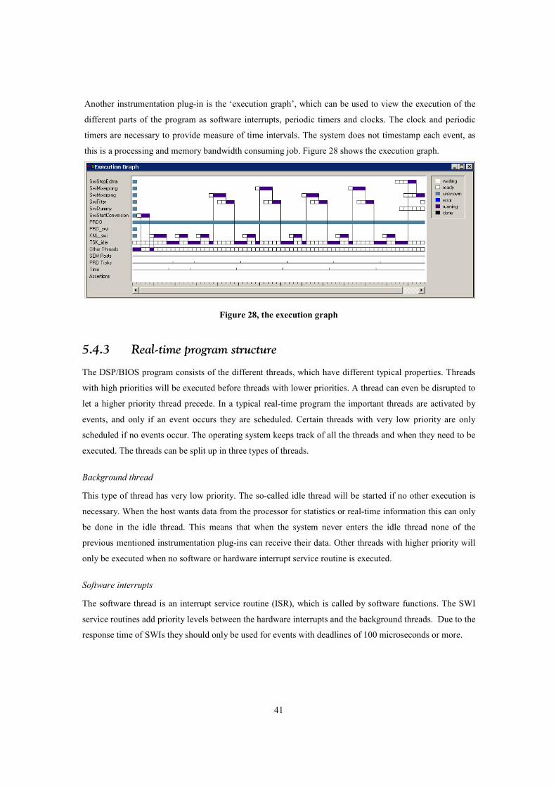
41
Another instrumentation plug-in is the ‘execution graph’, which can be used to view the execution of the
different parts of the program as software interrupts, periodic timers and clocks. The clock and periodic
timers are necessary to provide measure of time intervals. The system does not timestamp each event, as
this is a processing and memory bandwidth consuming job. Figure 28 shows the execution graph.
Figure 28, the execution graph
5.4.3 Real-time program structure
The DSP/BIOS program consists of the different threads, which have different typical properties. Threads
with high priorities will be executed before threads with lower priorities. A thread can even be disrupted to
let a higher priority thread precede. In a typical real-time program the important threads are activated by
events, and only if an event occurs they are scheduled. Certain threads with very low priority are only
scheduled if no events occur. The operating system keeps track of all the threads and when they need to be
executed. The threads can be split up in three types of threads.
Background thread
This type of thread has very low priority. The so-called idle thread will be started if no other execution is
necessary. When the host wants data from the processor for statistics or real-time information this can only
be done in the idle thread. This means that when the system never enters the idle thread none of the
previous mentioned instrumentation plug-ins can receive their data. Other threads with higher priority will
only be executed when no software or hardware interrupt service routine is executed.
Software interrupts
The software thread is an interrupt service routine (ISR), which is called by software functions. The SWI
service routines add priority levels between the hardware interrupts and the background threads. Due to the
response time of SWIs they should only be used for events with deadlines of 100 microseconds or more.

42
Hardware interrupts
Hardware events that occur in the DSP’s environment can trigger the ISR for the event. The hardware
interrupts are used for time critical events, and the ISR will be scheduled directly. Hardware interrupt
service routines can be processed quickly, but should be completed within 2 to 100 microseconds.
The software ISR is called when an SWI is posted. The sender can set some additional options in the
mailbox of the ISR. These options are checked before actually posting the SWI. This makes the software
ISR more flexible in its response to an SWI. The software ISR can, for example, be configured to be started
after a number of posts have been made. It can also be configured to be started when two other objects have
reported to be ready. If an SWI is posted twice, the choice can be made whether the ISR should be executed
twice or once. The SWI manager enables all these properties to be set and followed, which makes the SWIs
very flexible.
5.5 Software design
The approach to the beamforming system is closely related to software radio and therefore a large part of
the receiver and beamformer is implemented in software objects. The system uses the real-time operating
system DSP BIOS, as described in the previous section. This section will discuss the aspects of the system
design on software level and the different objects that can be found in the system. The system can be
described on two levels:
1. Thread level
2. Function level
The thread level is related to objects as real-time threads, which are part of the operating system. The
function level is related to low-level functions, which perform mathematical computations. This section
discusses the thread level design only, which consists of software objects for real-time purposes, and for
this a set of properties is described:
1. Name; specifies the name of the object
2. Event; specifies the event type that triggers the object.
3. Input variables; input of the object
4. Output variables; output of the object
5. SWI posts; the SWIs that can be posted by the object
6. Description; describes the functionality of the object
7. Function calls; low-level function calls;
Figure 29 shows the objects included in the system. Al objects are software interrupt service routines,
except the ‘Process buffer’ object.

43
Figure 29, software objects as part of the software-defined DDC and beamform algorithm
Start AD conversion
This object configures the AD converter and performs the programming of the EDMA controller. The
EDMA controller needs to be programmed to copy data from the AD converter and generate and interrupt
when ready.
Process buffer
This object is triggered by an external interrupt, generated by the EDMA controller. The EDMA controller
is configured to use two buffers, called a ping and a pong buffer. The process buffer object is a hardware
interrupt service routine, and its functionality is restricted. The routine checks whether the ping or pong
buffer is ready and depending on this it will start the DDC and beamforming objects.
DDC ping/pong
This object performs the actual downconversion of the channels. It operates either on the ping or the pong
buffer. The downconversion consists of mixers and a filters. The input is either the ping or pong buffer, and
its output consists of the I/Q signals for different channels.
Beamform
This object will perform the actual beamforming algorithm. For this the CM algorithm is used. The input is
consists of the I/Q signals for different channels. Its output is one I/Q signal representing the modulated
received signal. The following sections describe the thread level functionality, according to its properties.
Debug
The debug object is a thread that can be used for various debug functions. It can be used to halt the system,
by placing a breakpoint in the thread. The other objects can call the debug object when an error occurs, and
the system is halted. Special debug threads as this, with custom defined priorities, are useful, as the
system’s debugger only executes when the system is in idle mode.
In the next section the threads are discussed in more detail.

44
5.5.2 Start AD conversion
The EDMA controller is programmed to react on the external interrupt 4, which is connected to the AD
converter. If the interrupt occurs, the EDMA controller will copy the data from the ADC’s FIFO buffer to a
buffer in the internal memory of the DSP. The EDMA is programmed to copy the data subsequently to a
so-called ping and pong buffer. If the buffer reaches a defined value (for example. 512 values), a Transfer
Complete interrupt is generated. This will enable the software to react on the data in the buffer, which is
ready to be processed.
The EDMA controller will reload its parameter table, which contains a different destination address, to start
copying to the other buffer. The buffer is switched every time the Transfer Complete interrupt is generated.
The EDMA controller is programmed to use the global variables ad_buffer_ping and
ad_buffer_pong as ping and pong buffer. The buffers are interleaved, as the interleaving is done inside
the ADC’s FIFO buffer. No de-interleaving is performed and the data is copied directly from the FIFO to
the buffers by the EDMA controller. The properties of the object start AD conversion are given in the next
table.
SWI object StartConversion() Event None , called in main(); Input variables None Output variables ad_buffer_ping (global)
ad_buffer_pong(global) Description Part of the initialization. Programs the EDMA. Opens EDMA channel and starts the
conversion. SWI posts None Function calls edma_pingpong Status Implemented, tested.
5.5.3 Process ping or pong
When the EDMA controller completes its task, it will initiate an interrupt, called is the Transfer Complete
interrupt. Additionally it will set a number in the interrupt pending register. This number indicates whether
the ping or pong buffer is ready to be processed. The object for ‘process ping or pong’ is an HWI service
routine, responding to the Transfer Complete interrupt, and it will post the SWI for DDCping or -pong to
start the processing of respectively the ping or pong buffer. The function also posts the SWI for the object
‘Beamform’, which initiates the beamform algorithm. As both SWIs are defined by a priority, the system
will first execute the ‘DDC’ object (higher priority) followed by the ‘Beamform’ object.

45
HWI object Edma_HWI() Event Interrupt 8 (EDMA Transfer Complete interrupt) Input variables None Output variables
None
SWI posts &SwiDDCping or &SwiDDCpong &SwiBeamform
Description Reads the interrupt pending register, Determines ping or pong buffer ready, Clears interrupt pending register, Clears interrupt Starts the digital downconverter Starts the beamform
Function calls None Status Implemented, tested
5.5.4 DDCping/pong
The ‘DDCping’ and ‘DDCpong’ objects perform the downconversion. First the function
mixer2channel is called. Note that the official system would need 4 channels, this can be implemented
if the system is ready to perform beamforming for 4 channels. This function de-interleaves the data
(ad_buffer_ping or ad_buffer_pong) and multiplies them with cosine and sine functions. The
result is stored in intermediate buffers, which is subsequently processed by the FIR filter function fir_r8.
To enable continuous operation of the filter without disrupting the data as a consequence of the block input,
the state of the filter is stored and recalled when a block data is ready to be filtered. This is done by
firconfig and firrestore.
SWI object DDCping() or DDCpong() Event &SwiDDCping, &SwiDDCpong Input ad_buffer_ping or ad_buffer_pong (global) Output I1out, Q1out, I2out, Q2out (global) Description Reads interleaved data from the ad_buffer_ping,
Downconverts and de-interleaves data to I/Q signals per channel Function calls
Mixer Firconfig Fir_r8 Firrestore
Status Implemented for 2 channels, tested for 2 channels.

46
5.5.5 Beamform
This object performs the actual beamforming. Its input is the I/Q signals from different channels, and its
output is the beamformed I/Q signal. The resulting weight vectors (W) are stored for the next time that the
object is called. The low-level function that is called is the actual algorithm that performs the beamforming.
The beamforming is based on the Constant Modulus Algorithm and can be used to demonstrate suppression
of one interferer.
HWI object Beamform() Event &SwiBeamform Input variables I1out, Q1out, Q2out, Q2out, W (global) Output variables beamresI, beamresQ SWI posts None Description Performs beamforming Function calls Beamform Status Implemented, tested
5.6 Software to be implemented
The receiver is implemented partly. For example, demodulation is not implemented. The demodulation is
necessary to convert the output of the beamformer to a real bit-stream. In the case of the MSK signal, this
can be done as described in Chapter 4, by using a differential detector and a bit-clock recovery algorithm to
detect the optimum bit instant. When this part is implemented the system can be tested by performing bit
error rate (BER) calculations.
The use of the LMS algorithm requires a system where the reference signal is synchronized with the
system. This can only be done by using a known bit sequence, and after demodulation, a correlator is
necessary to find the sequence. When the correlator has found the start of the bit-sequence, the reference
vector could be aligned with received signal from the antenna array. When the reference vector is aligned
the system initiate the object for the LMS algorithm.
The current software structure is suitable for a demonstration of a simple software-defined radio
architecture. When a system gets more complex, the current implementation is not satisfying anymore. A
special framework is necessary to work within. This framework should specify how the software objects
are defined and how they should operate. Also the usage of inter-object communication and the usage of
data objects should be specified. In the current implementation there is no inter-object communication and
the data objects are global variables. If a time constraint is not met within the current system an object may
overwrite the data of another object, leading to disruption of the data. These are typical issues that should
be covered by a quality real-time framework.

47
6 Test results
This chapter1 will discuss the test results for the system. The parts that need to be tested are the software
objects and the overall functionality. The first of this chapter will show the results of the beamforming
systems performance and its functionality on thread level. In the second part the digital downconverter is
tested functionally. The third part describes the results for the complete system, including beamforming.
The following setup is used:
• Two function generators
• Two channels: each 521 kS/s
• ADC speed: 1042 kS/s
• IF frequency: 130250 Hz
• MSK modulated test vectors 130250 bps
A channel is one of the inputs of the quad-channel THS1206 ADC. The understanding ‘channel’ is also
used for a baseband I/Q representation of the input signal after downconversion.
6.1 Thread test results
For a fast functional analysis on thread level, the execution diagram is used. The execution diagram
displays all threads. The execution diagram does not indicate the exact time on which the threads are
executed. The timeline is not linear, and only the execution sequence is represented. This means that there
is no relation between the length of a part of the execution diagram and its time. For a timing analysis in
program cycles the SWI accumulators are used. The system is configured to use 2 channels. The ‘DDC’
object is called on ping and pong buffer. For stability reasons the beamform algorithm is only executed for
the DDC for the ping buffer. Figure 30, shows the result of the thread level test.
1 This chapter is rewritten after the first version of the report was finished. Additional work, for example
the implementation of the CM algorithm, and its test results have resulted in this chapter. Therefore a small
part of this chapter briefly discusses some implementation aspects.

48
Figure 30, execution diagram
In the execution diagram the white blocks indicate the posting of a software interrupt and the purple blocks
indicate that a thread is running. It is not possible to view HWIs or HWI service routines in the execution
diagram. Therefore the object ‘process buffer’ described in the previous chapter is not visible in the
execution diagram. The names of the object that start with ‘Swi’ are the software interrupts, which are
being posted to initiate its relevant function or thread. The threads that are coupled to the SWI are visible in
the execution diagram when they are executed. Objects as TSK_idle and KNL_swi are part of the operating
system.
First ‘SwiStartConversion’ is posted, and its service routine programs the EDMA and ADC. Then after a
while the object ‘SwiDDCping’ is posted, to start the digital downconversion of the ping buffer. Directly
after posting ‘SwiDDCping’, ‘SwiBeamform’ is posted. Due to priorities the thread ‘Beamform’ is
executed after the execution of the thread ‘DDCping’. Once the interrupt service routine for the pong buffer
(not visible in execution graph) is called ‘SwiDDCpong’ is posted. The program was configured to only
process the thread ‘Beamform’ for the ping buffer, in case it cannot meet its time constraints. The
execution graph shows that the DDCpong is called, before the ‘Beamform’ object is started. When the
DDCpong object is finished, the ‘Beamform’ object continues. This indicates that the ‘Beamform’ object is
not meeting its time constraints, as it continues after the ‘DDCpong’ object has been activated. The system
cannot function correctly, as the ‘DDCpong’ object has disrupted the data for the ‘Beamform’ object.
Continuous operation is not possible.
The system is configured to work in discontinuous mode, as visible in the execution graph in Figure 31.
The DDC pong object is never called, and therefor the data for the beamform algorithm is not disrupted
during operation. Note that this causes half of the data to be ‘dropped’ as the DDCpong object is not called
anymore. From the execution graph it is clear that time constraints are now met.

49
Figure 31, execution diagram
The program is configured to halt after processing 2 times the ‘ping’ buffer. On the fourth interrupt that
indicates that the pong buffer can be processed, the HWI service routine posts two software interrupts.
1. StopEdma
2. Dummy
‘StopEdma’ has the highest priority, and will shut down the EDMA controller. The data from the ADC is
no longer copied to the buffers and the Transfer Complete interrupts are no longer generated. ‘DDCpong’ is
not called to perform downconversion. The ‘Beamform’ object was interrupted by the ‘StopEdma’ object,
because its priority is higher. After the ‘StopEdma’ object is finished the ‘Beamform’ object continues.
When this object is ready, the thread with the lowest priority is called, ‘Dummy’, which is used to halt the
system on.
The execution graph indicates that the system performs stable on thread level, but doesn’t indicate the
performance of the system. This can be monitored by using the statistics manager. With the statistics
manager, every thread coupled to the SWIs, can be monitored. It displays the number of posts and the
number of instructions of the relevant thread. Custom statistics can be monitored too, by using special
statistics functions. The hardware interrupt routine, which responds to the EDMA, is monitored too. Figure
32 shows the statistics on all statistics objects. This threads related to the interrupt service routines are
visible. The EDMA service routine, which adds statistics on the interrupts, is indicated by ping and pong.
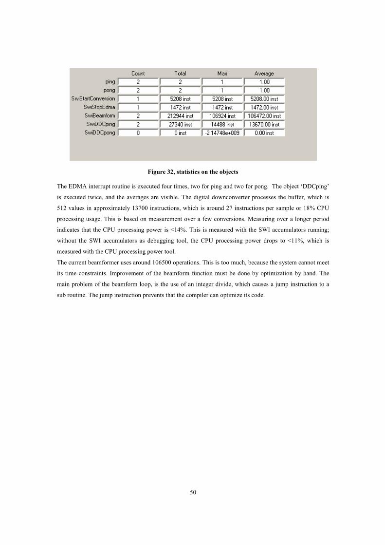
50
Figure 32, statistics on the objects
The EDMA interrupt routine is executed four times, two for ping and two for pong. The object ‘DDCping’
is executed twice, and the averages are visible. The digital downconverter processes the buffer, which is
512 values in approximately 13700 instructions, which is around 27 instructions per sample or 18% CPU
processing usage. This is based on measurement over a few conversions. Measuring over a longer period
indicates that the CPU processing power is <14%. This is measured with the SWI accumulators running;
without the SWI accumulators as debugging tool, the CPU processing power drops to <11%, which is
measured with the CPU processing power tool.
The current beamformer uses around 106500 operations. This is too much, because the system cannot meet
its time constraints. Improvement of the beamform function must be done by optimization by hand. The
main problem of the beamform loop, is the use of an integer divide, which causes a jump instruction to a
sub routine. The jump instruction prevents that the compiler can optimize its code.

51
6.2 Digital downconverter
The first step in the digital downconverter is the mixing of the interleaved data from the ping or pong
buffer. The next step is filtering the deinterleaved I and Q signals with a low pass filter. Two digital signal
generators generate the test vector. In Figure 33 the result for both channels is shown. Both pictures
indicate the I and Q component of the baseband signal. The first picture is the result of the DDC for the
first channel and the second picture is the result of the DDC for the second channel. The IF signals
generated for both channels are equal. It can be seen as a signal from one source, arriving at antenna
boresight. The test vector was a sequence of ones followed by a sequence of zeros. The point at around 120
indicates the point where the bitsequence is changed from ones to zeros. The Q channel makes a phase shift
of ½π. The disruption at the start and around sample 220 are caused by the signal generators, which are
synchronized in burst mode2. This results in a small disruption between the repeated sequence.
Figure 33, output of the digital downconverter for two channels, represented by I and Q components.
The MSK signal can be found back in the filtered result. The overall system phase is very stable, which can
be seen in the figures by the fact that the phase-shifts are ½π or -½π at every bit instant.
There is no noticeable phase difference between both channels, which indicates no severe phase lag
between the function generators. This has been verified on a digital oscilloscope. If a phase lag existed
between the function generators, this can be corrected by adjusting the phase of one of the generators
internally.
2 To synchronize two function generators, a third function generator was used, to generate synchronization
signals. Every time the third generator pulses the two other function generators, the arbitrary waveform is
‘played’. After the waveform is played, the function generators wait for the next sync pulse. This ‘wait’
causes a disruption in the generated signal.

52
When plotting the one of the outputs of the DDC into an X/Y plot Figure 34 is found, where every I and Q
sample pair of one of the channels in Figure 33 is plotted by a dot, representing the complex value. The
downconverted I/Q signal has a constant amplitude.
Figure 34, I/Q representation of the output of the DDC for one channel
6.3 Beamform algorithm
The CM algorithm was chosen to be implemented as it does not need synchronization compared with the
LMS algorithm. For the CM algorithm a modified error is used and (2.20) is modified to:
( )
( )( )2
y ny n
y nε = − (6.1)
The error is changed, where the modulus of y(n) is changed to a squared modulus. This removes the
required square root function for the calculation of the modulus. This square root function is slow and
prevents software pipelining by the compiler due to jump instructions, and should therefore not be used in
fast algorithms. Both (2.20) and (6.1) have proven to be stable algorithms in MATLAB tests.
The implementation of the beamform algorithm suffered from the unstable development environment,
which made the implementation process slow. Therefore a successful alternative was used to implement the
beamform functions. As the algorithm is not part of the real-time functionality of the system, it was first
implemented on a PC in Visual Studio, using linear debugging. This type of debugging is much faster and
simpler then the debugging on the DSP. For testing the functionality of the beamform function, MATLAB
was used to generate test vectors.
The function was implemented using integers only, for speed purposes. Integers are necessary as shorts are
to small due to accumulation and multiplication. For the implementation, it is very important that no
overflow is caused in the algorithm. The 32 bit integers have a range of -2147483648 and 2147483648.
This is not much as the algorithm requires many multiplies and some divides. This means that through the
algorithm, many elements need to be scaled. The scaling is done with bit shifts, as this functionality is
available in the DSP’s ALUs. This is faster then dividing or multiplying, but the factor for scaling is always
a power of 2.

53
This scaling is necessary, to prevent the algorithm to get unstable due to overflow or underflow. The actual
implementation of the algorithm is visible in Appendix C, in the section ‘beamform.c’. This C version was
compared to the MATLAB simulations and has been tested. The CM algorithm is only implemented for a
system with two antennas. Therefore the algorithm can only remove one interferer.
After the functional testing of the algorithm, the function has been transferred to the DSP software
environment, where the algorithm was added to the real-time system. The test setup for the system is as
followed:
1. Two function generators generate the signals for the two antennas
2. The function generators are synchronized by a third reference signal generator
3. There is one ‘desired’ signal
4. There is one ‘interfering’ signal
The signals which are received by the two antennas are generated by the file ‘arbgen2.m’. The function is
implemented for 2 antennas only. The function generators simulate the necessary IF frequencies, by using
the generated signals from MATLAB. Two experiments are carried out to demonstrate the beamforming
system.
6.3.1 Experiment 1
The first experiment demonstrates the beamform algorithm. Two signals are generated to simulate the two
antennas and receivers which are a combination of the signals specified in table 3. In the experiment both
the IF signals that are received are a combination of the desired and interfering signal, where the signals are
shifted in time (phase) to simulate the angle of arrival.
Desired Signal Interfering signal
MSK modulated signal MSK modulated signal
150 bit test vector 150 bit test vector
Long lengths with the same bits Frequent changes of bits
Arriving at zero degrees Arriving at angle of 18 degrees
Table 3 , specification of the signals
It has been shown that the beamform algorithm is not fast enough for continuous operation. If the
beamform algorithm is started sequentially to the ‘DDCping’ object, ‘DDCpong’ is started before the
beamform object is ready. Therefor the beamform algorithm is only executed once. The ‘DDCping’ object
is never started, because it will overwrite the data for the ‘Beamform’ object. Therefore the ‘Beamform’
algorithm is not running in a continuous matter in the experiment and the ‘DDCpong’ object is not called.
The system drops half of the data blocks, as ‘DDCpong’ is never started.
Two function generators are programmed with the appropriate signals. The desired signal is arriving at
antenna boresight, at an angle of zero degrees. This means that the desired signal is arriving in phase at

54
both the antennas. The interfering signal arrives at an angle of 18 degrees. After 256 samples the
beamformer results in an array output as in Figure 35, which shows the I and Q channels. This figure
respresents the output of the array, that is the result of the weight factors found by the beamform algorithm.
In Chapter 2.3, this signal is represented by y(t). The figure shows that the algorithm slowly converges.
However, the amplitude is not constant yet, which can be seen in the complex plane in Figure 36.
Figure 35, I /Q signal of array output after beamforming after over 256 samples
Figure 36, I/Q plot of array output after beamforming over 256 samples
The received signal is not an MSK signal, and still a combination of both received signals, the interferer
and desired signal.
If the system runs for a long period Figure 37 and Figure 38 are found. The signal that is shown is clearly
an MSK signal and in this case it is the signal that represents the slowly varying bit sequence. Around
sample 100, the phase shift in the I channel is clear which indicates that the signal is changing its run of
bits. The output shows a disruption around sample 192. This is due to the fact that at this point the signal
generators are synchronized, causing a disruption in both signals.
Figure 37, I/Q signal of array output after beamforming over 2560000 samples
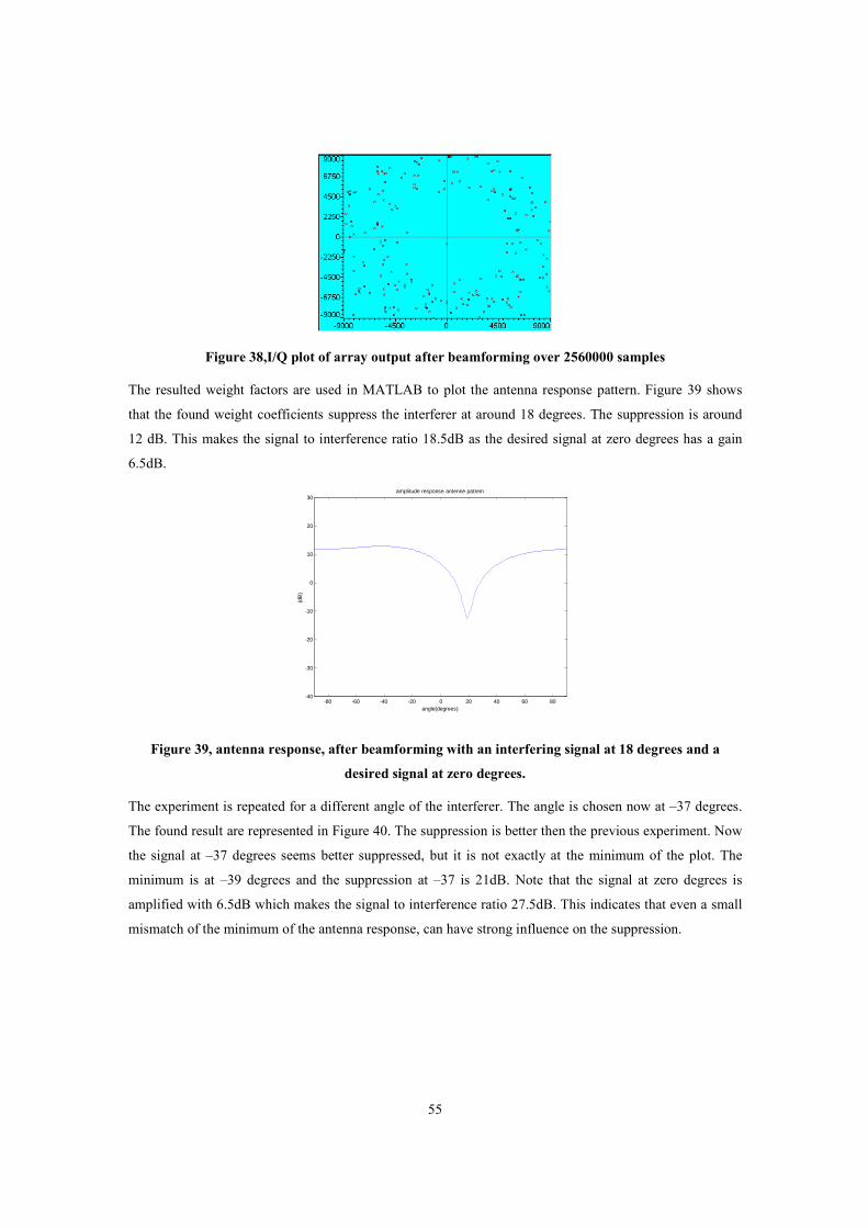
55
Figure 38,I/Q plot of array output after beamforming over 2560000 samples
The resulted weight factors are used in MATLAB to plot the antenna response pattern. Figure 39 shows
that the found weight coefficients suppress the interferer at around 18 degrees. The suppression is around
12 dB. This makes the signal to interference ratio 18.5dB as the desired signal at zero degrees has a gain
6.5dB.
-80 -60 -40 -20 0 20 40 60 80-40
-30
-20
-10
0
10
20
30amplitude response antenne pattern
(dB
)
angle(degrees)
Figure 39, antenna response, after beamforming with an interfering signal at 18 degrees and a
desired signal at zero degrees.
The experiment is repeated for a different angle of the interferer. The angle is chosen now at –37 degrees.
The found result are represented in Figure 40. The suppression is better then the previous experiment. Now
the signal at –37 degrees seems better suppressed, but it is not exactly at the minimum of the plot. The
minimum is at –39 degrees and the suppression at –37 is 21dB. Note that the signal at zero degrees is
amplified with 6.5dB which makes the signal to interference ratio 27.5dB. This indicates that even a small
mismatch of the minimum of the antenna response, can have strong influence on the suppression.

56
-80 -60 -40 -20 0 20 40 60 80-40
-30
-20
-10
0
10
20
30amplitude response antenne pattern
(dB
)
angle(degrees)
Figure 40 , antenna response, after beamforming with an interfering signal at –37 degrees and a
desired signal at zero degrees.
6.3.2 Experiment 2
In this experiment the same signals are used as in experiment 1 only the desired signal and the interfering
signal are swapped. This means that the signal that is arriving close to boresight needs to be suppressed and
the desired signal arrives at an angle of –2.5. To select the signal at –37 degrees, the spatial minimum as a
result of the initial weight vector is placed right from the interfering signal. The algorithm will converge to
the closest signal to be suppressed, which is the interfering signal at –2.5 degrees.
Interfering Signal Desired signal
MSK modulated signal MSK modulated signal
150 bit test vector 150 bit test vector
Long lengths with the same bits Frequent changes of bits
Ariving at antenna –2,5 degrees Arriving at angle of –37 degrees
The resulting signal with the weight coefficients found by the beamform algorithm is represented in Figure
41, represented by an I and Q component and as a complex vector in Figure 42. The figures show a rapid
changing signal which is an MSK modulated signal, with frequenct bit changes. The amplitude is less
constant but ‘open’ as visible in Figure 42.
Figure 41, resulting I and Q channels after beamforming
57
Figure 42, I /Q representation in the I/Q plane
If the found weight vectors are used to plot the antenna response pattern, Figure 43 shows the
corresponding antenna pattern. The antenna pattern has its minimum at –4, and at –2.5 the gain is around -
10 dB. Signal to interference ratio is therefore 16.5 dB.
-80 -60 -40 -20 0 20 40 60 80-40
-30
-20
-10
0
10
20
30amplitude response antenne pattern
(dB
)
angle(degrees)
Figure 43, antenna response, after beamforming with an interfering signal at –2.5 degrees and a
desired signal at –37 degrees
Both experiments indicate proper operation of the beamforming. With these experiments the concept of
beamforming is demonstrated in a real system. The system is only tested with an MSK signal; in further
experiments also other interferers must be considered to be tested. Only convergence of the algorithm was
demonstrated. The speed of the algorithm was not tested, and the number of samples used by the algorithm
was chosen very large, to be sure that the algorithm had converged. To test the quality of the system also
the speed of convergence must be tested in future tests.

58

59
7 Conclusions
The assignment definition “develop a smart antenna receiver that uses digital beamforming” was split up
into the sub-definitions in section 1.1:
1. Research the practical issues concerned with smart antennas
2. Implement a smart antenna test-bed or setup within a defined framework
3. Demonstrate the test-bed
The practical issues, which are concerned with the RF front-end, are researched. In Chapter 3 it is shown
that the heterodyne receiver is a good choice as an analog front-end for smart antennas. Its linearity for
phase and amplitude and the possibility to use IF sampling are the main reasons to chose this type of
receiver. The necessary analog products for the analog parts of the heterodyne receiver are available as
integrated circuits and evaluation modules. The actual implementation of the front-end requires a high
degree of expertise on this field. Therefore only a reference design proposal was made, using general-
purpose front-end components. Two algorithms are considered to be implemented; the Least Mean Square
algorithm and the Constant Modulus algorithm. The Constant Modulus Algorithm is simpler to implement
as it is a blind algorithm and it does not require synchronization.
The developed test-bed is designed according to the scope defined in section 1.1. The system is based on
digital beamforming, as the beamforming is done in the baseband on a digital signal processor. For the
system a real-time operating system is chosen called DSP/BIOS. The use of software objects enables
algorithm testing and development. A software-defined digital downconverter is used to translate IF signals
to the baseband. For the beamforming a CM algorithm is implemented. Details on the implementation of
the test-bed can be found in Chapter 5.
The current design and implementation include a driver for the AD converter based on the ping pong buffer
principle. Furthermore a multi-channel digital donwconverter is implemented. The performance of the
digital downconverter is satisfying. At a sample rate of 1 Ms/s, the digital downconverter uses less then 11
percent of the processing capacity of the DSP. The downconverter was tested for operation on two
channels. Note that for higher sampling rates, there is less processing power available for other algorithms
or software objects. The beamform algorithm demonstrated successful beamforming for two antennas, by
suppression of one interferer and receiving one desired signal. The system was only tested for two MSK

60
type signals. Selection of the desired MSK signal was possible by choosing the right initial weight vectors.
At thread level the beamforming algorithm could not meet its time constraints, and therefore the algorithm
could not be executed in continuous operation. Optimization by hand is necessary to improve the speed of
the algorithm on the DSP. Details on testing can be found in Chapter 6.

61
8 Recommendations
To test the performance of the system, bit error test must be used. To test the smart antenna system for bit
error rates, a demodulator is required as well as synchronization. The demodulator can be implemented by
using a differential detector and a bit clock recovery algorithm. Details on the detection of MSK signals can
be found in Chapter 4.
The system is only tested with an MSK type of interferer. The testbed can also be tested with other types of
interferers. The algorithms can be extended within the system to a maximum of 4 channels. For this 2 extra
programmable function generators are necessary.
The test-bed is used to demonstrate the concept of the smart antenna. This concept is demonstrated by a
rather simple software structure. For a more complex structure of real-time software objects a proper
software framework must be defined.

62

63
References
1. J. Litva, “Digital Beamforming in wireless communications”, 1996
2. G.Tsoulos, M.Beach, “Wireless Personal Communications for the 21st Century: European
Technological Advances in Adaptive Antennas” IEEE Communications Magazine, Sep. 1997.
3. J.B.Andersen, “Antenna Arrays in Mobile Communications: Gain, Diversity, and Channel Capacity”,
IEEE antennas and Propagation Magazine, Apr. 2000
4. T. Turletti, “GMSK in a nutshell”, Massachussets Institute of Technology, Apr. 1996.
5. S. Ponnekanti, “An overview of Smart Antenna Technology for Heterogeneous Networks”, IEEE
Communications Surveys, Fourth Quarter 1999
6. DECT Forum, “The DECT standard explained”, www.dect.ch, Feb 1997
7. R.H.Roy, “Application of Smart Antenna Technology in Wireless communication Systems”,
www.arraycomm.com
8. M. Loy, “Understanding and Enhancing Sensitivity in Receivers for Wireless Applications”, Texas
Instruments, Technical Brief, May 1999.
9. J.Min, “Analysis and Design of a Frequency-Hopped Spread-Spectrum Transceiver for Wireless
personal Communications”, Final Report, 1996
10. J.Razavilar, F Rashid-Farrokhi, K.J.Ray Liu, “Software Radio Architecture with Smart Antennas: A
Tutorial on Algorithms and Complexity”
11. B.Widrow, P.E.Mantey, L.J.Griffiths, “Adaptive Antenna Systems”, Proceedings of the IEEE, Dec.
1967
12. B. Junus, “RF Front-End Implementation Issues in Sofware-Defined Radio Receiver”, EE359 Project,
2000
13. S.Choi, H.J.Im, ”Implementation of a smart antenna test-bed for a wide-band CDMA mobile channel”
14. D.Grant, “Solving the Direct Conversion Problem”, www.planetanalog.com, Sep. 2000 *
15. M.Wennstrom, ”Smart Antenna Implementation Issues for Wireless Communications”, uppala
university, Oct 1999.
16. R.P. Lambert, “A Real-Time DSP GMSK Modem with All-digital Symbol Synchronization”, M. Sc.
Thesis, May 1998.
17. A. U. Aziz, “A Frequency Compensated Real-time DSP GMSK Modem”, M. Sc. Thesis, Aug. 1998.
18. L.R.Litwin, T.J. Endres, S.N. Hulyalkar, M.D. Zoltowski, “The effects of finite bit precision for a
VLSI implementation of the constant modulus algorithm”

64
19. S. Gummadi, B.L. Evans, “Cochannel signal separation in fading channels using a modified constant
modulus algorithm”
20. Texas Instruments, “Implementation of an adaptive antenna array using the TMS320C541”,
Application Report SPRA532.
21. National Semiconductor, “LMX3162 single chip radio receiver”, datasheet, Mar. 2000
22. Maxim, “Wireless Selection Guide”, 13th edition, 2001
23. Texas Instruments, “THS1206, THS12082, THS 10064, THS10082 Evaluation module”, may 2000
24. Texas Instruments, “Designing With the THS1206 High-speed Data Converter”, Apr. 2000
25. Texas Instruments, “THS1206 12-bit 6MSPS, Simultaneous sampling analog-to-digital converters,
May 1999
26. Texas Instruments, “TMS320C6000 Peripherals Reference Guide”, Feb. 2001
27. Texas Instruments, “TMS320C6000 Technical Brief”, Feb. 1999
28. Texas Instruments, “TMS320C6000 DSP/BIOS User’s Guide”, May 1999
29. Texas Instruments, “TMS320C62x/67x Programmer’s Guide”, May 1999
30. Texas Instruments, “Code Composer Studio, User’s Guide”, May 1999
31. Maxim, “Max2411A, Low-cost Up/Down converter with LNA and PA driver”, datasheet, 1998

65
Appendix A, Experiences with TI tools
The experiences and achievements with the development of software on the TI DSP platform and the use of
DSP/BIOS have leaded to insight in the system design approach in this environment. The general
experiences can be summarized as followed:
- The learning curve for the TI tools and DSP bios is very steep
- Functional programming should be done with linear debugging
- Real-time functionality of the DSP environment is not stable
The TI tools for DSP/BIOS are interesting to work with when designing functionality on thread level. For
designing algorithms on functional level the tools are less suited. This section will discuss the tools and
experiences and is followed with a proposal to develop
The drawbacks of software development with the real-time tools are listed below:
Visualization tools can only be used, when the exact effect on the software is known
One of the most important tools in the software environment is the so-called configuration manager. The
configuration manager provides a visual interface to all system configurations. The system needs to be
understood completely, before the visual interface is easy to work with. The configuration tool can be seen
as an interface for changing low level functionality. It is not a high level tool, and the smallest error in the
configuration can cause serious problems.
Thread level debugging depends on idle thread
When testing the thread level program, there are many reasons why an error can be caused. Most of the
errors occur when timing constraints are not reached. Instead of signaling the timing constraints the system
hangs on this type of error. If the SWI objects are stacking up, a stack overflow is easily reached. TI has
made its tools to take as little processing as possible. The so-called idle thread is called, when no other
activity is reported. This means that debugging at task level is only working when your system actually
performs satisfying! When timing constraints are not met, the system will never go into idle. This is strange
as debugging the real-time errors certainly becomes impossible. A workaround would be to develop a
custom debugging interrupt service routine that is coupled to a timer function on the processor. This means
that your system is having less power due to the debug overhead, but the system can be debugged better. If
this is done on regular occasion the system is more reliable, as it is performed always at the same time. If it
is a hardware interrupt routine, coupled to one of the DSP’s timer a very reliable debugging system could

66
be made. The interrupt routine must communicate with a host on the PC to transfer the necessary debug
information. All the TI hosts tools work through the idle thread. If debugging information needs to be
displayed on-screen, a custom host must be implemented. Threads need to be programmed now to
communicate with the debugger. The Real-time Data Exchange plug-ins could provide this functionality.
Real-time system crashes are severe
When the idle thread is never started, or a different problem induces a system hang, the resulting system
crash does severe damage to the stability of the tools and future performance of the DSP.
The system can be restarted by following the next procedure:
1. hard reset the DSP multiple times
2. software reset the DSP (to verify basic operation)
3. reload gel-file (initializes the necessary DSP peripherals)
4. restart program pointer
5. load the appropriate program
6. If the program cannot be loaded, repeat the above steps
7. If the program cannot be loaded, restart all tools, and turn DSP power off and on
If a program is loaded, it is still not certain if it will run properly. In many cases proper operation can be
derived from the fact that the system will halt on breakpoints. If the system is not halting on defined
breakpoints the program is still not functioning. In this case restarting tools and DSP is the best option.
A programmed EDMA controller causes also severe system crashes, if the EDMA is not reprogrammed to
shut down. Therefore it is always necessary to build an EDMA shutdown function that is called every time
you halt the system by brake points or by hand.
Due to these severe system crashes, debugging the software becomes a very intensive and slow task.
Thread level design and function level design must be separated
Designing at thread level and function level at the same time is not recommended. Function-level design
requires so-called linear debugging, which means that the functions are debugged by stopping at
breakpoints, to monitor if they work correctly. Combined by viewing the memory and monitoring variables
a function can be debugged. When the code functions correctly the function can be included at task level. If
errors occur now, it will not be because of the malfunctioning of the low level functions. Note that the
thread level debugging has certain short comings as stated earlier.

67
Appendix B, Matlab code
Demonstration of the LMS array, configured for 4 receivers. 2 Gaussian interferers are generated
and 1 desired MSK signal.
‘LMSarray.m’ %adaptive array demonstrator theta_x = 25 %degrees, direction of signal x theta_x = (2*pi/360)*theta_x theta_n1 = 0; %degrees, direction of noise source 1 theta_n1 = (2*pi/360)*theta_n1 theta_n2 = -40 %degrees, direction of noise source 2 theta_n2 = (2*pi/360)*theta_n2 theta = pi*[-1:0.005:1]; arraylength = 4; %nr of antennas bitrate = 100; fsim = 4*bitrate; %simulation frequency Ts = 1/fsim; %simulation sample period message = [1 -1 1 1 1 -1 1 -1 -1 -1 1 1 -1 1 -1 1 1 1 -1 -1 -1 1 1 1 1 1 -1 1 -1 1 1 1 -1 -1 -1 -1 1 -1 1 -1 -1 -1 -1 -1 1 1 1 -1 1 -1 1 1 1]; message = upsample(message, fsim/bitrate); %upsample message t = Ts:Ts:(length(message)/fsim); %timeline %%%%%%%%%%%%%%%%%%%%%%%%%%%%%%%%%%%%%%%%%%%%%%% %generate a complex MSK signal %%%%%%%%%%%%%%%%%%%%%%%%%%%%%%%%%%%%%%%%%%%%%%% mesint=(cumsum(message))/8; Q = cos(pi*mesint); I = sin(pi*mesint); plot(Q) hold on; plot(I,'r') signal_x = I+j*Q; %the signal to be received % the undesired complex noise singals-> uniform phase, gaussian amplitude distribution signal_n1 = normrnd(0,1,1,length(t)).*exp (j*(unifrnd(-pi,pi,1,length(t)))); signal_n2 = normrnd(0,1,1,length(t)).*exp (j*(unifrnd(-pi,pi,1,length(t)))); noise = zeros(arraylength, length(t)); % system noise for every antenna for i = 0:arraylength-1, noise(i+1,:) = normrnd(0,0.1,1,length(t)).*exp (j*(unifrnd(-pi,pi,1,length(t)))); end; %K = 2*pi/ lambda %d = 0.5*lambda %Kd means K*d equal to pi Kd = pi;

68
% array responses for the desired signal x and noise n1 and n2 arrayvec_x = zeros(1,arraylength); arrayvec_n1 = zeros(1,arraylength); arrayvec_n2 = zeros(1,arraylength); for k = 0:arraylength-1, arrayvec_x(k+1) = exp(j*k*Kd*sin(theta_x)); end; for k = 0:arraylength-1, arrayvec_n1(k+1) = exp(j*k*Kd*sin(theta_n1)); end; for k = 0:arraylength-1, arrayvec_n2(k+1) = exp(j*k*Kd*sin(theta_n2)); end; x = zeros(arraylength, length(t)); n1 = zeros(arraylength, length(t)); n2 = zeros(arraylength, length(t)); % received signal from signal source x for i = 0:arraylength-1, x(i+1,:) = signal_x .* arrayvec_x(i+1); end; % received signal from noise source n1 for i = 0:arraylength-1, n1(i+1,:) = signal_n1 .* arrayvec_n1(i+1); end; % received signal from noise source n2 for i = 0:arraylength-1, n2(i+1,:) = signal_n2 .* arrayvec_n2(i+1); end; %total received signal is the %+- -+ %| signal received at antenna 1 | %| signal received at antenna 2 | %| | | %| signal received at antenna n | %+- -+ signal_ns = (noise + n1+n2+x); % define weight vector w = zeros(1,arraylength); mu = 0.05; y = zeros(1,length(t));%output e = zeros(1,length(t));%error %%%%%%%%%%%%%%%%%%%%%%%%%%%%%%%%%%%%%%%%%%%%%%% %LMS Algorithm %%%%%%%%%%%%%%%%%%%%%%%%%%%%%%%%%%%%%%%%%%%%%%% for repeat=1:1,% use repeat for more convergence on the same message for i=0:length(t)-1, y(i+1) = w * signal_ns(:,i+1); e(i+1) = signal_x(i+1)-y(i+1); w = w + mu *e(i+1)*(signal_ns(:,i+1))'; end; end; %%%%%%%%%%%%%%%%%%%%%%%%%%%%%%%%%%%%%%%%%%%%%%% %Plot all figures %%%%%%%%%%%%%%%%%%%%%%%%%%%%%%%%%%%%%%%%%%%%%%% close all; subplot 311, (plot(phase(signal_x),':')) ylabel('phase(rad)'); %xlabel('sample(index)'); title('desired signal 25 degrees interferers 0 and -40 degrees')

69
hold on; plot(phase(y),'r'); legend('phase(d)','phase(y)') hold off; subplot 312, plot(abs(signal_x),':'); hold on; plot(abs(y),'r'); legend('|d|', '|y|') ylabel('amplitude'); %xlabel('sample(index)'); hold off; subplot 313, plot(abs(e)); legend('|error|'); ylabel('amplitude'); xlabel('sample(index)'); axis([0 210 0 1]); for k = 0:arraylength-1, arrayvec(k+1,:) = exp(j*k*Kd*sin(theta)); end; %calculate response of array F = w*arrayvec; figure plot(((theta/(2*pi))*360), 20*log10(abs(F))); title('amplitude response antenne pattern'); ylabel('(dB)'); xlabel('angle(degrees)'); axis([-90,+90,-30,10]); hold on; dbgrens = 40 %figure; plot(((theta/(2*pi))*360), phase(F)); %plot phase response if desired
The next MATLAB simulation demonstrates the use of the CM algorithm The same setup is used for
the simulation as the LMS algorithm, only the error is defined by a function based on the modulus of
the input signal.
FILE CMAarray.m
%adaptive array demonstrator CM algorithm
typeofinterferer1='noise'; %set to 'noise' for guassian type of interferer%set to 'signl' for
MSK type of interferer
theta_x = 10 %degreestheta_x = (2*pi/360)*theta_xtheta_n1 = -10; %degreestheta_n1 = (2*pi/360)*theta_n1
theta_n2 = -40 %degreestheta_n2 = (2*pi/360)*theta_n2
theta = pi*[-1:0.005:1];
arraylength = 4; %nr of antennas
bitrate = 100;fsim = 4*bitrate; %simulation frequencyTs = 1/fsim;message = [1 -1 1 1 1 -1 1 -1 -1 -1 1 1 -1 1 -1 1 1 1 -1 -1 -1 1 1 1 1 1 -1 1 -1 1 1 1 -1-1 -1 -1 1 -1 1 -1 -1 -1 -1 -1 1 1 1 -1 1 -1 1 1 1];
message = upsample(message, fsim/bitrate); %upsample messaget = Ts:Ts:(length(message)/fsim); %timeline
%%%%%%%%%%%%%%%%%%%%%%%%%%%%%%%%%%%%%%%%%%%%%%%%generate a complex MSK signal

70
%%%%%%%%%%%%%%%%%%%%%%%%%%%%%%%%%%%%%%%%%%%%%%%mesint=(cumsum(message))/8;Q = cos(pi*mesint);I = sin(pi*mesint);hold on;signal_x = I+j*Q; %the signal to be receivedsignal_ref = signal_x(1:end);
%%%%%%%%%%%%%%%%%%%%%%%%%%%%%%%%%%%%%%%%%%%%%%%%generate 2 interferers n1 and n2%%%%%%%%%%%%%%%%%%%%%%%%%%%%%%%%%%%%%%%%%%%%%%%
% if the interfere n1 needs to be gaussian noise -> uniform phase, normal amplitudedistributionif (typeofinterferer1 == 'noise'),signal_n1 = normrnd(0,1,1,length(t)).*exp (j*(unifrnd(-pi,pi,1,length(t))));end;
% if testing with an MSK signal as interferer is required: noise source n1 will be MSKsignalif (typeofinterferer1 =='signl'),message_n1 = [-1 -1 1 -1 1 -1 -1 1 -1 -1 -1 1 1 1 -1 -1 1 1 1 1 -1 1 -1 1 -1 1 -1 -1 -1 11 -1 1 -1 -1 -1 1 -1 1 -1 -1 -1 -1 -1 1 1 1 -1 1 -1 1 -1 -1];
message_n1 = upsample(message_n1, fsim/bitrate); %upsample messaget = Ts:Ts:(length(message)/fsim); %timeline
mesint_n1=(cumsum(message_n1))/8;Qn1 = cos(pi*mesint_n1);In1 = sin(pi*mesint_n1);signal_n1 = In1+j*Qn1; %the signal to be receivedend;
%noise source 2 is gaussiansignal_n2 = normrnd(0,1,1,length(t)).*exp (j*(unifrnd(-pi,pi,1,length(t))));
noise = zeros(arraylength, length(t));% system noise for every antennafor i = 0:arraylength-1,
noise(i+1,:) = normrnd(0,0.01,1,length(t)).*exp (j*(unifrnd(-pi,pi,1,length(t))));end;
%lambda = sym('lambda');%K = 2*pi/ lambda%d = 0.5*lambdaKd = pi;%alpha = -Kd*sin(theta_nul);
% array responses for the desired signal x and noise n1 and n2arrayvec_x = zeros(1,arraylength);arrayvec_n1 = zeros(1,arraylength);arrayvec_n2 = zeros(1,arraylength);
for k = 0:arraylength-1,arrayvec_x(k+1) = exp(j*k*Kd*sin(theta_x));
end;
for k = 0:arraylength-1,arrayvec_n1(k+1) = exp(j*k*Kd*sin(theta_n1));
end;
for k = 0:arraylength-1,arrayvec_n2(k+1) = exp(j*k*Kd*sin(theta_n2));
end;
x = zeros(arraylength, length(t));n1 = zeros(arraylength, length(t));n2 = zeros(arraylength, length(t));
% received signal from signal source xfor i = 0:arraylength-1,
x(i+1,:) = signal_x .* arrayvec_x(i+1);end;
% received signal from noise source n1for i = 0:arraylength-1,
n1(i+1,:) = signal_n1 .* arrayvec_n1(i+1);

71
end;
% received signal from noise source n2for i = 0:arraylength-1,
n2(i+1,:) = signal_n2 .* arrayvec_n2(i+1);end;
%total received signal is the%+- -+%| signal received at antenna 1 |%| signal received at antenna 2 |%| | |%| signal received at antenna n |%+- -+signal_ns = (noise + n1+n2+x);
%start weight vector, may be in the direction of the desired signal:w = (1/4)*[1, exp(-j*pi*sin(theta_x)),exp(-j*2*pi*sin(theta_x)),exp(-j*3*pi*sin(theta_x))];%start vector may be any type:%w = [0.1 0.1 0.1 0.1]wstart = w;%mu = 0.007;mu = 0.01;y = zeros(1,length(t));e = zeros(1,length(t));
%%%%%%%%%%%%%%%%%%%%%%%%%%%%%%%%%%%%%%%%%%%%%%%Constant Modulus Algorithm%%%%%%%%%%%%%%%%%%%%%%%%%%%%%%%%%%%%%%%%%%%%%%for repeat=1:1,
for i=0:length(signal_ref)-1,y(i+1) = w * signal_ns(:,i+1);%e(i+1) = 1 - y(i+1)e(i+1) = y(i+1)/((abs(y(i+1))))^2-y(i+1); %SATO's principle for updating the
errorw = w + mu*e(i+1)*(signal_ns(:,i+1))';
end;end;%%%%%%%%%%%%%%%%%%%%%%%%%%%%%%%%%%%%%%%%%%%%%%%%Plot all figures%%%%%%%%%%%%%%%%%%%%%%%%%%%%%%%%%%%%%%%%%%%%%%%close all;subplot 311, (plot(phase(signal_x),':'))ylabel('phase(rad)');
title('desired signal 10 degrees interferers -10 and -40 degrees')
hold on;plot(phase(y),'r');legend('phase(d)','phase(y)')hold off;
subplot 312, plot(abs(signal_x),':');hold on;plot(abs(y),'r');legend('|d|', '|y|')ylabel('amplitude');%xlabel('sample(index)');
hold off;subplot 313, plot(abs(e));legend('|error|');ylabel('amplitude');xlabel('sample(index)');axis([0 210 0 1]);for k = 0:arraylength-1,
arrayvec(k+1,:) = exp(j*k*Kd*sin(theta));end;%calculate response of arrayF = w*arrayvec;F2 = wstart*arrayvec;figureplot(((theta/(2*pi))*360), 20*log10(abs(F)));%hold on;%plot(((theta/(2*pi))*360), 20*log10(abs(F2)),'r');title('amplitude response antenne, desired signal: 10 degrees, interferers: -10 and -40degrees');ylabel('(dB)');xlabel('angle(degrees)');axis([-90,+90,-30,10]);

72
hold on;dbgrens = 40
MATLAB code demonstrating digital MSK signal generation and digital downconversion.
MODULATION modscr.m clear all;message = [0 -1 1 -1 1 -1 1 -1 1 -1 1 1 -1 1 -1 1 1 -1 -1 -1 1 1 -1 1 1 -1 -1 1 -1 1 -1 -1 1 1 1 1 1 -1 -1 1 -1 -1 1 -1 1 -1 1 1 -1 -1 -1 -1 1 -1 1 -1 1 1]; %message NRZ
bitrate = 100e3;carrier = 1e8;fr_dev = bitrate/4;fsim = 10*carrier; %simulation RF frequency
runtime = length(message)/bitrate;timeline = 0:1/fsim:runtime-1/fsim;
input = upsample(message, fsim/bitrate);
%actual modulation using VCO principleRF = vco(input,[carrier-fr_dev carrier+fr_dev], fsim);
DEMODULATION ddconv.m close all;Spb=4 %(approximate number of samples per bit)mu = 0.2;
fdown = 2500; %downsample ration relative to simulation frequencyfmis = 0; % mismatch in downconversion rateftot = fdown+fmis;
%heterodyne receiver structurelo = carrier + bitrate;losig = cos(2*pi*lo.*timeline); %create lo signaltransif = RF.*losig; %first demodulation stage
[b,a] = butter(5,0.1);IF = filter(b,a,transif);%lowpasfilter for removing images
normfreq = 0:1/(runtime*fsim):1-(1/(runtime*fsim));%semilogy(normfreq,abs(fft(IF)));
%%%%%%%%%%%%%%%%%%%%%%%%%%%%%%%%%%%%%%%%%%%%%%%%%%%%%%%% sampling the IF frequency%%%%%%%%%%%%%%%%%%%%%%%%%%%%%%%%%%%%%%%%%%%%%%%%%%%%%%%
IFs = IF(1:ftot:runtime*fsim); %downconvert using ftot
IFs = IFs*2;
%IQ demodulationI = IFs.*cos(2*pi*bitrate*(fdown/ftot)*timeline(1:ftot:end));Q = IFs.*sin(2*pi*bitrate*(fdown/ftot)*timeline(1:ftot:end));
I = 2*I;Q = 2*Q;%filter I and Q with 16 tap fir filterfirco = fir1(15,0.4);
I = conv(firco,I);Q = conv(firco,Q);
theta = 0;%differential detectionfor i = Spb+1:length(I),
Si(i) = I(i)*I(i-Spb)+Q(i)*Q(i-Spb);Sq(i) = Q(i)*I(i-Spb)-I(i)*Q(i-Spb);
end;S = (Si+j*Sq);e = zeros(1,length(Si));
phcor = zeros(length(Si)+1);phcor(1) = 0;Sicor = Si;

73
Sqcor = Sq;Scor = S;
%frequency compensation loopfor i = 1:length(Si)-1,
if Si(i) < 0.2,u = 1;
else,u = 0;
end;e(i) = -Sicor(i)*u*sign(Sqcor(i));phcor(i+1) = phcor(i) + mu*e(i);Scor(i+1) = S(i+1)*exp(-j*phcor(i+1));Sicor(i+1) = real(Scor(i+1));Sqcor(i+1) = imag(Scor(i+1));
end;
%bitclock recoveryfor i = Spb+1:length(Sicor),
tau(i)=Sqcor(i-Spb/2)*(sign(Sqcor(i))-sign(Sqcor(i-Spb))); %error functionend;
%correlatorfor i = 1:40,
corr(i) = [-1 1 -1 1 -1 1 -1 1 -1 1]*Sqcor(i:4:i+9*4)';end;[nietinteressant, index] = max(corr);clear nietinteressant;index%demodulateindices = zeros(1,length(message))mdec = zeros(1,length(message));%decoded messagemdec(1) = 0;for i = 2:length(message),
mdec(i) = sign(Sqcor(index));index = index - round(tau(index)*0.5)+4 %index updateindices(i) = index;
end;error = sum(abs(message - mdec))%number of errorsfigure;
hold on;plot(tau,'g:');plot(Sicor);plot(Si,':');plot(Sqcor,'r');plot(Sq,'r:');plot(indices,zeros(1,length(message)),'r*')legend('bitclock recovery signal', 'I corrected', 'I non-corrected','Q corrected', 'Qnon-corrected', 'strobe');
hold off;figure;plot(S);title('differential constellation, non-corrected')
figure;plot(Scor);title('differential constellation, corrected')
figure;hold on;plot(e);plot(phcor,'r');legend('error size', 'phase correction');
GENERATION OF THE TESTVECTORS FOR THE FUNCTION GENERATORS
Arbgen.m
clear all;%bitsequence onemessage = [1 1 1 1 1 1 1 1 1 1 1 1 1 1 1 1 1 1 1 1 1 1 1 1 1 1 1 1 -1 -1 -1 -1 -1 -1 -1 -1 -1 -1 -1 -1 -1 -1 -1 -1 -1 -1 -1 -1 -1 -1 1 1 1 1 1 1 1 1 1 1 1 1 1 1 1 1 1 1 1 1 1 1 11 1 1 1 1 -1 -1 -1 -1 -1 -1 -1 -1 -1 -1 -1 -1 -1 -1 -1 -1 -1 -1 -1 -1 -1 -1 1 1 1 1 1 1 11 1 1 1 1 1 1 1 1 1 1 1 1 1 1 1 1 1 1 1 1 -1 -1 -1 -1 -1 -1 -1 -1 -1 -1 -1 -1 -1 -1 -1 -1-1 -1 -1 -1 -1 -1]; %message NRZ%bitsequence twe
74
message2 = [1 -1 1 -1 1 1 -1 -1 -1 1 1 1 1 -1 1 1 -1 -1 -1 -1 1 1 -1 1 1 1 -1 1 1 -1 -1 -1 1 1 -1 1 1 -1 -1 -1 1 -1 1 -1 -1 -1 1 -1 1 -1 1 -1 -1 1 1 1 1 -1 1 -1 1 1 1 1 -1 -1 -11 -1 1 1 1 1 1 -1 1 1 1 -1 -1 -1 -1 -1 -1 -1 -1 1 1 -1 -1 -1 -1 1 1 1 -1 -1 1 -1 -1 1 1 1-1 -1 -1 -1 1 1 -1 1 1 -1 -1 1 1 -1 -1 -1 1 -1 -1 1 1 -1 -1 1 1 -1 1 -1 -1 1 -1 -1 -1 1 11 1 -1 -1 1 -1 1 -1 1 -1 -1 -1]
length(message)fsample =1042e3;nrchannels=2;fsample = fsample/nrchannelsbitrate = fsample/4;fIF = fsample/4;fr_dev = bitrate/4;
fsim = 100*fIF; %simulation RF frequency
runtime = length(message)/bitratetimeline = 0:1/fsim:runtime-1/fsim;
input = upsample(message, fsim/bitrate);input2 = upsample(message2, fsim/bitrate);
%actual modulation using VCO principle%RF is actually at IF frequency; RF is just a name for the variableRF = vco(input,[fIF-fr_dev fIF+fr_dev], fsim);%noise is the bitsequency that is interfering; in this case message2( or input2)noise = vco(input2, [fIF-fr_dev fIF+fr_dev], fsim);%%antenna 1 and antenna 2 and IF signals are shifted versions%to represent the angle at which they arriveRF1 = [RF(1:3),RF(4:end)+noise(1:end-3)];RF2 = [RF(1:25),RF(26:end)+noise(1:length(noise)-25)];
%normalizaing signalsnorm = max([max(abs(RF1)),max(abs(RF2))]);RF1 = RF1/norm;RF2 = RF2/norm;
%map on -2047 to +2047RF1 = round(2047*RF1);RF2 = round(2047*RF2);%display maximum for verificationmax(RF1)max(RF2)
generatorfrequency = 1/runtime%hpdata1 and hpdata2 are the files that can be uploaded to the HP function generatorsfid = fopen('hpdata1','w');for i = 1:length(RF1)-1,
fprintf(fid,'%d',RF1(i));fprintf(fid,',');
end;fprintf(fid,'%d',RF1(length(RF1)));fclose(fid)
fid = fopen('hpdata2','w');for i = 1:length(RF2)-1,
fprintf(fid,'%d',RF2(i));fprintf(fid,',');
end;fprintf(fid,'%d',RF2(length(RF2)));fclose(fid)

75
Appendix C, C source code
The project uses the following header files:
• firco.h
• ddc.h
The file firco.h describes the filter coefficients
The file ddc.h describes the data types for the digital downconverter.
The project is formed by the following source files:
• main.c
• ddc.c
• beamform.c
Additionally the following generated files of the AD converter plug-in are available:
• functions.c
• t1206_obj.c
• tidc_api.c
The generated files are left out of this section. For information the reader is referred to the ‘help’ of ‘Code
Composer Studio’ on the data converter plug-in.
The file main.c contains the task level threads. The threads are configured and prioritized by the
configureation manager.
The file ddc.c contains the functions necessary for the digital downconverter.
The file beamform.c contain the functions necessary for beamforming
The complete project for final version can be found on a cd-rom in the map /dsp/beamform3/
76
FILE ddc.h #define BLOCK_SZ 512#define FIRL 16#define CHANNELS 2
typedef struct{int real;int imag;}complex;
/*weight vector with two weights*/typedef struct{complex w1;complex w2;}beamvec;
/*data type for data that needs to be filtered by a fir_r8 function
*/typedef struct{
short data[(BLOCK_SZ/2)+FIRL-1];short *pstart;short *pdata;short *pend;
}firinputbl;
/*the state of a fir filter*/typedef struct{
short firstate[FIRL-1];}fir16;
/*function prototypes*/void initfirinputbl(firinputbl *firinputblobj);
void initfir(fir16 *firobj);
void firconfig(fir16 *firobj, firinputbl *inputblobj);
void firready(fir16 *firobj, firinputbl *inputblobj);
void mix2channel(short *inputstream, short *ch1I, short *ch1Q, short *ch2I, short *ch2Q);
void beamform(short *Iout, short *Qout, short *I1, short *Q1, short *I2, short *Q2,beamvec *wobj, const int length);
complex cxmult(const complex var1, const complex var2);
complex cxadd(const complex var1, const complex var2);
complex cxinprodcj(complex *var1, complex *var2, const int length);
complex cxinprod(complex *var1, complex *var2, const int length);
complex cxconj(const complex var1);
int cxreal(const complex var1);
int cximag(const complex var1);
void beamform2(complex *ch1, complex *ch2, complex* out, complex *w, int length);

77
FILE: ddc.c #include "firco.h"#include "ddc.h"
#define BUFFER_SZ 512
/***************************************************************************Function: initfirco()the function copies the the filter coefficients from the constants to avariable.
args: frc pointer to the destination variable for the filter coefficients***************************************************************************/void initfirco(short *frc){
short i;short *firco=frc;
for(i=0;i<(FIRL-1);i++){
*firco++ = fircoeff[i];}
}
/***************************************************************************Function: initfirinputbl()this function sets the pointers to the start, data and end section of theinputblock object.
args: firinputblobj pointer to the firinputblock***************************************************************************/void initfirinputbl(firinputbl *firinputblobj){
int i;firinputbl *finbl;short *startbl;
finbl = firinputblobj;startbl = finbl->data;
finbl->pstart = startbl;finbl->pdata = startbl+FIRL-1;finbl->pend = startbl+(BLOCK_SZ/2);
for (i=0;i<(BLOCK_SZ/2)+FIRL-1;i++)*startbl++ = 0;
}
/***************************************************************************Function: initfir()this function sets the fir state values of a fir16 object to zero
args: firinputblobj pointer to the firinputblock***************************************************************************/void initfir(fir16 *firobj){
short *ptrx;int i;ptrx = firobj->firstate;
for (i=0;i<(FIRL-1);i++){*ptrx++=0;}
}
/***************************************************************************Function: firconfig()firconfig is called before a fir function is called. It will copy the state

78
of the fir filter to the begin section of the firinputblock.
args: firobj pointer to the firobjectfirinputblobj pointer to the firinputblock
***************************************************************************/void firconfig(fir16 *firobj, firinputbl *inputblobj){
short *pstate, *pfirstart;int i;pstate = firobj->firstate;pfirstart = inputblobj->pstart;for(i=0;i<FIRL-1;i++)
*pfirstart++ = *pstate++;}
/***************************************************************************Function: firready()firconfig is called after a fir function is called. It will copy the endsection of the firinputblock to the state of the firobject.
args: firobj pointer to the firobjectfirinputblobj pointer to the firinputblock
***************************************************************************/void firready(fir16 *firobj, firinputbl *inputblobj){
short *pstate, *pfirend;int i;pstate = firobj->firstate;pfirend = inputblobj->pend;for(i=0;i<FIRL-1;i++)
*pstate++ = *pfirend++;}
/***************************************************************************Function: mix2channel()this function is used for mixer functionality on an input vector withinterleaved data for two channels.
args: inputstream pointer to the interleaved datalength BLOCK_SZ
ch1I pointer to output of mixer1 for inphase comp.length BLOCK_SZ/4
ch1Q pointer to output of mixer1 for quadr. comp.length BLOCK_SZ/4
ch2I pointer to output of mixer2 for in phase comp.length BLOCK_SZ/4
ch2Q pointer to output of mixer2 for quadr. comp.` length BLOCK_SZ/4
***************************************************************************/void mix2channel(short *inputstream, short *ch1I, short *ch1Q, short *ch2I, short *ch2Q){
short *input, *output1I, *output1Q, *output2I, *output2Q;short i;short channel1[4];short channel2[4];
input = inputstream;
output1I = ch1I;output1Q = ch1Q;output2I = ch2I;output2Q = ch2Q;
for (i=0;i<BUFFER_SZ/8; i++){
channel1[0] = ((*input) << 4) & 0xFFF0; /*use bitmask for 12 bits */channel2[0] = ((*(input+1)) << 4) & 0xFFF0;
channel1[1] = ((*(input+2)) << 4) & 0xFFF0;channel2[1] = ((*(input+3)) << 4) & 0xFFF0;
channel1[2] = ((*(input+4)) << 4) & 0xFFF0;channel2[2] = ((*(input+5)) << 4) & 0xFFF0;
channel1[3] = ((*(input+6)) << 4) & 0xFFF0;channel2[3] = ((*(input+7)) << 4) & 0xFFF0;
79
/*multiply with sine*/*(output1I) = 0;*(output1I+1) = channel1[1];*(output1I+2) = 0;*(output1I+3) = -1*channel1[3];/*multiply with cosine*/*(output1Q) = channel1[0];*(output1Q+1) = 0;*(output1Q+2) =-1*channel1[2];*(output1Q+3) = 0;/*multiply with sine*/*(output2I) = 0;*(output2I+1) = channel2[1];*(output2I+2) = 0;*(output2I+3) = -1*channel2[3];/*multiply with cosine*/*(output2Q) = channel2[0];*(output2Q+1) = 0;*(output2Q+2) = -1*channel2[2];*(output2Q+3) = 0;
output1I+=4;output1Q+=4;output2I+=4;output2Q+=4;input+=8;
}}
// extra functions for debugging only. Not used in demonstrationcomplex cxmult(const complex var1, const complex var2){
complex result;result.real = var1.real*var2.real-var1.imag*var2.imag;result.imag = var1.real*var2.imag+var1.imag*var2.real;return result;
}
complex cxadd(const complex var1, const complex var2){
complex result;result.real = var1.real + var2.real;result.imag = var1.imag + var2.imag;return result;
}
complex cxinprodcj(complex *var1, complex *var2, const int length){
complex addup, temp1, temp2;complex *pvar1, *pvar2;int i;addup.real = 0;addup.imag = 0;pvar1 = var1;pvar2 = var2;
for(i=0;i<length;i++){
//cout << " round " << i << endl;temp1 = addup;
//cout <<"temp1 " << temp1.real <<" " << temp1.imag <<endl;temp2 = cxmult(*pvar1, cxconj(*pvar2));//cout <<"pvar1 en 2 "<< pvar1->real <<" "<< pvar1->imag << " " <<pvar2-
>real<<" "<< pvar2->imag<<endl;//cout <<"temp2 "<< temp2.real <<" " << temp2.imag <<endl;
addup = cxadd(temp1, temp2);//cout <<"addup "<< addup.real <<" "<< addup.imag<<endl;pvar1++;pvar2++;
}return addup;
}
complex cxinprod(complex *var1, complex *var2, const int length){
complex addup, temp1, temp2;complex *pvar1, *pvar2;
80
int i;addup.real = 0;addup.imag = 0;pvar1 = var1;pvar2 = var2;
for(i=0;i<length;i++){
//cout << " round " << i << endl;temp1 = addup;
//cout <<"temp1 " << temp1.real <<" " << temp1.imag <<endl;temp2 = cxmult(*pvar1, *pvar2);//cout <<"pvar1 en 2 "<< pvar1->real <<" "<< pvar1->imag << " " <<pvar2-
>real<<" "<< pvar2->imag<<endl;//cout <<"temp2 "<< temp2.real <<" " << temp2.imag <<endl;
addup = cxadd(temp1, temp2);//cout <<"addup "<< addup.real <<" "<< addup.imag<<endl;pvar1++;pvar2++;
}return addup;
}
complex cxconj(const complex var1){
complex temp;temp.real = var1.real;temp.imag = -var1.imag;return temp;
}
int cxreal(const complex var1){
return var1.real;}int cximag(const complex var1){
return var1.imag;}
File beamform.c #include <math.h>#include "ddc.h"
#define BUFFER_SZ 512
/***************************************************************************Function: beamform()This function performs the beamform functionality on an input of twochannels.
args: I1 pointer to an input array with inphase signalchannel 1
Q1 pointer to an input array with quadrature signalchannel 1
I2 pointer to an input array with inphase signalchannel 2
Q2 pointer to an input array with quadrature signalchannel 2
Iout pointer to an output array with quadrature signalQout pointer to an output array with inphase signalwobj pointer to the object that contains the weightvectorslength length of the input and output arrays
***************************************************************************/
void beamform(short *Iout, short *Qout,short *I1,short *Q1,short *I2,short *Q2, beamvec*wobj, const int length){
81
int i;complex y, e, temp1, temp2, temp3, temp4, w1, w2, yshift, special, chan1, chan2;beamvec *w;int abser;/*Q is real*//*I is imaginary*/short *resI, *resQ;short *Qreal1, *Qreal2, *Iimag1, *Iimag2;
w=wobj;resI = Iout;resQ = Qout;Qreal1 = Q1;Qreal2 = Q2;Iimag1 = I1;Iimag2 = I2;
for(i = 0;i<length;i++){ w1 = w->w1;
w2 = w->w2;
chan1.real = *Qreal1;chan1.imag = *Iimag1;chan2.real = *Qreal2;chan2.imag = *Iimag2;
temp1.real = chan1.real * w1.real - chan1.imag* w1.imag;temp1.imag = chan1.real * w1.imag + chan1.imag* w1.real;temp2.real = chan2.real * w2.real - chan2.imag* w2.imag;temp2.imag = chan2.real * w2.imag + chan2.imag* w2.real;
y.real = temp1.real + temp2.real;//unscaled yy.imag = temp1.imag + temp2.imag;
yshift.real = y.real >> 16; //scaled version of yyshift.imag = y.imag >> 16;
abser = (yshift.real*yshift.real+yshift.imag*yshift.imag)>>10;//abs|y|^2if (abser == 0) abser = 1;
special.real = y.real/abser;special.imag = y.imag/abser;
e.real = special.real-yshift.real;e.imag = special.imag-yshift.imag;
chan1.real = chan1.real >> 2;chan1.imag = chan1.imag >> 2;chan2.real = chan2.real >> 2;chan2.imag = chan2.imag >> 2;
temp3.real = e.real*chan1.real + e.imag*chan1.imag;temp3.imag = -e.real*chan1.imag + e.imag*chan1.real;
temp4.real = e.real*chan2.real + e.imag*chan2.imag;temp4.imag = -e.real*chan2.imag + e.imag*chan2.real;
temp3.real = temp3.real >> 13;temp3.imag = temp3.imag >> 13;temp4.real = temp4.real >> 13;temp4.imag = temp4.imag >> 13;
w->w1.real = temp3.real + w1.real;w->w1.imag = temp3.imag + w1.imag;w->w2.real = temp4.real + w2.real;w->w2.imag = temp4.imag + w2.imag;
*resQ = yshift.real;*resI = yshift.imag;
resQ++;resI++;Qreal1++;Qreal2++;Iimag1++;Iimag2++;
}}
/*

82
alternative beamform function which operates on complex input and outputnot used in the demonstration. Only for debugging purposes.*/
void beamform2(complex *ch1, complex *ch2, complex *out, complex *w,int length){
complex y, yneg, e, temp1, temp2, w1, w2, chan1, chan2, temp4, temp5, special,yshift;
int i;int abser;for(i = 0; i< length; i++){
//cout << "i = " << i<<endl;w1 = *w;w2 = *(w+1);chan1 = *ch1;chan2 = *ch2;
temp1 = cxmult(chan1,w1);temp2 = cxmult(chan2,w2);
y = cxadd(temp1, temp2);
yshift.real=y.real>>16;yshift.imag=y.imag>>16;
yneg.real=-yshift.real;yneg.imag=-yshift.imag;
abser = (yshift.real*yshift.real+yshift.imag*yshift.imag)>>10;
if (abser == 0) abser = 1;
special.real = y.real/abser;special.imag = y.imag/abser;
e = cxadd(special, yneg);
chan1.real = chan1.real >> 2;chan1.imag = chan1.imag >> 2;chan2.real = chan2.real >> 2;chan2.imag = chan2.imag >> 2;
temp4 = cxmult(e, cxconj(chan1));temp5 = cxmult(e, cxconj(chan2));
temp4.real = temp4.real >> 13;temp4.imag = temp4.imag >> 13;temp5.real = temp5.real >> 13;temp5.imag = temp5.imag >> 13;
*w = cxadd(w1,temp4);*(w+1) = cxadd(w2, temp5);
ch1++;ch2++;
}}
83
FILE main.c /****************************************************************/
/****************************************************************/
/****************************************************************//* include files*//****************************************************************/
#include <stdlib.h>/* include files for DSP/BIOS */#include <std.h>#include <swi.h>#include <log.h>/* include files for data converter (A/D convertor) support */#include "dc_conf.h"#include "t1206_fn.h"/* include files for chip support library */#include <csl.h>#include <irq.h>#include <timer.h>/*include files for the digital downconverter*/#include "ddc.h"#include <fir_r8.h>
/****************************************************************/// Definitions of global variables/****************************************************************/short ad_buffer[2*BLOCK_SZ]; /* global buffer for AD data */short *ad_buffer_ping ;short *ad_buffer_pong ;
short firr8[16];short *firc;
firinputbl I1;firinputbl Q1;firinputbl I2;firinputbl Q2;
firinputbl *pI1;firinputbl *pQ1;firinputbl *pI2;firinputbl *pQ2;
fir16 firI1;fir16 firI2;fir16 firQ1;fir16 firQ2;
short I1out[BLOCK_SZ/2];short Q1out[BLOCK_SZ/2];short I2out[BLOCK_SZ/2];short Q2out[BLOCK_SZ/2];
short beamresI[BLOCK_SZ/2];short beamresQ[BLOCK_SZ/2];
beamvec W;beamvec *wvec;int cnt=0;
struct EDMAh{EDMA_HANDLE channel;EDMA_HANDLE ping;EDMA_HANDLE pong;
} EDMAhandles;
/****************************************************************//* DSP/BIOS objects, created with the Config Tool *//****************************************************************/extern LOG_Obj trace;extern far SWI_Obj SwiStartConversion;extern STS_Obj ping;extern STS_Obj pong;extern far SWI_Obj SwiStopEdma;extern far SWI_Obj SwiBeamform;extern far SWI_Obj SwiDummy;

84
extern far SWI_Obj SwiDDCping;extern far SWI_Obj SwiDDCpong;/****************************************************************//* function prototypes *//****************************************************************/TIMER_HANDLE init_timer0(unsigned int period);void init_dsk(void);void edma_pingpong(void *pDC, void *pping, void *ppong, unsigned long ulCount);void init_HWI(void);void edma_stop();/****************************************************************//* The main program *//****************************************************************/void main(){
TIMER_HANDLE hTimer;ad_buffer_ping = &ad_buffer[0];ad_buffer_pong = ad_buffer_ping + BLOCK_SZ;
/*initialize weight vectors*/W.w1.real=1;
W.w1.imag=1;W.w2.real=1;W.w2.imag=1;
wvec = &W;
pI1 = &I1;pQ1 = &Q1;pI2 = &I2;pQ2 = &Q2;firc = &firr8[0];/* CSL_Init - required for the CSL functions of the driver */CSL_Init();
LOG_printf(&trace, "CSL init");/* initialize the DSK and timer 0 */init_dsk();LOG_printf(&trace, "DSK init");hTimer = init_timer0(ADC1_TIM_PERIOD);/* configure the data converter */dc_configure(&Ths1206_1);/* start the timer */TIMER_Start(hTimer);LOG_printf(&trace, "A/D convertor init");
init_HWI();/*initializing firs, firo and firobjects*/initfir(&firI1);initfir(&firI2);initfir(&firQ1);initfir(&firQ2);
initfirco(firc);
initfirinputbl(pI1);initfirinputbl(pI2);initfirinputbl(pQ1);initfirinputbl(pQ2);
/*Go!*/SWI_post(&SwiStartConversion);
}
void init_HWI(void){ /* Find EVT_names in IRQ doc's
in CSL Ref Guide*/IRQ_Map(IRQ_EVT_EDMAINT,8); /* Map EDMA interrupt */IRQ_Enable(IRQ_EVT_EDMAINT); /* Enable EDMA interrupt */HWI_enable(); /* Global int enable */
}
/****************************************************************//* SwiStartConversionFunc *//* This software interupt starts a new conversion using the *//* dc_rblock function. *//****************************************************************/
void StartConversionFunc(){
edma_pingpong(&Ths1206_1, ad_buffer_ping, ad_buffer_pong, BLOCK_SZ);}
85
/*The hardware interupt service routine.Responds to interupt 8 EDMA Tranfer Complete*/#pragma FUNC_EXT_CALLED (edma_HWI);
void edma_HWI(void){
int EDMA_Channel = 0;
EDMA_Channel = HEDMA_CIPR_GET(HEDMA_CIPR_ADDR);
/* vier*/if ((EDMA_Channel & 0x0010))
{STS_add(&ping, 1); /*add statistics*/EDMA_CIPR = 0x0010; /*clear pending register*/cnt++;if (cnt == 0) /*cnt = 0, loop forever*/
/*cnt = N, loop untill N interrupts*/{SWI_post(&SwiStopEdma);SWI_post(&SwiDummy);}
SWI_post(&SwiDDCping);}/*vijf*/else if ((EDMA_Channel & 0x0020)){ STS_add(&pong,1); /*add statistics*/
EDMA_CIPR = 0x0020; /*clear pending register*/cnt++;if (cnt == 0){
SWI_post(&SwiStopEdma);SWI_post(&SwiDummy);
}SWI_post(&SwiDDCpong);
}
}
/****************************************************************//* PeriodFunc *//* The function will be called every second by DSP/BIOS and *//* posts a StartConversion SWI to start a new conversion. *//****************************************************************/
/* UNUSED !!!!!!!!!!! */void PeriodFunc(){// static int cnt=0;
// LOG_printf(&trace, "Period: %d",cnt++);// SWI_post(&SwiStartConversion);}
/*stops the edma controller*/far void stop_edma(){
EDMA_DisableChannel(EDMAhandles.channel);EDMA_Close(EDMAhandles.channel);EDMA_FreeTable(EDMAhandles.ping);EDMA_FreeTable(EDMAhandles.pong);//SWI_post(&SwiDummy);
}
/*digital downconversion on pingbuffer*/void DDCping(){
/*mixer for 2 channels*/mix2channel(ad_buffer_ping, pI1->pdata , pQ1->pdata, pI2->pdata, pQ2->pdata);
/*configure data for filtering*/firconfig(&firI1, pI1);firconfig(&firQ1, pQ1);firconfig(&firI2, pI2);firconfig(&firQ2, pQ2);/*filter all channels */fir_r8(pI1->pstart,firc,&I1out[0],16,256);

86
fir_r8(pQ1->pstart,firc,&Q1out[0],16,256);
fir_r8(pI2->pstart,firc,&I2out[0],16,256);fir_r8(pQ2->pstart,firc,&Q2out[0],16,256);/*restore states of fir filter*/firready(&firI1, pI1);firready(&firQ1, pQ1);firready(&firI2, pI2);firready(&firQ2, pQ2);
}void DDCpong(){
mix2channel(ad_buffer_pong, pI1->pdata , pQ1->pdata, pI2->pdata, pQ2->pdata);
firconfig(&firI1, pI1);firconfig(&firQ1, pQ1);firconfig(&firI2, pI2);firconfig(&firQ2, pQ2);
fir_r8(pI1->pstart,firc,&I1out[0],16,256);fir_r8(pQ1->pstart,firc,&Q1out[0],16,256);
fir_r8(pI2->pstart,firc,&I2out[0],16,256);fir_r8(pQ2->pstart,firc,&Q2out[0],16,256);
firready(&firI1, pI1);firready(&firQ1, pQ1);firready(&firI2, pI2);firready(&firQ2, pQ2);
}
/*beamform function*/void Beamform(){
beamform(&beamresI[0], &beamresQ[0], &I1out[0], &Q1out[0], &I2out[0], &Q2out[0],wvec);}
void Dummy(){//insert breakpoint}
/*THS1206 CUSTOM functions!*//*programms the EDMA for ping pong buffering !!!!!!!!!!!!!!!!!*/
void edma_pingpong(void *pDC,void *pping,void *ppong,unsigned long ulCount)/* void (*callback) (void *) */
{EDMA_HANDLE hEdma,hping, hpong, hstop;UINT32 Opt,XfrCnt,Idx,Rld,DstAddr,SrcAddr;TTHS1206 *pAdc = pDC;
hEdma = EDMA_Open(pAdc->IntNum,EDMA_OPEN_RESET);if (!hEdma)
return;/*allocate reload registers*/hping = EDMA_AllocTable(-1);if (!hping){
EDMA_Close(hEdma);return;
}
hpong = EDMA_AllocTable(-1);if (!hpong){
EDMA_Close(hEdma);return;
}hstop = EDMA_AllocTable(-1);if (!hstop){
EDMA_Close(hEdma);return;
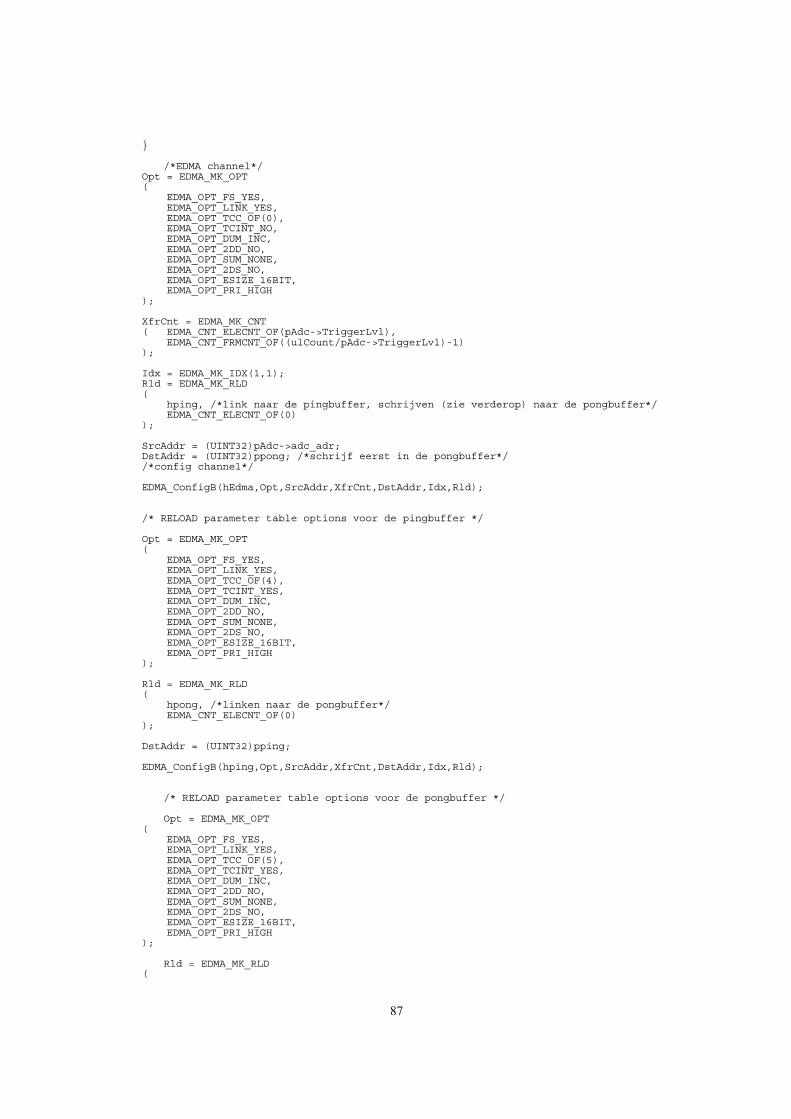
87
}
/*EDMA channel*/Opt = EDMA_MK_OPT(
EDMA_OPT_FS_YES,EDMA_OPT_LINK_YES,EDMA_OPT_TCC_OF(0),EDMA_OPT_TCINT_NO,EDMA_OPT_DUM_INC,EDMA_OPT_2DD_NO,EDMA_OPT_SUM_NONE,EDMA_OPT_2DS_NO,EDMA_OPT_ESIZE_16BIT,EDMA_OPT_PRI_HIGH
);
XfrCnt = EDMA_MK_CNT( EDMA_CNT_ELECNT_OF(pAdc->TriggerLvl),
EDMA_CNT_FRMCNT_OF((ulCount/pAdc->TriggerLvl)-1));
Idx = EDMA_MK_IDX(1,1);Rld = EDMA_MK_RLD(
hping, /*link naar de pingbuffer, schrijven (zie verderop) naar de pongbuffer*/EDMA_CNT_ELECNT_OF(0)
);
SrcAddr = (UINT32)pAdc->adc_adr;DstAddr = (UINT32)ppong; /*schrijf eerst in de pongbuffer*//*config channel*/
EDMA_ConfigB(hEdma,Opt,SrcAddr,XfrCnt,DstAddr,Idx,Rld);
/* RELOAD parameter table options voor de pingbuffer */
Opt = EDMA_MK_OPT(
EDMA_OPT_FS_YES,EDMA_OPT_LINK_YES,EDMA_OPT_TCC_OF(4),EDMA_OPT_TCINT_YES,EDMA_OPT_DUM_INC,EDMA_OPT_2DD_NO,EDMA_OPT_SUM_NONE,EDMA_OPT_2DS_NO,EDMA_OPT_ESIZE_16BIT,EDMA_OPT_PRI_HIGH
);
Rld = EDMA_MK_RLD(
hpong, /*linken naar de pongbuffer*/EDMA_CNT_ELECNT_OF(0)
);
DstAddr = (UINT32)pping;
EDMA_ConfigB(hping,Opt,SrcAddr,XfrCnt,DstAddr,Idx,Rld);
/* RELOAD parameter table options voor de pongbuffer */
Opt = EDMA_MK_OPT(
EDMA_OPT_FS_YES,EDMA_OPT_LINK_YES,EDMA_OPT_TCC_OF(5),EDMA_OPT_TCINT_YES,EDMA_OPT_DUM_INC,EDMA_OPT_2DD_NO,EDMA_OPT_SUM_NONE,EDMA_OPT_2DS_NO,EDMA_OPT_ESIZE_16BIT,EDMA_OPT_PRI_HIGH
);
Rld = EDMA_MK_RLD(

88
hping,EDMA_CNT_ELECNT_OF(0)
);DstAddr = (UINT32)ppong;
EDMA_ConfigB(hpong,Opt,SrcAddr,XfrCnt,DstAddr,Idx,Rld);
/* hstop */
Opt = 0;XfrCnt = 0;
EDMA_ConfigB(hstop,Opt,SrcAddr,XfrCnt,DstAddr,Idx,Rld);/*interupt enable register*/EDMA_CIER |= 1 << 5;
EDMA_CIER |= 1 << 4;
/* store information in TTHS1206 structure *//* daar hebben we op zich niet veel aan */pAdc->dc_edma = hEdma;pAdc->dc_table = hping;pAdc->CallBack = 0;
*(pAdc->adc_adr) = (pAdc->creg1.value | T1206_FRST | 0x400)<< pAdc->data_shift;
EDMAhandles.channel = hEdma;EDMAhandles.ping = hping;EDMAhandles.pong = hpong;
EDMA_ClearChannel(hEdma);EDMA_EnableChannel(hEdma);
}

89
Appendix D, Technology updates
By request of the supervisors, this section contains the Technology updates. These updates were used
during the meetings to evaluate problems and progress. The relevant updates contain interesting
information on the search for RF consumer products, which is the reason to include the updates in this
report. The updates are in Dutch.