development of a parallel image processing architecture in...
TRANSCRIPT

Development of a Parallel Image ProcessingArchitecture in VHDL
Stephen RoseSupervisor: Prof Thomas Bräunl
1st June 2012

Abstract
Image processing tasks such as filtering, stereo correspondence and feature detec-tion are inherently highly parallelisable. The use of FPGAs (Field ProgrammableGate Arrays), which can be operated in highly parallel configurations, can thusbe a useful approach in imaging applications. Many image processing tasks fallunder the category of SIMD (Single Instruction Multiple Data) operations, whichare a weakness of conventional CPUs, leading to the application of technologiessuch as FPGAs, Graphics Processing Units (GPUs), and Digital Signal Processors(DSPs) [1, 2]. The programmable blocks of an FPGA, and their interconnections,can be configured to optimise the device’s performance at specific tasks. Thismeans that commodity FPGAs can approach the speed of ASICs (ApplicationSpecific Integrated Circuits) in these applications, while retaining far greater flex-ibility. For embedded systems in particular, this performance can enable rapid vis-ion processing that would be impossible on standard embedded microprocessors[3, 4].
This project has focussed on the development of a synthesisable VHDL designsuitable for use as a general purpose image co-processor. In this approach, theFPGA’s Logic Blocks (CLBs) are allocated to discrete Processing Elements (PEs)that are connected in a grid configuration. Each PE corresponds to a single pixelof the target image, simplifying the adaptation of common image processing al-gorithms. The results of this implementation suggest that while theoretically, sucha design has significant advantages, current FPGA hardware is insufficient for thereal-world application of this general-purpose system at high resolutions.
iii

Acknowledgements
I would like to extend my thanks to Professor Dr. Thomas Bräunl for his ongoingassistance and supervision, as well as for providing the opportunity to work onsuch an interesting topic.
I would also like to thank FAHSS IT for allowing me such flexibility to deal withmy study and research obligations.
Finally, I would like to thank my family and friends for their patience and supportnot only through this year, but through my entire time at UWA.
iv

Contents
1 Background 11.1 Image Processing . . . . . . . . . . . . . . . . . . . . . . . . . . 11.2 FPGAs . . . . . . . . . . . . . . . . . . . . . . . . . . . . . . . . 1
1.2.1 Logic Area . . . . . . . . . . . . . . . . . . . . . . . . . 21.2.2 Operating Clock Speed . . . . . . . . . . . . . . . . . . . 3
1.3 HDLs . . . . . . . . . . . . . . . . . . . . . . . . . . . . . . . . 31.3.1 VHDL . . . . . . . . . . . . . . . . . . . . . . . . . . . 4
1.4 Higher Level Approaches . . . . . . . . . . . . . . . . . . . . . . 4
2 The Architecture 52.1 Processing Elements . . . . . . . . . . . . . . . . . . . . . . . . 5
2.1.1 Inputs and Outputs . . . . . . . . . . . . . . . . . . . . . 62.1.2 Internal Signals . . . . . . . . . . . . . . . . . . . . . . . 82.1.3 Choice of Instruction Set . . . . . . . . . . . . . . . . . . 9
2.2 The Processing Array . . . . . . . . . . . . . . . . . . . . . . . . 92.2.1 VHDL Generation of the Array . . . . . . . . . . . . . . 11
3 Exploration of Image Processing Tasks 153.1 Loading the Processing Array . . . . . . . . . . . . . . . . . . . 153.2 Reduction Operations . . . . . . . . . . . . . . . . . . . . . . . . 18
3.2.1 Finding the Array Maximum . . . . . . . . . . . . . . . . 183.3 Simple Image Filtering . . . . . . . . . . . . . . . . . . . . . . . 20
3.3.1 Mean Filtering . . . . . . . . . . . . . . . . . . . . . . . 203.3.2 Median Filtering . . . . . . . . . . . . . . . . . . . . . . 223.3.3 Sobel Operator . . . . . . . . . . . . . . . . . . . . . . . 25
3.4 Stereo Vision . . . . . . . . . . . . . . . . . . . . . . . . . . . . 293.4.1 Sum of Absolute Differences . . . . . . . . . . . . . . . . 30
3.5 Demonstration of Conditional Activation . . . . . . . . . . . . . . 32
4 Results 34
v

5 Conclusion 37
6 Future Work 386.1 Hardware Implementation . . . . . . . . . . . . . . . . . . . . . 386.2 Camera Interfacing . . . . . . . . . . . . . . . . . . . . . . . . . 396.3 Conditional Logic . . . . . . . . . . . . . . . . . . . . . . . . . . 396.4 Connection Changes . . . . . . . . . . . . . . . . . . . . . . . . 39
References 41
A PEs.vhd 46
B PA.vhd 52
vi

Abbreviations Used
ASIC Application Specific Integrated Circuit
CLB Configurable Logic Block
CPU Central Processing Unit
DDR Double Data Rate SDRAM
DSP Digital Signal Processor
FILO First In Last Out
FPGA Field Programmable Gate Array
HDL Hardware Design Language
IC Integrated Circuit
ISE Integrated Software Environment
LUT Lookup Table
PA Processing Array
PE Processing Element
RTL Register-Transfer Level
SIMD Single Instruction Multiple Data
VHDL VSIC Hardware Design Language
VSIC Very-high Speed Integrated Circuit
vii

1 Background
The aim of this project is to design and implement a highly-parallel image pro-cessing architecture in VHDL, suitable for implementation on a Xilinx Field-Programmable Gate Array (FPGA). The eventual implementation is for real-timeimage processing to take place on the FPGA device, then for processed inform-ation to be communicated to a central processor for display and actioning. Thisproject covers the initial VHDL implementation of a general purpose image co-processor. The architecture itself, as well as the implemented instruction set is dis-cussed, and simulated examples are used to demonstrate the capabilities of sucha system at accomplishing common image processing tasks. The results of thedesign synthesis are then explored, along with the ramifications of these results.
1.1 Image Processing
Vision processing is an application than can benefit significantly from parallelisa-tion, with similar or identical steps having to be performed on each pixel or blockof pixels that make up each image. This is especially true for what is known aslow-level image processing operations [5, 6]. For these low-level operations thatdo only operate on neighbouring pixels, the use of a mesh connected processingarray can achieve a very high level of performance[7]. There are also dedicatedSIMD processors which offer significant image-processing parallelism, at highspeeds, but with significantly less flexibility than an FPGA-based approach [8].
1.2 FPGAs
Field Programmable Gate Arrays are hardware units that can be reconfigured toperform a variety of digital logic functions. While Field Programmable Gate Ar-rays (FPGAs) may not achieve the performance of dedicated hardware, this tech-nology avoid the onerous costs of fabrication for small-run integrated circuits [9].FPGAs also have other benefits, offering a significant degree of flexibility through
1

the design process, such as a choice of Hardware Description Languages (HDLs),and a tight design loop, as repeated design iterations do not require physical fab-rication or reconfiguration[10]. There is also the potential for field reprogram-ming, so that updated designs can be easily integrated into pre-existing systems,or dynamic reconfiguration, to adapt the FPGA to particular tasks [11, 12]. Morespecialised image processing implementation can take advantage of these DSPslices, which are automatically used when appropriate. There is widespread in-dustry integration of FPGAs and cameras to create “Smart Camera” systems thatcan allow pre-defined image processing and filtering tasks to take place in realtime [13, 14].
1.2.1 Logic Area
As discussed above, FPGAs are available with different numbers and configura-tions of CLBs. The FPGA also requires the use of these blocks to enable addi-tional routing between units, as well as connections to other blocks such as RAMand IO [11]. The availability of logic blocks forms a key part of the design chal-lenges faced when developing designs for FPGA synthesis. As the node-size ofFPGA logic blocks is reduced, the affordability and logic density of FPGAs im-proves, and complex designs become more feasible to implement [15]. there havealso been advances in FPGA packaging, which allow multiple dies to be treatedas a single large FPGA device [16]. This sort of approach reduces costs, by main-taining small die sizes, while still increasing FPGA logic capacity[16].
Spartan-6 XC6SLX45 The XC6SLX45 is a mid-range entry in the Xilinx Spartan-6 range, sharing similar features to the other devices in the family. These includea large number of logic units, as well as specialised units such as Digital SignalProcessor (DSP) cores, serial communications units, and memory controllers. TheXC6SLX45 offers a total of 6822 logic slices, distributed throughout the device[17]. Pairs of these slices create a Configurable Logic Block (CLB), of varyingdegrees of complexity (for example, with or without shift registers, wide multi-
2

plexers or a carry path) [15]. Of most importance for this project is the four LUTs(Lookup Tables) contained within each slice; these LUTs are the primary methodthrough which FPGAs implement digital logic.
1.2.2 Operating Clock Speed
FPGAs operate at lower clock speeds than conventional CPUs. For a synchron-ously clocked design, the rate at which the FPGA can operate is limited by thenumber of nested logic stages that must be implemented per clock cycle. This isto ensure that the last logic stage has settled before the output changes again [11].Through the synthesis of FPGA designs, the critical path (the longest nested chainof logic) can be measured and constrained, to ensure that the design can operateat an acceptable rate. Timing analysis of a synthesised FPGA design includes thedelay due to logic units, as well as the delays introduced by the routing of signalsthroughout the FPGA. The worst case total delay for a single-clocked signal is thelimiting factor on the design’s operational speed.
1.3 HDLs
Hardware Description Languages (HDLs) offer one way for the required beha-viour and structure of an FPGA to be entered. Synthesis is the process of con-verting behavioural and structural HDL descriptions into a description of physicalconfiguration [18]. In the case of FPGA development, the synthesised code can betransmitted as a bitstream that is sent to the FPGA, reconfiguring the logic blocks(CLBs), connections between them, and other components such as I/O blocks[15]. During the synthesis stage, the utilisation of various FPGA elements is alsocalculated, including the routing between units. The structure and behaviour ofdesigns will generally be altered to better “fit” the target device. This optimisationmay require changes to be made to the structure of algorithms, or the layout of theFPGA, with small changes having the potential to improve performance by ordersof magnitude [19].
3

1.3.1 VHDL
VHDL was originally developed to describe the behaviour of standard IntegratedCircuits (ICs), and was later extended by the IEEE to enable a subset of this lan-guage to be used in the synthesis of FPGA designs [18]. VHDL is a high-level,strongly typed language, with its general syntax inherited from ADA. In additionto its use in describing synthesisable behaviours and architectures, VHDL can alsobe used to generate tests. VHDL code used for testing can generally not be imple-mented onto hardware (synthesised), but can be extremely useful for investigatingthe behaviour of systems under development. The VHDL test code that was usedto simulate various behaviours of the system is included in the relevant sections.
1.4 Higher Level Approaches
There has been significant development in the area of higher-level languages thatcan be synthesised for FPGA usage. Generally such languages simplify the designprocess, and can then be converted into a low-level description for final optimisa-tion and synthesis. Two such languages, both variants of C, are SA-C (Single As-signment C) and Handel-C [20, 21]. The intention of such languages is to providean “algorithm-level” interface for implementing image processing tasks [7]. Toolssuch as Matlab also provide paths for FPGA synthesis, simplifying many imageprocessing implementations.
4

2 The Architecture
A suitable architecture for extremely parallel image processing will be recognis-ant of the structure of image data, as well as the properties of common image pro-cessing tasks. The chosen architecture can best be described as processing array(PA) made up of a large number of simple processing elements (PEs). Each unitcorresponds to a single pixel of the image frame (or subset of the frame). Each PEis connected to its immediate neighbours via one of four ports, these connectionsenable the values of the neighbouring pixels to be directly used in operations beingapplied to the central pixel. This sort of structure is effective for SIMD processes,as the same operation can be performed on all units simultaneously. The conceptof every PE corresponding directly to an image pixel simplifies the understandingof the system, and allows the straightforward implementation of many commonimage processing tasks. The development of this kind of massively parallel imageprocessing architectures are an area of significant current research, with a widevariation in design choices such as PE capabilities, interconnectivity and overallsystem scale [22, 23]. Such digital systems must balance limited logical and phys-ical resources to achieve the most useful combination of the utility of individualPEs, and the number of PEs that can be affordably included within the system.There is also some application of mixed digital and analog approaches, aimed atreducing the resource consumption of each PE, as well as overall power consump-tion [24].
2.1 Processing Elements
Each processing element is capable of performing basic arithmetic functions, andhas a small amount of local storage. The initial implementation has two 8-bitregisters, labelled A and B. Register A acts as an accumulator, storing the res-ult of arithmetic operations. The current value stored in A is accessible to theneighbouring processing units following each clock cycle. The B register sup-plied additional operands, and can also be loaded with the values of an adjacent
5

PE’s register A, so that these values can be used in future calculations. There isalso a stack that is available for local storage, shared between A and B. The syn-thesis of one PE is shown in Figure 1, this schematic shows the large number oflogic elements that are required for every PE in the system.
2.1.1 Inputs and Outputs
Multiple Directional Inputs (up to 4x8 bits): All processing elements have atleast two directional inputs that allow simple access to the A value of cardinallyadjacent processing elements. For the common case of a non-edge processingunit, there are four of these inputs, one from each of the PE above, below, to theleft and to the right.
Single Chained Input (8 bits): To allow a general image loading instruction,this port was created. This port is connected to the “next” PE, which is generallythe unit directly to the right, except in the case of the PEs along the right edge ofthe array, in which case it is connected to the leftmost PE on the line below. Theuse of this port to populate the processing array is shown in section 3.1.
Single Directional Output (8 bits): As the processing element will be output-ting an identical signal (the current value of A) to each of the neighbouring units,a single output suffices in the general case. This output signal is connected to thedirectional inputs of adjacent units.
Operation Input (5 bits): Each PE is wired to receive the same instruction.However, it is likely that the result of certain processing units will be eventuallydiscarded. Under a serially computing image processing scenario, these pixelswould not be operated on, however, due to the highly parallel nature of this ar-chitecture, there is no performance penalty for processing excess pixels, as longas there are sufficient processing units available. The number and complexity ofthe operations implemented directly affect the logic resources that each PE will
6
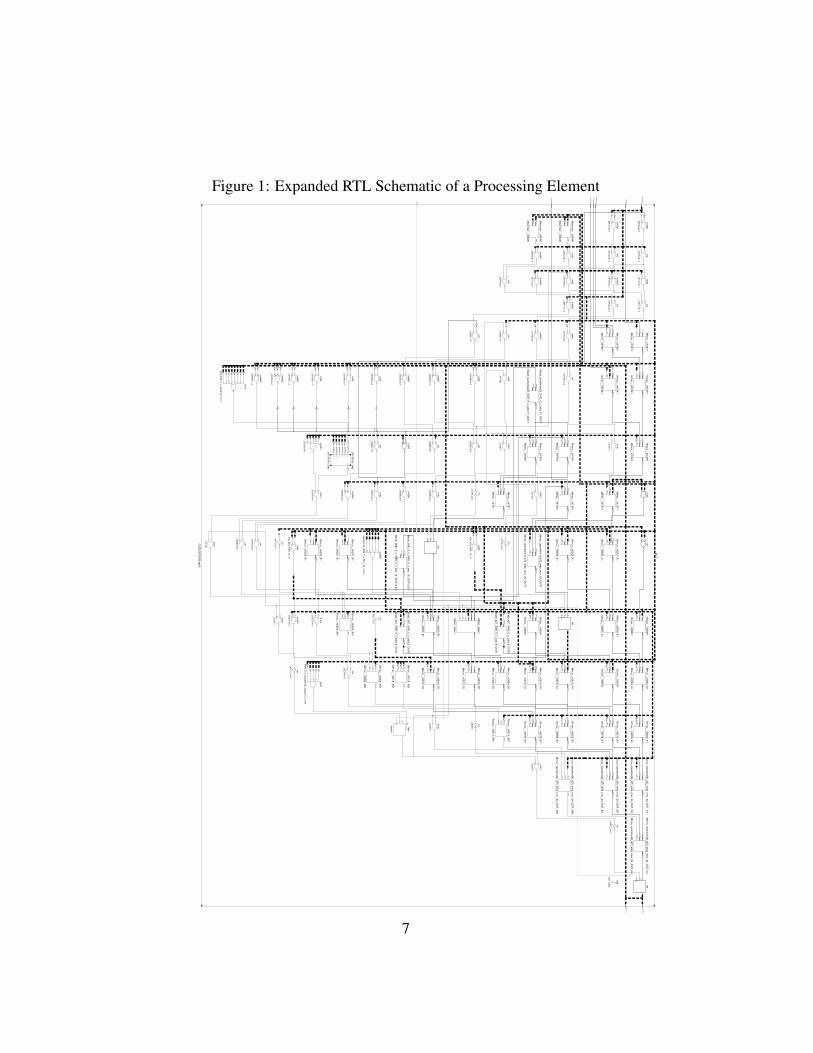
Figure 1: Expanded RTL Schematic of a Processing Elementa
nd
2b
1
_n0
15
9<
2>
1
I0 I1
O
an
d2
b1
_n0
14
1<
2>
1
I0 I1
O
Mco
mp
ar_
_n0
244
1
Mco
mp
ar_
_n0
244
1
DataA
(7:0
)
Da
taB
(7:0
)
ALE
B
Mco
mp
ar_
_n0
243
1
Mco
mp
ar_
_n0
243
1
DataA
(7:0
)
Da
taB
(7:0
)
ALE
B
or2
_n
01
60
<2
>1
I0 I1
O
or2
_n
01
42
<2
>1
I0 I1
O
an
d2
_n
02
47
<0
>1
I0 I1
O
an
d2
b1
_n
02
46
<0
>1
I0 I1
O
an
d2
_n
01
70
<3
>1
I0 I1
O
an
d2
b1
_n
01
69
<3
>1
I0 I1
O
an
d2
_n
01
52
<3
>1
I0 I1
O
an
d2
b1
_n
01
51
<3
>1
I0 I1
O
or2
_n
02
48
<0
>1
I0 I1
O
or2
_n
01
71
<3
>1
I0 I1
O
or2
_n
01
53
<3
>1
I0 I1
O
and
2b
1
_n
02
51
<1
>1
I0 I1
O
Mm
ux_
_n
012
11
Mm
ux_
_n
012
11
Da
ta0(7
:0)
Da
ta1(7
:0)
Se
l(0)
Re
sult(7:0
)
Mm
ux_
_n
01
22
1
Mm
ux_
_n
01
22
1
Da
ta0(7
:0)
Da
ta1(7
:0)
Se
l(0)
Re
sult(7:0
)
an
d2
_n
01
74
<4
>1
I0 I1
O
an
d2
b1
_n
01
73
<4
>1
I0 I1
O
or2
_n
02
60
<1
>1
I0 I1
O
or2
_n
02
53
<1
>1
I0 I1
O
Mm
ux_
_n0
123
1
Mm
ux_
_n0
123
1
Da
ta0
(7:0
)
Da
ta1
(7:0
)
Se
l(0)
Re
sult(7:0)
Mm
ux_
_n0
124
1
Mm
ux_
_n0
124
1
Da
ta0
(7:0
)
Da
ta1
(7:0
)
Se
l(0)
Re
sult(7:0)
or2
_n
01
75
<4
>1
I0 I1
O
Ma
dd
_sta
ckin
de
x[3]_
GN
D_
5_o
_ad
d_
17
_O
UT
1
Ma
dd
_sta
ckin
de
x[3]_
GN
D_
5_o
_ad
d_
17
_O
UT
1
Data
A(3
:0)
Da
taB
(3:0
)
Re
sult(3
:0)
and
2
_n
01
961
I0 I1
O
and
2
_n
01
49
<2
>1
I0 I1
O
an
d2
b1
_n
02
64
<2
>1
I0 I1
O
an
d2
b1
_n
02
55
<2
>1
I0 I1
O
and
2
_n
01
93
<4
>1
I0 I1
O
and
2
_n
01
90
<3
>1
I0 I1
O
and
2
_n
01
38
<1
>1
I0 I1
O
an
d2
b1
_n
01
56
<1
>1
I0 I1
O
an
d3
b2
_n
02
37
<0
>1
I0 I1
I2
O
an
d2
b2
_n
02
24
<1
>1
I0 I1
O
no
r8
a[7
]_G
ND
_5
_o
_e
qu
al_
24
_o
<7
>1
I0
I1 I2 I3 I4 I5 I6
I7
O
Mm
ux__
n01
26
1
Mm
ux__
n01
26
1
Da
ta0(7:0
)
Da
ta1(7:0
)
Sel(0)
Res
ult(7
:0)
an
d2
_n
01
77
1
I0 I1
O
Mm
ux__
n01
79
1
Mm
ux__
n01
79
1
Da
ta0(3:0
)
Da
ta1(3:0
)
Sel(0)
Res
ult(3
:0)
Mm
ux__
n01
80
1
Mm
ux__
n01
80
1
Da
ta0(3:0
)
Da
ta1(3:0
)
Sel(0)
Res
ult(3
:0)
or2
b1
_n
01
97
1
I0 I1
O
or2
_n
02
66
<2
>1
I0 I1
O
or2
_n
02
56
<2
>1
I0 I1
O
or2
b1
I0 I1
O
or2
_n
02
26
<1
>1
I0 I1
O_n0
113<
0>
_im
p
_n0
113<
0>
_im
p
a(7
)_G
ND
_5_
o_e
qu
al_
24_
o
ope
ration
(0)
ope
ration
(1)
ope
ration
(2)
ope
ration
(3)
ope
ration
(4)
_n
0113
an
d5
b1
_n
01
05
<4
>1
I0 I1 I2 I3
I4
O
an
d2
I0 I1
O
Mm
ux_
_n0
12
71
Mm
ux_
_n0
12
71
Da
ta0
(7:0
)
Da
ta1
(7:0
)
Se
l(0)
Re
sult(7
:0)
Mm
ux_
_n0
13
41
Mm
ux_
_n0
13
41
Da
ta0
(7:0
)
Da
ta1
(7:0
)
Se
l(0)
Re
sult(7
:0)
or2
b1
_n
01
78
1
I0 I1
O
Mm
ux_
_n0
1811
Mm
ux_
_n0
1811
Da
ta0
(3:0
)
Da
ta1
(3:0
)
Se
l(0)
Re
sult(3
:0)
inv
_n
01
97
_in
v1
IO
an
d2
_n
02
69
<3
>1
I0 I1
O
an
d2
b1
_n
02
68
<3
>1
I0 I1
O
an
d2
_n
02
41
<3
>1
I0 I1
O
an
d3
b2
_n
02
40
<2
>1
I0 I1
I2
O
or2
b1
_n
011
4<
4>
1
I0 I1
O
or2
I0 I1
O
Mm
ux_
_n0
201
_A
1
Mm
ux_
_n0
201
_A
1
Da
ta0
(7:0
)
Da
ta1
(7:0
)
Se
l(0)
Re
sult(7:0
)
Mm
ux_
_n0
202
_A
1
Mm
ux_
_n0
202
_A
1
Da
ta0
(7:0
)
Da
ta1
(7:0
)
Se
l(0)
Re
sult(7:0
)
Mm
ux_
op
era
tion
[4]_
b[7
]_w
ide
_m
ux_2
5_O
UT
1
Mm
ux_
op
era
tion
[4]_
b[7
]_w
ide
_m
ux_2
5_O
UT
1
Da
ta0
(7:0
)
Da
ta1
(7:0
)
Se
l(0)
Re
sult(7:0)
inv
_n
01
78
_in
v1
IO
an
d2
a[0
]_a
[7]_
AN
D_
10
_o
1
I0 I1
O
fde
C
CE D
Q
Msub
_G
ND
_5
_o_
GN
D_
5_
o_sub
_19
_O
UT
<3
:0>
1
Msub
_G
ND
_5
_o_
GN
D_
5_
o_sub
_19
_O
UT
<3
:0>
1
Data
A(3
:0)
Da
taB
(3:0
)
Re
sult(3
:0)
and
5b
2
op
era
tion
[4]_
GN
D_
5_
o_
Mu
x_
28_
o<
4>
1
I0 I1 I2 I3
I4
O
Mm
ux_
_n0
201
_B
1
Mm
ux_
_n0
201
_B
1
Da
ta0
(7:0
)
Da
ta1
(7:0
)
Se
l(0)
Re
sult(7:0
)
Mm
ux_
_n0
202
_B
1
Mm
ux_
_n0
202
_B
1
Da
ta0
(7:0
)
Da
ta1
(7:0
)
Se
l(0)
Re
sult(7:0
)
an
d2
b[0
]_b
[7]_
AN
D_
11_
o1
I0 I1
O
inv
_n
01
37
<1
>1
IO
or2
_n
02
70
<3
>1
I0 I1
O
or2
_n
02
42
<3
>1
I0 I1
O
an
d2
_n
011
61
I0 I1
O
Mm
ux__
n02
001
Mm
ux__
n02
001
Data
0(7
:0)
Data
1(7
:0)
Se
l(0)
Re
su
lt(7:0
)
Mm
ux_
_n
02
03_
A1
Mm
ux_
_n
02
03_
A1
Data
0(7
:0)
Data
1(7
:0)
Se
l(0)
Re
su
lt(7:0
)
fde
C
CE D
Q
Mm
ux__
n02
061
Mm
ux__
n02
061
Data
0(7
:0)
Data
1(7
:0)
Se
l(0)
Re
su
lt(7:0
)
Mad
d_a
[7]_
GN
D_
5_
o_
add
_8_
OU
T1
Mad
d_a
[7]_
GN
D_
5_
o_
add
_8_
OU
T1
Da
taA
(6:0
)
Da
taB(6
:0)
Re
sult(6:0
)
Mra
m_sta
ck1
Mra
m_sta
ck1
add
rA(3
:0)
ad
drB
(3:0
)
diA
(7:0
)
clkA
en
A
we
A
do
B(7:0
)
Mm
ux_
_n
02
03_
B1
Mm
ux_
_n
02
03_
B1
Data
0(7
:0)
Data
1(7
:0)
Se
l(0)
Re
su
lt(7:0
)
Mad
d_b
[7]_
GN
D_
5_
o_
add
_9_
OU
T1
Mad
d_b
[7]_
GN
D_
5_
o_
add
_9_
OU
T1
Da
taA
(6:0
)
Da
taB(6
:0)
Re
sult(6:0
)
vcc
XS
T_
VC
C
P
Mm
ux_
_n
020
4_
AS
1
Mm
ux_
_n
020
4_
AS
1
Se
l(0)
Da
ta0
Da
ta1
Re
sult
an
d2
_n0
27
3<
4>
1
I0 I1
O
an
d2
b1
_n0
27
2<
4>
1
I0 I1
O
or2
b1
_n
011
71
I0 I1
O
Mm
ux__
n02
04_
A1
Mm
ux__
n02
04_
A1
Data
0(7
:0)
Data
1(7
:0)
Se
l(0)
Re
su
lt(7:0
)
Mm
ux__
n02
071
Mm
ux__
n02
071
Data
0(7
:0)
Data
1(7
:0)
Se
l(0)
Re
su
lt(7:0
)
Mm
ux__
n02
12_
A1
Mm
ux__
n02
12_
A1
Data
0(7
:0)
Data
1(7
:0)
Se
l(0)
Re
su
lt(7:0
)
Mm
ux__
n02
18_
A1
Mm
ux__
n02
18_
A1
Data
0(7
:0)
Data
1(7
:0)
Se
l(0)
Re
su
lt(7:0
)
Mm
ux__
n02
04_
B1
Mm
ux__
n02
04_
B1
Data
0(7
:0)
Data
1(7
:0)
Se
l(0)
Re
su
lt(7:0
)
Mm
ux__
n02
12_
B1
Mm
ux__
n02
12_
B1
Data
0(7
:0)
Data
1(7
:0)
Se
l(0)
Re
su
lt(7:0
)
Mm
ux__
n02
18_
B1
Mm
ux__
n02
18_
B1
Data
0(7
:0)
Data
1(7
:0)
Se
l(0)
Re
su
lt(7:0
)
Mm
ux_
_n
021
8_
AS
1
Mm
ux_
_n
021
8_
AS
1
Se
l(0)
Da
ta0
Da
ta1
Re
sult
Mm
ux_
_n
020
9_
AS
1
Mm
ux_
_n
020
9_
AS
1
Se
l(0)
Da
ta0
Da
ta1
Re
sult
or2
_n
02
74
<4
>1
I0 I1
O
an
d5
PW
R_
5_
o_
op
era
tion
[4]_
eq
ua
l_3
7_
o<
4>
1
I0
I1 I2 I3
I4
O
inv
_n
011
7_
inv1
IO
Mm
ux__
n02
09
_A
1
Mm
ux__
n02
09
_A
1
Da
ta0(7:0
)
Da
ta1(7:0
)
Sel(0
)
Res
ult(7
:0)
Mm
ux__
n02
19
_A
1
Mm
ux__
n02
19
_A
1
Da
ta0(7:0
)
Da
ta1(7:0
)
Sel(0
)
Res
ult(7
:0)
Mm
ux__
n02
09
_B
1
Mm
ux__
n02
09
_B
1
Da
ta0(7:0
)
Da
ta1(7:0
)
Sel(0
)
Res
ult(7
:0)
Mm
ux__
n02
19
_B
1
Mm
ux__
n02
19
_B
1
Da
ta0(7:0
)
Da
ta1(7:0
)
Sel(0
)
Res
ult(7
:0)
Mm
ux_
_n0
219
_A
S1
Mm
ux_
_n0
219
_A
S1
Se
l(0)
Da
ta0
Da
ta1
Res
ult
inv
_n
03
25
1
IO
an
d2
_n
02
76
1
I0 I1
O
fdp
e
en
ab
le
C
CE D
PR
E
Q
Mm
ux_
ope
ratio
n[4
]_a
[7]_
wid
e_m
ux_
24_
OU
T_A
1
Mm
ux_
ope
ratio
n[4
]_a
[7]_
wid
e_m
ux_
24_
OU
T_A
1
Da
ta0(7:0)
Da
ta1(7:0)
Sel(0)
Re
sult(7
:0)
Mm
ux_
ope
ratio
n[4
]_a
[7]_
wid
e_m
ux_
24_
OU
T_B
1
Mm
ux_
ope
ratio
n[4
]_a
[7]_
wid
e_m
ux_
24_
OU
T_B
1
Da
ta0(7:0)
Da
ta1(7:0)
Sel(0)
Re
sult(7
:0)
Mm
ux_o
pera
tion
[4]_
a[7
]_w
ide
_m
ux_
24_
OU
T_A
S1
Mm
ux_o
pera
tion
[4]_
a[7
]_w
ide
_m
ux_
24_
OU
T_A
S1
Sel(0)
Data
0
Data
1
Re
sult
or2
b1
_n
02
77
1
I0 I1
O
Mm
ux_
op
era
tion
[4]_
a[7
]_w
ide_
mux_
24
_O
UT
_rs
1
Mm
ux_
op
era
tion
[4]_
a[7
]_w
ide_
mux_
24
_O
UT
_rs
1
Da
taA(7:0
)
Da
taB
(7:0)
Ad
dS
ub
Res
ult(7
:0)
inv
_n
02
77
_in
v1
IO
fde
C
CE D
Q
gn
d
XS
T_
GN
D
G
pu:1
G1[7
].G2[7
].RB
.ap
u0
in_
do
wn
(7:0
)
in_
left(7
:0)
in_
loa
d(7
:0)
in_
righ
t(7:0
)
in_u
p(7
:0)
opera
tion
(4:0
)
clk
ou
tpu
t(7:0
)
ou
t_lo
ad(7
:0)
7

consume once synthesised, creating a key design trade-off that is explored in latersections. The implemented operations are shown in Table 1 on page 10.
2.1.2 Internal Signals
Accumulator A (8 bits): The accumulator stores the result of arithmetical andlogical operations.
Register B (8 bits): Register B is used to provide an additional operand forarithmetic and logical operations. This is also where values from neighbouringprocessing elements are initially loaded.
Stack (16x8bits): The stack gives FILO storage that can be expanded to occupythe total distributed RAM allocated to each CLB. The precise allocation of thisstorage differs for each FPGA model, with the XC6SLX45 having 16x8-bit, dual-port distributed RAM blocks. It is also possible to force this storage to the FPGA’sshared block RAM, or even to external DDR, if additional storage is required. Itis possible to push values to the shared stack from A or B, and pop values fromthe stack to A or B.
Enable Bit: For a significant number of image processing tasks, every pro-cessing element is concurrently performing an identical operation. For the caseswhere this is not appropriate, an enable bit is included. In the current implement-ation, this signal is internal to the PE itself, and is set according to the value ofaccumulator A, via the Zero Flag. There is a single instruction to re-enable allPEs, ensuring a known configuration, once other tasks have been previously per-formed.
Zero Flag The zero flag is set when the value of accumulator A is zero. It isthen possible to use this flag to selectively disable PEs.
8

2.1.3 Choice of Instruction Set
Due to the nature of FPGAs, there is a fundamental design compromise requiredbetween the complexity of each processing element, and the number of elementsthat are used in a given grid (which determines the resolution). The complexity(FPGA area) of each element corresponds to the number and complexity of op-erations it is required to perform [25]. FPGAs of a given series will come in arange of models, with a differing number and distribution of logic blocks. The in-struction that requires the greatest number of cascaded logic changes is the factordetermining the speed at which the system as a whole can operate. For example,an instruction to find the median of the current PE’s value, and that of the thePEs directly adjacent to it would require a greater number of logic stages thanany other instruction described. While such an instruction would be a significantadvantage when median filtering (section 3.3.2) is required, its inclusion would beof significant detriment to the system’s general purpose performance. For certainscenarios this trade-off is acceptable, particularly if the final application of thesystem is known in detail. It is also possible to avoid this trade-off, with somesystems taking advantage of the reconfigurable nature of FPGAs by dynamicallyreconfiguring the deployed system to accomplish a specific task [11, 12, 26]. Forthe purposes of this image processing system, the performance of general instruc-tions has been prioritised over performance at specific tasks.
2.2 The Processing Array
Many common image processing tasks are particularly localised, operating on ad-jacent groups of pixels, while generally having minimal input from pixels that arefurther away. Under this massively parallel architecture, a Processing Array iscreated, consisting of a large number of linked Processing Elements (PEs). EachPE is connected to its immediate cardinal neighbours (that is, to the PEs above,below, and to the left and right). These connections enable the simple implement-ation of many common image processing processes. There are also additional
9

Table 1: Processing Element Instruction ListOpCode Instruction Description Dataflow
0 NOP No operation -1 CopyBA Copy from B to A a( b2 CopyAB Copy from A to B b( a3 OrBA Bitwise OR a( a or b4 AndBA Bitwise AND a( a and b5 XorBA Bitwise XOR a( a � b6 SumBA Add B to A a( a+b7 SubBA Subtract B from A a( a � b8 AbsA Absolute Value of A a( |a|9 ClrA Clear A a( 010 ClrB Clear B b( 011 LdUp Load from PE above into B b( above.a12 LdDown Load from PE below into B b( below.a13 LdLeft Load from PE to the left into B b( left.a14 LdRight Load from PE to the right into B b( right.a15 Load Load from Previous PE into B b( prev.a16 Swap Swap values of A and B b, a17 DblA Double the value of A a( a ⇥ 218 HalveA Halve the value of A a( a ÷ 219 MaxAB Return maximum of A and B a( max (a, b)20 MinAB Return minimum of A and B a( min (a, b)21 PushA Push value of A to stack Stack( a22 PopA Pop value of A from stack a( Stack23 PushB Push value of B to stack Stack( b24 PopA Pop value of B from stack b( Stack25 IncA Increment A a( a+126 DecA Decrement A a( a�127 DisableZ Disable PEs with a=0 -28 EnableAll Enable all PEs (default) -
10
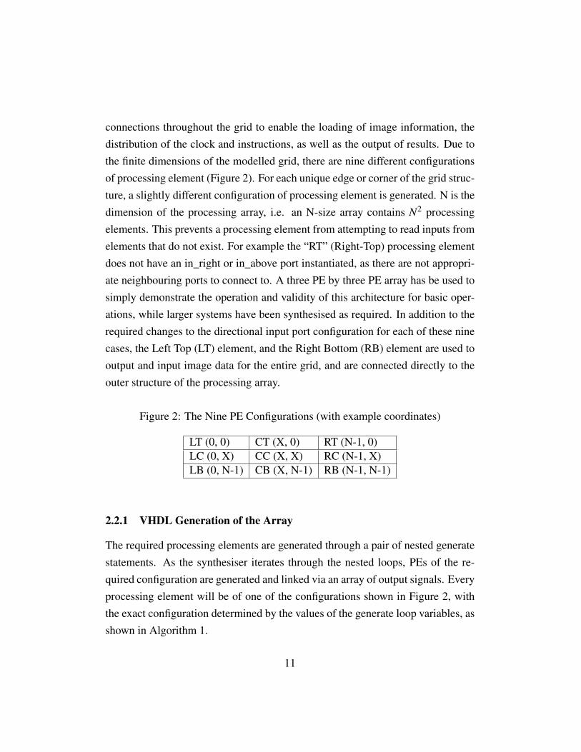
connections throughout the grid to enable the loading of image information, thedistribution of the clock and instructions, as well as the output of results. Due tothe finite dimensions of the modelled grid, there are nine different configurationsof processing element (Figure 2). For each unique edge or corner of the grid struc-ture, a slightly different configuration of processing element is generated. N is thedimension of the processing array, i.e. an N-size array contains N2 processingelements. This prevents a processing element from attempting to read inputs fromelements that do not exist. For example the “RT” (Right-Top) processing elementdoes not have an in_right or in_above port instantiated, as there are not appropri-ate neighbouring ports to connect to. A three PE by three PE array has be used tosimply demonstrate the operation and validity of this architecture for basic oper-ations, while larger systems have been synthesised as required. In addition to therequired changes to the directional input port configuration for each of these ninecases, the Left Top (LT) element, and the Right Bottom (RB) element are used tooutput and input image data for the entire grid, and are connected directly to theouter structure of the processing array.
Figure 2: The Nine PE Configurations (with example coordinates)
LT (0, 0) CT (X, 0) RT (N-1, 0)LC (0, X) CC (X, X) RC (N-1, X)LB (0, N-1) CB (X, N-1) RB (N-1, N-1)
2.2.1 VHDL Generation of the Array
The required processing elements are generated through a pair of nested generatestatements. As the synthesiser iterates through the nested loops, PEs of the re-quired configuration are generated and linked via an array of output signals. Everyprocessing element will be of one of the configurations shown in Figure 2, withthe exact configuration determined by the values of the generate loop variables, asshown in Algorithm 1.
11

Algorithm 1 Generation of Processing Elements
G1 : f o r i in N�1 downto 0 g e n e r a t e��In X d i r e c t i o nG2 : f o r j in N�1 downto 0 g e n e r a t e��In Y d i r e c t i o n
��T h i s example shows one o f t h e n i n e c o n f i g u r a t i o n s .
LT : i f ( ( i =0) and ( j = 0 ) ) g e n e r a t e��Genera te L e f t Top u n i t .apu0 : pu port map (o p e r a t i o n => g I n s t r u c t i o n , ��Same f o r a l l PEsc l k => c lk ,dummy=>gDummy(N⇤ j + i ) ,o u t p u t => dou t ( i , j ) ��Read by a d j a c e n t u n i t s .
in_down=> dou t ( i , j + 1 ) , ��Only two d i r e c t i o n a l c o n n e c t i o n s .i n _ r i g h t => dou t ( i +1 , j ) ,
i n _ l o a d => dou t ( i +1 , j ) , ��For l o a d i n g da tao u t _ l o a d =>gOut , ��Unique t o LT) ;
end g e n e r a t e LT ;
��S i m i l a r f o r o t h e r e i g h t c a s e s
end g e n e r a t e G2 ;end g e n e r a t e G1 ;
12

The result of this synthesis can be seen in Figure 3. The processing array levelports of gLoad, gOut, gInstruction and clk can be seen along the outer region ofthe schematic, connecting to the internal ports, as described in the relevant portmap (Algorithm 1) . In this case the processing array has been implemented asa square grid of n processing elements in each direction. This means that thetotal array contains n2 elements. While this initial implementation is a square,this is not a particular requirement, and only minimal changes need to be madeto the generate loops (the addition of a new variable for the range checking in they-direction).
13

Figure 3: Unexpanded Schematic of a 2x2 Processing Arraypu
G1[1
].G2[1
].RB
.apu0
in_d
ow
n(7
:0)
in_le
ft(7:0
)
in_lo
ad
(7:0
)
in_rig
ht(7
:0)
in_u
p(7
:0)
op
era
tion
(4:0
)
clk
ou
tpu
t(7:0
)
ou
t_lo
ad
(7:0
)
pu
G1[0
].G2[1
].LB
.apu0
in_d
ow
n(7
:0)
in_le
ft(7:0
)
in_lo
ad
(7:0
)
in_rig
ht(7
:0)
in_u
p(7
:0)
op
era
tion
(4:0
)
clk
ou
tpu
t(7:0
)
ou
t_lo
ad
(7:0
)
pu
G1[1
].G2[0
].RT.a
pu0
in_d
ow
n(7
:0)
in_le
ft(7:0
)
in_lo
ad
(7:0
)
in_rig
ht(7
:0)
in_u
p(7
:0)
op
era
tion
(4:0
)
clk
ou
tpu
t(7:0
)
ou
t_lo
ad
(7:0
)
gn
d
XS
T_
GN
D
G
pu
G1[0
].G2[0
].LT.a
pu0
in_d
ow
n(7
:0)
in_le
ft(7:0
)
in_lo
ad
(7:0
)
in_rig
ht(7
:0)
in_u
p(7
:0)
op
era
tion
(4:0
)
clk
ou
tpu
t(7:0
)
ou
t_lo
ad
(7:0
)
PA
:1
PA
gIn
structio
n(4
:0)
gLoad
(7:0
)
clk
gD
um
my(3
:0)
gO
ut(7
:0)
14

3 Exploration of Image Processing Tasks
The implementation of a number of general image processing tasks demonstratesthe use of the massively parallel processing array architecture. These are intendedto demonstrate a broad range of general imaging requirements. In some cases,the inclusion of more specialised instructions has the potential to substantiallysimplify or accelerate the performance of specific tasks. In these scenarios, thepotential changes are explored. However, the priority remains on general purposeperformance. The simulation of these tasks was performed by Xilinx ISim (ISESimulator).
3.1 Loading the Processing Array
The current configuration of the general purpose image processing architecture isbased upon receiving a single serial stream of pixel information, which is thendistributed through the processing array. The input value stream is connected tothe final processing element, at the bottom right of the processing array. Eachsuccessive value is loaded into register B via the in_load port, then copied toregister A. This value will then be read by the next processing element, on thefollowing cycle.
Algorithm 2 Loading the Processing Array
��Loading t h e Arrayf o r i in 0 to N⇤N�1 loop
gLoad <= I n p u t S i g n a l ( i ) ;g I n s t r u c t i o n <= Load ;
wait f o r c l k _ p e r i o d ;g I n s t r u c t i o n <= CopyBA ;
wait f o r c l k _ p e r i o d ;end loop ;
When this procedure is applied using test values from 1 through 9, the opera-
15

tion of the array is clear. The first input value must travel through the entire arraybefore reaching the top-left position. The simulation output (Figure 7) shows abehavioural simulation of this same example. Once the value of the top-left pro-cessing element has been set, the entire processing array has been propagated withvalues. At this point, the required image processing can be performed.
Figure 4: After First Step
- - -- - -- - 1
Figure 5: After Fifth Step
- - -- 1 23 4 5
Figure 6: The Final Result
1 2 34 5 67 8 9
This loading procedure requires two clock cycles per individual processingelement, due to the completely serial nature of this method of image loading, thetime taken linearly increases with the number of pixels. To give approximateperformance requirements, Table 2 shows the portion of total clock cycles thatare required for the loading operation. The transfer of the processed image data
16

Figu
re7:
Sim
ulat
ion
ofLo
adO
pera
tion
17
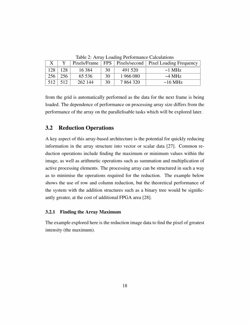
Table 2: Array Loading Performance CalculationsX Y Pixels/Frame FPS Pixels/second Pixel Loading Frequency
128 128 16 384 30 491 520 ~1 MHz256 256 65 536 30 1 966 080 ~4 MHz512 512 262 144 30 7 864 320 ~16 MHz
from the grid is automatically performed as the data for the next frame is beingloaded. The dependence of performance on processing array size differs from theperformance of the array on the parallelisable tasks which will be explored later.
3.2 Reduction Operations
A key aspect of this array-based architecture is the potential for quickly reducinginformation in the array structure into vector or scalar data [27]. Common re-duction operations include finding the maximum or minimum values within theimage, as well as arithmetic operations such as summation and multiplication ofactive processing elements. The processing array can be structured in such a wayas to minimise the operations required for the reduction. The example belowshows the use of row and column reduction, but the theoretical performance ofthe system with the addition structures such as a binary tree would be signific-antly greater, at the cost of additional FPGA area [28].
3.2.1 Finding the Array Maximum
The example explored here is the reduction image data to find the pixel of greatestintensity (the maximum).
18

Algorithm 3 Reduction to find Maximum
��To f i n d t h e maximum v a l u e f o r each Columnf o r i in 0 to (N�1) loop
g I n s t r u c t i o n <= LdDownwait f o r c l k _ p e r i o d ;
g I n s t r u c t i o n <= MaxAB;wait f o r c l k _ p e r i o d ;
end loop ;
��To f i n d maximum f o r each Rowf o r i in 0 to (N�1) loop
g I n s t r u c t i o n <= LdRightwait f o r c l k _ p e r i o d ;
g I n s t r u c t i o n <= MaxAB;wait f o r c l k _ p e r i o d ;
end loop ;
There are two stages involved in performing a complete minimum or max-imum reduction. In the first stage the maximum value in each column is found,and this becomes the value for every PE in each column (Figure 9). This is per-formed by each PE loading the value of the PE below it, then on the next clockcycle, keeping the higher of its own value, or the value from below. This pro-cedure is then repeated N-1 times, sufficient for correct operation in the worstcase, when the maximum value is in the bottom row. The maximum value in eachrow can be found similarly, again with the operation performed N-1 times. If thecolumn reduction operation has already been performed, every PE now containsthe maximum value that was found in the array (Figure 10), which can then easilybe read from the output port on the first element (LT).
19

Figure 8: Initial Values for Reduction (Finding the Maximum)
0 1 23 4 56 7 8
Figure 9: All Column Maximums Found
6 7 86" 7" 8"6" 7" 8"
Figure 10: Then Row Maximums Found
8 8 88 8 88 8 8
The separation of row and column reduction thus enables the completion ofthese operations in O(n) time.
3.3 Simple Image Filtering
3.3.1 Mean Filtering
When performing image processing tasks such as edge detection or disparity map-ping, pre-filtering is used to increase accuracy. Due to the nature of this imageprocessing architecture, it is simple to perform a four-way “fast” mean filter, re-placing each pixel with the mean of its cardinal neighbours (Figure 11). Theoperation of such a filter on a small array is shown in Figure 13. Note that the
20

values of the edge elements are not useful, as their means include values that arebeyond the edge of the processing array. This loss of edge pixels is common inimage processing algorithms.
Figure 11: Mask for Four-way Mean Operation
1/41/4 1/4
1/4
Figure 12: Initial Array Values
5 5 4 66 6 4 57 30 6 45 7 3 6
Figure 13: Following Four-way Mean Operation
- - - -- 11 5 -- 7 10 -- - - -
It can be seen that the outlier of “30” has been removed. However, while theoutlier itself has been filtered away, it has still had a substantial impact on two ofthe remaining image pixels, illustrating a key downside of mean-based filtering,and other linear filtering schemes. The choice of which mean window to use is acompromise between retaining image sharpness, and the noise reduction require-ments, with too large a window creating a “blur” effect. For the processing array
21

implementation, the mean filtering is performed by loading the four neighbouringpixels into the stack, then popping them back in turn. To avoid overflowing duringthe interim state, each operand is divided by four before it is summed. The centralpixel now contains the four-way mean of the adjacent pixels.
3.3.2 Median Filtering
The non-linear technique of median filtering is commonly used as a pre-filteringstage, as it does not suffer from the aforementioned disadvantages of mean-basedapproaches[10]. The structure of FPGAs lends itself to the application of “fast-median” algorithms, which generally give reasonable approximations of the truemedian, while being much simpler to implement. The standard 3x3 fast medianis executed by first finding the median of each column, and then finding the me-dian of these results. This approach is used in specialised median filtering stages[29], but proved to be too computationally expensive for this massively parallelimplementation. For this reason, the median filtering operations shown in al-gorithm 5 have not been implemented on the PEs. This is because the synthesis ofmedian-specific instructions to allow either vertical and horizontal medians to becalculated in a single instruction requires the use additional logic levels. This issignificantly greater than the logic required for any other single instruction, settinga maximum clock speed that can be reached by the system. This means that theaddition of these instructions significantly degrades performance for other imageprocessing tasks.
22

Algorithm 4 Fast Median Filtering with a 3x3 window (using specialised instruc-tions)
��F i n d i n g V e r t i c a l Medians
g I n s t r u c t i o n <=MedianUD ; ��Load V e r t i c a l Median i n t o Bwait f o r c l k _ p e r i o d ;
g I n s t r u c t i o n <=CopyBA ; ��Copy B i n t o Await f o r c l k _ p e r i o d ;
��F i n d i n g H o r i z o n t a l Mediansg I n s t r u c t i o n <=MedianLR ; ��Load H o r i z o n t a l Median i n t o B
wait f o r c l k _ p e r i o d ;g I n s t r u c t i o n <=CopyBA ; ��Copy B i n t o A
wait f o r c l k _ p e r i o d ;
23
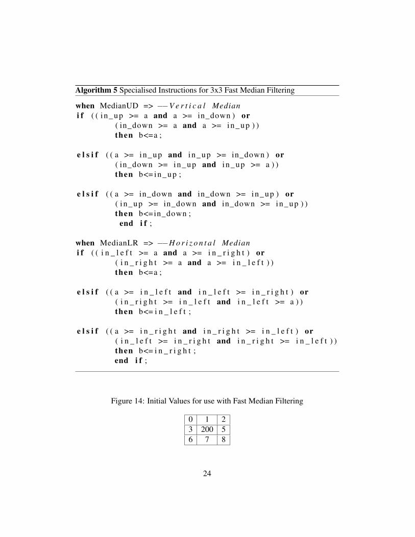
Algorithm 5 Specialised Instructions for 3x3 Fast Median Filtering
when MedianUD => ��V e r t i c a l Mediani f ( ( i n_up >= a and a >= in_down ) or
( in_down >= a and a >= in_up ) )then b<=a ;
e l s i f ( ( a >= in_up and i n_up >= in_down ) or( in_down >= in_up and i n_up >= a ) )then b<= in_up ;
e l s i f ( ( a >= in_down and in_down >= in_up ) or( in_up >= in_down and in_down >= in_up ) )then b<=in_down ;
end i f ;
when MedianLR => ��H o r i z o n t a l Mediani f ( ( i n _ l e f t >= a and a >= i n _ r i g h t ) or
( i n _ r i g h t >= a and a >= i n _ l e f t ) )then b<=a ;
e l s i f ( ( a >= i n _ l e f t and i n _ l e f t >= i n _ r i g h t ) or( i n _ r i g h t >= i n _ l e f t and i n _ l e f t >= a ) )then b<= i n _ l e f t ;
e l s i f ( ( a >= i n _ r i g h t and i n _ r i g h t >= i n _ l e f t ) or( i n _ l e f t >= i n _ r i g h t and i n _ r i g h t >= i n _ l e f t ) )then b<= i n _ r i g h t ;end i f ;
Figure 14: Initial Values for use with Fast Median Filtering
0 1 23 200 56 7 8
24

Figure 15: All Column Medians Found
# # #3 7 5" " "
Figure 16: Then Row Medians Found
- - -! 5 - - -
3.3.3 Sobel Operator
The Sobel operator is used as an edge detection algorithm, finding gradients inthe x and y directions. Using the separability of the Sobel operator (Figure 18),this operation can be easily performed in a highly parallel way. The separatedmatrices are known as the smoothing and difference operators [30]. Sobel-basededge detection is an area that FPGAs can perform very well in, due to the largenumber of simple operations that are required [31].
Figure 17: Mask for Sobel Operator (x-direction)
-1 1-2 2-1 1
This separability allows the component gradients to be determined by separaterow and column operations, a good match for the massively parallel processingarray. The application of the Sobel operator in the x-direction will be used to
25

Figure 18: Separability of Sobel Operator (x-direction) [27]0
@�1 0 1�2 0 2�1 0 1
1
A=
0
@121
1
A ⇧��1 0 1
�
Figure 19: Initial Array Values for Sobel
0 1 2 38 10 12 78 9 10 1112 13 14 15
demonstrate this process. After a set of image data has been loaded into the array(Figure 19), every processing element loads the value of the PE directly above it,and pushes this value to the stack, it then loads the value of the element below itinto register B. Both of these values are loaded before any arithmetic operationstake place, so that other PEs are able to read the initial values correctly. Onceboth values are loaded, the initial pixel value in A is doubled, and the pixels fromthe two vertically adjacent elements subtracted. The result of these operations isshown in Figure 20. The row operations must then be performed. Again thestack is used to ensure that the value of A remains untouched until all loading iscomplete. For this portion of the algorithm, the outcome is that the final valueis the previous value of the left PE, minus the previous value of the right PE
Figure 20: Following Column Operations
- - - -8 10 12 0-4 -5 -6 0- - - -
26

Figure 21: Sobel Process Complete in the x-direction
- - - -- 4 -10 -- -2 5 -- - - -
(Figure 21). The instructions required to perform these operations is shown inalgorithm 6.
27

Algorithm 6 Sobel Operator in the x-direction
��S o b e l Opera tor i n X d i r e c t i o n
�� F i r s t Par t o f S o b e l i n x ( Columns )g I n s t r u c t i o n <= LdUp ;
wait f o r c l k _ p e r i o d ;g I n s t r u c t i o n <= PushB ;
wait f o r c l k _ p e r i o d ;g I n s t r u c t i o n <= LdDown ;
wait f o r c l k _ p e r i o d ;g I n s t r u c t i o n <=DblA ;
wait f o r c l k _ p e r i o d ;g I n s t r u c t i o n <=AddBA ;
wait f o r c l k _ p e r i o d ;g I n s t r u c t i o n <=PopB ;
wait f o r c l k _ p e r i o d ;g I n s t r u c t i o n <=AddBA ;
wait f o r c l k _ p e r i o d ;��Every PE = above + 2⇤ i t s e l f + below
�� Second Par t o f S o b e l i n X ( Rows )g I n s t r u c t i o n <= LdLef t ;
wait f o r c l k _ p e r i o d ;g I n s t r u c t i o n <= PushB ;
wait f o r c l k _ p e r i o d ;g I n s t r u c t i o n <= LdRight ;
wait f o r c l k _ p e r i o d ;g I n s t r u c t i o n <=CopyBA ;
wait f o r c l k _ p e r i o d ;g I n s t r u c t i o n <=PopB ;
wait f o r c l k _ p e r i o d ;g I n s t r u c t i o n <=SubBA ;
wait f o r c l k _ p e r i o d ;��Every PE = l e f t � r i g h t��S o b e l i n X d i r e c t i o n c o m p l e t e d .
28

Figure 22: Separability of Sobel Operator (y-direction)0
@1 2 10 0 0�1 �2 �1
1
A=
0
@10�1
1
A ⇧�
1 2 1�
A similar process is used to approximate image gradients in the y-directionFigure 22 . Once the gradient magnitudes are found, the edge intensity can becalculated using a polar conversion. Alternatively, an approximation of the overalledge intensity can be found by summing the absolute values of the gradients ofthe x and y direction.
3.4 Stereo Vision
The hardware required to capture stereo images can be implemented inexpens-ively. However, the computational performance required to process these imagesin a reasonable time remains prohibitive for many applications, particularly forembedded devices. For this reason the potential for FPGAs to accelerate this pro-cessing has been an area of keen development [32, 33, 9, 34]. The algorithmsdiscussed below are area-based techniques for correlating two stereo images. Instereo correspondence calculations, the algorithm compares a window (for ex-ample a 5x5 square) in one image, with every possible window in the other im-age. The relative pixel offset between a window area and its best match (greatestcorrelation) gives a value of stereo disparity. This is repeated for every window ofthe initial image, with a greater disparity indicating that the object is closer to thecameras. On a serial processor, smaller window sizes dramatically increase thetotal number of operations required, and hence time taken [32]. In conventionalstereo imaging, each image is the current output frame of calibrated left and rightcameras. For the purposes of stereo vision, calibrated cameras are those alignedalong a single horizontal plane. This calibration means that stereo correspondencecomparisons only need to be made in the x axis, significantly reducing the com-
29

putational intensity of the processes. The Sum of Absolute Differences (SAD)algorithm is a simple method for determining a correlation between two images.Under the SAD method, smaller window sizes generally give a greater level ofaccuracy. The performance of stereo vision systems can often be improved byfinding edges (via the Sobel operator or similar), and then running a correspond-ence algorithm such as SAD on the processed edges [35].
3.4.1 Sum of Absolute Differences
The instructions required to calculate the SAD are shown in 7. The pixel values ofthe left and right stereo image are subtracted (Figure 23), and the absolute valueof these differences is taken (Figure 24). This absolute value is then summedalong each three pixel column (Figure 25) and row (Figure 26). When these oper-ations are completed, each PE contains the 3x3 SAD value for that disparity. Thedisparity is then increased (shift one of the images across by one pixel), and theoperations repeated.
Figure 23: Example Left and Right Image Differences
1 4 6-1 8 92 -3 -2
Figure 24: Absolute Value of Left and Right Image Differences
1 4 61 8 92 3 2
30

Algorithm 7 Summing Absolute Differences
�� 3 x3 SAD I m p l e m e n t a t i o n�� A has l e f t image , B has r i g h t imageg I n s t r u c t i o n <= SubBA ;
wait f o r c l k _ p e r i o d ;g I n s t r u c t i o n <= AbsA ;
wait f o r c l k _ p e r i o d ;��Now have AD f o r each p i x e l p a i r .
g I n s t r u c t i o n <= LdUp ;wait f o r c l k _ p e r i o d ;
g I n s t r u c t i o n <= PushB ;wait f o r c l k _ p e r i o d ;
g I n s t r u c t i o n <= LdDown ;wait f o r c l k _ p e r i o d ;
g I n s t r u c t i o n <= AddBA ;wait f o r c l k _ p e r i o d ;
g I n s t r u c t i o n <=PopB ;wait f o r c l k _ p e r i o d ;
g I n s t r u c t i o n <= AddBA ;wait f o r c l k _ p e r i o d ;
��Now Column SAD done .
g I n s t r u c t i o n <= LdLef t ;wait f o r c l k _ p e r i o d ;
g I n s t r u c t i o n <= PushB ;wait f o r c l k _ p e r i o d ;
g I n s t r u c t i o n <= LdRight ;wait f o r c l k _ p e r i o d ;
g I n s t r u c t i o n <= AddBA ;wait f o r c l k _ p e r i o d ;
g I n s t r u c t i o n <=PopB ;wait f o r c l k _ p e r i o d ;
g I n s t r u c t i o n <= AddBA ;wait f o r c l k _ p e r i o d ;
��Sum o f AD done .��Each PU now has 3 x3 SAD f o r t h i s d i s p a r i t y .
31

Figure 25: Column SAD
# # #4 15 17" " "
Figure 26: Sum of Absolute Differences for a Single Disparity Level
- - -! 36 - - -
The inclusion of additional higher-level logic will be required to maintain thevalue of the lowest SAD, and the disparity for which this occurred. The disparitythat gave the lowest SAD will become that pixel’s value in the final disparity map.The generated disparity map then gives an indication of the relative distance ofeach image pixel from the cameras. The potential for more specialised FPGAco-processors to dramatically enhance SAD systems is already known [36, 20].
3.5 Demonstration of Conditional Activation
The current implementation of this general purpose image co-processor supportsonly one method of conditional activation. This is provided by the DisableZ op-eration, which disables all PEs that have a zero value in register A. When a PEis disabled, it does not execute any further operations until after the issue of anEnableAll command. These operations demonstrate basic conditional executionwithin the array.
32
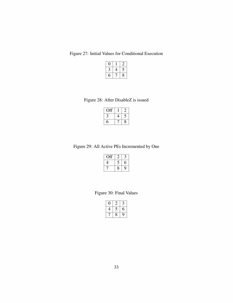
Figure 27: Initial Values for Conditional Execution
0 1 23 4 56 7 8
Figure 28: After DisableZ is issued
Off 1 23 4 56 7 8
Figure 29: All Active PEs Incremented by One
Off 2 34 5 67 8 9
Figure 30: Final Values
0 2 34 5 67 8 9
33
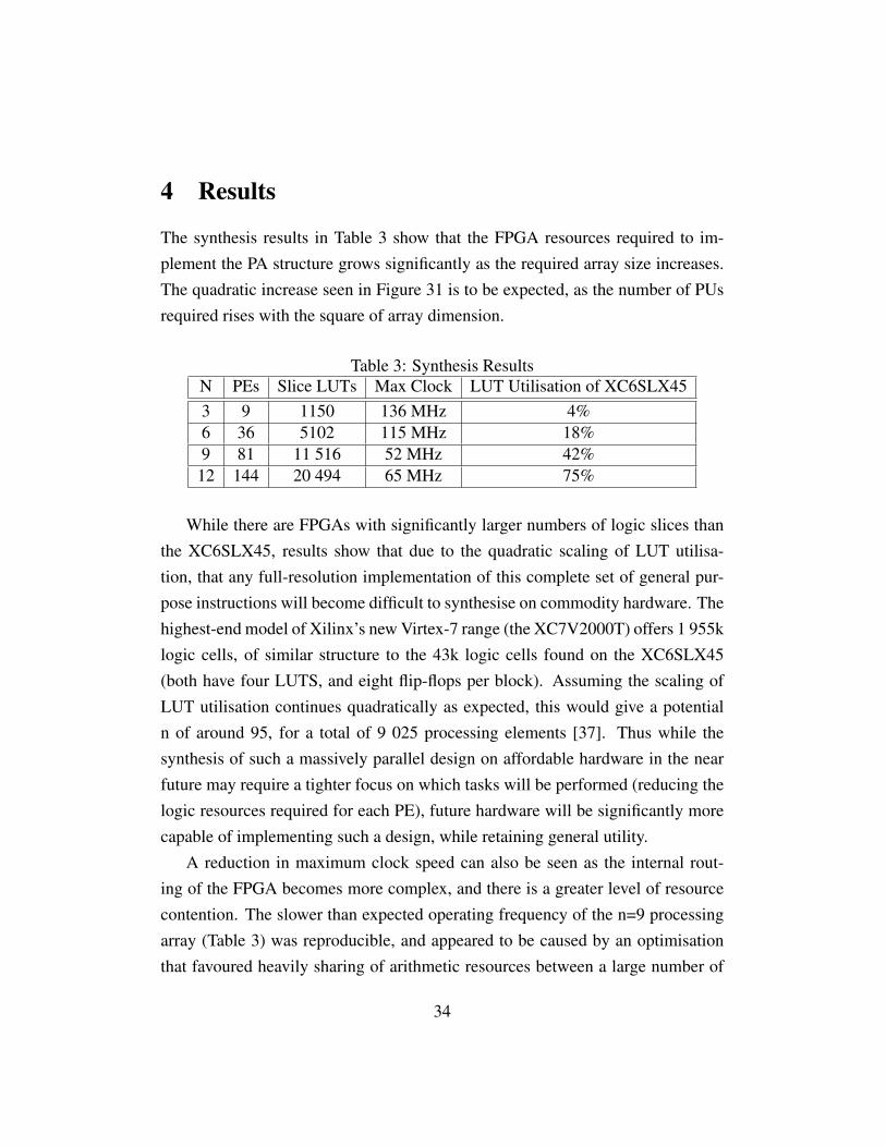
4 Results
The synthesis results in Table 3 show that the FPGA resources required to im-plement the PA structure grows significantly as the required array size increases.The quadratic increase seen in Figure 31 is to be expected, as the number of PUsrequired rises with the square of array dimension.
Table 3: Synthesis ResultsN PEs Slice LUTs Max Clock LUT Utilisation of XC6SLX453 9 1150 136 MHz 4%6 36 5102 115 MHz 18%9 81 11 516 52 MHz 42%
12 144 20 494 65 MHz 75%
While there are FPGAs with significantly larger numbers of logic slices thanthe XC6SLX45, results show that due to the quadratic scaling of LUT utilisa-tion, that any full-resolution implementation of this complete set of general pur-pose instructions will become difficult to synthesise on commodity hardware. Thehighest-end model of Xilinx’s new Virtex-7 range (the XC7V2000T) offers 1 955klogic cells, of similar structure to the 43k logic cells found on the XC6SLX45(both have four LUTS, and eight flip-flops per block). Assuming the scaling ofLUT utilisation continues quadratically as expected, this would give a potentialn of around 95, for a total of 9 025 processing elements [37]. Thus while thesynthesis of such a massively parallel design on affordable hardware in the nearfuture may require a tighter focus on which tasks will be performed (reducing thelogic resources required for each PE), future hardware will be significantly morecapable of implementing such a design, while retaining general utility.
A reduction in maximum clock speed can also be seen as the internal rout-ing of the FPGA becomes more complex, and there is a greater level of resourcecontention. The slower than expected operating frequency of the n=9 processingarray (Table 3) was reproducible, and appeared to be caused by an optimisationthat favoured heavily sharing of arithmetic resources between a large number of
34

Figure 31: LUT Utilisation following Synthesis
4%
19%
42%
75%
0%
10%
20%
30%
40%
50%
60%
70%
80%
0 2 4 6 8 10 12 14
LUT
Util
isat
ion
%
Dimension of PA (n)
Figure 32: Maximum Clock Speed
0
20
40
60
80
100
120
140
160
0 2 4 6 8 10 12 14
Max
Clo
ck R
ate
(MHz
)
Dimension of PA (n)
35

processing elements. It is possible to adjust synthesiser performance to prioritisefor logic area or clock speed, through configuring its approach to logic block shar-ing, however, this did not have a significant impact on the synthesis results. Therelatively low clock speeds that can be seen for the larger PAs would significantlyincrease the time required to load in image frames, but in many cases would notsubstantially slow the image processing itself.
36

5 Conclusion
This implemented system shows that a system consisting of a parallel processingarray, made up of a large number of interconnected PUs can achieve high levels oftheoretical image processing performance, performing many processing in a smallnumber of clock cycles. This sort of architecture would be especially effectivewhen operating on larger image sizes, as many common image processing taskscan be performed at a reduced order compared to serial processing.
With the current instruction set, commercially available FPGA hardware doesnot offer sufficient logic area to implement this generalised a parallel architectureon a realistic scale, as even relatively small processing arrays will consume theentirety of available logic resources of current FPGA hardware. Unfortunately,with current technology, there are still significant compromises that must be madeto the generalised capabilities of individual processing elements, to ensure it ispossible to implement this kind of massively parallel architecture at useful imagesizes. The chosen instruction set was relatively complex compared to other re-search approaches [24, 23], and it is possible that further simplification of the PEsabilities in favour of a greater level centralised logic would allow for improvedscaling.
37

6 Future Work
This project has demonstrated the possibility of developing a general purpose im-age processing architecture through the application of a massively-parallel gridarchitecture. In this case the architecture’s utility was benchmarked through theuse of the Xilinx iSim simulator. It is expected that future work would include thesynthesis of this design onto physical FPGA hardware, allowing the connectionof cameras and output screens. Unfortunately, current FPGA hardware does notallow for the synthesis of full-frame size processing arrays.
6.1 Hardware Implementation
Throughout its development, this architecture was synthesised for the Xilinx Spartan-6 XC6SLX45 FPGA. The configuration onto a physical device would only re-quires the addition of for input/output pin allocations [15]. It is likely that toachieve useful results on physical hardware, an FPGA model with a greater num-ber of CLBs would be required. It is possible to explore techniques such as hand-ling small sections of the image at one time. The viability of such an approachdepends on the specifics of the imaging tasks that must be performed. For ex-ample, as covered earlier, for calibrated cameras the SAD method only examineswindows along a single horizontal line, so a system than can break-down the im-age into horizontal strips could be appropriate, while other imaging tasks wouldbe most performant with square image sections. This kind of image partitioningof images thus creates its own set of design compromises. With current hardwareit is possible that a dynamically reconfigurable approach would also be useful,by creating a versatile system that can perform a variety of tasks, but requires re-configuration when moving between them. This may allow a better balance to bestruck between PE capability and PA size.
38

6.2 Camera Interfacing
The architecture in its current state has been developed based around a purelyserial image signal as the input to the processing grid. This requires the imagedata for each pixel to traverse the grid from the final PE to the appropriate element.It is likely that the specific output and timing requirements of the cameras usedwould necessitate the development of a buffer stage, and increased logic dealingwith missed pixels, resynchronisation and timing.
6.3 Conditional Logic
For this kind of architecture to be more readily used, especially via a higher levelprogramming interface, there should be a greater investigation of the systems re-quirements in terms of conditional logic functions. A greater number of condi-tional flags would allow a broader range of conditional behaviours, at a relativelylow cost in terms of FPGA logic area. This would include the development of anested conditional structures, and operations such as while loops. It would also beuseful to pass each PU information about its coordinates during generation (thiscould be done with a generic map), so that operations can be performed condi-tionally of the PE’s specific array location.
6.4 Connection Changes
Another set of potential interconnections that may yield useful results is the cre-ation of diagonal connections between processing elements. This would directlyincrease the accuracy of some operations, for example, mean filtering. Improve-ments in filtering processes are particularly useful in computationally constrainedscenarios, as often filtering improvements can give greater additionally accuracythan equivalent improvements to more high-level operations. The addition of di-agonal interconnections would also enable the simplification of currently possibleimage processing tasks. Processing element interconnections that create a binary-tree configuration would also provide improved performance for reduction tasks
39
[28]. The changes to array performance that can caused by changes to inter-arrayconnectivity can be significant, with one potential path being the simplification ofeach PE, while creating a more complex structure between neighbouring elementsAs one example, allowing local chaining between PEs can allow them to act as asingle, more capable PE when appropriate [25].
40

References
[1] D. M. Harvey, S. P. Kshirsagar, and C. Hobson, “Low Cost Scaleable Paral-lel Image Processing System,” Microprocessors and Microsystems, vol. 25,pp. 143–157, May 2001.
[2] A. Nieto, V. Brea, D. L. Vilariño, and R. R. Osorio, “Performance Analysisof Massively Parallel Embedded Hardware Architectures for Retinal ImageProcessing,” EURASIP Journal on Image and Video Processing, vol. 2011,p. 10, Sept. 2011.
[3] W. S. Fife and J. K. Archibald, “Reconfigurable On-Board Vision Processingfor Small Autonomous Vehicles,” EURASIP Journal on Embedded Systems,vol. 2007, p. 080141, Dec. 2006.
[4] B. Tippetts, D. Lee, and J. Archibald, “An On-board Vision Sensor Systemfor Small Unmanned Vehicle Applications,” Machine Vision and Applica-tions, vol. 23, no. 3, pp. 403–415, 2012.
[5] J. Batlle, J. Marti, P. Ridao, and J. Amat, “A New FPGA/DSP-Based ParallelArchitecture for Real-Time Image Processing,” Real-Time Imaging, vol. 8,no. 5, pp. 345 – 356, 2002.
[6] J. Xiong and Q. Wu, “An Investigation of FPGA Implementation for Im-age Processing,” in Communications, Circuits and Systems (ICCCAS), 2010International Conference on, pp. 331 –334, july 2010.
[7] D. Crookes, “Architectures for High Performance Image Processing: Thefuture,” Journal of Systems Architecture, vol. 45, no. 10, pp. 739 – 748,1999.
[8] A. Fijany and F. Hosseini, “Image Processing Applications on a Low PowerHighly Parallel SIMD architecture,” in Aerospace Conference, 2011 IEEE,pp. 1 –12, march 2011.
41

[9] C. Murphy, D. Lindquist, A. M. Rynning, T. Cecil, S. Leavitt, and M. L.Chang, “Low-Cost Stereo Vision on an FPGA,” pp. 333–334, IEEE, Apr.2007.
[10] Y. Hu and H. Ji, “Research on Image Median Filtering Algorithm and ItsFPGA Implementation,” in Intelligent Systems, 2009. GCIS ’09. WRI GlobalCongress on, vol. 3, pp. 226 –230, may 2009.
[11] R. Mueller, J. Teubner, and G. Alonso, “Sorting Networks on FPGAs,” TheVLDB Journal, vol. 21, pp. 1–23, June 2011.
[12] A. Ruta, R. Brzoza-Woch, and K. Zielinski, “On Fast Development ofFPGA-based SOA Services,” Design Automation for Embedded Systems,vol. 16, pp. 45–69, Mar. 2012.
[13] N. Roudel, F. Berry, J. Serot, and L. Eck, “A New High-Level Methodologyfor Programming FPGA-Based Smart Cameras,” in Digital System Design:Architectures, Methods and Tools (DSD), 2010 13th Euromicro Conferenceon, pp. 573 –578, Sept. 2010.
[14] J. Dubois, D. Ginhac, M. Paindavoine, and B. Heyrman, “A 10 000 fpsCMOS Sensor with Massively Parallel Image Processing,” Solid-State Cir-cuits, IEEE Journal of, vol. 43, no. 3, pp. 706–717, 2008.
[15] Xilinx, Spartan-6 FPGA Configuration, 2010.
[16] Xilinx, Xilinx Stacked Silicon Interconnect Technology Delivers Break-through FPGA Capacity, Bandwidth, and Power Efficiency, 2010.
[17] Xilinx, Spartan-6 Family Overview, 2011.
[18] P. J. Ashenden, The Designer’s Guide to VHDL. Burlington: MorganKaufmann, 3 ed., 2008.
[19] J. Woodfill and B. Von Herzen, “Real-time Stereo Vision on the PARTSReconfigurable Computer,” pp. 201–210, IEEE Comput. Soc, 1997.
42

[20] B. Draper, W. Najjar, W. Bohm, J. Hammes, B. Rinker, C. Ross,M. Chawathe, and J. Bins, “Compiling and Optimizing Image ProcessingAlgorithms for FPGAs,” in Computer Architectures for Machine Perception,2000. Proceedings. Fifth IEEE International Workshop on, pp. 222 –231,2000.
[21] M. Prieto and A. Allen, “A Hybrid System for Embedded Machine Vis-ion using FPGAs and Neural Networks,” Machine Vision and Applications,vol. 20, no. 6, pp. 379–394, 2009.
[22] T. Kurafuji, M. Haraguchi, M. Nakajima, T. Gyoten, T. Nishijima, H. Yama-saki, Y. Imai, M. Ishizaki, T. Kumaki, Y. Okuno, et al., “A ScalableMassively Parallel Processor for Real-time Image Processing,” in Solid-StateCircuits Conference Digest of Technical Papers (ISSCC), 2010 IEEE Inter-national, pp. 334–335, IEEE, 2010.
[23] W. Miao, Q. Lin, W. Zhang, and N. Wu, “A Programmable SIMD VisionChip for Real-Time Vision Applications,” Solid-State Circuits, IEEE Journalof, vol. 43, pp. 1470 –1479, June 2008.
[24] P. Dudek and P. Hicks, “A General-Purpose Processor-per-Pixel AnalogSIMD Vision Chip,” Circuits and Systems I: Regular Papers, IEEE Transac-tions on, vol. 52, pp. 13 – 20, Jan. 2005.
[25] T. Komuro, S. Kagami, and M. Ishikawa, “A Dynamically ReconfigurableSIMD Processor for a Vision Chip,” Solid-State Circuits, IEEE Journal of,vol. 39, pp. 265 – 268, Jan. 2004.
[26] B. Krill, A. Ahmad, A. Amira, and H. Rabah, “An Efficient FPGA-basedDynamic Partial Reconfiguration Design flow and Environment for Imageand Signal Processing IP cores,” Signal Processing: Image Communication,vol. 25, pp. 377–387, June 2010.
[27] T. Bräunl, Parallel Image Processing. Springer, Jan. 2001.
43
[28] L. Zhuo, G. Morris, and V. Prasanna, “Designing Scalable FPGA-BasedReduction Circuits Using Pipelined Floating-Point Cores,” in Parallel andDistributed Processing Symposium, 2005. Proceedings. 19th IEEE Interna-tional, p. 147a, april 2005.
[29] P. Wei, L. Zhang, C. Ma, and T. S. Yeo, “Fast Median Filtering Algorithmbased on FPGA,” in Signal Processing (ICSP), 2010 IEEE 10th InternationalConference on, pp. 426 –429, oct. 2010.
[30] T. A. Abbasi and M. U. Abbasi, “A Proposed FPGA Based Architecture forSobel Edge Detection Operator,” Journal of Active and Passive ElectronicDevices, vol. 2, no. 4, pp. 271 – 277, 2007.
[31] R. Rosas, A. de Luca, and F. Santillan, “SIMD Architecture for Image Seg-mentation using Sobel operators implemented in FPGA technology,” in Elec-trical and Electronics Engineering, 2005 2nd International Conference on,pp. 77 – 80, sept. 2005.
[32] A. Darabiha, J. Rose, and W. J. MacLean, “Video-Rate Stereo Depth Meas-urement on Programmable Hardware,” in Computer Vision and Pattern Re-cognition, IEEE Computer Society Conference on, vol. 1, (Los Alamitos,CA, USA), p. 203, IEEE Computer Society, 2003.
[33] M. Brown, D. Burschka, and G. Hager, “Advances in Computational Stereo,”IEEE Transactions on Pattern Analysis and Machine Intelligence, vol. 25,pp. 993–1008, Aug. 2003.
[34] S. Wong, S. Vassiliadis, and S. Cotofana, “A Sum of Absolute DifferencesImplementation in FPGA hardware,” in Euromicro Conference, 2002. Pro-ceedings. 28th, pp. 183 – 188, 2002.
[35] S. Hadjitheophanous, C. Ttofis, A. Georghiades, and T. Theocharides, “To-wards Hardware Stereoscopic 3D Reconstruction,” in Automation Test inEurope Conference Exhibition, 2010, pp. 1743 –1748, Mar. 2010.
44

[36] P. Greisen, S. Heinzle, M. Gross, and A. P. Burg, “An FPGA-based Pro-cessing Pipeline for High-Definition Stereo Video,” EURASIP Journal onImage and Video Processing, vol. 2011, p. 18, Nov. 2011.
[37] Xilinx, Virtex-7 Family Overview, 2012.
45

A PEs.vhd
1 l i b r a r y IEEE ;2 use IEEE . STD_LOGIC_1164 .ALL ;3 use IEEE . NUMERIC_STD .ALL ;4
5 e n t i t y pe i s6
7 port (8 in_up : in s i g n e d (7 downto 0) :=
t o _ s i g n e d ( 0 , 8 ) ;9 in_down : in s i g n e d (7 downto 0) :=
t o _ s i g n e d ( 0 , 8 ) ;10 i n _ l e f t : in s i g n e d (7 downto 0) :=
t o _ s i g n e d ( 0 , 8 ) ;11 i n _ r i g h t : in s i g n e d (7 downto 0) :=
t o _ s i g n e d ( 0 , 8 ) ;12
13 i n _ l o a d : in s i g n e d (7 downto 0) ;14 o u t _ l o a d : out s i g n e d (7 downto 0) ;15
16 o u t p u t : out s i g n e d (7 downto 0) ;17
18 o p e r a t i o n : in STD_LOGIC_VECTOR (4 downto 0) ;19 c l k : in STD_LOGIC20 ) ;21
22 end pe ;23
24
46

25 a r c h i t e c t u r e b e h a v i o r of pe i s26 ��R e g i s t e r s27 s i g n a l a : s i g n e d (7 downto 0) := t o _ s i g n e d
( 0 , 8 ) ;28 s i g n a l b : s i g n e d (7 downto 0) := t o _ s i g n e d
( 0 , 8 ) ;29
30 ��Enable S i g n a l s31 s i g n a l z e r o f l a g : b i t : = ’ 0 ’ ;32 s i g n a l e n a b l e : b i t : = ’ 1 ’ ;33
34 ��16 x 1 b y t e S t a c k35 type s t a c k t y p e i s array (0 to 15) of s i g n e d (7
downto 0) ;36 s i g n a l s t a c k : s t a c k t y p e := ( o t h e r s => ( o t h e r s
=> ’ 0 ’ ) ) ;37 s i g n a l s t a c k i n d e x : i n t e g e r range 0 to 15 : = 0 ;38
39
40
41
42 begin43
44 p r o c e s s ( c lk , a )45 begin46
47 i f ( r i s i n g _ e d g e ( c l k ) and e n a b l e = ’1 ’ ) then48
49 case o p e r a t i o n i s50 when " 00000 " => ��NOP
47

51
52 when " 00001 " => ��Copy B t o A53 a <= b ;54
55 when " 00010 " => ��Copy A t o B56 b <= a ;57
58 when " 00011 " => ��BITWISE OR59 a <= a or b ;60
61 when " 00100 " => ��BITWISE AND62 a <= a and b ;63
64 when " 00101 " => ��BITWISE XOR65 a <= a xor b ;66
67 when " 00110 " => ��AddBA68 a <= a + b ;69
70 when " 00111 " => ��SubBA71 a <= a�b ;72
73 when " 01000 " => ��AbsA74 a <= abs ( a ) ;75
76 when " 01001 " => ��Clr A77 a <= " 00000000 " ;78
79 when " 01010 " => ��Clr B80 b <= " 00000000 " ;
48

81
82 when " 01011 " => ��Load from UP i n t o B83 b <= in_up ;84
85 when " 01100 " => ��Load from DOWN i n t o B86 b <= in_down ;87
88 when " 01101 " => ��Load from LEFT i n t o B89 b <= i n _ l e f t ;90
91 when " 01110 " => ��Load from RIGHT i n t o B92 b <= i n _ r i g h t ;93
94 when " 01111 " => ��Load In95 b <= i n _ l o a d ;96
97 when " 10000 " => ��SwapAB98 a <=b ;99 b<=a ;
100
101 when " 10001 " => ��Double A102 a <= ( SHIFT_LEFT ( a , 1 ) ) ;103
104 when " 10010 " => ��Halve A105 a <= ( SHIFT_RIGHT ( a , 1 ) ) ;106
107 when " 10011 " => ��Maximum o f A and B108 i f a < b109 then a <= b ;110 end i f ;
49

111
112 when " 10100 " => ��Minimum o f A and B113 i f a > b114 then a <= b ;115 end i f ;116
117
118 when " 10101 " => ��PushA119 s t a c k ( s t a c k i n d e x ) <= a ;120 s t a c k i n d e x <= s t a c k i n d e x + 1 ;121
122 when " 10110 " => ��PopA123 a <= s t a c k ( s t a c k i n d e x �1) ;124 s t a c k i n d e x <= s t a c k i n d e x � 1 ;125
126 when " 10111 " => ��PushB127 s t a c k ( s t a c k i n d e x ) <= b ;128 s t a c k i n d e x <= s t a c k i n d e x + 1 ;129
130 when " 11000 " => ��PopB131 b <= s t a c k ( s t a c k i n d e x �1) ;132 s t a c k i n d e x <= s t a c k i n d e x � 1 ;133
134 when " 11001 " => ��IncA135 a <=a +1;136
137 when " 11010 " => ��DecA138 a <=a�1;139
140 when " 11011 " => ��DisablePU i f A=0.
50

141 i f ( a=0 ) then enab l e <= ’0 ’ ; end i f ;142
143 when o t h e r s =>144
145 end case ;146
147
148
149 end i f ;150
151 i f ( o p e r a t i o n =" 11100 " ) then enab l e <= ’1 ’ ;end i f ;
152
153 ��o u t p u t A t o each .154 o u t _ l o a d <= a ;155 o u t p u t <= a ;156
157 end p r o c e s s ;158
159
160 end a r c h i t e c t u r e ;
51

B PA.vhd
1 l i b r a r y IEEE ;2 use IEEE . STD_LOGIC_1164 .ALL ;3 use IEEE . NUMERIC_STD .ALL ;4
5 e n t i t y PA i s6 ��g e n e r i c (N : I n t e g e r := 15) ; D e f a u l t t o 15 x157 port (8 g I n s t r u c t i o n : in STD_LOGIC_VECTOR (4
downto 0) ;9 gLoad : in s i g n e d (7 downto 0) ;
10 gOut : out s i g n e d (7 downto 0) ;11 gDummy : out STD_LOGIC_VECTOR(N⇤N�1
downto 0) ;12 c l k : in STD_LOGIC13 ) ;14
15 end e n t i t y PA ;16
17
18 a r c h i t e c t u r e s t r u c t u r e of PA i s19
20 component pe21 PORT22
23 (24
25 in_up : in s i g n e d (7 downto 0) := t o _ s i g n e d( 0 , 8 ) ;
52

26 in_down : in s i g n e d (7 downto 0) :=t o _ s i g n e d ( 0 , 8 ) ;
27 i n _ l e f t : in s i g n e d (7 downto 0) :=t o _ s i g n e d ( 0 , 8 ) ;
28 i n _ r i g h t : in s i g n e d (7 downto 0) :=t o _ s i g n e d ( 0 , 8 ) ;
29
30 i n _ l o a d : in s i g n e d (7 downto 0) :=t o _ s i g n e d ( 0 , 8 ) ;
31 o u t _ l o a d : out s i g n e d (7 downto 0) :=t o _ s i g n e d ( 0 , 8 ) ;
32
33 o u t p u t : out s i g n e d (7 downto 0) :=t o _ s i g n e d ( 0 , 8 ) ;
34
35 o p e r a t i o n : in STD_LOGIC_VECTOR ;36 c l k : in STD_LOGIC37 ) ;38 end component ;39
40 type t e s t t y p e i s array (N�1 downto 0 , N�1 downto 0) ofs i g n e d (7 downto 0) ;
41 s i g n a l dou t : t e s t t y p e ;42
43 begin44
45 G1 : f o r i in N�1 downto 0 g e n e r a t e46 G2 : f o r j in N�1 downto 0 g e n e r a t e47
48 LT : i f ( ( i =0) and ( j =0) ) g e n e r a t e
53

49 apu0 : pe port map50 (51 o p e r a t i o n => g I n s t r u c t i o n ,52 c l k => c lk ,53
54 in_down=> dou t ( i , j +1) ,55 i n _ r i g h t => dou t ( i +1 , j ) ,56 i n _ l o a d => dou t ( i +1 , j ) ,57
58 o u t _ l o a d =>gOut ,59
60 o u t p u t => dou t ( i , j )61
62 ) ;63 end g e n e r a t e LT ;64
65 CT : i f ( ( i /=N�1 and i /=0 ) and j =0) g e n e r a t e66 apu0 : pe port map67 (68 o p e r a t i o n => g I n s t r u c t i o n ,69 c l k => c lk ,70
71 in_down=> dou t ( i , j +1) ,72 i n _ r i g h t => dou t ( i +1 , j ) ,73 i n _ l o a d => dou t ( i +1 , j ) ,74 i n _ l e f t => dou t ( i �1, j ) ,75
76 o u t p u t => dou t ( i , j )77
78 ) ;
54

79 end g e n e r a t e CT ;80
81 RT : i f ( ( i =N�1) and ( j =0) ) g e n e r a t e82 apu0 : pe port map83 (84 o p e r a t i o n => g I n s t r u c t i o n ,85 c l k => c lk ,86
87 in_down=> dou t ( i , j +1) ,88 i n _ l o a d => dou t ( 0 , j +1) ,89 i n _ l e f t => dou t ( i �1, j ) ,90
91 o u t p u t => dou t ( i , j )92
93 ) ;94 end g e n e r a t e RT ;95
96 RC: i f ( ( i =N�1) and ( j /=0 and j /=N�1) ) g e n e r a t e97 apu0 : pe port map98 (99 o p e r a t i o n => g I n s t r u c t i o n ,
100 c l k => c lk ,101
102 in_up => dou t ( i , j �1) ,103 in_down=> dou t ( i , j +1) ,104 i n _ l o a d => dou t ( 0 , j +1) ,105 i n _ l e f t => dou t ( i �1, j ) ,106
107 o u t p u t => dou t ( i , j )108
55

109 ) ;110 end g e n e r a t e RC;111
112 RB: i f ( ( i =N�1) and ( j =N�1) ) g e n e r a t e113 apu0 : pe port map114 (115 o p e r a t i o n => g I n s t r u c t i o n ,116 c l k => c lk ,117
118 in_up => dou t ( i , j �1) ,119 i n _ l e f t => dou t ( i �1, j ) ,120 i n _ l o a d =>gLoad ,121
122 o u t p u t => dou t ( i , j )123
124 ) ;125 end g e n e r a t e RB;126
127 CB: i f ( ( i /=N�1 and i /=0 ) and j =N�1) g e n e r a t e128 apu0 : pe port map129 (130 o p e r a t i o n => g I n s t r u c t i o n ,131 c l k => c lk ,132
133 in_up => dou t ( i , j �1) ,134 i n _ r i g h t => dou t ( i +1 , j ) ,135 i n _ l o a d => dou t ( i +1 , j ) ,136 i n _ l e f t => dou t ( i �1, j ) ,137
138 o u t p u t => dou t ( i , j )
56
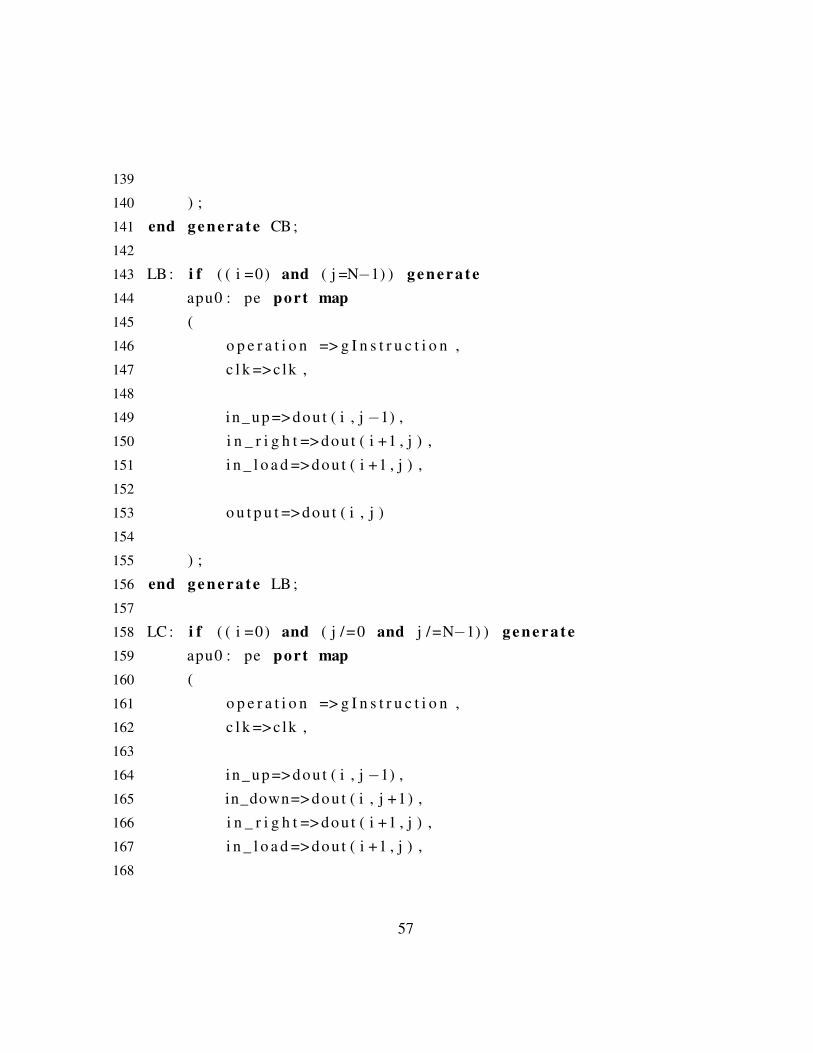
139
140 ) ;141 end g e n e r a t e CB;142
143 LB : i f ( ( i =0) and ( j =N�1) ) g e n e r a t e144 apu0 : pe port map145 (146 o p e r a t i o n => g I n s t r u c t i o n ,147 c l k => c lk ,148
149 in_up => dou t ( i , j �1) ,150 i n _ r i g h t => dou t ( i +1 , j ) ,151 i n _ l o a d => dou t ( i +1 , j ) ,152
153 o u t p u t => dou t ( i , j )154
155 ) ;156 end g e n e r a t e LB ;157
158 LC : i f ( ( i =0) and ( j /=0 and j /=N�1) ) g e n e r a t e159 apu0 : pe port map160 (161 o p e r a t i o n => g I n s t r u c t i o n ,162 c l k => c lk ,163
164 in_up => dou t ( i , j �1) ,165 in_down=> dou t ( i , j +1) ,166 i n _ r i g h t => dou t ( i +1 , j ) ,167 i n _ l o a d => dou t ( i +1 , j ) ,168
57

169 o u t p u t => dou t ( i , j )170
171 ) ;172 end g e n e r a t e LC ;173
174 CC: i f ( ( i /=0 and i /=N�1) and ( j /=0 and j /=N�1) )g e n e r a t e
175 apu0 : pe port map176 (177 o p e r a t i o n => g I n s t r u c t i o n ,178 c l k => c lk ,179
180 in_up => dou t ( i , j �1) ,181 in_down=> dou t ( i , j +1) ,182 i n _ r i g h t => dou t ( i +1 , j ) ,183 i n _ l o a d => dou t ( i +1 , j ) ,184 i n _ l e f t => dou t ( i �1, j ) ,185 o u t p u t => dou t ( i , j )186
187 ) ;188 end g e n e r a t e CC;189 end g e n e r a t e G2 ;190 end g e n e r a t e G1 ;191
192 end s t r u c t u r e ;
58