development of a multi-channel integrated circuit for use in nuclear physics experiments where...
TRANSCRIPT

Development of a Multi-Channel Integrated Development of a Multi-Channel Integrated Circuit for Use in Nuclear Physics Experiments Circuit for Use in Nuclear Physics Experiments
Where Particle Identification is ImportantWhere Particle Identification is Important
Michael HallMichael Hall
Southern Illinois University EdwardsvilleSouthern Illinois University Edwardsville
IC Design Research LaboratoryIC Design Research Laboratory
April 3, 2007April 3, 2007

22
Design TeamDesign Team
Southern Illinois University Edwardsville:Southern Illinois University Edwardsville:Dr. George Engel (PI)Dr. George Engel (PI)Michael Hall (graduate student)Michael Hall (graduate student)Justin Proctor (graduate student)Justin Proctor (graduate student)Venkata Tirumasaletty (graduate student)Venkata Tirumasaletty (graduate student)
Washington University in St. Louis:Washington University in St. Louis:Dr. Lee Sobotka (Co-PI)Dr. Lee Sobotka (Co-PI)Jon Elson (electronics specialist)Jon Elson (electronics specialist)Dr. Robert Charity Dr. Robert Charity
Western Michigan:Western Michigan:Dr. Mike Famiano (Co-PI)Dr. Mike Famiano (Co-PI)
33
Research ObjectiveResearch Objective
Design a custom microchip which can be used Design a custom microchip which can be used by nuclear physicists when they perform by nuclear physicists when they perform experiments.experiments.
In these experiments, physicists use detectors to In these experiments, physicists use detectors to sense radiation.sense radiation.
These experiments often require that the These experiments often require that the physicists identify the type of radiation (physicists identify the type of radiation (αα particle, particle, γγ-ray, etc)-ray, etc) that struck the detector. that struck the detector.
44
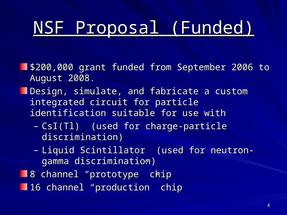
NSF Proposal (Funded)NSF Proposal (Funded)
$200,000 grant funded from September 2006 to August $200,000 grant funded from September 2006 to August 2008.2008.
Design, simulate, and fabricate a custom integrated Design, simulate, and fabricate a custom integrated circuit for particle identification suitable for use withcircuit for particle identification suitable for use with– CsI(Tl) (used for charge-particle discrimination)CsI(Tl) (used for charge-particle discrimination)– Liquid Scintillator (used for neutron-gamma Liquid Scintillator (used for neutron-gamma
discrimination)discrimination)
8 channel “prototype” chip8 channel “prototype” chip
16 channel “production” chip16 channel “production” chip

55
Intended ApplicationsIntended Applications
The chip will be used in an experiment at The chip will be used in an experiment at the National Superconducting Cyclotron the National Superconducting Cyclotron Laboratory (NSCL) in Fall 2007 by Laboratory (NSCL) in Fall 2007 by Washington University collaborators.Washington University collaborators.
Mass production of PSD technology is Mass production of PSD technology is actively being sought by our government’s actively being sought by our government’s Department of Homeland Security.Department of Homeland Security.
66
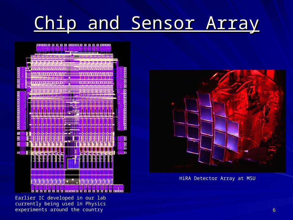
Chip and Sensor ArrayChip and Sensor Array
Earlier IC developed in our lab currently being used in Physics experiments around the country
HiRA Detector Array at MSU

77
Simulated Input Pulse for CsI(Tl) DetectorSimulated Input Pulse for CsI(Tl) Detector
IntegratorsIntegrators– A 0 to 400 nsA 0 to 400 ns
– B 1500 to 1500 nsB 1500 to 1500 ns
– C 0 to 9000 nsC 0 to 9000 ns
Integration periods at the beginning of the signal are assumed to start before the Integration periods at the beginning of the signal are assumed to start before the pulse (at -5 ns).pulse (at -5 ns).
0 1000 2000 3000 4000 5000 6000 7000 8000 9000 10000
10-2
10-1
100
MAX INPUT VOLTAGE (2V)
Plot of Alpha and Proton input pulses using a CsI(Tl) Detector for 100 MeV incident radiation
Time (ns)
Inpu
t Pul
ses
(V)
Alpha
Proton
Integrator AIntegrator B
Integrator C
88
Need for an Integrated CircuitNeed for an Integrated Circuit
Particle identification (Particle identification (αα particle, particle, γγ-ray, -ray, etc.etc.) ) capabilitycapabilityAbility to support multiple (Ability to support multiple ( i.e.i.e. initially eight but initially eight but eventually sixteen) radiation detectorseventually sixteen) radiation detectorsThree separate integration regions with Three separate integration regions with independent control of charging rate in each independent control of charging rate in each region which can be used for high-quality pulse region which can be used for high-quality pulse shape discrimination (PSD).shape discrimination (PSD).Built-in high-quality timing circuitryBuilt-in high-quality timing circuitryMultiple (3) triggering modes Multiple (3) triggering modes Data sparsificationData sparsification

99
Overview of PSD SystemOverview of PSD System
CFD
DELAY
WAWB
WC
DADB
DC
A B C T
External logic
PSD Integrator Chip
Detector
Multiplexed with other chips and sent to 4 channels of one VME Pipeline ADC
Gate control
VME
Cable
A BC
SampleIntegrationgates
Detector (PMT or photodiode)Detector (PMT or photodiode)
External discriminators External discriminators (CFDs)(CFDs)
External delay lines so we can External delay lines so we can start integrations before arrival start integrations before arrival of pulseof pulse
External control voltages External control voltages determine determine DDelay and elay and WWidth of idth of integration periodsintegration periods
Outputs A, B, C integrator Outputs A, B, C integrator voltages and relative time, Tvoltages and relative time, T

1010
ChannelChannel
3 on-chip sub-3 on-chip sub-channels for channels for integrators A, B, Cintegrators A, B, C
Delay and width of Delay and width of integrators set by integrators set by externally supplied externally supplied control voltagescontrol voltages
Timing relative to a Timing relative to a common stop signalcommon stop signal

1111
Sub-ChannelSub-Channel
Start
Control
Out
Delay Generator
Start
Control
Out
Delay Generator
Event
Dx Wx
INT-x
DUMP
ResistorArray 10 pF
DUMP
INT-x
OPAMPDAC
Control
AGND
OutDAC Setting
Input from Detector
Integrator Output
Where X = A, B, C
3
StartInt
StopInt
SUB CHANNEL
Event
DUMP
INT-x
t0
t2
t3 t5
StartInt
StopInt
t1
t4

1212
Pulse Shape Discrimination Plot for CsI(Tl) DetectorPulse Shape Discrimination Plot for CsI(Tl) Detector
Detector: Detector: CsI(Tl)CsI(Tl)Integrators:Integrators:A, BA, BEnergy Max:Energy Max:100 MeV (for 100 MeV (for 2V at input of 2V at input of integrator)integrator)Energy Range:Energy Range:1 – 100 MeV1 – 100 MeVIncludes all Includes all noise sourcesnoise sources0 50 100 150 200 250 300 350 400 450
0
100
200
300
400
500
600PSD (Pulse Shape Discrimination) Plot
Integrator A (mV)
Inte
grat
or B
(m
V)
Alpha
Proton

1313
Angular PSD Plots (CsI)Angular PSD Plots (CsI)
Detector: CsI(Tl)Detector: CsI(Tl)
Integrators: Integrators: A, BA, B
Energy Max:Energy Max:100 MeV100 MeV
Energy Range:Energy Range:1 – 100 MeV1 – 100 MeV
5000 realizations5000 realizations
Includes all noise sourcesIncludes all noise sources
40 45 50 55 60 650
200
400
600
800
1000
1200
Energy = 1 MeV, Perr = 2.16%
Theta
Cou
nt
50 51 52 53 54 55 56 57 58 59 600
500
1000
1500
2000
2500
Energy = 10 MeV, Perr = 0%
Theta
Cou
nt
Alpha Proton
51 52 53 54 55 56 57 58 590
500
1000
1500
2000
2500
3000
3500
4000
Energy = 100 MeV, Perr = 0%
Theta
Cou
nt

1414
Current WorkCurrent Work
Circuit design and simulationsCircuit design and simulations
Behavioral level simulations (VerilogA) to Behavioral level simulations (VerilogA) to verify functionality of one complete verify functionality of one complete channel including read-out electronicschannel including read-out electronics

1515
Future WorkFuture Work
LayoutLayout
FabricationFabrication– Chip should leave for fabrication in August 2007.Chip should leave for fabrication in August 2007.– Will take approximately 2 months to make.Will take approximately 2 months to make.
Testing of the ICTesting of the IC
Chip will be used in experiment at NSCL in Fall Chip will be used in experiment at NSCL in Fall 20072007