developing and analyzing lead-free soldering processes for
TRANSCRIPT
The Massachusetts Toxics Use Reduction Institute University of Massachusetts Lowell
DEVELOPING AND ANALYZING LEAD-FREE SOLDERING PROCESSES FOR
PRINTED WIRING BOARDS
TOXICS USE REDUCTION INSTITUTE UNIVERSITY RESEARCH IN SUSTAINABLE
TECHNOLOGIES PROGRAM
Technical Report No. 52 2000
University of Massachusetts Lowell

All rights to this report belong to the Toxics Use Reduction Institute. The material may be duplicated with permission bycontacting the Institute. The Toxics Use Reduction Institute is a multi-disciplinary research, education, and policy center established by the Massachusetts Toxics Use Reduction Act of 1989. The Institute sponsors and conducts research, organizes education andtraining programs, and provides technical support to promote the reduction in the use of toxic chemicals or the generation oftoxic chemical byproducts in industry and commerce. Further information can be obtained by writing the Toxics UseReduction Institute, University of Massachusetts Lowell, One University Avenue, Lowell, Massachusetts 01854. ©Toxics Use Reduction Institute, University of Massachusetts Lowell
Developing and Analyzing Lead-Free Soldering Processes for Printed Wiring Boards
Dr. Sammy Shina, P.E. and Hemant Belbase Department of Mechanical Engineering University of Massachusetts Lowell
The Toxics Use Reduction Institute University Research in Sustainable Technologies Program
The Toxics Use Reduction Institute
University of Massachusetts Lowell
2000

Table of Contents
UNIVERSITY RESEARCH IN SUSTAINABLE TECHNOLOGIES 1
ABSTRACT 2
PRINTED WIRE BOARDS AND LEAD FREE CONSIDERATIONS 2 Considerations for Lead-Free Soldering Implementation 3
FACTOR SELECTION 4 Materials 4
Solder Alloys and Flux 4 Specific Alloy Compositions Reviewed and/or Recommended by Other Organizations [1] 4 Fluxes 5 Components 6 Die Attach 7 Ball Grid Array and Chip Scale Packaging Alternatives 7 Flip Chip 7 Connectors/Through Hole 7
PWB Finishes 7 Organic Solder Proctectants (OSPs) 8 Lead-Free Hot Air Solder Level 8 Immersion Finishes 8 Electroless NiAu (Electroless Nickel Immersion Gold) 8
ENVIRONMENTAL IMPACTS AND TOXICITY OF LEAD FREE SOLDERS 9 Toxicity 9 Leaching 9
EXPERIMENTATION 10 Setup and Experiment Design 10
Experiment Matrix 11 Strategy 11 Profiles 12 Time Above Liquidus (TAL) 13 Reflow Environment 14
Test Vehicle 14 Components 14 Stencil 15 Screen Printer 15 Oven (BTU Paragon 150) 16 Final Assembly 16 Experimental Run 16
RESULTS 16 Test Method and Defect Count 17
Defect Count 17 Visual defect results 18
ANOVA Analysis of Visual Results 19 Visual Results Conclusions 19
CURRENT STATUS OF THE PROJECT 20

ACKNOWLEDGMENTS 20
SPONSORSHIP 21
REFERENCES 21
UNIVERSITY RESEARCH IN SUSTAINABLE TECHNOLOGIES
The University Research in Sustainable Technologies program is a joint project of the Toxics Use Reduction Institute (TURI) and the Center for Environmentally Appropriate Materials (CEAM) at the University of Massachusetts Lowell, with support from the Commonwealth’s STrategic Envirotechnology Partnership (STEP). The program taps the research capabilities of the University of Massachusetts to advance the investigation, development and evaluation of sustainable technologies that are environmentally, occupationally and economically sound. The program provides research funding to UMass faculty from all campuses, annually, on a competitive basis and encourages faculty/industry partnerships and cross-campus collaboration. Industry partners provide guidance, propose applications for new technologies, and, in some cases, evaluate and/or adopt processes and technologies resulting from research. Following is a list of the Fiscal Year 2000 projects. • Developing and Analyzing Lead-Free Soldering Processes for Printed Wiring Boards - Prof.
Sammy G. Shina, UMass Lowell, Department of Mechanical Engineering • Diffusion Dialysis and Acid Recovery in Metal Woking and Finishing - Prof. Francis J. Bonner
and Prof. Alfred A. Donatelli, UMass Lowell, Department of Chemical Engineering • Solar Fuel Cell System - Prof. John Duffy, UMass Lowell, Department of Mechanical Engineering,
Solar Engineering Program • Optical Information Processing with Environmentally Friendly Organic Materials - Prof.
D.V.G.L.N. Rao, UMass Boston, Department of Physics • Environmentally Benign Control of Polymer Solubility: Photoresist Materials Using DNA
Mimics - Prof. John C. Warner, UMass Boston, Department of Chemistry • Integration of Pollution Prevention and Occupational Health and Safety - Prof. Rafael Moure-
Eraso, UMass Lowell, Department of Work Environment • Synthesis of Conjugated Polymers and Molecules Using Sugar Reagents and Solventless
Reactions - Prof. Daniel J. Sandman, UMass Lowell, Department of Chemistry Notice This report has been reviewed by the Institute and approved for publication. Approval does not signify that the contents necessarily reflect the views and policies of the Toxics Use Reduction Institute, nor does the mention of trade names or commercial products constitute endorsement or recommendation for use.

2
ABSTRACT
As the European and global marketplaces consider mandating lead-free electronic equipment, many questions arise about the technical feasibility of replacing lead in Printed Wiring Board (PWB) soldering applications.
Researchers on this project formed an industry-led “UMASS Lead-Free Consortium” (the Consortium) of local and national companies to evaluate various emerging alternatives to lead-based solders and finishes. The consortium members donated expertise, time, materials and equipment to this project. The various alternatives to lead-bearing materials, surface finishes and manufacturing processes were evaluated as factors in a set of designed experiments, and compared the results to a baseline of standard leaded processes and materials, using the quality characteristics of visual, mechanical and thermal testing criteria. The Manufacturing Research Laboratory facilities at UMASS Lowell were utilized to test and analyze the performance of alternatives based on the principles of Design of Experiments. Results were analyzed using statistical techniques resulting in determining whether a particular factor was significant to the quality characteristic being measured. A theoretical percent contribution to the total quality characteristic was calculated for significant factors.
The results of this research showed that PWB assembly with zero defects and stronger solder joints could be achieved using lead-free alternatives as opposed to the more traditional tin-lead baseline. Among the lead-free alternatives selected in this research and, based on their statistical analysis, tin-silver-copper and Electroless Nickel Immersion Gold (ENIG) were found to be the most suitable selections for solder paste alloy and PWB surface finish, respectively. Similarly, nitrogen and linear thermal profile were recommended as significant process parameters. PRINTED WIRE BOARDS AND LEAD FREE CONSIDERATIONS
The printed wiring board (PWB) is the building block of the electronics industry. It is the underlying link between semiconductors, computer chips, and other electronic components. However, traditional methods for manufacturing PWBs use toxic chemicals that pose potential health and environmental risks, generate large volumes of hazardous waste, and use substantial amounts of water and energy.
The tremendous increase in the usage of consumer electronics products and decreasing life cycles of these products have raised the issues of recycling and electronics waste in landfills. As a result, there are major concerns of lead being leached into water supplies from discarded printed wiring board (PWB) assembly (1). These concerns are the driving forces for various legislative draft proposals around the world to ban the use of leaded solder (1).
Lead, although a toxic material, has been widely used in human civilization since Roman times. One of the common uses is in tin-lead eutectic solders, which have been extensively used in the manufacturing of electronic products for more than fifty years. These solders (usually 60/40 tin-lead) have predominated because they are inexpensive relative to other alloys and perform reliably under a variety of operating conditions. In addition, they possess unique characteristics such as low melting point, high strength, ductility, fatigue resistance, high thermal cycling, electrical conductivity and joint integrity that are well suited for electronic product applications. Leaded solders perform the following three basic functions in electronics interconnection:
They provide the final surface finish for printed wiring boards;
They are applied to component leads to achieve a compatible solderable surface; and
They are used to attach electronic components on printed wiring boards.

3
As the European and global marketplaces consider mandating lead-free electronic equipment, many questions arise about the technical feasibility of replacing lead in PWBs soldering applications.
Considerations for Lead-Free Soldering Implementation
Some of the considerations to implementation of lead-free soldering alternatives have been identified as: • Process requirements; • Requirement for multiple finishes; • Performance and reliability associated with alternatives; • The potential toxicity and environmental impacts of alternatives; • Environmental requirements associated with lead-free soldering applications may not be uniform or
stable, therefore industry must monitor its activities accordingly; • Fire safety issues may be a concern with certain higher-temperature solders; • Worker safety/exposure issues must be considered; • Equipment limitations may impact cost effectiveness of the process; • Additional lead free lines may be required during transition; • Lack of industry partnerships may make the identification of suitable alternatives difficult; • Higher reflow temperatures increase warpage; • Higher reflow temperatures cause stress on printed through holes; and • Higher temperatures required for lead-free may affect the selection of inks, adhesives, and markings. The United States Environmental Protection Agency's Design for the Environment (DfE) Project has identified the following additional issues that must be considered when evaluating lead-free soldering alternatives: • Higher temperature stability; • Solder processes; • Long term reliability; • What is lead free (need more definition – possible <0.02%); • Recycling requirements; • Finishes must be SnPb compatible; • Rework and repair impact; • Inspection and quality criteria; • Impact on standards and specifications; • Good global source of supply; • Marking for lead-free PWBs; and • Impact on solder mask.

4
FACTOR SELECTION
Materials
Solder Alloys and Flux
There are numerous lead-free alloys available today, some of which have been used regularly. High-temperature alloys have been used successfully in under-hood applications, and some companies worked these alloys into their processes for consumer and military/aerospace applications. It should be noted that once a lead-free alloy has been chosen, the qualification of the process could take as long as two years. The following table lists some known alloys [1]
Table 1. Commonly Used Alloys in Soldering Operations
ALLOYS USED MELTING RANGE (°C)
INDUSTRY SERVED COMPANY
SnAg 221 – 226 Automotive Visteon (Ford) Military/Aerospace Panasonic SnAgBi 206 – 213
Consumer Hitachi SnAgBiCu Military/Aerospace Panasonic
SnAgBiCuGe Consumer Sony SnAgBiX 206 – 213 Consumer Panasonic
Automotive Panasonic Nokia Nortel
Panasonic
SnAgCu 217 Telecommunications
Toshiba SnBi 138 Consumer Panasonic
Consumer Panasonic SnCu 227 Telecommunications Nortel
NEC Panasonic
SnZn 198.5 Consumer
Toshiba
Specific Alloy Compositions Reviewed and/or Recommended by Other Organizations [1]
SnAgCu
The tin-silver-copper (SnAgCu) alloy composition (with or without the addition of a fourth element) appears to be the most popular replacement for tin-lead (SnPb) solders. This alloy has also been chosen to be the benchmark, with SnPb being the baseline, for testing any other alloys to be included in the research.
Concerns with this alloy family include higher processing temperatures and their compatibility with lead-bearing finishes. It should also be noted that metals costs for this alloy were about 2.2 to 2.7 times that of the SnPb eutectic at year 2000 market values.

5
SnCu
The tin-copper (SnCu) alloy composition is a low cost alternative for wave soldering, it's main area of use, and is compatible with most lead-bearing finishes. Process considerations must be addressed with this alloy, which has a higher melting temperature than most SnAgCu alloys. This alloys was also 1.5 times more expensive than SnPb eutectic at year 2000 market values.
SnAgBi
The tin-silver-bismuth (SnAgBi) alloy has been chosen as a candidate alloy, especially for use in surface mount technology (SMT) applications. The major concerns of bismuth are fillet lifting (which occurs in SnPb through-hole applications) and its toxicity.
According to the National Center for Manufacturing Sciences (NCMS) study, SnAgBi has better thermal cycle reliability for certain surface mount components than SnAgCu, using 1206 resistors and capacitors with lead-free finishes and PWBs with lead-free finishes. The study also showed this alloy as having better wetting characteristics than SnAg and SnAgCu. Metals costs for this alloy were 2.2 to 2.7 times more that of SnPb eutectic at year 2000 market values.
SnZn
Although the tin-zinc (SnZn) alloy has lower melting temperatures (<200°C), there are concerns with the oxidation of zinc and the long-term corrosion of the finished solder joint. This alloy also requires special fluxes, and its wetting characteristics don’t compare well to those of SnAgCu. Industrial applications should likely wait for more long-term data for this alloy to determine if it is a technically and economically feasible alternative.
SnAg
The tin-silver (SnAg) alloy has a slightly higher melting point (221°C) than SnAgCu, and is comparably priced to this alloy. Because it has been used for years in step soldering and special applications (i.e., die attach), there is an extensive database on its available applicability.
Fluxes
Selection of a new soldering alloy will require deviations in flux chemistries used. Industries can’t plan on using an existing flux in the new soldering process. Industries can expect to have to tweak their current chemistries for high-temperature alloys, and possibly use entirely different chemistries (e.g., for zinc-based alloys).
Variations in flux chemistries will also affect the cleaning process, solder mask, coating, and materials. If voiding occurs after making the transition, the user may need to work with solvent or resin systems to alleviate the problem.
Industry trade organizations recommend the use of various fluxes in lead-free soldering operations, as indicated in Table 2.

6
Table 2. Flux Alloys Recommended by Industry Trade Organizations
Organization Flux Alloy Compositions Recommended
National Electronics Manufacturing Initiative
(NEMI)
Sn-0.7Cu Sn-3.5Ag Sn-Ag-Cu
National Center for Manufacturing Sciences
(NCMS)
Sn-3.5Ag Sn-58Bi Sn-3.0Ag-2.0Bi CASTIN Sn-3.4Ag-4.8Bi Sn-20In-2.8Ag (Indalloy) Sn-3.5Ag-0.5Cu-1.0Zn
International Tin Research Institute (ITRI)
Sn-Ag-Cu Sn-2.5Ag-0.8Cu-0.5Sb Sn-0.7Cu Sn-3.5Ag Sn-Bi-Ag Sn-Bi-Zn
There are few studies done on the compatibility of existing flux chemistries with lead-free alloys. A recent study [2] concluded with the requirement of no clean, high residue and high activity flux for good quality solder joints, using SnAg and SnAgCu alloy with three different type of flux.
Components
Several types of lead-free component finishes are available to the industry and have been successfully used in assembly operations. However, there are concerns over cost, reliability, and workability with lead-free alloys due to factors such as higher melting temperatures.
For those companies who choose to use components with lead-bearing finishes, there is also the concern of fillet lifting resulting from the use of some lead-free alloys. Although the fillet lifting does not occur in all circumstances of through hole or surface mounting applications, it is an important consideration for companies in deciding whether to use alternative component finishes.
Available Components
The most common alloy used in component finishes is palladium, which is usually used with nickel, silver or as a stand-alone finish. Some other concerns expressed by industry include requalification that may be needed for temperature-sensitive components
Molded Components
With molded components there are concerns about "pop-corning" and delamination with the use of lead free solders. Concerns also exist about the time needed to identify new materials (e.g., molding compounds) and temperature-sensitive components that may need time for requalification and redesign. Molding compounds developed to meet the higher temperature lead-free requirements should also meet the
7
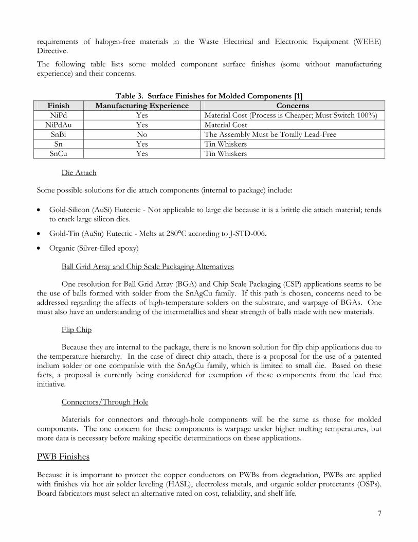
requirements of halogen-free materials in the Waste Electrical and Electronic Equipment (WEEE) Directive.
The following table lists some molded component surface finishes (some without manufacturing experience) and their concerns.
Table 3. Surface Finishes for Molded Components [1]
Finish Manufacturing Experience Concerns NiPd Yes Material Cost (Process is Cheaper; Must Switch 100%)
NiPdAu Yes Material Cost SnBi No The Assembly Must be Totally Lead-Free Sn Yes Tin Whiskers
SnCu Yes Tin Whiskers
Die Attach
Some possible solutions for die attach components (internal to package) include: • Gold-Silicon (AuSi) Eutectic - Not applicable to large die because it is a brittle die attach material; tends
to crack large silicon dies.
• Gold-Tin (AuSn) Eutectic - Melts at 280°C according to J-STD-006.
• Organic (Silver-filled epoxy)
Ball Grid Array and Chip Scale Packaging Alternatives
One resolution for Ball Grid Array (BGA) and Chip Scale Packaging (CSP) applications seems to be the use of balls formed with solder from the SnAgCu family. If this path is chosen, concerns need to be addressed regarding the affects of high-temperature solders on the substrate, and warpage of BGAs. One must also have an understanding of the intermetallics and shear strength of balls made with new materials.
Flip Chip
Because they are internal to the package, there is no known solution for flip chip applications due to the temperature hierarchy. In the case of direct chip attach, there is a proposal for the use of a patented indium solder or one compatible with the SnAgCu family, which is limited to small die. Based on these facts, a proposal is currently being considered for exemption of these components from the lead free initiative.
Connectors/Through Hole
Materials for connectors and through-hole components will be the same as those for molded components. The one concern for these components is warpage under higher melting temperatures, but more data is necessary before making specific determinations on these applications. PWB Finishes
Because it is important to protect the copper conductors on PWBs from degradation, PWBs are applied with finishes via hot air solder leveling (HASL), electroless metals, and organic solder protectants (OSPs). Board fabricators must select an alternative rated on cost, reliability, and shelf life.
8
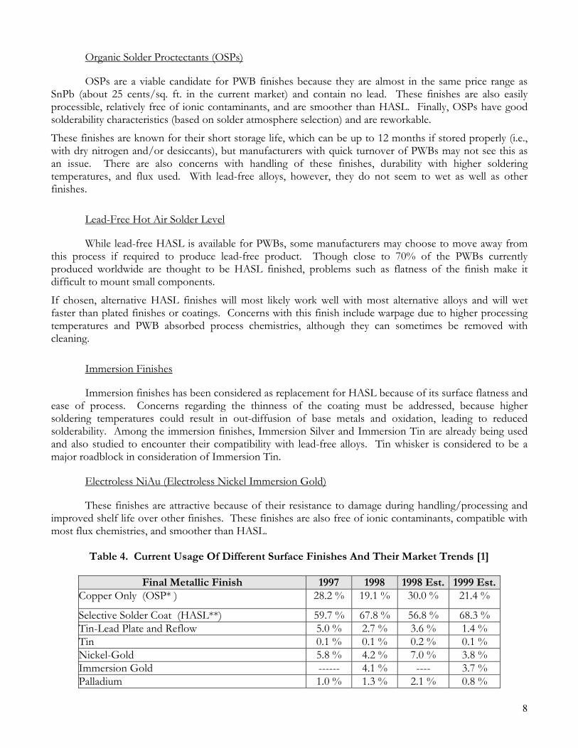
Organic Solder Proctectants (OSPs)
OSPs are a viable candidate for PWB finishes because they are almost in the same price range as SnPb (about 25 cents/sq. ft. in the current market) and contain no lead. These finishes are also easily processible, relatively free of ionic contaminants, and are smoother than HASL. Finally, OSPs have good solderability characteristics (based on solder atmosphere selection) and are reworkable.
These finishes are known for their short storage life, which can be up to 12 months if stored properly (i.e., with dry nitrogen and/or desiccants), but manufacturers with quick turnover of PWBs may not see this as an issue. There are also concerns with handling of these finishes, durability with higher soldering temperatures, and flux used. With lead-free alloys, however, they do not seem to wet as well as other finishes.
Lead-Free Hot Air Solder Level
While lead-free HASL is available for PWBs, some manufacturers may choose to move away from this process if required to produce lead-free product. Though close to 70% of the PWBs currently produced worldwide are thought to be HASL finished, problems such as flatness of the finish make it difficult to mount small components.
If chosen, alternative HASL finishes will most likely work well with most alternative alloys and will wet faster than plated finishes or coatings. Concerns with this finish include warpage due to higher processing temperatures and PWB absorbed process chemistries, although they can sometimes be removed with cleaning.
Immersion Finishes
Immersion finishes has been considered as replacement for HASL because of its surface flatness and ease of process. Concerns regarding the thinness of the coating must be addressed, because higher soldering temperatures could result in out-diffusion of base metals and oxidation, leading to reduced solderability. Among the immersion finishes, Immersion Silver and Immersion Tin are already being used and also studied to encounter their compatibility with lead-free alloys. Tin whisker is considered to be a major roadblock in consideration of Immersion Tin.
Electroless NiAu (Electroless Nickel Immersion Gold)
These finishes are attractive because of their resistance to damage during handling/processing and improved shelf life over other finishes. These finishes are also free of ionic contaminants, compatible with most flux chemistries, and smoother than HASL.
Table 4. Current Usage Of Different Surface Finishes And Their Market Trends [1]
Final Metallic Finish 1997 1998 1998 Est. 1999 Est.Copper Only (OSP* ) 28.2 % 19.1 % 30.0 % 21.4 %
Selective Solder Coat (HASL**) 59.7 % 67.8 % 56.8 % 68.3 % Tin-Lead Plate and Reflow 5.0 % 2.7 % 3.6 % 1.4 % Tin 0.1 % 0.1 % 0.2 % 0.1 % Nickel-Gold 5.8 % 4.2 % 7.0 % 3.8 % Immersion Gold ------ 4.1 % ---- 3.7 % Palladium 1.0 % 1.3 % 2.1 % 0.8 %

9
Final Metallic Finish 1997 1998 1998 Est. 1999 Est.Tin-Nickel 0.2 % 0.4 % 0.2 % 0.2 % Other 0.1% 0.2 % 0.1 % 0.1 % Total 100.0 % 100.0 % 100.0 % 100.0 %
ENVIRONMENTAL IMPACTS AND TOXICITY OF LEAD FREE
SOLDERS
The goal of this project is not to suggest a prohibition on lead-free solders, but to assist industry in selecting the best alloy from many alternatives. Factors that should be considered when selecting alloys include the associated environmental impacts as well as the toxicity of the alloys. This section presents a discussion of these factors. Toxicity
The Surface Mount Council, in its report referenced earlier, provides information on the relative toxicity of the various lead-free soldering elements. The following table presents this data.
Table 5. Relative Toxicity of Metals Common to Soldering Alloys
Metal Element OSHA PEL or ACGIH TLV (mg/m3)
Bismuth None Zinc Oxide (Fume) 5
Tin (Inorganic) 2 Tin (Organic) 0.1
Antimony 0.5 Copper (Dust) 1 Copper (Fume) 0.1
Indium 0.1 Silver (Metal Dust and Fume) 0.1a
Silver (and Soluble Compounds) 0.01b Lead (Inorganic) 0.05c
a: OSHA PEL, b: ACGIH TLV c: ACGIH TLV is 0.15 mg/m3 Based on this data and other data [3] cited in its report, the Surface Mount Council assigns this toxicity ranking to the common lead free solder alloying elements:
Bi < Zn < In < Sn < Cu < Sb < Ag < Pb Leaching
There are not many reference that compare lead free solders with tin/lead solder in terms of their leaching effect. More work needs to be done in this area. The main concern raised in the current WEEE draft proposal and in JAPAN has been leaching due to electronic wastes into landfill sites. Results from a study (Environmental Impacts And Toxicity Of Lead Free Solders by Edwin B. Smith [4]) that compares eight lead free alloys and tin/lead solder for their leaching effect. The experimental leaching

10
results compared with available toxicity data, for the alloys studied is presented in Table 6 in order of increasing environmental and occupational impacts.
Table 6. Toxicity of Lead-Free Solder Alloys
43 Tin • 57 Bismuth Least Impact 80 Tin • 20 Indium
99.3 Tin • 0.7 Copper 90 Tin • 5 Bismuth
5 Silver 98 Tin • 2 Silver
96.5 Tin • 3.2 Silver 0.5 Copper
95 Tin • 5 Antimony Greater Impact
EXPERIMENTATION
With all the options presented, input from project team members and through many brainstorming sessions, it was finally concluded to direct this study into the development of a lead-free electronic assembly process. Since lead-free soldering currently has too many options but no solutions the experimental setup had to be a roadmap towards optimization of current process into a lead-free process.
In order to fulfill this objective and to see the contribution and effect of each in the process the setup had to be a designed experiment that can be analyzed statistically.
The following are considered to be the investigating factors:
• Lead-free solder paste alloys;
• PWB surface finish;
• Thermal Profiles of the alloys;
• Lead-free component lead finish;
• Reflow environment; and
• Tin-Lead baseline for direct comparison. Setup and Experiment Design
Five factors were considered with mixed:
Paste (3 levels);
• PWB Surface Finish (originally 3, then 2 levels);
• Time Above Liquidus (TAL) (3 levels);
• Soak (2 levels); and
• Nitrogen (2 levels).
11
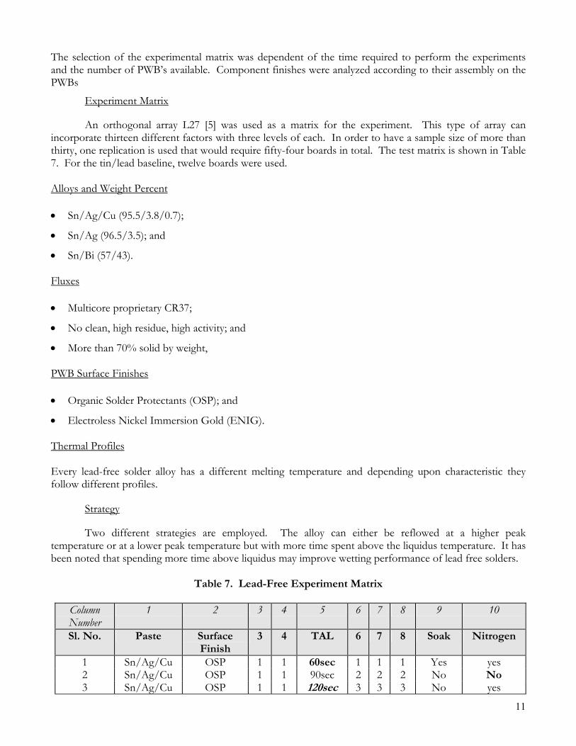
The selection of the experimental matrix was dependent of the time required to perform the experiments and the number of PWB’s available. Component finishes were analyzed according to their assembly on the PWBs
Experiment Matrix
An orthogonal array L27 [5] was used as a matrix for the experiment. This type of array can incorporate thirteen different factors with three levels of each. In order to have a sample size of more than thirty, one replication is used that would require fifty-four boards in total. The test matrix is shown in Table 7. For the tin/lead baseline, twelve boards were used. Alloys and Weight Percent • Sn/Ag/Cu (95.5/3.8/0.7);
• Sn/Ag (96.5/3.5); and
• Sn/Bi (57/43). Fluxes • Multicore proprietary CR37;
• No clean, high residue, high activity; and
• More than 70% solid by weight, PWB Surface Finishes • Organic Solder Protectants (OSP); and
• Electroless Nickel Immersion Gold (ENIG). Thermal Profiles Every lead-free solder alloy has a different melting temperature and depending upon characteristic they follow different profiles.
Strategy
Two different strategies are employed. The alloy can either be reflowed at a higher peak temperature or at a lower peak temperature but with more time spent above the liquidus temperature. It has been noted that spending more time above liquidus may improve wetting performance of lead free solders.
Table 7. Lead-Free Experiment Matrix
Column Number
1 2 3 4 5 6 7 8 9 10
Sl. No. Paste Surface Finish
3 4 TAL 6 7 8 Soak Nitrogen
1 Sn/Ag/Cu OSP 1 1 60sec 1 1 1 Yes yes 2 Sn/Ag/Cu OSP 1 1 90sec 2 2 2 No No 3 Sn/Ag/Cu OSP 1 1 120sec 3 3 3 No yes

12
Column Number
1 2 3 4 5 6 7 8 9 10
Sl. No. Paste Surface Finish
3 4 TAL 6 7 8 Soak Nitrogen
4 Sn/Ag/Cu ENIG 2 2 60sec 1 1 2 No No 5 Sn/Ag/Cu ENIG 2 2 90sec 2 2 3 No yes 6 Sn/Ag/Cu ENIG 2 2 120sec 3 3 1 Yes yes 7 Sn/Ag/Cu OSP 3 3 60sec 1 1 3 No yes 8 Sn/Ag/Cu OSP 3 3 90sec 2 2 1 Yes yes 9 Sn/Ag/Cu OSP 3 3 120 3 3 2 No No 10 Sn/Bi OSP 2 3 60sec 2 3 1 No yes 11 Sn/Bi OSP 2 3 90sec 3 1 2 No yes 12 Sn/Bi OSP 2 3 120sec 1 2 3 Yes No 13 Sn/Bi ENIG 3 1 60sec 2 3 2 No yes 14 Sn/Bi ENIG 3 1 90sec 3 1 3 Yes No 15 Sn/Bi ENIG 3 1 120sec 1 2 1 No yes 16 Sn/Bi OSP 1 2 60sec 2 3 3 Yes No 17 Sn/Bi OSP 1 2 90sec 3 1 1 No yes 18 Sn/Bi OSP 1 2 120sec 1 2 2 No yes 19 Sn/Ag OSP 3 2 60sec 3 2 1 No No 20 Sn/Ag OSP 3 2 90sec 1 3 2 Yes yes 21 Sn/Ag OSP 3 2 120sec 2 1 3 No yes 22 Sn/Ag ENIG 1 3 60sec 3 2 2 Yes yes 23 Sn/Ag ENIG 1 3 90sec 1 3 3 No yes 24 Sn/Ag ENIG 1 3 120sec 2 1 1 No No 25 Sn/Ag OSP 2 1 60sec 3 2 3 No yes 26 Sn/Ag OSP 2 1 90sec 1 3 1 No No 27 Sn/Ag OSP 2 1 120sec 2 1 2 Yes yes
Table Notes: • Columns 11, 12 and 13 are not shown, but follow the patterns of L27 Orthogonal arrays • Columns 3 and 4 are interactions between Solder Paste and Surface Finish • Columns 6 and 7 are interactions between solder paste and time above liquidus • Columns 8 and 11 are interactions between surface finishes and time above liquidus Table Acknowledgements:
PWBs manufactured and supplied by Sanmina (formerly Hadco Corporation.) Thermal profiles developed at BTU International. Solder Paste and Flux supplied by Multicore Solders. Components supplied by Texas Instruments and BTU International. Reflow environment supplied by Solectron Corporation. Final assembly, completed at Solectron Corporation.
Profiles
Two different types of profiles for each alloy were considered: 1. Conventional Soak Profile; and
2. Linear Profile
13
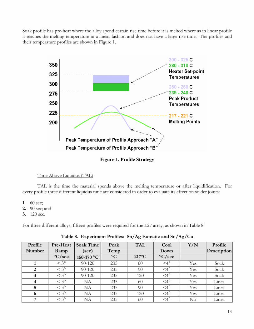
Soak profile has pre-heat where the alloy spend certain rise time before it is melted where as in linear profile it reaches the melting temperature in a linear fashion and does not have a large rise time. The profiles and their temperature profiles are shown in Figure 1.
Figure 1. Profile Strategy
Time Above Liquidus (TAL)
TAL is the time the material spends above the melting temperature or after liquidification. For every profile three different liquidus time are considered in order to evaluate its effect on solder joints: 1. 60 sec; 2. 90 sec; and 3. 120 sec. For three different alloys, fifteen profiles were required for the L27 array, as shown in Table 8.
Table 8. Experiment Profiles: Sn/Ag Eutectic and Sn/Ag/Cu
Profile Pre-Heat Soak Time Peak TAL Cool Y/N Profile Number Ramp (sec) Temp Down Description
°C/sec 150-170 °C °C 217°C °C/sec 1 < 3° 90-120 235 60 <4° Yes Soak 2 < 3° 90-120 235 90 <4° Yes Soak 3 < 3° 90-120 235 120 <4° Yes Soak 4 < 3° NA 235 60 <4° Yes Linea 5 < 3° NA 235 90 <4° Yes Linea 6 < 3° NA 235 120 <4° Yes Linea 7 < 3° NA 235 60 <4° No Linea

14
Profile Pre-Heat Soak Time Peak TAL Cool Y/N Profile Number Ramp (sec) Temp Down Description
°C/sec 150-170 °C °C 217°C °C/sec 8 < 3° NA 235 90 <4° No Linea 9 < 3° NA 235 120 <4° No Linea 10 <2° 60-120 168 60 <4° No Soak 11 <2° 60-120 168 90 <4° No Soak 12 <2° 60-120 168 120 <4° No Soak 13 <2° NA 168 60 <4° Yes Linea 14 <2° NA 168 90 <4° Yes Linea 15 <2° NA 168 120 <4° Yes Linea
Note: Peak Temperatures are + 5 °C
Reflow Environment
In SMT application creating an inert atmosphere inside the oven does have an effect on the quality of solder joints. Different environment is employed in the existing lead based process. In this investigation, existing two different environment are employed; 1. Nitrogen 2. Air Test Vehicle
The test vehicle (5.5"x4.0") used is a single layer PWB made of FR-4 material. It was manufactured in one lot by Sanmina Corporation. The experiment required two different surface finishes: half of them had OSPs and the other half had Electroless Nickel Immersion Gold as surface finish over pads. The experimental Test Vehicle is shown in Figure 2.
Components
The test vehicle is partially filled with the following components:
Passives Quantity Lead Finish 1206 24 Tin 805 42 Tin 402 27 Tin
IC/Semiconducto
r
Quantity
Lead Finish
LQFP 120 2 Ni/Pd LQFP 100 2 Ni/Pd
SO16 3 Ni/Pd SO14 3 Ni/Pd
For the Tin-Lead baseline, the same components with tin-lead finish are used.

15
Figure 2. Test Vehicle
Stencil
• Size 29" x 29";
• Foil thickness: 6 mil stepped to 4 mils;
• Laser Cut;
• Stencil aperture openings determined as well as the most appropriate aspect ratio;
• R0402 parts are to be 100%;
• All 20 and 25 mil pitch parts are to have width only reduced by 10%;
• Aperture length 100%;
• TSOP32: Aperture width reduced to 10mils. Aperture length is 100%;
• TQFP120 (.008 x .065 pads): Stepped down to 4-mil thickness. Width reduced only by 10%. Aperture length 100%;
• TQFP120 (.010 x .065 pads): Stepped down to 4-mil thickness. Width reduced to 8 mils. Aperture length 100%;
• TQFP168 (.008 x .065 pads): Stepped down to 4-mil thickness. Width reduced only by 10%. Aperture length 100%; and
• TQFP168 (.006 x .065 pads): Stepped down to 4-mil thickness. Width 100%. Aperture length 100%.
Screen Printer
MPM Ultrapoint 3000 series Squeeze Blade: Provided by Solectron Massachusetts • Total Force (12.0 lb);
• Balance (50/50);
• Down Step (0.075);
• Print Speed (1.0"/second);
• Printing Condition;
• Room Temp (between 70 and 80°F); and

16
• Humidity (65%).
Oven (BTU Paragon 150)
• Since the test vehicle is small insulator in between the zone was used to save heat loss; and
• Winkic profile viewer was used to develop profiles.
Final Assembly
• Fifty four boards assembled using three different lead free solders and lead free lead finish components;
• Twelve boards assembled using Tin-lead solder and Tin lead finish components; and
• All Fifty six boards assembled without disturbing the setup in order to reduce experimental errors.
Experimental Run
• Run dependent upon solder paste alloy;
• Started off with Sn/Bi followed by Sn/Ag, Sn/Ag/Cu and then Sn/Pb; and
• Every time solder paste was changed stencil and squeeze blade were cleaned properly to avoid any contamination.
RESULTS
Results were measured in the following areas: • Visual Defect Test;
• Pull test; and
• Thermal Cycling reliability.
Table 9. Visual Defect Test – Total Defect Opportunities Component Quantity Defect Opportunities Total1 LQFP 100 2 100 2002 LQFP 120 2 120 2403 SO16 3 16 48 4 SO14 3 14 42 5 1206 24 2 48 6 0805 42 2 84 7 0402 27 2 54 Following are pads considered only for defect opportunities:
8 QFP 100 2 100 2009 SOT 23 6 3 18 10 PLCC 28 2 28 56 11 BGA 225 1 225 22512 TSOP 32 2 32 64 Total 1279

17
Test Method and Defect Count
Visual inspection of solder joints: • IPC JSTD-001 followed as guideline • Lens Magnification 0.7 X 10x
Defect Count
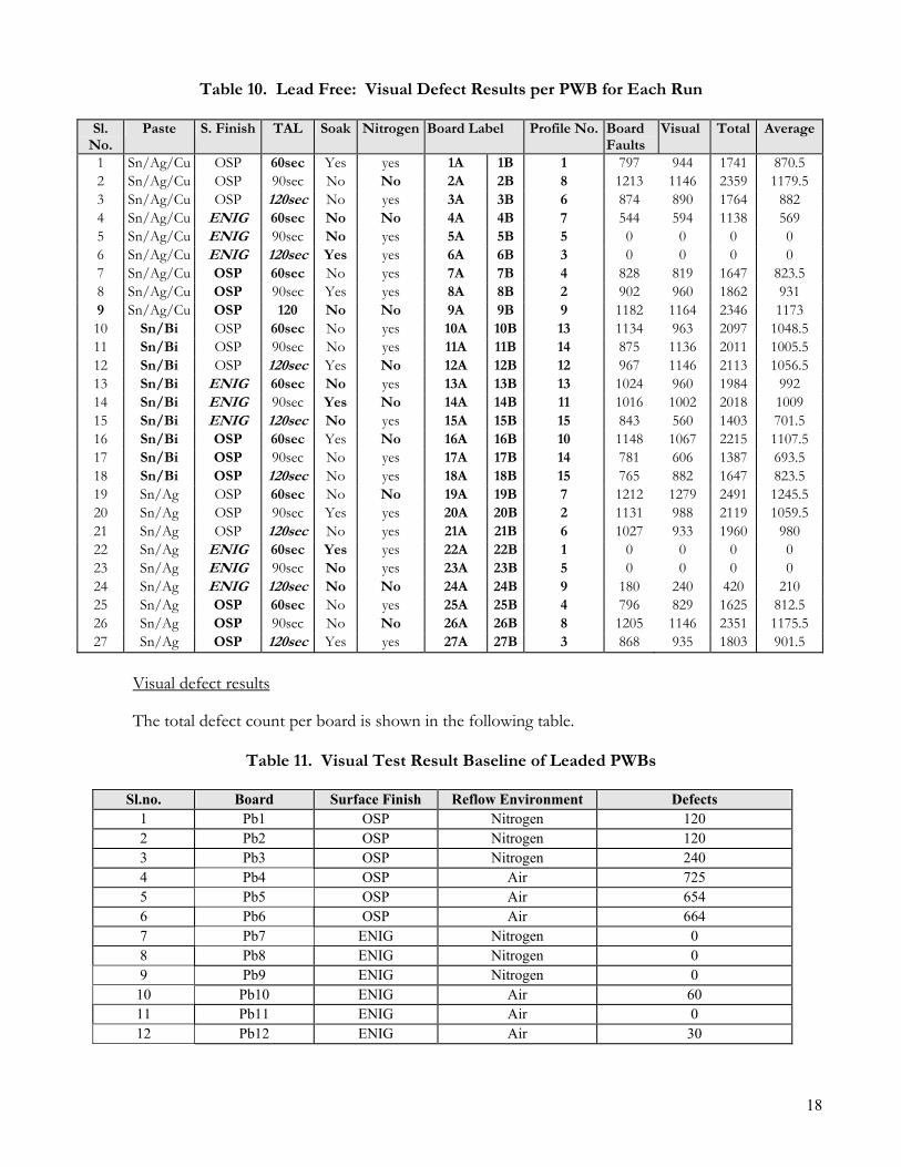
• Fillet • Poor wetting • Bridging • Solder balls Lead-free solders do not seem to wet very well as compared to tin-lead solder. Most of the defects encountered were due to poor wetting and fillets. Since the flux employed is a no-clean, high activity, high residue type most of the boards had high flux residue. At first glance it could be observed that the solders did not reflow as expected. This could be due to the metallurgical behavior of the materials of solder and surface finish. Since wetting characteristic of the solder will depend upon the metallurgy of component lead and pad surface finish this was not of a surprise. It would be interesting to analyze different lead-free solders behavior with different options. Visually OSP finished boards seemed to have more defects than the "Electroless Nickel Immersion Gold (ENIG)" finished boards. It was also observed that nitrogen did improve the wetting characteristic of the solder. Tin-lead baseline had no different behavior than the lead-free setup. Although the defect counts was less than the lead free they followed the same behavior for OSP and ENIG surface finish and nitrogen reflow environment.
18
Table 10. Lead Free: Visual Defect Results per PWB for Each Run
Sl. No.
Paste S. Finish TAL Soak Nitrogen Board Label Profile No. Board Faults
Visual Total Average
1 Sn/Ag/Cu OSP 60sec Yes yes 1A 1B 1 797 944 1741 870.5 2 Sn/Ag/Cu OSP 90sec No No 2A 2B 8 1213 1146 2359 1179.5 3 Sn/Ag/Cu OSP 120sec No yes 3A 3B 6 874 890 1764 882 4 Sn/Ag/Cu ENIG 60sec No No 4A 4B 7 544 594 1138 569 5 Sn/Ag/Cu ENIG 90sec No yes 5A 5B 5 0 0 0 0 6 Sn/Ag/Cu ENIG 120sec Yes yes 6A 6B 3 0 0 0 0 7 Sn/Ag/Cu OSP 60sec No yes 7A 7B 4 828 819 1647 823.5 8 Sn/Ag/Cu OSP 90sec Yes yes 8A 8B 2 902 960 1862 931 9 Sn/Ag/Cu OSP 120 No No 9A 9B 9 1182 1164 2346 1173 10 Sn/Bi OSP 60sec No yes 10A 10B 13 1134 963 2097 1048.5 11 Sn/Bi OSP 90sec No yes 11A 11B 14 875 1136 2011 1005.5 12 Sn/Bi OSP 120sec Yes No 12A 12B 12 967 1146 2113 1056.5 13 Sn/Bi ENIG 60sec No yes 13A 13B 13 1024 960 1984 992 14 Sn/Bi ENIG 90sec Yes No 14A 14B 11 1016 1002 2018 1009 15 Sn/Bi ENIG 120sec No yes 15A 15B 15 843 560 1403 701.5 16 Sn/Bi OSP 60sec Yes No 16A 16B 10 1148 1067 2215 1107.5 17 Sn/Bi OSP 90sec No yes 17A 17B 14 781 606 1387 693.5 18 Sn/Bi OSP 120sec No yes 18A 18B 15 765 882 1647 823.5 19 Sn/Ag OSP 60sec No No 19A 19B 7 1212 1279 2491 1245.5 20 Sn/Ag OSP 90sec Yes yes 20A 20B 2 1131 988 2119 1059.5 21 Sn/Ag OSP 120sec No yes 21A 21B 6 1027 933 1960 980 22 Sn/Ag ENIG 60sec Yes yes 22A 22B 1 0 0 0 0 23 Sn/Ag ENIG 90sec No yes 23A 23B 5 0 0 0 0 24 Sn/Ag ENIG 120sec No No 24A 24B 9 180 240 420 210 25 Sn/Ag OSP 60sec No yes 25A 25B 4 796 829 1625 812.5 26 Sn/Ag OSP 90sec No No 26A 26B 8 1205 1146 2351 1175.5 27 Sn/Ag OSP 120sec Yes yes 27A 27B 3 868 935 1803 901.5
Visual defect results
The total defect count per board is shown in the following table.
Table 11. Visual Test Result Baseline of Leaded PWBs
Sl.no. Board Surface Finish Reflow Environment Defects 1 Pb1 OSP Nitrogen 120 2 Pb2 OSP Nitrogen 120 3 Pb3 OSP Nitrogen 240 4 Pb4 OSP Air 725 5 Pb5 OSP Air 654 6 Pb6 OSP Air 664 7 Pb7 ENIG Nitrogen 0 8 Pb8 ENIG Nitrogen 0 9 Pb9 ENIG Nitrogen 0
10 Pb10 ENIG Air 60 11 Pb11 ENIG Air 0 12 Pb12 ENIG Air 30
19
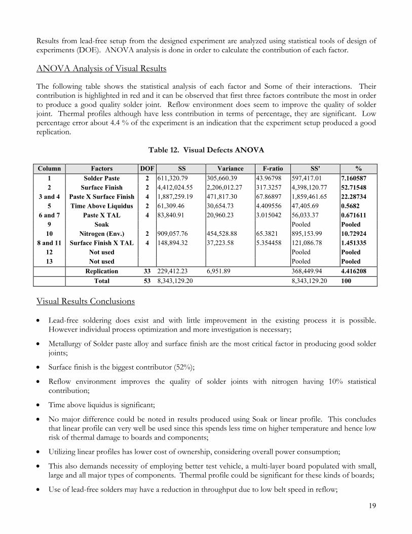
Results from lead-free setup from the designed experiment are analyzed using statistical tools of design of experiments (DOE). ANOVA analysis is done in order to calculate the contribution of each factor. ANOVA Analysis of Visual Results
The following table shows the statistical analysis of each factor and Some of their interactions. Their contribution is highlighted in red and it can be observed that first three factors contribute the most in order to produce a good quality solder joint. Reflow environment does seem to improve the quality of solder joint. Thermal profiles although have less contribution in terms of percentage, they are significant. Low percentage error about 4.4 % of the experiment is an indication that the experiment setup produced a good replication.
Table 12. Visual Defects ANOVA Column Factors DOF SS Variance F-ratio SS' %
1 Solder Paste 2 611,320.79 305,660.39 43.96798 597,417.01 7.160587 2 Surface Finish 2 4,412,024.55 2,206,012.27 317.3257 4,398,120.77 52.71548
3 and 4 Paste X Surface Finish 4 1,887,259.19 471,817.30 67.86897 1,859,461.65 22.28734 5 Time Above Liquidus 2 61,309.46 30,654.73 4.409556 47,405.69 0.5682
6 and 7 Paste X TAL 4 83,840.91 20,960.23 3.015042 56,033.37 0.671611 9 Soak Pooled Pooled
10 Nitrogen (Env.) 2 909,057.76 454,528.88 65.3821 895,153.99 10.72924 8 and 11 Surface Finish X TAL 4 148,894.32 37,223.58 5.354458 121,086.78 1.451335
12 Not used Pooled Pooled 13 Not used Pooled Pooled
Replication 33 229,412.23 6,951.89 368,449.94 4.416208 Total 53 8,343,129.20 8,343,129.20 100
Visual Results Conclusions
• Lead-free soldering does exist and with little improvement in the existing process it is possible. However individual process optimization and more investigation is necessary;
• Metallurgy of Solder paste alloy and surface finish are the most critical factor in producing good solder joints;
• Surface finish is the biggest contributor (52%);
• Reflow environment improves the quality of solder joints with nitrogen having 10% statistical contribution;
• Time above liquidus is significant;
• No major difference could be noted in results produced using Soak or linear profile. This concludes that linear profile can very well be used since this spends less time on higher temperature and hence low risk of thermal damage to boards and components;
• Utilizing linear profiles has lower cost of ownership, considering overall power consumption;
• This also demands necessity of employing better test vehicle, a multi-layer board populated with small, large and all major types of components. Thermal profile could be significant for these kinds of boards;
• Use of lead-free solders may have a reduction in throughput due to low belt speed in reflow;
20
• Higher temperature settings in the oven may be required. Likely overheads in implementation may not come from equipment but there may be added cost due to employee training for process changes;
• Components have to sustain higher and there is a need for major improvement in this area;
• None of the boards exhibited thermal damage to the FR4 laminate material; and
• Optimal settings:
Alloys: Sn/Ag and Sn/Ag/Cu Surface Finish: ENIG performs the best with these alloys. Profile: Linear profile TAL: 90 sec Reflow Environment: Nitrogen
CURRENT STATUS OF THE PROJECT
The visual defect tests are completed. The pull test fixture is designed and tested. The pull tests are being performed in UMass Lowell mechanical engineering lab. The reliability tests will be done at Raytheon reliability labs, and a second pull test will be performed after thermal cycling. Cross sectioning will be done for intermetallic growth. Publication of these results will be made in future conferences and will be available directly from the authors or TURI institute at UMASS Lowell. The Toxics Use Reduction Institute has a companion document to this report, entitled “Lead Free Soldering Process, Reliability and Options” authored by Shina and Belbase, which contains additional results and data associated with this study.
ACKNOWLEDGMENTS
The project team wishes to acknowledge the following for their knowledge, material and resource contributors to this research as well as the member corporations of the UMASS Lead Free Consortium
Liz Harriman, Toxics Use Reduction Institute Charles Pace, Center for Environmentally Appropriate Materials Raymond Lizotte, Texas Instruments BTU Corporation Multicore Solders Raytheon Company Sanmina (formerly Hadco) Corporation, Tech Center East Solectron, Massachusetts Corporation
We would like to thank Solectron Corporation, Westborough, MA site for assisting the project team in completing the final assembly of the boards at their facilities. Special thanks to Phil Provencal and entire staff of Solectron Massachusetts for their technical help and great moral support during the entire assembly process.
We would also like to Sanmina (formerly Hadco) Corporation for their contribution of the PWBs with the specified surface finishes. In particular Dennis Gagne of process engineering and General Manager Paul Nelson
Thanks to Raytheon Corporation Reliability Analysis Laboratory for their use of environmental chambers, and in particular; Bill Tice, Manager of the Laboratory.

21
SPONSORSHIP
This research was sponsored by The University Research in Sustainable Technologies program which is a joint project of the Toxics Use Reduction Institute (TURI) and the Center for Environmentally Appropriate Materials (CEAM) at University of Massachusetts Lowell, with support from the Commonwealth's STrategic Envirotechnology Partnership (STEP) program. The University Research program taps the research capabilities of the University of Massachusetts to advance the investigation, development and evaluation of sustainable technologies that are environmentally, occupationally and economically sound. The program provides research funding to UMass faculty from all campuses, annually, on a competitive basis and encourages faculty/industry partnerships and cross-campus collaboration.
REFERENCES
[1] IPC Roadmap 3rd Draft ( www.leadfree.org )
[2] Skidmore T. and Walters K., “Lead-Free Research: Optimizing Solder Joint Quality”, Circuit Assembly Magazine April 2000.
[3] Environmental Impacts of Toxicity of Lead Free Solders by Edwin B. Smith, KTEC Electronics.
[4] Proceedings: IPC Works '99
[5] Taguchi, G. System of Experimental Design, Genichi Vol 1. American Supplier Institute, 1989. p:\projects\urst\for web publication\shina\shina.doc