detector technology project international review committee...
TRANSCRIPT
DETECTOR TECHNOLOGY PROJECT INTERNATIONAL REVIEW
COMMITTEE 2013
December 10-11, 2013
SOI, MPGD, SCD, LiqTPC, FPIX, ASIC, CO2
KEK
Detector Technology Project
2
SOI PROJECT v.4 Dec. 6, 2013, Yasuo ARAI (KEK) (v.4b Jan. 30, 2014 minor correction)
Contents:
1. Introduction ..................................................................................................................... 3 2. SOI Pixel Process ........................................................................................................... 4
2.1 Wafer Process ........................................................................................................................................... 4 2.2 Back Gate Effect & BPW ......................................................................................................................... 5 2.3 Sensor Layers ........................................................................................................................................... 6 2.4 High Resistive Wafer ............................................................................................................................... 7 2.5 Leakage current ....................................................................................................................................... 9 2.6 Multi Project Wafer Run ..................................................................................................................... 10 2.7 Stitching ................................................................................................................................................. 11
3. Detector Developments ................................................................................................ 12 3.1 SEABAS Readout Board ........................................................................................................................ 12 3.2 Integration Type Pixel Detector (INTPIX) ........................................................................................... 13 3.3 X-ray Detector for Astrophysics (XRPIX) ............................................................................................. 15 3.4 XFEL Detector (SOPHIAS) ................................................................................................................... 17 3.5 Vertex Detector (PIXOR) ....................................................................................................................... 18 3.6 Low Temperature Applications ............................................................................................................. 19 3.7 Other Detector R&Ds ............................................................................................................................. 21
4. Advanced R&Ds ............................................................................................................ 23 4.1 Double SOI ............................................................................................................................................. 23 4.2 3D Vertical Integration .......................................................................................................................... 26
5. Data Base ..................................................................................................................... 29 5.1 Development History ............................................................................................................................. 29 5.2 Collaboration Members ......................................................................................................................... 29 5.3 Master Thesis ......................................................................................................................................... 32 5.4 Publications ............................................................................................................................................ 33 5.5 External Fundings ................................................................................................................................. 37 5.6 Patents .................................................................................................................................................... 37
6. References .................................................................................................................... 37

3
The Silicon-On-Insulator (SOI) pixel R&D [i] is targeting to develop monolithic pixel detectors for future high-energy physics experiments, X-ray experiments, and other applications. It integrates both radiation sensors and LSI circuits in one chip, and achieve high-resolution and intelligent detectors.
Fig. 1 shows the schematic view of the SOI pixel detector (SOIPIX). The SOI wafer is composed of a thick, high-resistivity substrate (sensor part) and a thin low-resistivity Si layer (CMOS circuitry) sandwiching a buried oxide (BOX) layer. After removing the top Si and the BOX layer in the region of the sensing node contacts, p or n dopant is implanted to the substrate. Then contact vias and metal connections from the p-n junction to the transistors are created. The main advantages of the SOI detectors are;
• There is no mechanical bump bonding, so obstacles, which will cause multiple scattering, are eliminated and smaller pixel size is possible.
• Parasitic capacitances of sensing nodes are very small (~10fF), so large conversion gain and low noise operation are possible.
• Full CMOS circuitry can be implemented in the pixel.
• The cross section of single event effects caused by radiation is very small. A latch-up mechanism, which destroys conventional bulk CMOS LSI, is absent.
• Unlike conventional CMOS process, there is no leakage path to bulk. Thus SOI transistors are shown to work over a very large temperature range from 4K to 600K.
• The technology is based on industry standards, and one of most promising technology for future LSIs. Thus further progress and lower cost are foreseeable.
• Emerging vertical (3D) integration techniques are a natural extension of the SOI technology, so a much higher integration density is possible.
We have started this R&D in 2005 by collaborating with Lapis Semiconductor Co. Ltd (see 5.1 Development History). Our process is developed based on their 0.2 µm CMOS fully-depleted (FD-) SOI process [ii].

4
Main specifications of the process are summarized in Table 1. We have been trying several kinds of high-resistivity wafers (CZ and FZ) for both n- and p-type wafers (see 2.4 High Resistive Wafer). To reduce development cost, we called academic sectors to join our MPW runs (see 2.6 Multi Project Wafer Run). The process has 5 layers of metal and can be implement MIM capacitor located on 3rd metal (Fig. 2) [iii].
Table 1. SOI pixel process specifications.
Process 0.2µm Low-Leakage Fully-Depleted SOI CMOS, 1 Poly, 5 Metal layers, MIM capacitor (1.5 fF/um2), DMOS option. Core (I/O) Voltage = 1.8 (3.3) V
SOI wafer Diameter: 200 mm!, Top Si: Cz, ~18 "-cm, p-type, ~40 nm thick Buried Oxide: 200 nm thick Handle wafer: 720 µm thick. Cz(n) ~ 700 "-cm, FZ(n) ~ 7k"-cm, FZ(p) ~ 25 k"-cm, etc.
Backside Thinned to 100 ~ 500 µm by mechanical grind, and chemical etching. Then adequate impurity is implant, laser Annealed, and Al is plated (200 nm).
Transistors Normal and low threshold transistors are available for both core and IO transistors. Three types of structures (body-floating, source-tie and body-tie) are available.
Optional process
Buried p-well formation Vertical integration with µ-bumps.
Fig. 1 Schematic view of the SOI Pixel Detector.
5
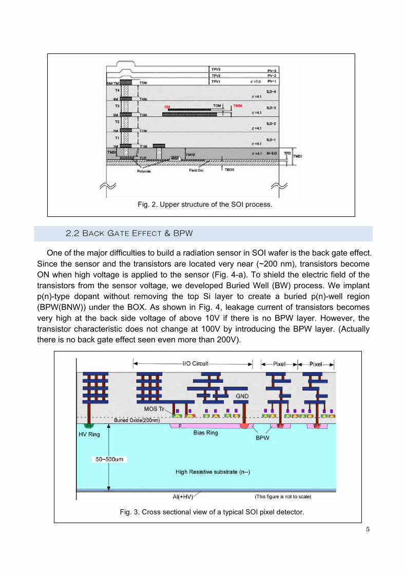
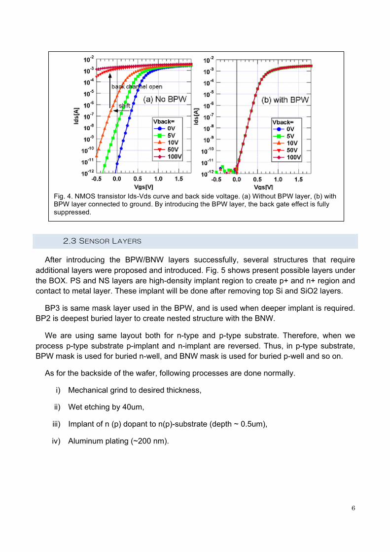
One of the major difficulties to build a radiation sensor in SOI wafer is the back gate effect. Since the sensor and the transistors are located very near (~200 nm), transistors become ON when high voltage is applied to the sensor (Fig. 4-a). To shield the electric field of the transistors from the sensor voltage, we developed Buried Well (BW) process. We implant p(n)-type dopant without removing the top Si layer to create a buried p(n)-well region (BPW(BNW)) under the BOX. As shown in Fig. 4, leakage current of transistors becomes very high at the back side voltage of above 10V if there is no BPW layer. However, the transistor characteristic does not change at 100V by introducing the BPW layer. (Actually there is no back gate effect seen even more than 200V).
Fig. 2. Upper structure of the SOI process.
Fig. 3. Cross sectional view of a typical SOI pixel detector.
6
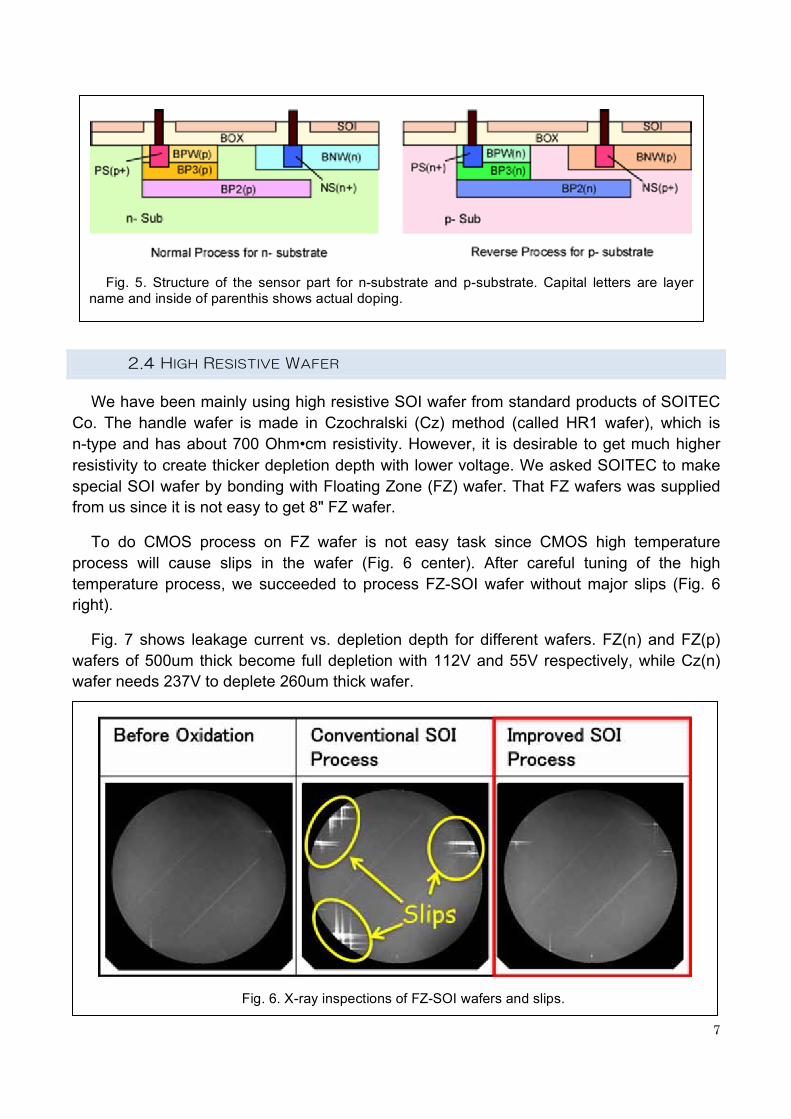
After introducing the BPW/BNW layers successfully, several structures that require additional layers were proposed and introduced. Fig. 5 shows present possible layers under the BOX. PS and NS layers are high-density implant region to create p+ and n+ region and contact to metal layer. These implant will be done after removing top Si and SiO2 layers.
BP3 is same mask layer used in the BPW, and is used when deeper implant is required. BP2 is deepest buried layer to create nested structure with the BNW.
We are using same layout both for n-type and p-type substrate. Therefore, when we process p-type substrate p-implant and n-implant are reversed. Thus, in p-type substrate, BPW mask is used for buried n-well, and BNW mask is used for buried p-well and so on.
As for the backside of the wafer, following processes are done normally.
i) Mechanical grind to desired thickness,
ii) Wet etching by 40um,
iii) Implant of n (p) dopant to n(p)-substrate (depth ~ 0.5um),
iv) Aluminum plating (~200 nm).
Fig. 4. NMOS transistor Ids-Vds curve and back side voltage. (a) Without BPW layer, (b) with BPW layer connected to ground. By introducing the BPW layer, the back gate effect is fully suppressed.
7
We have been mainly using high resistive SOI wafer from standard products of SOITEC Co. The handle wafer is made in Czochralski (Cz) method (called HR1 wafer), which is n-type and has about 700 Ohm•cm resistivity. However, it is desirable to get much higher resistivity to create thicker depletion depth with lower voltage. We asked SOITEC to make special SOI wafer by bonding with Floating Zone (FZ) wafer. That FZ wafers was supplied from us since it is not easy to get 8" FZ wafer.
To do CMOS process on FZ wafer is not easy task since CMOS high temperature process will cause slips in the wafer (Fig. 6 center). After careful tuning of the high temperature process, we succeeded to process FZ-SOI wafer without major slips (Fig. 6 right).
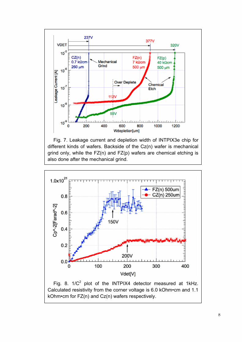
Fig. 7 shows leakage current vs. depletion depth for different wafers. FZ(n) and FZ(p) wafers of 500um thick become full depletion with 112V and 55V respectively, while Cz(n) wafer needs 237V to deplete 260um thick wafer.
Fig. 5. Structure of the sensor part for n-substrate and p-substrate. Capital letters are layer name and inside of parenthis shows actual doping.
Fig. 6. X-ray inspections of FZ-SOI wafers and slips.
8
Fig. 7. Leakage current and depletion width of INTPIX3e chip for different kinds of wafers. Backside of the Cz(n) wafer is mechanical grind only, while the FZ(n) and FZ(p) wafers are chemical etching is also done after the mechanical grind.
Fig. 8. 1/C2 plot of the INTPIX4 detector measured at 1kHz. Calculated resistivity from the corner voltage is 6.0 kOhm•cm and 1.1 kOhm•cm for FZ(n) and Cz(n) wafers respectively.
9
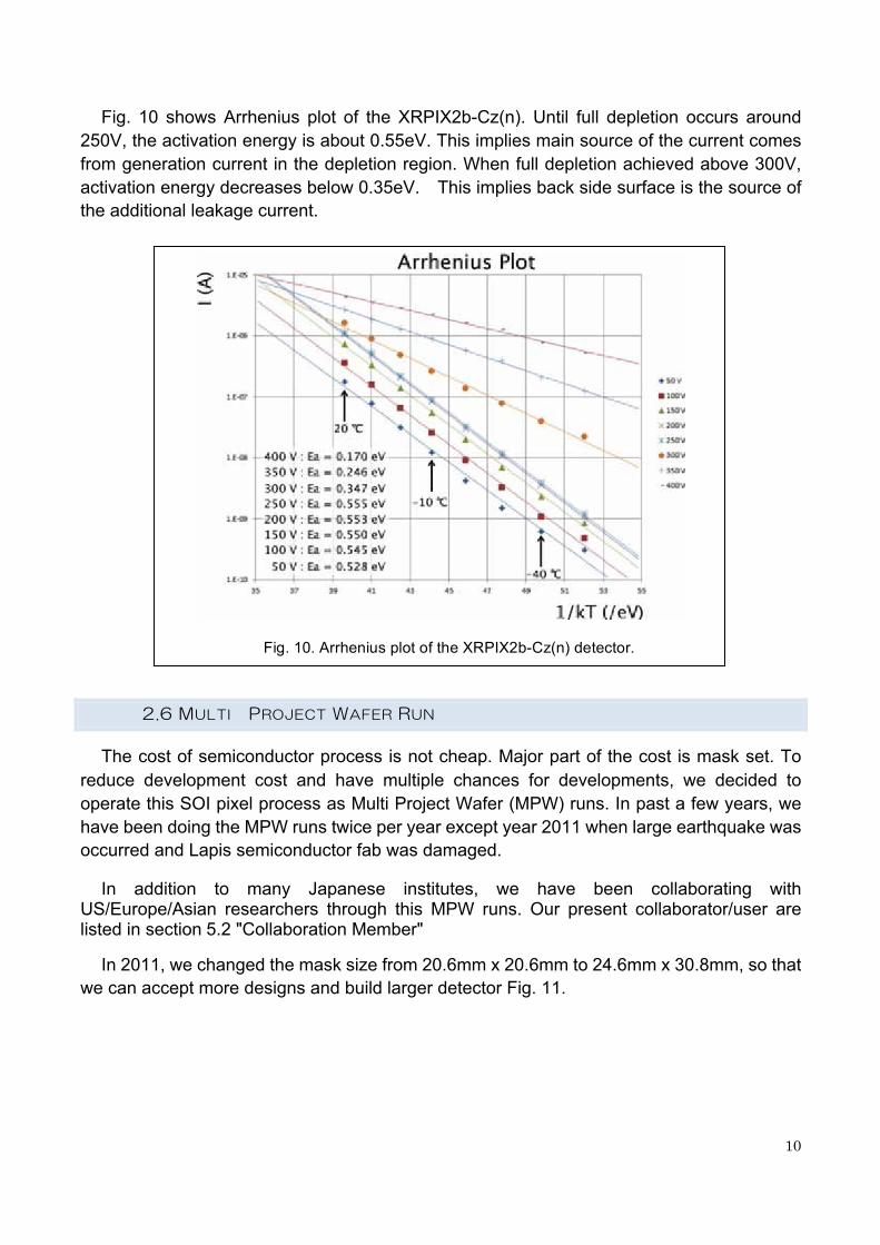
While leakage current of the sensor is not so important for short integration time applications, it is important for long integration time applications such as astronomical X-ray observation and measurements that require good energy resolution.
Table 2 shows leakage current of a few detectors. CZ(n)(=HR1) wafer shows relatively large leakage current (> 100nA/cm2@Room Temp.), while FZ(n) wafer shows better leakage current (10nA/cm2@20ºC). Fig. 9 shows temperature dependence of the XRPIX1 leakage current. By lowering temperature, leakage current will decrease but become constant below -20 ºC. We have not yet identified the source of the constant leak curent.
Table 2. Summary of leakage current @Vdet=10V.
Chip/TEG Wafer Temp. Leakage current XRPIX1 Cz(n) 25 ºC 440 nA/cm2 XRPIX1 Cz(n) -50 ºC 0.3 nA/cm2 XRPIX1 FZ(n) 20 ºC 10 nA/cm2 XRPIX1 FZ(n) -20 ºC 0.1 nA/cm2 MAMBO IV (nested well) FZ(n) Room T <100 nA/cm2 INTPIX/CNTPIX Cz(n) Room T 100~300 nA/cm2
Fig. 9. Dark Current of the XRPIX1 FZ-SOI. Pixel size is 30.6 um square. Target spec is 2pA/cm2.
10
Fig. 10 shows Arrhenius plot of the XRPIX2b-Cz(n). Until full depletion occurs around 250V, the activation energy is about 0.55eV. This implies main source of the current comes from generation current in the depletion region. When full depletion achieved above 300V, activation energy decreases below 0.35eV. This implies back side surface is the source of the additional leakage current.
The cost of semiconductor process is not cheap. Major part of the cost is mask set. To reduce development cost and have multiple chances for developments, we decided to operate this SOI pixel process as Multi Project Wafer (MPW) runs. In past a few years, we have been doing the MPW runs twice per year except year 2011 when large earthquake was occurred and Lapis semiconductor fab was damaged.
In addition to many Japanese institutes, we have been collaborating with US/Europe/Asian researchers through this MPW runs. Our present collaborator/user are listed in section 5.2 "Collaboration Member"
In 2011, we changed the mask size from 20.6mm x 20.6mm to 24.6mm x 30.8mm, so that we can accept more designs and build larger detector Fig. 11.
Fig. 10. Arrhenius plot of the XRPIX2b-Cz(n) detector.
11
Large area detectors are often required in some experiments, but the mask size is limited to 24.6mm x 30.8mm in size. Therefore, we have developed stitching technique to make large format detector by using only one mask set. Fig. 12 shows the stitching method and photographs of the processed wafer.
The development is mainly driven by Riken group for the SOPHIAS detector. Since this was our first trial, we took buffer region size of 10um and connect only minimum number of layers (PS, NS and metal 1). However, Lapis is confident to make buffer region shorter and connects all metals.
Fig. 11.. Examples of Mask layouts. (Left) FY2010 : 20.6mm x 20.6mm.
12
There are many activities of detector developments using the SOI pixel process. In this section, we flash major activities of the developments.
To test manufactured chip quickly, we have developed SEABAS (SOI EvAluation BoArd with Sitcp) read out board. The board contains two FPGAs one for controlling the SOI pixel and the other is for transferring the data through Ethernet (called SiTCP).
Fig. 13 and Fig. 14 show block diagram and photograph of the SEABAS2 (2nd generation board) respectively. By using the SEABAS2 board, we could take ~70 frame/sec with INTPIX4 detector (425k pixels).
Fig. 12. Stitching exposure for the SOPHIAS detector. Both edge structure and pixel structure were drawn in a mask. Part of the mask is blocked during exposure. In this detector (SOPHIAS), pixel layout was repeated 3 times and edge structures are exposed at both ends.
13
Main SOI detectors developed so far are integration-type pixel detectors. The basic schematic of the sensor and a layout are shown in Fig. 15. The circuit is similar to that of the CMOS optical imager. Smallest size of the pixel we have developed is 8 µm square. Many of the integration-type pixels have correlated double sampling (CDS) circuit in each pixel or in column circuit. Largest chip (INTPIX5/6) so far tested has 896 x 1408 (~1.3 M) pixels, and new chip (INTPIX7) under process has 1408 x 1408 (~2M) pixels. Specifications of major integration-type detector are summarized in Table 3.
An example of X-ray image taken by the INTPIX4 detector is shown in Fig. 16.
Fig. 13. Block diagram of the SEABAS2..
Fig. 14, Photograph of the SEABAS2 board and the INTPIX4 sub-board.
14
Table 3. Specification of major integration-type pixel detectors.
DIPIX1/2 FPIX1 INTPIX4 INTPIX5/6 INTPIX7 (under process)
Pixel Size [um] 14 x 14 8 x 8 17 x 17 12 x 12 12 x 12 Chip Size [mm] 5 x 5 6 x 6 10.2 x 15.4 12.2 x 18.4 18.4 x 18.4 BPW width [um] 10 6 12 9 9 CDS Pixel CDS - Pixel CDS Column CDS Pixel CDS Store Switch O - O O O
Wafer n or p n and p n n and p (INT5) n or p (INT6N or P) p (Double SOI)
Gain Fix (9.3 uV/e-)
Fix (~28 uV/e-)
Fix (12.6 uV/e-)
2 gain (~16 or 2.5 uV/e-) Fix
Max. Charge ~110 ke- ~40 ke- 80 ke- ~70 or 460 ke- -
No. of Pixels 256 x 128 x 2 (~65 kpix)
512 x 512 (~260 kpix
512 x 832 ~430 kpix
896 x 1408 (~1,260 kpix
1408 x 1408 (~1,982 kpix
No. of Output 1 1 or 9 1 or 13 1 or 11 1 or 11 Rolling Shutter - O - O O
Fig. 15. (Left) A typical circuit schematic of the integration-type pixel with CDS function. (Right) Layout of INTPIX7 pixel. The size of the pixel is 12um x 12um.
15
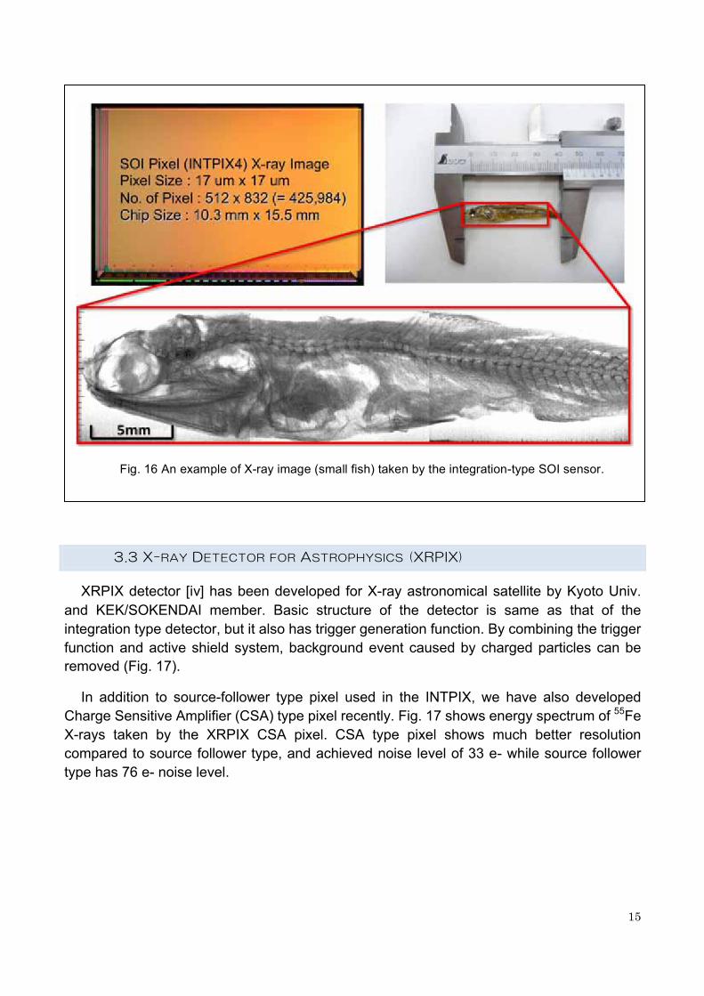
XRPIX detector [iv] has been developed for X-ray astronomical satellite by Kyoto Univ. and KEK/SOKENDAI member. Basic structure of the detector is same as that of the integration type detector, but it also has trigger generation function. By combining the trigger function and active shield system, background event caused by charged particles can be removed (Fig. 17).
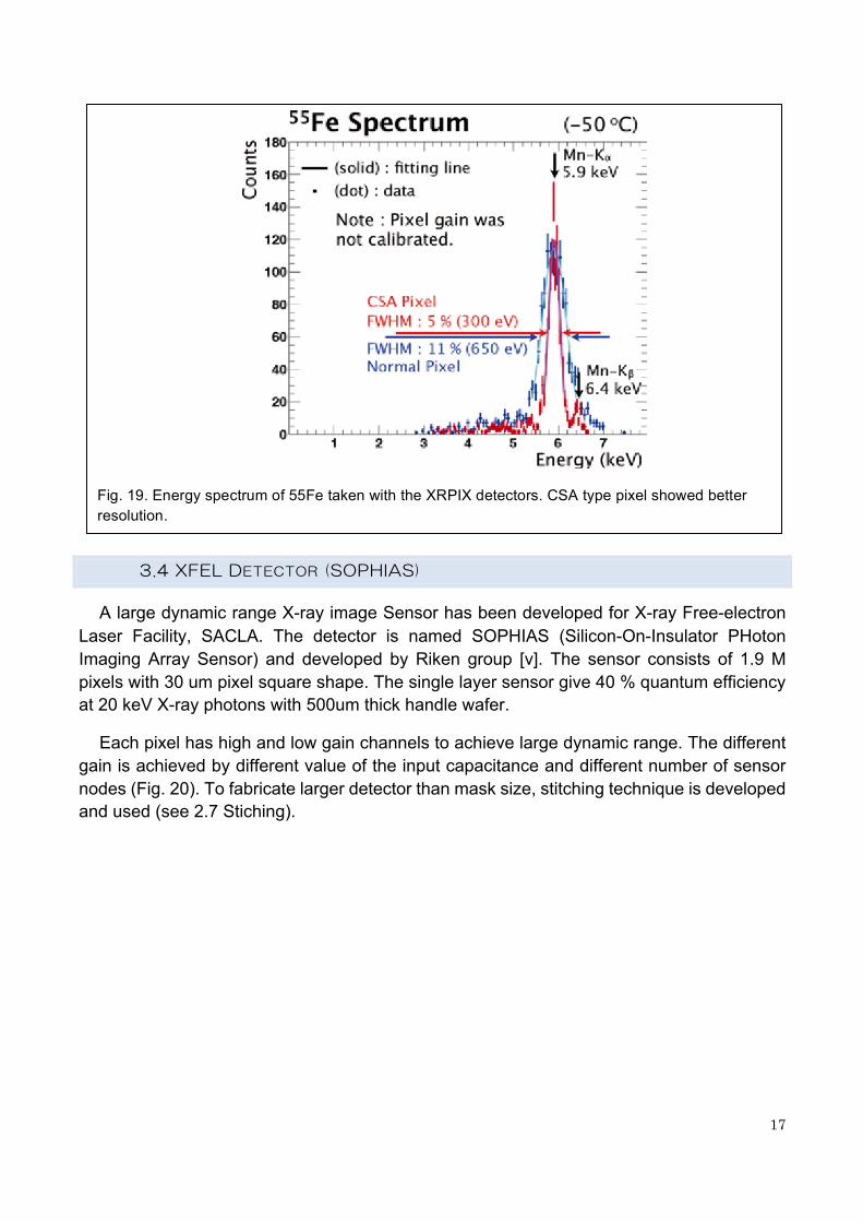
In addition to source-follower type pixel used in the INTPIX, we have also developed Charge Sensitive Amplifier (CSA) type pixel recently. Fig. 17 shows energy spectrum of 55Fe X-rays taken by the XRPIX CSA pixel. CSA type pixel shows much better resolution compared to source follower type, and achieved noise level of 33 e- while source follower type has 76 e- noise level.
Fig. 16 An example of X-ray image (small fish) taken by the integration-type SOI sensor.
16
Fig. 17 Concept of an active shield system with the XRPIX. Non-X-ray background can be rejected by anti-coincidence with the active shield (scintillation counters).
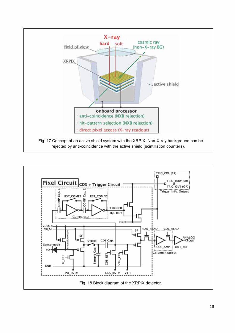
Fig. 18 Block diagram of the XRPIX detector.
17
A large dynamic range X-ray image Sensor has been developed for X-ray Free-electron Laser Facility, SACLA. The detector is named SOPHIAS (Silicon-On-Insulator PHoton Imaging Array Sensor) and developed by Riken group [v]. The sensor consists of 1.9 M pixels with 30 um pixel square shape. The single layer sensor give 40 % quantum efficiency at 20 keV X-ray photons with 500um thick handle wafer.
Each pixel has high and low gain channels to achieve large dynamic range. The different gain is achieved by different value of the input capacitance and different number of sensor nodes (Fig. 20). To fabricate larger detector than mask size, stitching technique is developed and used (see 2.7 Stiching).
Fig. 19. Energy spectrum of 55Fe taken with the XRPIX detectors. CSA type pixel showed better resolution.

18
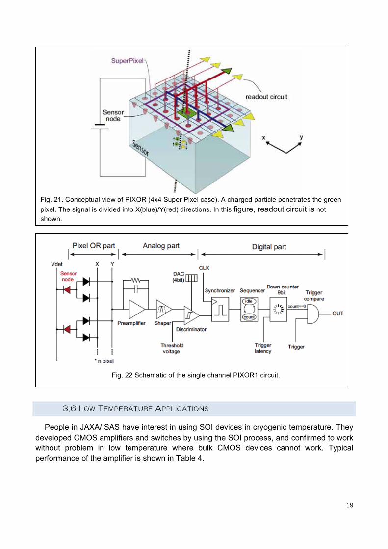
As an R&D for future vertex detector for Belle II experiment, a new detector PIXOR (PIXel OR) is being developed by Tohoku Univ. group [vi]. An analog signal from each pixelated sensor is divided into two-dimensional directions, and 2N signal channels from a small N-by-N pixel matrix are ORed as N column and N row channels (Fig. 21). Then the signals are processed by a readout circuit in each small matrix and wait for a trigger (Fig. 22).
This PIXOR scheme reduces the number of readout channels and avoids a deterioration of intrinsic position resolution due to large circuit area that was a common issue for monolithic detectors. This feature allows high resolution, low occupancy and on-sensor signal processing at the same time.
Fig. 20. Outlook of the SOPHIAS detector and schematics of the pixel.
19
People in JAXA/ISAS have interest in using SOI devices in cryogenic temperature. They developed CMOS amplifiers and switches by using the SOI process, and confirmed to work without problem in low temperature where bulk CMOS devices cannot work. Typical performance of the amplifier is shown in Table 4.
Fig. 21. Conceptual view of PIXOR (4x4 Super Pixel case). A charged particle penetrates the green pixel. The signal is divided into X(blue)/Y(red) directions. In this figure, readout circuit is not shown.
Fig. 22 Schematic of the single channel PIXOR1 circuit.
20
Table 4. Performance of FD-SOI CMOS amplifier at 4.2K.
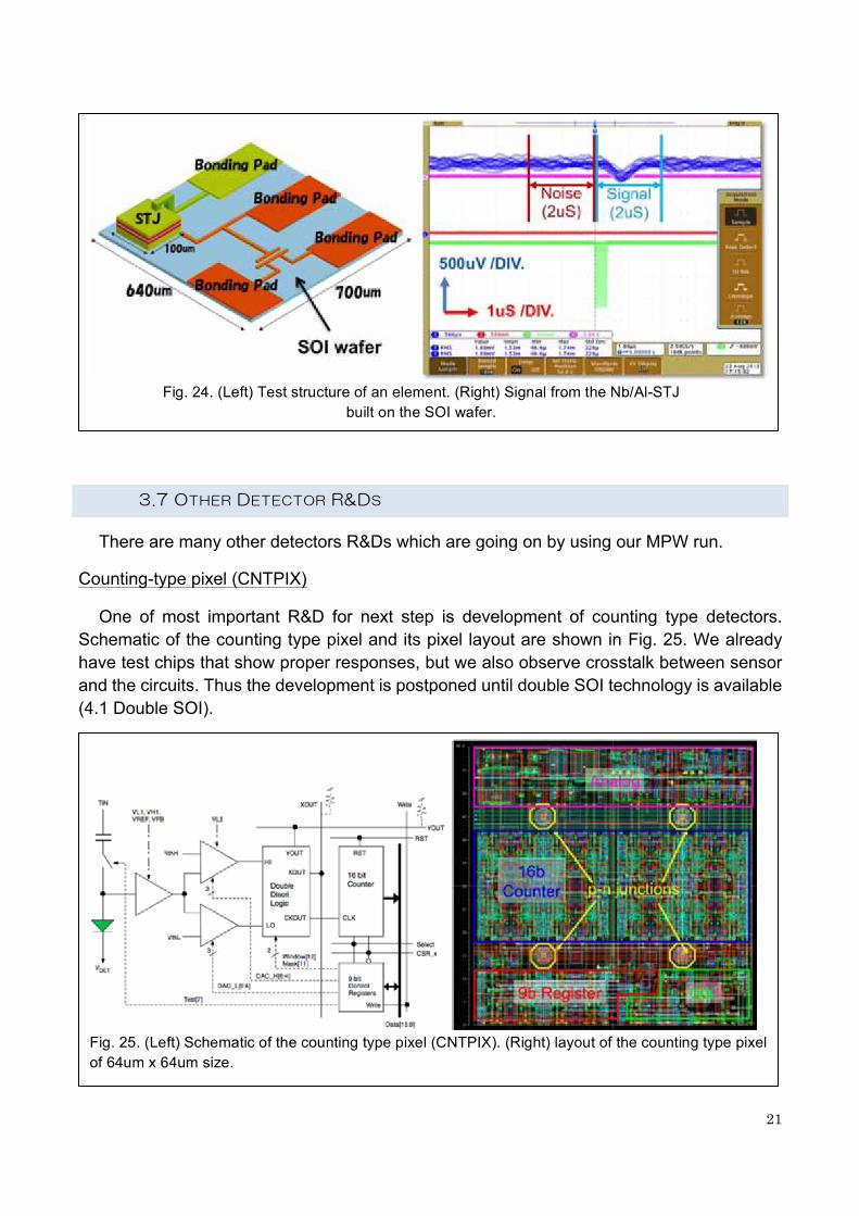
After the success of the cryogenic operation, we started a project to build Superconducting Tunnel Junction (STJ) devices on processed SOI wafer with Univ. of Tsukuba group. When we want to arrange the STJ devices in array, extraction of STJ signals to room temperature is always annoying issue. If we succeed to build the STJ on processed SOI wafer and make good connections between them, number of the connection can be greatly reduced and S/N can be improved.
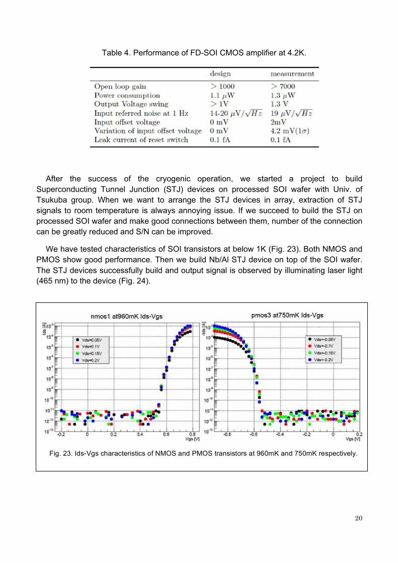
We have tested characteristics of SOI transistors at below 1K (Fig. 23). Both NMOS and PMOS show good performance. Then we build Nb/Al STJ device on top of the SOI wafer. The STJ devices successfully build and output signal is observed by illuminating laser light (465 nm) to the device (Fig. 24).
Fig. 23. Ids-Vgs characteristics of NMOS and PMOS transistors at 960mK and 750mK respectively.
21
There are many other detectors R&Ds which are going on by using our MPW run.
Counting-type pixel (CNTPIX)
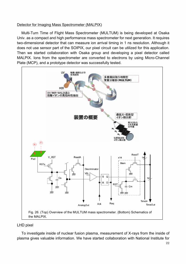
One of most important R&D for next step is development of counting type detectors. Schematic of the counting type pixel and its pixel layout are shown in Fig. 25. We already have test chips that show proper responses, but we also observe crosstalk between sensor and the circuits. Thus the development is postponed until double SOI technology is available (4.1 Double SOI).
Fig. 24. (Left) Test structure of an element. (Right) Signal from the Nb/Al-STJ
built on the SOI wafer.
Fig. 25. (Left) Schematic of the counting type pixel (CNTPIX). (Right) layout of the counting type pixel of 64um x 64um size.
22
Detector for Imaging Mass Spectrometer (MALPIX)
Multi-Turn Time of Flight Mass Spectrometer (MULTUM) is being developed at Osaka Univ. as a compact and high performance mass spectrometer for next generation. It requires two-dimensional detector that can measure ion arrival timing in 1 ns resolution. Although it does not use sensor part of the SOIPIX, our pixel circuit can be utilized for this application. Then we started collaboration with Osaka group and developing a pixel detector called MALPIX. Ions from the spectrometer are converted to electrons by using Micro-Channel Plate (MCP), and a prototype detector was successfully tested.
LHD pixel
To investigate inside of nuclear fusion plasma, measurement of X-rays from the inside of plasma gives valuable information. We have started collaboration with National Institute for
Fig. 26. (Top) Overview of the MULTUM mass spectrometer. (Bottom) Schematics of the MALPIX.

23
Fusion Science (NIFS) for measurement of Large Helical Device (LHD). First test is scheduled on Dec. 2013.
TDI pixel
X-ray detectors are used widely in many kinds of inspection system. Especially to find small metallic debris of ~10um size within battery has crucial demand in future electrical vehicles and so on. To find such small debris from materials on high-speed belt conveyor, SOIPIX is very suitable with its high resolution. However, to receive enough X-rays from moving object, Time Delayed Integration (TDI) method is mandatory. Although it is easy to implement the TDI in CCD device, it is difficult to do in CMOS device. We have invented a new method to implement digital TDI in the SOIPIX.
RADPIX
After the accident of the Fukushima nuclear power plant, people become very sensitive to radiations. Although SOIPIX does not have high efficiency for a few hundreds keV gamma rays, pixelated sensor has advantage to identify type of the radiation and detection of alpha and beta rays. Thus we are developing a pixel detector (RADPIX) for monitoring environmental radiation. It includes leakage current compensation circuit for continuous detection of radiation.
While we solved the back gate problem by introducing BPW layer, there still remain two issues to make the SOIPIX used widely.
• Crosstalk between sensor node and circuit,
• Radiation tolerance of the detector.
The crosstalk generates unwanted signals and makes operation of the detector unstable. While the SOI is immune to Single Event Effect (SEE), it is not so rad-hard to Total Ionization Dose (TID) due to the BOX and surrounding oxide. Tolerable radiation level of present SOIPIX devices is about 2 kGy, and many applications require more than 10 kGy (1 Mrad) tolerance.
After all, to solve these issues, we need another conduction layer between sensor and circuit. We asked SOITEC to make double SOI wafer which has two sets of thin Si and BOX pair layers. General view of the double SOI pixel detector is shown in Fig. 27, and cross section of processed double SOI wafer is shown in Fig. 28. In addition to above two issues, the newly introduced middle Si layer (SOI2) shields back gate effect too (Fig. 29), so that we can optimize the size of the BPW without considering the back gate effect.
24
The first double SOI wafers were produced by SOITEC Co. with n-substrate, but second DSOI wafers have been produced by Shin-Etsu Chemical Co. Ltd, Japan, with p-type substrate.
When we irradiate gamma rays to the SOI, transistor threshold voltage will move to negative direction (Fig. 29 left) due to hole trapping in the oxide. However, by applying negative voltage to the middle Si, electric field generated by the hole is compensated and the threshold voltage will return to almost original value (Fig. 30).
Fig. 27. General view of the pixel detector using the double SOI wafer.
Fig. 28. Cross sectional view of the double SOI wafer. In addition to top SOI and substrate, we introduced middle SOI layer. (Unfortunately, the contact to the middle Si is out of the photograph.)
25
Fig. 31 plots optimum value of the SOI2 layer to return the threshold value to original value [vii]. The statistics of the data is not yet enough and there is large variation in the data of NMOS core transistors. However we can see the optimum value for dose up to 20 kGy looks same for all the transistors. On the other hand, at above 20 kGy, we see some rebound in
Fig. 29. Back gate effect suppression by the middle Si. (Left) Middle Si is floating. (Right) Middle Si
is connected to ground and the back gate effect is fully suppressed.
Fig. 30. Id-Vgs curve change with g-ray irradiation and middle Si voltage (VSOI2). (Top) NMOS, (Bottom) PMOS.

26
NMOS transistors. Then we may need to separate the SOI2 layer between NMOS and PMOS for the application that requires more than 20 kGy radiation tolerance.
Although the SOI detector is successfully being developed, future pixel detectors such as used in the International Linear Collider (ILC) requires much more transistors to implement memories and data processing logics than available today. Since the readout circuit needs analog amplification circuits etc., it is not necessary good to go fine node process.
If we try to implement such memory and logics inside the pixel, the pixel size must be very large (> 60 x 60 um2), while the experiment requires smaller pixel size less than 20 x 20 um2. To solve this, we have started R&D of 3D vertical integration by using µ-bump technology [viii] in collaboration with T-Micro Co.
Fig. 32 shows the process flow of the vertical stacking of circuit layers. Base SOI chips as upper and lower tiers are fabricated in a SOI wafer. Minimum bump pad opening size is 3 µm x 3 µm. After forming under bump metallization (UBM), Indium bumps are formed using
Fig. 31. Optimum SOI2 value to return threshold for various kinds of transistors. Both 'NMOS and PMOS' and 'Core and IO' transistors are showing similar tendency.
27
evaporation and lift-off technique. The minimum bump size and pitch are 2.5-µm sq. and 5 µm respectively.
Lower tier and upper tier are aligned using IR microscope. Initial alignment error before welding bumps must be kept less than 1.0 µm in order to obtain stable electrical connection. After fusing into one connection, the tiers are self-aligned to less than 0.6 µm. The gap between tiers is about 1.5 µm. An array of Indium µ-bump junctions does not have enough mechanical strength. So combining gap fill with adhesive is indispensable and injection method is the key of this process.
Fig. 33 shows layout of alignment mark and photographs of the alignment marks at 4 corners after the bonding and the adhesive injection. The chips are aligned at better than 1 um accuracy. Since the space between tiers is not uniform due to unbalance distribution of the µ-bumps in the chip, adhesive injection caused voids at the points where rapid pressure loss occurs. White island area seen in Fig. 33-bottom upper left photo is such a void. Number of the voids is greatly reduced by controlling differential pressure assisted capillary action. Although we are bonding chip to chip in this study, chip to wafer bonding techniques are also being developed for mass production.
Fig. 32. Process flow for the stack process with micro bump technology.
28
Fig. 33. (Top) Alignment mark size, (Bottom) Alignment of upper and lower chips after stacking.
29
2005. 5 Propose SOI Pixel R&D to KEK Detector Technology Project 2005. 7 Start Collaboration with OKI Electronics Co. Ltd. 2005.10 First submission to Univ. of Tokyo (VDEC) 0.15µm SOI MPW run. 2006.12 First MPW run of 0.15um SOI process operated by KEK. 2007.3 First SOI Workshop @KEK 2007. 6 Process change to Miyagi 0.2um line due to discontinue of Hachioji 0.15 µm line. 2007.10 First User Meeting @U. of Hawaii (IEEE NSS) 2008. 1 First MPW run of 0.2µm SOI process. 2008.3 SOI Workshop @KEK 2008.10 OKI semiconductor division was spin-off to OKI semiconductor Co. Ltd, and enters
under Rohm Co. group. 2009. 1 Metal Pitch is shrunken from 0.88um to 0.58um.
Introduce Buried P-Well structure. 2009.2 SOI W.S. @Kyoto Univ. 2010.3 Collab. Mtg. @Fermilab 2011.2 International Review @KEK 2011.3 OKI Semi Miyagi Fab. was damaged by the large earthquake. 2011.9 Name of OKI Semi was changed to Lapis Semiconductor Co. Ltd. 2011.10 Mask size was increased from 20.6 mm square to 24.6 mm x 30.8 mm. 2012.3 Collab. Mtg. @LBNL 2012.8 First double SOI wafer was processed. 2012.9 PIXEL2012 conference @Fukushima. 2013.2 Mini Workshop @IHEP (China) 2013.5 Collab. Mtg. @Krakow (AGH & IFJ) 2013.8 10th 0.2um MPW run was submitted.
[Japanese Members]
Name Affiliation Koichi NAGASE JAXA/ISAS Hirokazu Ikeda JAXA/ISAS Testuichi Kishishita JAXA/ISAS Daisuke Kobayashi JAXA/ISAS Takehiko WADA JAXA/ISAS Ryuichi Takashima Kyoto Univ. of Education Shou Moritake Kyoto Univ. of Education Shinya Nakashima Kyoto Univ. Hironori Matsumoto Nagoya Univ. Syukyo G. Ryu Kyoto Univ. Takeshi Tsuru Kyoto Univ. Takaaki Tanaka Kyoto Univ. Hideaki Matsumura Kyoto Univ.
30
Jiro Ida Kanazawa Institute of Technology Kazuya Tauchi KEK, High Energy Accelerator Research Organization Ryo Ichimiya KEK, High Energy Accelerator Research Organization Susumu Terada KEK, High Energy Accelerator Research Organization Takashi Kohriki KEK, High Energy Accelerator Research Organization Tomohisa Uchida KEK, High Energy Accelerator Research Organization Toru Tsuboyama KEK, High Energy Accelerator Research Organization Toshinobu Miyoshi KEK, High Energy Accelerator Research Organization Yasuo Arai KEK, High Energy Accelerator Research Organization Yoichi Ikegami KEK, High Energy Accelerator Research Organization Yoshinobu Unno KEK, High Energy Accelerator Research Organization Yowichi Fujita KEK, High Energy Accelerator Research Organization Yukiko Ikemoto KEK, High Energy Accelerator Research Organization Shingo Mitsui KEK, High Energy Accelerator Research Organization Motohiko Omodani JASRI, XFEL division Takashi Kameshima JASRI, XFEL division Hirofumi Tadokoro National Institute of Advanced Industrial Science and Technology Masashi Yanagihara National Institute of Advanced Industrial Science and Technology Morifumi Ohno National Institute of Advanced Industrial Science and Technology Yasushi Igarashi National Institute of Advanced Industrial Science and Technology Hidehiko Nakaya National Astronomical Observatory of Japan
Ayaki Takeda The Graduate University for Advanced Studies School of High Energy Accelerator
Daisuke Nio The Graduate University for Advanced Studies School of High Energy Accelerator Science
Kazunori Hanagaki Department of Physics, Osaka Univ. Minoru Hirose Department of Physics, Osaka Univ. Toshihiro Idehara Department of Physics, Osaka Univ. Kazuhiko Hara Univ. of Tsukuba, Faculty of Pure and Applied Sciences Yuji Takeuchi Univ. of Tsukuba, Faculty of Pure and Applied Sciences Shinhong Kim Univ. of Tsukuba, Faculty of Pure and Applied Sciences Mari Asano Univ. of Tsukuba, Graduate School of Pure and Applied Sciences Naoshi Tobita Univ. of Tsukuba, Graduate School of Pure and Applied Sciences Tatsuya Maeda Univ. of Tsukuba, Graduate School of Pure and Applied Sciences Kouhei Tsuchida Univ. of Tsukuba, Graduate School of Pure and Applied Sciences Shunsuke Honda Univ. of Tsukuba, Graduate School of Pure and Applied Sciences Kouta Kasahara Univ. of Tsukuba, Graduate School of Pure and Applied Sciences Kouhei Shinsho Univ. of Tsukuba, Graduate School of Pure and Applied Sciences Yoshiyuki Onuki Univ.of Tokyo Hideki Hamagaki Univ.of Tokyo Yuuko Sekiguchi Univ.of Tokyo Hitoshi Yamamoto Tohoku Univ. Akimasa Ishikawa Tohoku Univ. Yutaro Sato Tohoku Univ. Hironori Katsurayama Tohoku Univ. Shinoda Naoyuki Tohoku Univ. Yoshimasa Ono Tohoku Univ. Kouji Mori Miyazaki Univ. Yuusuke Nishioka Miyazaki Univ. Kazuo Kobayashi RIKEN, RIKEN SPring-8 Center Shun Ono RIKEN, RIKEN SPring-8 Center Takaki Hatsui RIKEN, RIKEN SPring-8 Center Tougo Kudo RIKEN, RIKEN SPring-8 Center Kameshima Takashi RIKEN, RIKEN SPring-8 Center Yoichi Kirihara RIKEN, RIKEN SPring-8 Center

31
Sadatsugu Muto National Institute for Fusion Science Shigeru Sudo National Institute for Fusion Science Naoki Tamura National Institute for Fusion Science Yasuhiko Ito National Institute for Fusion Science Hideya Nakanishi National Institute for Fusion Science Tsukada Kiwamu Nagoya Institute of Technology Masayuki Ikebe Hokkaido Univ. Shoji Kawahito Shizuoka Univ. Keiichiro Kagawa Shizuoka Univ. Keita Yasutomi Shizuoka Univ. Takeo Watanabe Univ. of Hyogo Nobukazu Teranishi Univ. of Hyogo
[Foreign Members]
Name Affiliation Chih Hsun Lin Academia Sinica, Taiwan Minglee Chu Academia Sinica, Taiwan
Sebastian Glab Department of Electronics AGH-University of Science and Technology (AGH-UST)
Wojciech Kucewicz Department of Electronics AGH-University of Science and Technology (AGH-UST)
Marek Idzik Krakow's University of Science and Technology (AGH-UST) Mohammed Imran Ahmed Institute of Nuclear Physics, Krakow Piotr Kapusta Institute of Nuclear Physics, Krakow Farah Khalid Fermilab Grzegorz Deptuch Fermilab Marcel Trimpl Fermilab Raymond Yarema Fermilab Ronald Lipton Fermilab Ivan Peric Institut für Technische Informatik der Universität Heidelberg Peter Fischer Institut für Technische Informatik der Universität Heidelberg Lei Fan Institute of High Energy Physics, Chinese Academy of Sciences Liu Gang Institute of High Energy Physics, Chinese Academy of Sciences Xiaoshan JIANG Institute of High Energy Physics, Chinese Academy of Sciences Yunpeng Lu Institute of High Energy Physics, Chinese Academy of Sciences Zheng Wang Institute of High Energy Physics, Chinese Academy of Sciences Yi Liu Institute of High Energy Physics, Chinese Academy of Sciences
Qi Zhang Shanghai Advanced Research Institute, Chinese Academy of Sciences. (SARI, CAS)
Ning Wang Shanghai Advanced Research Institute, Chinese Academy of Sciences. (SARI, CAS)
Tian Li Shanghai Advanced Research Institute, Chinese Academy of Sciences. (SARI, CAS)
Hui Wang Shanghai Advanced Research Institute, Chinese Academy of Sciences. (SARI, CAS)
Qi Zhang Shanghai Advanced Research Institute, Chinese Academy of Sciences. (SARI, CAS)
Zhao Kai The Institute of Microelectronics of the Chinese Academy of Sciences (IMECAS)
Chinh Vu LBNL Devis Contarato LBNL Lindsay Glesener LBNL Peter Denes LBNL
32
Craig S Tindall LBNL Marco Battaglia LBNL, UC Santa Cruz Eduardo Cortina Louvain-la-Neuve University Elena Martin Universitat Autonoma de Barcelona Lawrence Soungyee Louvain-la-Neuve University Paula liliana alvarez rengifo Louvain-la-Neuve University
Gary Varner Univ. of Hawaii Michael Cooney Univ. of Hawaii Angel Dieguez University of Barcelona Dario Bisello University of Padova & INFN Padova, Italy Devis Pantano University of Padova & INFN Padova, Italy Serena Mattiazzo University of Padova & INFN Padova, Italy Piero Giubilato University of Padova and INFN Padova, Italy, & LBNL, USA
[Cooperation Companies]
Name Lapis Semiconductor Co. Ltd. Lapis Semiconductor Miyagi Co. Ltd. A-R-Tec Co. Rigaku Co. T-micro Co. Ltd. REPIC Co. Ltd. Digian Technology Inc.
33
[English] 1 "Hard X-Ray SOI Sensor Prototype", E. Martin, G. Varner, M. Barbero, J. Kennedy, H. Tajima, Y. Arai,
IEEE Ph. D. Research in Microelectronics and Electronics, 11 - 16 June 2006, Otranto (Lecce), Italy 2 "First Results of 0.15um CMOS SOI Pixel Detector", Y. Arai, M. Hazumi, Y. Ikegami, T. Kohriki, O. Tajima,
S. Terada, T. Tsuboyama, Y. Unno, H. Ushiroda, H. Ikeda, K. Hara, H. Ishino, T. Kawasaki, E. Martin, G. Varner, H. Tajima, M. Ohno, K. Fukuda, H. Komatsubara, J. Ida, SNIC Symposium, Stanford, California, 3-6 April 2006, SLAC-PUB-12079, KEK preprint, 2006-34, SLAC Electronic Conference Proceedings Archive (SLAC-R-842, eConf: C0604032) PSN-0016. http://www.slac.stanford.edu/econf/C0604032/papers/0016.PDF.
3 "Monolithic Pixel Detector in a 0.15mm FD-SOI Technology", Y. Arai,presented at the 6th Hiroshima symposium of Development and Application of semiconductor tracking devices, Sep. 11-15, 2006, Carmel, California, U.S.A.
4 "Development of a CMOS SOI Pixel Detector", Y. Arai, M. Hazumi, Y. Ikegami, T. Kohriki, O. Tajima, S. Terada T. Tsuboyama, Y. Unno, Y. Ushiroda, H. Ikeda, K. Hara, H. Ishino, T. Kawasaki, H. Miyake, E. Martin, G. Varner, H. Tajima M. Ohno, K. Fukuda, H. Komatsubara, J. Ida,Proceedings of 12th Workshop on Electronics for LHC and Future Experiments (LECC 2006), 25-29 September 2006, Valencia SPAIN.
5 "Monolithic Pixel Detector in a 0.15um SOI Technology", Y. Arai, M. Hazumi, Y. Ikegami, T. Kohriki, O. Tajima, S. Terada, T. Tsuboyama, Y. Unno, H. Ushiroda, H. Ikeda, K. Hara, H. Ishino, T. Kawasaki, E. Martin, G. Varner, H. Tajima, M. Ohno, K. Fukuda, H. Komatsubara, J. Ida, H. Hayashi,, IEEE Nuclear Sci. Symposium, San Diego, Oct. 29 - Nov. 4, 2006, Conference Record, Vol. 3, Oct. 2006 Page(s):1440 - 1444, Digital Object Identifier 0.1109/NSSMIC.2006.354171.
6 "Evaluation of OKI SOI Technology",Y. Ikegami, Y. Arai, K. Hara, M. Hazumi, H. Ikeda, Ishino, T. Kohriki, H. Miyake, A. Mochizuki, S. Terada, T. Tsuboyama, Y. Unno,, presented at the 6th Hiroshima symposium of Development and Application of semiconductor tracking devices, Sep. 11-15, 2006, Carmel, California, U.S.A., Nuclear Instruments and Methods in Physics Research Section A, Volume 579, Issue 2, 1 Sept. 2007, Pages 706-711,
7 "Deep sub-micron FD-SOI for front-end application", Nuclear Instruments and Methods in Physics Research Section A, Volume 579, Issue 2, 1 September 2007, Pages 701-705, H. Ikeda, Y. Arai, K. Hara, H. Hayakawa, K. Hirose, Y. Ikegami, H. Ishino, Y. Kasaba, T. Kawasaki, T. Kohriki, et al., Proceedings of the 11th Symposium on Radiation Measurements and Applications (SORMA XI): Ann Arbor, USA, May 23_26, 2006, Nucl. Instr. and Meth. A, Vol. 579, Issue 2, 1 Sep. 2007, p.p. 701-705.
8 "Electronics and Sensor Study with the OKI SOI process", Y. Arai, , Topical Workshop on Electronics for Particle Physics (TWEPP-07), 3-7 Sep. 2007, Prague, Czech Republic. CERN-2007-007, pp. 57-63.
9 "SOI Monolithic Pixel Detector R&D in a 0.15 mm SOI Technology", Y. Arai, Y. Ikegami, Y. Unno, T. Tsuboyama, S. Terada, M. Hazumi, T. Kohriki, H. Ikeda, K. Hara, H. Ishino, H. Miyake, K. Hanagaki, G. Varner, E. Martin, H. Tajima, Y. Hayashi, M. Ohno, K. Fukuda, H. Komatsubara, J. Ida., 16th International Workshop on Vertex detectors, September 23-28, 2007, Lake Placid, NY, USA, Vertex 2007, Poster Presentation.
10 "SOI Pixel Developments in a 0.15µm Technology”,, Y. Arai, Y. Ikegami, Y. Unno, T. Tsuboyama, S. Terada, M. Hazumi, T. Kohriki, H. Ikeda, K. Hara, H. Miyake, H. Ishino, G. Varner, E. Martin, H. Tajima, M. Ohno, K. Fukuda, H. Komatsubara, J. Ida, H. Hayashi, Y. Kawai, , 2007 IEEE Nuclear Science Symposium Conference Record, N20-2, pp. 1040-1046.
11 "Total Dose Effects on 0.15µm FD-SOI CMOS Transistors”, , Y. Ikegami, Y. Arai, K. Hara, M. Hazumi, H.
34
Ikeda, H. Ishino, T. Kohriki, H. Miyake, A. Mochizuki, S. Terada, T.Tsuboyama and Y. Unno,, 2007 IEEE Nuclear Science Symposium Conference Record, N44-6, pp. 2173-2177.
12 “A monolithic pixel sensor in fully depleted SOI technology”, , Marco Battaglia, Dario Bisello, Devis Contarato, Peter Denes, Piero Giubilato, Lindsay Glesener, Chinh Vu. , Nuclear Instruments and Methods in Physics Research Section A: Accelerators, Spectrometers, Detectors and Associated Equipment, Volume 583, Issues 2-3, 21 December 2007, Pages 526-528.
13 "R&D of a pixel sensor based on 0.15 µm fully depleted SOI technology", Toru Tsuboyama, Yasuo Arai, Koichi Fukuda, Kazuhiko Hara, Hirokazu Hayashi, Masashi Hazumi, Jiro Ida, Hirokazu Ikeda, Yoichi Ikegami, Hirokazu Ishino, Takeo Kawasaki, Takashi Kohriki, Hirotaka Komatsubara, Elena Martin, Hideki Miyake, Ai Mochizuki, Morifumi Ohno, Yuuji Saegusa, Hiro Tajima, Osamu Tajima, Tomiaki Takahashi, Susumu Terada, Yoshinobu Unno, Yutaka Ushiroda and Gary Varner, Proceedings of the 15th International Workshop on Vertex Detectors: Perugia, Italy, Sep., 2006, Nucl. Instr. and Meth. A. Vol. 582, Issue 3, Dec. 2007, Pages 861-865, http://dx.doi.org/10.1016/j.nima.2007.07.130,
14 "Radiation Resistance of SOI Pixel Sensors Fabricated with OKI 0.15µm FD-SOI Technology", K. Hara, M. Kochiyama, A. Mochizuki, T. Sega, Y. Arai, K. Fukuda, H. Hayashi, M. Hazumi, J. Ida, H. Ikeda, Y. Ikegami, H. Ishino, Y. Kawai, T. Kohriki, H. Komatsubara, H. Miyake, M. Ohno, M. Okihara, S. Terada, T. Tsuboyama, Y. Unno, N04-5, Nuclear Science Symposium Conference Record, 2008. NSS '08. IEEE, 19-25 Oct. 2008 Page(s):1369 _ 1374, Digital Object Identifier 10.1109/NSSMIC.2008.4774670, IEEE Transactions on Nuclear Science, Volume 56, Issue 5, Part 2, Oct. 2009 Page(s):2896 - 2904.
15 "Development of Silicon-on-Insulator Sensor for X-Ray Free-Electron Laser Applications",T. Kudo, T. Hatsui, Y. Arai, Y. Ikegami, Y. Unno, T. Tsuboyama, S. Terada, M. Hazumi, T. Kohriki, H. Ikeda, K. Hara, A. Mochizuki, H. Miyake, H. Ishino, Y. Saegusa, S. Ono, M. Ohno, K. Fukuda, H. Komatsubara, J. Ida, H. Hayashi, Y. Kawai, M. Okihara, T. Ishikawa, IEEE Nucl. Sci. Symp., Oct. 2008, Poster R12-58,
16 "Waveform Observation of Digital Single-Event Transients Employing Monitoring Transistor Technique", Daisuke Kobayashi, Kazuyuki Hirose, Yoshimitsu Yanagawa, Hirokazu Ikeda, Hirobumi Saito, V´eronique Ferlet-Cavrois, Dale McMorrow, Marc Gaillardin, Philippe Paillet, Yasuo Arai, and Morifumi Ohno,IEEE Trans. Nucl. Sci., Volume 55, Issue 6, Part 1, Dec. 2008 Page(s):2872 _ 2879, Digital Object Identifier 10.1109/TNS.2008.2006836.
17 "High-speed charge-to-time converter ASIC for the Super-Kamiokande detector, H. Nishino, K. Awai, Y. Hayato, S. Nakayama, K. Okumura, M. Shiozawa, A. Takeda, K. Ishikawa, A. Minegishi, Y. Arai, Nucl.Instrum.Meth.A610:710-717,2009.
18 "Device-physics-based analytical model for single event transients in SOI CMOS logics”,D. Kobayashi, K. Hirose, V. Ferlet-Cavrois, D. McMorrow, M. Gaillardin, T. Makino, H. Ikeda, Y. Arai, and M. Ohno,, 2009 IEEE Nuclear and Space Radiation Effects Conference (NSREC), Quebec, Canada, July 20--24, IEEE Trans. Nucl. Sci. 56 (2009) 3043.
19 "Developments of SOI Monolithic Pixel Detectors", Y. Arai, T. Miyoshi, Y. Unno, T. Tsuboyama, S. Terada, Y. Ikegami, T. Kohriki, K. Tauchi, Y. Ikemoto, R. Ichimiya, H. Ikeda, K. Hara, H. Miyake, M. Kochiyama, T. Sega, K. Hanagaki, M. Hirose, T. Hatsui, T. Kudo, T. Hirono, M. Yabashi, Y. Furukawa, G. Varner, M. Cooney, H. Hoedlmoser, J. Kennedy, H. Sahoo, M. Battaglia, P. Denes, C. Vu, D. Contarato, P. Giubilato, L. Glesener, R. Yarema, R. Lipton, G. Deptuch, M. Trimpl, M. Ohno, K. Fukuda, H. Komatsubara, J. Ida, M. Okihara, H. Hayashi, Y. Kawai, A. Ohtomo, , Technology and Instrumentation in Particle Physics 2009 in Tsukuba, Japan, 11-17 March, 2009, Nucl. Instr. and Meth. A 623(2010)186-188, doi:10.1016/j.nima.2010.02.190
20 "Silicon-on-insulator technology enables next-generation radiation image sensors", Yasuo Arai and Toshinobu Miyoshi, August 2009, SPIE Newsroom. http://spie.org/x36212.xml?highlight=x2414&ArticleID=x36212,DOI:10.1117/2.1200907.1725.
21 "Development of SOI Pixel Process Technology",Y. Arai, T. Miyoshi, Y. Unno, T. Tsuboyama, S. Terada, Y. Ikegami, R. Ichimiya, T. Kohriki, K. Tauchi, Y. Ikemoto, R. Ichimiya, Y. Fujita, T. Uchida, H. Ikeda, K. Hara, H. Miyake, M. Kochiyama, T. Sega, K. Hanagaki, M. Hirose, J. Uchida, Y. Onuki, Y. Horii, H. Yamamoto, T. Tsuru, H. Matsumoto, S. G. Ryu, R. Takashima, A. Takeda, H. Ikeda, D. Kobayashi, T. Wada, H. Nagatg, T. Hatsui, T. Kudo, A. Taketani, T. Kameshima, T. Hirono, M. Yabashi, Y. Furukawa, M. Battaglia, P. Denes, C. Vu, D. Contarato, P. Giubilato, T. S. Kim, T. Hatsui, T. Kudo, T. Hirono, M. Yabashi, Y. Furukawe, M. Ohno, K. Fukuda, I. Kurachi, H. Komatsubara, J. Ida, M. Okihara, N. Kuriyama, M. Motoyoshi, 7th International "Hiroshima" Symposium on Development and Applications of Semiconductor Tracking Devices, Hiroshima, Japan, Aug. 29-Sep.1, 2009, Nucl. Instr. and Meth. doi:10.1016/j.nima.2010.04.081. Vol. 636, Issue 1, Supplement, 2011, Pages S31-S36.
22 "Reduction techniques of the back gate effect in the SOI Pixel Detector",R. Ichimiya, Y.Arai, K. Fukuda, I. Kurachi, N. Kuriyama, M. Ohno, M. Okihara, for the SOI Pixel collaboration,Proceedings of Topical Workshop on Electronics for Particle Physics (TWEPP-09), 21-25 Sep. 2009, CERN-2009-006, pp. 68-71.
35
23 "New Techniques in SOI Pixel Detector",Y. Arai, 2009 IEEE Nuclear Science Symposium and Medical Imaging Conference, Orlando Florida, Oct. 25-31, 2009, Conference Record, N22-2, pp. 1161-1164. Digital Object Identifier: 10.1109/NSSMIC.2009.5402397
24 "Vertical Integration of Radiation Sensors and Readout Electronics",Y.Arai,15th Mediterranian Electromechanical Conference, Melecon 2010, Valletta, Malta, 25-28 April, 2010, pp. 1062-1067.
25 "Integrated Radiation Image Sensors with SOI technology", Yasuo Arai, Toshinobu Miyoshi, Ryo Ichimiya, Kazuhiko Hara, Yoshiyuki Onuki, SOI Conference (SOI), 2010 IEEE International Digital Object Identifier: 10.1109/SOI.2010.5641403, Publication Year: 2010 , Page(s): 1 - 5.
26 "Readout ASIC With SOI Technology for X-Ray CCDs", Kishishita, T.; Idehara, T.; Ikeda, H.; Tsunemi, H.; Arai, Y.; Sato, G.; Takahashi, T.;, Nuclear Science, IEEE Transactions on Volume: 57 , Issue: 4 , Part: 2, Digital Object Identifier: 10.1109/TNS.2010.2049371, Publication Year: 2010 , Page(s): 2359 - 2364.
27 "Large SET Duration Broadening in a Fully-Depleted SOI Technology-Mitigation With Body Contacts", Ferlet-Cavrois, V.; Kobayashi, D.; McMorrow, D.; Schwank, J. R.; Ikeda, H.; Zadeh, A.; Flament, O.; Hirose, K.;, Nuclear Science, IEEE Transactions on Volume: 57 , Issue: 4 , Part: 1, Digital Object Identifier: 10.1109/TNS.2010.2048927, Publication Year: 2010 , Page(s): 1811 - 1819.
28 "Development of INTPIX and CNTPIX Silicon-On-Insulator Monolithic Pixel Devices", K. Hara, M. Kochiyama, K. Koike, T. Sega, K. Shinsho, Y. Arai, Y. Fujita, R. Ichimiya, Y. Ikegami, Y. Ikemoto, T. Kohriki, T. Miyoshi, K. Tauchi, S.Terada, T. Tsuboyma, Y. Unno, Y. Horii, Y. Onuki, D. Nio, A. Takeda, K.Hanagaki, J. Uchida, T. Tsuru, S.G. Ryu, I. Kurachi, H. Kasai, N. Kuriyama, N.Miura, M. Okihara, M. Motoyoshi, VERTEX 2010, Loch Lomond, UK, June, 2010, http://pos.sissa.it/cgi-bin/reader/conf.cgi?confid=113, PoS(VERTEX 2010)033.
29 "Development of X-ray Imaging Spectroscopy Sensor with SOI CMOS Technology", Syukyo Gando Ryu, Takesahi Go Tsuru, Shinya Nakashima, Yasuo Arai, Ayaki Takeda, T. Miyoshi, R. Ichimiya, Y. Ikemoto, R. Takashima d, T. Imamura, T. Ohmoto, and A. Iwata, 2010 IEEE Nuclear Science Symposium, Conference record. doi: 10.1109/NSSMIC.2010.5873714, 2010 , Page(s): 43-48.
30 "Evaluation of Monolithic Silicon-On-Insulator Pixel Devices Thinned to 100 um", K. Shinsho, K. Hara, Y. Arai, Y. Ikemoto, T. Kohriki, T. Miyoshi, 2010 IEEE Nuclear Science Symposium, Conference record, doi: 10.1109/NSSMIC.2010.5873838, 2010, Page(s): 646-649
31 "Radiation test on FD-SOI Readout ASIC of Pair-monitor for ILC", Yutaro Sato , Yasuo Arai, Hirokazu Ikeda, Tadashi Nagamine, Yosuke Takubo, Toshiaki Tauchi, Hitoshi Yamamoto, Nucl. Instr. and Meth. A(2011), doi:10.1016/j.nima.2010.12.149, Volume 650, Issue 1, 11 September 2011, Pages 106-110.
32 "Performance study of SOI monolithic pixel detectors for X-ray application", T. Miyoshi, Y. Arai, M. Hirose, R. Ichimiya, Y. Ikemoto, T. Kohriki, T. Tsuboyama, Y. Unno, 7th International "Hiroshima" Symposium on Development and Applications of Semiconductor Tracking Devices, International Conference Center Hiroshima, Japan, Aug. 29-Sep.1, 2009, Nucl. Instr. and Meth. A, doi:10.1016/j.nima.2010.04.117, Vol. 636 (2011)pp. S237-S241.
33 "Radiation effects in silicon-on-insulator transistors with back-gate control method fabricated with OKI Semiconductor 0.20 µm FD-SOI technology",M. Kochiyama, T. Sega, K. Hara, Y. Arai, T. Miyoshi, Y. Ikegami, S. Terada, Y. Unno, K. Fukuda, M. Okihara, Nucl. Instr. and Meth. A(2010), doi:10.1016/j.nima.2010.04.086, Volume 636, Issue 1, Supplement, 21 April 2011, Pages S62-S67.
34 "SOI Readout ASIC of Pair-monitor for International Linear Collider",Yutaro Sato, Yasuo Arai, Hirokazu Ikeda, Tadashi Nagamine, Yosuke Takubo, Toshiaki Tauchi, Hitoshi Yamamoto, Nuclear Inst. and Methods in Physics Research, A 10.1016/j.nima.2011.02.063, Vol. 637, Isuue 1, May 2011, pp. 53-59.
35 "Tests of monolithic pixel detectors in SOI technology with depleted substrate", Piero Giubilato, Marco Battaglia, Dario Bisello, Devis Contarato, Peter Denes b, Tae Sung Kim,Serena Mattiazzo, Devis Pantano, Nicola Pozzobon, C.S.Tindall, Sarah Zalusky, Nucl.Instr.and Meth. A(2010), doi:10.1016/j.nima.2010.11.185,
36 "Monolithic pixel detectors in a deep submicron SOI process",Grzegorz Deptuch,Nuclear Instruments and Methods in Physics Research A623(2010)183_185,
37 "First Performance Evaluation of an X-Ray SOI Pixel Sensor for Imaging Spectroscopy and Intra-Pixel Trigger",Syukyo Gando Ryu, Takeshi Go Tsuru, Shinya Nakashima, Ayaki Takeda,Yasuo Arai, Toshinobu Miyoshi, Ryo Ichimiya, Yukiko Ikemoto, Hironori, Matsumoto, Toshifumi Imamura, Takafumi Ohmoto, and Atsushi Iwata, IEEE Transactions on Nuclear Science, Vol. 58, No. 5, Oct. 2011, pp. 2528-2536, ISSN: 0018-9499, Digital Object Identifier: 10.1109/TNS.2011.2160970
38 "Development of Cryogenic Readout Electronics for Far-Infrared Astronomical Focal Plane Array", Hirohisa NAGATA, Takehiko WADA, Hirokazu IKEDA, Yasuo ARAI, Morifumi OHNO, Koichi NAGASE, IEICE TRANSACTIONS on Communications, Vol. E94-B No.11, pp.2952-2960,2011,http://search.ieice.org/bin/summary.php?id=e94-b_11_2952&category=B&year=2011&lang=E&abst=,
36
39 "SOI detector developments", Y. Onuki, H. Katsurayama,Y. Ono, H. Yamamoto, Y. Arai, Y. Fujita, R. Ichimiya, Y. Ikegami, Y. Ikemoto, T. Kohriki, T. Miyoshi, K. Tauchi, S. Terada, T. Tsuboyama, Y. Unno, T. Uchida, K. Hara, K. Shinsho, A. Takeda, K. Hanagaki, T. G. Tsuru, S.G. Ryu, S. Nakashima, H. Matsumoto, R. Takashima, H. Ikeda, D. Kobayashi, T. Wada, T. Hatsui, T. Kudo, A. Taketani, K. Kobayashi, Y. Kirihara, S. Ono, M. Omodani, T. Kameshima, Y. Nagatomo, H. Kasai, N. Kuriyama, N. Miura, M. Okihara, The 20th Anniversary International Workshop on Vertex Detectors - VERTEX 2011, June 19 - 24, 2011, Rust, Lake Neusiedl, Austria, Proceedings of Science, PoS(Vertex 2011)043.
40 "SOI Pixel Technology",Y. Arai, The 8th international "Hiroshima" Symposium on the Development and Application of Semiconductor Tracking Detectors (HSTD-8) , Dec. 5-8, 2011, Taipei, Invited Talk.
41 "Development of Low Power Cryogenic Readout Integrated Circuits Using Fully-Depleted-Silicon-on-Insulator CMOS Technology for Far-Infrared Image Sensors", T. Wada, H. Nagata, H. Ikeda, Y. Arai, M. Ohno and K. Nagase,Journal of Low Temperature Physics, Issn: 0022-2291, 2012,DOI:10.1007/s10909-012-0461-6, http://www.springerlink.com/content/j7306844556t5397/,
42 "Development of an SOI analog front-end ASIC for X-ray charge coupled devices", Tetsuichi Kishishita, Goro Sato, Hirokazu Ikeda, Motohide Kokubun, Tadayuki Takahashi, Toshihiro Idehara, Hiroshi Tsunemi, Yasuo Arai, Nuclear Instruments and Methods in Physics Research Section A: Accelerators, Spectrometers, Detectors and Associated Equipment, Volume 636, Issue 1, Supplement, 21 April 2011, Pages S143-S148.
43 "X-Ray Detector Activities in Japan", DOE Basic Energy Science Neutron and Photon Detector W.S., @Gaithersburg, Invited Talk, 2012.8.1, Yasuo Arai.
44 "Advanced Radiation Image Sensors with SOI Technology", Yasuo Arai, Sep. 25, 2012, IEEE Solid State Device and Materials, Kyoto, Invited Talk.Extended abstract, J-1-1, pp. 1107-1108.
45 “Progress of SOI Pixel Process”, Y. Arai, International Workshop on Semiconductor Pixel Detectors for Particles and Imaging, September 3 – 7, 2012 in Inawashiro, Japan, Invited Talk.
46 "High-Resolution Monolithic Pixel Detectors in SOI Technology", Oral, T. MIYOSHI, Y. ARAI, I. M. AHMED, P. KAPUSTA, R. ICHIMIYA, Y. IKEMOTO, Y. FUJITA, K. TAUCHI, A. TAKEDA, International Workshop on Semiconductor Pixel Detectors for Particles and Imaging (PIXEL2012), Inawashiro, Japan.
47 "High Resolution X-ray Imaging Sensor with SOI Technology", poster, A. TAKEDA, Y. ARAI, T. MIYOSHI, M. OKIHARA, H. KASAI, N. MIURA, N. KURIYAMA, Y. NAGATOMO, International Workshop on Semiconductor Pixel Detectors for Particles and Imaging (PIXEL2012), Inawashiro, Japan.
48 "Development of the Pixel OR SOI Detector for High Energy Physics Experiments", Y. Ono, A. Ishikawa, Y. Arai, T. Tsuboyama, Y. Onuki, A. Iwata, T. Imamura, T. Ohmoto, International Workshop on Semiconductor Pixel Detectors for Particles and Imaging (PIXEL2012), Inawashiro, Japan. Nuclear Instruments & Methods in Physics Research A (2013), http://dx.doi.org/10.1016/j. nima.2013.06.044i.
49 "Design and Evaluation of a SOI Pixel Sensor for X-ray Trigger-driven Readout", Ayaki Takeda, Yasuo Arai, Syukyo Gando Ryu, Shinya Nakashima, Takeshi Go Tsuru,Toshifumi Imamura, Takafumi Ohmoto, and Atsushi Iwata, IEEE TRANSACTIONS ON NUCLEAR SCIENCE, VOL PP,Issue 99, 2013. Digital Object Identifier: 10.1109/TNS.2012.2225072.
50 "Tests With Soft X-rays of an Improved Monolithic SOI Active Pixel Sensor", Ryu, S. G.; Tsuru, T. G.; Prigozhin, G.; Kissel, S.; Bautz, M.; LaMarr, B.; Nakashima, S.; Foster, R. F.; Takeda, A.; Arai, Y.; Imamura, T.; Ohmoto, T.; Iwata, A. Nuclear Science, IEEE Transactions on Volume:60, Issue: 1, Part: 2,Digital Object Identifier: 10.1109/TNS.2012.2231880, Publication Year: 2013 , Page(s): 465- 469
51 "X-Ray Detection Using SOI Monolithic Sensors at a Compact High-Brightness X-Ray Source Based on Inverse Compton Scattering", Oral, T. Miyoshi, Y. Arai, M. Fukuda, J. Haba, H. Hayano, Y. Honda, K. Sakaue, H. Shimizu, A. Takeda, J. Urakawa, K. Watanabe, 2012 IEEE Nuclear Science Symposium, Anaheim, CA, USA. Nov. 2012.
52 "Monolithic pixel detectors with 0.2 um FD-SOI pixel process technology", Oral, T. MIYOSHI, Y. ARAI, Y. IKEMOTO,Y. UNNO, Y. IKEGAMI, R. ICHIMIYA, Y. FUJITA, K. TAUCHI, T. TSUBOYAMA, A. TAKEDA, T. TSURU, S. NAKASHIMA, G. S. RYU, T. KOHRIKI, 13th Vienna Conference on Instrumentation (VCI2013), Vienna, Austria. Nuclear Instruments & Methods in Physics Research A (2013), http://dx.doi.org/10.1016/j. nima.2013.06.029.
53 Development of a built-in Analog-to-Digital Converter for a X-ray Astronomy Detector with the SOI CMOS Technology , S.Nakashima, S.G.Ryu. T.G.Tsuru, Y.Arai, A.Takeda, H.Nakajima, H.Tsunemi, J.P.Doty, T.Imamura, T.Ohmoto, T.Maeda, A.Iwata, 2011 IEEE Nuclear Science Symposium, Valencia, Spain, Conf. Rec., Nov. 2011.
54 Progress in Development of Monolithic Active Pixel Detector for X-ray Astronomy with SOI CMOS Technology , S.Nakashima, S.G.Ryu, T.G.Tsuru, A.Takeda, Y.Arai, T.Miyoshi, R.Ichimiya, Y.Ikemoto, T.Imamura, T.Ohmoto, A.Iwata, Physics Procedia, Vol. 37, 2012, pp.1373-1380, doi: j.phpro.2012.04.100
55 Development and characterization of the latest X-ray SOI pixel sensor for a future astronomical mission ,
37
S.Nakashima, S.G.Ryu, T.Tanaka, T.G.Tsuru, A.Takeda, Y.Arai, T.Imamura, T.Ohmoto, A.Iwata, Nuclear Instruments and Methods in Physics Research Section A (NIMA), Vol 731, 2013, pp. 74-78, doi:j.nima.2013.04.063
[Japanese]

38
[i] SOIPIX collaboration. http://rd.kek.jp/project/soi/. Interdisciplinary research on quantum imaging opened with 3D semiconductor detector, http://soipix.jp.
[ii] K. Morikawa, Y. Kajita, M. Mitarashi, OKI Technical Review, Issue 196, Vol. 70, No. 4, pp. 60-63, 2003.
[iii] Y. Arai, et al., "Development of SOI Pixel Process Technology", Nucl. Instr. and Meth A. doi:10.1016/j.nima.2010.04.081. Vol. 636, Issue 1, Supplement, 21 2011, pp. S31-S36. SOI Pixel collaboration http://soipix.jp.
[iv] A. Takeda, et al., "Design and Evaluation of a SOI Pixel Sensor for X-ray Trigger-driven Readout", IEEE Trans. on Nucl. Sci., Vol pp, Issue 99, 2013. Digital Object Identifier: 10.1109/TNS.2012.2225072.
[v] T. Hatsui, "SOI Pixel Sensor Process", http://www-ppd.fnal.gov/EPPOffice-W/Research_Techniques_Seminar/talks/Hatsui.pdf
[vi] Y. Ono, et al., "Development of the Pixel OR SOI Detector for High Energy Physics Experiments", Nucl. Instr. & Meth. A, (2013), http://dx.doi.org/10.1016/j. nima.2013.06.044i.
[vii]S. Honda, K. Hara, M. Asano, T. Maeda, N. Tobita, Y. Arai, T. Miyoshi, M. Ohno, T. Hatsui, T. Tsuru, N. Miura, H. Kasai, M. Okihara, "Total Ionization Damage Effects in Double Silicon-on-Insulator Devices", IEEE Nucl. Sci. Symposium, Conference Record, N42-2.
[viii] M. Motoyoshi, et al., "Stacked SOI Pixel Detector using Versatile Fine Pitch m-Bump Technology", IEEE Int. 3D System Integration Conf.2011 (3D-IC), 2012, Session 5-2
2
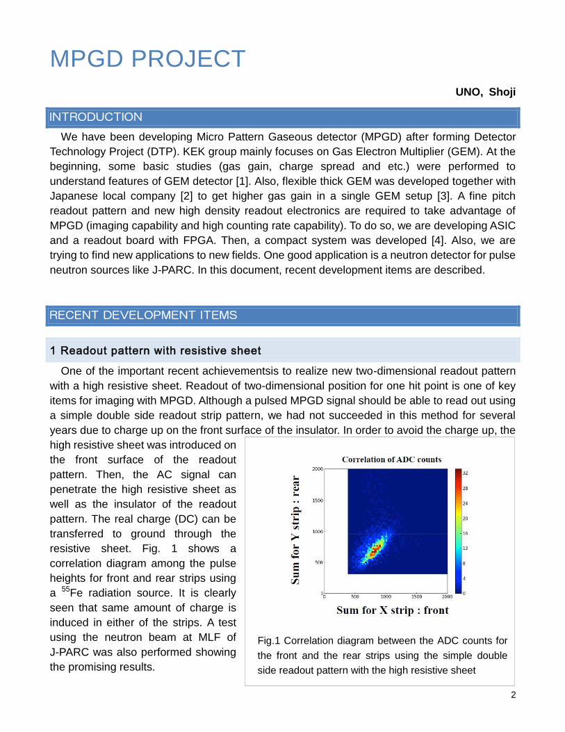
MPGD PROJECT
UNO, Shoji
INTRODUCTION
We have been developing Micro Pattern Gaseous detector (MPGD) after forming Detector
Technology Project (DTP). KEK group mainly focuses on Gas Electron Multiplier (GEM). At the
beginning, some basic studies (gas gain, charge spread and etc.) were performed to
understand features of GEM detector [1]. Also, flexible thick GEM was developed together with
Japanese local company [2] to get higher gas gain in a single GEM setup [3]. A fine pitch
readout pattern and new high density readout electronics are required to take advantage of
MPGD (imaging capability and high counting rate capability). To do so, we are developing ASIC
and a readout board with FPGA. Then, a compact system was developed [4]. Also, we are
trying to find new applications to new fields. One good application is a neutron detector for pulse
neutron sources like J-PARC. In this document, recent development items are described.
RECENT DEVELOPMENT ITEMS
1 Readout pattern with resistive sheet
One of the important recent achievementsis to realize new two-dimensional readout pattern
with a high resistive sheet. Readout of two-dimensional position for one hit point is one of key
items for imaging with MPGD. Although a pulsed MPGD signal should be able to read out using
a simple double side readout strip pattern, we had not succeeded in this method for several
years due to charge up on the front surface of the insulator. In order to avoid the charge up, the
high resistive sheet was introduced on
the front surface of the readout
pattern. Then, the AC signal can
penetrate the high resistive sheet as
well as the insulator of the readout
pattern. The real charge (DC) can be
transferred to ground through the
resistive sheet. Fig. 1 shows a
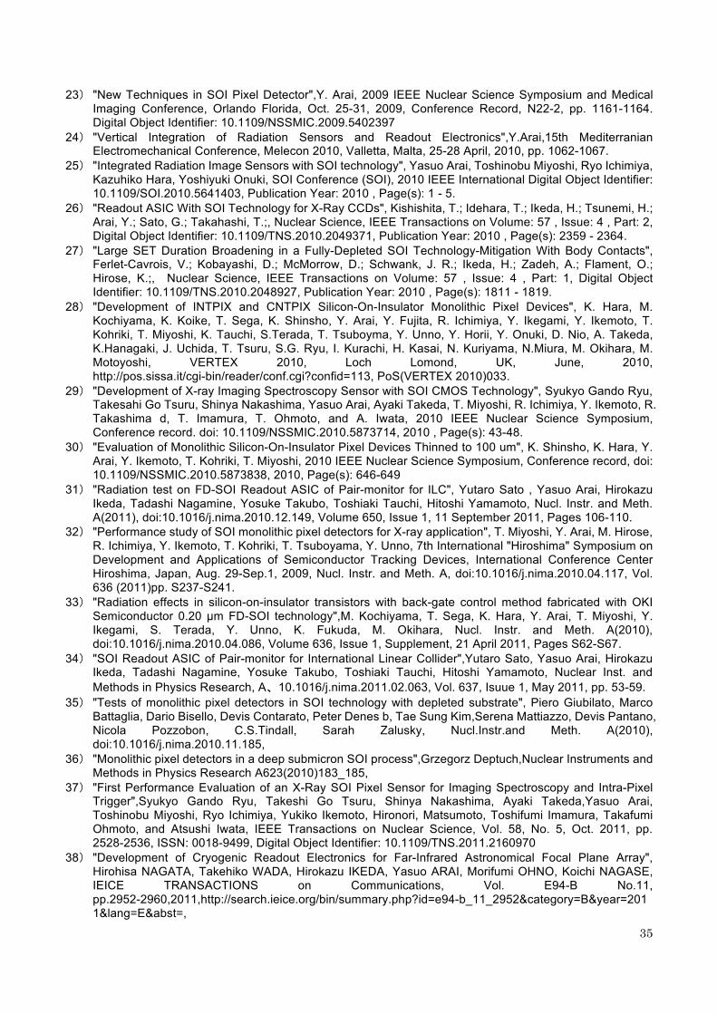
correlation diagram among the pulse
heights for front and rear strips using
a 55Fe radiation source. It is clearly
seen that same amount of charge is
induced in either of the strips. A test
using the neutron beam at MLF of
J-PARC was also performed showing
the promising results.
Fig.1 Correlation diagram between the ADC counts for
the front and the rear strips using the simple double
side readout pattern with the high resistive sheet

3
2 New GEM foils
One serious problem for using GEM detectors is unrecoverable damage caused by a big
discharge. When the damage happens once, the GEM foil should be replaced for operation of
the chamber again. To avoid this problem, the gas gain should be reduced. Also, several new
GEM foils has been developed. One of such GEM foils has resistive electrodes. Even if a small
discharge occurs in one GEM hole, the discharge does not increase. Since large stored charge
does not gather into the hole due to resistivity of electrode. We are developing such GEM foils
and can observe the signal with 55Fe. But, it is not so easy to get the suitable high resistivity
together with suitable etching capability. Other new GEM is to use Teflon instead of Polyamide
(PI) or Liquid Crystal Polymer (LCP) as an insulator. The original problem is carbonization on
the surface of the insulator caused by the big discharge. Teflon has good capability against the
carbonization. It means that the serious damage does not realize even for the big discharge.
We are developing such GEM foils and can see the signal with 55Fe. So far, frequent discharges
occur as compared with normal GEM foils. But, there is no serious damage as expected.
Developing status will be presented in coming review meeting.
3 Electronics
The readout electronics is one of key issues of MPGD development. Recently, we developed
two types of readout boards using ASIC and FPGA. One is higher density and higher readout
event rate capability. Another one is to read out more precise data with moderate readout rate.
3-1 256 channels board
Fig. 2 shows a photo of 256 channels readout board. This board is developed to aim higher
density and higher events rate. One ASIC chip contains 32 channels for preamplifier, shaper
and discriminator. Then, the digital
output signals send to FPGA. The
100 MHz sampling, coincidence
logic for X-Y strips, data formatting
and data transfer function (TCP/IP)
thorough Ethernet are implemented
in FPGA. Fig. 3 shows data transfer
rate with a test pulse. Maximum
speed (12MHz) is limited by 1 Gbps
Ethernet speed. One board (256
channels) matches to 128 channels
for each X and Y strip, which
correspond to 0.8 mm pitch strips in
100×100 mm2 active area. We are
Fig. 2 Photo for 256 channels board. There are 8 ASICs
and one FPGA.

4
using this readout board with the GEM chamber for various applications, which are described
later. Unfortunately, there are some malfunctions in ASIC and the whole 256 channels are not
active. New ASIC chips are under construction and will be available, soon.
3-2 64 channels board
Fig. 4 shows a photo of 64 channels readout board, which is developed very recently. The previous
256 channels readout board can treat digital signals only to get higher event rate. In some cases,
precise measurements for timing and pulse height are required. Therefore, we developed different
readout board, which is
originally developed for
Belle-II CDC readout
system. The precise (1
nsec timing resolution) TDC
is implemented in FPGA
and 30MHz 10 bit FADCs
are mounted on the board
to measure the pulse height
precisely with moderate
channel density (64
channels) and less event
rate (~40 kHz). The data
with this 64 channels board
will be presented in the
coming review meeting.
Fig.3 Event rate using test pulses with the 256 channels board
Fig4. Photo for 64 channels board. There are 6 ASICs, 6 FADCs and one
FPGA.
5
APPLICATIONS
1 Neutron detector
We are trying to apply GEM detectors to various fields. One promising application is a
neutron detector for the pulse neutron sources like J-PARC. In this case, two dimensional
position and timing information are important to measure incident position and wave length of
each neutron, respectively. In order to detect thermal and cold neutrons, boron solid convertor
is used instead of expensive helium-3 gas. In this case, the range for emitted charged particles
(alpha and lithium nucleus) inside the boron convertor is rather short. Therefore, some ideas
are necessary to improve detection efficiency. One idea is to coat thin boron layer on the both
surfaces of GEM foil and stack several foils in one chamber [5]. Another one is to stack boron
coated plates with many holes. In this case, each hole of several plates should be aligned for
ionizing electrons to pass through holes and to reach to the final GEM foil for the amplification.
Detail structures will be presented in the review meeting.
Anyway, one simple application to this kind of neutron detectors is a neutron beam monitor,
since high efficiency is not required. Real monitor system has being used for the beam lines of
MLF in J-PARC to calibrate beam intensity each wave length during whole experimental period
[6,7]. Other interesting application is a detector for an energy selective neutron radiography,
which are described in following sections.
1-1Resonance absorption
Almost all elements have the resonance cross section for neutrons. Usually in the case of
heavy materials resonance cross sections begin to appear at low energy region around eV or
less, and in the case of light materials at higher energy region. So far, relatively low energy
resonances have been used since it is easier to measure than the high energy ones. However,
it is useful to measure the high energy resonances to expand the applicability of the resonance
transmission method. For this, a low noise and high time resolution measurement is required.
Iron is one of the most important materials
and a big resonance exists at 27.7 keV. We try
to measure this resonance by using a GEM
-ray background is very low [8].
Fig. 5 is an example of the transmission
spectrum of a SUS sample. Resonance dips
were observed corresponding to Fe, Mn and
Co. Content of iron is about 70%, Mn 2%, and
Co is impurity in original Ni; so the content is
extremely low. Fig.6 shows a photo of a
SUS304 washer sample and the distribution
of each material by using peaks of iron 27.7
Fig.5An example of transmission spectra
6
keV, Mn 336 eV and Co 135 eV. Here, we succeeded to measure a peak around 30 keV and
also the very low content Co. More results are described in reference [9].
1-2Brag edge analysis
Neutron transmission imaging, namely neutron radiography, is one of useful methods to see
inside of objects. The neutron can easily transmit through major metals and see materials
behind or in the metals although the x-ray cannot. Furthermore, energy selective imaging using
a narrower energy band give a much different image from the traditional wide energy band
images. By using a pulsed neutron source, different contrast images reflecting the cross section
structure were obtained by one measurement. Furthermore, an idea to identify materials in an
object was demonstrated at a pulsed neutron source by analyzing the Bragg edge of the each
material. A map of strain was obtained by analyzing the wavelength of Bragg edge. More detail
analysis method and results are described in references [10,11].
2 Gamma detector
The conventional gamma cameras using NaI(Tl)/PMT scintillation detector have inherent
limitations in spatial resolution, sensitivity, and detector system is very expensive. Gamma
cameras using GEM have been shown to offer potential improvements in basic performance as
compared with conventional gamma cameras at spatial resolution and system costs. In our
camera, a solid converter (gold) is used for the detection of gamma-ray [12]. We have
constructed a small field of view prototype gamma camera with 100mm 100mm GEM foils.
Our system consists of the gamma conversion layers and the amplification layers. The GEM
foils of conversion layer are coated by gold with 3μm thickness on the both surfaces. In order to
obtain higher detection efficiency, several gold-coated GEM foils are stacked. Gold-coated
GEM foils were manufactured and a simple test was carried out to confirm the principle. In order
to know the performance of the prototype gamma camera, gamma-ray irradiation test was
Fig.6 Photo of a washer sample and elemental distributions
7
performed with radioactive source of 99mTc (141keV). Two dimensional images were obtained
using a pinhole collimator as shown in Fig.7. This system enables use of gamma-ray imaging
system in various fields where it has not previously been possible to use such systems. More
information is available in a reference [13]. Recently, this work is not so active due to man
power problem in our group, unfortunately.
Wide spread activities
There are various activities for MPGD development at several universities in Japan. Those
are basically independent. But, closer communication is important to activate various works. To
do so, we had formed a basic study group to exchange information about basic R&D and also
have organized domestic MPGD workshop in Japan once a year at various universities.
Around 80 people including company persons have joined the workshop and have discusses
various items.
Fig.7 (a) Imaging result of a 99m
Tc-filled original resolution phantom constructed from an
acrylic disk in which holes of different sizes (0.5, 1.0, 1.5, 2.0, 2.5 and 3.0 mm) were drilled.
(b,c) Holes are clearly visible down to size of 2.5 mm, which sharp signals in the profile line.
8
SUMMARY
We have been developing new GEM foils and new detectors with new electronics. Some
detectors are already applied for various fields. New GEM foils are promising against the
discharge. New good detectors with high performance will become ready soon.
REFERENCE
[1] S.Uno, et al., 2006 IEEE Nuclear Science Symposium Conference Record N16-4,
“Study of a Charge Distribution on a Readout Board with Triple GEM Chamber”
[2] Scienergy Co. Ltd. ([email protected]). (http://www.scienergy.jp).
[3] S. Uno, et al., Nuclear Instruments and Methods in Physics Research A 581 (2007) 271-273
“Performance study of new thicker GEM”
[4] Tomohisa Uchida, et al., IEEE Trans. Nucl. Sci., vol. 55 No.5 (2008) 2698-2703,
“Prototype of a Compact Imaging System for GEM Detectors”
[5]S. Uno, et al., Physics Procedia 26 (2012) 142-152,
“Two-dimensional Neutron Detector with GEM and its Applications”
[6] H. Ohshita, et al., Nuclear Instruments and Methods in Physics Research A 623 (201)
126-128,
“Development of a neutron detector with a GEM”.
[7] Hidetoshi Ohshita, et al., Nuclear Instruments and Methods in Physics Research A 672
(2012) 75-81,
“Stability of neutron beam monitor for High Intensity Total Diffractometer at J-PARC”.
[8] S.Uno, et al., Physics Procedia 37 (2012) 600-605,
“Development of a two-dimensional gaseous detector for energy-selective neutron
radiography”.
[9] Tesuya Kai, et al., Physics Procedia 43 (2013) 111-120,
“Visibility estimation for neutron resonance absorption radiography using a pulsed neutron
source”.
[10] H. Sato, et al., Materials Transactions, Vol.52 No.06 (2011) 1294-1302,
“A Rietveld-Type Analysis Code for a Pulsed Neutron Bragg-Edge Transmission Imaging and
Quantitative Evaluation of Texture and Microstructure of a Welded Iron”.
[11] K. Kino, et al., Physics Procedia 43 (2013) 360-364,
“Analysis of crystallographic structure of a Japanese sword by the pulsed neutron transmission
method”.
[12] Takahisa Koike, et al., Nuclear Instruments and Methods in Physics Research A 648 (2011)
180-185,
“A new gamma-ray detector with gold-plated gas electron multiplier”.
[13] T. Koike, et al., 2012 JINST 7 C01078,
“A new gamma camera with a Gas Electron Multiplier”.

9
SCD PROJECT (SUPERCONDUCTING DETECTOR)
HAZUMI, Masashi
INTRODUCTION
Superconducting Detectors (SCDs) are the detectors consisting of superconducting materials.
In the superconductors, Cooper pairs play an essential role in the detection principle; because
of the small binding energy of Cooper pairs, an order of milli-electron volt, SCD in general has
very high sensitivity to the electromagnetic waves whose wavelength ranges from millimeter to
gamma rays. The SCD can be applied to a wide range of fields: particle physics, astronomy,
material science, and so on.
There are several kinds of SCDs. Examples are TES (transition edge sensor) bolometer,
MMC (metallic magnetic calorimeter), STJ (Superconducting Tunnel Junction) and KID (Kinetic
Inductance Detector). The SCD group in the KEK Detector Technology Project has been
developing mainly STJ and KID. We report on the development status of the SCD in our group.
The SCDs are fabricated using a facility in KEK with a lithography technique. The facility has
been operating from 2009, and contains two sputter machines to form thin layers of metal and
insulator, two etching machines, a yellow room for the development and the patterning, an
optical microscope, a profile meter, a SEM and an AMF. We use a helium-3 sorption refrigerator
able to cool the detectors down to 0.3K for the detector evaluation.
STJ (SUPERCONDUCTING TUNNEL JUNCTION)
The STJ has the Josephson junction of sandwich-like SIS (superconductor insulator
superconductor) structure. The insulator layer is formed with oxide aluminum and has a
thickness of about 1nm. For the superconductors, we use Hf, Al or a combination of Al and Nb.
The Cooper pair binding energy ( ), which equals to the gap energy in the superconductor, is
given as , where is the Boltzmann constant and is the critical
temperature at which the normal metal transforms to the superconductor. For example, the
binding energy is 0.34 meV = 82 GHz for Al which has K.
Figure 1: Detection principles of the STJ

10
The detection principles of the STJ are shown in Fig. 1. The direct Cooper pair breaking can
be caused by a photon or a phonon with the energy greater than the binding energy ,
generating quasi-particles. The quasi-particles can penetrate the insulator layer by tunneling.
The second principle is called the photon associated tunneling. An electron in the valence band
can jump to the conducting band through tunneling by the assist of a photon and the bias
voltage applied to the SIS junction. In this case, the photon with energy greater than
can be detected, where is the bias voltage. Therefore the STJ can in principle directly detect
photons with energies less than . This is one of the advantages of the STJ since the STJ can
detect millimeter wave photons with frequencies less than 82 GHz by using Al, while the KID
cannot. Other advantages of the STJ include the large dynamic range of 106, the fast response
of order of micro-seconds, and no need of the fine temperature control below 0.6 K for Nb/Al
STJs compared with the TES bolometers.
We have been developing STJs for detections of millimeter waves and infrared photons. The
former is for cosmic microwave background detection and the latter is for the detection of
photons from the decays of cosmic neutrinos.
2-1 The STJ for millimeter waves
At the first stage, we developed PCTJ (parallel connected twin junction) detector. The twin
parallel STJs and the inductance induced by the microstrip line between the STJs form a
resonant circuit. The circuit can accumulate the millimeter wave energy that breaks Cooper
pairs. We successfully took a picture as shown in Fig. 2 with 90GHz millimeter waves. We,
however, found that the control to tune the resonant frequencies is not easy due to the
fabrication.
Instead we have designed a microstrip transmission type STJs shown in Fig. 3. The
log-periodic antenna has a capability to receive a broad bandwidth with the impedance
independent of frequencies. The lower frequency limit is determined by the size of the antenna.
Figure 2: (Left) Metal mask on the polyethylene substrate. (Right) Picture taken by a
single antenna-coupled PCTJ detector using the mask with 90GHz millimeter waves.
The mask was moved by 1mm step in the xy plane.
11
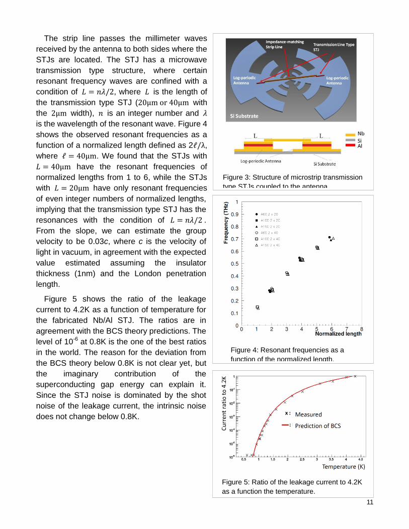
The strip line passes the millimeter waves
received by the antenna to both sides where the
STJs are located. The STJ has a microwave
transmission type structure, where certain
resonant frequency waves are confined with a
condition of , where is the length of
the transmission type STJ ( with
the width), is an integer number and
is the wavelength of the resonant wave. Figure 4
shows the observed resonant frequencies as a
function of a normalized length defined as 2 ,
where . We found that the STJs with
have the resonant frequencies of
normalized lengths from 1 to 6, while the STJs
with have only resonant frequencies
of even integer numbers of normalized lengths,
implying that the transmission type STJ has the
resonances with the condition of .
From the slope, we can estimate the group
velocity to be 0.03c, where c is the velocity of
light in vacuum, in agreement with the expected
value estimated assuming the insulator
thickness (1nm) and the London penetration
length.
Figure 5 shows the ratio of the leakage
current to 4.2K as a function of temperature for
the fabricated Nb/Al STJ. The ratios are in
agreement with the BCS theory predictions. The
level of 10-6 at 0.8K is the one of the best ratios
in the world. The reason for the deviation from
the BCS theory below 0.8K is not clear yet, but
the imaginary contribution of the
superconducting gap energy can explain it.
Since the STJ noise is dominated by the shot
noise of the leakage current, the intrinsic noise
does not change below 0.8K.
Figure 3: Structure of microstrip transmission
type STJs coupled to the antenna.
Figure 4: Resonant frequencies as a
function of the normalized length.
Figure 5: Ratio of the leakage current to 4.2K
as a function the temperature.
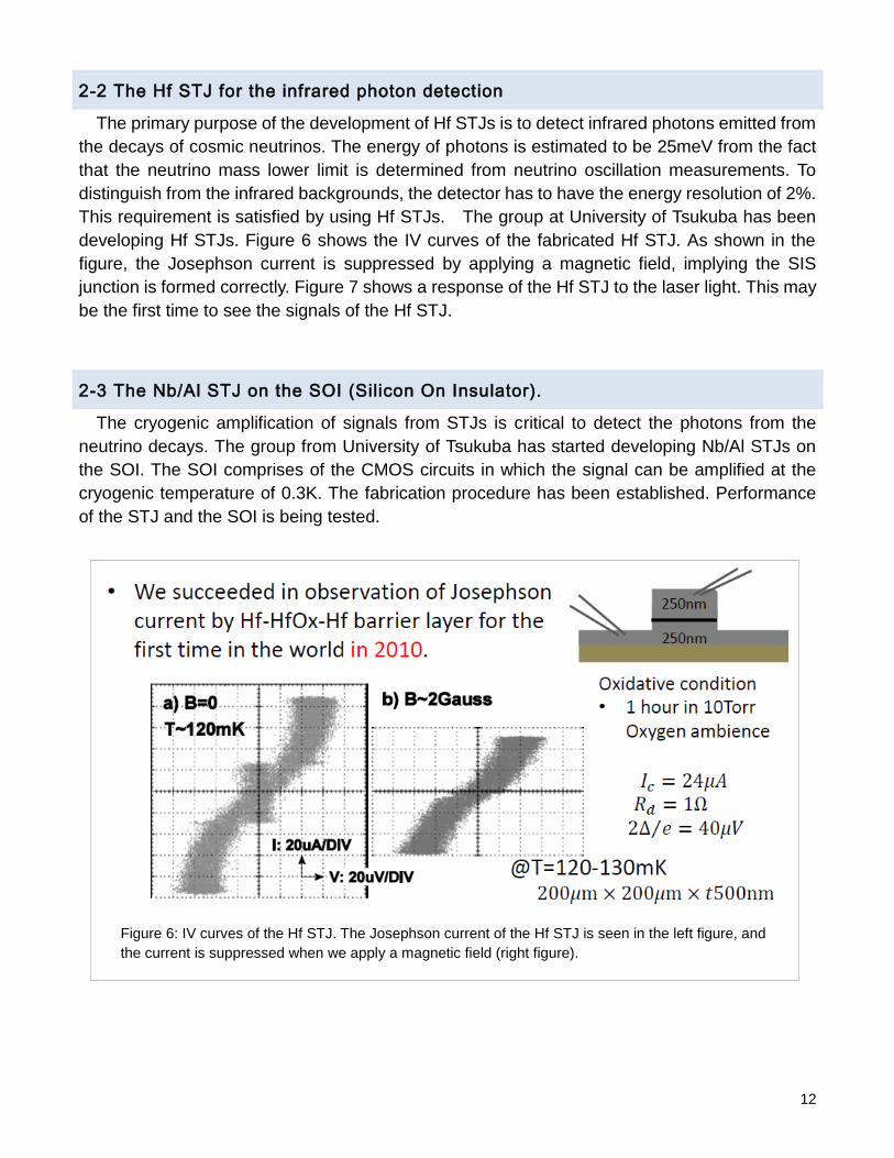
12
2-2 The Hf STJ for the infrared photon detection
The primary purpose of the development of Hf STJs is to detect infrared photons emitted from
the decays of cosmic neutrinos. The energy of photons is estimated to be 25meV from the fact
that the neutrino mass lower limit is determined from neutrino oscillation measurements. To
distinguish from the infrared backgrounds, the detector has to have the energy resolution of 2%.
This requirement is satisfied by using Hf STJs. The group at University of Tsukuba has been
developing Hf STJs. Figure 6 shows the IV curves of the fabricated Hf STJ. As shown in the
figure, the Josephson current is suppressed by applying a magnetic field, implying the SIS
junction is formed correctly. Figure 7 shows a response of the Hf STJ to the laser light. This may
be the first time to see the signals of the Hf STJ.
2-3 The Nb/Al STJ on the SOI (Silicon On Insulator).
The cryogenic amplification of signals from STJs is critical to detect the photons from the
neutrino decays. The group from University of Tsukuba has started developing Nb/Al STJs on
the SOI. The SOI comprises of the CMOS circuits in which the signal can be amplified at the
cryogenic temperature of 0.3K. The fabrication procedure has been established. Performance
of the STJ and the SOI is being tested.
Figure 6: IV curves of the Hf STJ. The Josephson current of the Hf STJ is seen in the left figure, and
the current is suppressed when we apply a magnetic field (right figure).

13
KID (KINETIC INDUCTANCE DETECTOR)
Superconductors in general have the kinetic inductance that arises from the total kinetic
energy of Cooper pairs. When energy is deposited to the superconductor and some Cooper
pairs are broken, the net kinetic energy, hence the kinetic inductance, is changed. If we form a
resonator with the superconductor, the Cooper pair breaking causes the change of the resonant
frequency. KIDs make use of this mechanism to detect the deposit energy of photons or
phonons. The features of the KID are: (1) frequency domain multiplexing, enabling us to
readout hundreds of resonators with a single cable, (2) a simple structure consisting of a single
or double metal layer(s) and (3) needlessness of the bias.
We have been developing KIDs for detections of phonons, optical photons and millimeter
waves. The phonon detection aims to detect dark matter and X-rays in the substrate. The
optical photon detection may be applied to a liquid-helium TPC to detect UV scintillation
photons. The millimeter wave detection is for the CMB polarization measurements.
Figure 7: Laser pulse response of the Hf STJ. Top line shows the output current of the Hf STJ.
Middle is laser pulse trigger timing.
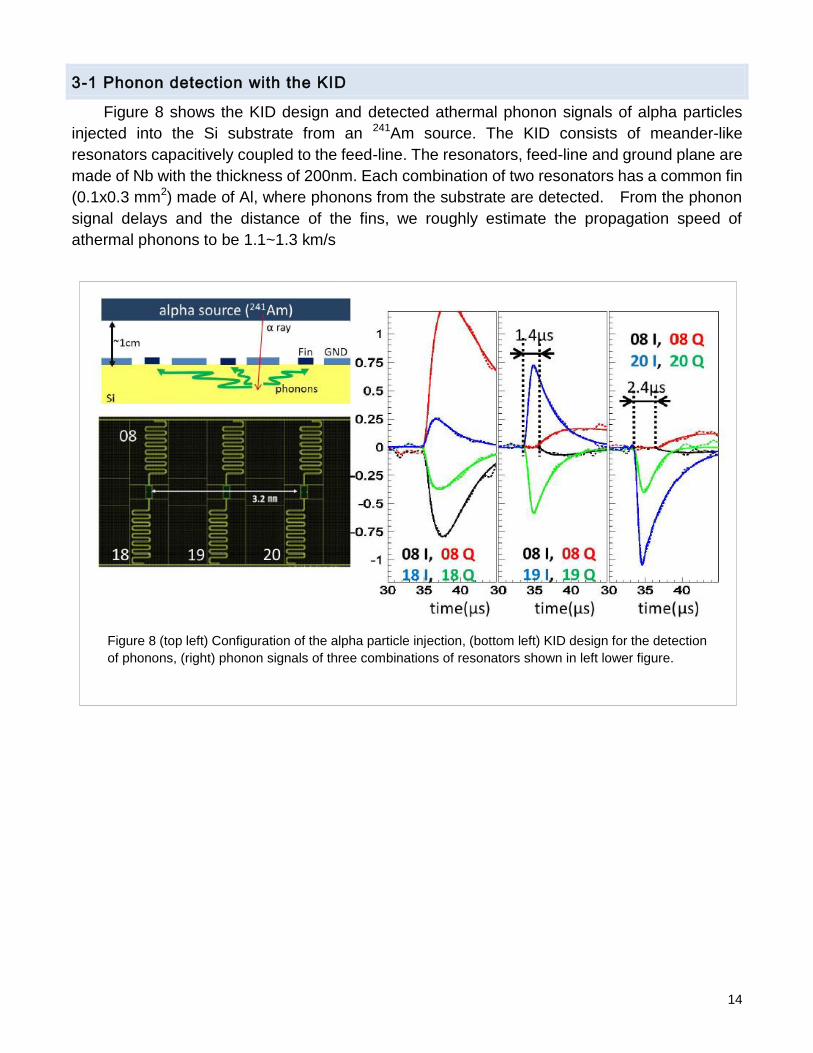
14
3-1 Phonon detection with the KID
Figure 8 shows the KID design and detected athermal phonon signals of alpha particles
injected into the Si substrate from an 241Am source. The KID consists of meander-like
resonators capacitively coupled to the feed-line. The resonators, feed-line and ground plane are
made of Nb with the thickness of 200nm. Each combination of two resonators has a common fin
(0.1x0.3 mm2) made of Al, where phonons from the substrate are detected. From the phonon
signal delays and the distance of the fins, we roughly estimate the propagation speed of
athermal phonons to be 1.1~1.3 km/s
Figure 8 (top left) Configuration of the alpha particle injection, (bottom left) KID design for the detection
of phonons, (right) phonon signals of three combinations of resonators shown in left lower figure.
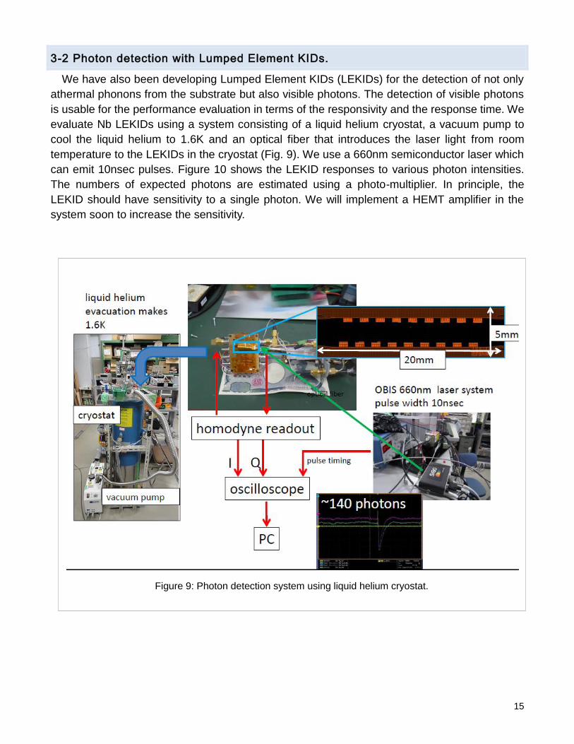
15
3-2 Photon detection with Lumped Element KIDs.
We have also been developing Lumped Element KIDs (LEKIDs) for the detection of not only
athermal phonons from the substrate but also visible photons. The detection of visible photons
is usable for the performance evaluation in terms of the responsivity and the response time. We
evaluate Nb LEKIDs using a system consisting of a liquid helium cryostat, a vacuum pump to
cool the liquid helium to 1.6K and an optical fiber that introduces the laser light from room
temperature to the LEKIDs in the cryostat (Fig. 9). We use a 660nm semiconductor laser which
can emit 10nsec pulses. Figure 10 shows the LEKID responses to various photon intensities.
The numbers of expected photons are estimated using a photo-multiplier. In principle, the
LEKID should have sensitivity to a single photon. We will implement a HEMT amplifier in the
system soon to increase the sensitivity.
Figure 9: Photon detection system using liquid helium cryostat.
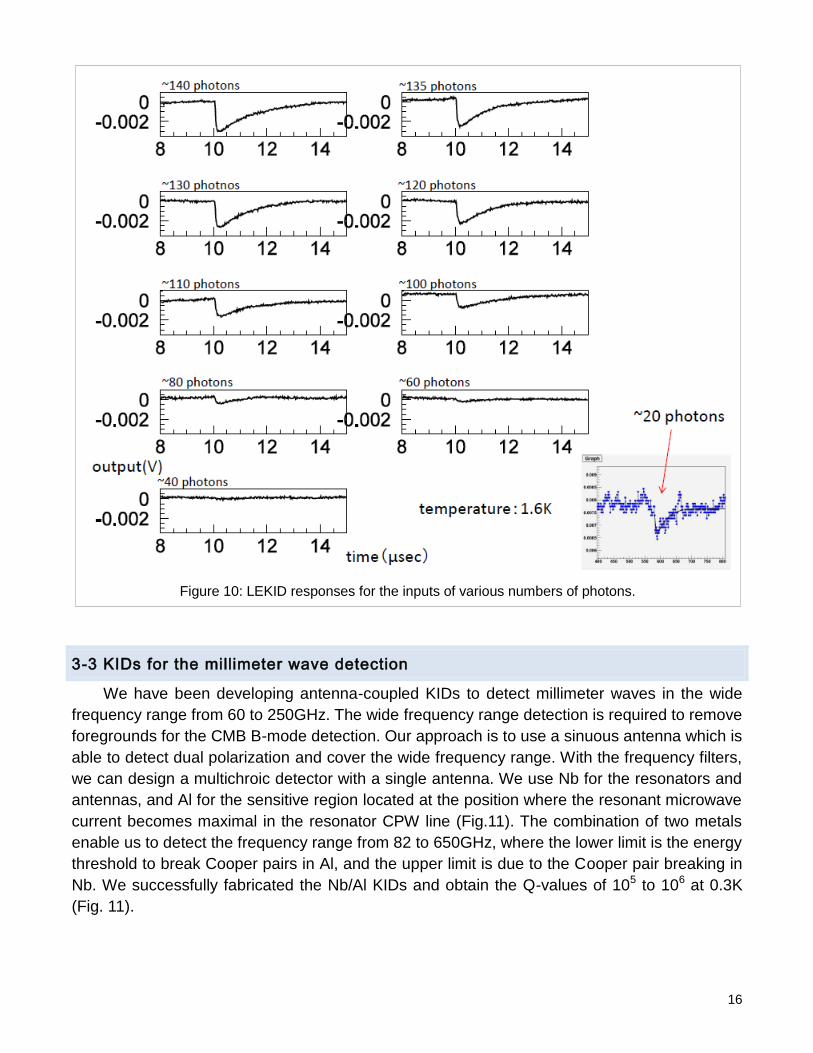
16
3-3 KIDs for the millimeter wave detection
We have been developing antenna-coupled KIDs to detect millimeter waves in the wide
frequency range from 60 to 250GHz. The wide frequency range detection is required to remove
foregrounds for the CMB B-mode detection. Our approach is to use a sinuous antenna which is
able to detect dual polarization and cover the wide frequency range. With the frequency filters,
we can design a multichroic detector with a single antenna. We use Nb for the resonators and
antennas, and Al for the sensitive region located at the position where the resonant microwave
current becomes maximal in the resonator CPW line (Fig.11). The combination of two metals
enable us to detect the frequency range from 82 to 650GHz, where the lower limit is the energy
threshold to break Cooper pairs in Al, and the upper limit is due to the Cooper pair breaking in
Nb. We successfully fabricated the Nb/Al KIDs and obtain the Q-values of 105 to 106 at 0.3K
(Fig. 11).
Figure 10: LEKID responses for the inputs of various numbers of photons.

17
3-4 A KID readout system
The multiplexing readout system is being developed using a Kintex-7 FPGA board DSP kit
available commercially. With the help from Open-It, we have been developing firmware codes
that generate a frequency comb for the KID resonator excitation and generate I/Q signals for
each resonator (Fig. 12). We have confirmed a successful performance of simultaneous
readout with 32 channels at a sampling rate of 1kHz. Because of the capacity of the
look-up-table in the FPGA chip and the digital signal timing limitation, we expect the 100
channel readout at maximal.
Figure 11 (left) KID design showing the sinuous antennas coupled to the resonators,
(right)Q-values as a function of the temperature.
Figure 12: (Left) Kintex-7 FPGA board we are using. (Right) Block Diagram of the
generation of a frequency comb and I/Q signals with the homodyne readout.
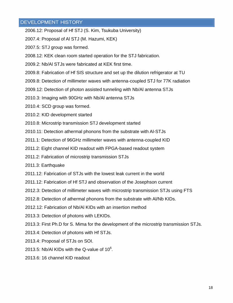
18
DEVELOPMENT HISTORY
2006.12: Proposal of Hf STJ (S. Kim, Tsukuba University)
2007.4: Proposal of Al STJ (M. Hazumi, KEK)
2007.5: STJ group was formed.
2008.12: KEK clean room started operation for the STJ fabrication.
2009.2: Nb/Al STJs were fabricated at KEK first time.
2009.8: Fabrication of Hf SIS structure and set up the dilution refrigerator at TU
2009.8: Detection of millimeter waves with antenna-coupled STJ for 77K radiation
2009.12: Detection of photon assisted tunneling with Nb/Al antenna STJs
2010.3: Imaging with 90GHz with Nb/Al antenna STJs
2010.4: SCD group was formed.
2010.2: KID development started
2010.8: Microstrip transmission STJ development started
2010.11: Detection athermal phonons from the substrate with Al-STJs
2011.1: Detection of 96GHz millimeter waves with antenna-coupled KID
2011.2: Eight channel KID readout with FPGA-based readout system
2011.2: Fabrication of microstrip transmission STJs
2011.3: Earthquake
2011.12: Fabrication of STJs with the lowest leak current in the world
2011.12: Fabrication of Hf STJ and observation of the Josephson current
2012.3: Detection of millimeter waves with microstrip transmission STJs using FTS
2012.8: Detection of athermal phonons from the substrate with Al/Nb KIDs.
2012.12: Fabrication of Nb/Al KIDs with an insertion method
2013.3: Detection of photons with LEKIDs.
2013.3: First Ph.D for S. Mima for the development of the microstrip transmission STJs.
2013.4: Detection of photons with Hf STJs.
2013.4: Proposal of STJs on SOI.
2013.5: Nb/Al KIDs with the Q-value of 106.
2013.6: 16 channel KID readout
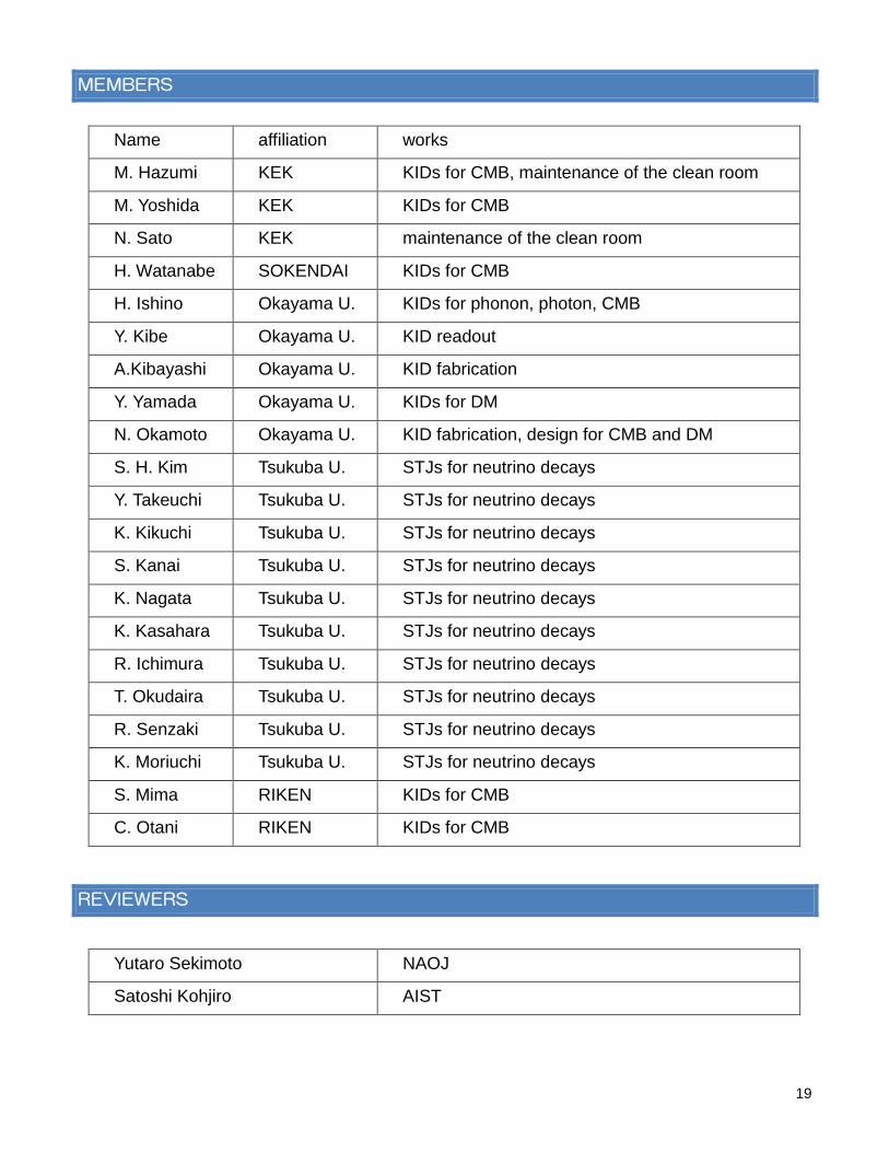
19
MEMBERS
Name affiliation works
M. Hazumi KEK KIDs for CMB, maintenance of the clean room
M. Yoshida KEK KIDs for CMB
N. Sato KEK maintenance of the clean room
H. Watanabe SOKENDAI KIDs for CMB
H. Ishino Okayama U. KIDs for phonon, photon, CMB
Y. Kibe Okayama U. KID readout
A.Kibayashi Okayama U. KID fabrication
Y. Yamada Okayama U. KIDs for DM
N. Okamoto Okayama U. KID fabrication, design for CMB and DM
S. H. Kim Tsukuba U. STJs for neutrino decays
Y. Takeuchi Tsukuba U. STJs for neutrino decays
K. Kikuchi Tsukuba U. STJs for neutrino decays
S. Kanai Tsukuba U. STJs for neutrino decays
K. Nagata Tsukuba U. STJs for neutrino decays
K. Kasahara Tsukuba U. STJs for neutrino decays
R. Ichimura Tsukuba U. STJs for neutrino decays
T. Okudaira Tsukuba U. STJs for neutrino decays
R. Senzaki Tsukuba U. STJs for neutrino decays
K. Moriuchi Tsukuba U. STJs for neutrino decays
S. Mima RIKEN KIDs for CMB
C. Otani RIKEN KIDs for CMB
REVIEWERS
Yutaro Sekimoto NAOJ
Satoshi Kohjiro AIST

20
DISSERTATIONS
PhD:
Satoru Mima, Okayama University, Mar. 2013, ``Development of Microstrip Transmission
Type STJs for the millimeter/sub-millimeter astronomy.''
Master of science:
Kazuki Nagata, University of Tsukuba, Feb. 2013, ``Development of Hf STJs for detections of
photons from the neutrino decays.''
Shinya Kanai, University of Tsukuba, Feb. 2013, ``Development of Nb STJs for the detections
of infrared photons.''
Taiki Yuasa, Okayama University, Feb. 2013, ``Development of Microwave Kinetic
Inductance Detectors with the combination of Nb and Al.''
Kenji Kiuchi, University of Tsukuba, Feb. 2011, ``Development of Hf STJs having the high
energy resolution.''
Noriko Ogura, Okayama University, Feb. 2011, ``Design of Microwave Kinetic Inductance
Detectors using a simulation.''
H. Jing, University of Tsukuba, Feb. 2010, ``Development of Hf STJs for far-infrared
photons.''
Ken-ichi Takemasa, University of Tsukuba, Feb. 2009, ``Development of Hf STJs for the
detection of photons from neutrino decays.''
PUBLICATIONS
[1]``MKID and its application to cosmology and particle physics'', H. Ishino, M. Hazumi, A.
Kibayashi, Y. Kibe, S. Mima, N. Sato, M. Yoshida and H. Watanabe, IEICE Technical Report
SCE2012-22, 17 (2013).
[2]``Development of Microwave Kinetic Inductance Detectors and their Readout System for
LiteBIRD'', K. Hattori et al., in press in NIMA.
21
[3]``Development of Superconducting Detectors'', H. Ishino, M. Hazumi, S. Mima and M.
Yoshida, High energy news, Vol. 32, Number 1, pp.24-33 (2013).
[4]``Development of Superconducting Detectors for Measurements of Cosmic Microwave
Background, K. Hattori et al., Phys. Proc. 37, pp.1406 - 1412 (2012).
[5]``Novel Frequency-Domain Multiplexing MKID Readout for the LiteBIRD Satellite'', J. of
Low Temp. Phys., 167, Issue 5, pp.671 - 677 (2012).
[6]``Development of Superconducting Tunnel Junction Photon Detector using Hafnium'',
S.H. Kim, H.S. Jeong, K. Kiuchi, S. Kanai, T. Onjo, K. Takemasa, Y. Takeuchi, H. Ikeda, S.
Matsuura, H. Sato, M. Hazumi and S.B. Kim., Phys. Proc. 37, pp.667-674 (2012).
PRESENTATIONS
``MKID and its application to cosmology and particle physics'', H. Ishino, Workshop for the
superconducting electronics, Tohoku University, Sendai, Japan, Oct. 2nd, 2013.
“Search for Cosmic Background Neutrino Decay with STJ detectors” Y. Takeuchi, MKID
and Cosmology Workshop @FNAL, Aug. 26-27, 2013,
"Search for Cosmic Background Neutrino Decay" S. H. Kim, APPC12 @ Makuhari, July 17,
2013
“Development of the Superconducting Detectors for Applications to Particle Physics and
Astrophysics” (poster), A. Kibayashi, APPC12, Makuhari, Japan, July14-19, 2013
``Development of Microwave Kinetic Inductance Detectors for a detection of phonons'',
(poster) H. Ishino, Low Temperature Detectors 15, Pasadena, USA, Jun. 24th, 2013.
``Low Noise Readout System for MKIDs with Frequency-domain Technique towards
application of CMB observation'', (poster) Y. Kibe, Low Temperature Detectors 15, Pasadena,
USA, Jun. 24th, 2013.

22
``Hybrid MKIDs with ground-side deposition -- A novel method for microwave detection with a
resonator separated from an antenna'', (poster), H. Watanabe, Low Temperature Detectors 15,
Pasadena, USA, Jun. 24th, 2013.
``Transmission line type STJ coupled with a broad band antenna for millimeter and
sub-millimeter wave detections'', (poster), S. Mima, CMB2013, OIST, Okinawa, Jun. 2013.
"Search for Cosmic Background Neutrino Decay" (poster) S. H. Kim, SPICA International
Conference 2013 @ University of Tokyo, June 18-21, 2013
"Search for Cosmic Background Neutrino Decay" (poster) Y. Takeuchi, CMB2013,
International Conference on Cosmic Microwave Background Jun. 10-14, 2013 @ OIST,
Okinawa
"Development of Superconducting Tunnel Junction Photon Detector on SOI Preamplifier
Board to Search for Radiative Decays of Cosmic Background Neutrino“ (poster) K. Kasahara,
CMB2013, International Conference on Cosmic Microwave Background Jun. 10-14, 2013 @
OIST, Okinawa
"Development of Nb/Al superconducting tunnel junction detector of a single infrared photon to
search for radiative decay of the cosmic background neutrinos“ (poster) T.Okudaira, :
CMB2013, International Conference on Cosmic Microwave Background Jun. 10-14, 2013 @
OIST, Okinawa
``Development of Microwave Kinetic Inductance Detectors and its Readout System for
LiteBIRD'', (poster), Y. Kibe, VCI2013, Viena, Austria, Feb, 2013.
``Development of Microwave Kinetic Inductance Detector and its Read-out System for
LiteBIRD'', (poster), Y. Kibe, ISSTT2012, Mitaka, Japan, Apr. 2012.
``Novel Frequency-domain multiplexing MKID readout for the LiteBIRD satellite'', (poster), K.
Hattori, LTD14, Heidelberg, Germany, Aug. 2011.
``Development of Superconducting Detectors for Measurements of Cosmic Microwave
Background'', S. Mima, TIPP2011, Chicago, USA, Jun. 2011.
23
``Developments of Aluminum Superconducting Tunnel Junction (STJ) detectors for millimeter
wave and particle detections'', (poster), H. Ishino, TIPP2011, Chicago, USA, Jun. 2011.
``Development of Microwave Kinetic Inductance Detectors (MKIDs) for Cosmic Microwave
Background Polarization detection with the LiteBIRD Satellite'', H. Watanabe, The 11th
Workshop on Submillimeter-wave Receiver Technologies in Eastern Asia, Nagoya, Japan, Nov.
2010.
``Development of an Antenna-coupled Al Superconducting Tunnel Junction for a detection of
Cosmic Microwave Background B-mode Polarization'', (poster), H. Ishino, TIPP2009, Tsukuba,
Japan, Mar. 2009.
RESEARCH FUNDS
Grant-in-Aid for Scientific Research on Innovative Areas, S.B. Kim, FY 2013-2017.
Grant-in-Aid for Scientific Research on Innovative Areas, M. Hazumi FY 2009-2013.
Grant-in-Aid for Challenging Exploratory Research, H. Ishino, FY 2012-2013
Grant-in-Aid for Challenging Exploratory Research, H. Ishino, FY 2010-2011
Grant-in-Aid for Young Scientists (A), H. Ishino, FY 2010-2012.
KEK research support program, H. Ishino, FY 2010-2012.
KEK research support program, H. Ishino, FY 2008-2009
KEK research support program, S. H. Kim, FY 2008-2013.
WORKSHOPS
``Superconducting Camera and related technology -- Application to the astronomy and
cosmology'', KEK, Feb. 20-21, 2009.
24
LIQUID TPC PROJECT
LIQUID ARGON TPC
MARUYAMA, Takasumi
SUMMARY OF ACTIVITY DURING 2008-2013
DTP has started the R&D activity on LAr TPC since 2008. This activity is the newest projects
in the DTP.
In 2008, 10L prototype vessel is made to test the readout system for TPCs and to obtain the
experience of the cryogenic system, (Fig.1)
This system consists of an inner vessel, a LAr open bath to cool down, commercial H2O and
O2 filters and vacuum pumps. Inside the inner vessel, hand-made TPC was put as shown in
Fig.1. At the beginning of the test, we use 4ch cupper readout system. The electric field shapers
and anode-grid with stainless wires of 100 m diameter, and 5mm pitch, are made from
stainless plates. Total size of the TPC is 10cm x 10cm x 5 cm. The vacuum evacuation inside
the inner vessel (10-4 Pa level) was performed at first, the cooling down with LAr filled in the
Fig.1 10L test system. Top-right shows the schematic view, and top-left shows a picture of the setup.
Bottom pictures show the TPC inside the inner vessel.
25
bath and then gas argon is filled inside the inner vessel. Gas argon is liquefied at the end. In
2009, we successfully saw the cosmic ray using the system. Achieved purity is about a few ppb
(parts-per-billion) using the set-up.
The latter of 2009, we started the R&D for the 250L system. The primary goal of the R&D is to
check the detector response of K particles with the beam (J-PARC T32), especially at low
momentum, which is similar to the decay products of the proton decay range. The cryostat
(Fig.2, left) was borrowed from the MEG collaboration [1] for the test-beam. In October 2010,
we saw the beautiful tracks of kaons, pions, protons, and positrons. (An example of tracks are
shown in right plot in Fig.2 ). During this test-beam for a week, the purity is kept to be around
0.8 ppb with gas recirculation system (it had been slightly degraded during the test-beam).
CAEN high voltage (HV) supplier provides the 9 kV to the cathode plane typically and 12 kV at
maximum. (the drift electric field is 200V/cm typically and 250kV/cm at maximum). There are
possibilities to have sparks in gas argon usually, therefore the gas-tight high voltage
feed-through is important for DC HV system. At anode-grid plane, which is put 1cm below the
anode, 1 kV is supplied for typical case, and 2 kV is supplied at maximum case, respectively.
This readout system is crude and 1D, but some preliminary results of the analysis have been
shown in many DTP reviews and international conferences, especially for the DQ/dx analysis
[2].
From 2011 to 2012, upgrades of the cryo-systems (especially gas recirculation system), HV
and readout systems have been performed.
Fig.3 shows the upgrade of the gas recirculation and the cryo-system.
Fig.2 Left; Schematic view of the 250L system. TPC was made by PC4 circuit board (middle pictures).
Size of the TPC is 40x40x80cm3. The readout plane was 76 ch (1cm/ch) 1D readout, and connected from
TPC to feed-through by twist-flat cables. After the feed-through, electric signal is going to CAEN SY2791
board. Right; one typical tracks (top; pion, middle; positron, bottom; proton)
26
As shown in Fig.3 (green line and dark gray in top-left schematic and bottom middle picture),
a cryo-cooler and LN2 coil is put on the top flange of the 250L in 2010. They degraded purity of
LAr due to condensing the dirty gas argon around the coolers. Thus the new gas argon
condenser is inserted into the gas recirculation system, not attached in top flange of the system
directly. To reduce the heat load in the gas recirculation system, the heat exchanger is also
inserted in the system as shown in top-right schematic and bottom-right picture of Fig.3. Due to
the upgrade of the system, the purity is kept to be about 0.3 ppb for a few months. After the
test-beam in 2010, we return the 250L vessel to the MEG collaboration, and we remade the
replica of the 250L cryostat. The LN2 pipes surround the inner vessel of the cryostat, therefore
the pre-cooling can be done more smoothly.
The hand-made O2 filter has been used for direct LAr purification (blue line in schematics in
Fig.3) since 2010. Bottom-left picture in Fig.3 shows the vessel of the filter. Inside the vessel,
the proper size powders of cupper and molecular sieve are filled in. The careful regeneration
procedure is needed in order to use this filter before the operation.
Cockcloft-Walton (CW) circuit is adapted for the high voltage system after 2010 as shown in
Fig.4. CW uses capacitors and diodes in ladders (top drawings in Fig.4) and the only low AC
voltage is needed in the feed-through part. The possibility of the spark in the gas argon is
Fig3; Left; gas recirculation and cryo system in 2010. Right; those in 2012. Gas recirculation system is
connected to “gas pump” in the figures. Green lines correspond to liquid nitrogen system. Liquid argon is
stored in the blue tanks, and filled into the inner cryostat via O2 filters. Pictures show O2 filter, cryo-cooler
head, heat exchanger and LAr condenser.

27
reduced. We use 40 stages (1cm/1stage in TPC) for CW system, and each CW stage supply
high voltage to field shaper as shown in the bottom picture in Fig.4. The comparison between
the simulation (LTspice) and the measurement was carefully done (bottom-right). A linearity of
the circuit is kept about a few % level at the final stage at the cathode. Note that the simulation
uses the property of the diode made by the company, and it is essential to make the realistic
result of the simulation. This system successfully supplied the high voltage up to 60 kV. One
caveat is that there is large noise during charging the CW system, therefore we turn off the CW
system after the charging, which takes one minute typically. We recharge the system every 12
hours, which cause 5% drop of the cathode voltage.
The readout system is upgraded to 2-dimensional and 4mm pitch using a print circuit board in
2013. Small prototype test was done using 10L system in summer 2012, and a large board was
adapted for the 250L system in 2013. Fig.5 shows the picture and schematic view of the new 2D
readout system. There are number of 1mm x 1mm pads in the plane, and 4 raws and 4 columns
are connected one per each two pads for x and y readout as shown in left schematic view in
Fig.5. This system has an advantage that we can use the same software programs to analyze
both x-z and y-z planes. However, the readout system has half of the charge compared to the
wire readout system since it shares the charge. I.e.; noise level of the detector and readout
system should be minimum to use this kind of system.
Fig.4; A drawing of the CW circuit (top). Bottom-left; picture of CW. Bottom-right; Comparison between simulation (LTspice) and measurements of voltage every five stages.

28
Fig.6 shows a typical cosmic ray event using all upgrades mentioned above. Top plot shows
the x-z view while the bottom plot shows the y-z view. Vertical axis corresponds to drift time
axis, and horizontal axis is the x (top) and y (bottom), respectively. Signal-to-noise ratio should
be improved, but the first cosmic ray event provides the evidence that the scheme works well.
Fig.5; New readout plane. (bottom-right); picture of the readout plane. (top-right); picture of the
boards. Left; schematic which shows the principle of the board.
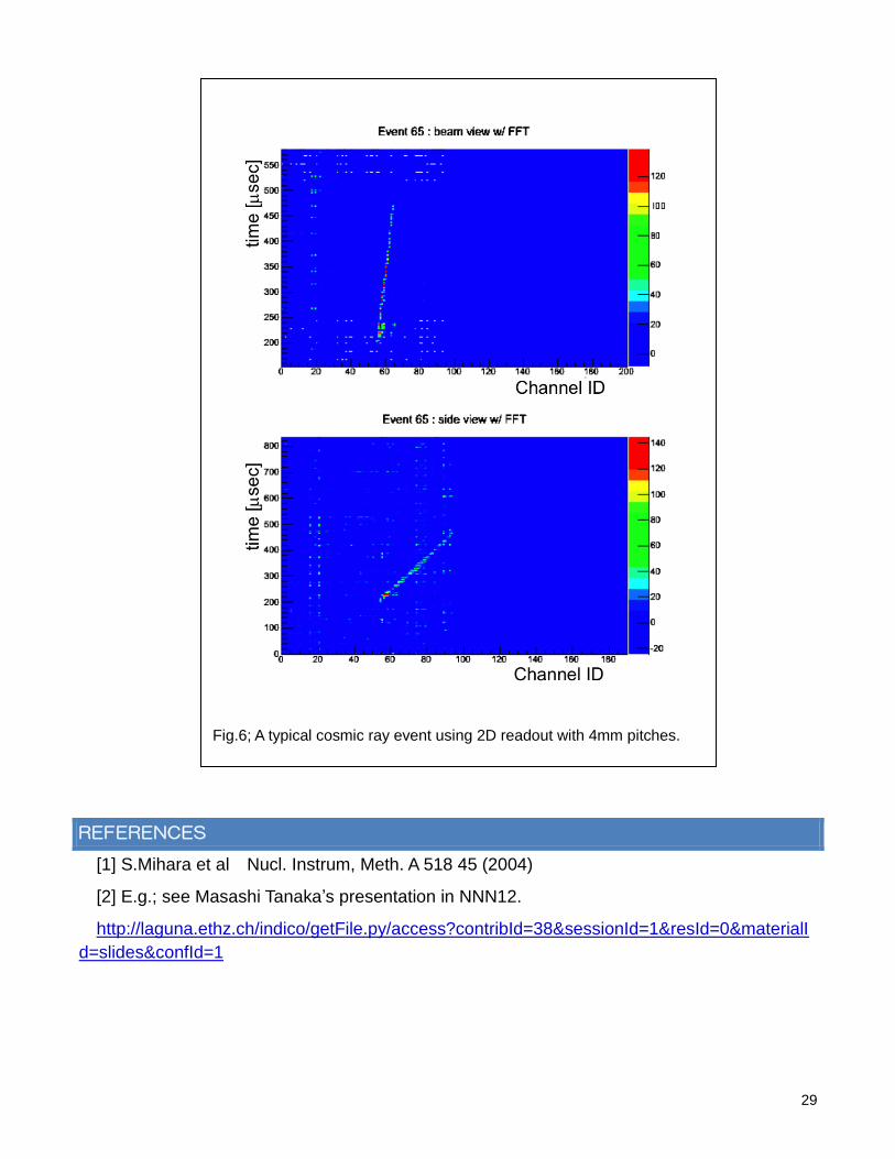
29
REFERENCES
[1] S.Mihara et al Nucl. Instrum, Meth. A 518 45 (2004)
[2] E.g.; see Masashi Tanaka’s presentation in NNN12.
http://laguna.ethz.ch/indico/getFile.py/access?contribId=38&sessionId=1&resId=0&materialI
d=slides&confId=1
Fig.6; A typical cosmic ray event using 2D readout with 4mm pitches.
30
PUBLICATIONS (2010-2013)
O.Araoka, et al “A tagged low-momentum kaon test-beam exposure with a 250L LAr TPC
(J-PARC T32)” J. Phys. Conf. Ser. 308, 012008 (2011)
M.Tanaka, et al “Recent results from Liquid Argon R&D at KEK” J. Phys. Conf. Ser. 308,
012008 (2011)
T.Maruyama “R&D towards huge liquid argon detectors for nucleon decay, neutrino
astrophysics and CP-violation in the lepton sector”, AIP Conf. Proc.1222, 117 (2010)
A.Badertscher et al, “A Possible Future Long Baseline Neutrino and Nucleon Decay
Experiment with a 100 kton Liquid Argon TPC at Okinoshima using the J-PARC Neutrino
Facility”, arXiv:0804.2111 [hep-ph].(2008)
TALKS (2010-2013) AT INTERNATIONAL CONFERENCES;
“Update on LAr TPC Studies in Testbeams in Japan”, T.Maruyama, LAr workshop, Chicago,
USA, 20-21 March 2013.
``Update on LAr TPC Studies in a Testbeam in Japan'', T.Maruyama, 13th International
Workshop on Next generation Nucleon Decay and Neutrino Detectors, Chicago, USA, October
2012.
"J-PARC T32 status and plans" M.Tanaka, 12th International Workshop on Next generation
Nucleon Decay and Neutrino Detectors Crowne Plaza Hotel in Zurich, Switzerland, November 7
- 9, 2011
"T32@J-PARC results", T.Maruyama, 2nd International Workshop towards the Giant Liquid
Argon Charge Imaging Experiment (GLA2011), Jyvaskyla, Finland
”Liquid Argon TPC”, The 2nd Joint Asian Accelerator Workshop (JAAWS), Korea. 2010
“250L”, T.Maruyama, 1st International Workshop towards the Giant Liquid Argon Charge
Imaging Experiment (GLA2010), Tsukuba, Japan, Mar-2010
“Recent results from Liquid Argon R&D activity”, M.Tanaka, 1st International Workshop
towards the Giant Liquid Argon Charge Imaging Experiment (GLA2010), Tsukuba, Japan,
Mar-2010
”Liquid Argon detector R&D in Japan”, Workshop on Next Generation Nucleon decay and
Neutrino Detectors, Colorado, USA, Oct-2009 (NNN09)
”R&D towards Huge Liquid Argon Detectors for Nucleon Decay, Neutrino Astrophysics and
CP-violation in the Lepton Sector”, NuFact2009 (11th International Workshop), Chicago, USA,
July-2009
”Future of Flavor Physics (T2K)”, Hints for New Physics from Flavor Decays workshop, KEK,
Japan, March-2009.
31
LIQUID XENON TPC
TAUCHI, Toshiaki
INTRODUCTION OF LIQUID XENON TPC R&D
Purpose of this study is a research and development (R&D) of gamma ray detector with high
resolutions of the 3 dimensional position and the energy in keV and MeV. The gamma ray
detector can be applied in large fields for the gamma ray astronomy (several 10's keV to several
10's MeV) , experiments of solar neutrino (100keV) , dark matter (10keV), neutrinoless double
beta decay ( 2.48MeV in 136Xe) and medical devises of Single Photon Emission Computed
Tomography (SPECT, several 10 to 300keV ) and Positron Emission Tomography (PET,
511keV).
We chose the technology of time projection chamber (TPC) filled with liquid xenon as an
optimum gamma ray detector for the fast timing signals of scintillation lights and three
dimensional position measurements of charge signals as well as good energy resolution in a
compact volume. Our present target is the PET, medical application.
Most of the gamma ray detectors in the medical application are based on scintillation crystals
such as BGO, GSO and LSO. Although these detectors have good resolutions of time and
energy, the spatial resolution is limited by the size of crystals. Especially, the longitudinal
position resolution along the incident gamma ray direction, which is known as DOI (depth of
interaction) in PET, is about cm. It produces a large disparity in the PET so that large
statistics, i.e. large radiation dose, is needed to reconstruct good images. Improvement of
DOI resolution is one of major R&D in next generation PET. Silicon micro-strip detectors
provide very precise position resolution. The multilayer detectors have been used for
Compton telescope in the gamma ray astronomy. They can be also applied to PET. However,
the cost increases for many strip channels, which would be uneconomical.
Compare to them, the liquid xenon TPC (LXeTPC) has all the properties needed for the next
generation PET in principle. The challenges are detection of small charge signals without
amplification, high purification of liquid xenon at ppb level for the charge transformation and the
simultaneous measurements with scintillation lights which have must faster than the charge
signals.
We have started the R&D in 2007. The cryogenics system for the prototype TPC has
constructed in the first year. We have succeeded to liquefy xenon and fill in the chamber,
May 2008, then the first scintillation signals have been observed with a radiation source in the
chamber. In March 2009, we have observed the charge signals with 1cm drift for the first time.
The signals have been detected with 4 anode pads in the 1cm drift TPC prototype, May 2009.
Accumulating the signals of Cosmic rays during summer 2009, a graduate student has reported
the first measurements at JPS, September 2009. Since then, we have been developing the
second prototype TPC with 5cm drift and 16 pads readout. In parallel, we have started to
develop a frontend electronics based on ASIC chip, 2009.
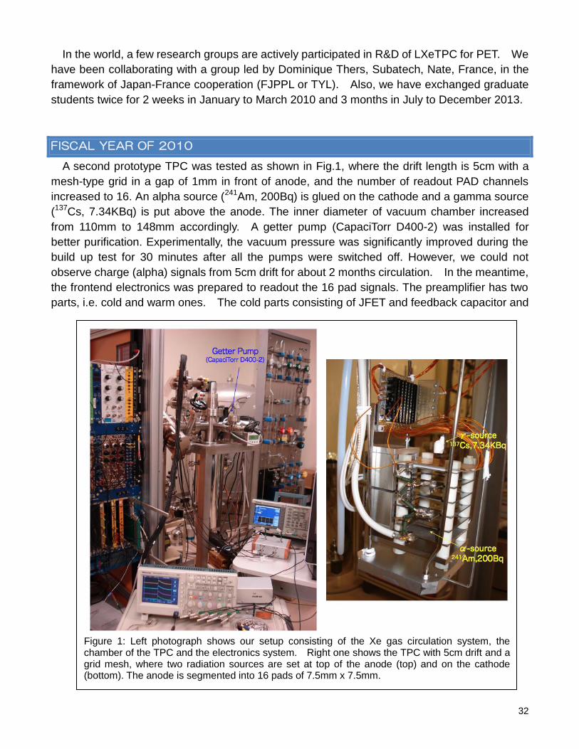
32
In the world, a few research groups are actively participated in R&D of LXeTPC for PET. We
have been collaborating with a group led by Dominique Thers, Subatech, Nate, France, in the
framework of Japan-France cooperation (FJPPL or TYL). Also, we have exchanged graduate
students twice for 2 weeks in January to March 2010 and 3 months in July to December 2013.
FISCAL YEAR OF 2010
A second prototype TPC was tested as shown in Fig.1, where the drift length is 5cm with a
mesh-type grid in a gap of 1mm in front of anode, and the number of readout PAD channels
increased to 16. An alpha source (241Am, 200Bq) is glued on the cathode and a gamma source
(137Cs, 7.34KBq) is put above the anode. The inner diameter of vacuum chamber increased
from 110mm to 148mm accordingly. A getter pump (CapaciTorr D400-2) was installed for
better purification. Experimentally, the vacuum pressure was significantly improved during the
build up test for 30 minutes after all the pumps were switched off. However, we could not
observe charge (alpha) signals from 5cm drift for about 2 months circulation. In the meantime,
the frontend electronics was prepared to readout the 16 pad signals. The preamplifier has two
parts, i.e. cold and warm ones. The cold parts consisting of JFET and feedback capacitor and
Figure 1: Left photograph shows our setup consisting of the Xe gas circulation system, the chamber of the TPC and the electronics system. Right one shows the TPC with 5cm drift and a grid mesh, where two radiation sources are set at top of the anode (top) and on the cathode (bottom). The anode is segmented into 16 pads of 7.5mm x 7.5mm.
33
resistor were installed in the chamber at liquid Xe temperature, while the warm parts are made
on a PC board fitted in the NIM module. Shaping the outputs of the preamplifier, signals were
digitized by flash ADC CAMAC modules with 20MHz. Cosmic ray events are analyzed with the
16 pads, even if the alpha signals are difficult to be detected. Scintillation lights are read out by
500MHz FADCs for the PSD (Pulse Shape Discrimination) analysis. Performance of
purification is studied also in Xe gas phase for the quantitative evaluation.
FISCAL YEAR OF 2011
First, there was no damage by the Great Eastern Japan Earthquake, March 11, 2011, while a
digital oscilloscope and a desktop personal computer fell down from the table.
In this fiscal year, following three major efforts have been conducted, that is (1) a test of the
TPC prototype with 5cm drift and 16ch pad readout, (2) strength test of a ceramic end plate and
(3) development of ASIC front-end electronics.
One of major issues for the TPC prototype test is a purification of liquid xenon in the chamber.
Since the xenon gas is purified in circulating through the getter, one immediate possibility is to
increase the flow rate for efficient purification. The flow rate is limited by the cooling power of
the pulse tube refrigerator (PTR, PDC08 of Iwatani co.). Therefore, we upgrade a helium
compressor of the PTR. Actually, the cooling power was increased from 21W to 31W at 165K,
where the flow rate can be raised from 0.4L/min to 2L/min. However, we could not keep the
cooling power and we have frequently had to warm up and unfreeze the cold head of PTR for 3
months. This problem was finally solved by installation of a molecular sieve adsorption vessel at
the compressor discharge side to clean up the helium gas, September 2011. Since then, we
could operate the PTR at the flow rate of 1.4 to 1.8L/min. After the purification for 2 weeks, the
charge signal has been observed just one time, 6th October 2011. It has been a mystery why
Figure 2 : The strength test of a ceramic endplate : Left photograph shows a water leak in a circle at about 20 atm. of the water pressure. Right figure shows a ceramic plate glued on the ICF152 SUS flange, where the water pressure is applied from right hand side. Unit is mm.
34
the observation was just one time. Finally, we found that it was due to a lower liquid level of
xenon in the chamber, February 2012. For the moment, the level must be higher about 4cm
than the TPC anode at least, where the charge (electrons) drifts upward.
We had a strength test of a ceramic endplate for next prototype with front-end electronics at
the endplate, April 2011, as shown in Fig. 2. The ceramic plate has area of 5cm x 5cm with
3.5mm thickness. The plate is glued on the SUS flange with STYCAST. It was gradually
pressured by water up to 35 atm. for about 8 minutes. We observed a small water leakage at
about 20 atm. So, it shows enough strength at least at room temperature.
The ASIC front-end electronics has been developed recently in a framework of the Open-IT.
We tested a TPCFE09 chip (second version) with 16 channels/chip both at room temperature
(300K) and 165K. So, it was shown to work at the liquid xenon temperature. The gain and
noise were measured to be 10-13V/pC and 1,200-1,650 electrons (ENC), respectively.
FISCAL YEAR OF 2012
In this fiscal year (2012), we have succeeded to operate the prototype TPC filled with liquid
Xe since August, 2012 until end of March, 2013. As shown in Figure 3, the TPC has 5cm drift
in the electric field of 0.5 kV/cm with a grid of 1mm gap (2.6kV/cm), where the anode consists of
16 pads in a 4x4 matrix configuration. First, charge signals are detected by pre-amplifiers
connected to each pad in the chamber followed by shaping amplifiers in room temperature.
They are digitized by the 20MHz Flash ADC (CAMAC modules). All 16 channels have been
alive and monitored by test pulses. In the chamber, two alpha sources, α1 and α2 of 241Am
are set on a wire stretched at 1cm from the anode and on the cathode plane, respectively. A
gamma-ray source of 137Cs is also installed on top of the anode (Figure 3). Two
photo-multipliers provide trigger signals from the scintillation lights. The liquid Xe of about 2.5
liters was purified by circulation with the gas flow of about 1.3liters/min. The purification process
was monitored by the total charges of signals from the three sources. The total charges
rapidly increased for a month followed with saturation. For sufficient gas flow, the cold head of
pulse tube refrigerator was warmed up every morning with recovery of the cooling power by
40% for about 3 months. The total charges resumed the increase gradually followed with
saturation again. The electron lifetimes until capturing in impurities have been measured by
gammas during these purification process and the saturation states (Figure 4). Basic properties
such as the electron drift velocity and the grid transparency were also measured as a function of
applied electric fields. As shown in Figure 4, the maximum lifetime was 77± 7usec
corresponding to the attenuation length of 12±1cm. The oxygen equivalent concentration of
impurities was estimated to be about 6ppb, while the target value is less than 1ppb.
35
Figure 3 : TPC prototype chamber with 5cm drift. Level of liquid Xe was over 15cm of the gauge during operation in 2012. Right graph shows the growth of charge signals of the second alpha source α2, from 23 August to end of March 2013. profile line.
Figure 4 : Charge signals of gamma's selected by the scintillation lights during the saturation
period in 2012.12.10 through 2013.1.19 : Left shows a scatter plot of charge signals in a plane
of the pulse height and the drift time. Right shows the average and RMS of the pulse heights
as a function of the drift time.
36
FPIX PROJECT
KISHIMOTO, Syunji
OVERVIEW
The FPIX project has been developing a frontend circuitry for a silicon avalanche photodiode
(Si-APD) array detector for time-resolved measurements using pulsed synchrotron X-rays since
FY2010. The Si-APD detector has 64 pixels in a linear array. Each pixel is 100 mm ×200 mm,
with a thickness of 10 mm. A 50-mm gap separates adjacent pixels in the array, resulting in a
total sensitive region length of 9.6 mm. The time resolution ΔT (FWHM) is expected to be 100
ps for X-rays, based on the device thickness. In order to apply the APD detector to
time-resolved diffraction measurements with 2 ns pulse-pair resolving time and a count rate of
up to 108 s–1, a four-channel ASIC, 4 mm × 4 mm in size, was fabricated for processing a
nanosecond-width pulse from each pixel of the Si-APD in FY2010. The ASIC consists of a
current amplifier with a baseline restorer, a comparator, and T-flip flops, as shown in the block
diagram in Fig. 1. The output signals from the ASIC are fed at a rate of 125 MHz into an FPGA
circuit.
In FY2011, a test board of 64-channel fast pulse electronics was developed using the
front-end ASICs fabricated in FY2010. The 64-channel Si-APD linear array was mounted on
the test board and the 64-channel X-ray detector was tested using 8-keV X-ray beam at
beamline BL-14A of Photon Factory (PF).
Fig.1 Block diagram of ASIC for Si-APD array detector
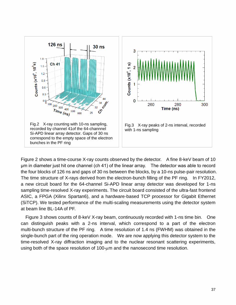
37
Figure 2 shows a time-course X-ray counts observed by the detector. A fine 8-keV beam of 10
μm in diameter just hit one channel (ch 41) of the linear array. The detector was able to record
the four blocks of 126 ns and gaps of 30 ns between the blocks, by a 10-ns pulse-pair resolution.
The time structure of X-rays derived from the electron-bunch filling of the PF ring. In FY2012,
a new circuit board for the 64-channel Si-APD linear array detector was developed for 1-ns
sampling time-resolved X-ray experiments. The circuit board consisted of the ultra-fast frontend
ASIC, a FPGA (Xilinx Spartan6), and a hardware-based TCP processor for Gigabit Ethernet
(SiTCP). We tested performance of the multi-scaling measurements using the detector system
at beam line BL-14A of PF.
Figure 3 shows counts of 8-keV X-ray beam, continuously recorded with 1-ns time bin. One
can distinguish peaks with a 2-ns interval, which correspond to a part of the electron
multi-bunch structure of the PF ring. A time resolution of 1.4 ns (FWHM) was obtained in the
single-bunch part of the ring operation mode. We are now applying this detector system to the
time-resolved X-ray diffraction imaging and to the nuclear resonant scattering experiments,
using both of the space resolution of 100-m and the nanosecond time resolution.
Fig.2 X-ray counting with 10-ns sampling, recorded by channel 41of the 64-channnel Si-APD linear array detector. Gaps of 30 ns correspond to the empty space of the electron bunches in the PF ring
Fig.3 X-ray peaks of 2-ns interval, recorded with 1-ns sampling
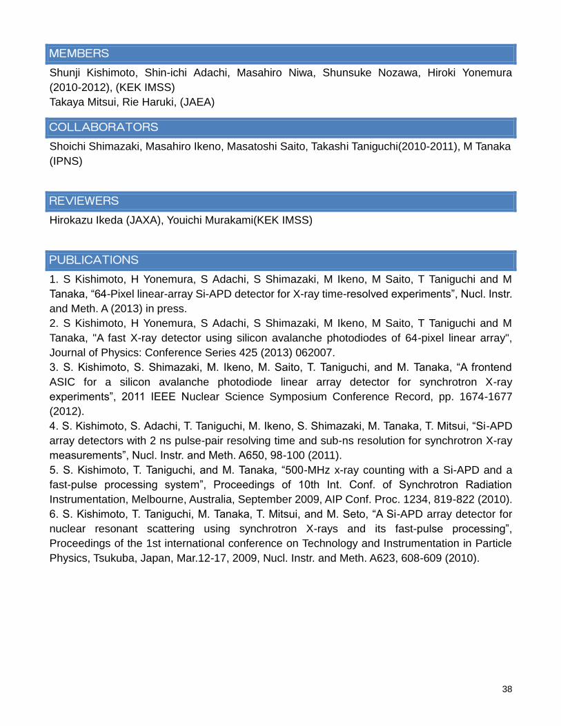
38
MEMBERS
Shunji Kishimoto, Shin-ichi Adachi, Masahiro Niwa, Shunsuke Nozawa, Hiroki Yonemura
(2010-2012), (KEK IMSS)
Takaya Mitsui, Rie Haruki, (JAEA)
COLLABORATORS
Shoichi Shimazaki, Masahiro Ikeno, Masatoshi Saito, Takashi Taniguchi(2010-2011), M Tanaka
(IPNS)
REVIEWERS
Hirokazu Ikeda (JAXA), Youichi Murakami(KEK IMSS)
PUBLICATIONS
1. S Kishimoto, H Yonemura, S Adachi, S Shimazaki, M Ikeno, M Saito, T Taniguchi and M
Tanaka, “64-Pixel linear-array Si-APD detector for X-ray time-resolved experiments”, Nucl. Instr.
and Meth. A (2013) in press.
2. S Kishimoto, H Yonemura, S Adachi, S Shimazaki, M Ikeno, M Saito, T Taniguchi and M
Tanaka, "A fast X-ray detector using silicon avalanche photodiodes of 64-pixel linear array",
Journal of Physics: Conference Series 425 (2013) 062007.
3. S. Kishimoto, S. Shimazaki, M. Ikeno, M. Saito, T. Taniguchi, and M. Tanaka, “A frontend
ASIC for a silicon avalanche photodiode linear array detector for synchrotron X-ray
experiments”, 2011 IEEE Nuclear Science Symposium Conference Record, pp. 1674-1677
(2012).
4. S. Kishimoto, S. Adachi, T. Taniguchi, M. Ikeno, S. Shimazaki, M. Tanaka, T. Mitsui, “Si-APD
array detectors with 2 ns pulse-pair resolving time and sub-ns resolution for synchrotron X-ray
measurements”, Nucl. Instr. and Meth. A650, 98-100 (2011).
5. S. Kishimoto, T. Taniguchi, and M. Tanaka, “500-MHz x-ray counting with a Si-APD and a
fast-pulse processing system”, Proceedings of 10th Int. Conf. of Synchrotron Radiation
Instrumentation, Melbourne, Australia, September 2009, AIP Conf. Proc. 1234, 819-822 (2010).
6. S. Kishimoto, T. Taniguchi, M. Tanaka, T. Mitsui, and M. Seto, “A Si-APD array detector for
nuclear resonant scattering using synchrotron X-rays and its fast-pulse processing”,
Proceedings of the 1st international conference on Technology and Instrumentation in Particle
Physics, Tsukuba, Japan, Mar.12-17, 2009, Nucl. Instr. and Meth. A623, 608-609 (2010).
39
ASIC PROJECT
TANAKA, Manobu
OVERVIEW
The ASIC project aims to increase the activity of ASIC development for sensors in the high
energy physics experiments and the experiments in the related fields.
Resources(i.e. man power and know-how) of the ASIC design are accumulated by following
processes.
1. Development of several ASICs 2. Education based on the accumulated know-how
The first step for the item 1 was supported by KEK-DTP for several years, then several
projects have developed ASICs, and we accumulated know-how of the development. The
second has been subsidized by a KEK support program for accelerator science and technology.
We’ve successfully established a collaboration network for ASIC development with experts in
JAXA, NIAS, TITec and KEK-IPNS. Until now 21 ASIC development projects, e.g. a silicon trip
detector readout ASIC, a GEM foil readout ASIC and MPPC readout ASIC, were started and the
eleven of the projects(ref.1~11) were completed.
After the education program launched, we started development of QPIX in collaboration with
Tokyo Institute of Technology(TITec), Saga University, Kobe University, Nagasaki Institute of
Applied Science and KEK to perform followings.
1. Development of the higher density and sophisticated frontend electronics. 2. Development of interposer and integration technique. 3. Integration as a gas-based pixel detector.
Those developments are necessary for the next generation time projection chamber (TPC).
The basic elements used in the QPIX have been developed and the functions are confirmed.
After a graduate student left from TITec, KEK has taken over the develpment in the middle of
2013. Low temperature co-fired ceramics (LTCC) as an interposer technique was evaluated and
confirmed as a promising technique for development of large area TPCs and/or a gas pixel
detectors from the view point of reliability at present. We also successfully observed heavy ion
tracks and evaluated the tracking performance.
We will continue the development effort to establish “depth and breadth” collaboration
network.
In the following sections details of the ASIC development and QPIX development are
described.
I ASIC DEVELOPMENT
Figure 1 shows examples of technology inheritance from the ASIC project to several
experiments. After we developed a frontend ASIC for micro pattern gas detector (MPGD) using
CMOS 0.5um for three years, in the CMOS 0.5um case all chips shown in Figure 2 are
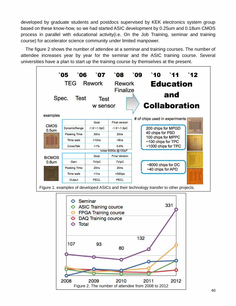
40
developed by graduate students and postdocs supervised by KEK electronics system group
based on these know-how, so we had started ASIC development by 0.25um and 0.18um CMOS
process in parallel with educational activity(i.e. On the Job Training, seminar and training
course) for accelerator science community under limited manpower.
The figure 2 shows the number of attendee at a seminar and training courses. The number of
attendee increases year by year for the seminar and the ASIC training course. Several
universities have a plan to start up the training course by themselves at the present.
Figure 2. The number of attendee from 2008 to 2012
Figure 1. examples of developed ASICs and their technology transfer to other projects.
41
I I QPIX DEVELOPMENT
We have been developing a gas pixel
detector as a charged particle tracking
device to accumulate design know-how of
higher integrated and more complex readout
electronics. Each pixel has a frontend
electronics, ADC for dE/dx measurement
and TDC for Time-Of-Flight (TOF)
measurement. The QPIX measures a
charged particle track by the x-y position of
the pixel and the z position by the TOF, and
the energy deposit (Q) is measured by ADC
as shown in Figure 3.
A Time-Over-Threshold (TOT) counter is
employed for dE/dx measurement in other
ASIC developments, but the TOT depends
on the particle incidence angle to the QPIX.
(e.g. TOT of a perpendicular track is smaller
than that of a parallel track to the TPC
electric field.) Therefore we employ ADC for
dE/dx measurement.
There are three R&D items as follows 1. The pixel ASIC development. 2. Interposer development for
connections between charge collection pixel electrodes and the pixel ASIC.
3. Integration and evaluation of the three dimensional tracking device.
The three R&D items are done by the
QPIX collaboration (Tokyo Institue of
Technology, Saga Univ, Kobe Univ,
Nagasaki Institute of Applied Science and
KEK IPNS).
Details are described in the following
sections.
II-1 Pixel design
We have submitted two versions of QPIX-v0 and QPIX-v1 using TSMC0.18umCMOS 1P6M.
Figure 3 Basic function of QPIX
Table 1 Specifications of QPIX-v0 and QPIX-v1
42
Those specifications are listed in Table 1. QPIX-v0 is the first prototype chip designed,
Figure 4 Block diagram of the QPIX-v1, a pixel cell and its layout
Figure 5 TOF and TOT performance in the test bench
Figure 6 SAR ADC test result (left) using the test pulse input and the result (right) using charge collection pad

43
fabricated and characterized for basic
function validation. QPIX-v0 has issues (i.e.
the number of pixel, no readout control
circuit for large amount of registers and no
offset calibration circuit in amplifiers and
comparators.).
QPIX-v1 is designed to overcome those
issues.
Figure 4 shows the schematic of a pixel
cell in QPIX-v1 and its layout. It is composed
of two main blocks: the analog block
consisting of the amplifier, the integrator, the
comparator and the SAR ADC; and the
digital block mainly consisting of the pixel
control logic, the 14-bit Time-of-Flight (TOF)
counter, the 10-bit ADC resister and the 8-bit
Time-over-Threshold (TOT) register. The
system clock of 100MHz determines the
timing resolution of TOF and TOT. The pixel
size is 200um x 200um, and the size of
active circuit area is 130 um times 140um.
The electrical measurement of a pixel in
QPIX-v1 in a test bench is shown in Figure 5
and 6.
We confirmed TOF and TOT counters
measured the timing with 10ns accuracy.
The ADC codes show that the
monotonicity can be kept; however there is
an offset of 0.6pC for the input range. The
large parasitic capacitance in the test input
line, which is totally 49pF, was connected to
the input of the transe impedance amplifier
(TIA) in Figure 4. The gate timing of the
integrator in the SAR ADC is determined by
the leading edge of the TIA output. Since the
leading edge timing is delayed by the
Figure 7 Intrinsic noise of the QPIX. The red circle indicates Spectre simulation results, and the black circle is the measurement.
Figure 8 Photos of charge collection pads and the backside connected to PCB. The lower picture shows the cross section of the LTCC structure.
44
additional capacitance, the ADC offset is
caused by the timing shift. Figure 6 shows
the ADC count as the function of the input
charge which is directly injected at input pad.
The offset becomes smaller than 0.6pC
shown in Figure6. The problem will be
solved by adding frontend circuit in between
a pad and a current integrator.
The intrinsic noise is measured and
compared to the simulation as shown in
Figure 7. The intrinsic noise is small enough
at typical detector capacitance of 1pF.
II-2 Interposer development
There are several technology choices for
the interposer development. From the
viewpoint of production cost and feasibility
we choose low temperature co-fired ceramic
(LTCC).
Figure 8 shows the 16 layers LTCC
interposer. The interposer has 20 x 20
charge collection pads. The size of the
charge collection pad is 460um x 460um and
the pitch is 540um. The readout side has 88
solder ball whose diameter is 500um and the
pitch is 0.8mm. The size of the charge
collection pad on the QPIX-v1 is 70um x
70um, and the pitch is 200um. The pad for
IO and power supply are located around the
20 x 20 charge collection pads array, and the pas size is 90um x 90um and the pitch is 150um.
The first prototype has warpage of the flip-chip bonding surface on the LTCC. It was in between
40um and 60um depends on the products. After modification of the mechanical structure, we
achieved the surface flatness less than 30um. The geometry measurement result is shown in
Figure 9. The production yield using second LTCC samples becomes 100% for 3360
connections. All samples are working. We measured resistance distribution of the connection
showed in Figure 10. The resistance variation is less than 200Ohm.
Figure 10 Resistance distribution of connection for typical sample. The resistance value includes resistance of analog switch.
Figure 9 The geometry measurement of bonding surface
45
II-3 System integration as a charged particle tracking device
The structure of the time projection chamber (TPC) using QPIX is shown in Figure 11. The
drift space is 2.8 cm, and we use three layers of GEM for electron amplification. The HV for
GEM is 340V each. We developed another interposer for evaluation of the TPC using QPIX in
parallel with R&D of LTCC development for large area TPC. We adopted the wire-bonding
integration technology. The package is shown in Figure 11. A cover protects wire bonding and
corrects the shape of the electric field in the induction region.
Heavy ion beam at Takasaki JAEA is used for a demonstration of three dimensional tracking
and the evaluation of the TPC performance. Figure 12 shows a beam track and the resolution.
Figure 11 Cross section of the QPIX TPC and the pictures. Left bottom pictures are another LTCC interposer with wire bonded QPIX without a metal cover and without metal cover.
Figure 12 Track of the heavy ion beam and the TPC position resolution

46
REFERENCE (FROM 2010 RELATED TO THE QPIX PROJECT)
Grant-in-Aid
1. Grant-in-Aid for Young Scientists(A) H23-26 21700k yen Kentaro Miuchi 2. Grant-in-Aid for Scientific Research(B) H21-23 14000k yen Akira Sugiyama 3. Grant-in-Aid for Exploratory Research H23-24 2,900k yen Kentaro Miuchi
Publication
1. Akira Matsuzawa, Vu Minh Khoa, Fei Li, Masaya Miyahara, Takashi Kurashina, "A new particle detector LSI, Qpix :Integrating high speed ADC for each pixel," Nuclear Inst. and Methods in Physics Research, A623(2010), Volume 623, Issue 1, pp. 477-479, Nov. 2010.
2. “Qpix v.1: A high speed 400-pixels readout LSI with 10-bit 10 MSps pixel ADCs”, Fei Li, et al., Nuclear Instruments and Methods in Physics Research, A650, Issue 1, pp. 101-105, Sep. 2011.
3. "NEWAGE" K. Miuchi, K. Nakamura, A. Takada, S. Iwaki, H. Kubo, T. Mizumoto, H. Nishimura, J. Parker, T. Sawano, T. Tanimori, H. Sekiya, A. Takeda, T. Fusayasu, A. Sugiyama and M. Tanaka Proceedings of "CYGNUS 2011 : 3rd Workshop on directional detection of Dark Matter" Aussois, France, June 8-10, 2011 EAS publication Series 53 (2012) pp. 33-41, 1109.3099 DOI:10.1051/eas/0936034
4. “A Low-Noise High-Dynamic Range Charge Sensitive Amplifier for Gas Particle Detector Pixel Readout LSIs,” Fei Li et al., IEICE Transactions on Electronics, conditionally accepted and expected be published in 2013.
Presentation(International conference and workshop)
1. “A new particle detector LSI Qpix: integrating high speed ADC for each pixel”
Akira MATSUZAWA (oral presentation) TIPP 2009, Tsukuba, Japan
2. “QPIX v.1:A High Speed 400-pixels Readout LSI with 10-bits 10Msps Pixel ADCs,”
Internatinal Workshop on Millimeter Wave Wireless Technology and Applications, Tokyo,
Japan, Dec. 2010
3. Fei Li, Vu Minh Khoa, Masaya Miyahara and Akira Matsuzawa, "Qpix v.1: A High Speed
400-pixels Readout LSI with 10-bit 10MSps Pixel ADCs," PIXEL2010 International Workshop,
Grindelward, Switzerland, Sep. 6 - 10, 2010
4. "R&D of QPIX", Akira Sugiyama CYGNUS 2013(oral persentaion)Toyama, Japan June 11,
2013

47
Presentation(Domestic conference and workshop)
1. "QPIX" K. Miuchi 7thMPGD workshop@Yamagata Univ. 2010/11/26
2. "QPIX" K. Nakashima 8thMPGD workshop@Kinki Univ. 2011/12/9
3. "QPIX beam test results" R. Miyashita 9thMPGD workshop@NIAS 2012/12/7
4. "Development of MPGD using a buildup method" K. Miuchi 9thMPGD
workshop@NIAS 2012/12/7
Doctor Thesis
1. “Quasi-3D Pixel Readout LSIs for Gaseous Particle Detectors”,
Fei Li 2012 Tokyo Institute of Technology
Master Thesis
2. “A pixel readout LSI with a built-in ADC for particle detector applications”
Vu Minh Khoa 2010 Tokyo Institute of Technology
3. “Development of a gas pixel detector”, Kenichi Nakashima 2011 Saga Univ.
------------------------------------------------------------------------------------------------------------------------
ref1. Development of wide range charge integration application specified integrated circuit for photo-sensor, NIMA, vol 699, p.124-128 ref2. Development of a tracking detector system with multichannel scintillation fibers and PPD, NIMA vol695p.206-209 ref3. A frontend ASIC for a silicon avalanche photodiode linear array detector for synchrotron X-ray experiments, IEEE NSS CR(2012)p.1674-1677 ref4. Front-end electronics of the Belle-II drift chamber, NIMA vol735p.193-197 ref5. Development of a wide-dynamic range Front-End ASIC for W+Si calorometer,IEEE NSS CR(2012)p576-580 ref6. Development of a Time-resolved neutron imaging detector based on the uPIC micro-pixel chamber, NIMA,vol689p.23-31 ref7.Development of an amplifier IC with wide dynamic range for Si detector in Riken Samurai spectrometer, IEEE NSS CR(2012)p854-857 ref8.Development of frontend electronics for LEPS2-TPC, Keigo Mizutani, 2012 Master Thesis ref9.ASIC design and fabrication for frontend electronics of liquid xenon TPC, TIPP09 poster presentation T. Higashi ref10..radiation tolerant ASIC development for muon TGC trigger system upgrade, Shuji Shichi 2011 Master Thesis ref11. The development of time projection chamber frontend ASIC for the Neutron Lifetime Measurement, IEEE NSS 2013 poster presentation H. Yokoyama
48
CO2 PROJECT(TWO-PHASE CO2 COOLING SYSTEM)
SUGIMOTO, Yasuhiro
INTRODUCTION
One of the characteristics of recent detector systems for high energy physics experiments is
the high density implementation of readout electronics on the sub-detectors. Power
consumption of these readout electronics is quite large, and efficient and low material cooling
system is indispensable. Silicon strip sensors and silicon pixel sensors often require low
temperature operation to reduce the dark current caused by radiation damage. The cooling
system is an important element of detectors using these sensors, as well. For these purposes,
detector cooling systems using 2-phase CO2 as the coolant are attracting attentions recently.
Detector cooling systems using 2-phase fluid which utilizes latent heat of the fluid have been
used for several advanced detector systems such as ATLAS SCT. Because cooling systems
using 2-phase fluid utilize large latent heat, they need much less flow rate of the coolant
compared with the cooling system using water as the coolant. The heat load is consumed only
for phase transition, and the cooling with constant temperature everywhere along the cooling
tube can be achieved in 2-phase cooling systems.
Two-phase coolant which has been widely used for detector cooling such as ATLAS SCT is
perfluorocarbon (PFC) CnF2n+2. Compared with PFC, CO2 has much larger latent heat as shown
in Table 1, and still less flow rate is necessary. Because 2-phase CO2 is used at higher pressure
(1 MPa at −40°C and 5 MPa at 15°C), the evaporated vapor volume is less, and relative
pressure drop along the tube is less than PFC. Thanks to these characteristics, we can use
thinner cooling tube for CO2 than PFC, and total material budget including the cooling tube and
the coolant is less for CO2 cooling systems. Low material budget is a crucial issue to suppress
multiple scattering of charged particles and to improve the momentum resolution of the
detector.
So far, 2-phase CO2 cooling system has been successfully used for AMS tracker [1],
LHCb-VELO [2], etc., which have been developed mainly by NIKHEF. Recently, R&D groups for
2-phase CO2 cooling have been started in several laboratories such as CERN, FNAL, and
SLAC, mainly for the application to the LHC detector upgrade. We have started R&D of 2-phase
CO2 cooling system also in KEK. Our goal is to develop a test system of 2-phase CO2 cooling
which can be applied for detector cooling between −40°C and near room temperature, and to
accumulate technique and know-how of the 2-phase CO2 cooling system in KEK. One big
contrast of our R&D effort to other groups is that we are aiming at developing a 2-phase CO2
cooling system using a gas compressor for CO2 circulation, while other R&D groups use liquid
pumps for CO2 circulation.

49
Our group consists of members who are working on ILC TPC, ILC vertex detector, Belle-II
vertex detector, and KEK cryogenic group. The required cooling temperature ranges from
−40°C to near room temperature. However, one 2-phase CO2 cooling system can cover all the
temperature range.
Table 1. Characteristics of coolant
BLOW SYSTEM
Before developing a circulating cooling
system, we have constructed a so-called
“blow system” in which CO2 does not
circulate but blows off after cooling a heat
source. The schematic diagram is shown in
Figure 1. At the beginning, liquid CO2 from
a CO2 bottle is depressurized by a needle
valve, and temperature goes down due to
Jule-Thomson effect. The temperature after
the expansion is determined by the
pressure which is set by a back-pressure
regulator. After cooling a dummy detector,
the 2-phase CO2 is used to pre-cool the
incoming CO2 at a heat exchanger. At the
equilibrium state, the temperature drop of
the incoming CO2 is dominated by the heat
exchange at this heat exchanger, not by the
J-T expansion (see Figure 2). The 2-phase
CO2 is completely evaporated by a heater,
and exhausted to the environment through
the back-pressure regulator. Phase
diagram of this system is shown in Figure 2.
The state at each point of 1 – 8 in Figure 1 can be found in Figure 2. At the beginning of the
operation, the state transition of 123’4’78 occurs in Figure 2. At the equilibrium state,
the transition of 12345678 happens.
The actual system is equipped with many pressure gauges, temperature sensors, safety
valves, and a flow meter. Photograph of the system is shown in Figure 3. With this extremely
CO2 C2F6 C3F8
Latent heat (at −40°C) 321 J/g ~100 J/g ~110 J/g
Triple point −56.4°C −97.2°C −160°C
Critical point 31.1°C 19.7°C 71.9°C
Figure 1. Blow system
Heater
Needle valve
Back pressure
regulator
Dummy
detector
CO2 bottle
Heat
exchanger
① ②
③④
⑤
⑥
⑦
⑧
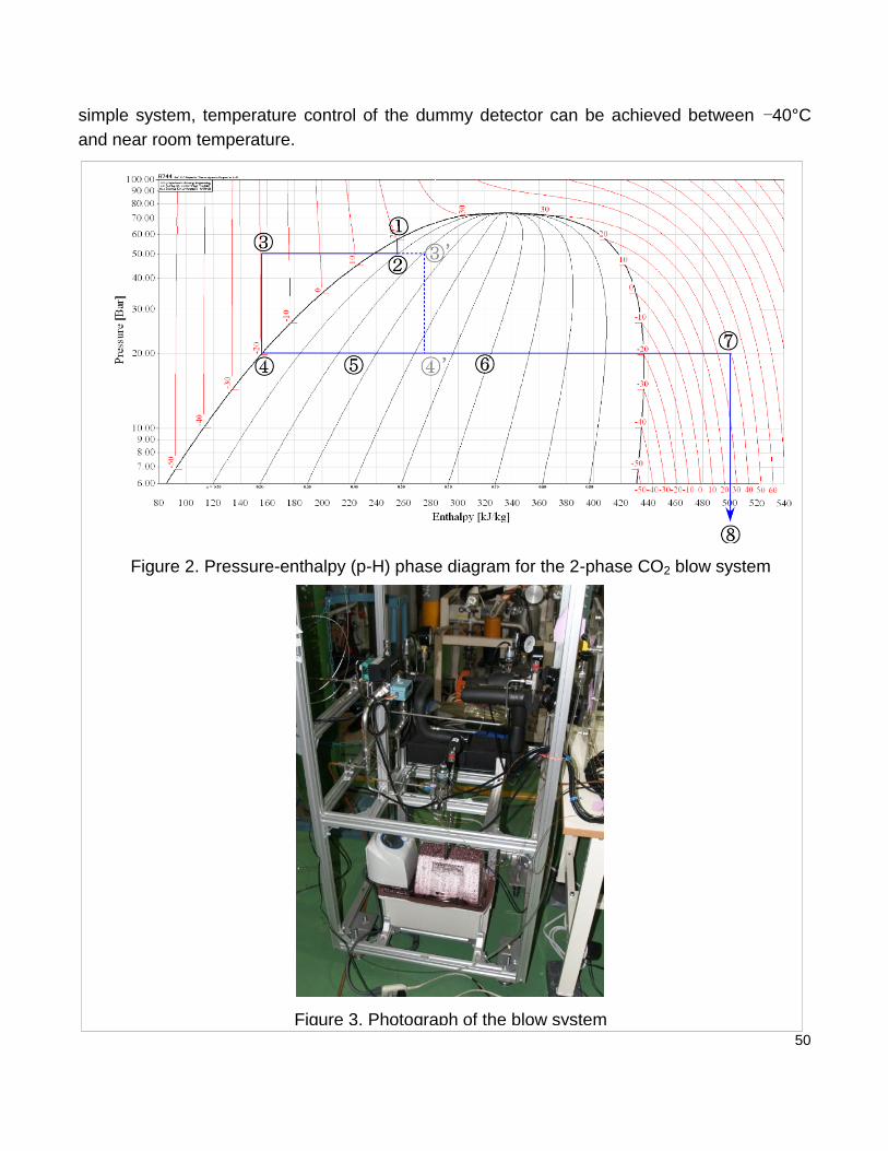
50
simple system, temperature control of the dummy detector can be achieved between −40°C
and near room temperature.
Figure 2. Pressure-enthalpy (p-H) phase diagram for the 2-phase CO2 blow system
Figure 3. Photograph of the blow system

51
CIRCULATING SYSTEM
Inspired by the successful operation of the very simple blow system, we have started R&D of
a circulating cooling system using a gas compressor for circulation, which is straight extension
of the blow system. If CO2 gas which is exhausted in the blow system is compressed and
condensed to liquid again, it becomes a circulating system. Schematic diagrams of circulating
systems using a liquid pump and a gas compressor are shown in Figure 4.
Figure 4. Simplified schematic diagrams of circulating cooling systems using a liquid
pump (top) and a gas compressor (bottom).
CO2
Chiller
Condenser
Heat exchanger
Needle valve
Detector
-40~20℃
Liquid pump
Pressure
control
system
2-phase accumulator
CO2
Chiller Condenser
Back-pressure
valve
Heat exchanger
Needle valve
Detector
Heater
5~20℃
Compressor

52
In the cooling system using a liquid pump, the temperature of the 2-phase CO2 is determined
by the pressure controlled by the 2-phase accumulator. Temperature of the liquid CO2 at the
outlet of the condenser is below the saturation temperature. If we want to cool the detector at
−40°C, the chiller has to supply the coolant of below −40°C to the condenser. The liquid CO2
transferred between the cooling plant and the detector has a temperature equal to or below the
cooling temperature of the detector. Usually, a detector is located at a long distance from the
cooling plant, and tight thermal insulation of the transfer tube for the liquid CO2 is necessary to
suppress the heat load.
In the cooling system using a gas compressor, on the contrary, the operating temperature of
the chiller is close to the room temperature. Liquid CO2 close to the room temperature is
transferred between the plant and the detector.
Table 2 summarizes the characteristics of the cooling system using a liquid pump and a gas
compressor. Although it seems that the cooling system using a gas compressor has advantages
over the cooling system using a liquid pump, most of the high energy physics experiments using
2-phase CO2 cooling system have employed the system using a liquid pump. The main reason
is that they could not find a good oil-free compressor which can compress the gas to quite high
pressure required by the CO2 system.
Table 2. Comparison of cooling systems using a liquid pump and a gas compressor
Liquid pump Gas compressor
Temp. of pump/compressor Low (<Tdetetcor) High
Temp. of condenser Low (<Tdetetcor) ~ Room temperature
Temp. of transfer tube:
plantdetetor
Low (<Tdetetcor) ~ Room temperature
Temp. of transfer tube:
detectorplant
Low (=Tdetector)
(Liquid (2-phase))
~ Room temperature
(Gas)
We have designed a circulating CO2 cooling system using a gas booster as the gas
compressor. The gas booster we employed is model AGD-7 of Haskel. The gas booster is an
oil-free reciprocal compressor driven by high pressure air. This air is also used for cooling of the
gas booster. The maximum pressure obtained by AGD-7 is PO=7PA+PS, where PA is the driving
air pressure and PS is the suction gas pressure.
Figure 5 shows the schematic flow diagram of the system. Relatively low pressure CO2 gas is
compressed by the gas booster. The driving air is supplied by a air compressor (Anest Iwata,

53
SLP-37EEDM5) which can deliver air of 410 L/min (ANR). High pressure CO2 gas is cooled by
cooling water supplied by the chiller and liquefied at the condenser. The liquid CO2 is
transferred to the heat exchanger and cooled down close to the cooling temperature. Then, CO2
is de-pressurized by the needle valve to the pressure determined by the back-pressure valve.
Liquid CO2 evaporates to some extent through the detector and the heat exchanger, and is
completely vaporized by the heater, and goes back to the gas booster through the
back-pressure valve. In order to reduce the pulsation due to the reciprocal motion of the gas
booster, two buffer tanks and a pressure regulator is inserted in the circuit. We plan to use this
system for cooling test of detectors between −40°C and +15°C. Parameters expected in the
operation at −40°C and +15°C are given in Table 3. For these two cases, the phase diagram is
shown in Figure 6. The points numbered by 1 – 7 in Figure 6 correspond to the state at the
points numbered by 1 – 7 in Figure 5.
Table 3. Expected operation parameters of the system at −40°C and +15°C
−40°C +15°C
Gas booster suction pressure 0.8 MPa 2.5 MPa
Gas booster discharge pressure 5 MPa 6.6 MPa
Driving air pressure 0.6 MPa 0.6 MPa
Liquefaction temperature at condenser 10°C 20°C
2-phase CO2 pressure 1 MPa 5.1 MPa
2-phase CO2temperature −40°C +15°C
CO2 flow rate 1.3 g/s 5 g/s
System volume ~3.3 L
Charged CO2 ~750 g

54
Figure 6. Pressure-enthalpy (p-H) phase diagram of the cooling cycle for the 2-phase CO2 circulating system for −40°C (L, blue line) and +15°C (H, red line) operation.
L
H
1
23
7
6
5
4
Figure 5. Schematic flow diagram of the circulating CO2 cooling system Right shows the average and RMS of the pulse heights as a function of the drift time.
CO2
Chiller Condenser
BufferBack-pressure
valve
Heat exchanger
Needle valve
Detector
Heater
Driving air-compressor
Pa <0.8 MPa, ~400L/min
Gas boosterAGD-7Po < 7Pa + Ps
5~20℃
Buffer
Flow MeterRegulator
12
3 4
5 6
7

55
The cooling system we have constructed is a system for R&D. Therefore, it is equipped with
pressure gauges, temperature sensors, flow meters, and a dew point sensor at appropriate
positions. In addition, there are several valves for evacuation, ventilation, and safety. The
detailed diagram of the system is shown in Figure 7. In this figure, T, TC, P, D, DM, DI, RU, and
DC stand for Pt temperature sensor, thermo couple, pressure gauge, dew-point sensor,
dew-point monitor, digital indicator, readout unit, and digital controller, respectively. Outputs of
the Pt temperature sensors are directly read out by a data logger. Outputs of other sensors are
converted to either 1~5 V or 4~20 mA signal, and read out by the data logger.
Each buffer has a volume of 1 L, which is much larger than the cylinder volume (216cm3) of
the gas booster. The condenser and the heat exchanger (HEX) are brazed stainless plate heat
exchangers. The area of heat exchanger is 0.64 m2 for the condenser and 0.19 m2 for the HEX.
The dew-point sensor (D) can measure the dew point down to −100°C. Usually, CO2 gas
bypasses the dew-point sensor, and occasionally the dew point is measured by switching the
path by V9. The whole system (inside the dash-dot line box in Figure 7) is housed in a
aluminum frame of 1m(W)×1m(D)×1.8m(H) covered by aluminum panels for safety as shown in
Figure 8.
Assembly of the system has been completed, and we are now in the process of safety
inspection in KEK. Our system has very small cooling capacity (<3 Japanese refrigeration ton),
and is not subject to Japanese safety regulation for high pressure facilities (High Pressure Gas
Safety Act, etc.). However, KEK is keen to safety, and our system is required to satisfy the
regulations.
Figure 7. Detailed diagram of the system.
T
T
F2V5
F4
Chiller
5~20℃
J4
J3
V3
D
Air
compressor
CO2
1/4" (or glued for T)
3/8"1/2"
Electric circuit
P
T
24V
P24V
T
P
24V
DI3 24V DMAC100V
RU24V
T
P 24V
T
T
P
T
P24V DI1
DI224V
T
TCDC
AC100V
AC100V
P24V
GB
Buffer1
Buffer2
J1
J2
J5
J6
J8 J9 J7
Vacuum Vent Vent
V1
V2
V4
V6
V7
V8
V9
V10
V11
RV1RV2
RV3
RV4
RV5
M1
M2
DI424V
DI524V
M4CV
P1
P2
P3
P4
P5
P6P7
F1
Heat bath
M3F3
HEX
DC24VAC100V
Data
Logger
20ch
Interlockcircuit

56
SUMMARY AND PROSPECTS
We have started R&D on 2-phase CO2 cooling system at KEK for cooling of advanced
detectors for high energy physics. At the beginning of the R&D, we constructed a “blow system”
in which CO2 does not circulate. Successful operation of the simple blow system determined us
to develop a circulating CO2 cooling system using a gas compressor instead of a liquid pump.
We have designed and constructed a circulating CO2 cooling system in which a gas booster is
used as the compressor. The system is about to be operated for detailed study.
The present circulating system is for demonstration of feasibility of the system using a gas
booster as the compressor. If it does not work well, we will search another possibility of the gas
compressor. One possible alternative is a compressor used for Eco-cute, a heat pump system
for producing hot water using CO2. If the present system works well, we will develop more
practical systems, such as a system for cooling of remote detector, a more compact system,
and a remote controllable system.
REFERENCES
[1] A.A.M. Delli et al., NLR-TP-2003-001 (2003).
[2] M. Van Beuzekom et al., PoS (Vertex2007) 009 (2007).
Figure 8. Photograph of the system