detector data acquisition hardware designs and features of ngc · figure 2 shows the front panel of...
TRANSCRIPT

Detector Data Acquisition Hardware Designs and
Features of NGC (New General Detector Controller)
Manfred Meyer, Gert Finger European Organisation for Astronomical Research in the Southern Hemisphere, Karl-Schwarzschild-Str. 2, 85748 Garching, Germany Abstract: High performance detectors for astronomy require carefully designed electronics for control
and for data taking. Progress in amplifiers, ADC’s and FPGA technology have made it possible to design compact, scalable, low power and high performance detector data acquisition systems The paper shows important design principles of detector controllers like the set-up of the video chain, monitoring, detector bias and clock generation and clock sequencers. In addition features of the ESO “New General Detector Controller” (NGC) are discussed and how then the primary design is used as a building platform for different applications in the IR and the optical domain, for staring and for real time applications. The NGC platform is used for standard read-outs, as a high speed system or as a pure interface to the first ASIC used for detector control in astronomy.
Key words: detector controllers, data acquisition
1 INTRODUCTION
At DfA2005 a paper about the NGC detector controller [1] was presented (Meyer et al. 2005) describing the basic design and function of a controller based on serial link technology. This paper shows in the first part design principles implemented in NGC, in the second part how out of the design platform other application modules were created extending the functionality of NGC to real time operation, fast data acquisition and interfacing to the SIDECAR ASIC.
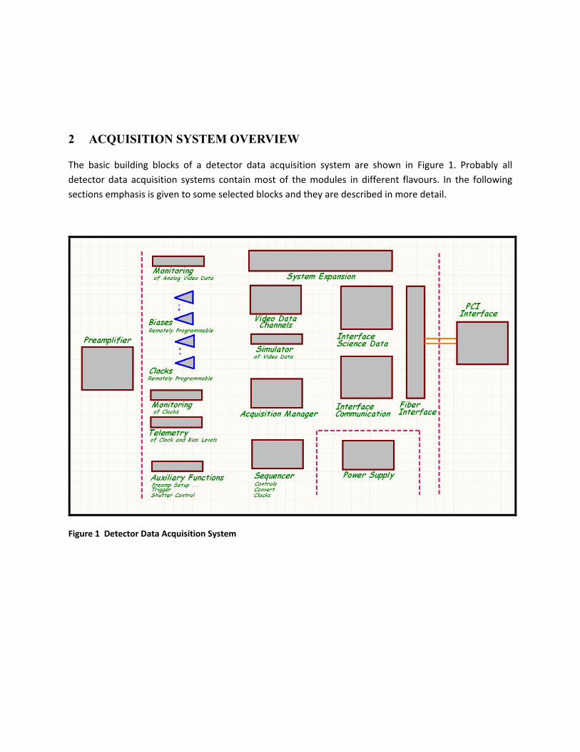
2 ACQUISITION SYSTEM OVERVIEW
The basic building blocks of a detector data acquisition system are shown in Figure 1. Probably all detector data acquisition systems contain most of the modules in different flavours. In the following sections emphasis is given to some selected blocks and they are described in more detail.
Figure 1 Detector Data Acquisition System

2.1 Useful Tools – Telemetry and Monitoring
Before power is applied to a detector it must be certain that all voltages and clocks are correctly set‐up. A telemetry system should give information about voltage levels on biases and clocks, the data acquisition computer compares the measured voltages with the stored references and allows to apply power if everything is in range. It also should be possible to measure telemetry data when the detector is in operation – current measurements on clocks and biases provide additional information about a correctly working system.
Figure 2 shows the Front Panel of the NGC Basic Board with LEMO connectors to monitor via scope the clocks and video signals. Additionally two utility monitors carry selectable sequencer signals for e.g. scope trigger at distinct time points or determination of clamp/sample time. The ADC conversion signal is available on another LEMO. LED’s provide quick look information about system status like link operation, sequencer run, output enable of clocks and biases, conversion signal and system reset. This kind of information is essential especially for maintenance and detector set‐up.
Figure 2 Front Panel NGC Basic Board
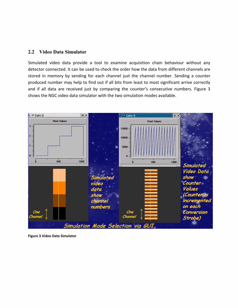
2.2 Video Data Simulator
Simulated video data provide a tool to examine acquisition chain behaviour without any detector connected. It can be used to check the order how the data from different channels are stored in memory by sending for each channel just the channel number. Sending a counter produced number may help to find out if all bits from least to most significant arrive correctly and if all data are received just by comparing the counter’s consecutive numbers. Figure 3 shows the NGC video data simulator with the two simulation modes available.
Figure 3 Video Data Simulator

2.3 The Video Chain
State of the art high resolution ADC’s have fully differential analogue signal inputs. The design concept of the appropriate video amplifier is therefore a completely symmetrical setup. On the positive and the negative video inputs high impedance buffers are followed by switchable low pass filters and their buffers. Both chains are connected to the AD8139 low noise rail to rail differential amplifier feeding the differential ADC inputs. It should be mentioned that the ADC’s operating input voltage is very close to the voltage range – for the 16Bit AD7677 with a 2.5 Volt reference a margin of only 0.25 Volt on each side is not much and requires a careful trim of the whole analogue chain to stay in range and use the full dynamic of the ADC (for the 18Bit AD7674 with a final reference voltage of 4.096 Volt the margin is ~ 0.5 Volt). The AD8139 differential amplifier removes any input common mode voltage and has an offset control to bring the signals into the operating input range of the ADC. To avoid negative voltages at the ADC input terminals causing large currents flowing into the ADC’s input protection circuitry the AD8139 is powered from GND to +5 Volt. The differential gain of the video amplifier is 1. Video chain gain setting should be done as close to the detector as possible namely at the detector preamplifier whereas the low pass filtering should be positioned as close as possible to the ADC.
Figure 4 Video Chain

2.4 Working with High Speed ADC’s
High speed pipelined ADC’s are normally used in communications receivers, ultrasound equipment and so on. They also are useful for detector data acquisition in astronomy. Applications are for example high speed detectors or digital filtering of video signals. Pipelined ADC’s are available in different resolutions and speed grades. The ADC we use (AD9248) has 14Bit resolution and does 40 MSamples/s, converting on each positive clock edge with a pipeline delay of 7 clock cycles.
The ADC clock is derived from the detector clock sequencer because all detector clocks have to run synchronously with the ADC clock. As said before, the ADC converts on each positive clock edge but not all converted digital ADC data are needed. A sequencer generated signal (“Convert”) marks the ADC clock edge of interest, this signal is delayed by 7 ADC clock cycles and gates the desired data into the FPGA video data register (see Figure 5).
Figure 5 High Speed Pipelined ADC

2.5 Simple Thing – Detector Bias Generation
For a long time we had seen low frequency noise in our measurements with H2RG detectors. We thought this was 1/f noise caused by the detector and therefore unavoidable, the RMS was not really affected, but with NGC (Figure 6) the effect was stronger than with IRACE (previous ESO IR data acquisition system) and we looked for the reason.
Figure 6 H2RG Noise
The main difference in the bias generation of the two systems is that NGC uses multi channel DAC’s with a higher noise than the DAC’s of IRACE. The filter and buffers following the DAC (Figure 7) were the same with the exception that smaller footprints of the filter components were used. To beat down the 1/f noise of the DAC we increased the filter time constant from 10us to 1s by inserting a ceramic capacitor of 10uF. The problem seemed to be solved but now the image showed something like very low frequency pumping in the 100ms to 1s range. This effect could be related to thermal effects due to local temperature changes on the capacitor. We then finally replaced the ceramic capacitor with a tantalum type and the effect disappeared. We got quite clean images (Figure 8). The reason is still unclear, because the
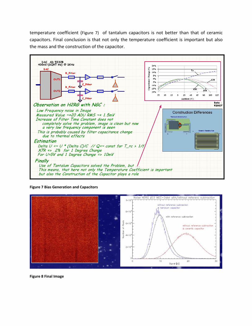
temperature coefficient (Figure 7) of tantalum capacitors is not better than that of ceramic capacitors. Final conclusion is that not only the temperature coefficient is important but also the mass and the construction of the capacitor.
Figure 7 Bias Generation and Capacitors
Figure 8 Final Image

2.6 Sequencer
The most simple sequencer design (Figure 9) is a μController or DSP just writing the clock patterns to an output port. The simple design has the disadvantage that a big memory is needed, timing is related to the program flow and therefore complicated to control, in addition the detector engineer must program the sequencer in a computer language, needs a compiler ..
Figure 9 Most Simple Design of Sequencer
A more elaborated design is shown in Figure 10 . Here only small memories are needed, the sequencer fits easily in a FPGA. There is a memory (SEQ RAM) containing the sequence to be executed and the start addresses of the patterns. Data of this RAM are interpreted by a state machine and just pattern start addresses are written to a FIFO. Another RAM (PATTERN RAM) contains the patterns itself and control bits for “End of Pattern”, the “Read Speed” and the “Number of Repetitions” for a pattern. Logic and a counter for the low addresses complete the design. This sequencer runs fully synchronous, timing is contained in the pattern and the language to program the sequencer is adapted to detector readout. All programming is done in simple syntax and ASCII code. Figure 11 shows the Sequencer Code and the state machine code interpretation time. The uncorrelated readout of a PICNIC array in an infinite loop is shown as an
example in Figure 12.
A more detailed description of the NGC sequencer programming is given in [2].

Figure 10 Sequencer
Figure 11 Sequencer Code and Code Interpretation Time
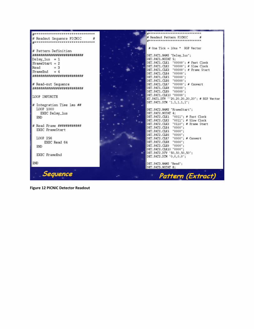
Figure 12 PICNIC Detector Readout

3 NGC SYSTEM
A NGC system consists of two main groups of modules (Figure 13) connected by a duplex fiber: • The Detector Back‐End Electronics with connection to PCI. • The Detector Front‐End Electronics consists of the Basic Module(s) and if needed
additional AQ modules. These are interconnected by high speed copper serial links on the backplane for command and data transfer.
The basic link configuration is the linear connection of modules. Commands are routed always from the Back‐End to the first Detector Front‐End Electronics module. Additional DFE modules are addressed by wormhole routing from previous modules. The same happens for answers or video data from DFE modules to DBE modules. If more bandwidth is needed, two links in parallel can be used (needs different IP on FPGA).
Figure 13 NGC System – Block Schematic

A NGC System in minimum configuration with Basic Board, Backplane and Transition Board is shown in Figure 14.
Figure 14 NGC System in Minimum Configuration

4 APPLICATIONS WHERE NGC IS USED AS A BUILDING PLATFORM
NGC is used as a building platform for high speed systems, real time connection to a VxWorks computer and as an interface to the SIDECAR ASIC. Platform means, that large portions of the firmware and the hardware could be reused to simplify and accelerate the production of these systems.
4.1 PMC Based Low Latency DMA Channel (NGC_PMC)
For use in interferometry applications of NGC, a DMA channel with minimal data latency is needed. It is based on a VME Motorola LCU (MVME 6100) with a VxWorks operating system and the NGC_PMC module (Figure 15), residing in a PMC slot of the Motorola LCU. DFE data are received by NGC_PMC and written per DMA (latency < 6us) to the memory of the VME LCU via the PMC bus. The PMC interface routes in addition the DFE data through to the Back‐End PCI interface in the Linux workstation. The Front‐End set‐up and all communication is done as usual from the LINUX workstation’s PCI interface. DFE video data are available on the VME Motorola LCU and the LINUX workstation. Initial system tests can be carried out with all standard NGC software tools based on Linux on the workstation.
Figure 15 PMC Interface

4.2 NGC High Speed (NGC_HS)
NGC High Speed is a derivate of NGC Front‐End‐Basic with the main difference that fast clock drivers with high drive current capabilities and eight 14 Bit pipeline ADC’s with 40MHz sample rate are on board. The system was primarily build to readout the SELEX EAPD array detector [4].
The register addresses and functions are identical to the Basic Board. All standard NGC software tools can be used.
Figure 16 NGC High Speed

4.3 NGC to ASIC Interface (NGC2ASIC)
The Teledyne SIDECAR ASIC is used to read‐out primarily the H2RG detector. It contains all what is needed to control this detector – sequencer, clock and bias generators are on the ASIC as well as thirty six 500kHz 16Bit ADC’s and thirty six 10MHz 12 Bit ADC’s. The user interface to the ASIC can have different flavors, the NGC to ASIC interface uses the LVDS lines with serial protocol to program the ASIC registers and read the science data. Figure 17 shows a test setup of NGC2ASIC with the ASIC connected to a H2RG detector.
All standard NGC software tools can be used. The NGC2ASIC ESO interface card hardware is a derivate of the NGC_PMC module. More about NGC2ASIC can be found in [3]
Figure 17 NGC2ASIC ‐ Test Setup with ASIC and H2RG
REFERENCES [1] M.Meyer, et al., 2005, NGC DETECTOR ARRAY CONTROLLER BASED ON HIGH SPEED SERIAL LINK TECHNOLOGY Springer, Scientific Detectors for Astronomy 2005, pp. 571‐578 [2] Jörg Stegmeier & CaudioCumani. 2009, SOFTWARE FOR THE NEW GENERAL DETECTOR CONTROLLER (NGC) these proceedings [3] R.Dorn et al, 2009, SIDECAR ASIC @ ESO these proceedings
[4] I.Baker et al, 2009, HgCdTe Avalanche Photodiode Arrays for Wavefront Sensing and Interferometry Applications these proceedings