designing smart sensors in standard cmos -...
TRANSCRIPT

Designing Smart SensorsIn Standard CMOS
Kofi Makinwa
Electronic Instrumentation Laboratory/DIMES
Delft University of Technology
Delft, The Netherlands

Sept 2007 ESSCIRC 07 2
Sensors are Everywhere!

Sept 2007 ESSCIRC 07 3
World Sensor Market
Time
US $Billions
1998 2003 2008
50.6
42.2
32.5
Courtesy of InTechno Consulting

Sept 2007 ESSCIRC 07 4
Traditional Sensor Systems
Sensor Interfaceelectronics
traditionalwind sensor

Sept 2007 ESSCIRC 07 5
Smart Sensors
smartwind sensor
Sensor InterfaceElectronics
• Sensor + Interface electronics in one package• Robust microprocessor compatible interface

Sept 2007 ESSCIRC 07 6
Why Smart Sensors?• Standard output format ⇒ plug-and-play!
• Bus interfaces ⇒ multiple sensors, less wiring
• More functionality: self-test, diagnostics, storage of sensor ID and calibration data
• Smaller, cheaper, more reliable …

Sept 2007 ESSCIRC 07 7
Smart Sensor Design
Sensors
• Cover many domains ⇒ sensor physics
• Interact with the environment ⇒ package design
• Output small analog signals ⇒ analog design
Smart sensor design is challenging!
InterfaceElectronics
Package

Sept 2007 ESSCIRC 07 8
Sensors in Standard CMOSStandard CMOS sensors cover the following domains:• Thermal ⇒ resistors, transistors & thermopiles• Magnetic ⇒ Hall-plates & magFETs• Optical ⇒ photo-diodes• Chemical ⇒ ISFETs• Electrical ⇒ resistors, capacitors & inductors• Mechanical (requires micro-machining!)
⇒ moveable proof mass or diaphragm
Note: Silicon sensors are usually not best in class!Ultimate performance ⇒ “exotic” sensor + CMOS circuitry

Sept 2007 ESSCIRC 07 9
Typical Sensor Characteristics In general, sensors
• Output small analog quantities: microvolts (Hall sensors, thermopiles), microamps (photodiodes), atto-farads (inertial sensors)
• Are relatively slow – at least compared to the switching speed of transistors
In addition, silicon sensors
• Are sensitive to process spread, temperature & (packaging) stress

Sept 2007 ESSCIRC 07 10
A Design Methodology 1. Do no harm! ⇒ sensor should limits performance
2. Do system design! ⇒ use sensor physics to compensate for sensor non-idealities
3. Digitize early! ⇒ less analog errors, digital signal processing (flexibility, Moore’s Law)
4. Be dynamic! Use DEM, chopping, auto-zeroing and Σ∆ modulation to shift gain errors,1/f noise, offset and quantization noise out of (LF) sensor bandwidth
Sensor BW
Shifted offset, gain error,1/f noise, Q-noise
freq.
dB

Sept 2007 ESSCIRC 07 11
A Design Methodology 1. Do no harm! ⇒ sensor should limits performance
2. Do system design! ⇒ use sensor physics to compensate for sensor non-idealities
3. Digitize early! ⇒ less analog errors, digital signal processing (flexibility, Moore’s Law)
4. Be dynamic! Use DEM, chopping, auto-zeroing and Σ∆ modulation ⇒ reduce gain errors,1/f noise, offset and quantization noise in small sensor bandwidth
Three case studies: a smart wind sensor, a smart Hall-effect sensor and a smart temperature sensor

Sept 2007 ESSCIRC 07 12
A Smart Wind Sensor!
Convective cooling ⇒ temperature gradient
⇒ wind speed and direction

Sept 2007 ESSCIRC 07 13
An Electronic Wind Sensor

Sept 2007 ESSCIRC 07 14
Wind Sensor Chip
• On-chip heaters
• PNP: measures chip temperature Tchip
• Thermopiles: measure temperature differences δTNS and δTEW
⇒ wind speed and direction

Sept 2007 ESSCIRC 07 15
Sensor Characteristics • Slow (~1s time constant)
• Thermopile output is small (microvolts) and spreads
• Output is proportional to ∆T = Tchip - Tamb ⇒ regulation
• Sensor suffers from packaging offset (chip is not perfectly centered on disc) ⇒ calibration and trimming
• Sensor achieves ~1° angle error ⇒ thermopile outputs must be digitized with > 8-bit resolution
• Characteristics depend on chip size ⇒ same chip area ⇒ simple interface circuitry

Sept 2007 ESSCIRC 07 16
Thermal Balancing
• Old principle: measuretemperature difference δT
• New principle: cancel temperature differences
• Measure difference in heater power δP⇒ wind speed & direction

Sept 2007 ESSCIRC 07 17
• Heaters are pulsed by bitstream
• Pulses are thermally low-pass filtered⇒ δTNS ~ 0
• Requires only a low-offset comparator!
• Another modulator regulates ∆T
Thermal Σ∆ Modulation

Sept 2007 ESSCIRC 07 18
Smart Wind Sensor

Sept 2007 ESSCIRC 07 19
Smart Wind Sensor Chip
• Same area as original sensor
• Even in a 1.6µm CMOS process!
• Thermal Σ∆modulators ⇒ 10-bit resolution
• Bitstream output

Sept 2007 ESSCIRC 07 20
Thermal Σ∆ Modulator Spectrum• Thermal LPF
⇒ Noise shaping!
• But its finite gain⇒ Q-noise floor
• Off-center chip ⇒ DC offset
• Auto-zeroing ⇒ No 1/f noise
fclk = 8kHz

Sept 2007 ESSCIRC 07 21
Wind Sensor Performance
• After calibration:Speed error: ± 4% Angle error: ± 2°
• Same as for original sensor
• But, with on-chip electronics
• Is being commercialized

Sept 2007 ESSCIRC 07 22
Earth’s Magnetic Field
Goal: Hall-sensor based compass with 1° angle error
⇒ Hall-sensor precision < 0.5µT
⇒ Precision of readout electronics < 25nV!
• Compass senses at least two components of earth’s field
• Field strength < 45µT
Sensor
X-sensor
YSensor

Sept 2007 ESSCIRC 07 23
Hall Effect+
B
VHall
Ibias
-
VHall = SH IBias B
+
-Wheatstone bridge model
Resistances in bridge model– Are mismatched ⇒ Offset (10mT typical)– Change due to changes in temperature and
packaging stress ⇒ Offset drift

Sept 2007 ESSCIRC 07 24
Spinning-Current Hall Plate• Bias current rotated, while
Hall voltages are summed
• Cancels offset due to staticbridge mismatch
⇒10 - 100µT offset
• But thermal settling ⇒ tens of milliseconds per spin cycle
⇒ Time-varying offset e.g. due to temperature and stress remains a problem

Sept 2007 ESSCIRC 07 25
Hall Sensor Offset Reduction• Orthogonal coupling
– 4 sensors are biasedin 4 different directions
– Hall voltages are summed
⇒ Instantaneous compensation of time-varying offset
• Stable offset < 10µT ⇒ can be trimmed!
• Also compensates for errors due to nearby metal objects
Sept 2007 ESSCIRC 07 26
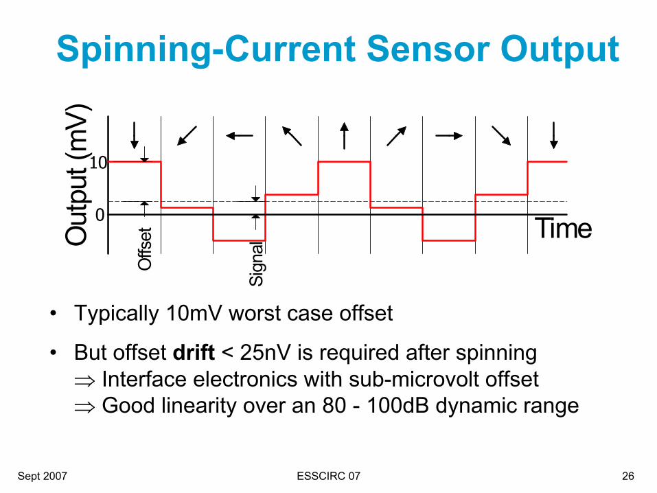
Spinning-Current Sensor Output
• Typically 10mV worst case offset
• But offset drift < 25nV is required after spinning⇒ Interface electronics with sub-microvolt offset⇒ Good linearity over an 80 - 100dB dynamic range
Time0
10
Out
put (
mV)
Offs
et
Sign
al

Sept 2007 ESSCIRC 07 27
System Architecture
Sub-microvolt offset ⇒ nested chopping
• Hall-voltages converted to currents by chopped instrumentation amplifier (fast choppers)
• Σ∆ Modulator digitizes resulting currents
• Entire front-end is again chopped (slow choppers)
• Decimation filter sums and averages Hall-voltages
DecimationCounter &
Summing Spin
SlowChopper
FastChopper
V - IInst.Amp.
Σ∆Modulator
HallSensor
FastChopper
DigitalSlow Chopper

Sept 2007 ESSCIRC 07 28
Chip Micrograph
• 0.5µm CMOS
• Area: 2.9 mm²
• Dissipates 21mW (4.2mA @ 5V)
• RS232, SPI/µwireand PWM interface
• Commercial product
Hall Sensor Inst. Amp. ADC
Timing, Control & Interfaces

Sept 2007 ESSCIRC 07 29
Sensor Offset Distribution
0
1
2
3
4
5
6
-3 -2 -1 0 1 2 3
Offset (µT) - 19 Samples
Sensor offset (3σ) < 4µT, but offset drift < 5nT per week!

Sept 2007 ESSCIRC 07 30
Heading error
-2.5-2
-1.5-1
-0.50
0.51
1.52
2.5
0 30 60 90 120150180210240270300330360
Before calibrationOffset & Gain calibrated
System Response Measurement
• Angle error < 1° after calibration and trimming!
• State-of-the-art performance!
Compass Output
-25-20-15
-10-505
10
152025
0 30 60 90 120150180210240270300330360
Rotation (degrees)
Sens
or o
utpu
ts (µ
T)
X-VectorY-Vector

Sept 2007 ESSCIRC 07 31
A Smart Temperature Sensor
• Commercial smart temperature sensorsare not very accurate (±1.0°C from –55°C to 125°C)
• By comparison: class-A Pt100 ±0.5°C
• Our goal: ±0.1°C from –55°C to 125°Cwith only a single-temperature trim

Sept 2007 ESSCIRC 07 32
Operating Principle
• substrate PNPs generate:∆VBE proportional to absolute temp. (PTAT)VBE complementary to absolute temp. (CTAT)
• ratiometric measurement:BEBE
BE
REF
TEMPVV
VVV
∆⋅α+∆⋅α
==µ

Sept 2007 ESSCIRC 07 33
Dominant Error Sources
• process spread of VBE ⇒ errors of ~3°C
• offset in ∆VBE read-out: 10µV ⇒ 0.1°C error
• mismatch in 1:p current ratioand gain α: 0.1% ⇒ 0.2°C error

Sept 2007 ESSCIRC 07 34
Single-Temperature Calibration• process spread
⇒ PTAT error in VBE
• So single-temperaturetrim is sufficient,provided all othererrors are negligible
Approach:
- reduce all errors except spread to 0.01°C level
- correct spread by trimming the bias current

Sept 2007 ESSCIRC 07 35
Block Diagram
• Bipolar core = two PNPs
• Σ∆ modulator produces bitstream bsthat is a digital representation of temperature
• bitstream is filtered and scaled by decimation filterto produce binary reading in °C

Sept 2007 ESSCIRC 07 36
Dynamic Element Matching
• Accurate 1:5 current ratio for ∆VBE⇒ rotate current sources
• Accurate 1:8 sampling capacitor ratio ⇒ rotate sampling capacitors

Sept 2007 ESSCIRC 07 37
Switched-Capacitor Front-End
• Correlated double-sampling (CDS) cancels offset and 1/f noise of 1st integrator

Sept 2007 ESSCIRC 07 38
Chopped Σ∆ Modulator
• After CDS, offset of 1st integrator is still > 10µV⇒ further offset reduction by system-level chopping

Sept 2007 ESSCIRC 07 39
Chip Micrograph
• 0.7µm CMOS
• Area: 4.5mm2
• supply voltage:2.5..5.5V
• supply current:75µA
• Bitstream output

Sept 2007 ESSCIRC 07 40
Measurement Results
24 samplesfrom 1 batch
inaccuracy (±3σ) after calibration& trimming at 30°C:
±0.1°C –55..125°C
State-of-the-art performance!

Sept 2007 ESSCIRC 07 41
New Challenges• Designing ultra-low-power autonomous and biomedical
sensors ⇒ dynamic techniques• Designing smart sensors (e.g. temp sensors)
in nanometer CMOS ⇒ time-domain signal processing• Using dynamic techniques in other analog systems
e.g. amplifiers & ADCs
• Designing smart sensors based on new types of sensors e.g. SPADs and thermal diffusivity sensors

Sept 2007 ESSCIRC 07 42
Summary• Smart sensor design is challenging!
• The following design methodology helps
– Do no harm!
– Do system design!
– Digitize early!
– Be dynamic!
• Used to realize a unique wind sensor and state-of-the-art magnetic field and temperature sensors
K.A.A. Makinwa et al, “Smart sensor design: The art of compensation and cancellation,” Proc. ESSCIRC, pp. 76 - 82, Sept 2007.

Sept 2007 ESSCIRC 07 43
• Mierij Meteo
• Xensor Integration
• NXP Semiconductors
• Dutch Technology Foundation (STW)
• Thank-You for Your Attention!
• Any questions?
Acknowledgements

Sept 2007 ESSCIRC 07 44
Background Reading1. K.A.A. Makinwa and J.H. Huijsing, “A smart wind sensor using thermal sigma-
delta modulation techniques,” Sensors and Actuators A, vol. 97-98, pp. 15 – 20,April 2002.
2. K.A.A. Makinwa and J.H. Huijsing, “A smart CMOS wind sensor,” Digest of Technical Papers ISSCC, pp. 432 – 479, Feb. 2002.
3. J. van der Meer, F.R. Riedijk, K.A.A. Makinwa and J.H. Huijsing, “A fully-integrated CMOS Hall sensor with a 4.5uT, 3σ offset spread for compass applications,”Digest of Technical Papers ISSCC, pp. 246 – 247, Feb. 2005.
4. M. A. P. Pertijs, K. A. A. Makinwa, and J. H. Huijsing, “A CMOS smart temperature sensor with a 3σ inaccuracy of ±0.1°C from −55°C to 125°C,” JSSC, vol. 40, no. 12, pp. 2805 – 2815, Dec. 2005.
5. C.P.L. van Vroonhoven and K.A.A. Makinwa, “A CMOS Temperature-to-Digital Converter with an Inaccuracy of ±0.5°C (3σ) from –55 to 125°C,” Digest of Technical Papers ISSCC, pp. 576 – 577, Feb. 2008.
6. K.A.A. Makinwa and M.F. Snoeij, “A CMOS temperature-to-frequency converter with an inaccuracy of ±0.5°C (3σ) from –40 to 105°C,” J. Solid-State Circuits, vol. 41, is. 12, pp. 2992 – 2997, Dec. 2006.
7. K.A.A. Makinwa, M.A.P. Pertijs, J.C. van der Meer and J.H. Huijsing, “Smart sensor design: The art of compensation and cancellation,” Proc. ESSCIRC, pp. 76 – 82, Sept 2007.