designing ac to dc flyback converters using - power filename: gx flyback 03242004.ppt flyback basics...
TRANSCRIPT

Filename: GX Flyback 03242004.ppt71
Designing AC to DC Flyback Convertersusing
TOPSwitch-GX

72 Filename: GX Flyback 03242004.ppt
Agenda
• Why Flyback?
• TOPSwitch-GX Flyback Design Methodology
• Application Examples– 43 W Set-top Box– 45 W LCD Monitor– 70 W Laptop Adapter– 11 W DVD Supply
• Hints & Tips

Filename: GX Flyback 03242004.ppt73
Why Flyback?

74 Filename: GX Flyback 03242004.ppt
Flyback Basics
• At switch turn-on, IP ramps up and energy is stored in the transformer
• At switch turn-off, current transitions from primary (IP) to secondary (IS)
• During switch-off, IS ramps down, as stored energy is delivered to output
• Transformer isolates, stores energy, & steps voltage down, current up
• During the switch on-time, transformer primary winding current ramps up as energy is stored in the transformer’s magnetizing inductance
• During the switch on-time, the output rectifier is reverse biased, and the secondary is an open circuit
• At switch turn-off, the transformer current transitions from the primary to thesecondary, and the drain voltage rises sharply and quickly, as the voltage across the primary winding of the transformer “flys back” ( “leakage inductance” induced)
• During the switch off-time, the transformer’s secondary current ramps down, as the stored magnetizing energy is delivered to the output, and the primary is an open circuit
• A clamp circuit (not shown) is required to limit the voltage spike on the drain node, that is induced by the transformer’s leakage inductance
• It can be seen, in this discontinuous conduction mode example, that there is “dead-time” before the beginning of the next switching cycle

75 Filename: GX Flyback 03242004.ppt
Flyback versus Forward
• Flyback– Lowest cost solution for output currents < ~ 6 Amps– Advantages:
1. Simple circuit - no output energy storage inductor required
2. Simple to implement multiple output designs– Disadvantages: higher output ripple current - higher output capacitor costs
• Forward – Lowest cost solution for output currents > ~ 6 Amps– Advantages: low output ripple - lower cost output capacitors– Disadvantages:
1. More complex circuit - output energy storage inductor required 2. Coupled output inductor required for multiple output
• Flyback is the ideal solution for applications with 0 A to 6 A output current
• Most of these applications are in the power range of 0 W to 100 W. However, applications beyond 100 W could still be suitable for flyback if output voltage is high enough to keep the output current low. (For a given output power, higher output voltage means lower output current).

Filename: GX Flyback 03242004.ppt76
TOPSwitch-GX Flyback Design Methodology
77 Filename: GX Flyback 03242004.ppt
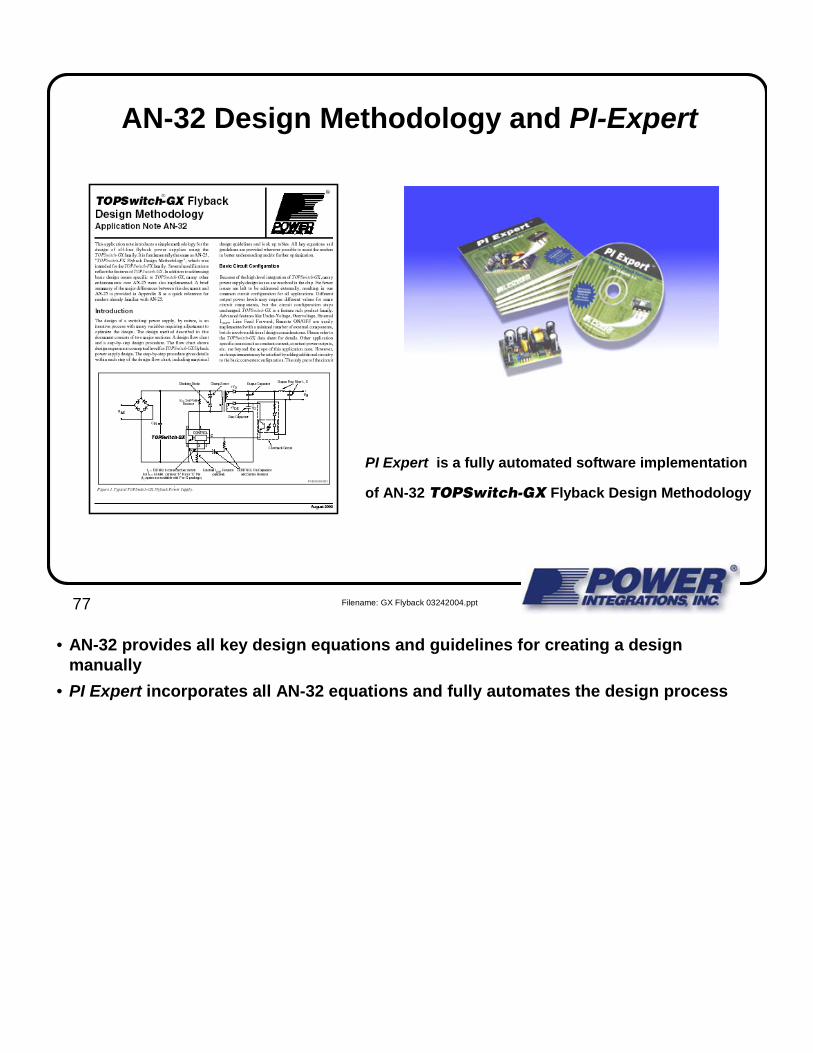
AN-32 Design Methodology and PI-Expert
PI Expert is a fully automated software implementation
of AN-32 TOPSwitch-GX Flyback Design Methodology
• AN-32 provides all key design equations and guidelines for creating a design manually
• PI Expert incorporates all AN-32 equations and fully automates the design process

78 Filename: GX Flyback 03242004.ppt
AN-32 TOPSwitch-GX Flyback Design Methodology
• Design flow chart and easy-to-follow step-by-step design procedure
• Design equations and design guidelines
• Component selection guidelines and examples
• Supports both continuous and discontinuous mode designs
• Implemented in PI Expert for fully automated design– Step 1 - 28: PI Expert handles all calculations including necessary
iterations and outputs calculated results– Step 29 - 37:Based on calculated results from PI Expert, user selects
appropriate components to complete the design
• This methodology is similar to those used for previous TOPSwitch families
• Covers basic Flyback converter design only. Other application specific issues, such as constant current or constant power outputs may be addressed by adding the appropriate circuitry to the basic converter
• Advanced TOPSwitch-GX features and functions such as UV, OV, power limiting, remote on/off etc. are not addressed within PI Expert. Please refer to the TOPSwitch-GX data sheet, for information on how to implement those features and functions

79 Filename: GX Flyback 03242004.ppt
PI Expert
• Switched mode power supply design software tool developed by Power Integrations
• Fully automated with built-in knowledge base
• Customization possible through user override (manual mode)
• Built-in data base: PI products including TOPSwitch-GX, transformer cores, bobbins and wires
• Implements steps 1 to 28 of AN-32 TOPSwitch-GX Flyback Design Methodology
• Outputs all necessary information for user to complete steps 29 - 37
• PI Expert is available free of charge to all PI customers
• Gives complete results for all calculated design parameters
• Produces information the user needs to provide to the transformer vendor

80 Filename: GX Flyback 03242004.ppt
PI Expert
Design Flow
• User enters the system requirements (step 1)
• User chooses an output feedback circuit (step 2)
• PI Expert chooses the smallest TOPSwitch-GX capable of delivering the required output power (steps 3-11)
• PI Expert designs the smallest transformer for the given TOPSwitch-GX device and output power (steps 12-26)
• PI Expert calculates secondary and bias parameters (steps 27-28)
• User selects the other components to complete the design (steps 29-37)
User
User inputs
PI Expertoutput
• Although 37 steps in length, the design flow is conceptually simple and straight forward
• The default design goal is “cost effectiveness” (to produce the lowest cost design that meets the specifications)
• The alternate design goal is “high efficiency,” which can be chose within PI Expert,or accomplished by working through the design process manually
81 Filename: GX Flyback 03242004.ppt
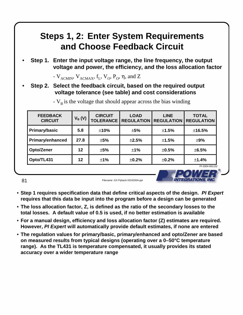
Steps 1, 2: Enter System Requirements and Choose Feedback Circuit
FEEDBACK CIRCUIT VB (V) CIRCUIT
TOLERANCE LOAD
REGULATION LINE
REGULATION TOTAL
REGULATION
Primary/basic 5.8 ±10% ±5% ±1.5% ±16.5%
Primary/enhanced 27.8 ±5% ±2.5% ±1.5% ±9%
Opto/Zener 12 ±5% ±1% ±0.5% ±6.5%
Opto/TL431 12 ±1% ±0.2% ±0.2% ±1.4% PI-3304-091102
• Step 1. Enter the input voltage range, the line frequency, the output voltage and power, the efficiency, and the loss allocation factor
- VACMIN, VACMAX, fL, VO, PO, η, and Z
• Step 2. Select the feedback circuit, based on the required output voltage tolerance (see table) and cost considerations
- VB is the voltage that should appear across the bias winding
• Step 1 requires specification data that define critical aspects of the design. PI Expertrequires that this data be input into the program before a design can be generated
• The loss allocation factor, Z, is defined as the ratio of the secondary losses to the total losses. A default value of 0.5 is used, if no better estimation is available
• For a manual design, efficiency and loss allocation factor (Z) estimates are required. However, PI Expert will automatically provide default estimates, if none are entered
• The regulation values for primary/basic, primary/enhanced and opto/Zener are based on measured results from typical designs (operating over a 0–50°C temperature range). As the TL431 is temperature compensated, it usually provides its stated accuracy over a wider temperature range

82 Filename: GX Flyback 03242004.ppt
Primary/Basic Feedback
• Lowest cost feedback configuration
Feedback Circuit
• Primary side feedback is the lowest cost solution for power supplies which do not require tight output voltage tolerance

83 Filename: GX Flyback 03242004.ppt
Primary/Enhanced Feedback
• Similar to the Primary/Basic, but with tighter output voltage tolerances
Feedback Circuit
• The 22 V Zener diode improves the accuracy of the primary side feedback by increasing the bias voltage. This effectively increases the gain of the feedback loop and reduces the dependence of the output voltage tolerance on the accuracy of the CONTROL pin voltage

84 Filename: GX Flyback 03242004.ppt
Opto/Zener Feedback
• Low cost, with good output voltage tolerance
Feedback Circuit
• The secondary Opto/Zener is a good compromise between cost and performance
• The Zener voltage tolerance and temperature coefficient must be considered in determining the overall output voltage tolerance accuracy
• Biasing the Zener diode at its specified IZT (typically 5-20 mA), usually gives the best reference accuracy. As a result, the no-load power consumption of an Opto/Zener based solution will typically be higher than will be that of an Opto/TL431 based solution
• Using a low current Zener diode will lower the no-load power consumption of the supply
85 Filename: GX Flyback 03242004.ppt
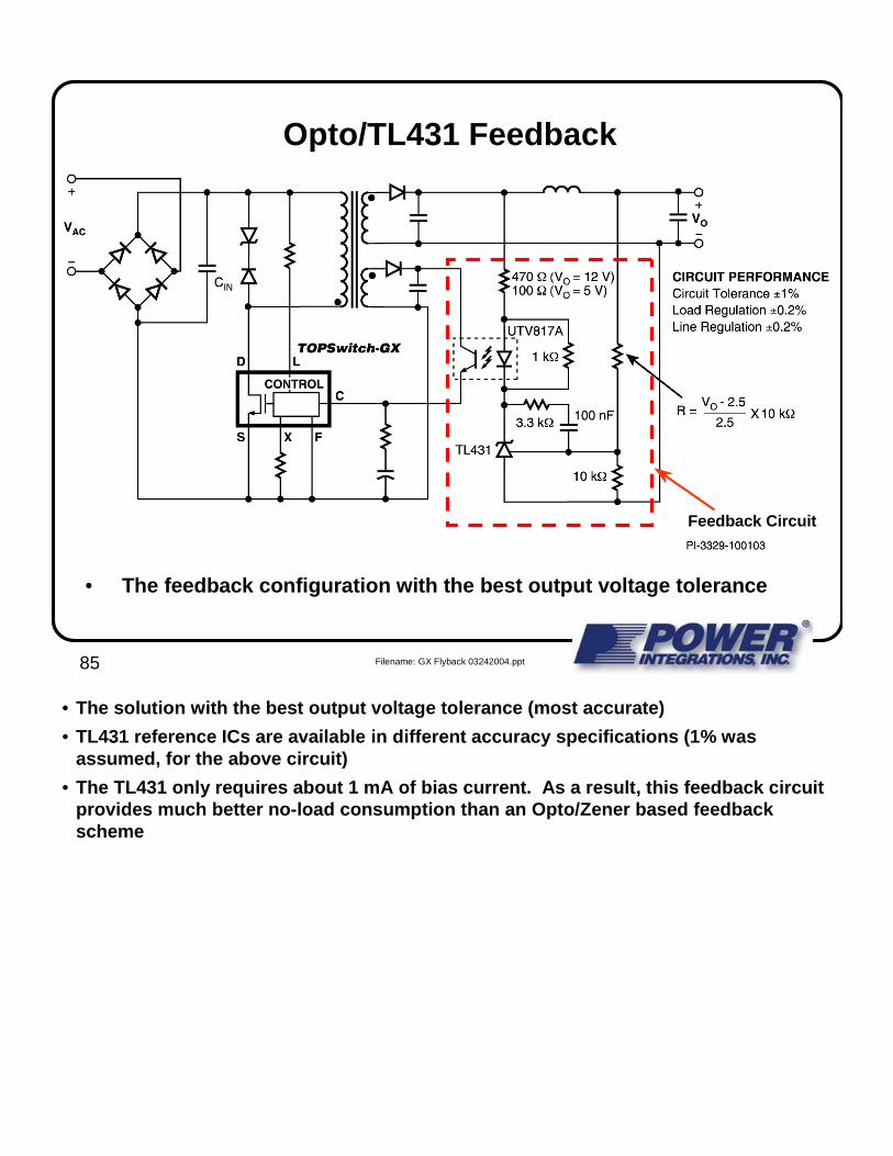
Opto/TL431 Feedback
• The feedback configuration with the best output voltage tolerance
Feedback Circuit
• The solution with the best output voltage tolerance (most accurate)
• TL431 reference ICs are available in different accuracy specifications (1% was assumed, for the above circuit)
• The TL431 only requires about 1 mA of bias current. As a result, this feedback circuit provides much better no-load consumption than an Opto/Zener based feedback scheme

86 Filename: GX Flyback 03242004.ppt
Step 3: Determine DC Input Voltages VMIN, VMAX, and Input Storage Capacitance CIN
• For universal input– CIN = 2 µF to 3 µF
per watt of output power
– VMIN = 90 V– VMAX = 375 V
• For 230 VAC input– CIN = 1 µF per watt
of output power – VMIN = 240 V– VMAX = 375 V
( )
×
−
×××
−×=IN
C
L
O
2
ACMINMIN Cη
tf2
1P2
V2V
• Input line voltage ripple varies directly with the size of the input storage capacitor CIN
• A smaller value of CIN results in a lower minimum input voltage VMIN, which reduces the power delivery capability of a given TOPSwitch-GX device, in the specified circuit
• The VMIN equation shown in the slide represents a good approximation. An exact equation has no closed form solution, and can only be solved by numerical analysis

87 Filename: GX Flyback 03242004.ppt
Step 4: Select Reflected Output Voltage (VOR) and Clamp Zener Voltage (VCLO)
• For single output– VOR = 120 V– VCLO = 180 V
• For multiple output– VOR = 100 V– VCLO = 150 V
• For maximum power– VOR = 135 V– VCLO = 200 V– The default for cost
optimization, in PI Expert
• Higher VOR increases the maximum operating duty cycle DMAX. This allows higher power delivery, at the price of reduced drain voltage margin
• Lower VOR reduces secondary peak currents and leakage inductance reflected from the secondary back to the primary, which improves cross regulation of multiple outputs
• Lower VOR will also reduce no-load power consumption, by reducing the total leakage losses (should be used in conjunction with a Zener diode clamp, for best results)
• Note: VCLO should be kept to 1.5 x VOR, to minimize the power dissipated in the clamp
• Note: the peak of the waveform shown represents Zener clamping, and includes the worst case temperature, absolute tolerance, dynamic impedance and forward recovery of the clamp diode. VCLO is the rated Zener diode avalanche voltage

88 Filename: GX Flyback 03242004.ppt
Continuous Conduction Mode (CCM)Operation (KP ≤1)
• KP is the primary current waveform parameter, and is defined at the minimum input voltage VMIN and the full specified output load
• In continuous conduction mode (CCM), KP is the ratio of the primary ripple current (IR) to the peak primary current (IP), and is also called KRP
• CCM operation:
– Does not let the transformer core magnetic flux reset to zero, before the next switching cycle
– Requires a larger transformer core, so that core saturation can be avoided
– Produces larger high-frequency (HF) noise currents, due to higher output diode reverse recovery currents (since secondary winding current is not zero when the next cycle begins)
– Results in lower peak and RMS current values (on both the primary and the secondary sides)
– Has better output voltage cross-regulation (in multi-output designs) than does DCM operation
• Deeply CCM operation occurs when IR is much less than IP (KP or KRP = 0.4 to 0.6)
– May allow the non-primary outputs of a multiple output design to meet their regulation specs without requiring linear post regulators, which lowers costs and increases efficiency

89 Filename: GX Flyback 03242004.ppt
Discontinuous Conduction Mode (DCM) Operation (KP ≥1)
• KP is the primary current waveform parameter, and is defined at the minimum input voltage VMIN and the full specified output load
• In discontinuous conduction mode (DCM), KP is the ratio of switch OFF time to the secondary (main output) diode conduction time, and is also called KDP
• DCM operation:
– Allows the magnetic flux in the transformer core to reset to zero, before the next switching cycle begins
– Allows a smaller transformer core to be used (than CCM requires), for a given amount of output power
– Eliminates output diode reverse recovery current, lowering the high frequency (EMI) noise that is generated by the normal switching process
– Produces higher peak and RMS current values (on both the primary and secondary sides)
– Has output voltage cross-regulation (in multi-output designs) that is not as tightly toleranced as would a comparable CCM design

90 Filename: GX Flyback 03242004.ppt
Step 5: Choose the Mode of Operation and Set the Current Waveform Parameter (KP)
• Continuous conduction mode (CCM) operation, KP ≤ 1– KP is the ratio of the primary ripple current to the peak primary current– For universal input, keep KP between 0.4 and 1.0. Set KP = 0.4 initially– For 230 VAC input, keep KP between 0.6 and 1.0. Set KP = 0.6 initially
• Discontinuous conduction mode (DCM) operation, KP ≥ 1– KP is the ratio of the TOPSwitch-GX MOSFET off-time to the main output
rectifier’s conduction (on) time– KP should always be kept ≥ 1. Set KP = 1.0 initially
• At borderline continuous/discontinuous conduction mode, KP = 1
• The mode of operation (CCM or DCM) determines which equation(s) are used in steps 5, 6, 7, 8 and 12
• The mode of operation also determines how the AN-29 selection curves are used in step 9
• Note: this refers to the mode of operation at VMIN (from step 3), and at the full rated output power. KP naturally increases as the input voltage increases, and/or as the power being drawn out of the supply decreases. Therefore, at light loads, most CCM designs will operate in the DCM

91 Filename: GX Flyback 03242004.ppt
Steps 6-8: Calculating the Primary Current Parameters DMAX, IP, and IRMS
• Step 6. Calculate the maximum operating duty cycle, DMAX, based onVMIN (from step 1), VOR (from step 4), and KP (from step 5)
– Use the equation appropriate for the mode of operation chosen
• Step 7. Calculate the peak primary current, IP– Use the equation appropriate for the mode of operation chosen
• Step 8. Calculate the RMS primary current, IRMS
– Use the equation appropriate for the mode of operation chosen
• AN-32 provides formulas for all parameters and PI Expert automatically uses the correct formula for the mode of operation chosen
• All three steps use different equations for CCM and DCM (see AN-32, page 10)

92 Filename: GX Flyback 03242004.ppt
AN-29 TOPSwitch-GX Selection Curves
• Efficiency vs output power curves for the TOPSwitch-GX family– Includes constant device power dissipation contours– The curves are applicable to both CCM and DCM designs
• AN-29 contains four separate sets of curves (for two input voltage ranges and two output voltages)
– Universal input, VO = 5 V, and VO = 12 V – 230 VAC input, VO = 5 V, and VO = 12 V – (for a total of 4 curves for each device in the family)
• Allows designers to– Choose the best TOPSwitch-GX device, based on the maximum output
power and the desired power supply efficiency– Estimate the TOPSwitch-GX device power dissipation, which makes
determining the required heatsink size easier

93 Filename: GX Flyback 03242004.ppt
Using AN-29 Selection Curves
TOP245 82.4%TOP244 81.5%
TOP24379%
20 W
Output Power (Watts)
• Locate the maximum specified value of output power, along the X-axis
• Draw a vertical line (see the red dotted line on the slide) up from that point
• The line may cross the curves of several TOPSwitch-GX devices
• Wherever the output power line crosses a TOPSwitch-GX curve, the predicted power supply efficiency (for a supply designed around that device) may be found by drawing a horizontal line, from that point of intersection, to the Y-axis
• A 20 W supply has three solutions: TOP243 (79%) , TOP244 (81.5%) & TOP245 (82.4%)
• Larger devices will provide better efficiency because their lower RDS(ON) reduces the conduction losses the device dissipates (at a higher cost than the smaller devices)
• The shaded area of the Selection Curves graph is not recommended for Flyback supplies, since the output currents are too high for the design to be cost effective
• For CCM designs, use the selection curves “as is”
• For DCM designs, the output power must be derated by 33%. Example: A 20 W DCM design must use the 30 W point on the selection curve [30 W x 0.66 ≈ 20 W]

94 Filename: GX Flyback 03242004.ppt
Steps 9-11: TOPSwitch-GX Selection and Validation with Current Limit Reduction
• Step 9. Select a TOPSwitch-GX device using AN-29 selection curves– Choose the best curve set, within AN-29, based on the VIN range and VO
– Select a TOPSwitch-GX device, based on output power PO, and efficiency η– For a CCM design, use the selection curves “as is”– For a DCM design, derate the output power by 33% before using the curves
• Step 10. Program ILIMIT by setting current limit reduction parameter, KI
– KI is determined by the resistor value that connects the X (or M) pin to the SOURCE pin of the device (see the TOPSwitch-GX data sheet, figures 54 & 55)
• Step 11. Validate the TOPSwitch-GX device choice: verify that IP does not exceed the product of “the derating factor” and ILIMIT(min)
• Step 9. Examples:
– For a high voltage only VIN (230 VAC, ± 15%) 24 VDC out, 50 W DCM design that needs to meet an efficiency target of 80%, the 75 W output point on curve set (figure) 3 intersects the curves for the TOP245, the TOP246 and the TOP247
– For a Universal VIN (85–265 VAC) 3.3 VDC out, 20 W CCM design that needs to meet an efficiency target of 70%, the 20 W output point on curve set (figure) 2 intersects the curves for the TOP244, and the TOP245
• Step 10. Benefits of ILIMIT reduction:
– Reduces the overload power that can be drawn from the supply’s output
– Applications requiring very high efficiency may benefit from the lower RDS(ON) of a larger TOPSwitch-GX device, operated with an externally reduced current limit
– Once it has been determined how much the current limit (ILIMIT) is to be reduced, TOPSwitch-GX datasheet figures 54 or 55 should be used to determine the value of the resistor needed to externally program the current limit
– The resistor value should not be outside of the range of 7kΩ to 45 kΩ, and the current that it draws from the X (or M) pin should not be outside the range of 25 µA to 165 µA

95 Filename: GX Flyback 03242004.ppt
Choose Heatsink Based on Device Dissipation
TOP2430.6 W
TOP2421.1 W
• TOPSwitch-GX selection curves provide estimated device dissipation
• Example: Universal input, 10 W, 5 V output
– TOP242 dissipates 1.1 W– TOP243 dissipates 0.6 W
• Choose heatsink with thermal impedance (θCA) to maintain junction temperature (TJ) below 100 °C
• Definitions of thermal terms:
• TJ is the junction temperature of the TOPSwitch-GX device, TA_INT is the internal ambient temperature of the power supply enclosure, θJA is the thermal impedance from the device junction to the external ambient temperature, θJC is the thermal impedance from the device junction to the device case temperature, θCA is the thermal impedance from the device case to the ambient temperature, and PD is the internal TOPSwitch-GX device power dissipation
• Use the quick selection curves, located within AN-29, to estimate the TOPSwitch-GXdevice power dissipation
• Use the “dotted” constant power contour lines to compare the dissipation and relative efficiency of different TOPSwitch-GX devices
• Note: Thermal calculations are not presently included in PI Expert

96 Filename: GX Flyback 03242004.ppt
Steps 12-26: Transformer Design
• Step 12. Calculate the inductance of the primary transformer winding– Use the equation appropriate for the mode of operation (CCM or DCM) chosen
• Step 13. Choose a core and bobbin
• Steps 14-16. Set the number of primary winding layers, and the number of secondary turns, then calculate the number of primary and bias winding turns, and the primary wire size parameters (OD, DIA, & AWG)
• Steps 17-22. Calculate and check maximum flux density BM, current capacity CMA, and gap length Lg. Iterate if necessary
– Check that BM < 3000 gauss (0.3 T), Lg ≥ 0.1 mm, and that 500 ≥ CMA ≥ 200
• Step 23. Calculate and check peak flux density BP– Check that BP < 4200 gauss (0.42 T)– BP is the maximum flux density (seen during startup and output overload)
• Steps 24-26. Calculate secondary peak current ISP, RMS current ISRMS, wire gauge (or size) and current capacity CMAS
• Step 12: CCM and DCM use different equations (see AN-32, page 10)
• Steps 13-22 are usually a highly iterative process. However, PI Expert performs all of the iterations automatically!
• Step 23: Peak flux density BP occurs during start up and overload conditions (BM , the maximum flux density, occurs during normal operation)
• Note: 500 ≥ CMA ≥ 200 (circular mils/A) is equivalent to 4 ≤ S ≤ 10 A/mm2

97 Filename: GX Flyback 03242004.ppt
Steps 27, 28: Calculate the Remaining Secondary Side Parameters
• Step 27. Determine the output capacitor ripple current IRIPPLE
– This is necessary for selecting the output capacitor
• Step 28. Determine the maximum peak inverse voltages (PIVS, PIVB) for the secondary and the bias windings
– This is necessary for selecting the output and bias rectifier diodes
• After step 28, PI Expert is finished with its calculations and produces an Excel spreadsheet styled text file that contains all of the results. The designer then must complete steps 29-37, based on the results produced from the calculations, just as he or she would if they were creating the design manually

98 Filename: GX Flyback 03242004.ppt
Step 29: Select Clamp Components
• Step 29. Select the Zener clamp diode and the blocking diode
• An RCD clamp may be used with TOPSwitch-GX, if power limiting is used via the X (or M) pin’s external current limiting function
– Power limiting will reduce RCD clamp dissipation and allow a higher VOR
– See the “Flyback Design Hints & Tips” section, for the RCD clamp design considerations that must be taken into account before using an RCD clamp
PS OUTPUT VORBLOCKING
DIODECLAMPZENER
Multiple Output 100 VBYV26CMUR160UF4005
P6KE150
Single Output 120 V135 V
BYV26CMUR160UF4005
P6KE180P6KE200
PI-3386-052003
• An RCD clamp cost less, but is less efficient than a Zener clamp, at light loads
• The RCD clamp voltage is highly affected by the output load. It is also sensitive to the tolerance variations of the clamp component values
• When using an RCD clamp, make sure that the drain voltage is clamped to a safe level, under the worst case conditions (particularly output overload, and the extremes of clamp component value variations). Always check the final design against the quick design checklist criteria (see slide 102)

99 Filename: GX Flyback 03242004.ppt
Steps 30-32: Select Output Components
• Step 30. Select the output rectifier, based on PIVS (from step 28)– VR ≥ 1.25 X PIVS, where VR is the diode rated reverse voltage– ID ≥ 3 X IO, where ID is the diode rated DC current
• Step 31. Select the output capacitor based on the calculated ripple current IRIPPLE (from step 27)
– The capacitor’s ripple current spec at 105 °C, 100 kHz must be ≥ than IRIPPLE
– A low ESR, electrolytic capacitor should be used
• Step 32. Select the output post LC filter values (if necessary)– Inductor value: 2.2 to 4.7 µH. A ferrite bead can be used for low current
outputs, and standard off-the-shelf inductors for higher current outputs– The Inductor must be rated for the highest output current to avoid saturation– Capacitor value: 100 to 330 µF, electrolytic of appropriate voltage rating
• Step 31: For electrolytic capacitors with breakdown voltages below 35 V, the case size determines ESR. When choosing between capacitors in the the same case size, choose a higher voltage and a lower capacitance, for a wider bandwidth
• Output switching ripple voltage = IRIPPLE x ESR of the output capacitor
• Avoid saturating the output post filter inductor, at full load or overload currents
• Note: ID ≥ 3 x IO is a general “rule of thumb” for limiting rectifier diode dissipation
• Note: for CCM designs, the diode should be an ultra-fast (trr<50 ns) recovery type. For DCM designs, fast recovery diodes may be used (trr < 250 ns)

100 Filename: GX Flyback 03242004.ppt
Steps 33-37: Select Other Components
• Step 33. Select bias rectifier based on PIVB (from step 28)– VR ≥ 1.25 X PIVB, where VR is the diode rated reverse voltage
• Step 34. Bias capacitor: 1 µF, 50 V, electrolytic
• Step 35. CONTROL pin capacitor and series resistor – 47 µF, 10 V, electrolytic (low-ESR not required) & 6.8 ohm
• Step 36. Feedback circuit components – See reference feedback circuits (in step 2) for typical values
• Step 37. Select input bridge rectifier– VR ≥ 1.75 X VACMAX, where VACMAX is from step 1– ID ≥ 2 X IAVG, where ID is the bridge diode rated RMS current– Note: IAVG = PO/(η X VACMIN X PF)
• Upon completion, a design must be built and checked against Quick Design Check List

101 Filename: GX Flyback 03242004.ppt
EMI Filter Design• Refer to application examples for EMI filter designs
• Follow the TOPSwitch-GX data sheet PC board layout guidelines
• For >10 W, a single stage EMI filter (CM inductor, X cap. & Y cap.) – See Design Ideas for example filter circuits
• The Y-capacitor should be connected to the high voltage DC + rail, not to the high voltage DC – (primary return) rail
– Routes common mode surge currents away from the TOPSwitch-GXdevice, and keeps the noise current path length and impedance minimized
• For further improvements, try the following in this order:– Optimize the transformer construction – Improve the PC-board layout– Use a different (higher inductance value) common mode (CM) inductor– Increase the size (capacitance) of the X-capacitor
• For ≤10 W applications:– Supplies without a CM inductor are feasible, with a bulk-cap “π ” filter– Supplies without a Y cap are feasible, with transformer shield windings
• EMI filter design is empirical in nature, and is not covered in AN-32

102 Filename: GX Flyback 03242004.ppt
Quick Design Checklist
• Maximum drain-node voltage– Test condition: maximum input voltage, and maximum output overload– Verify that the peak drain voltage remains under 675 V
• Maximum drain current– Test condition: VMIN, output load and ambient temperature are both maximum– Verify that the transformer core doesn’t saturate, at start-up or when overloaded– Verify that the initial current spike is within the leading edge blanking time, and
that the drain current is within the operating envelope (data sheet, figure 52)
• Thermal– Verify that the temperature of each key component is under its maximum limit,
at VMIN, the maximum output load, and the maximum ambient temperature– The recommended maximum TOPSwitch-GX SOURCE pin (or package tab)
temperature is 100 °C, with full ILIMIT, and 110 °C with a reduced ILIMIT
– See the manufacturers specifications for key component temperature limits
• All designs should be verified as being in compliance with the criteria in this checklist, before being released into mass production
• Maximum overload output power occurs when the output of the power supply is loaded to the point just before the TOPSwitch-GX enters its auto-restart mode
• See Figure 52, of the TOPSwitch-GX data sheet, for a normalized graphical depiction of the drain current operating envelope
• Key components are: input diodes, the TOPSwitch-GX device, the drain-node clamp components, the power transformer, the output diodes and the output capacitors
• Leave enough thermal margin for the normal device-to-device variation of the TOPSwitch-GX RDS(ON) parameter

103 Filename: GX Flyback 03242004.ppt
Design Support
• AN-29 TOPSwitch-GX Flyback Quick Selection Curves
• AN-32 TOPSwitch-GX Flyback Design Methodology
• PI Expert - Full optimization for Flyback supplies
• Many Design Ideas (DI-16, DI-21, DI-22, DI-41, DI-55 etc.)
• Also, Design Accelerator Kits for hardware evaluation (DAK-18, DAK-32, DAK-33 and DAK-34 )
• AN = Application Note, DI = Design Idea, and DAK = Design Accelerator Kit

104 Filename: GX Flyback 03242004.ppt
Flyback Application Examples
DI: Design Idea
• 43 W (57 W pk) Set-top box Supply (DI-16/DI-41)– 3.3 V, 5 V, 12 V, 18 V and 33 V
• 45 W LCD Monitor Supply (DI-21)– 12 V/3.75 A
• 70 W Laptop Adapter Supply (DI-22)– 19 V/3.66 A
• 11 W (17 W pk) DVD Supply with 100 mW standby (DI-39)– 3.3 V, 5 V, 12 V and -12 V– uses current-mode control and reduced switching frequency,
for low standby power consumption
• All design ideas (DI) may be found on the PI web site, at www.powerint.com/appcircuits.htm
105 Filename: GX Flyback 03242004.ppt
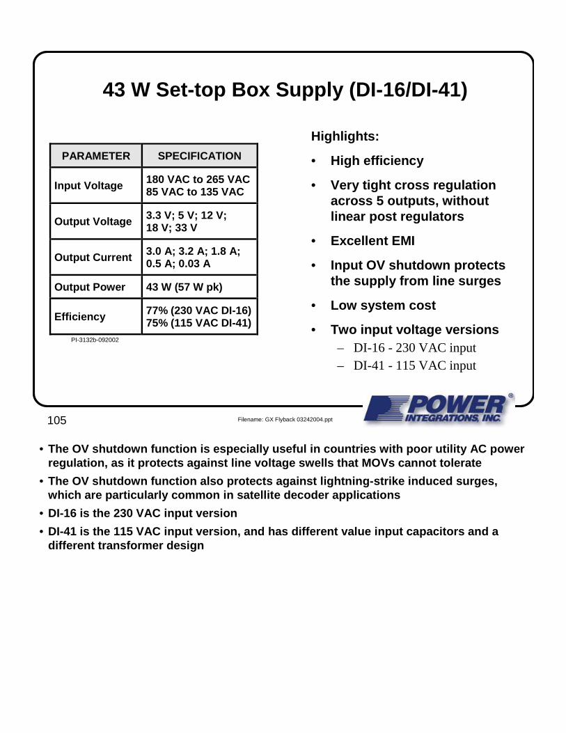
43 W Set-top Box Supply (DI-16/DI-41)
Highlights:
• High efficiency
• Very tight cross regulation across 5 outputs, without linear post regulators
• Excellent EMI
• Input OV shutdown protects the supply from line surges
• Low system cost
• Two input voltage versions– DI-16 - 230 VAC input– DI-41 - 115 VAC input
PARAMETER SPECIFICATION
Input Voltage 180 VAC to 265 VAC 85 VAC to 135 VAC
Output Voltage 3.3 V; 5 V; 12 V; 18 V; 33 V
Output Current 3.0 A; 3.2 A; 1.8 A; 0.5 A; 0.03 A
Output Power 43 W (57 W pk)
Efficiency 77% (230 VAC DI-16) 75% (115 VAC DI-41)
PI-3132b-092002
• The OV shutdown function is especially useful in countries with poor utility AC power regulation, as it protects against line voltage swells that MOVs cannot tolerate
• The OV shutdown function also protects against lightning-strike induced surges, which are particularly common in satellite decoder applications
• DI-16 is the 230 VAC input version
• DI-41 is the 115 VAC input version, and has different value input capacitors and a different transformer design

106 Filename: GX Flyback 03242004.ppt
43 W Set-top Box Supply (DI-16/230 VAC)
Zener/Capacitor Clamp, for high efficiency
DC stacking
Current limit reduction and voltage mode enable an optimum design for CCM operation
OV shutdown provides surge protection
Shared 5 V and3.3 V
sensing, for better regulation
VOR of 100 V improves cross regulation
• The line sense resistor (R1) forces the power supply to shutdown during overvoltage conditions, increasing the surge withstand rating to 700 VDC (495 VAC). The input capacitors must also be rated to withstand the surge voltage
• In combination with an MOV, the OV shutdown function allows a 4 kV surge protection rating to be achieved
• This combination improves the ruggedness of the supply, which can be extremely important for set-top boxes and other applications that are exposed to lightning-induced surges
• DC-stacking provides tight cross regulation of the higher voltage outputs
• The bias winding return is connected directly to the bulk capacitor. This routes common mode surge currents away from the TOPSwitch-GX device
• The Zener clamp diode (VR1) conducts (clamps) only during load transients and during the initial power supply start-up. This increases the full load efficiency, since the RCD clamp was designed only for the nominal full load (43 W) condition
• Note: the VOR in this design was held to 100 V, for better cross regulation

107 Filename: GX Flyback 03242004.ppt
Efficiency versus Input Voltage (DI-16)
TOPSwitch-GX circuits can be easily designed for deep CCM operation, reducing the peak currents and giving very high efficiency
• CCM = continuous conduction mode (see slide 88)

108 Filename: GX Flyback 03242004.ppt
Cross-regulation Performance
VOUT
(V) MIN TYP MAXRIPPLE
VOLTAGE atFULL LOAD
MIN/MAXLOAD FOR
EACH OUTPUT%
3.3 3.14 3.3 3.46 33 mV 1.0 to 3.0 A ±5
5 4.75 5.0 5.25 50 mV 1.0 to 3.2 A ±5
12 11.16 12.0 12.84 120 mV 0.3 to 0.6 A(1.8A pk) ±7
18 16.74 18.1 19.26 180 mV 0.5 A ±10
33 29.7 33.0 36.3 200 mV 0.01 to 0.03 A ±10 PI-3133-050903
Deep CCM operation provides excellent cross regulation without the need for linear post regulators
• A major cause of poor cross regulation is the voltage drop that occurs across inter-winding leakage inductance when peak currents are high
• Deep CCM operation minimizes the peak currents, and thereby tends to improve the cross-regulation of those outputs that are not directly sensed in the feedback control loop and depend upon their turns ratio for regulation
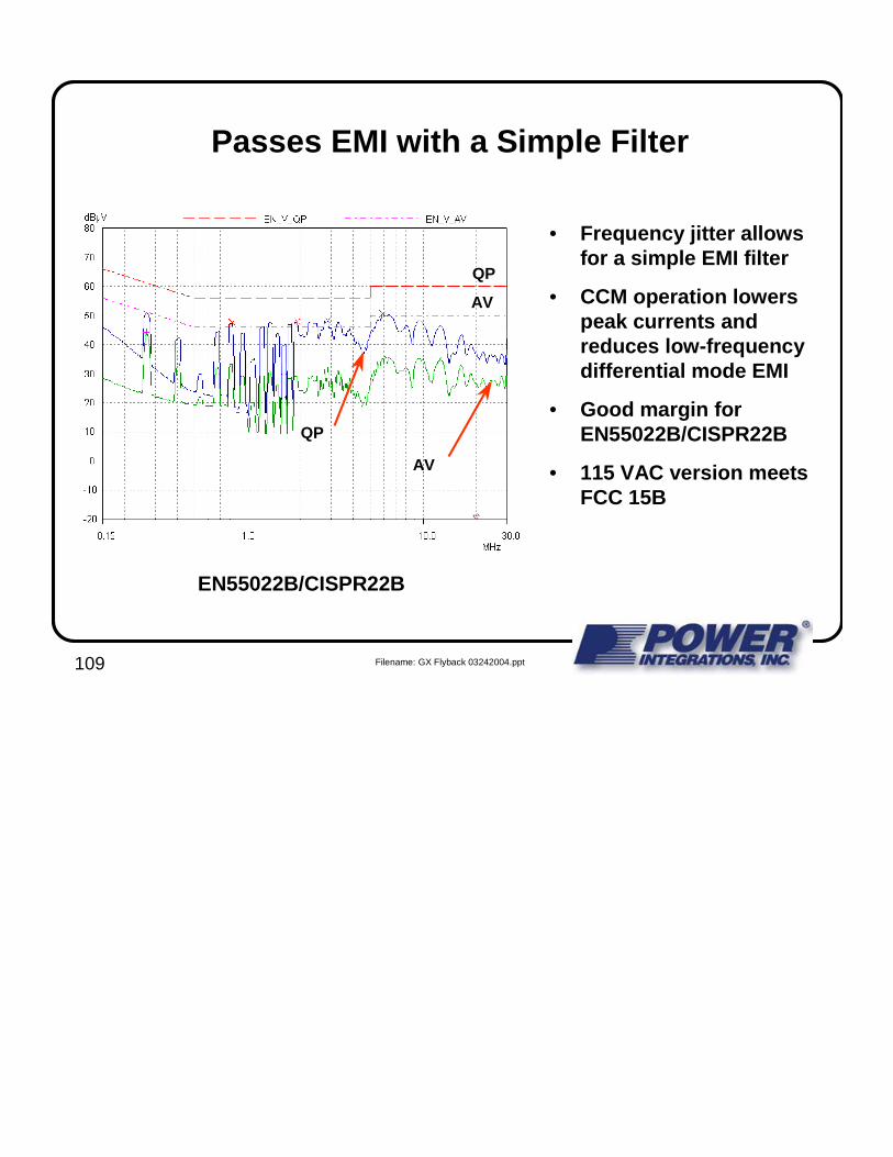
109 Filename: GX Flyback 03242004.ppt
EN55022B/CISPR22B
QP
AV
QP
AV
Passes EMI with a Simple Filter
• Frequency jitter allows for a simple EMI filter
• CCM operation lowers peak currents and reduces low-frequency differential mode EMI
• Good margin for EN55022B/CISPR22B
• 115 VAC version meets FCC 15B

110 Filename: GX Flyback 03242004.ppt
PARAMETER SPECIFICATION
Input Voltage 90 VAC to 265 VAC
Output Voltage 12 ±5%
Output Current 3.75 A
Output Power 45 W
Efficiency 82%
No load (230 VAC) (115 VAC)
380 mW 250 mW
Surge 4 kV PI-3134b-092002
45 W LCD Monitor Specification (DI-21)
• High efficiency
• Very low component count
• Low system cost
• Low no-load/standby power
• Extremely low EMI– meets FCC Part 15B,
with > 10 dB margin– meets EN55022B/CISPR22B
• Overload power is limited
• 90 VAC to 265 VAC input voltage
• The original figures for no-load power consumption were based on an older design. The figures in parentheses represent the performance of an improved design. Improvements included a transformer redesign, to lower the inter-winding capacitance of the primary winding, and the replacement of R11 with a diode
380 (250) mW250 (160) mW

111 Filename: GX Flyback 03242004.ppt
45 W LCD Monitor Schematic (DI-21)
Frequency jitteringand deep CCMoperation simplifyEMI filter
Wide DCMAXreduces input cap.
Zener/Capacitor Clamp reduces no-load consumption
132 kHz operation and ILIMIT reduction keep transformer smallILIMIT reduction with
line voltage limits overload power
EMI Passes FCC Bwith a grounded secondary return
Input line UV & OV protection R7 damps ringing on
the shield winding
VOR of 100 V maximizes efficiency
• Note: most LCD monitors have 3-wire input connectors [Line, Neutral and Ground]. The output return is usually grounded. The Ferrite bead (L5) is important for passing EMI with the secondary return hard-wired to the input safety ground
• C3 reduces the dissipation in the Zener clamp diode, VR1. Resistor R18 damps out the high frequency ringing that occurs between the transformer leakage inductance and C3, improving EMI
• The VOR of this design was held to 100 V to maximize the efficiency of the supply

112 Filename: GX Flyback 03242004.ppt
High Efficiency and Low No-load Consumption
Efficiency vs Output Power No-load Input Power vsInput Voltage
• CCM operation reduces the RMS currents, improving efficiency
• The TOPSwitch-GX light-load frequency reduction keeps the no-load consumption low, maintaining high efficiency even during light loading
• With the redesigns mentioned on slide 110, no-load power was reduced to 250 mW (for 230 VAC operation) and 160 mW (for 115 VAC operation)

113 Filename: GX Flyback 03242004.ppt
EMI Performance
AV
QP
FCC B EN55022B/CISPR22B
• > 10 dB margin FCC Part B
• > 15 dB margin EN55022B/CISPR22B
QP
AVQP

114 Filename: GX Flyback 03242004.ppt
70 W Laptop Adapter Specification (DI-22)
• Full power (70 W) in an enclosure that is at 40 °C external ambient
• High efficiency – 84% at 115 VAC– 89% at 230 VAC
• High power density 7 W/in3
• Overload power limit – 4 A at 85 VAC– 5 A at 265 VAC
PARAMETER SPECIFICATION
Input Voltage 85 – 265 VAC
Output Voltage 19.2 V
Output Current 3.66 A
Output Power 70 W
Efficiency 84%
No load (230 VAC) (115 VAC)
520 mW 370 mW
PI-3135-091602
• Efficiency was measured with the power supply inside a laptop adapter enclosure, and an external ambient temperature ofS 40 °C

115 Filename: GX Flyback 03242004.ppt
Wide DCMAX allowsa small input cap(≅ 2 µF/W)
Zener/Capacitor Clampimproves no-load consumption Output Diodes
- twin windings with twin diodesfor thermal sharing
External ILIMIT:- limits overload power- allows CCM operation
with a small transformer
70 W Laptop Adapter Schematic (DI-22)
132 kHz operation keeps the transformer small
VOR of 120 V optimizes power delivery and efficiency
• The VOR of this design was set at 120 V, to optimize power delivery and efficiency

116 Filename: GX Flyback 03242004.ppt
High Efficiency and Low No-load Consumption
Efficiency vs Output Power
115 VAC 230 VAC
No-load Input Power vsInput Voltage
AC Input
117 Filename: GX Flyback 03242004.ppt
Ripple and Transient Response
VOUT_AC
IOUT
600 mVpk-pk
Output Ripple (Full Load) Transient Response
85 VAC at 3.6 A43 mVp-p for a 19 V output
3.66 A - 0.5 A - 3.66 ANote: Measured with 6 ft. output cable
5 ms/div 5 ms/div2 A/div
43 mV
200 mV/div
+
− −
+

118 Filename: GX Flyback 03242004.ppt
EMI Performance
QP
AV
Conducted EMI at 70 W (230 VAC) with the Artificial Hand connected
EN55022B/CISPR22B
AV
QP
• The Artificial Hand is connected to the output of a power supply, and capacitivelycouples it to ground. This typically produces the worst case conducted EMI test results

119 Filename: GX Flyback 03242004.ppt
11 W DVD Supply with 100 mW Standby (DI-39)
• Current mode with frequency reduction, for extremely low no-load/standby power consumption
• High Efficiency
• Very low component count
• Low system cost
• Extremely Low EMI– No common mode choke – Meets FCC Part 15B
with >10 dB margin– Meets EN55022B/CISPR 22B
PARAMETER SPECIFICATION
Input Voltage 85 VAC to 265 VAC
Output Voltage 3.3 V; 5 V; 12 V; -12 V
Output Current 0.7 A ; 1.6 A; 0.4 A; 0.1 A
Output Power 11 W (17 W pk)
No Load Consumption
66 mW (115 VAC)
74 mW (230 VAC)
Efficiency 75%
PI-3354-091202
• The power supply featured in DI-39 uses current mode with frequency reduction, which is described in the “TOPSwitch-GX Basic Operation” section (see slide 45)
• This mode of operation has all the characteristics of current mode control, and excellent no-load/standby power consumption

120 Filename: GX Flyback 03242004.ppt
11 W DVD Supply with 100 mW Standby (DI-39)Zener/Capacitor Clamp improves no-load consumption
Current-mode and frequency reduction operation realize
<100 mW of no-load consumption
Frequency jittering & deep CCMoperation allow low cost π filter for EMI
VOR of 120 V optimizes power delivery and cross regulation
• Current-mode operation with frequency reduction is described in the TOPSwitch-GXBasic operation portion of these seminars (see slides 44 through 46)
• The VOR of this design was set at 120 V to optimize power delivery while maintaining good cross regulation

121 Filename: GX Flyback 03242004.ppt
Flyback Design Hints and Tips

122 Filename: GX Flyback 03242004.ppt
Output Capacitor and Post LC Filter
Size for ripple, not control loop
Set the LC resonant frequency lower than 10% of the switching frequency
• R11 is used to provide ~ 1 mA of bias current to the TL431 (U3)
• R10 programs the high frequency loop gain
• R14 and C12 provide frequency compensation for the TL431 (they reduce its gain in the mid to high frequencies range)
• R12 and R13 determine the DC regulation set point for the output voltage
• R1 and C2 provide frequency compensation for the TOPSwitch-GX device
• C1 does not affect the feedback loop, and solely provides local decoupling for the TOPSwitch-GX device

123 Filename: GX Flyback 03242004.ppt
Flyback RCD Clamp Design Considerations
• An RCD clamp is not a ‘hard’ clamp– Unlike a Zener clamp, the voltage across an RCD clamp changes significantly
with component value tolerances and operating (particularly loading) conditions
• To minimize RCD clamp dissipation, minimize the peak primary currents– DCM designs: program the current limit to a level needed for full load– CCM designs: program the current limit to a level needed for full load, at the
lowest line voltage. Use current limit reduction withincreasing line voltage to lower the high line current limit
• Ensure that the drain-node voltage stays below the BVDSS of the TOPSwitch-GX, under the worst case conditions (high line, maximum overload, and the worst case RC component value tolerances)
– See the Quick Design Checklist for verification recommendations
• When designing an RCD clamp, the drain-node voltage must be kept below the BVDSS rating of the TOPSwitch-GX device, under all worst-case operating conditions, including component value variations
• Reducing the TOPSwitch-GX current limit as the line voltage increases reduces the need to over size the RCD clamp components (for overload at high line). This also reduces clamp component dissipation at low line, which improves efficiency
• DCM designs operate at a fixed peak current, independent of line voltage. Therefore, programming the primary current limit to just above that needed for full load optimizes the RCD clamp dissipation, and keeps efficiency as high as possible (for an RCD clamp)

124 Filename: GX Flyback 03242004.ppt
Power Limiting Optimizes RCD Clamp Design
VDRAIN peak with power limiting265 VAC at maximum overload
656 V peak - Adequate margin to 700 V
VDRAIN peak without power limiting260 VAC at maximum overload
VDRAIN
200 V/div
IDRAIN
0.2 A/div
712 V peak - Unacceptable drain voltage
656 V 712 V712 V
• Power limiting reduces the TOPSwitch-GX current limit as line voltage increases
• This reduces the size of the RCD clamp components needed to keep VDRAIN < BVDSS, during overloads at high (input) line
• This also optimizes the RCD clamp for low line conditions
• The lowered clamp dissipation increases the efficiency of the power supply
• Both waveforms (shown in the slide above) were measured on the same supply, with and without the power limiting function activated. To keep an adequate drain voltage margin without using the power limiting function, the size (and the value) of the RCD clamp components would have to be increased, and the amount of power that they would dissipate would also be greater

125 Filename: GX Flyback 03242004.ppt
Efficiency: RCD vs Zener clamping
• A properly designed RCD clamp can provide the same or better efficiency than a Zener clamp circuit can, but only at full load
• The Zener clamp minimizes the clamp losses across the load range– With RCD clamping, efficiency falls significantly as the load is reduced
• A Zener clamp will give the lowest no-load power consumption– RCD clamp losses will cause a higher no-load power consumption– Also, a power supply with an RCD clamp will typically not enter the
normal Eco-Smart frequency reduction mode, due to the clamp losses(another factor that increases RCD no-load power consumption)

126 Filename: GX Flyback 03242004.ppt
Typical RCD Clamp Component Values
• Clamp Capacitor– Values in the range of 1 nF to 47 nF– The voltage across the capacitor rises as the leakage inductance energy charges it – A higher value is needed for larger TOPSwitch-GX devices and for transformers
with higher values of primary leakage inductance– Ensure that the capacitor used is specified for high rates of di/dt
• Polyester and some other metalized film (capacitor) types are good choices
• Clamp Resistor– Values in the range of 10 kΩ to 100 kΩ, and wattage ratings of 1 W to 3 W– The resistor dissipates the energy stored by the capacitor and ensures that it is
adequately discharged before the switch turns off again (the next switching cycle)– The larger the TOPSwitch-GX device being used, or the higher the transformer’s
primary leakage inductance is, the smaller the resistor value should be

127 Filename: GX Flyback 03242004.ppt
Typical RCD Clamp Component Values, cont.
• Clamp (blocking) Diode– Use a fast or an ultra-fast (trr <250 ns) diode, especially for high power designs– A slow PN diode (e.g. 1N4007GP) can be used below ~15 W
• Glass-passivated diodes are recommended to ensure a specified recovery time (trr ≈ 2 µs), which can help recover some of the energy stored in the clamp capacitor
• A 10 Ω to 100 Ω resistor, in series with the slower clamp diode, limits drain ringing, and can prevent the drain from ringing below the source
• Do not neglect component value tolerances– Capacitance tolerances of ±20% are common– If using a ceramic capacitor, consider the dielectric type (X7R, NPO, Z5U)
• Some have poor voltage and/or temperature coefficients

128 Filename: GX Flyback 03242004.ppt
TOPSwitch-GX PCB Layout Considerations
• TOPSwitch-GX is a precision, high frequency, high current power IC
• PCB layout is critical to achieving optimum performance
• The suggested guidelines should be followed as closely as possible

129 Filename: GX Flyback 03242004.ppt
Primary-Side Layout Suggestions TO-220
Keep connections to the X and L pins away from the switching nodes
- Prevents noise pick-up - The source trace shields the X and L
pin traces from the drain trace
Return Bias winding directly to bulk cap
- Routes common mode surge currents away from TOPSwitch-GX
Source is electrically connected to tab
- Do not electrically connect the heatsinkto any PCB circuit traces
Keep drain and clamp loops short -Improves EMI
Return all X, L and CONTROL pin components to the source by a separate trace that does not carry switching currents

130 Filename: GX Flyback 03242004.ppt
Primary Side Layout Suggestions - DIP8/SMD8
Maximize PC Boardheatsink area
- Connected to Source for low EMI
Keep drain and clamp loops short -Improves EMI
Return Bias winding directly to bulk cap
- Routes common mode surge currents away from TOPSwitch-GX
Keep connections to M pin away from switching nodes
- Prevents noise pick-up- The source trace shields the M pin
trace from the drain trace
Return all M and CONTROL pin components to the source by a separate trace that does not carry switching currents
• DIP8 and SMD8 packages combine the X and L pin functions into the M pin

131 Filename: GX Flyback 03242004.ppt
Primary Side Layout Suggestions - D2PAKKeep drain and clamp loops short -Improves EMI
Return the bias winding directly to the bulk cap
- Do not share the trace with the TOPSwitch-GX
- This routes commonmode surge currentsaway from the TOPSwitch-GX
Return all X, L and CONTROL pin components to the source by a separate trace that does not carry switching currents
Connect PCB copper to the device tab
- Unlike other D2PAK devices, the TOPSwitch-GX tab is NOT a high current pin
- High currents should go through the SOURCE pin
Keep connections to the X and L pins away from the switching nodes
- Prevents noise pick-up - The source trace shields the X and L
pin traces from the drain trace

132 Filename: GX Flyback 03242004.ppt
Secondary–Side Layout Suggestions
Return Y capacitor to the positive DC rail- Routes common mode surge currents away from the TOPSwitch-GX- Minimizes return current loop area
Notched trace- Steers high frequency
current to capacitor pin- Reduces heat transfer
from diode to capacitor
Keep diode to output capacitor loop short
- Improves EMI & reduces clamp loss

133 Filename: GX Flyback 03242004.ppt
Secondary–Side Layout Suggestions for Multiple Output Capacitor Designs
Notch in trace- Steers high
frequency current through capacitor
- Reduces transfer of heat from diodeto capacitor
Equal lengths of parallel capacitor traces helps them share the ripple current more equally
Return Y capacitor to positive DC rail-Routes common mode surge currents away from TOPSwitch-GX-Minimizes return current loop area
This copper area is the output diode heatsink
Keep the output diode capacitor loop short

134 Filename: GX Flyback 03242004.ppt
Input capacitance value:230 VAC only: 1 µF/Watt, 230/115 VAC with a voltage doubler stage: 1-2 µF/Watt, Universal or 100 VAC only: ≥3µF/Watt
Design for Efficiency/Low No-Load Consumption
Zener may be replaced with a TL431, to lower the no-load consumption (see Opto/TL431 feedback circuit)
66 kHz switching selected for lower switching losses
Zener clamp- Minimizes clamp losses
across the load range
Keep VOR ≤ 100 V- Lower VOR lowers transformer turns ratio- Reduces reflected leakage inductance- Reduces clamp dissipation
Designed for deep CCM operation (recommended KRP = 0.4 to 0.6)- Reduced current limit allows CCM without requiring a larger core- Reduces the RMS drain current- Lowers conduction losses
• The input capacitor values shown were chosen to minimize the input ripple, which allows the efficiency to be the highest
• 66 kHz operation may also be used to improve efficiency, and to reduce no-load power consumption

135 Filename: GX Flyback 03242004.ppt
Design for Low Cost
Input capacitance value:230 VAC only: 1 µF/Watt, 230/115 VAC with a voltage doubler stage: 1-2 µF/Watt, Universal or 115 VAC only: ≥3µF/Watt
RCD clamp for low cost designs- Power limiting is recommended for
CCM designs with RCD clamps- Reduces low power efficiency- Worst-case operation must be verified
High VOR ≥ 120 V (higher turns ratio)- Maximizes power from a given TOPSwitch-GX- Outputs up to 15 V can use Schottky diodes- Increases reflected leakage inductance
Power is limited as line voltage increases- Allows the use of an RCD clamp- Restricts overload power at high line
• The wide duty cycle range of the TOPSwitch-GX allows a smaller input capacitor to be used, to keep cost low
• When using a high value of VOR (> 100 V ), the secondary trace inductance must be kept to a minimum, since the higher turns ratio increases the reflection of the leakage inductance back onto the primary

136 Filename: GX Flyback 03242004.ppt
Literature
Generic TOPSwitch Information:
AN-15 TOPSwitch Power Supply Design Techniques for EMI & Safety
AN-17 Flyback Transformer Design for TOPSwitch Power Supplies
AN-18 TOPSwitch Flyback Transformer Construction Guide
AN-19 TOPSwitch Flyback Power Supply Efficiency
AN-20 Transient Suppression Techniques for TOPSwitch Power Supplies
AN-22 Designing Multiple Output Flyback Power Supplies with TOPSwitch
Information Specific to TOPSwitch-GX:
AN-29 TOPSwitch-GX Flyback Quick Selection Curves
AN-32 TOPSwitch-GX Flyback Design Methodology
• The information in the generic TOPSwitch Application Notes is usually still applicable to power supplies designed around the newer TOPSwitch-GX devices
• The PI web site contains the above cited ANs as well as others, and can be found at www.powerint.com/appnotes.htm

137 Filename: GX Flyback 03242004.ppt
Thank you for attending our Seminar