design strategies for electrical small antennas, actively
TRANSCRIPT
www.uc3m.es
DOCTORAL THESIS
DESIGN STRATEGIES FORELECTRICALLY SMALL ANTENNAS,
ACTIVELY MATCHED WITHNON-FOSTER ELEMENTS
Author:
Luis Fernando Albarracın-Vargas
Advisor:
Daniel Segovia Vargas
DEPARTMENT OF SIGNAL THEORY AND
COMMUNICATIONS
Leganes, July 18th of 2017


DOCTORAL THESIS
DESIGN STRATEGIES FOR ELECTRICALLY
SMALL ANTENNAS, ACTIVELY MATCHED
WITH NON-FOSTER ELEMENTS
Author: Luis Fernando Albarracın-Vargas
Advisor: Dr. Daniel Segovia-Vargas
Firma del Tribunal Calificador:
Firma
Presidente: Prof. Milos Mazanek
Secretario: Prof. Luis Enrique Garcıa-Munoz
Vocal: Prof. Marco A. Antoniades
Calificacion:
Leganes, July 18th of 2017


A mi familia.


La vida no es la que uno vivio,
sino la que uno recuerda,
y como la recuerda para contarla.
What matters in life is not what happens to you
but what you remember and how you remember it.
Gabriel Garcıa-Marquez


CONTENTS
Contents vii
Agradecimientos / Acknowledgements xi
Resumen xiii
Abstract xv
Terms and Abbreviations xvii
Preface xxi
1. Introduction 1
1.1. Description of the Problem . . . . . . . . . . . . . . . . . 1
1.1.1. Definition of an Electrically Small Antenna (ESA) 2
1.2. Typical Applications of ESAs . . . . . . . . . . . . . . . . 3
1.3. Fundamental Performance Properties of an ESA . . . . . 5
1.4. Active Circuits Applied to Impedance Matching . . . . . . 9
1.4.1. Possible Applications of Actively Matched Small
Antennas . . . . . . . . . . . . . . . . . . . . . . . 12
1.5. Motivation, Objectives and Contribution . . . . . . . . . . 13
1.6. Organization of the Dissertation . . . . . . . . . . . . . . 14
2. Impedance Matching Techniques for ESAs: Background 17
2.1. Fundamental Parameters of Antennas . . . . . . . . . . . 17
2.1.1. Radiation Pattern . . . . . . . . . . . . . . . . . . 17
2.1.2. Directivity . . . . . . . . . . . . . . . . . . . . . . 19
2.1.3. Gain . . . . . . . . . . . . . . . . . . . . . . . . . . 20
2.1.4. Effective Aperture Area and Aperture Efficiency . 21
2.1.5. Phase Pattern and Phase Center . . . . . . . . . . 22
2.1.6. Polarization . . . . . . . . . . . . . . . . . . . . . . 22
2.1.7. Input Impedance . . . . . . . . . . . . . . . . . . . 23
2.1.8. Radiation Resistance . . . . . . . . . . . . . . . . . 23
2.1.9. Bandwidth . . . . . . . . . . . . . . . . . . . . . . 24
2.2. A Brief History of Electrically Small Antennas . . . . . . 25
2.3. Classification and Most Typical ESA Structures . . . . . . 27
2.4. Performance Characteristics of ESAs . . . . . . . . . . . . 28
2.4.1. Antenna Impedance of an ESA . . . . . . . . . . . 29
2.4.2. Quality factor Q . . . . . . . . . . . . . . . . . . . 31
2.4.3. Bandwidth and Passive Matching . . . . . . . . . . 34
2.4.4. Radiation efficiency . . . . . . . . . . . . . . . . . 36
2.5. Passive Impedance Matching Constraints . . . . . . . . . 36
2.6. Impedance Matching Using Active & non-Foster Networks 39
2.6.1. Tunable Antennas Technique . . . . . . . . . . . . 41
2.6.2. Non-Foster Impedance Matching: Concept . . . . . 43
2.6.3. Foster’s Reactance Theorem and non-Foster
Elements . . . . . . . . . . . . . . . . . . . . . . . 45
2.7. Transistor-based Non-Foster Elements: Realizations . . . 47
2.7.1. Negative Impedance Converters (NICs) . . . . . . 47
2.7.2. Negative Impedance Inverters (NIIs) . . . . . . . . 53
2.8. Negative Impedance Converters for ESAs . . . . . . . . . 58
2.8.1. Cascade and Series Topologies . . . . . . . . . . . 58
2.8.2. Embedded non-Foster Matching Networks . . . . . 64
3. Embedded Non-Foster Matching Networks for ESAs 67
3.1. Introduction . . . . . . . . . . . . . . . . . . . . . . . . . . 67
3.2. Two-Port Antenna Approach for Active Impedance
Matching . . . . . . . . . . . . . . . . . . . . . . . . . . . 69

3.3. The Sensitivity Parameter Sens: Definition . . . . . . . . 72
3.4. The Sens parameter and the Bandwidth . . . . . . . . . . 76
3.5. Design Examples Using Sens Parameter . . . . . . . . . . 79
3.5.1. Small Loop Antenna . . . . . . . . . . . . . . . . . 79
3.5.2. Conventional Patch Antenna . . . . . . . . . . . . 85
3.5.3. Multi-frequency Patch Antenna Based on Meta-
materials . . . . . . . . . . . . . . . . . . . . . . . 89
3.6. Conclusion . . . . . . . . . . . . . . . . . . . . . . . . . . 92
4. Design Method for non-Foster Actively Matched ESAs 95
4.1. Introduction . . . . . . . . . . . . . . . . . . . . . . . . . . 95
4.2. An Integral Design Method . . . . . . . . . . . . . . . . . 96
4.2.1. Step 1: Sensitivity Analysis . . . . . . . . . . . . . 96
4.2.2. Step 2: NIC Topology Considerations . . . . . . . 101
4.2.3. Step 3: Stability Analysis . . . . . . . . . . . . . . 104
4.2.4. Step 4: Radiation Considerations . . . . . . . . . . 115
4.2.5. Step 5: Components’ Tolerance Effects . . . . . . . 115
4.3. Noise Considerations . . . . . . . . . . . . . . . . . . . . . 116
4.4. Design Examples . . . . . . . . . . . . . . . . . . . . . . . 123
4.4.1. Small Printed Semiloop Actively Matched with
an Embedded NIC . . . . . . . . . . . . . . . . . . 124
4.4.2. Blade-type Monopole Actively Matched with an
Embedded NIC . . . . . . . . . . . . . . . . . . . . 134
4.5. Conclusion . . . . . . . . . . . . . . . . . . . . . . . . . . 147
5. Non-Foster Networks in Antenna Arrays 149
5.1. Antenna Arrays Basics . . . . . . . . . . . . . . . . . . . . 149
5.2. Antenna Arrays with non-Foster Forms . . . . . . . . . . 157
5.3. Design Examples . . . . . . . . . . . . . . . . . . . . . . . 160
5.3.1. Active Matching of a Two-Element Semiloop Array 160
5.3.2. Small Printed Log-Periodic Array, Matched with
an Active non-Foster Network . . . . . . . . . . . . 168
5.4. Conclusion . . . . . . . . . . . . . . . . . . . . . . . . . . 176
6. Conclusions and Future Work 179
6.1. Summary and Conclusion . . . . . . . . . . . . . . . . . . 179

6.2. Future Lines . . . . . . . . . . . . . . . . . . . . . . . . . 182
Conclusiones y Trabajo Futuro 185
Resumen y Conclusiones . . . . . . . . . . . . . . . . . . . . . . 185
Prospectiva de Trabajo Futuro . . . . . . . . . . . . . . . . . . 189
Appendices 191
A. Stability of Linear Systems Through the NDF 193
A.1. Determination of the RHP-Poles of the System . . . . . . 194
A.2. Relation between the NDF and Return Ratios (RR) . . . 196
B. Design and Noise Figure Measurement of a Balanced
non-Foster Impedance 199
B.1. NIC Topology . . . . . . . . . . . . . . . . . . . . . . . . . 199
B.2. Noise Performance Modeling . . . . . . . . . . . . . . . . 202
B.3. Measurements . . . . . . . . . . . . . . . . . . . . . . . . . 202
B.4. Conclusion . . . . . . . . . . . . . . . . . . . . . . . . . . 210
Publications 211
Bibliography 215
x

AGRADECIMIENTOS /ACKNOWLEDGEMENTS
Un muy especial agradecimiento a mi tutor y amigo, Dani Segovia,
quien mas que un profesor y director de tesis, ha sido un solido apoyo
en esta etapa de mi vida. Agradezco inmensamente la confianza que ha
depositado en mı desde el primer dıa, cuando nos reunimos por primera
vez en un breve paso suyo por Colombia. Es enriquecedor el conocer
personas tan humanas. Agradezco tambien a todo el equipo docente del
GREMA: LuisE, Quique, Sergio Ll., Alex G., Magdalena y Vicente, un
consejo o una correccion a tiempo no tienen precio.
A mis primeros companeros de laboratorio y amigos, el GRF-
autentico: Ivan el companero de canas de viernes que todo lo puede
fabricar; Edu el strummeador mas inteligente que haya conocido, y mi
aconsejador oficial; Javi Montero, un caballero en toda regla y el ari-
ete del GRF en las lides de la conquista; Javi Herraiz, el superviviente
de los mil “garitos;” Nachete, la autoridad de la tecnologıa en el lab;
Adri, el tipo que mas fiesta resiste sin una gota de licor; Alex, el “man-
itas” del equipo; y Ruben, una persona en toda regla, noble y afable
como ninguno. ¡Cuantos momentazos!; ¡cuantas anecdotas entre etiles
y sin ellos!; ¡cuantas risas y ocurrencias dentro y fuera del lab!; ¡cuanto
espıritu URSI...!; ¡cuanta felicidad...! Inolvidable.
A la nueva sangre, la del GREMA: Gabri Galindo, Gabri “el pana,”
Jose, Ana, Sergio, y Kerlos (thank you, man! for all the good memories

playing football and the delicious food). Imposible olvidar los momentos
team building CS.1.6, que hicieron del lab un espacio mas alegre. Jose
in the roof ; Sergio SMA3.5; las ocurrencias de Gabri G.; los gatos y
los postres de Ana; los papers state of the art de todo tipo que leıa “el
pana;” las frases “celebres” de todos apuntadas en la pared... Hay que
tener mucha suerte para coincidir, en un mismo espacio, y a lo largo de
una misma empresa, con dos grupos de trabajo que te hagan la vida tan
alegre.
Quisiera extender el agradecimiento a aquellas personas que hicieron
amena mi estancia en Espana, en todo sentido. A esos companeros
de Master con quienes compartı experiencias de inmigrante: nostalgias,
temores, dudas, canas (cervezas), etc. A esos compatriotas emigrados a
quienes a lo largo de estos anos he conocido y reconocido como familia:
Henry, Andres Z., Dona Orfa, Ricardo, Juan Camilo. Todo cuanto vivı
junto a ellos: los viajes, los paseos, la comida, la fiesta y demas momen-
tos, hacen parte de las huellas imborrables que llevo conmigo.
I would like to thank the Parceros de Madrid group, with whom I
shared so many adventures, beers and other stunning moments across
this time in Spain. Wherever you guys are right now, see you next time!
Y por supuesto, agradezco a mis amigos en Colombia, los de toda la
vida, los que un dıa me dijeron: “vete a Espana, allı estaras bien, lejos,
pero bien; ¡vive! que ya nos contaras lo que viviste.” Sergio Manuel,
Fabio, Manolo, Monica, Diego, Chuis, Ivan, Julian, Sergio, y otros, que
se me quedan sin nombrar.
Finalmente, mi familia, sin ellos nada hubiera sido posible: Rita,
Orlando y Duvan, incansables y pacientes como nadie, ¡gracias! Al igual
que mi novia, Francia, quien me ha soportado con amor todo este tiempo,
y con quien comparto felizmente mi vida y mi corazon.
Hacer una tesis doctoral no te hace mejor persona, sin embargo,
conocer personas valiosas en el camino te permite dar un paso mas para
serlo.
Fernando
xii
RESUMEN
Durante los ultimos anos, algunos investigadores han venido traba-
jando en la inclusion de redes de adaptacion tipo non-Foster en antenas
electricamente pequenas (Electrically Small Antennas, ESA). Esto en
respuesta a la creciente demanda de dispositivos compactos, que fun-
cionen a diferentes bandas de frecuencia, como parte de los modernos
sistemas y plataformas multibanda. La consecucion de sistemas compac-
tos y de banda ancha, ası como la obtencion de multiples frecuencias de
trabajo han sido uno de los objetivos primarios de la presente tesis doc-
toral. La inclusion de estructuras non-Foster, que reciben este nombre
debido a que no obedecen a las propiedades establecidas por el teorema
de R. M. Foster en 1924, permite el ensanchamiento de la banda de adap-
tacion de impedancia o la obtencion de una banda adicional para una
misma estructura radiante. Dentro de los circuitos mas representativos
de las redes non-Foster se encuentran los Convertidores de Impedancia
Negativa (Negative Impedance Converter, NIC), comunmente implemen-
tados con transistores, a traves de los cuales es posible la implementacion
de inductores o de condensadores “negativos”. La realizacion de una im-
pedancia “negativa”por medio de un NIC, es de vital importancia en la
adaptacion de la impedancia de antena en banda ancha que se busca en
este trabajo.
En este sentido, se hace necesario establecer una metodologıa de di-
seno de este tipo de antenas, que tenga en cuenta los parametros de
funcionamiento inherentes a un elemento radiante, como son: eficiencia

y diagrama de radiacion, adaptacion de impedancias, factibilidad y es-
tabilidad. Esto, a traves del analisis de la sensibilidad a la ubicacion de
puertos (propuesto en este proyecto), analisis de estabilidad del sistema
completo (antena y red de adaptacion activa), analisis de distribucion
de corrientes etc., hace que la estrategia de diseno que se pretende desa-
rrollar y describir pueda resultar una herramienta realmente util en el
diseno de las mencionadas antenas.
El parametro de sensibilidad, Sens, introducido en este trabajo, otor-
ga al disenador un criterio de seleccion cuantitativo con respecto a que
tipo de antena puede, en efecto, ser adaptada con elementos non-Foster
y la posicion misma de estos dentro de la estructura. De este modo, el
parametro Sens constituye una herramienta de optimizacion del desem-
peno del sistema radiante disenado. Adicionalmente, cabe mencionar que
la metodologıa de diseno propuesta y desarrollada en esta tesis puede ser
aplicada a cualquier tipo de antena, sin importar su naturaleza ni su ta-
mano en terminos electricos.
Luego de desarrollada y descrita la metodologıa —estrategia— de
diseno, se presentan dos antenas electricamente pequenas a manera de
ejemplos de diseno. La primera consiste en un semilazo impreso sobre un
dielectrico, resonante a 1200 MHz, cargado con un NIC compuesto de
transistores MOSFET. Como resultado, se obtiene una nueva banda de
trabajo cuyo ancho de banda de adaptacion relativo (FBW ) es de 119%
(centrado en 117 MHz). La segunda antena ejemplo consiste en un mo-
nopolo ensanchado, tipo aleta (blade-monopole), en cuya estructura es
embebida una red de adaptacion activa, basada tambien en transistores
MOSFET. En este segundo caso, se obtuvo una banda adicional con un
FBW de 82% (centrado en 85 MHz). Los notables resultados en termi-
nos de adaptacion de impedancia y de nivel de miniaturizacion de las
estructuras radiantes, alentaron al autor a continuar con la busqueda de
alternativas de solucion a los cambios en el diagrama de radiacion ob-
servados y a el nivel de ruido adicionado por la red activa embebida. Fi-
nalmente, la estrategia de diseno descrita es aplicada a arreglos (arrays)
de antenas de pocos elementos, en busca de obtener un comportamiento
multibanda en el que la banda incluida comprenda frecuencias a las que
toda la estructura es electricamente pequena.
xiv

ABSTRACT
During the last years, some researchers have been working on active
matching or on non-Foster matching networks for electrically small an-
tennas (ESAs), in response to the vertiginous increase in demand for
compact devices working in multiband platforms. The inclusion of non-
Foster networks allows broad bandwidths at lower frequencies, overcom-
ing the inherent limitations derived from the high-quality factor (Q)
property of ESAs. Thus, the development of multiband antennas with
an engineered lower broadband obtained by embedding an active non-
Foster matching network (MN) is one of the primary objectives addressed
in this work. Such non-Foster MNs are implemented by using Negative
Impedance Converters (NICs), introduced many years ago to realize neg-
ative capacitors or negative inductors that disobey the Foster’s reactance
theorem.
In this sense, an integral design methodology of actively matched
ESAs with embedded non-Foster elements is proposed and developed.
This design method takes into account the operating parameters in-
herent to a radiating element, such as efficiency and radiation pat-
tern, impedance matching, realizability, and stability. A new parameter
(called Sens) on the sensitivity of the ESA when loaded with a non-Foster
form is introduced. This sensitivity analysis will allow us to choose not
only the kind of antennas that can be properly matched with non-Foster
networks but also the most suitable position of such networks into the
antenna structure, in order to optimize the performance of the design.
The design methodology can be easily extended to any type of antenna,
disregarding its electrical size.
Two electrically small antennas are presented as design examples in
which the proposed design strategy is applied. First, a printed small
semiloop antenna, which is resonant at 1200 MHz, is loaded with an
embedded MOSFET-based NIC, resulting in a new lower-band with a
fractional bandwidth (FBW ) of 119% (centered at 117 MHz). Second,
a blade-type monopole, whose resonant frequency is around 300 MHz,
is loaded with an embedded non-Foster MN, resulting in a new working
band whose FBW of 82% (centered at 85 MHz). The notable results
in terms of impedance bandwidth and miniaturization level encouraged
us to keep seeking for solutions for radiation pattern changes and added
noise issues. Finally, the proposed design strategy is applied to few-
element antenna arrays to obtain a multiband performance, keeping
unchanged the natural response of the host structure (i.e. around its
resonant frequency).
xvi

LIST OF TERMS
2D Two-Dimensional
3D Three-Dimensional
ADC Analog to Digital Converter
AM Amplitude Modulation
ATC Air Traffic Control
AUT Antenna Under Test
AWR Applied Wave Research
BJT Bipolar Junction Transistors
BMAA Biomimetic Antenna Array
BWIF Bandwidth Improvement Factor
BWv Impedance Bandwidth related to a certain
VSWR
CAD Computer-Aided Design
CPU Central Processing Unit
CRLH Composite Right-and-Left-Handed
CST Computer Simulation Technology

DAC Digital to Analog Converter
dB Decibels
dBi Decibels relative to an isotropic radiator
DC Direct Current
DRA Dielectric Resonator Antennas
DUT Device Under Test
EDA Electronic Design Automation
EM electromagnetic
ENR Excess Noise Ratio
ESA Electrically Small Antenna
F Noise Factor
F/B Front-to-Back ratio
FBW Fractional Bandwidth
FET Field Effect Transistor
FM Frequency Modulation
FNBW First Null Beamwidth
FR4 Composite material: “Fire Retardant” fiber-
glass epoxy.
FSA Functionally Small Antenna
FW Fast Wave Propagation
GPS Global Positioning System
GREMA Radiofrequency, Electromagnetics, Microwaves
& Antennas’ Group
HF High Frequency
HPBW Half Power Beamwidth
HPC High-Performance Computing
IEEE Institute of Electrical and Electronics Engi-
neers
LF Low Frequency
LH Left-Handed
LHP Left Half-Plane
LNA Low Noise Amplifier
xviii

MANA Miniaturization of Airborne Antennas Project
MEMS Micro-electromechanical Systems
MMIC Monolithic Microwave Integrated Circuits
MN Matching Network
MOSFET Metal-Oxide-Semiconductor Field Effect Tran-
sistor
NDF Normalized Determinant Function
NDR Negative Differential Resistance
NF Noise Figure
NFA Noise Figure Analyzers
NFC Non-Foster Circuits
NFRP Near-Field Resonant Parasitic
NGD Negative Group Delay
NIC Negative Impedance Converter
NII Negative Impedance Inverter
OATS Open-Area Test Site
OCS Open Circuit Stable
op-amp Operational Amplifiers
PC Personal Computers
PCB Printed Circuit Board
PCSA Physically Constrained Small Antenna
PIFA Planar Inverted-F Antenna
PIN Positive-Intrinsic-Negative Semiconductor
PSA Physically Small Antenna
QMUL Queen Mary University of London
RF Radio Frequency
RFID Radio Frequency Identification
RH Right-Handed
RHP Right Half-Plane
RL Return Loss
RR Return Ratio
RSS Root of the Sum of Squares
xix

RTD Resonant-Tunneling Diodes
SA Spectrum Analyzer
SCS Short Circuit Stable
Sens Sensitivity Parameter
SEP Scan Element Pattern
SINR Signal to Interference plus Noise Ratio
SLL Side-Lobe Levels
SMD Surface Mount Device
SMMW Submillimeter Wave
SMR Surface Movement Radar
SNR Signal to Noise Ratio
TE Transverse Electric
TETRA Terrestrial Trunked Radio
THz Terahertz
TL Transmission Line
TM Transverse Magnetic
UHF Ultra High Frequency
VHF Very High Frequency
VLF Very Low Frequency
VNA Vector Network Analyzer
VSWR Voltage Standing Wave Ratio
xx

PREFACE
Over the last years, there has been a continuous and vertiginous
increase in demand for compact devices for different systems and wire-
less platforms such as mobile communications, vehicle navigation, and
aeronautical applications, among others. This fact has encouraged
the Radiofrequency, Electromagnetics, Microwaves & Antennas’ Group
(GREMA) to seek to transfer its acquired knowledge and expertise to
alternative designs involving antennas and subsystems, active or passive
ones, operating in a versatile and compact way. Likewise, GREMA has
been committed to the development and implementation of new design
techniques and devices for wireless communication systems, for instance
in the microwave-band. Some of these devices operate in such a way
they can be cataloged as metamaterials, or devices with an alternative
behavior, which assure values of equivalent parameters (impedance, per-
mittivity, or permeability) that are not present in nature.
In this way, and as a result of uninterrupted work, some Ph.D. dis-
sertations have been developed, as they are:
F.J. Herraiz-Martınez, ”Metamaterial-Loaded Printed Antennas:
Design and Applications” Ph.D. dissertation, Carlos III University,
March, 2010.
O.A. Garcıa-Perez, ”Contributions to the Development of Mi-
crowave Active Circuits: Metamaterial Dual-Band Active Filters
and Broadband Differential Low-Noise Amplifiers”, Ph.D. disser-
tation, Carlos III University, June, 2011.
D. De-Castro-Galan, ”Aplicacion de Metamateriales para el De-
sarrollo de Antenas Activas Autodiplexadas/Applied Metamateri-
als for the Development of Active and Self-Diplexing Antennas”,
Ph.D. dissertation, Carlos III University, June, 2014.
E. Ugarte-Munoz, ”New Techniques for Improving Gain and Di-
rectivity Capabilities in Metamaterial Inspired Antennas and Cir-
cuits”, Unpublished Ph.D. dissertation, Carlos III University.
In the first dissertation, the application to antennas of passive printed
metamaterial structures is presented to improve their performance re-
garding bandwidth, while different radiation modes are achieved. In the
second one, some new active circuit topologies are investigated, using
metamaterial structures in interaction with active circuits, to develop
dual-band active filters and active antenna arrays. In the third one, it
was explored the bidirectional performance in wireless systems including
active antennas. It was, therefore, necessary to implement the diplex-
ing feature, either externally or within the radiating element itself. For
carrying out such a feature, passive metamaterial structures were used,
particularly Composite Right-and-Left-Handed (CRLH) lines, as well as
resistive equalization in the amplifying stage of the active antenna, in
order to obtain a flat gain response over the frequency band of design. In
the fourth Ph.D. dissertation, it was investigated how to develop active
metamaterial structures to mitigate the narrow-band response, charac-
teristic of passive metamaterial structures, through the analysis and de-
velopment of the Negative Impedance Converters (NIC) circuits. NICs
are the most representative non-Foster networks (i.e. elements/devices
that do not obey Foster’s reactance theorem) developed in the literature.
Along with the development of the dissertations mentioned ear-
lier, the GREMA group has become involved in several research
projects, among which the Miniaturization of Airborne Antennas Project
(MANA), granted by the Spanish Ministry under project RTC-2014-
2380-4, has been part of the supporting funds, and one of the motivations
for carrying out the presented work. The goal of MANA project is to
design and develop a new miniaturized multi-band VHF/UHF (30-88
xxii
MHz, 225-400 MHz) airborne antenna of 22.5 cm in height. Thus, an
important miniaturization level, in comparison to the typical commer-
cial antennas for the same application, is required since the intended
antenna shall be nearly 50% shorter than its commercial counterparts.
Project specifications include radio-electrical, mechanical and environ-
mental requirements that comprise challenging tasks, typically related
to an industry that has greatly contributed to antenna technology.
This thesis aims at continuing the line of work mentioned above, by
developing a systematic methodology for integral designing of actively-
matched small antennas, in order to facilitate the successful inclusion of
Non-Foster Circuits (NFC) in antennas, working at frequencies where
the radiating element is electrically small. Thus, compact antennas op-
erating in multiple bands are feasible. In this methodology, the antenna
+ NFC set is considered as a single entity, whose performance must
be globally studied, without leaving aside crucial considerations in the
development of active devices, such as noise, stability, and efficiency.
xxiii


CHAPTER 1
INTRODUCTION
1.1 Description of the Problem
In addition to the size reduction of today ubiquitous wireless de-
vices, there is an increasing demand for smaller antennas. Usually, the
performance requirements are not relaxed in the same proportion as the
antenna is shortened. This fact comprises an important challenge for
the antenna engineer since a reduction in size significantly affects the
performance of the antenna properties. Moreover, the multiplicity of
today wireless platforms requires the devices to operate over multiple
frequency bands, leading to further design challenges. When designing
antennas that are small, related to their operating wavelength (λ), it is
important to have a proper apprehension of the fundamental concepts
that relate the antenna size with its electrical performance [1]. This, in
order to find out alternatives to mitigate the inherent limitations, and
successfully include the designed antenna in the wireless system.
During the early period of radio communications, for example, verti-
cal monopoles were almost exclusively used in the very low (VLF, 3–30
kHz) and low (LF, 30–300 kHz) bands, built utilizing metallic towers of
dozens of meters [2]. Those vertical monopoles took advantage of the
unique properties that those frequency regions offer, such as very stable
CHAPTER 1. INTRODUCTION
propagation conditions and the ability to penetrate the sea and earth.
However, with the growing use of higher frequency bands —starting in
the 1930’s with high (HF, 3–30 MHz) and later very-high (VHF, 30–300
MHz), ultra-high (UHF, 300–3000 MHz), and microwave (> 3 GHz)—
the difficulties in Electrically Small Antenna (ESA) design have been
extrapolated to new applications and other types of antennas. In this
sense, different topologies, materials, and shapes are able to be involved
with ESAs due to mechanical practicality, aerodynamic compatibility,
lightness, and so on.
1.1.1 Definition of an Electrically Small Antenna (ESA)
Since the word “small” constitutes a comparative term, an antenna
can be defined by its relative physical size related to its surrounding
components, for instance into a radio transceiver, or in a Submillimeter
Wave (SMMW) imaging application. Nonetheless, in antenna design,
after an implicit and long-time discussion, it is possible to state that to
distinguish between the physical and electrical size of the antenna, we
define the antenna electrical size in terms of its occupied volume related
to the operating free-space wavelength. Thus, an electrically small an-
tenna is one whose overall occupied volume is such that the factor ka is
less than or equal to 0.5; where a is the radius of the smallest sphere (ra-
diansphere) enclosing all the radiating structure and k is the free-space
wave-number (k = 2π/λ) [3]. Figure 1.1 depicts the radiansphere for a
dipole-like antenna. This definition differs from some others, where the
ESA’s limit is, for example, considered as ka = 1 [4, 5]; or from other
more restrictive: the definition so that the largest dimension of the an-
tenna is no more than one-tenth of a wavelength (λ/10). Further details
regarding the ESA’s definition and classification are included in the next
chapter.
Another important factor that must be considered when defining the
electrical size of an antenna, is the presence of surrounding dielectric
material and any ground plane structure. If such a dielectric material
surrounds the antenna element, its dimensions must be included in the
definition of the antenna’s electrical size (i.e. the calculation of the
radiansphere with radius a), especially if it extends beyond the radiating
or conductive part of the antenna. In the presence of a ground plane
2

1.2. TYPICAL APPLICATIONS OF ESAS
aInput Port
Antenna Structure
RadianSphere
Figure 1.1: Diagram of a vertical polarized antenna, enclosed by a
sphere of radius a.
structure, the antenna image must be included in the definition of a. In
the case of a very large ground plane, the definition of a encompasses
the physical portion of the antenna above the ground plane. Generally,
if the impedance of the antenna on the finite ground plane is nearly the
same as the impedance of the antenna located at the center of a very
large (or infinite) ground plane, the ground plane dimension does not
need to be included in the definition of a [1].
1.2 Typical Applications of ESAs
Beyond what any of us can imagine, small antennas are present in an
enormous variety of systems and embedded devices involved in our rou-
tine life. Besides the conventional communication handsets (cell phones)
and similar transceivers, it is possible to mention lots of others devices
such as wireless computer and multimedia links, remote control units
(i.e. keyless entry, garage door openers —Fig. 1.2a— wireless doorbells,
remote reading thermometers etc.), satellite mobile phones, wireless In-
ternet, AM and FM receivers for home and vehicle entertainment (Fig.
1.2c), aeronautical control and communications (Fig. 1.2d), Radio Fre-
quency Identification (RFID) devices, and so on. The typically involved
antennas (loops and short monopoles or dipoles) rarely are “full-size”
resonant antennas at the frequencies they are designed to work. For in-
stance, a 3 cm square RFID tag (see Fig. 1.2b) will have an antenna that
is considered electrically small at any frequency below 1.15 GHz when
the RFID systems typically work bellow 960 MHz. Only the largest form
factors in modern smartphones, which have integrated Bluetooth�, GPS
3

CHAPTER 1. INTRODUCTION
(a) (b) (c)
(d)
Figure 1.2: Some examples of typical ESAs applied to day-to-day life
systems such as (a) a garage keyless door opener [6], (b) a RFID tag
antenna [7], (c) a vehicular multifunction antenna [8], and (d) an
airborne monopole for control and communications [9].
and other radio systems, can support antennas that are large enough for
not to be considered within the electrically small definition.
Indeed, the rapid development in the chip industry over the last
three decades, that has allowed a dramatic size reduction in microelec-
tronics and CPU computing, has led to develop terminals that must
be light, small, and energy-efficient, at the same time. On the other
hand, miniaturization of the RF front-end has been a more recent focus
(the last fifteen years) and has presented us with unavoidable challenges
due to small antenna limitations (see Chap. 2). Some prominent re-
searchers like H. A. Wheeler [10], H.W. Bode [11], R.M. Fano [12] and
L.J. Chu [13], among others, noted that antenna size limits the values
of radiation resistance, efficiency and impedance bandwidth. In other
4
1.3. FUNDAMENTAL PERFORMANCE PROPERTIES OF ANESA
words, ESA design is a compromise between capital factors like size,
bandwidth, gain, and efficiency. It is possible to state that for the case
of passively-matched small antennas, the best tradeoff is usually attained
when most of the available volume is excited for radiation [4].
1.3 Fundamental Performance Properties of an ESA
As mentioned above, in general, when designing a small antenna,
the most important performance characteristics are its input impedance,
gain, and impedance bandwidth. In many of the typical wireless applica-
tions, both the radiation pattern shape and the polarization performance
are relevant, but they may become of less concern in environments with
significant local scattering and multipath fields since the incoming sig-
nals arrive at the device antenna from many different angles and polar-
izations, and also with varying axial ratio. Additionally, in many cases,
the antenna engineer cannot state or control the relative position or ori-
entation of the receiver device during use. A more detailed description
of the ESA characteristics is provided in the following chapter.
In this sense, the feed point impedance —or antenna impedance—
of any antenna can be defined as
ZA(ω) = RA(ω) + jXA(ω), (1.1)
where RA(ω) is the antenna’s frequency-dependent total resistance,
comprised of a radiation resistance term, Rr(ω), and a loss resistance
term, Rl(ω), and XA(ω) is the antenna’s frequency-dependent total re-
actance. ω is the radian frequency 2πf , where f is the frequency in
hertz (Hz). The radiation resistance is primarily determined by antenna
overall height or length relative to the operating wavelength. The loss
resistance of the small antenna is determined by both conductor and di-
electric losses —and the losses inserted afterward by a possible embedded
Matching Network (MN). The total reactance at the antenna feed point
is primarily determined by the self-inductance and self-capacitance, de-
pending on the nature of the radiating structure [1].
The radiation efficiency of the antenna, ηrad(ω), is determined by
5

CHAPTER 1. INTRODUCTION
the ratio of the antenna’s radiation resistance to its total resistance as
follows:
ηrad(ω) =Rr(ω)
RA(ω)=
Rr(ω)
Rr(ω) +Rl(ω). (1.2)
Since the impedance performance of an antenna establishes the
amount of accepted power from a transmitter (in the transmitting mode)
or the amount of power delivered to a receiver (in the receiving mode),
this is typically the first performance property to characterize. If any
antenna is 100% efficient and conjugately matched to the transmitter or
receiver, it will accept or deliver the maximum possible power, respec-
tively. While no antenna is 100% efficient (ηrad never reaches 1), the small
antenna can be designed to exhibit very high efficiency (ηrad > 90%),
even at very low values of ka.
One significant difficulty in achieving efficient radiation at low fre-
quencies is the necessity of having antenna dimensions comparable to
radiation wavelength in the air, as mentioned above. For the case of an
antenna geometry like the vertical monopole of height h, the radiation
efficiency drops down with the ratio (h/λ)2 as the wavelength increases.
Maximum efficiency is obtained if the antenna height is h = λ/4, pro-
vided a proper impedance matching to a low-impedance transmission
line (e.g. 50 Ω).
Then, the antenna’s frequency-dependent input reflection coefficient,
ΓIN(ω), is given by
ΓIN(ω) =ZA(ω)− Z0
ZA(ω) + Z0, (1.3)
where ZA(ω) is the impedance of the antenna under design and Z0
is the characteristic impedance of the system. In (1.3), Z0 is assumed
to be real and constant as a function of frequency. The realized gain,
G, of the small antenna can be computed as a function of its radiation
efficiency, reflection coefficient, and directivity, D, and is given by
6
1.3. FUNDAMENTAL PERFORMANCE PROPERTIES OF ANESA
G(ω) = ηrad(ω) · (1− |ΓIN(ω)|2) ·D(ω), (1.4)
where the term (1 − |ΓIN(ω)|2) represents the mismatch loss be-
tween the antenna and transmitter/receiver when ZA is not equal to
Z0, and Z0 being real. The first two terms of (1.4) are often com-
bined to define the overall —or the realized— efficiency of the antenna,
η0(ω) = ηrad(ω)(1 − |ΓIN(ω)|2). Note that the definition of η0 assumes
that the antenna is perfectly placed with respect to the incident electro-
magnetic (EM) signal, in receiving mode, or the wanted radiated EM
signal, in transmitting mode. Otherwise, (1.4) must include a term ac-
counting for polarization mismatch loss. A small antenna expected to
be vertically polarized will have less gain than that given by (1.4) if it
simultaneously radiates (or receives) a substantial portion of horizontal
polarization. With decreasing values of ka, the directivity of the small
antenna approaches a constant value of 1.5, or approximately 1.8 dB. In
some structures, like the short monopole over a finite ground plane, the
maximum directivity reaches a value up to 4.8 dBi as some lobes appear
in the pattern as frequency increases; however, in the horizontal plane,
the directivity is not greater than 1.8 dBi. For small values of ka, the
maximum gain that can be achieved with the small antenna is there-
fore about 1.8 dBi. This gain cannot be achieved in practice (assuming
D = 1.8 dBi) because it requires that the small antenna be 100% effi-
cient and perfectly matched to the transmitter or receiver (ΓIN = 0) [1].
Achieving high radiation efficiency is a function of the antenna configu-
ration, dielectric losses, conductor diameter and thickness, and of course,
the impedance MN we include in the antenna system.
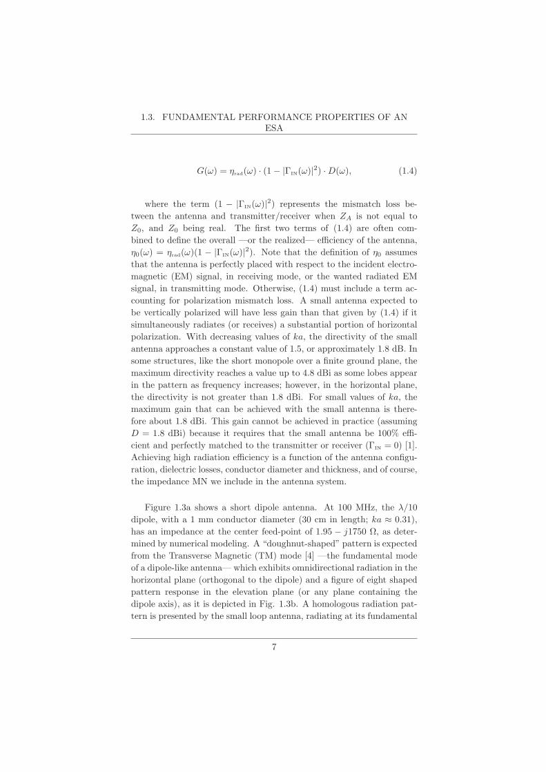
Figure 1.3a shows a short dipole antenna. At 100 MHz, the λ/10
dipole, with a 1 mm conductor diameter (30 cm in length; ka ≈ 0.31),
has an impedance at the center feed-point of 1.95 − j1750 Ω, as deter-
mined by numerical modeling. A “doughnut-shaped” pattern is expected
from the Transverse Magnetic (TM) mode [4] —the fundamental mode
of a dipole-like antenna— which exhibits omnidirectional radiation in the
horizontal plane (orthogonal to the dipole) and a figure of eight shaped
pattern response in the elevation plane (or any plane containing the
dipole axis), as it is depicted in Fig. 1.3b. A homologous radiation pat-
tern is presented by the small loop antenna, radiating at its fundamental
7

CHAPTER 1. INTRODUCTION
(a)
-20
-10
-30
(b)
Figure 1.3: Short dipole example. (a) Dimensions, impedance, and
current distribution. (b) Radiation pattern and gain.
Transverse Electric (TE) mode, but the omnidirectional projection relies
on a plane containing the loop.
An intrinsic quantity of interest for an ESA is the Q factor, defined
by Harrington in [14] as
Q =2 · ω0 ·max(WE ,WM )
PA, (1.5)
where WE and WM are the time averaged stored electric and mag-
netic energies, and PA is the antenna received power. The radiated power
is directly related to the received power through Prad = η0PA, where η0is the antenna total efficiency, defined in (1.2). It is assumed in (1.5)
that the small antenna is tuned to resonance at the frequency ω0, either
through self-resonance or by using a lossless reactive tuning element (an
inductor or a capacitor). Antenna Q is a quantity of interest and can
be also evaluated using equivalent circuit representations of the antenna.
Another important characteristic of Q is that it is inversely proportional
to antenna impedance bandwidth (approximately). A commonly used
approximation between Q and the 3 dB Fractional Bandwidth (FBW)
of the antenna, according to [2] is given by
8

1.4. ACTIVE CIRCUITS APPLIED TO IMPEDANCE MATCHING
Q ≈ 1
FBW3 dBfor Q � 1. (1.6)
There is a fundamental relation between the antenna size and the Q
of the antenna, expressed through the well-known equation Q = 1/(ka)3
[13], however, significant corrections and modifications have been made
as the result of an opened debate, which has taken place for many
years [2, 4, 5, 15]. A more detailed description of this relation is pre-
sented in Chapter 2; nevertheless, what is important to notice here is
the fact that as the more the antenna size decreases, the more difficult is
to match the antenna over an arbitrary bandwidth, because this latter
itself is limited, at the same time, by the antenna Q-factor. The high-Q
inherent to small antennas can be mitigated by including losses in the
antenna structure, or in the impedance matching, but at the expenses
of reducing the radiation efficiency. Then, an ESA can be matched with
a lossless MN, but only over very narrow bandwidths, according to the
Bode [11], Fano [12], and Youla [16] gain-bandwidth criterion, limiting
the performance of the transmitting/receiving system.
It is precisely at this last point where one of the most challenging
issues rises up, such as to achieve broadband impedance performance
on ESAs. It is, perhaps, the one that most interest has risen in ESA
design since, in general, an antenna always needs an impedance matching
network in practical use. As it is well-documented in the literature [1–4],
achieving impedance matching at the feed terminals of an ESA is a
crucial problem, because of the need to compensate its highly reactive
impedance with low loss, and to transform its low resistive impedance
to the load/system characteristic impedance (e.g. 50 Ω).
1.4 Active Circuits Applied to Impedance Matching
In the last decades, a notable improvement in circuit technology has
been evidenced throughout the race in increasing integration and avail-
ability of electronic components. What if somehow the same technology
could be applied to antennas? This inquisitiveness has led to an alter-
native way of designing ESAs, as it is the case of the varactor-based
tunable antennas and the even more attractive: antennas matched with
active non-Foster networks.
9

CHAPTER 1. INTRODUCTION
NIC
I2
ZL
ZNIC= -K(ZL)
I1
V1 V2
+ +
Port 1 Port 2
(a)
ZL
ZNICR1R2
Port 1 Port 2
(b)
Figure 1.4: (a) Block scheme of a NIC. (b) A typical grounded
topology of a BJT-based NIC proposed by Linvill [19].
Since the passive matching approach in an ESA is strongly limited by
the gain-bandwidth constraint, mentioned above, and by the maximum
achievable bandwidth constraint for a small-size antenna (imposed by
Wheeler [10], Chu [13] and Thal [17] criteria), active-matching technique
has become a very active topic during the last years. All the authors have
taken advantage of the negative-slope property of the reactance response
in non-Foster elements, and have tried to use it in order to compensate
the natural reactance of the antenna, not only at one single frequency
but over larger bandwidths. A non-Foster network/circuit (NFC) is a
two-terminal device which has an impedance function that does not obey
any of the three consequences of Foster’s reactance theorem [18]. This
theorem states that for a lossless passive two-terminal device, the slope of
its reactance (and susceptance) plotted versus frequency must be strictly
positive. The consequences derived from the theorem can be used to
classify an element or a circuit as Foster or non-Foster, by analyzing
its impedance function in the Laplace domain (s = σ + jω). These
consequences, besides a more detailed description of the theorem itself,
are given in Chapter 2.
NFCs have to be implemented with active devices; thus, they are
themselves active devices also, in the sense that they consume energy
from a power supply other than the signal source.
Non-Foster elements (called negative capacitors or negative induc-
tors) are implemented using two-port active circuits called Negative Im-
pedance Converter (NIC) [19], or Negative Impedance Inverter (NII) [20],
according to their set-up or topology, as it will be shown later. A NIC
10
1.4. ACTIVE CIRCUITS APPLIED TO IMPEDANCE MATCHING
circuit implements negative impedance, ZNIC = −k · ZL, for k > 0 with
ZL being the impedance to be converted, as it is depicted in Fig. 1.4a.
In the case of a NII, the input impedance, ZNII, results in a negated ver-
sion of the admittance associated to the load ZL, thus, ZNII = −k · YL,
for k > 0. NFCs have been considered since the 1950s when Linvill [19]
and Yanagisawa [21] introduced the first tested NIC topologies, like the
one depicted in Fig. 1.4b. A NIC is a two-port network implemented via
a combination of active devices (amplifiers or tunneling diodes), lumped
loads (capacitors and inductors) and supportive elements (resistors, RF
chokes, connections, etc.).
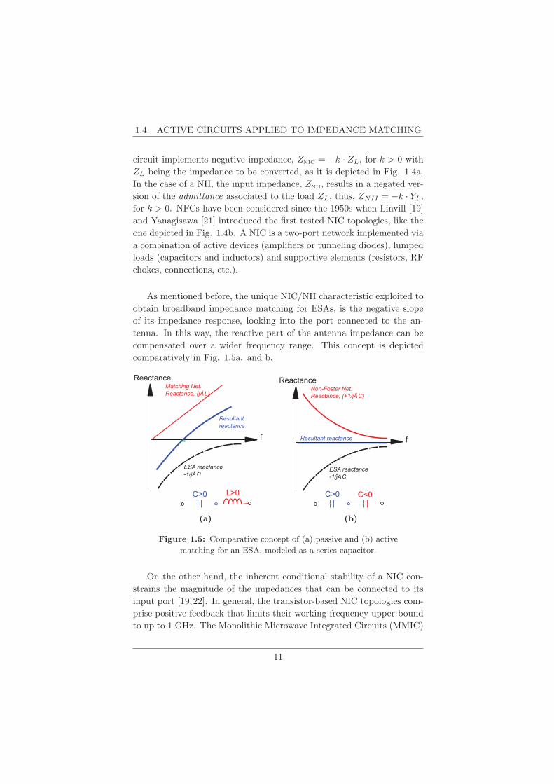
As mentioned before, the unique NIC/NII characteristic exploited to
obtain broadband impedance matching for ESAs, is the negative slope
of its impedance response, looking into the port connected to the an-
tenna. In this way, the reactive part of the antenna impedance can be
compensated over a wider frequency range. This concept is depicted
comparatively in Fig. 1.5a. and b.
ReactanceMatching Net.Reactance, (jĀL)
f
ESA reactance-1/jĀC
Resultant reactance
L>0C>0
(a)
C<0
ReactanceNon-Foster Net.Reactance, (+1/jĀC)
f
ESA reactance-1/jĀC
Resultant reactance
C>0
(b)
Figure 1.5: Comparative concept of (a) passive and (b) active
matching for an ESA, modeled as a series capacitor.
On the other hand, the inherent conditional stability of a NIC con-
strains the magnitude of the impedances that can be connected to its
input port [19,22]. In general, the transistor-based NIC topologies com-
prise positive feedback that limits their working frequency upper-bound
to up to 1 GHz. The Monolithic Microwave Integrated Circuits (MMIC)
11

CHAPTER 1. INTRODUCTION
can help but make the design process expensive and complicated [23].
Therefore, an exhaustive analysis of the stability is more than welcome.
It must take into account not only the transistor model but parasitics
and the antenna itself.
Further considerations should be considered, regarding, for example,
the added noise. Antennas with embedded non-Foster networks, in this
context, while using in receiving mode, have added noise due to the
active elements composing the NFCs. This noise degrades the Signal to
Noise Ratio (SNR), in addition to the bandwidth improvement of the
antenna system (NFC + Antenna). The SNR improvement (or possible
decrease) in the non-Foster matched antenna has to be measured in order
to characterize its performance completely when included in a receiver
system.
In most of the work reported, a cascade NIC + Antenna configura-
tion has been used. This condition implies a significant inconvenient in
using the active circuit, as this sort of transistor-based circuits are uni-
directional in some configurations, whereas an antenna is bidirectional.
Moreover, in transmitting mode, the NIC shall drive all the voltage and
current levels, which can derive in saturation or damage. Hence, the
classical application is limited to either transmitting or receiving. Thus,
any approach that allows the engineer to unify the design process will
be advantageous since other drawbacks in active matching design can
be addressed such as realizability, DC biasing and stability of the whole
antenna system (Antenna + NIC). This is the case of small antennas em-
bedded with NFCs (active-MNs), according to the approach developed
in this dissertation.
1.4.1 Possible Applications of Actively Matched Small
Antennas
In general, ESAs with embedded active MNs can be applied to any
application where a wide instantaneous impedance bandwidth is needed,
as well as when a reduction in the RF power needed from the system at
the radiation stage.
One interesting area to apply new designs and advances in antenna
miniaturization is the aeronautical industry. Airborne navigation and
12

1.5. MOTIVATION, OBJECTIVES AND CONTRIBUTION
communication systems need for wideband, light and low-drag (short)
antennas in their front-end. Currently used systems operate at the VHF
and the lower bound of the UHF bands, where the typical sizes asso-
ciated to the utilized antennas comprises some conventional blade-type
monopoles with around 45 cm in height (see Fig. 1.2d), for the lower
work frequency bands (down to 30 MHz). Those antennas correspond to
a factor ka between 0.19 and 0.22 for the Air Traffic Control (ATC) band,
or down to 0.05 for the radio links in the 30-88 MHz range. In these aero-
nautical systems, two different strategies have been implemented to over-
come the performance limitations inherent to the involved ESAs. The
first one consists of a passive and lossy MN based on lumped elements
such as toroidal ferrites, resistors, and capacitors, connected somehow
inside the antenna structure as a distributed MN. The second strategy
consists of implementing an electronically-tuned antenna (also called ac-
tive antenna in aeronautical jargon), typically by means of solid-state
switching devices (e.g. PIN diodes). This latter alternative implies some
extra control units to switch between one channel to another with up
to 10 MHz per channel bandwidth, unlike the instantaneous wideband
achievable with actively-matched ESAs, in which no extra control units
are needed.
Some other applications can be listed, such as civil security equip-
ment (e.g. the Terrestrial Trunked Radio (TETRA) band) and ve-
hicle communications, where embedded active matching designs allow
the development of VHF/UHF wideband antennas. In these antennas,
an effective-gain improvement can be provided by connecting an active
MN. Furthermore, other advantages can be obtained like better cov-
erage, compact size and reduced power consumption, by requiring less
transmission power for achieving the same coverage, compared with the
current passive antennas.
1.5 Motivation, Objectives and Contribution
As mentioned earlier, the limited electrical performance of ESAs, ag-
gravated by the rapidly developing communications world, has encour-
aged the antenna engineers’ community to propose alternative paths to
tackle the physical limitations of this type of radiating structures. Ac-
tive devices have been found to be a possible solution in some of those
13
CHAPTER 1. INTRODUCTION
alternative paths. In that sense, this dissertation is focused on con-
tributing to the antenna community with some additional observations,
and a systematic design methodology for ESAs loaded with NFC. As
a major contribution, a novel parameter for the proper location of the
NFC within the antenna structure, called Sensitivity Parameter (Sens),
is introduced and applied to real designs. The entire work is intended
to serve as an additional source of considerations for actively-matched
ESAs loaded with non-Foster elements.
Some specific objectives, associated to this dissertation, can be listed
as follows.
To develop a strategy for the efficient and systematic design of elec-
trically small antennas with a multiband or broadband operation.
To establish a technique of impedance matching, based on active
non-Foster-type networks embedded in the antenna structure itself.
To explore the possible improvement of critical antenna parame-
ters such as radiation efficiency and stability of the small actively
matched antennas.
To implement, by prototyping, such antenna systems comprising
antenna + active-MN with non-Foster elements.
1.6 Organization of the Dissertation
This thesis offers firstly a brief introduction to the ESA characteris-
tics, its applications and the description of the active impedance match-
ing strategy as a smart miniaturization technique. This, alongside some
motivation and organization words in Chapter 1. The fundamental char-
acteristics of antennas are presented at the beginning of Chapter 2, as
part of an overview of the definition, and the main characteristics, of
the most typical ESA structures as radiators. The most relevant limita-
tions and the methods conventionally used to match its impedance over
wider bandwidths are also shown. A review of the literature concerning
the most remarkable reported work in active matching alternatives and
techniques applied for antennas is included as well.
14

1.6. ORGANIZATION OF THE DISSERTATION
Chapter 3 deals with relevant criteria and design considerations in-
volved with the active impedance matching of an ESA, using such a
non-Foster networks, by means of a novel parameter, introduced by
the author, called sensitivity (Sens). This new parameter is analyti-
cally developed and applied to different antenna types, aimed at finding
the most advantageous location for a NFC. Relevant considerations re-
garding the realizability of the analytically-found impedances needed to
have wider impedance bandwidth are presented. Those analytically de-
rived impedances have a behavior inherently non-Foster that must be
addressed with active circuits.
Chapter 4 is devoted to present a complete design strategy of small
antennas, actively loaded with non-Foster elements. This strategy aims
at proposing a systematic methodology which includes: analytical find-
ing of both the NFC location and the required non-Foster impedance
for wideband matching, active-device selection to implement the NFC,
a statistical analysis about the effect of tolerance in components and
other manufacturing parameters over the global impedance and stabil-
ity performance. Current distribution analysis and the analysis of sta-
bility, through the Normalized Determinant Function (NDF) approach,
are also contemplated by the proposed strategy.
Chapter 5 presents, as a prospective of future work, the effect of the
inclusion of an active non-Foster network in the impedance matching of
a phased array. Finally, the main conclusions and future working lines
are presented in Chapter 6. The list of contributions resulting from the
development of this dissertation is shown in the Publications section at
the end of this document.
15


CHAPTER 2
IMPEDANCE MATCHING TECHNIQUESFOR ESAS: BACKGROUND
2.1 Fundamental Parameters of Antennas
To begin, in this section, the main parameters of antennas are briefly
reviewed. These parameters are explained in a simplified way, but there
exists a huge amount of books where the reader can go into further detail
of any of them [1,24–26].
2.1.1 Radiation Pattern
A radiation pattern is a representation of the radiated field by an
antenna as a function of the different directions of the space at a fixed
distance. Normally, spherical coordinates (r, θ, φ) are used and the
representation is referred to the electric field. As the electric field is of
vectorial type, two orthogonal components at each point of the constant
radius sphere, defined by the spherical coordinates, must be calculated
(usually θ and φ). Field radiation pattern or power radiation pattern
have the same information since power density (in the far field) is pro-
portional to the square of the electric field module, and when they are
represented in dB they are equal.
CHAPTER 2. MATCHING TECHNIQUES FOR ESAS
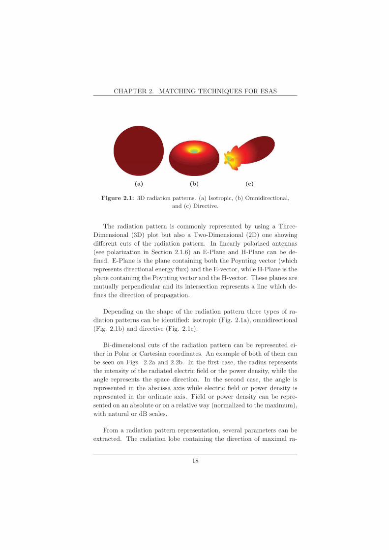
(a) (b) (c)
Figure 2.1: 3D radiation patterns. (a) Isotropic, (b) Omnidirectional,
and (c) Directive.
The radiation pattern is commonly represented by using a Three-
Dimensional (3D) plot but also a Two-Dimensional (2D) one showing
different cuts of the radiation pattern. In linearly polarized antennas
(see polarization in Section 2.1.6) an E-Plane and H-Plane can be de-
fined. E-Plane is the plane containing both the Poynting vector (which
represents directional energy flux) and the E-vector, while H-Plane is the
plane containing the Poynting vector and the H-vector. These planes are
mutually perpendicular and its intersection represents a line which de-
fines the direction of propagation.
Depending on the shape of the radiation pattern three types of ra-
diation patterns can be identified: isotropic (Fig. 2.1a), omnidirectional
(Fig. 2.1b) and directive (Fig. 2.1c).
Bi-dimensional cuts of the radiation pattern can be represented ei-
ther in Polar or Cartesian coordinates. An example of both of them can
be seen on Figs. 2.2a and 2.2b. In the first case, the radius represents
the intensity of the radiated electric field or the power density, while the
angle represents the space direction. In the second case, the angle is
represented in the abscissa axis while electric field or power density is
represented in the ordinate axis. Field or power density can be repre-
sented on an absolute or on a relative way (normalized to the maximum),
with natural or dB scales.
From a radiation pattern representation, several parameters can be
extracted. The radiation lobe containing the direction of maximal ra-
18
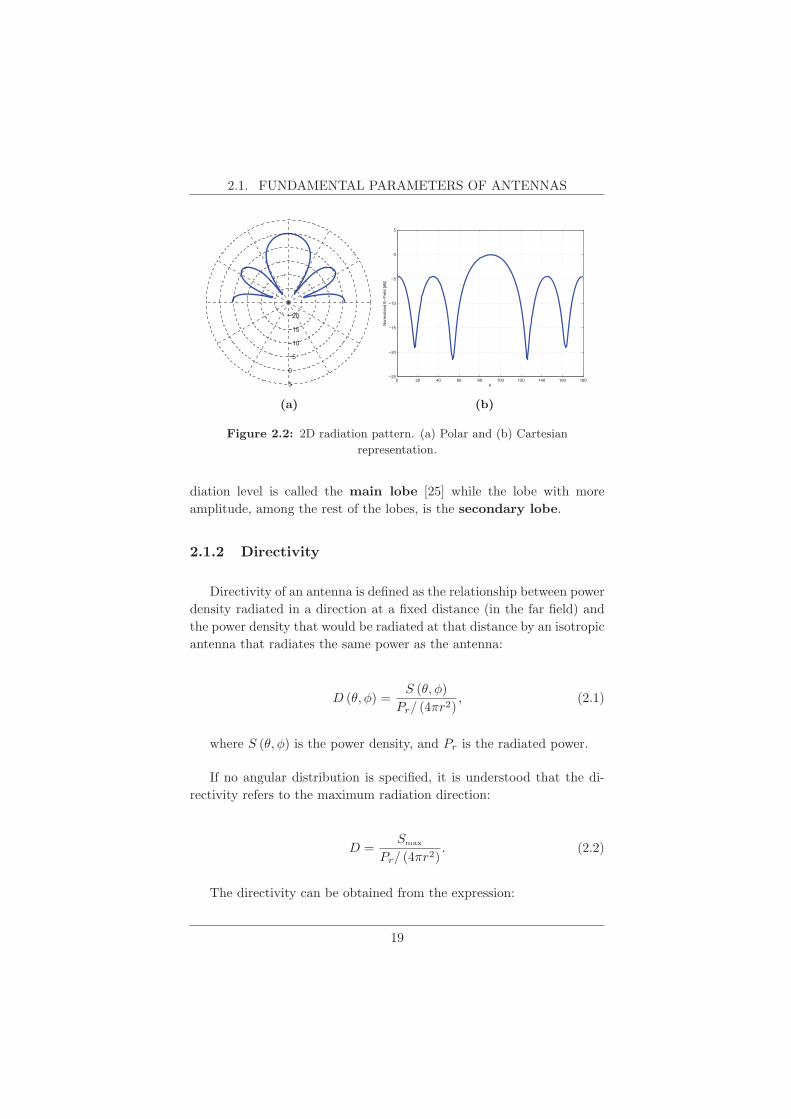
2.1. FUNDAMENTAL PARAMETERS OF ANTENNAS
−20
−15
−10
−5
0
5
(a)
0 20 40 60 80 100 120 140 160 180−25
−20
−15
−10
−5
0
5
θN
orm
aliz
ed E
−Fie
ld [d
B]
(b)
Figure 2.2: 2D radiation pattern. (a) Polar and (b) Cartesian
representation.
diation level is called the main lobe [25] while the lobe with more
amplitude, among the rest of the lobes, is the secondary lobe.
2.1.2 Directivity
Directivity of an antenna is defined as the relationship between power
density radiated in a direction at a fixed distance (in the far field) and
the power density that would be radiated at that distance by an isotropic
antenna that radiates the same power as the antenna:
D (θ, φ) =S (θ, φ)
Pr/ (4πr2), (2.1)
where S (θ, φ) is the power density, and Pr is the radiated power.
If no angular distribution is specified, it is understood that the di-
rectivity refers to the maximum radiation direction:
D =Smax
Pr/ (4πr2). (2.2)
The directivity can be obtained from the expression:
19

CHAPTER 2. MATCHING TECHNIQUES FOR ESAS
D (θ, φ) =4π∫∫
4πt (θ, φ) dΩ
, (2.3)
where
t (θ, φ) =S (θ, φ)
Smax
, (2.4)
is the normalized radiation pattern.
In directive antennas, a good approximation to calculate the direc-
tivity is:
D =4π
Δθ1 ·Δθ2, (2.5)
where Δθ1 and Δθ2 are the Half Power Beamwidth (HPBW) in the
two main planes of the radiation pattern.
Once the maximum directivity D and the normalized radiation pat-
tern t (θ, φ) are known, then it is easy to obtain the directivity at any
direction:
D (θ, φ) = D · t (θ, φ) . (2.6)
2.1.3 Gain
The gain, frequently denoted as the antenna gain (GA), is directly
related with directivity. Its definition is the same as the directivity one,
but instead of comparing with the radiated power, the actual delivered
power is used. Then, it is possible to take into account the losses of the
antenna (ηrad(ω) in Eq. (1.2)). The directivity and the gain are related
by radiation efficiency (ηrad) as follows:
20

2.1. FUNDAMENTAL PARAMETERS OF ANTENNAS
GA (θ, φ) =P (θ, φ)
Pdelivered/ (4πr2)=
Pr
Pdelivered
· P (θ, φ)
Pr/ (4πr2)
= ηrad ·D (θ, φ) (2.7)
When other parameters are desired to be included in the calculation
of the antenna gain, such as the mismatching factor (1 − |Γin(ω)|2),polarization efficiency and aperture efficiency [27], Eq. (2.7) has to be
complemented to become the Realized Gain, where all the efficiencies
are still a proportionality factor between Directivity and Gain, for a real
antenna. Thus, the realized gain is given by
G (θ, φ) = ηrad · ηapert · ηpol · (1− |Γin|2) ·D (θ, φ) . (2.8)
3 dB Beamwidth (Δθ3dB) or HPBW is the angular distance be-
tween the directions where the power density radiation pattern is equal
to half the maximum.
Beamwidth Between Zeros (Δθc) or First Null Beamwidth
(FNBW) is the angular distance between the directions at which the
main lobe has a minimum.
Side-Lobe Levels (SLL) is the relation between the value of the ra-
diation pattern, in the direction of maximum radiation, and the value
of the radiation pattern in the direction of the secondary lobe. It is
normally expressed in dB.
Front-to-Back ratio (F/B) Radiation is the relation between the
value of the radiation pattern, in the direction of maximum radiation,
and the value of the radiation pattern in the opposite direction.
2.1.4 Effective Aperture Area and Aperture Efficiency
The effective aperture or effective area (Aeff ) is defined as the rela-
tion between the power that the antenna delivers to its load (in a matched
21
CHAPTER 2. MATCHING TECHNIQUES FOR ESAS
case, suppose antenna working in reception) and the power density of the
incident wave. It is related to the directivity by the following formula:
Aeff
D=
λ2
4π. (2.9)
Effective aperture cannot be higher than the antenna physical aper-
ture, so an aperture efficiency (ηaperture) that relates the effective area
(Aeff) and the physical area (Aphy) of the antenna can be defined:
ηaperture =Aeff
Aphy
. (2.10)
2.1.5 Phase Pattern and Phase Center
Under some circumstances it is desirable to plot not the amplitude
of the electric field (as in the radiation pattern) but the phase of the
electric field. Such representation is called the phase pattern.
When observing an antenna at a great distance (i.e. in the far field),
its radiation can be seen as coming from a single point. In other words,
its wave front is spherical. This point, center of curvature of the surface
aperture with constant phase, is called the phase center of the antenna.
2.1.6 Polarization
Polarization represents the electric field vector orientation in a fixed
point as a function of time. It can be identified by the geometric fig-
ure described, as time goes, by the end of the electric field vector in
a fixed point of the space in the perpendicular plane to the propaga-
tion direction. Three figures can be generated: an ellipse (which is the
most generic one), a segment (linear polarization) and a circumference
(circular polarization).
The direction of rotation of the electric field vector, either in circu-
larly polarized waves or elliptically ones, it is called right-hand polariza-
tion if it is clockwise and left-hand if it is counterclockwise, looking from
the source of radiation.
22

2.1. FUNDAMENTAL PARAMETERS OF ANTENNAS
Axial ratio of an elliptically polarized wave is defined as the ratio
between the major and minor axis of the ellipse. It takes values between
1 and infinity. For a circularly polarized wave the axial ratio is 1.
2.1.7 Input Impedance
The input impedance of an antenna is the relation between the volt-
age and the current at the feed point of the antenna. It is normally a
complex number that depends on the frequency:
ZIN (ω) = R (ω) + jX (ω) . (2.11)
If X (ω) = 0 at some specific frequency, it is said that the antenna is
resonant at that frequency. Knowing the input impedance of an antenna
is a key factor because the antenna is usually connected to a transmission
line or to an active device (transistor, diode, etc.). If a mismatch occurs
between the antenna and the device, then not all the power transmitted
through the device will be delivered to the antenna (in transmitting
mode) or not all the power received by the antenna will be delivered to
the device (in receiving mode).
2.1.8 Radiation Resistance
When delivering power to an antenna, a part of it is radiated through
the free-space. This quantity can be defined by a radiation resistance
Rr which is defined as the equivalent resistance value that will dissipate
the same amount of power than that is radiated by the antenna:
Pr = I2 ·Rr. (2.12)
Not all the power delivered to an antenna is radiated through the free-
space. Associated to this, the loss resistance (also called ohmic losses),
Rl, can be defined. This resistance refers to the losses that appear in
23

CHAPTER 2. MATCHING TECHNIQUES FOR ESAS
the antenna and is defined as the resistance value that will dissipate the
same amount of power as the one not radiated by the antenna.
Pdelivered = Pr + Plosses = I2 ·Rr + I2 ·Rl. (2.13)
This is related to the radiation efficiency (ηrad) defined previously:
ηrad =Pr
Pdelivered
=Pr
Pr + Plosses
=Rr
Rr +Rl. (2.14)
2.1.9 Bandwidth
Bandwidth represents the frequency interval where one particular
property is satisfied. For the antenna case, two different kinds of param-
eters can be considered: impedance parameters or radiation parameters.
Then, the antenna bandwidth would be defined as the frequency margin
at which the impedance, or the reflection coefficient, is kept under some
value and the shape radiation pattern is kept constant. It can be repre-
sented as the absolute value (fmax − fmin) or as a relative one, FBW, as
follows:
FBW =fmax − fmin
f0. (2.15)
For broadband antennas, it is common to represent the bandwidth
in the form:
BW =fmax
fmin
: 1. (2.16)
The criteria used to determine the bandwidth of an antenna are re-
lated to the radiation pattern (directivity, polarization purity, beam-
width, SLL) or to the impedance (input impedance, reflection coefficient
or Voltage Standing Wave Ratio (VSWR)).
24
2.2. A BRIEF HISTORY OF ELECTRICALLY SMALLANTENNAS
2.2 A Brief History of Electrically Small Antennas
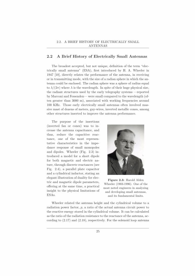
The broadest accepted, but not unique, definition of the term “elec-
trically small antenna” (ESA), first introduced by H. A. Wheeler in
1947 [10], directly relates the performance of the antenna, in receiving
or in transmitting mode, with the size of a radian sphere in which the an-
tenna could be enclosed. The radian sphere was a sphere of radius equal
to λ/(2π) where λ is the wavelength. In spite of their huge physical size,
the radiant structures used by the early telegraphy systems —reported
by Marconi and Fessenden— were small compared to the wavelength (of-
ten greater than 3000 m), associated with working frequencies around
100 KHz. Those early electrically small antennas often involved mas-
sive mast of dozens of meters, guy-wires, inverted metallic cones, among
other structures inserted to improve the antenna performance.
Figure 2.3: Harold Alden
Wheeler (1903-1996). One of the
most noted engineers in analyzing
and developing small antennas,
and its fundamental limits.
The purpose of the insertions
(inverted fan or cones) was to in-
crease the antenna capacitance, and
thus, reduce the capacitive reac-
tance, one of the most represen-
tative characteristics in the impe-
dance response of small monopoles
and dipoles. Wheeler (Fig. 2.3) in-
troduced a model for a short dipole
for both magnetic and electric na-
ture, through discrete reactances (see
Fig. 2.4), a parallel plate capacitor
and a cylindrical inductor, stating an
elegant illustration of duality for elec-
tric and magnetic dipole parameters,
offering at the same time, a practical
insight to the physical limitations of
ESAs.
Wheeler related the antenna height and the cylindrical volume to a
radiation power factor, p, a ratio of the actual antenna circuit power to
the reactive energy stored in the cylindrical volume. It can be calculated
as the ratio of the radiation resistance to the reactance of the antenna, ac-
cording to (2.17) and (2.18), respectively. For the solenoid loop antenna
25
CHAPTER 2. MATCHING TECHNIQUES FOR ESAS
(a) (b)
Figure 2.4: Reactive antenna model introduced by Wheeler [10] for (a)
a capacitor and (b) an inductor, occupying equals cylindrical volumes
—the short magnetic dipole— Rm = 320N2π6(a/λ)4 is the associated
radiation resistance, where N is the number of turns of the solenoid, and
a and b are the dimensions according to Fig. 2.4. The inductance of
the solenoid loop antenna is L = μ0N2(πa2/b), where μ0 is the perme-
ability of free-space. For the parallel plate capacitor —the short electric
dipole— the radiation resistance is given by Re = 80π2(b/λ)2. The ca-
pacitance, in this case, can be calculated by C = ε0πa2/b, where ε0 is
the permittivity of free-space.
pm =Rm
ωL=
4
3
π3a2b
λ
3
, (2.17)
pe = ReωC =4
3
π3a2b
λ
3
. (2.18)
The radiation power factor for an ESA is very small, since it is in-
versely related with the third power of the wavelength [2]. For example,
in the short dipole shown in Fig. 1.3a, whose length is 30 cm and its
diameter is 1 mm; the radiation factor pe drops down to 3.7 · 10−7,
approximately.
An additional definition, given by King in 1956 [28], referred to an
ESA as an antenna having the length and size in terms of the product
ka ≤ 0.5, where a is the radius of the smallest sphere enclosing all the
radiating structure, as it was depicted in Fig. 1.1, and k is the free-
space wave-number (k = 2π/λ). Thus, a = (1/2)(λ/2π), differs from
the radiansphere described by Wheeler, where a = λ/2π, by a factor of
2. In this sense, it is possible to say that the minimum enclosing sphere
26

2.3. CLASSIFICATION AND MOST TYPICAL ESASTRUCTURES
where the factor ka ≤ 0.5 is a reasonable bound for an ESA, in terms of
the free space wavelength, although several authors still use the classical
Wheeler’s condition. A value of ka = 0.5 represents an overall spherical
volume equal to λ3/48π2.
2.3 Classification and Most Typical ESA Structures
Some authors have preferred some elaborated, but not very extended,
classification of small antennas with categories depending, for example,
on the situation of the practical application. These categories include:
Electrically Small Antenna (ESA), when the classification parameter is
exclusively the wavelength at the working frequency; the Physically Con-
strained Small Antenna (PCSA), when the antenna, does not have di-
mensions of ESA, but a part of which has dimensions corresponding
to an ESA. Then, the Functionally Small Antenna (FSA), when the
antenna is engineered to enhance some performance toward lower fre-
quencies but with its size kept unchanged. This last one is the case of
those antennas in which the engineer tries to expand down in frequency,
for example, the impedance matching by including slots, near field par-
asitics, resonators, metamaterial particles etc. Finally, the Physically
Small Antenna (PSA), applicable specially to millimeter wave and Tera-
hertz (THz) applications, where manufacturing and characterizing such
small structures are challenging tasks [3].
In a more classical sense, with a conventional understanding of an-
tennas, it is possible to divide ESAs into two types. First, an electric
element, which couples to the electric field and is referred to as a capac-
itive antenna, as the one analyzed by Wheeler in Fig. 2.4a. Second, the
magnetic element (electric loop), which couples to the magnetic field and
is referred to as an inductive antenna, as the one analyzed by Wheeler
in Fig. 2.4b. H. Hertz utilized a sort of those structures, shown in
Figs. 2.5a, and 2.5b, respectively, for his first radio wave transmission
experiment [29].
However, many practical antennas are some combination of these
two types, where we can include short monopoles, loaded dipoles, patch
antennas with inverted insertions, loop antennas with magnetic cores,
Dielectric Resonator Antennas (DRA), multi-blended conductors with
27

CHAPTER 2. MATCHING TECHNIQUES FOR ESAS
40 cm
(a) (b)
Figure 2.5: Hertz antennas used for his first radio wave transmission
experiments [29]. (a) Dipole. b) Loop resonator.
exotic shapes, and antennas with metamaterials inclusions. Many of
these structures have been implemented in practice, in spite of how ex-
otic or complicated their form might be. In most cases, a compromised
performance is achieved, in special when a broad impedance bandwidth
or high radiation efficiency is intended [30]. Some examples of different
structures, frequently performed as ESAs, are depicted in Fig. 2.6.
The re-engineering and creation of small antennas, as those men-
tioned above, have been accelerated rapidly in response to a global
trend of urgent demands, that has been raised by the growth of mobile
phone and wireless deployed systems. These constantly modified systems
take the electronics components to almost its highest performance limit,
nonetheless, the ESAs involved with them, in many cases, are working
without a well-optimized design. Thus, it is possible to say that only
the antenna can further improve the overall system performance.
Although the wide use of ESAs in current wireless systems, there are
still several remaining issues to deal with concerning the design method-
ology, efficiency, and practical applications. There is a duality in this
sense: the implementation of an ESA is a big and challenging problem
for engineers, and at the same time, engineers are called to gain new
skills and methods to develop useful and practical ESAs.
2.4 Performance Characteristics of ESAs
Despite of the multiple definitions and classifications for small anten-
nas, it is possible to state some characteristics intimately linked with the
28
2.4. PERFORMANCE CHARACTERISTICS OF ESAS
Ground Plane
(a) (b)
Substrate
Patch
GND
(c)
Ground PlanePort
Vias
(d)
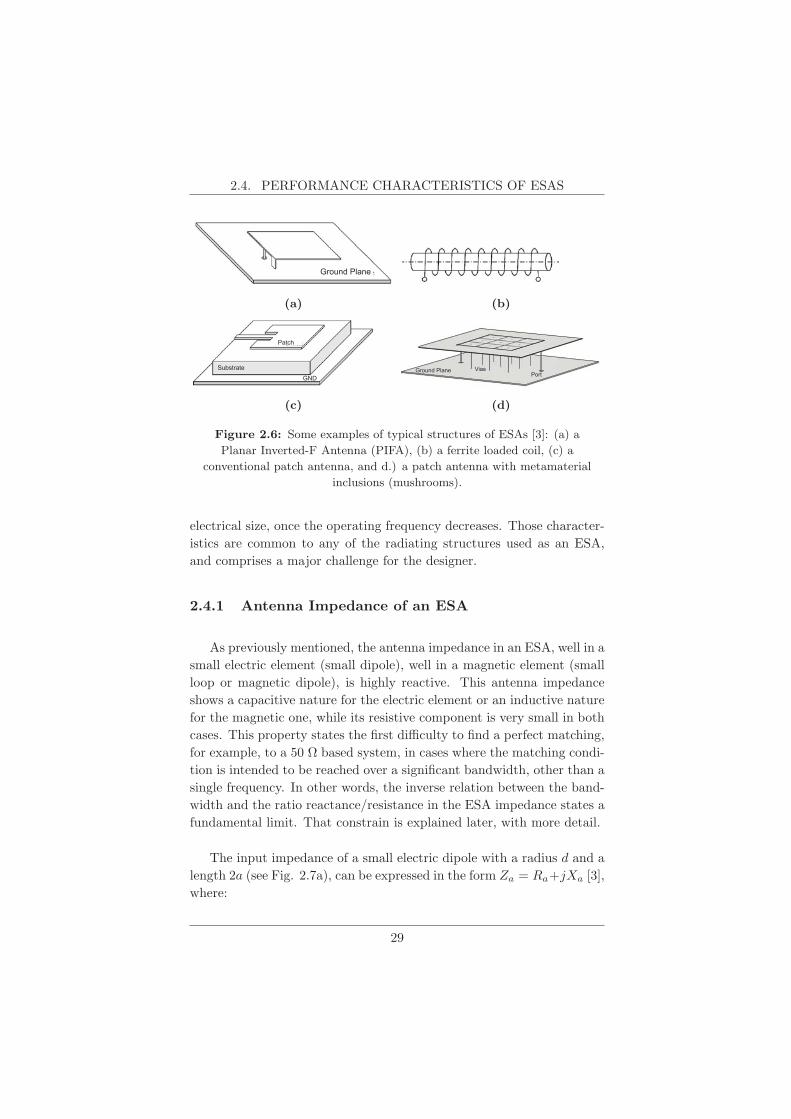
Figure 2.6: Some examples of typical structures of ESAs [3]: (a) a
Planar Inverted-F Antenna (PIFA), (b) a ferrite loaded coil, (c) a
conventional patch antenna, and d.) a patch antenna with metamaterial
inclusions (mushrooms).
electrical size, once the operating frequency decreases. Those character-
istics are common to any of the radiating structures used as an ESA,
and comprises a major challenge for the designer.
2.4.1 Antenna Impedance of an ESA
As previously mentioned, the antenna impedance in an ESA, well in a
small electric element (small dipole), well in a magnetic element (small
loop or magnetic dipole), is highly reactive. This antenna impedance
shows a capacitive nature for the electric element or an inductive nature
for the magnetic one, while its resistive component is very small in both
cases. This property states the first difficulty to find a perfect matching,
for example, to a 50 Ω based system, in cases where the matching condi-
tion is intended to be reached over a significant bandwidth, other than a
single frequency. In other words, the inverse relation between the band-
width and the ratio reactance/resistance in the ESA impedance states a
fundamental limit. That constrain is explained later, with more detail.
The input impedance of a small electric dipole with a radius d and a
length 2a (see Fig. 2.7a), can be expressed in the form Za = Ra+jXa [3],
where:
29

CHAPTER 2. MATCHING TECHNIQUES FOR ESAS
(a)
ln(2a/d)=20
1512.510
Rea
ctan
ce (Ā
)
Resistance (Ā
)
Xa Ra
ka
(b)
Figure 2.7: (a) Small electric dipole. (b) Impedance Za as a function
of the size factor ka [3]
Ra = 20(ka)2, (2.19)
Xa = 60
(ln
(2a
d
)− 3.39
)(1/ka) . (2.20)
Some curves, representing the reactance Xa for different values of
ln(2a/d), are shown in Fig. 2.7b. An important difference between the
real and the imaginary parts of Za is observed (up to six magnitude
orders) as the antenna size decreases.
A similar response is observed for the small magnetic element, rep-
resented by a small loop antenna with radius a and wire radius d, as
the one depicted in Fig. 2.8. The inductance of the small loop can be
computed as (2.22) [25], and can be depicted as a function or the ratio
a/d, as shown in Fig. 2.9a. The radiation resistance of the antenna,
which can be computed as (2.21), is depicted in Fig. 2.9b. Resistance
values lower than 10 Ω are observed for ka ≤ 0.5. For example, a loop
with radius a = 10 cm, and a wire radius d = 1 mm (a/d = 100), will
show an inductance of 0.59 μH. This loop antenna can be considered
small up to 238 MHz since the ka factor equals 0.5 at this frequency.
30
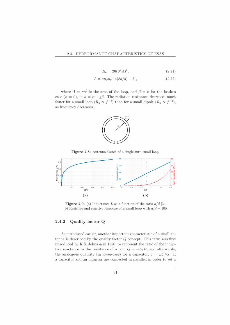
2.4. PERFORMANCE CHARACTERISTICS OF ESAS
Ra = 20(β2A)2, (2.21)
L = aμ0μr [ln(8a/d)− 2] , (2.22)
where A = πa2 is the area of the loop, and β = k for the lossless
case (α = 0), in k = α + jβ. The radiation resistance decreases much
faster for a small loop (Ra ∝ f−4) than for a small dipole (Ra ∝ f−2),
as frequency decreases.
Figure 2.8: Antenna sketch of a single-turn small loop.
(a)
Rea
ctan
ce (Ā
)
Rad
. Res
ista
nce
(Ā)750
250 5
15
(b)
Figure 2.9: (a) Inductance L as a function of the ratio a/d [3].
(b) Resistive and reactive response of a small loop with a/d = 100.
2.4.2 Quality factor Q
As introduced earlier, another important characteristic of a small an-
tenna is described by the quality factor Q concept. This term was first
introduced by K.S. Johnson in 1920, to represent the ratio of the induc-
tive reactance to the resistance of a coil, Q = ωL/R, and afterwards,
the analogous quantity (in lower-case) for a capacitor, q = ωC/G. If
a capacitor and an inductor are connected in parallel, in order to set a
31

CHAPTER 2. MATCHING TECHNIQUES FOR ESAS
tuned circuit, the power response decreases as a factor of 1/√2 when
the circuit is detuned by a fractional quantity δω/ω = 1/2Q. Then,
1/Q is the 3 dB bandwidth of the circuit. In a tuned radio terminal,
for example, the higher values for parameter Q were preferred to avoid
interferences with adjacent channels. By the beginning of the second
half of the past century, the factor Q became important to characterize
the resonance curve of resonators in radar and communications systems.
Figure 2.10: Lan Jen Chu
(1913-1973). Remarkable Professor
and IEEE Fellow.
If over a resistor R, associated
with the equivalent series resistance
of an inductor in a tuned parallel
LC circuit, with a resonant frequency
given by ω0 = 1/√LC, is flowing a
current I, then the average power dis-
sipated in the resistor, PL, is I2R/2.
The average energy stored in the
magnetic field around the inductor
is given by Wm = I2L/4. In addi-
tion, it is known that at resonance
the time-averaged energy stored in
the capacitor is equal to that in the
inductor. If we now use these into
the definition of Q by Johnson, it is
possible to derive an expression for Q as follows [2]:
Q =ωL
R=
2ω(I2L/4)
I2R/2=
2ωWm
PL=
ω(Wm +We)
PL
Q =ω(average energy stored in resonant circuit)
average energy dissipated per second. (2.23)
Equation (2.23) is a very commonly used definition for the Q of a
resonant circuit, and it can be extended for antennas in terms of the
antenna impedance around the resonant frequency [28], as follows:
Q ∼= ωdX/dω
2R. (2.24)
32
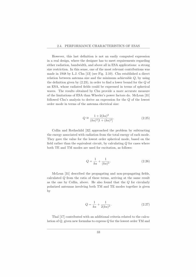
2.4. PERFORMANCE CHARACTERISTICS OF ESAS
However, this last definition is not an easily computed expression
in a real design, where the designer has to meet requirements regarding
either radiation, bandwidth, and above all in ESA applications: a strong
size restriction. In this sense, one of the most relevant contributions was
made in 1948 by L.J. Chu [13] (see Fig. 2.10). Chu established a direct
relation between antenna size and the minimum achievable Q, by using
the definition given by (2.23), in order to find a lower bound for the Q of
an ESA, whose radiated fields could be expressed in terms of spherical
waves. The results obtained by Chu provide a more accurate measure
of the limitations of ESA than Wheeler’s power factors do. McLean [31]
followed Chu’s analysis to derive an expression for the Q of the lowest
order mode in terms of the antenna electrical size:
Q ∼= 1 + 2(ka)2
(ka)3[1 + (ka)2]. (2.25)
Collin and Rothschild [32] approached the problem by subtracting
the energy associated with radiation from the total energy of each mode.
They gave the value for the lowest order spherical mode, based on the
field rather than the equivalent circuit, by calculating Q for cases where
both TE and TM modes are used for excitation, as follows:
Q =1
ka+
1
(ka)3. (2.26)
McLean [31] described the propagating and non-propagating fields,
calculated Q from the ratio of these terms, arriving at the same result
as the one by Collin, above. He also found that the Q for circularly
polarized antennas involving both TM and TE modes together is given
by
Q =1
ka+
1
2(ka)3. (2.27)
Thal [17] contributed with an additional criteria related to the calcu-
lation of Q, given new formulas to express Q for the lowest order TM and
33
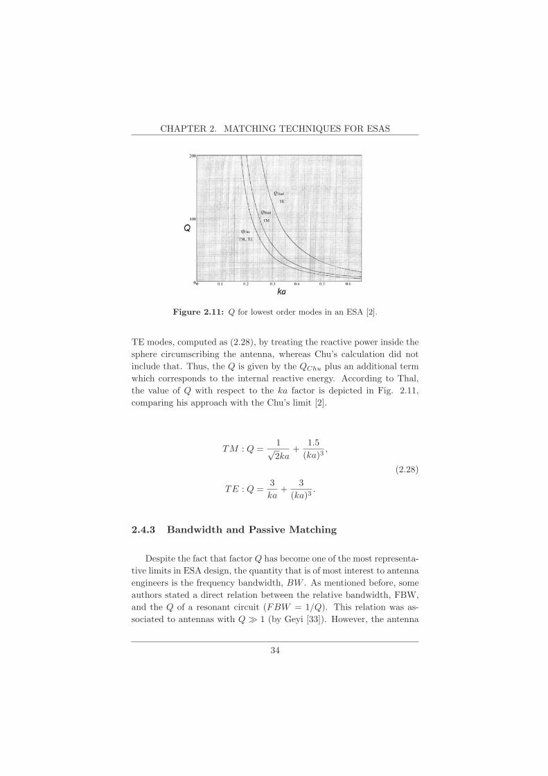
CHAPTER 2. MATCHING TECHNIQUES FOR ESAS
Figure 2.11: Q for lowest order modes in an ESA [2].
TE modes, computed as (2.28), by treating the reactive power inside the
sphere circumscribing the antenna, whereas Chu’s calculation did not
include that. Thus, the Q is given by the QChu plus an additional term
which corresponds to the internal reactive energy. According to Thal,
the value of Q with respect to the ka factor is depicted in Fig. 2.11,
comparing his approach with the Chu’s limit [2].
TM : Q =1√2ka
+1.5
(ka)3,
TE : Q =3
ka+
3
(ka)3.
(2.28)
2.4.3 Bandwidth and Passive Matching
Despite the fact that factor Q has become one of the most representa-
tive limits in ESA design, the quantity that is of most interest to antenna
engineers is the frequency bandwidth, BW . As mentioned before, some
authors stated a direct relation between the relative bandwidth, FBW,
and the Q of a resonant circuit (FBW = 1/Q). This relation was as-
sociated to antennas with Q � 1 (by Geyi [33]). However, the antenna
34

2.4. PERFORMANCE CHARACTERISTICS OF ESAS
bandwidth cannot simply be defined in the same way as in circuitry,
due to the existence of some limiting factors which limits the functional
bandwidth of the antenna. Among these factors it can be included, for
example, the change of the radiation pattern shape or direction, vari-
ation in the impedance characteristics, near field parasitics, change in
size, etc. In general, it is possible to define the bandwidth BW of an
antenna as a frequency range within which the antenna meets a given
set of specifications, typically based on the impedance or antenna gain
characteristics. For the ESA case, either the antenna input impedance
or the power spectra can be considered as the parameter to specify the
bandwidth [3].
It is possible to calculate the absolute BW as the difference between
the upper and the lower frequency bounds (f1 − f2); both specified to
meet certain value for parameters such as the VSWR or the Return Loss
(RL), which stands for the antenna impedance (Za) performance. Some
useful and well-known relations are given as follows:
ΓIN = (Za − Z0)/(Za + Z0), (2.29)
V SWR = (1 + ΓIN)/(1− ΓIN), (2.30)
RL = −20 log|ΓIN|, (2.31)
where ΓIN is the reflection coefficient looking into the driving point
of the antenna. Za and Z0 are the antenna and the characteristic
impedances, respectively.
The FBW is defined as the ratio of BW to the central frequency (f0)
of the band, that is: FBW = (f2−f1)/f0. This last expression is widely
used in antenna design. There is an important relation between band-
width and the Q factor for ESAs, as it was described by Yaghjian and
Best [15], who derived such relationship through the maximum allowable
VSWR, or s, as follows:
FBW ≈(
1
Q
)((s− 1)√
s
). (2.32)
35
CHAPTER 2. MATCHING TECHNIQUES FOR ESAS
2.4.4 Radiation efficiency
As aforementioned, as the antenna size decreases to ka-factor levels
much lower than 1, the resistive part of its input impedance drops to
levels of a few Ohms, or even less (see Figs. 2.7b and 2.9b). This con-
dition comprises a high difficulty in the impedance matching process, as
it will be shown below. If we now take in mind the losses in the antenna
structure, like those associated with lossy conductors or dielectric mate-
rials (e.g. in printed antennas), an additional issue arises as the decrease
in the antenna radiation efficiency.
The radiation efficiency ηrad is given by
ηrad = Prad/Pacc = Rrad/(Rrad +Rl), (2.33)
where Prad and Pacc are the radiated and the accepted powers, re-
spectively, and Rl represents both the losses in the antenna structure and
the added losses through a possible MN. In any antenna design, radiation
efficiency can be understood as the constant of proportionality between
directivity and gain, on account of the relation: Gmax = ηrad · Dmax.
Thus, special attention must be paid to the added losses in the design
of any kind of matching or tuning network for an ESA. Therefore, any
lossy material, lossy reactive element, or resistive equalization included
to fulfill the impedance matching of an ESA will degrade the radiation
efficiency.
2.5 Passive Impedance Matching Constraints
Considering the aforementioned characteristics of ESAs, a statement
can be claimed regarding that as the antennas reduce in size, the band-
width tends to be narrower and the gain and the efficiency will degrade.
Then, the question is: how small can an antenna be designed while still
being practical? From the radiation point of view, J. D. Kraus [26]
showed that a small antenna could have an effective aperture as high as
98 percent of that of a half-wave dipole antenna, if the antenna could
perfectly match the load. In fact, for both short dipoles and small loops,
36

2.5. PASSIVE IMPEDANCE MATCHING CONSTRAINTS
the directivity remains at 1.5 as the dimensions decrease. It suggests
that any ESA can transmit/receive almost the same amount of power
(only a small percent less) as a half-wavelength dipole does. In other
words, there would seem to be no limitation in reducing the antenna
size so far as the antenna could be perfectly matched.
Figure 2.12: Roberto Mario
Fano (1917-2016). Remarkable
Professor and IEEE Fellow.
It is precisely at this point where
the big challenge rises up, the perfect
matching is impossible when an an-
tenna becomes extremely small, be-
cause it is well known that large ca-
pacitive reactance in short dipoles
and large inductive reactance in small
loops are hard to match. In addition,
losses existing in the antenna and the
matching circuit will exceed the radi-
ation resistance, resulting in a signif-
icant reduction of the effective aper-
ture, that corresponds to a reduction
of the radiation power and degrada-
tion of the radiation efficiency.
The performance of a passive impedance MN is intimately bounded
up to the antenna input impedance (Za) behavior with the frequency. Za
becomes the load to the matching network itself (in the conventional cas-
cade/series approach). If the intended design comprises a small dipole-
type antenna, the input impedance can be modeled as a series connection
of a resistor and a capacitor, as depicted in Fig. 2.13a. If a lossless pas-
sive MN is used, there is a fundamental Gain-Bandwidth constraint limit
derived by H. Bode [11] and complemented by R.M. Fano [12] (see Fig.
2.12), and years later by Youla [16]. This limit states a relation between
a purely resistive generator and a complex and arbitrary passive load.
Given a maximum reflection coefficient magnitude, Bode-Fano integral
criterion can be expressed as the Gain-Bandwidth restriction on the load
within a flat pass-band. In others words, there is a tradeoff between the
achievable bandwidth and the maximum tolerable reflection coefficient
magnitude. The analytical expression, for the small dipole (series RC
circuit), is [34]:
37

CHAPTER 2. MATCHING TECHNIQUES FOR ESAS
2-portLosslessMatchingNetwork
R
C
Ā(Ā) Za
(a)
Ā(Ā)
ȀĀ
ĀĀ2Ā1
(b)
Figure 2.13: (a) Small dipole-like model loading a lossless MN. (b) A
possible response for Γ(ω), within a limited band Δω, given the value
Γm for a series passive RC [34].
∫ ∞
0
1
ω2ln
1
|Γ(ω)|dω < πRC. (2.34)
Once the maximum reflection coefficient magnitude is established,
the bandwidth is limited, and vice versa. Figure 2.13b shows this max-
imum tolerable reflection coefficient, Γm, over the bandwidth Δω =
ω2 − ω1, which is governed by the Bode-Fano limit. A mathematical
expression for the limit can now be written as [34]:
∫ ω2
ω1
1
ω2ln
1
|Γm|dω = Δω ln1
|Γm| ≤ πω20RC, (2.35)
where ω0 is the central frequency of the band of interest.
If the quality factor Qa = 1/(ωRC), associated with the antenna
model in Fig. 2.13a, is included in (2.35), it is possible to re-write this
expression as:
Δω ln1
|Γm| ≤ πω0/Qa. (2.36)
It is clear that a smaller Q factor results in a larger achievable band-
width. On the other hand, antenna miniaturization implies, as expected,
further limitations on the reflection coefficient, within the intended band.
38

2.6. IMPEDANCE MATCHING USING ACTIVE & NON-FOSTERNETWORKS
A simplification of (2.36) lead us to a more convenient expression:
exp
( −πω0
ΔωQa
)≤ |Γm| (2.37)
This equation demonstrates that the allowable reflection coefficient
can be lowered at the expense of the smaller bandwidth.
The equality in (2.35) can be satisfied by ideally including infinite
lossless sections in the matching network (MN). This fact leads, for ex-
ample, to a Bandwidth Improvement Factor (BWIF) of 3.8128, once
added the MN, if |Γm| is intended to be 0.33 (VSWR = 2). Nonetheless,
when including three sections of lossless reactive components, the BWIF
reaches an acceptable value of 3.1435 [2]. Hansen in [35], complementing
the Bode’s theory, introduced a useful expression to calculate the BWIF
in terms of Γ (or VSWR by using (2.30)), as follows:
BWIF =1− Γ2
2Γ
π
ln(1/Γ). (2.38)
This last estimation for the improvement in bandwidth by the action
of a multi-section MN does not take into account the introduced losses,
unavoidable in real applications, but provides the designer with some
theoretical criteria to be considered when a ESA is to be performed.
2.6 Impedance Matching Using Active & non-Foster
Networks
In this section, the most relevant characteristics and the evolution of
the concept of active matching applied for antennas is presented. The
two most important approaches are described as well as some relevant
work reported in the literature.
As described in the previous section, because of the natural con-
straints associated with their small size relative to their operating wave-
length, the impedance bandwidths associated with the most common
39
CHAPTER 2. MATCHING TECHNIQUES FOR ESAS
ESA structures are quite limited [13, 17]. Nevertheless, if it were possi-
ble, it would be highly desirable to achieve an ESA design working over a
wide instantaneous frequency interval, even when this task might imply
the use of active devices.
The main idea of adding active devices to a MN for an ESA is to
expand the impedance bandwidth of the antenna as much as possible,
beyond the bandwidth limits mentioned before, while maintaining the
fundamental performance expected from an antenna. Thus, besides the
intended wide impedance bandwidth, other basics characteristics such
as a practical gain value, a practical radiation pattern, and a moderate
difficulty in manufacturing, among others, are preferred. There are two
different approaches to carry out an active MN in ESAs: the tunable
realization and the non-Foster MN addition. Each of these approaches
can be implemented in two ways: embedded into the antenna structure
or in series/parallel configuration at the feed point of it. It is precisely
the embedded alternative the one developed in the most part of this
work.
In the first approach, the impedance matching of the ESA have ex-
ploited the tunability property of the antenna itself to perform it as a
tunable antenna, by means of some reconfigurable technology. For this
purpose, variable reactances —like varactor diodes— or a metamaterial
particle with the possibility of varying its shape or size have been used.
Those inclusions compensate the reactive part of the antenna impedance,
at a certain frequency, and modify the radiating element response. It is
worth noting that tunability —or reconfigurability— can be applied to
the frequency of operation, direction of the main beam, beamwidth, and
in general to one or more of the antenna parameters [36, 37].
In fact, the tunability property in an ESA is often checked out as a
preliminary stage of an active non-Foster MN design process, the sec-
ond approach mentioned above, especially in cases where the non-Foster
circuit (NFC) is intended to be embedded in the antenna structure. In
those cases, the tunability is checked with the purpose of observing the
antenna response to a change in the reactance/susceptance, at the se-
lected point where the active non-Foster form is going to be connected.
By using this technique, it is possible to prove, in an experimental way,
the need for a non-Foster element to compensate the antenna reactance
40

2.6. IMPEDANCE MATCHING USING ACTIVE & NON-FOSTERNETWORKS
over a significant frequency range [36, 38]. This fact leads us to a more
interesting alternative: the non-Foster implementation.
In this second approach, a variety of active circuits, called Negative
Impedance Converters (NICs), have been used as a smart alternative
to tackle the narrowband problem in ESA impedance matching. These
circuits where first proposed in the 1950’s by Linvill [19], but only have
been widely studied and applied to ESAs in the last years, as it will be
shown later. The behavior of the reactance presented by the NIC versus
the frequency —its negative slope— is the cornerstone in developing
non-Foster MNs and applying them to match ESAs. Many authors have
reported encouraging results by placing the NFC in the antenna feed
point [39–41]. Some others have reported practical designs by embedding
the NFC in the radiating element itself, well in a printed or planar ESA
[42, 43], well in a near-field structure or parasitic [38, 44], or in some
ground plate or chassis containing the radiating element [45,46].
Embedded or not, when an active non-Foster element acting as im-
pedance MN is added to an ESA, the basic idea remains as to overcome
the bandwidth restrictions of passive matching. These restrictions are
evidenced even when reconfigurable technologies are used, as it will be
shown below. Thus, the non-Foster MN approach stands for a way of
achieving wide instantaneous bandwidths in size-limited applications.
2.6.1 Tunable Antennas Technique
The tunable-antenna approach takes advantage of one important
property in some radiating structures: frequency agility (or tunability).
Tunability consist of obtaining additional narrow bands (even additional
radiating modes) by including variable reactances or by modifying other
parameters such as physical dimensions, substrate permeability or sub-
strate permittivity. Most of the reported work have been carried out
utilizing varactor-type diodes inserted in the antenna itself [36], or in
some parasitic [47] or metamaterial inclusion [48]. In many other cases
frequency-agile antennas using varactors have been proposed including
PIFAs [49–51], planar monopoles [36], slot dipoles [52], slot rings [53],
printed bow-ties [54] or quasi-Yagi [55], among others, making the varac-
tor one of the most versatile devices for implementing frequency agility.
41
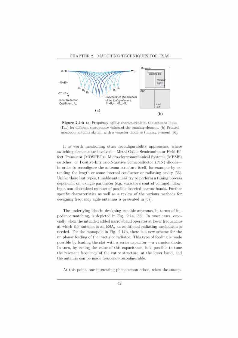
CHAPTER 2. MATCHING TECHNIQUES FOR ESAS
f
Input ReflectionCoefficient, Āin
0 dB
-10 dB
-20 dB
B1 B2 B3Bn-1
Bn
Susceptance (Reactance) of the tuning element.B1>B2>...>Bn-1>Bn
(a)
GND
InputPort
Varactordiode
Radiating slot
Monopole
(b)
Figure 2.14: (a) Frequency agility characteristic at the antenna input
(Γin) for different susceptance values of the tunning-element. (b) Printed
monopole antenna sketch, with a varactor diode as tunning element [36].
It is worth mentioning other reconfigurability approaches, where
switching elements are involved —Metal-Oxide-Semiconductor Field Ef-
fect Transistor (MOSFET)s, Micro-electromechanical Systems (MEMS)
switches, or Positive-Intrinsic-Negative Semiconductor (PIN) diodes—
in order to reconfigure the antenna structure itself, for example by ex-
tending the length or some internal conductor or radiating cavity [56].
Unlike these last types, tunable antennas try to perform a tuning process
dependent on a single parameter (e.g. varactor’s control voltage), allow-
ing a non-discretized number of possible inserted narrow bands. Further
specific characteristics as well as a review of the various methods for
designing frequency agile antennas is presented in [57].
The underlying idea in designing tunable antennas, in terms of im-
pedance matching, is depicted in Fig. 2.14, [36]. In most cases, espe-
cially when the intended added narrowband operates at lower frequencies
at which the antenna is an ESA, an additional radiating mechanism is
needed. For the monopole in Fig. 2.14b, there is a new scheme for the
uniplanar feeding of the inset slot radiator. This type of feeding is made
possible by loading the slot with a series capacitor —a varactor diode.
In turn, by tuning the value of this capacitance, it is possible to tune
the resonant frequency of the entire structure, at the lower band, and
the antenna can be made frequency-reconfigurable.
At this point, one interesting phenomenon arises, when the suscep-
42
2.6. IMPEDANCE MATCHING USING ACTIVE & NON-FOSTERNETWORKS
tance associated to the variable capacitor is analyzed, a decreasing be-
havior is observed as the frequency increases. This is the experimental
confirmation of the non-Foster nature of the admittance needed to match
the antenna all along the tuning range, which shall be placed at the slot.
As the needed susceptance decreases with frequency, according to the re-
lations B1 > B2, ..., Bn−1 > Bn in Fig. 2.14a, a regular passive capacitor
cannot fulfill the reactance compensation because its susceptance func-
tion, B = ωC, is directly proportional to the frequency. Thus, only a
negative capacitor would show the observed non-Foster behavior. Then,
the non-Foster susceptance should be BNF = ωCNF = −ωC. Identical
phenomenon is observed in a magnetic-type ESA, like a small loop, where
the reactance needed to match the antenna has a negative-slope induc-
tive nature, implying the necessity of implementing a negative inductor,
with a reactance function given by XNF = jωLNF = −jωL.
Among the limitations of tunable antennas, it can be mentioned their
losses and the non-linearity introduced by the tuning devices. As men-
tioned above, some authors carry out a tunable antenna design as a previ-
ous stage for applying a non-Foster MN, replacing the reactance-variable
element for a NFC which presents the same behavior of reactance versus
frequency.
2.6.2 Non-Foster Impedance Matching: Concept
As mentioned before, in cases where the application demands a broad
instantaneous bandwidth, the tunable approach does not fit this require-
ment. Then, a new dimension for ESA design field relies in the use of
non-Foster circuits, whose application arises from the necessity to over-
come the limitations in broad bandwidth matching shown in previous
sections.
The very basic idea of non-Foster matching for an electrically small
antenna is illustrated in Figs. 2.15(a, b). Figure 2.15a shows the con-
ventional first-order passive-matching approach, which looks for cancel-
ing the reactive part of the load to reach the condition of resonance
(Im{ZIN} = 0) at a unique frequency. In this first example, the load
consists of a mathematical model of a monopole-like ESA, as the one
depicted in the upper part of Fig. 2.15a. The single frequency of res-
onance occurs when the resultant reactance (dash-dotted blue curve)
43
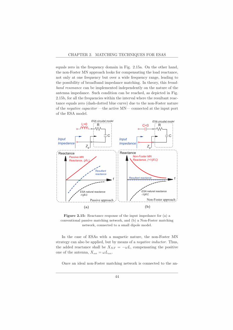
CHAPTER 2. MATCHING TECHNIQUES FOR ESAS
equals zero in the frequency domain in Fig. 2.15a. On the other hand,
the non-Foster MN approach looks for compensating the load reactance,
not only at one frequency but over a wide frequency range, leading to
the possibility of broadband impedance matching. In theory, this broad-
band resonance can be implemented independently on the nature of the
antenna impedance. Such condition can be reached, as depicted in Fig.
2.15b, for all the frequencies within the interval where the resultant reac-
tance equals zero (dash-dotted blue curve) due to the non-Foster nature
of the negative capacitor —the active MN— connected at the input port
of the ESA model.
ReactancePassive MNReactance, (jĀL)
f
ESA natural reactance-1/jĀC
Resultant reactance
R
C
Za
InputImpedance
L>0ESA circuital model
Passive approach
(a)
ReactanceNon-Foster MNReactance, (+1/jĀC)
f
ESA natural reactance-1/jĀC
Resultant reactance
R
C
Za
InputImpedance
C<0ESA circuital model
Non-Foster approach
(b)
Figure 2.15: Reactance response of the input impedance for (a) a
conventional passive matching network, and (b) a Non-Foster matching
network, connected to a small dipole model.
In the case of ESAs with a magnetic nature, the non-Foster MN
strategy can also be applied, but by means of a negative inductor. Thus,
the added reactance shall be XNF = −ωL, compensating the positive
one of the antenna, Xant = ωLant.
Once an ideal non-Foster matching network is connected to the an-
44
2.6. IMPEDANCE MATCHING USING ACTIVE & NON-FOSTERNETWORKS
tenna, the overall input reflection coefficient (see Fig. 2.15b) will be
mapped over the horizontal axis in the Smith chart, leading to a possi-
bly conjugate matching between the generator and the antenna, provided
equality in their impedance resistive parts, and therefore, the maximum
power transfer to the antenna [34]. It is important to note that the
inclusion of an ideal non-Foster matching network itself does not imply
maximum power transfer to the antenna, however, this can be partially
fulfilled by matching two different resistive parts only, then an improve-
ment in the antenna gain and total efficiency can be expected afterward.
2.6.3 Foster’s Reactance Theorem and non-Foster Ele-
ments
Foster’s reactance theorem [18] is a consequence of the conservation of
energy principle. It states that for a lossless passive two-terminal device,
the slope of its reactance (and susceptance) plotted versus frequency
must be strictly positive. In other words, the frequency derivatives of
both the reactance and the susceptance are related to the total stored
energy, and therefore, are positive, i.e.:
∂X(ω)
∂ω> 0 and
∂B(ω)
∂ω> 0. (2.39)
Now, by using the conventional definition that defines an active de-
vice as the one that is capable of providing power gain, or those which
needs an external power supply to fulfill its function in a circuit while
generating noise other than thermal [34], it is possible to state a defini-
tion for passive device that will be useful to explain the Foster’s reactance
theorem.
A device is called passive if it is not connected to a power supply,
other than the signal source, and do not need that power supply for op-
erating properly. Such a device (considered also as a one-port network)
can be realized by resistors, ideal inductors, ideal capacitors, or a com-
bination thereof. It turns out that a corollary that follows from Foster’s
reactance theorem is even more important than the theorem itself [58].
The corollary states that the poles and zeros of the reactance (and sus-
ceptance) function must alternate with the increase of frequency. We
45

CHAPTER 2. MATCHING TECHNIQUES FOR ESAS
can generalize this corollary of Foster’s reactance theorem to state the
following consequences about immittance functions (impedance or ad-
mittance), for a one-port network comprising passive lumped elements:
1. The immittance function can be written as the ratio of two poly-
nomial functions of the Laplace variable s = σ + jω:
Z(s) =N(s)
D(s). (2.40)
2. The coefficients of the polynomials N(s) and D(s) are positive
and real.
3. The difference in the orders of N(s) and D(s) is either zero or 1.
A simple capacitor and a series RLC circuit can be used as examples
of the above. For the capacitor, the impedance function is given by:
Z(s) =1
sC, (2.41)
and for a series RLC circuit, the impedance function is given by:
Z(s) = R+ sL+1
sC=
s2LC + sRC + 1
sC. (2.42)
If a two-terminal device has an impedance function that does not
obey any of the three consequences of Foster’s reactance theorem listed
above, is called a “non-Foster” element. A non-Foster element must be
an active component in the sense that it consumes energy from a power
supply other than the signal source. The basic two non-Foster elements
are the negative capacitor and the negative inductor, which violate the
second consequence listed above.
A.) Negative capacitor. The impedance function of a negative capac-
itor of value -C (with C > 0) is:
46

2.7. TRANSISTOR-BASED NON-FOSTER ELEMENTS:REALIZATIONS
Z(s) =−1
sC. (2.43)
B) Negative inductor. The impedance function of a negative inductor
of value -L (with L > 0) is:
Z(s) = −sL. (2.44)
As a result, two important characteristics of the non-Foster networks,
that make them attractive for several applications, can be written as:
- The negative slope (or rate of change) of its reactance or susceptance
response as frequency increases.
- The counter-clockwise direction of its reflection coefficient (Γ) locus
in the Smith chart, with increasing frequency.
2.7 Transistor-based Non-Foster Elements: Realiza-
tions
2.7.1 Negative Impedance Converters (NICs)
As aforementioned, performing a non-foster impedance implies the
use of active components, such as transistors or, less commonly used,
Resonant-Tunneling Diodes (RTD) [59, 60], configured in a variety of
topologies that allow a negated version of the loading element: a conven-
tional resistor, an inductor, a capacitor, or a combination thereof. Such
attributes have let them take the name of Negative Impedance Convert-
ers, NICs. The first circuit topology devised for a NIC is attributed to
M. Latour about the year 1920, as mentioned in [61]. In fact, is Merrill
in 1951 [61] who performed a practical negative impedance converted,
based on vacuum tubes, called negative impedance repeater, to increase
transmission gains on telephone lines. Afterward, in 1953 Linvill [19]
presented the first practical NIC comprised of solid-state devices (i.e.
47

CHAPTER 2. MATCHING TECHNIQUES FOR ESAS
transistors). Linvill designed some versions of both balanced and unbal-
anced voltage inversion NICs, implementing a negative resistance. He
also stated relevant considerations on stability conditions of NICs, in-
cluding concepts that are still used in nowadays designs.
Additional experimental results were presented by Larky [62] and
Yanagisawa [21] whose topologies carried out, unlike the Linvill’s, a cur-
rent inversion configuration, as will be shown later. It is worth mention-
ing that there have been many proposed NIC topologies [63,64], but just
a few percent have been implemented in practice, as stable prototypes,
to be applied in microwaves circuits. This confirms the presumption of
difficulty in developing this kind of circuits.
NIC
I2
ZL
ZNIC= -K(ZL)
I1
V1 V2
+ +
Port 1 Port 2
Figure 2.16: Scheme of an ideal NIC.
A NIC can be understood as a two-port network, as can be seen
in Fig. 2.16, in which the input current (voltage) equals the output
current (voltage), and the input voltage (current) equals the negative
of the output voltage (current), with the purpose of presenting, at one
input port, a negated version of the impedance loading the other port.
Then, an impedance behavior that disobey the Foster theorem for passive
circuit elements, is eventually possible. In an ideal NIC, the constant K,
in Fig. 2.16, is positive and real.
In order to describe concisely the properties of a NIC, the hybrid
h-parameters of a two-port network are used, as shown in Fig. 2.17 [65],
where the network under study can be represented by two dependent
sources. The first one, on the port 1 side, is a voltage source (h12V2)
whose value depends on the output voltage, at port 2. This voltage
source is connected in series with the h11 parameter, which is also known
as the short-circuit input impedance [66]. On the output side, the model
shows a dependent current source, h21I1, whose value depends on the
input current at port 1 (I1), in parallel with the h22 parameter. This
48

2.7. TRANSISTOR-BASED NON-FOSTER ELEMENTS:REALIZATIONS
latter is also known as the open-circuit output admittance. The term
h12 is also known as the open-circuit reverse voltage gain, and the h21
as the short-circuit forward current gain.
ZLh12V2 V2
+ +
Port 1 Port 2
+ h21I1 h22
h11
V1
I1 I2IL
Figure 2.17: h-parameter model for and ideal NIC characterization,
with an arbitrary load ZL.
The conventional notation for the h-parameters is as follows:
V1 = h11I1 + h12V2, (2.45)
I2 = h21I1 + h22V2, (2.46)
where
h11 =V1
I1
∣∣∣∣V2=0
h12 =V1
V2
∣∣∣∣I1=0
h21 =I2I1
∣∣∣∣V2=0
h22 =I2V2
∣∣∣∣I1=0
.
Then, from the circuit shown in Fig. 2.17, it can be stated that
V2 = ZL(−I2), and provided that ZL is connected at port 2, the input
impedance (looking into the port-1) is given by
ZIN =V1
I1= h11 − h21h12ZL
1 + h22ZL, (2.47)
where the product h21h12 is designated as the parameter K, men-
tioned above, and referred to as the conversion ratio. If the ideal relation,
ZIN = −ZL, is intended; the following equalities had to be satisfied:
h11 = h22 = 0, h21h12 = 1. (2.48)
49

CHAPTER 2. MATCHING TECHNIQUES FOR ESAS
Depending on whether voltage or current inversion occurs, the NIC
can be classified into two types, verified through the sign of both h21
and h12 parameters, as voltage inversion or current inversion.
The voltage inversion occurs when both h12 and h21 are −1, pro-
vided the ideal condition: h11 = h22 = 0, then, (2.45) and (2.46) become:
V1 = −V2 I1 = −I2. (2.49)
Hence, at port 1, we can relate voltage and current as
V1 = −ILZL I1 = IL,
so, the input impedance (at port 1) is
V1
I1=
−ILZL
IL= −ZL. (2.50)
As can be observed, both the input and the load currents have the
same direction, unlike the voltage, which polarity across the NIC is in-
verted. The h-parameter matrix, [H], in this case is given by
[HVinv] =
[h11 h12
h21 h22
]=
[0 −1
−1 0
]
On the other hand, the current inversion occurs when both h12
and h21 are 1, provided again the ideal condition: h11 = h22 = 0, then
(2.45) and (2.46) become:
V1 = V2 I1 = I2. (2.51)
Hence, at port 1, we can relate voltage and current as
50
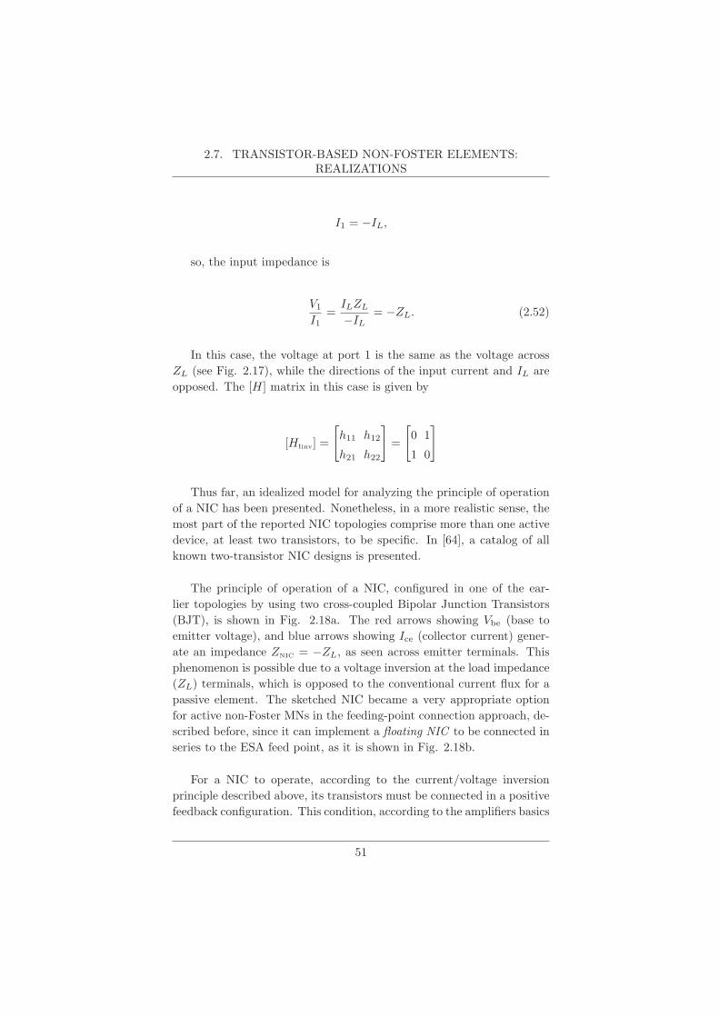
2.7. TRANSISTOR-BASED NON-FOSTER ELEMENTS:REALIZATIONS
I1 = −IL,
so, the input impedance is
V1
I1=
ILZL
−IL= −ZL. (2.52)
In this case, the voltage at port 1 is the same as the voltage across
ZL (see Fig. 2.17), while the directions of the input current and IL are
opposed. The [H] matrix in this case is given by
[HIinv] =
[h11 h12
h21 h22
]=
[0 1
1 0
]
Thus far, an idealized model for analyzing the principle of operation
of a NIC has been presented. Nonetheless, in a more realistic sense, the
most part of the reported NIC topologies comprise more than one active
device, at least two transistors, to be specific. In [64], a catalog of all
known two-transistor NIC designs is presented.
The principle of operation of a NIC, configured in one of the ear-
lier topologies by using two cross-coupled Bipolar Junction Transistors
(BJT), is shown in Fig. 2.18a. The red arrows showing Vbe (base to
emitter voltage), and blue arrows showing Ice (collector current) gener-
ate an impedance ZNIC = −ZL, as seen across emitter terminals. This
phenomenon is possible due to a voltage inversion at the load impedance
(ZL) terminals, which is opposed to the conventional current flux for a
passive element. The sketched NIC became a very appropriate option
for active non-Foster MNs in the feeding-point connection approach, de-
scribed before, since it can implement a floating NIC to be connected in
series to the ESA feed point, as it is shown in Fig. 2.18b.
For a NIC to operate, according to the current/voltage inversion
principle described above, its transistors must be connected in a positive
feedback configuration. This condition, according to the amplifiers basics
51
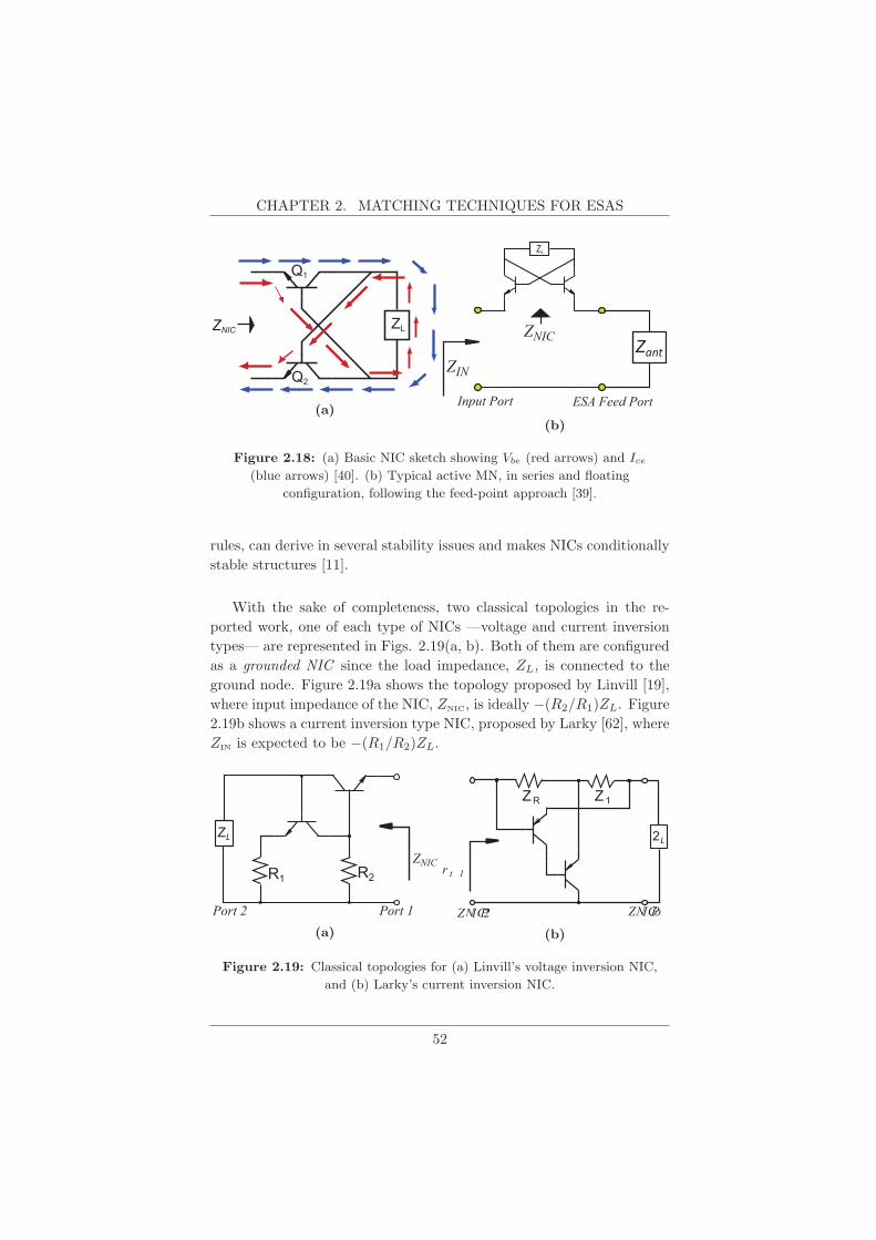
CHAPTER 2. MATCHING TECHNIQUES FOR ESAS
ZL
Q1
Q2
ZNIC
(a)
Zant
Input Port ESA Feed Port
ZIN
ZL
ZNIC
(b)
Figure 2.18: (a) Basic NIC sketch showing Vbe (red arrows) and Ice(blue arrows) [40]. (b) Typical active MN, in series and floating
configuration, following the feed-point approach [39].
rules, can derive in several stability issues and makes NICs conditionally
stable structures [11].
With the sake of completeness, two classical topologies in the re-
ported work, one of each type of NICs —voltage and current inversion
types— are represented in Figs. 2.19(a, b). Both of them are configured
as a grounded NIC since the load impedance, ZL, is connected to the
ground node. Figure 2.19a shows the topology proposed by Linvill [19],
where input impedance of the NIC, ZNIC, is ideally −(R2/R1)ZL. Figure
2.19b shows a current inversion type NIC, proposed by Larky [62], where
ZIN is expected to be −(R1/R2)ZL.
ZL
ZNICR1 R2
Port 1Port 2(a)
ZNICPo
r t 1
ZNICP2
ZR Z1
2L
(b)
Figure 2.19: Classical topologies for (a) Linvill’s voltage inversion NIC,
and (b) Larky’s current inversion NIC.
52
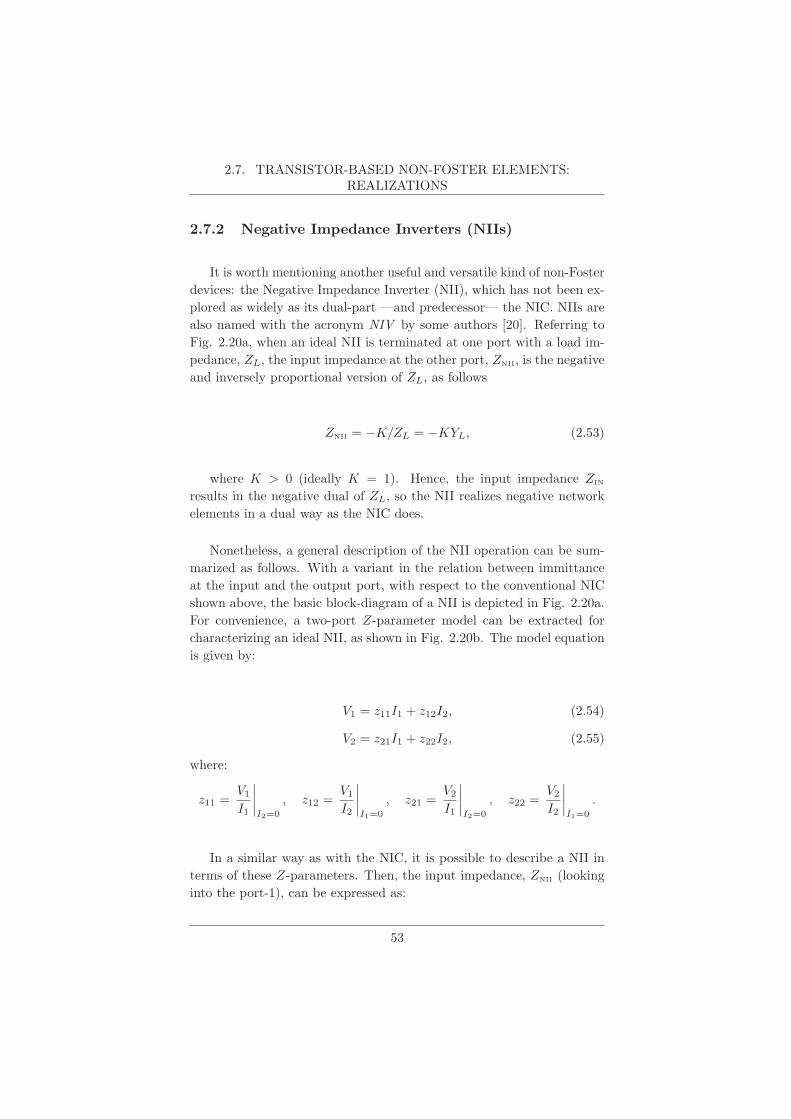
2.7. TRANSISTOR-BASED NON-FOSTER ELEMENTS:REALIZATIONS
2.7.2 Negative Impedance Inverters (NIIs)
It is worth mentioning another useful and versatile kind of non-Foster
devices: the Negative Impedance Inverter (NII), which has not been ex-
plored as widely as its dual-part —and predecessor— the NIC. NIIs are
also named with the acronym NIV by some authors [20]. Referring to
Fig. 2.20a, when an ideal NII is terminated at one port with a load im-
pedance, ZL, the input impedance at the other port, ZNII, is the negative
and inversely proportional version of ZL, as follows
ZNII = −K/ZL = −KYL, (2.53)
where K > 0 (ideally K = 1). Hence, the input impedance ZIN
results in the negative dual of ZL, so the NII realizes negative network
elements in a dual way as the NIC does.
Nonetheless, a general description of the NII operation can be sum-
marized as follows. With a variant in the relation between immittance
at the input and the output port, with respect to the conventional NIC
shown above, the basic block-diagram of a NII is depicted in Fig. 2.20a.
For convenience, a two-port Z-parameter model can be extracted for
characterizing an ideal NII, as shown in Fig. 2.20b. The model equation
is given by:
V1 = z11I1 + z12I2, (2.54)
V2 = z21I1 + z22I2, (2.55)
where:
z11 =V1
I1
∣∣∣∣I2=0
, z12 =V1
I2
∣∣∣∣I1=0
, z21 =V2
I1
∣∣∣∣I2=0
, z22 =V2
I2
∣∣∣∣I1=0
.
In a similar way as with the NIC, it is possible to describe a NII in
terms of these Z-parameters. Then, the input impedance, ZNII (looking
into the port-1), can be expressed as:
53
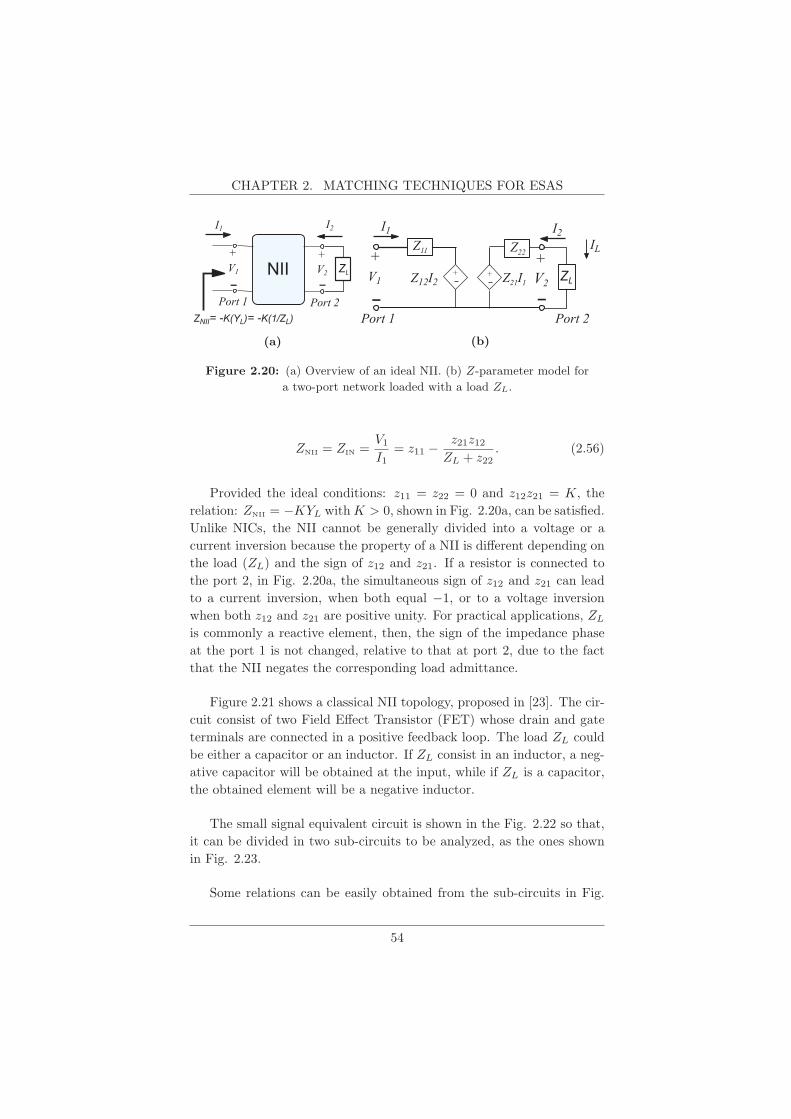
CHAPTER 2. MATCHING TECHNIQUES FOR ESAS
NII
I2
ZL
ZNII= -K(YL)= -K(1/ZL)
I1
V1 V2
+ +
Port 1 Port 2
(a)
ZLZ12I2 V2
+ +
Port 1 Port 2
+ Z21I1
Z11
V1
I1 I2IL
+
Z22
(b)
Figure 2.20: (a) Overview of an ideal NII. (b) Z-parameter model for
a two-port network loaded with a load ZL.
ZNII = ZIN =V1
I1= z11 − z21z12
ZL + z22. (2.56)
Provided the ideal conditions: z11 = z22 = 0 and z12z21 = K, the
relation: ZNII = −KYL withK > 0, shown in Fig. 2.20a, can be satisfied.
Unlike NICs, the NII cannot be generally divided into a voltage or a
current inversion because the property of a NII is different depending on
the load (ZL) and the sign of z12 and z21. If a resistor is connected to
the port 2, in Fig. 2.20a, the simultaneous sign of z12 and z21 can lead
to a current inversion, when both equal −1, or to a voltage inversion
when both z12 and z21 are positive unity. For practical applications, ZL
is commonly a reactive element, then, the sign of the impedance phase
at the port 1 is not changed, relative to that at port 2, due to the fact
that the NII negates the corresponding load admittance.
Figure 2.21 shows a classical NII topology, proposed in [23]. The cir-
cuit consist of two Field Effect Transistor (FET) whose drain and gate
terminals are connected in a positive feedback loop. The load ZL could
be either a capacitor or an inductor. If ZL consist in an inductor, a neg-
ative capacitor will be obtained at the input, while if ZL is a capacitor,
the obtained element will be a negative inductor.
The small signal equivalent circuit is shown in the Fig. 2.22 so that,
it can be divided in two sub-circuits to be analyzed, as the ones shown
in Fig. 2.23.
Some relations can be easily obtained from the sub-circuits in Fig.
54
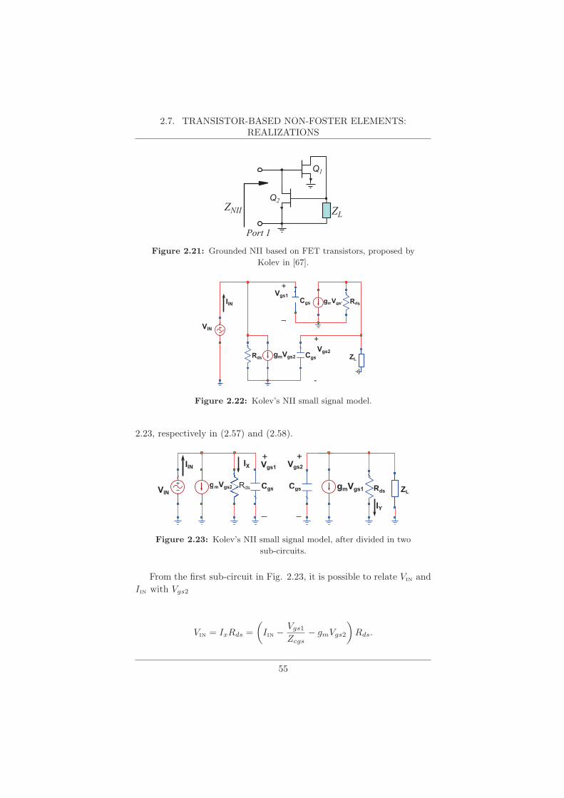
2.7. TRANSISTOR-BASED NON-FOSTER ELEMENTS:REALIZATIONS
ZNII
Port 1
ZL
Q1
Q2
Figure 2.21: Grounded NII based on FET transistors, proposed by
Kolev in [67].
VIN
gmVgs2Vgs2
+
-
Cgs
Vgs1Cgs
+
gmVgs1
Rds
RdsIIN
ZL
Figure 2.22: Kolev’s NII small signal model.
2.23, respectively in (2.57) and (2.58).
VIN gmVgs1
Vgs2Vgs1
Cgs
+
gmVgs2 Rds Rds
IIN
ZLCgs
IY
IX+
Figure 2.23: Kolev’s NII small signal model, after divided in two
sub-circuits.
From the first sub-circuit in Fig. 2.23, it is possible to relate VIN and
IIN with Vgs2
VIN = IxRds =
(IIN − Vgs1
Zcgs− gmVgs2
)Rds.
55

CHAPTER 2. MATCHING TECHNIQUES FOR ESAS
Assuming Vgs1 = VT, in some point in the active region of the FET,
then
VIN =
(IIN − VT
Zcgs− gmVgs2
)Rds. (2.57)
From the second sub-circuit in Fig. 2.23,
Vgs2 = IyRds =
(−Vgs2
Zcgs− gmVgs1 − Vgs2
ZL
)Rds
→ Vgs2
(1 +
Rds
Zcgs+
Rds
ZL
)= −gmVINRds,
thenVgs2
VIN
=−gmRds(
1 + Rds
Zcgs+ Rds
ZL
) . (2.58)
Now, combining (2.57) and (2.58)
VIN = IINRds − VINRds
Zcgs+
(gmRds)2(
1 + Rds
Zcgs+ Rds
ZL
)VIN
VIN
(1 +
Rds
Zcgs− (gmRds)
2
1 + Rds
Zcgs+ Rds
ZL
)= IINRds. (2.59)
Finally, the obtained input impedance is:
ZNII =VIN
IIN
=Rds
1 + Rds
ZCS− (gmRds)
2(1 + Rds
Zcgs+ Rds
ZL
)=
1
1Rds
+ 1Zcgs
+1
−1Rdsg2
m+ −1
Zcgsg2m
+ −1ZLg2
m
.
(2.60)
56

2.7. TRANSISTOR-BASED NON-FOSTER ELEMENTS:REALIZATIONS
Depending on the nature of ZL, either a negative inductor or negative
capacitor can be obtained. If ZL = jωL, ZNII behaves as the circuit in
Fig. 2.24, and can be computed as (2.61).
gs
Cn
Rds
LnRn
ZNII
Figure 2.24: Equivalent input impedance of the Kolev’s NII model,
when ZL is an inductor.
ZNII =1
1Rds
+ 1Zcgs
+1
−1Rdsg2
m+ −1
g2m(jωCgs) +
−1jωLg2
m
, (2.61)
where
Rn = − 1
g2mRds; Ln =
−Cgs
g2m; Cn = −g2mL. (2.62)
So, the total input impedance can be modeled as
ZNII = − 1
Rdsg2m− jω
Cgs
g2m− 1
jωLg2m. (2.63)
If the FET is carefully selected, the effect of Cgs and Rds can be neg-
ligible (at least at low frequencies), and the circuit will work as a series
combination of a negative capacitor, proportional to the load inductor L,
with a parasitic negative inductor and resistor. These last ones should
be compensated with a corresponding series resistor and inductor at the
input.
In that way, the response over the operation frequency interval can
be approximated as
57
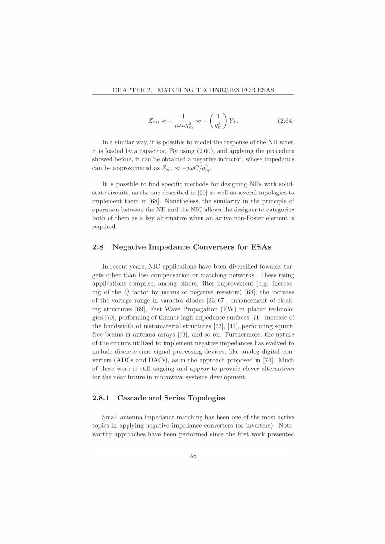
CHAPTER 2. MATCHING TECHNIQUES FOR ESAS
ZNII ≈ − 1
jωLg2m≈ −(
1
g2m
)YL. (2.64)
In a similar way, it is possible to model the response of the NII when
it is loaded by a capacitor. By using (2.60), and applying the procedure
showed before, it can be obtained a negative inductor, whose impedance
can be approximated as ZNII ≈ −jωC/g2m.
It is possible to find specific methods for designing NIIs with solid-
state circuits, as the one described in [20] as well as several topologies to
implement them in [68]. Nonetheless, the similarity in the principle of
operation between the NII and the NIC allows the designer to categorize
both of them as a key alternative when an active non-Foster element is
required.
2.8 Negative Impedance Converters for ESAs
In recent years, NIC applications have been diversified towards tar-
gets other than loss compensation or matching networks. These rising
applications comprise, among others, filter improvement (e.g. increas-
ing of the Q factor by means of negative resistors) [64], the increase
of the voltage range in varactor diodes [23, 67], enhancement of cloak-
ing structures [69], Fast Wave Propagation (FW) in planar technolo-
gies [70], performing of thinner high-impedance surfaces [71], increase of
the bandwidth of metamaterial structures [72], [44], performing squint-
free beams in antenna arrays [73], and so on. Furthermore, the nature
of the circuits utilized to implement negative impedances has evolved to
include discrete-time signal processing devices, like analog-digital con-
verters (ADCs and DACs), as in the approach proposed in [74]. Much
of these work is still ongoing and appear to provide clever alternatives
for the near future in microwave systems development.
2.8.1 Cascade and Series Topologies
Small antenna impedance matching has been one of the most active
topics in applying negative impedance converters (or inverters). Note-
worthy approaches have been performed since the first work presented
58
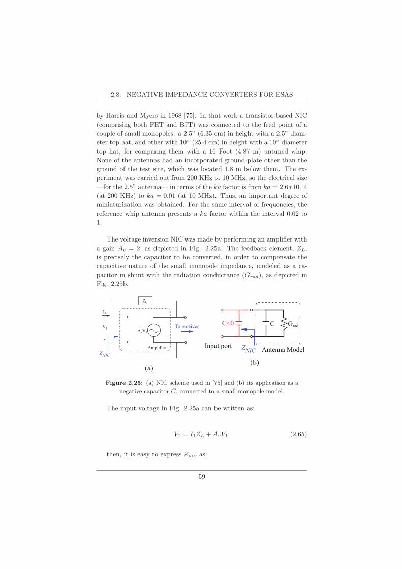
2.8. NEGATIVE IMPEDANCE CONVERTERS FOR ESAS
by Harris and Myers in 1968 [75]. In that work a transistor-based NIC
(comprising both FET and BJT) was connected to the feed point of a
couple of small monopoles: a 2.5” (6.35 cm) in height with a 2.5” diam-
eter top hat, and other with 10” (25.4 cm) in height with a 10” diameter
top hat, for comparing them with a 16 Foot (4.87 m) untuned whip.
None of the antennas had an incorporated ground-plate other than the
ground of the test site, which was located 1.8 m below them. The ex-
periment was carried out from 200 KHz to 10 MHz, so the electrical size
—for the 2.5” antenna— in terms of the ka factor is from ka = 2.6∗10−4(at 200 KHz) to ka = 0.01 (at 10 MHz). Thus, an important degree of
miniaturization was obtained. For the same interval of frequencies, the
reference whip antenna presents a ka factor within the interval 0.02 to
1.
The voltage inversion NIC was made by performing an amplifier with
a gain Av = 2, as depicted in Fig. 2.25a. The feedback element, ZL,
is precisely the capacitor to be converted, in order to compensate the
capacitive nature of the small monopole impedance, modeled as a ca-
pacitor in shunt with the radiation conductance (Grad), as depicted in
Fig. 2.25b.
Amplifier
I1
+
-
V1 AvV1
ZL
ZNIC
To receiver
(a)
GradC
Input port
C<0
ZNIC Antenna Model
(b)
Figure 2.25: (a) NIC scheme used in [75] and (b) its application as a
negative capacitor C, connected to a small monopole model.
The input voltage in Fig. 2.25a can be written as:
V1 = I1ZL +AvV1, (2.65)
then, it is easy to express ZNIC as:
59
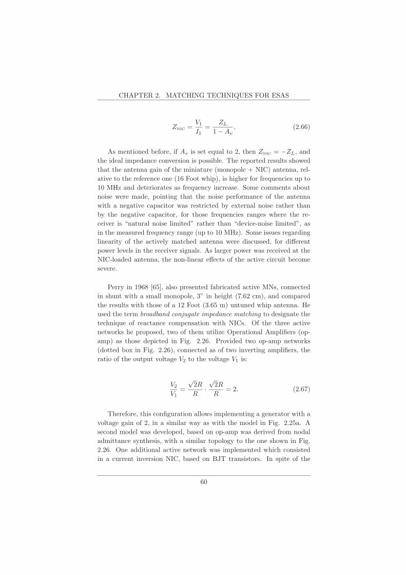
CHAPTER 2. MATCHING TECHNIQUES FOR ESAS
ZNIC =V1
I1=
ZL
1−Av. (2.66)
As mentioned before, if Av is set equal to 2, then ZNIC = −ZL, and
the ideal impedance conversion is possible. The reported results showed
that the antenna gain of the miniature (monopole + NIC) antenna, rel-
ative to the reference one (16 Foot whip), is higher for frequencies up to
10 MHz and deteriorates as frequency increase. Some comments about
noise were made, pointing that the noise performance of the antenna
with a negative capacitor was restricted by external noise rather than
by the negative capacitor, for those frequencies ranges where the re-
ceiver is “natural noise limited” rather than “device-noise limited”, as
in the measured frequency range (up to 10 MHz). Some issues regarding
linearity of the actively matched antenna were discussed, for different
power levels in the receiver signals. As larger power was received at the
NIC-loaded antenna, the non-linear effects of the active circuit become
severe.
Perry in 1968 [65], also presented fabricated active MNs, connected
in shunt with a small monopole, 3” in height (7.62 cm), and compared
the results with those of a 12 Foot (3.65 m) untuned whip antenna. He
used the term broadband conjugate impedance matching to designate the
technique of reactance compensation with NICs. Of the three active
networks he proposed, two of them utilize Operational Amplifiers (op-
amp) as those depicted in Fig. 2.26. Provided two op-amp networks
(dotted box in Fig. 2.26), connected as of two inverting amplifiers, the
ratio of the output voltage V2 to the voltage V1 is:
V2
V1=
√2R
R·√2R
R= 2. (2.67)
Therefore, this configuration allows implementing a generator with a
voltage gain of 2, in a similar way as with the model in Fig. 2.25a. A
second model was developed, based on op-amp was derived from nodal
admittance synthesis, with a similar topology to the one shown in Fig.
2.26. One additional active network was implemented which consisted
in a current inversion NIC, based on BJT transistors. In spite of the
60
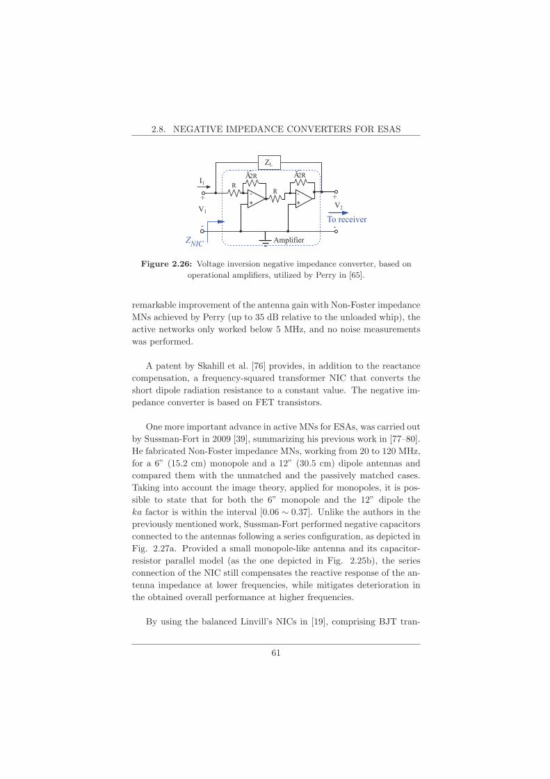
2.8. NEGATIVE IMPEDANCE CONVERTERS FOR ESAS
Amplifier
I1
+
-
V1V2
ZL
ZNIC
To receiver
+- +
-
R
+-R
Ā2R Ā2R
Figure 2.26: Voltage inversion negative impedance converter, based on
operational amplifiers, utilized by Perry in [65].
remarkable improvement of the antenna gain with Non-Foster impedance
MNs achieved by Perry (up to 35 dB relative to the unloaded whip), the
active networks only worked below 5 MHz, and no noise measurements
was performed.
A patent by Skahill et al. [76] provides, in addition to the reactance
compensation, a frequency-squared transformer NIC that converts the
short dipole radiation resistance to a constant value. The negative im-
pedance converter is based on FET transistors.
One more important advance in active MNs for ESAs, was carried out
by Sussman-Fort in 2009 [39], summarizing his previous work in [77–80].
He fabricated Non-Foster impedance MNs, working from 20 to 120 MHz,
for a 6” (15.2 cm) monopole and a 12” (30.5 cm) dipole antennas and
compared them with the unmatched and the passively matched cases.
Taking into account the image theory, applied for monopoles, it is pos-
sible to state that for both the 6” monopole and the 12” dipole the
ka factor is within the interval [0.06 ∼ 0.37]. Unlike the authors in the
previously mentioned work, Sussman-Fort performed negative capacitors
connected to the antennas following a series configuration, as depicted in
Fig. 2.27a. Provided a small monopole-like antenna and its capacitor-
resistor parallel model (as the one depicted in Fig. 2.25b), the series
connection of the NIC still compensates the reactive response of the an-
tenna impedance at lower frequencies, while mitigates deterioration in
the obtained overall performance at higher frequencies.
By using the balanced Linvill’s NICs in [19], comprising BJT tran-
61
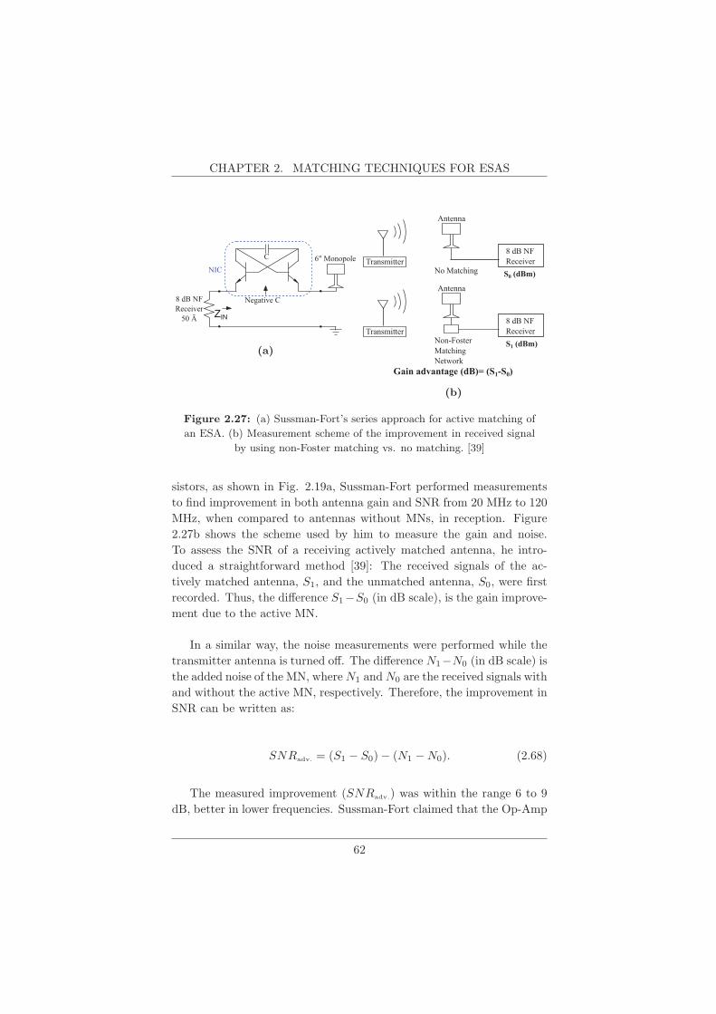
CHAPTER 2. MATCHING TECHNIQUES FOR ESAS
Negative C
ZIN
6" Monopole
8 dB NFReceiver
50 Ā
C
NIC
(a)
Gain advantage (dB)= (S1-S0)
Transmitter
Antenna
Non-FosterMatching Network
8 dB NFReceiver
Transmitter
Antenna
No Matching
8 dB NFReceiverS0 (dBm)
S1 (dBm)
(b)
Figure 2.27: (a) Sussman-Fort’s series approach for active matching of
an ESA. (b) Measurement scheme of the improvement in received signal
by using non-Foster matching vs. no matching. [39]
sistors, as shown in Fig. 2.19a, Sussman-Fort performed measurements
to find improvement in both antenna gain and SNR from 20 MHz to 120
MHz, when compared to antennas without MNs, in reception. Figure
2.27b shows the scheme used by him to measure the gain and noise.
To assess the SNR of a receiving actively matched antenna, he intro-
duced a straightforward method [39]: The received signals of the ac-
tively matched antenna, S1, and the unmatched antenna, S0, were first
recorded. Thus, the difference S1−S0 (in dB scale), is the gain improve-
ment due to the active MN.
In a similar way, the noise measurements were performed while the
transmitter antenna is turned off. The difference N1−N0 (in dB scale) is
the added noise of the MN, whereN1 andN0 are the received signals with
and without the active MN, respectively. Therefore, the improvement in
SNR can be written as:
SNRadv. = (S1 − S0)− (N1 −N0). (2.68)
The measured improvement (SNRadv.) was within the range 6 to 9
dB, better in lower frequencies. Sussman-Fort claimed that the Op-Amp
62
2.8. NEGATIVE IMPEDANCE CONVERTERS FOR ESAS
alternative to implement non-Foster MN, in the same small monopole,
resulted in at least 10 dB more generated noise due to the NIC than
with the BJT-based topology. In [80], the highest effective frequency
range obtained by means of the active MN, to a 20” x 2” lossy dipole
antenna, is from 60 MHz to 400 MHz. It is also shown an antenna gain
improvement.
Additionally, his earlier work [77], [81] laid the foundation for non-
Foster transmitting matching networks. Besides the design of circuits
delivering a few milliwatts to an ESA, were developed both class A-
and class B-biased NICs which included a strategy for tackling the high-
voltage problem, inherent to transmitting mode in active loaded ESAs.
In this sense, it was suggested that a negative LC matching could be
applied to an electrically small antenna to mitigate that problem. It was
shown that the resonance of the antenna caused by the negative LC net-
work forces to transfer the maximum power to the antenna (for a narrow
bandwidth). He also pointed out that the power efficiency —including
Direct Current (DC) biasing for transistors— should be taken into ac-
count in applications of Non-Foster matching for transmitting antennas.
With this idea, class C-biased NICs in [39] were introduced to improve
the power efficiency of transmitting antennas, achieving a factor-of-two
improvement in power efficiency over the best passive match to an ESA
model (at 20 MHz). Across 5% bandwidth, an average signal power of
over 1 W can be delivered to the radiation resistance. In spite of the fact
that nor the linearity of the active circuits, neither the stability analysis
for the prototyped designs were presented in his papers, Sussman-Fort
made remarkable contributions to the field of active MN applied to elec-
trically small antennas.
Following the aforementioned results, other authors in [41], [82] and
[83] presented active and transistor-based matching networks, connected
to the driven point of some canonical small antenna structures (e.g. small
monopoles or loops). The effort in these work was mostly focused on the
implementation of a stable and fully characterized active MN, more than
in studying the performance of the whole antenna system (antenna plus
NIC). It is possible to conclude that unavoidable issues arise from the
parasitics well in the selected active devices well in the manufacturing
technology.
63
CHAPTER 2. MATCHING TECHNIQUES FOR ESAS
Another worthy contribution to mention was made by O. Tade et
al. in 2012 [45], in which an active non-Foster MN was performed and
measured, and then, applied to the driving point of a chassis antenna
with a base of 50 mm X 50 mm. A customized stability analysis tech-
nique was developed and applied to show how to design a NIC for stable
operation at frequencies up to 1.5 GHz, using the BFS-17 BJT transis-
tor. Acceptable matching results were reported for the 595 MHz to 1.5
GHz band. It is important to note that the upper bound of operation
for the active MN presented by Tade reached 1.5 GHz, unlike all the
NIC-based MNs showed thus far, reported to work up to 200 MHz. One
possible reason can be the symmetry in the component placing and the
carefully designed feedback paths as well as the feed lines used to couple
the measured signal.
Linearity measurements were also conducted by Tade, by means of
the third order intermodulation product (OIP3) [45], resulting in a mea-
sured OIP3 comparable with other typical front-end components using
similar transistors. A SNR advantage (SNRadv.) between 2 dB and 12
dB compared to the resistively equalized passive antenna was also re-
ported. However, because of a disruption on the antenna ground plane
(where the active MN is placed) that disturbs the surface current and
causes the antenna impedance to change, neither the noise analysis nor
the linearity analysis could be undertaken in the proposed antenna. In-
stead, an additional NIC connected to an equivalent passive circuit, de-
signed to generate the same antenna impedance, was studied. This fact
made impractical the initially proposed structure for carrying out the
whole antenna performance analysis.
2.8.2 Embedded non-Foster Matching Networks
Subsequently, additional work has been developed and implemented
by other authors in the past few years, including clever approaches in
sophisticated antenna structures. One of these approaches consists in
embedding a non-Foster element into a resonant antenna [38,42,44,84].
These antennas try to eliminate the external MN by substituting the
external circuit with an internal one, intrinsically matched to a particular
antenna providing a reasonable radiation resistance.
Two different strategies have been followed in this line. The first one
64

2.8. NEGATIVE IMPEDANCE CONVERTERS FOR ESAS
consists on including the non-Foster network inside the antenna itself to
obtain a broadband matched antenna. A re-shaping of the current distri-
butions over the antenna structure takes place, as in the work proposed
by Mirzaei and Eleftheriades in [42]. Their strategy included a printed
and slotted monopole, like the one depicted in Fig. 2.14b, in which the
tunability was first checked by means of a variable capacitor —a varac-
tor diode— leading to the synthesis of a non-Foster circuit, needed to
obtain broadband matching.
The second one consists on putting the non-Foster network in a para-
sitic element, that modifies the antenna near-field components, inspired
in a metamaterial structure, like the model proposed by Barbuto et al.
in [44]. In this sense, other work has been developed by loading a Near-
Field Resonant Parasitic (NFRP) with a non-Foster form, as Zhu and
Ziolkowski describe in [38] and [84]. In all these works, the design pro-
cedure departs from a metamaterial-inspired antenna, followed by the
inclusion of a variable reactance (i.e. conventional capacitance or in-
ductance) in order to verify the frequency-agility (or tunability) of the
antenna, as mentioned in previous sections. From the frequency-agile
antenna, the needed reactance can be fulfilled by the inclusion of a non-
Foster MN.
The embedded active MN approach is the one selected to be devel-
oped along this work. The fact that the active MN is embedded into
the antenna structure allow the designer to use the NIC-loaded ESA in
both receiving and transmitting modes, provided the consideration of
the high voltage condition in transmitting mode, as mentioned before.
Additionally, it is very important to note that in none of the reported
work, where the embedded MN approach was applied, the possibility of
exploring the effect of changing the NFC location has been observed.
This exploration leads to additional considerations which are part of
a complete design strategy for ESAs, actively loaded with non-Foster
elements, that will be developed across the subsequent chapters.
65


CHAPTER 3
EMBEDDED NON-FOSTER MATCHINGNETWORKS FOR ESAS
3.1 Introduction
In the previous chapter, the basic idea of active matching for elec-
trically small antennas (ESAs) was described. Thus, by means of the
inclusion —or the connection at the feed point— of a non-Foster net-
work, it is possible to achieve broader bandwidths at lower frequencies,
compared to the counterpart: the passive lumped matching networks
(MNs). It was also shown how active-matching technique has become
a very active topic during the last years. Since the passive matching
approach in ESAs is strongly limited by the gain-bandwidth constraint
— the Bode [11], Fano [12] and Youla [16] criterion— and also by the
maximum achievable bandwidth constraint for small-sized antennas —
imposed byWheeler [10], Chu [13] and Thal [17] criteria— all the authors
have taken advantage of the reactance properties in non-Foster elements
to neutralize the ESA reactance.
In particular, as mentioned earlier, the negative-slope property of
the reactance response in non-Foster circuits (NFCs) has been used to
emulate the resonance condition in the antenna, not only at one single
frequency but over larger bandwidths. In this sense, all the reported

CHAPTER 3. PARAMETER SENS
work so far has taken the assumption of a fixed and predictable charac-
teristic of the ESA impedance: its larger reactance and its small resistive
part. Additionally, most of the effort has been targeted to design a prop-
erly performed NIC to be connected at the feed point of the antenna,
without paying any special attention to the location of such active non-
Foster network. Even in the cases where a NIC circuit is placed inside
the antenna structure, the reported work does not take in mind any
consideration about the best possible location for the intended active
MN.
Some analytical exploration was carried out by the author, regarding
the influence on the needed impedance —to be fulfilled through the ac-
tive MN— that is produced by changing the location of such active MN,
within the antenna structure itself. These explorations derived in finding
two crucial parameters related to the non-Foster MN location. First, the
sensitivity of the obtained impedance matching —at the antenna input
port— due to the difference between the analytical impedance and the
one implemented through the non-Foster MN. Second, the realizability
of the needed analytical impedance at that point, in terms of quantity
of non-Foster elements and its values, to obtain the intended broadband
impedance matching.
The two-port antenna approach, first proposed by Koulouridis in [85]
and [86], has demonstrated to be a suitable starting point in the strategy
to obtain the aforementioned parameters — the sensitivity to the MN
location, and the analytical non-Foster impedance— at a certain point.
The two-port antenna approach consists of including an additional —
and fictitious— port inside the antenna, by means of a Computer-Aided
Design (CAD) software suite for full-wave simulation. The idea is to
extract some two-port network parameters, for example, the S- or the
ABCD-parameters matrices. Once the network parameters have been
extracted for each two-port combination, according to the number of
locations to be analyzed, the analytical procedure takes place. The ori-
entation of the analysis is to control, in somehow, the internal impedance
of the network, which is an indicator of how difficult —or even possible—
the active impedance matching is going to be. The detailed method will
be shown in the subsequent sections.
In other words, the present chapter aims at explaining and analyt-
68

3.2. TWO-PORT ANTENNA APPROACH FOR ACTIVEIMPEDANCE MATCHING
ically finding a suitable location for the active non-Foster MN into the
antenna, by means of the two-port antenna approach. In addition, a
one-port antenna using internal MN can also be considered as two-port
antenna, where the second port represents the non-Foster circuit. The
effects on the antenna performance when changing the position of the
NFC, are also investigated. The author introduces a sensitivity parame-
ter in this chapter, which shows the effect on the matched antenna input
impedance, associated with the variations of the loading non-Foster im-
pedance. This new parameter has been shown to be critical during the
design procedure. Finally, alongside the sensitivity analysis, the type of
non-Foster form is also analyzed to take into account the efficiency, and
its effect on the radiation pattern.
3.2 Two-Port Antenna Approach for Active Impe-
dance Matching
Treating an antenna as a multiport network is an interesting ap-
proach based on simple circuit theory principles [86]. By adding one or
more ports to the antenna structure is possible to obtain a multiport
microwave device in which one of the ports corresponds to the initial
feeding port. Surely, the original input impedance —at the input port—
is reproduced by letting all the added ports open circuited. It is possible
to relate the antenna impedance, Zant, with the impedance connected at
the fictitious port, ZP2, through the extracted network parameters ([S]
or [ABCD]), as it is shown in Fig. 3.1.
The initial idea tried to internally increase the real part of the an-
tenna impedance to reach, ideally, the system reference value (Z0). To do
so, Koulouridis proposed the use of passive-lumped or possibly negative
elements (NFCs). Then, a series non-Foster network is connected out-
side the antenna, for compensating the remaining antenna’s reactance.
Nonetheless, no especial attention is paid to the location of the added
port-2, and no considerations are given to the possible changes that can
occur in the input impedance due to possible changes in such port-2
location either.
Now, as mentioned before, the two-port antenna approach is applied
to the active non-Foster matching strategy, presented in this work. The
69

CHAPTER 3. PARAMETER SENS
Two-port Antenna
ZA ZIN
Antenna Insertion of a second port
Analysis/simulationof the antenna
Extraction of the S-/ABCD-parameters
ZIN
P1 P1
P2
ZP2
(Antenna) (Antenna)
(a)
(b)
(Antennafeed point)
AZP2+B CZP2+DZIN=
DZIN-B CZIN-A
ZP2=-
S- or ABCD-parameters
P1 P2Antenna Antenna
Figure 3.1: (a) Block diagram explaining the two-port antenna
approach. (b) The relation between ZIN and ZL through the
ABCD-parameters [86].
basic scheme of the active matching for two-port antennas is shown in
Fig. 3.2. It consists of loading the introduced analytical port-2 of the
antenna with a non-Foster impedance, ZNIC (implemented by the use
of a NIC), in such a way that the input impedance at the other port
equals some reference value, Z0. To introduce the fictitious port —
generally called lumped port or discrete port in most electromagnetic
CAD simulators— can be added inside the antenna 3D-model. The
added excitation can be connected in both a grounded or a floating
configuration, according to the nature of the radiating element or some
constraints imposed by the application. This procedure is described in
more detail throughout the design examples.
It is worth noting that there is no need for a lumped-elements model
of the antenna, difficult to extract in practice. The S-parameter matrix
can be easily obtained by modeling the structure in an electromagnetic
CAD software. This fact facilitates and generalizes the design process
to a massive variety of antenna types while takes advantage from the
increasing computational power of the actual Personal Computers (PC),
and High-Performance Computing (HPC) servers.
The input impedance, ZIN, in Fig. 3.2 is
ZIN = Z01 + ΓIN
1− ΓIN
. (3.1)
70

3.2. TWO-PORT ANTENNA APPROACH FOR ACTIVEIMPEDANCE MATCHING
Figure 3.2: Active Matching of Two-Port Antenna.
Then, the reflection coefficient of this loaded two-port network at its
input, ΓIN, is given by
ΓIN = S11 +S12 · S21 · ΓNIC
1− S22 · ΓNIC
. (3.2)
Since the goal is to have a matched antenna over a desired bandwidth
(theoretically it could be at all the frequencies), the input reflection coef-
ficient should be zero along this bandwidth. After some straightforward
calculations and equating (3.2) to zero, we can obtain the optimum and
analytical reflection coefficient that the non-Foster network should pro-
vide, ΓanNIC, as in (3.3). The superscript “an” stands for analytical and
represents the ideal value or condition that should be meet to obtain the
ideal result in the parameter under design.
ΓanNIC =
S11
S22 · S11 − S12 · S21. (3.3)
Therefore, the non-Foster analytic impedance, ZanNIC, which is related
with the reflection coefficient, ΓanNIC , is given by
ZanNIC = Z0
(1 + ΓanNIC)
(1− ΓanNIC)
, (3.4)
and can also be expressed in terms of the two-port S-parameters of
the antenna as:
71
CHAPTER 3. PARAMETER SENS
ZanNIC = Z0 ·
(S22 · S11 − S12 · S21 + S11
S22 · S11 − S12 · S21 − S11
). (3.5)
When this analytical impedance ZanNIC is placed at port-2, the reflec-
tion coefficient at port-1, ΓIN, would ideally equal 0 at all frequencies
and, hence, large bandwidths can be obtained.
In this point, it is important to note the dependence of ZanNIC on the
extracted S-parameters, and therefore on frequency as the [S] matrix is
also a function of frequency. This condition implies a dependence of the
input impedance, ZIN, on the S-parameters. This last dependence can
be deduced by the relation of ZIN with ΓIN in (3.1), then, in the relation
between ΓIN and ΓNIC through (3.2), and finally in the expression of ZanNIC
in (3.5), in terms of the S-parameters only, which aims at meeting the
goal ΓIN = 0.
In other words, ZIN is directly related to ZNIC, but this relation can
only be observed through the S-parameters calculation —or other net-
work parameters— when the non-Foster matching for two-port antenna
approach is used. The role of ZanNIC is to assure the matching condi-
tion over the intended frequency band, according to the mathematical
reasoning shown so far. Thus, the implementation of ZanNIC with real cir-
cuits is a key factor in this strategy, and some additional consideration
which allows us to observe the influence of the differences between the
analytical ZanNIC and a real NIC impedance is welcome.
3.3 The Sensitivity Parameter Sens: Definition
Till now, it has been shown how a zero reflection coefficient at the
input port is possible by calculating the impedance ZanNIC, needed at port-
2, only by means of the S-parameters of a simple two-port network.
However, due to the fact that the NIC impedance is quite sensitive to
parasitics and variations on its load impedance (ZL in Fig. 3.2) [19], [87],
it is also very important to analyze how these changes affect to obtain
the goal. Then a new parameter, called Sens, can be defined such as the
sensitivity of this solution, which is given by
72

3.3. THE SENSITIVITY PARAMETER SENS : DEFINITION
ΔΓIN =∂ΓIN
∂ΓNIC
∣∣∣∣ΓNIC=Γan
NIC︸ ︷︷ ︸Sensitivity: Sens
·ΔΓNIC = Sens ·ΔΓNIC. (3.6)
This sensitivity parameter provides information about how poten-
tial variations in the impedance of the NIC (represented by ΓNIC) with
respect to the analytic one, given by (3.3), affect the input reflection
coefficient, ΓIN. In order to deduce the expression for Sens, we can apply
the quotient rule for derivatives in (3.2) as:
∂ΓIN
∂ΓNIC
=∂
∂ΓNIC
(S11 +
S12 · S21 · ΓNIC
1− S22 · ΓNIC
), (3.7)
that leads to
∂ΓIN
∂ΓNIC
=(1− S22ΓNIC)(S12S21)− (S12S21ΓNIC)(−S22)
(1− S22ΓNIC)2
=(S12S21)(1− S22ΓNIC + S22ΓNIC)
(1− S22ΓNIC)2
=S21S12
(1− S22ΓNIC)2 .
Then, if we evaluate the derivative for ΓNIC = ΓanNIC, and take the
absolute value:
Sens =
∣∣∣∣ ∂ΓIN
∂ΓNIC
∣∣∣∣∣∣∣∣ΓNIC=Γan
NIC
=
∣∣∣∣∣ S21S12
(1− S22ΓanNIC)
2
∣∣∣∣∣ . (3.8)
Now, by applying the expression in (3.3) into (3.8), the parameter
Sens can be obtained as follows
73

CHAPTER 3. PARAMETER SENS
Sens =
∣∣∣∣∣∣∣S12S21(
1− S11S22
S11S22−S12S21
)2∣∣∣∣∣∣∣
=
∣∣∣∣∣∣∣S12S21(−S12S21
S11S22−S12S21
)2∣∣∣∣∣∣∣
=
∣∣∣∣∣S12S21 (S11S22 − S12S21)2
(−S12S21)2
∣∣∣∣∣ .
Finally:
Sens =
∣∣∣∣∣ (S11S22 − S12S21)2
S12S21
∣∣∣∣∣ . (3.9)
As in the case of ZanNIC, this last expression for Sens depends on the
S-parameters, and therefore, on frequency also. Thus, it is possible to
observe how difficult is to match the ESA —or any other antenna— all
along the frequency interval of design.
If the two ports are symmetrically placed (S11= S22 and S12= S21),
equation (3.9) can be rewritten as:
Sens =
∣∣∣∣∣(S11
2 − S212)2
S212
∣∣∣∣∣ =∣∣∣∣∣ ((S11+S21) · (S11 − S21))
2
S212
∣∣∣∣∣ . (3.10)
In the symmetric case the sensitivity still depends on the S -
parameters of the two-port antenna only. The two ports must be placed
in such a way that the sensitivity is minimized. Otherwise, any small
change in the impedance, provided by the NIC, will dramatically affect
the antenna performance in terms of the impedance bandwidth.
The Sens parameter is an indicator of how the difference between the
actual ZNIC —from a real NFC— and the ideal one, ZanNIC —computed
74

3.3. THE SENSITIVITY PARAMETER SENS : DEFINITION
as (3.5)— actually influences the input impedance: ZIN. Thus, Sens
should be computed at every single point where port-2 is placed into
the antenna. At each port-2 location, calculation of Sens describes such
influence all along the frequency interval from which the S-parameters
have been extracted. In this sense, according to the designs carried out
by the author, which will be shown later, a Sens lower than 10 dB is con-
sidered as a reasonable value to obtain an impedance bandwidth wide
enough to be implemented with an active MN. SensdB is calculated as
20 log(|Sens|) where |Sens| is given by (3.9) or (3.10), and for simplicity,
in this work it will be referred as Sens. Therefore, once Sens is calcu-
lated at different points over the antenna structure, those at which Sens
is lower than 10 dB can be considered as appropriate to place the active
MN. Those low-sensitivity points represent robustness against the inher-
ent changes and deviations proper of the implementation of ZanNIC with
active devices.
From the previous expressions, it can also be concluded that the
sensitivity will be smaller when the transmission parameter (S21) equals,
in magnitude, the reflection parameter (S11). This provides an idea
about what kind of antennas are more suitable to be used in non-Foster
active matching designs, as it will be shown below. The Sens parameter
will be approximately flat for non-resonant antennas while will present
different magnitude peaks for resonant ones. In general, very resonant
antennas will present higher values of Sens, and hence, will be harder to
match along a broad bandwidth since S21 is very small and would only
agree with the S11 across very small frequency bands. Then, if high levels
of coupling can be engineered for a high-Q two-port antenna (or even a
multiport one), the return and insertion losses can be similar over larger
bandwidths, and the sensitivity can be kept low over those bandwidths,
enabling a broadband active matching design. In other words, if S21 is
low, in comparison with S11, the non-Foster element connected to port-
2 has not much influence on the port-1. Other way, in terms of the
antenna size, when it decreases in electrical terms (i.e. in an ESA), the
quality factor Q of the antenna increases dramatically, as it was shown
in previous sections. However, we could find a low sensitivity point over
its structure, so a broadband active matched antenna design would be
feasible, as we will see below devoted to a loop antenna.
75

CHAPTER 3. PARAMETER SENS
3.4 The Sens parameter and the Bandwidth
In a similar way, as for the input reflection coefficient ΓIN in the two-
port antenna model, it is possible to relate the Sens parameter in (3.9)
with changes in the resulting impedance (or VSWR) bandwidth.
So, we can obtain a minimum allowable value for the magnitude of
ΓIN in (3.11); (e.g. |ΓIN min| = 0.316 for the typical |S11| = −10 dB) and
relates its changes with the changes in VSWR.
V SWRmax =1 + |ΓIN min|1− |ΓIN min| . (3.11)
The Impedance Bandwidth related to a certain VSWR (BWv), ob-
tained at the input (port-1 in Fig.3.2), can be defined as the frequency
interval, around a frequency ω0, at which the VSWR equals a maximum
bound (e.g. V SWRmax = 1.92 for |S11| = −10 dB) [88]. BWv is one
of the most relevant properties to describe the performance of an ESA
after a MN —active of passive— is added, and also used to compare
the results between different designs. Thus, BWv can be computed as a
function of VSWR, as follows:
BWV ≈ 2 · ω0 (V SWRmax − 1)
Q · √V SWRmax
. (3.12)
In [89], expressions similar to (3.12) are derived for planar antennas
with linear and circular polarizations.
Hence, by applying the chain rule for derivatives, an expression re-
lating BWv with the Sens parameter and with the changes in the ΓNIC
can be devised utilizing (3.2), (3.11), and (3.12), under the assumption
that |ΓIN| must equal zero. Moreover, for the following expressions, a
tuned ESA is assumed to work around a frequency ω0, which is far away
from the natural antiresonant frequency, associated with the radiating
structure itself, according to the work presented in [88].
76

3.4. THE SENS PARAMETER AND THE BANDWIDTH
First, taking the derivative of (3.2) with respect to ΓNIC, and evalu-
ating it at ΓNIC = ΓanNIC, results in the expression shown before as Sens,
in (3.9), modified here as
∣∣∣∣ ∂ΓIN
∂ΓNIC
∣∣∣∣∣∣∣∣ΓNIC=Γan
NIC
= Sens
→ ΔΓIN = Sens ·ΔΓNIC.
(3.13)
Second, by taking the derivative in (3.11) with respect to the magni-
tude of ΓIN, and evaluating it at zero (|ΓIN| = 0), provided the condition
ΓNIC = ΓanNIC, an expression arises as follows
∂V SWR
∂|ΓIN|∣∣∣∣|ΓIN|=0
ΓNIC=ΓanNIC
=(1− |ΓIN|) + (1 + |ΓIN|)
1− 2|ΓIN|+ |ΓIN|2∣∣∣∣|ΓIN|=0
= 2. (3.14)
Third, by taking the derivative in (3.12) with respect to VSWR,
and evaluating it at V SWR = V SWRmax = 1 —the ideal condition,
consequence of connecting ΓanNIC at port-2— an expression arises as follows
(for briefness in the expression, the variable V SWRmax is replaced by s,
as in [88])
∂BWV
∂V SWRmax
∣∣∣∣V SWRmax=s=1
|ΓIN|=0
ΓNIC=ΓanNIC
=2ω0
Q
[√s− s−1
2√s
s
]∣∣∣∣∣s=1
=2ω0(s+ 1)
Qs3/2
∣∣∣∣s=1
=4ω0
Q.
(3.15)
Finally, by applying the chain rule for derivatives, and using (3.13),
(3.14), and (3.15), the complete expression to relate changes in BWV
with respect to those in ΓNIC can be given as follows
77
CHAPTER 3. PARAMETER SENS
∂BW V
∂ΓNIC
∣∣∣∣V SWR=1
|ΓIN|=0
ΓNIC=ΓanNIC
=∂BWV
∂V SWR· ∂V SWR
∂ |ΓIN| · ∂ |ΓIN|∂ΓNIC
. (3.16)
Then, taking the corresponding expressions in (3.13), (3.14), and
(3.15), and replacing them in (3.16) we find:
ΔBWV ≈ 8ω0
Q· Sens ·ΔΓNIC, (3.17)
where the ratio 8ω0/Q is a constant of proportionality, for a cer-
tain antenna structure, between the parameter Sens and the bandwidth
change factor ΔBWV . High values of Sens imply that very small changes
in ΓNIC will result in very large changes in |ΓIN| and, hence, in the antenna
impedance bandwidth BWv.
Once the sensitivity has been analyzed and the placement of the two
ports has been chosen, an additional constraint on the antenna efficiency
has to be considered. If the ZanNIC presents a real part (resistive part) dif-
ferent from zero, the radiation efficiency would decrease dramatically at
frequencies lower than resonant ones because of the lower radiation re-
sistance, as mentioned in the previous chapter. Therefore, the energy
would be mostly dissipated in heat and not radiated. That is an im-
portant constraint in active matching design. For that reason, once a
low sensitivity value for a certain non-Foster circuit location has been
found, a further adjustment on the obtained ZanNIC —which presents a
non-zero real part— will be done over the desired frequency range in or-
der to have both broad bandwidth and good efficiency. This is analyzed
below throughout the proposed design examples with different antenna
structures.
Although this chapter has been focused on the introduced sensitivity
analysis, other factor such as the feasibility of ZanNIC (the number of non-
Foster elements needed which should be implemented ZanNIC, and their
values) is also described. The stability of the whole design, that is, the
NIC integrated with the two-port antenna, along with the NIC topology
selection are also crucial stages in an actively matched antenna design
process, and will be shown in the following chapters.
78

3.5. DESIGN EXAMPLES USING SENS PARAMETER
3.5 Design Examples Using Sens Parameter
In this section, three different antennas are analyzed: a small-loop
antenna, a conventional rectangular patch, and a metamaterial-inspired
multi-frequency patch antenna. According to the previous section, it
will be shown how the first and the second cases are suitable choices for
active matching with non-Foster forms, in terms of sensitivity, while the
third one presents an extremely high Sens value, hence, it should not be
recommended for active matching.
3.5.1 Small Loop Antenna
The first antenna under test is a small-loop antenna (i.e. the factor
ka ≤ 0.5 for frequencies up to 400 MHz), with a diameter D = 15 cm,
over a 0.5 mm thick substrate, with 0.035 mm thick metal layer; the
width of the wire is 3 mm and the substrate relative permittivity, εr, is
4.5. As it is shown in Fig. 3.3a, the antenna has two ports. The first
one is the feeding port, and the second one is the added one loaded with
a non-Foster element.
A parametric study has been undertaken by varying the position of
the second port (through the angle Φ) in order to obtain the sensitivity
at each point. In this point of the analysis, the electromagnetic CAD
software plays an important role. The port-2 is swept all over the loop,
in discretized steps equally distributed, and the software is set to extract
a S-parameter matrix for each position. Thus, one full-wave simulation
runs for each position set in the parametric swept. Fig. 3.3b shows the
averaged parameter Sens at each point. It can be seen how the averaged
sensitivity is maximum when Φ = 90� (Sens = 30 dB) and minimum
when Φ is around 0� or 180� (Sens = 5 dB). Therefore, the non-Foster
element should be connected at these positions of lower sensitivity. It
is important to remark that, in 3.3b, the sensitivity has been averaged
over the interest bandwidth 350-600 MHz.
Fig. 3.4 shows the variation of the sensitivity with the frequency for
different values of Φ. The optimum placement of the non-Foster is at
Φ = 0�, for the proposed bandwidth.
79

CHAPTER 3. PARAMETER SENS
(a) (b)
Figure 3.3: Small loop antenna. (a) Sketch of the two-port loop
antenna. (b) Averaged Sens-parameter over the antenna vs. location of
the port-2.
Figure 3.4: Parameter Sens vs. frequency for different values of Φ.
Once the position of the NIC has been chosen, according to the sen-
sitivity criterion, a second analysis concerning the efficiency should be
undertaken. The S-parameters, and the real and imaginary parts of ZanNIC
when port-2 is at Φ = 0 are depicted in Figs. 3.5a and 3.5b, respectively.
From Fig. 3.5b it can be seen that, in the desired frequency range,
the real part of the non-Foster network is small, but different from zero.
Then, in order not to reduce the antenna efficiency, the analytic impe-
80
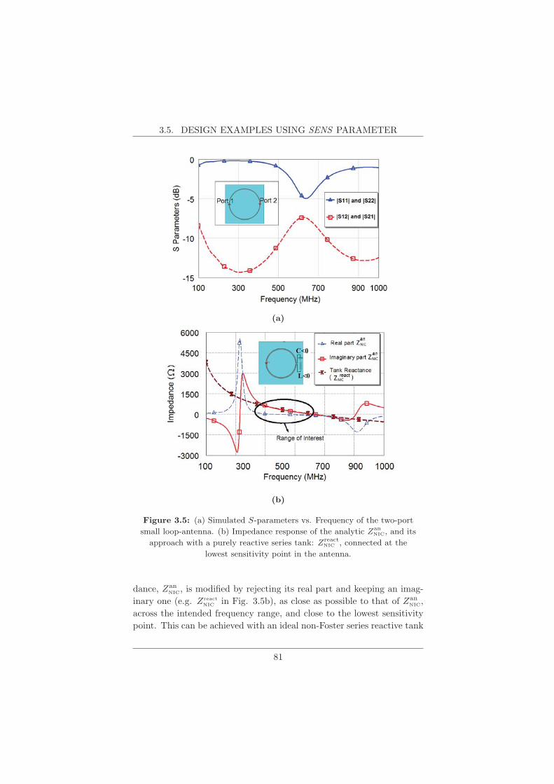
3.5. DESIGN EXAMPLES USING SENS PARAMETER
(a)
(b)
Figure 3.5: (a) Simulated S-parameters vs. Frequency of the two-port
small loop-antenna. (b) Impedance response of the analytic ZanNIC, and its
approach with a purely reactive series tank: ZreactNIC , connected at the
lowest sensitivity point in the antenna.
dance, ZanNIC, is modified by rejecting its real part and keeping an imag-
inary one (e.g. Zreact
NIC in Fig. 3.5b), as close as possible to that of ZanNIC,
across the intended frequency range, and close to the lowest sensitivity
point. This can be achieved with an ideal non-Foster series reactive tank
81
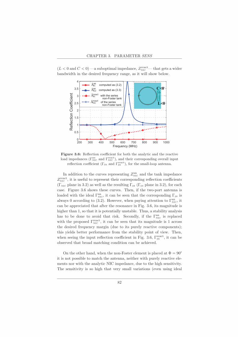
CHAPTER 3. PARAMETER SENS
(L < 0 and C < 0) —a suboptimal impedance, ZreactNIC — that gets a wider
bandwidth in the desired frequency range, as it will show below.
Frequency (MHz)
ĀNIC computed as (3.3)
ĀIN with the series non-Foster tankĀNIC of the series non-Foster tank
ĀIN computed as (3.2)an
an
react
react
Figure 3.6: Reflection coefficient for both the analytic and the reactive
load impedances (ΓanNIC and Γreact
NIC ), and their corresponding overall input
reflection coefficient (ΓIN and ΓreactIN ), for the small-loop antenna.
In addition to the curves representing ZanNIC and the tank impedance
ZreactNIC , it is useful to represent their corresponding reflection coefficients
(ΓNIC plane in 3.2) as well as the resulting ΓIN (ΓIN plane in 3.2), for each
case. Figure 3.6 shows these curves. Then, if the two-port antenna is
loaded with the ideal ΓanNIC, it can be seen that the corresponding ΓIN is
always 0 according to (3.2). However, when paying attention to ΓanNIC, it
can be appreciated that after the resonance in Fig. 3.6, its magnitude is
higher than 1, so that it is potentially unstable. Thus, a stability analysis
has to be done to avoid that risk. Secondly, if the ΓanNIC is replaced
with the proposed ΓreactNIC , it can be seen that its magnitude is 1 across
the desired frequency margin (due to its purely reactive components);
this yields better performance from the stability point of view. Then,
when seeing the input reflection coefficient in Fig. 3.6, ΓreactIN , it can be
observed that broad matching condition can be achieved.
On the other hand, when the non-Foster element is placed at Φ = 90
it is not possible to match the antenna, neither with purely reactive ele-
ments nor with the analytic NIC impedance, due to the high sensitivity.
The sensitivity is so high that very small variations (even using ideal
82
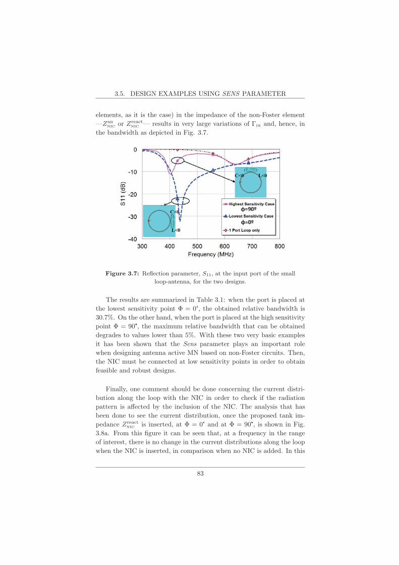
3.5. DESIGN EXAMPLES USING SENS PARAMETER
elements, as it is the case) in the impedance of the non-Foster element
—ZanNIC or Zreact
NIC — results in very large variations of ΓIN and, hence, in
the bandwidth as depicted in Fig. 3.7.
Figure 3.7: Reflection parameter, S11, at the input port of the small
loop-antenna, for the two designs.
The results are summarized in Table 3.1: when the port is placed at
the lowest sensitivity point Φ = 0�, the obtained relative bandwidth is
30.7%. On the other hand, when the port is placed at the high sensitivity
point Φ = 90�, the maximum relative bandwidth that can be obtained
degrades to values lower than 5%. With these two very basic examples
it has been shown that the Sens parameter plays an important role
when designing antenna active MN based on non-Foster circuits. Then,
the NIC must be connected at low sensitivity points in order to obtain
feasible and robust designs.
Finally, one comment should be done concerning the current distri-
bution along the loop with the NIC in order to check if the radiation
pattern is affected by the inclusion of the NIC. The analysis that has
been done to see the current distribution, once the proposed tank im-
pedance ZreactNIC is inserted, at Φ = 0� and at Φ = 90�, is shown in Fig.
3.8a. From this figure it can be seen that, at a frequency in the range
of interest, there is no change in the current distributions along the loop
when the NIC is inserted, in comparison when no NIC is added. In this
83
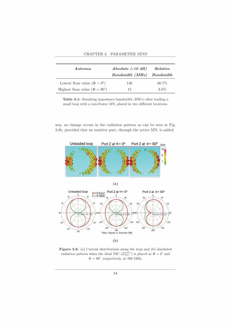
CHAPTER 3. PARAMETER SENS
Antenna Absolute (-10 dB) Relative
Bandwidth (MHz) Bandwidth
Lowest Sens value (Φ = 0�) 146 30.7%
Highest Sens value (Φ = 90�) 15 3.8%
Table 3.1: Resulting impedance bandwidth (BWv) after loading a
small loop with a non-Foster MN, placed in two different locations.
way, no change occurs in the radiation pattern as can be seen in Fig.
3.8b, provided that no resistive part, through the active MN, is added.
(a)
(b)
Figure 3.8: (a) Current distributions along the loop and (b) simulated
radiation pattern when the ideal NIC (ZreactNIC ) is placed at Φ = 0� and
Φ = 90�, respectively, at 500 MHz.
84
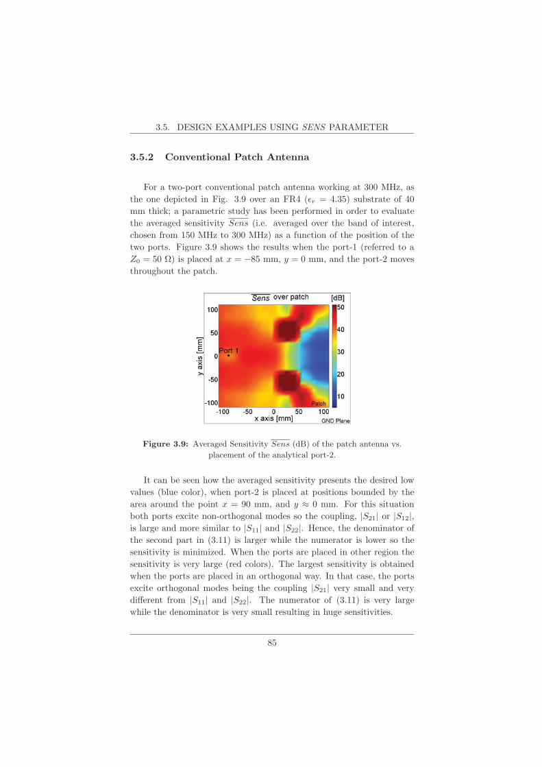
3.5. DESIGN EXAMPLES USING SENS PARAMETER
3.5.2 Conventional Patch Antenna
For a two-port conventional patch antenna working at 300 MHz, as
the one depicted in Fig. 3.9 over an FR4 (εr = 4.35) substrate of 40
mm thick; a parametric study has been performed in order to evaluate
the averaged sensitivity Sens (i.e. averaged over the band of interest,
chosen from 150 MHz to 300 MHz) as a function of the position of the
two ports. Figure 3.9 shows the results when the port-1 (referred to a
Z0 = 50 Ω) is placed at x = −85 mm, y = 0 mm, and the port-2 moves
throughout the patch.
Figure 3.9: Averaged Sensitivity Sens (dB) of the patch antenna vs.
placement of the analytical port-2.
It can be seen how the averaged sensitivity presents the desired low
values (blue color), when port-2 is placed at positions bounded by the
area around the point x = 90 mm, and y ≈ 0 mm. For this situation
both ports excite non-orthogonal modes so the coupling, |S21| or |S12|,is large and more similar to |S11| and |S22|. Hence, the denominator of
the second part in (3.11) is larger while the numerator is lower so the
sensitivity is minimized. When the ports are placed in other region the
sensitivity is very large (red colors). The largest sensitivity is obtained
when the ports are placed in an orthogonal way. In that case, the ports
excite orthogonal modes being the coupling |S21| very small and very
different from |S11| and |S22|. The numerator of (3.11) is very large
while the denominator is very small resulting in huge sensitivities.
85

CHAPTER 3. PARAMETER SENS
Considering the value of ZanNIC and its feasibility of implementation,
the lowest sensitivity point (x = 110 mm, y = 0 mm, Sens = 4.02 dB)
has to be discarded, because of the need of three non-Foster elements to
fulfill ZanNIC, as it is depicted in Fig. 3.10 with a series combination of a
negative inductor with a negative parallel LC tank.
Figure 3.10: ZanNIC and an ideal non-Foster realization of Zreact
NIC at
x = 100 mm, y = 0 mm.
Another possible design is studied for the point x = 27 mm, y = 0
mm, Sens = 20 dB. Figure 3.11a shows the analytic impedance, ZanNIC,
and the approximation obtained using ideal non-Foster elements when
connected at this last point. It can be seen that this is the most feasible
design since it only needs a negative parallel LC tank comprised of two
non-Foster elements —instead of three of them— to realize ZreactNIC . It is
important to remark, as mentioned in previous sections, that the sensi-
tivity Sens depends on the frequency as the S-parameters do, as shown
in Fig. 3.11b. Moreover, the magnitude of Sens keeps lower than 12
dB —a reasonable value— over the desired bandwidth (150 MHz to 300
MHz) when the port-2 is located at x = 27 mm, y = 0 mm.
The obtained reflection parameter (S11) for both the loaded and the
NIC-loaded antenna is shown in Fig. 3.12.
The planar nature of the patch antenna structure requires an analysis
of the current distribution, after including the non-Foster network at
port-2, to see if the active matching modifies the radiation pattern. Fig.
3.13a shows a change in the current distribution at 200 MHz for the
86

3.5. DESIGN EXAMPLES USING SENS PARAMETER
(a)
Frequency (MHz)
(b)
Figure 3.11: (a) ZanNIC and an ideal non-Foster approximation, Zreact
NIC ,
at x = 27 mm, y = 0 mm. (b) Sensitivity Sens and |S|-parameters vs.
Frequency when the port-2 is located at x = 27 mm, y = 0 mm.
conventional patch antenna when it is loaded with ZreactNIC . It can be seen
that for the loaded case there is a maximum of current in the middle
of the patch what leads to the monopolar-like radiation pattern seen in
Fig. 3.13b, different from the one expected in a frequency away from
resonance one, for a conventional patch antenna (i.e. a magnetic dipole-
like pattern).
87

CHAPTER 3. PARAMETER SENS
Figure 3.12: |S11| for the unloaded and 2-port patch with ZreactNIC .
(a)
dBi
xz
y y
xz
Unloaded PatchPatch loaded with ZreactNIC
(b)
Figure 3.13: (a) Current distribution at 200 MHz for the conventional
patch antenna. (b) Simulated radiation patterns for both the loaded
with ZreactNIC patch with the unloaded case, respectively, with a small
ground plane.
88
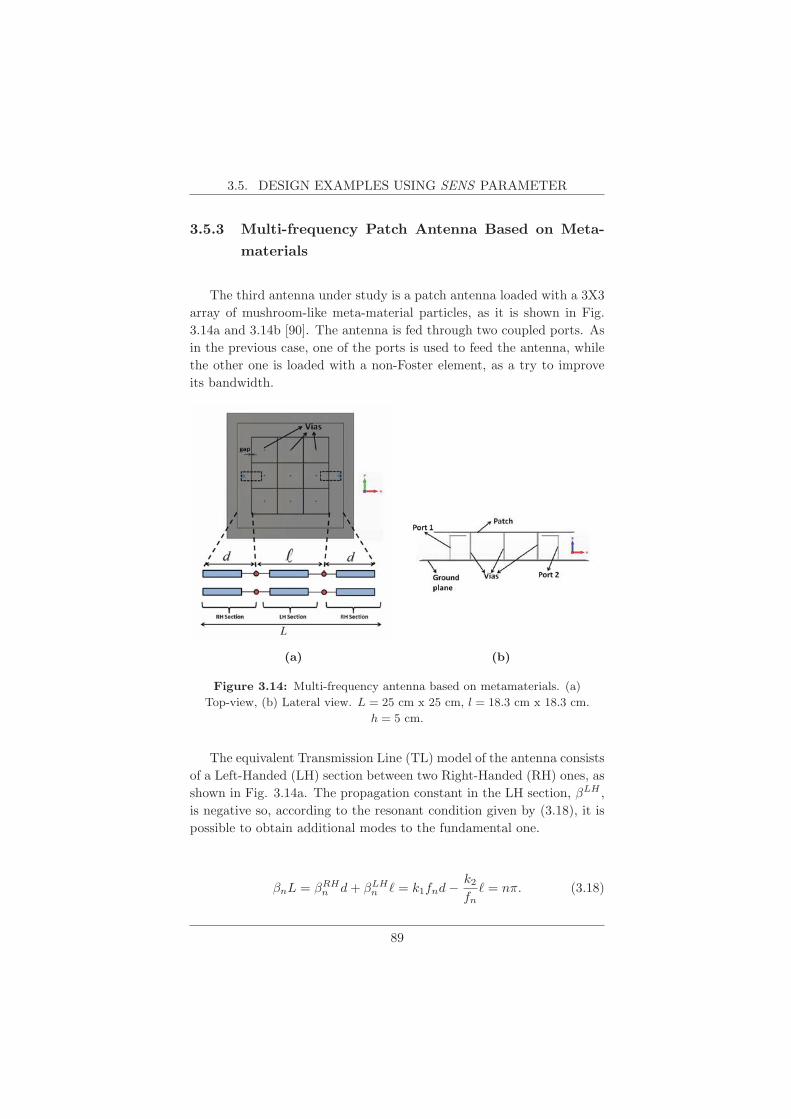
3.5. DESIGN EXAMPLES USING SENS PARAMETER
3.5.3 Multi-frequency Patch Antenna Based on Meta-
materials
The third antenna under study is a patch antenna loaded with a 3X3
array of mushroom-like meta-material particles, as it is shown in Fig.
3.14a and 3.14b [90]. The antenna is fed through two coupled ports. As
in the previous case, one of the ports is used to feed the antenna, while
the other one is loaded with a non-Foster element, as a try to improve
its bandwidth.
(a) (b)
Figure 3.14: Multi-frequency antenna based on metamaterials. (a)
Top-view, (b) Lateral view. L = 25 cm x 25 cm, l = 18.3 cm x 18.3 cm.
h = 5 cm.
The equivalent Transmission Line (TL) model of the antenna consists
of a Left-Handed (LH) section between two Right-Handed (RH) ones, as
shown in Fig. 3.14a. The propagation constant in the LH section, βLH ,
is negative so, according to the resonant condition given by (3.18), it is
possible to obtain additional modes to the fundamental one.
βnL = βRHn d+ βLH
n � = k1fnd− k2fn
� = nπ. (3.18)
89
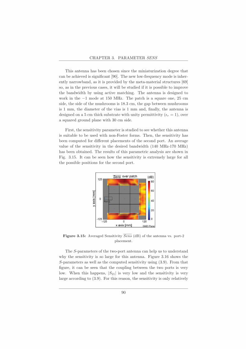
CHAPTER 3. PARAMETER SENS
This antenna has been chosen since the miniaturization degree that
can be achieved is significant [90]. The new low-frequency mode is inher-
ently narrowband, as it is provided by the meta-material structures [69]
so, as in the previous cases, it will be studied if it is possible to improve
the bandwidth by using active matching. The antenna is designed to
work in the −1 mode at 150 MHz. The patch is a square one, 25 cm
side, the side of the mushrooms is 18.3 cm, the gap between mushrooms
is 1 mm, the diameter of the vias is 1 mm and, finally, the antenna is
designed on a 5 cm thick substrate with unity permittivity (εr = 1), over
a squared ground plane with 30 cm side.
First, the sensitivity parameter is studied to see whether this antenna
is suitable to be used with non-Foster forms. Then, the sensitivity has
been computed for different placements of the second port. An average
value of the sensitivity in the desired bandwidth (140 MHz-170 MHz)
has been obtained. The results of this parametric analysis are shown in
Fig. 3.15. It can be seen how the sensitivity is extremely large for all
the possible positions for the second port.
Figure 3.15: Averaged Sensitivity Sens (dB) of the antenna vs. port-2
placement.
The S-parameters of the two-port antenna can help us to understand
why the sensitivity is so large for this antenna. Figure 3.16 shows the
S-parameters as well as the computed sensitivity using (3.9). From that
figure, it can be seen that the coupling between the two ports is very
low. When this happens, |S21| is very low and the sensitivity is very
large according to (3.9). For this reason, the sensitivity is only relatively
90
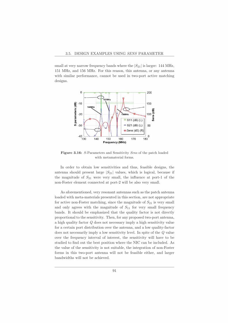
3.5. DESIGN EXAMPLES USING SENS PARAMETER
small at very narrow frequency bands where the |S21| is larger: 144 MHz,
151 MHz, and 156 MHz. For this reason, this antenna, or any antenna
with similar performance, cannot be used in two-port active matching
designs.
Figure 3.16: S-Parameters and Sensitivity Sens of the patch loaded
with metamaterial forms.
In order to obtain low sensitivities and thus, feasible designs, the
antenna should present large |S21| values, which is logical, because if
the magnitude of S21 were very small, the influence at port-1 of the
non-Foster element connected at port-2 will be also very small.
As aforementioned, very resonant antennas such as the patch antenna
loaded with meta-materials presented in this section, are not appropriate
for active non-Foster matching, since the magnitude of S21 is very small
and only agrees with the magnitude of S11 for very small frequency
bands. It should be emphasized that the quality factor is not directly
proportional to the sensitivity. Then, for any proposed two-port antenna,
a high quality factor Q does not necessary imply a high sensitivity value
for a certain port distribution over the antenna, and a low quality-factor
does not necessarily imply a low sensitivity level. In spite of the Q value
over the frequency interval of interest, the sensitivity will have to be
studied to find out the best position where the NIC can be included. As
the value of the sensitivity is not suitable, the integration of non-Foster
forms in this two-port antenna will not be feasible either, and larger
bandwidths will not be achieved.
91

CHAPTER 3. PARAMETER SENS
Although from the sensitivity analysis it has already been concluded
that it is not possible to integrate a non-Foster network with this an-
tenna, a final analysis on the current distribution and on the correspond-
ing radiation pattern is also presented. Figure 3.17a shows the compar-
ison between the simulated current distributions at 144 MHz when the
patch is loaded with ZreactNIC , at the symmetrically located port-2 (with
respect to port-1), and the unloaded patch. It can be seen that for
the case of loading with the non-Foster element (reactive case) there
is a maximum of current in the middle of the patch which leads to a
monopolar-like radiation pattern, instead of the typical dipolar-like one
associated to the metamaterial patch with no loading, seen in Fig. 3.17b.
3.6 Conclusion
Finally, it can be concluded that in intervals of frequency at which
the antenna is non-resonant, as in the case of the small loop and the
conventional patch antenna presented in sections 3.5.1 and 3.5.2, respec-
tively, the active non-Foster matching is feasible. These antennas present
similar values of S11 and S21 over larger bandwidths so that the sensi-
tivity is also kept low over such bandwidths, making broadband designs
possible. The level of degradation in the antenna efficiency is intimately
related to the real part of ZanNIC, therefore, this parameter should be kept
low over the frequency range of interest.
It has been shown that the sensitivity Sens is a very important design
parameter that can be stated as the starting point of a complete design
procedure for actively matched antennas, loaded with non-Foster forms.
Then, a procedure for carrying out the sensitivity analysis can be listed
as follows:
1. Draw or model the desired antenna structure for extracting a two-
port S-parameters matrix, for different point inside the antenna.
2. Compute the sensitivity parameter, as in (3.9), over the frequency
interval of interest, at each port-2 location in the previous step, in
order to see whether the proposed antenna presents suitable points
to integrate a non-Foster form. In case so you can go ahead with
the following points (this happens, for instance, for the loop and
for the conventional patch but not for the metamaterial patch).
92
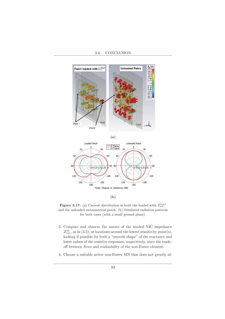
3.6. CONCLUSION
(a)
(b)
Figure 3.17: (a) Current distribution in both the loaded with ZreactNIC
and the unloaded metamaterial patch. (b) Simulated radiation patterns
for both cases (with a small ground plane).
3. Compute and observe the nature of the needed NIC impedance
ZanNIC, as in (3.5), at locations around the lowest sensitivity point(s),
looking if possible for both a “smooth shape” of the reactance and
lower values of the resistive responses, respectively, since the trade-
off between Sens and realizability of the non-Foster element.
4. Choose a suitable active non-Foster MN that does not greatly af-
93

CHAPTER 3. PARAMETER SENS
fect the efficiency of the antenna. For that reason, the impedance
chosen is a suboptimal one with reactive performance.
5. Study the current distribution in order to see that the radiation
modes are the same as in the original antenna (this happens for
the loop, loaded with ZreactNIC , but not for conventional patch or the
patch loaded with metamaterial particles).
In relation to previously reported works in literature, other authors have
implemented the embedded active non-Foster matching without check-
ing any influence on ZIN due to the location of the engineered non-Foster
MN. No especial concerns have been taken in relation with the NIC lo-
cation. In this sense, when embedding an active MN well in the antenna
structure itself —as in [42]— well in some parasitic/metamaterial struc-
ture in the near field —as in [38, 84] and [44]— the Sens parameter can
be helpful for finding the more suitable location for the non-Foster form.
The introduction of the sensitivity parameter, Sens, allows us to see
the dependence of the input impedance on the variations of that from
the NIC, with respect to the analytic one. The ports must be placed
at points of low sensitivity. In this way, small variations of the non-
Foster element, (variations in the NICs) will not degrade the matching
performance. Then, once a low sensitivity location is chosen, the design
must be made over a frequency range where the real part of ZanNIC has
low values in order not to degrade the antenna efficiency. If the ports
are placed in such a way that high sensitivities are obtained, the design
will not work properly, since any small variation in the implemented
non-Foster element (which are unavoidable in practice) will yield in high
variations of the input impedance, and hence, in the bandwidth.
Moreover, the feasibility must also be taken into account; because
in some placements the needed analytical impedance (specifically the
optimum reactance) is very difficult to achieve using practical NICs.
For this reason, a trade-off between sensitivity and feasibility should be
studied for each particular case. These last considerations have to be
included in the global design procedure, alongside the stability analysis,
as it will be shown in the next chapter with manufactured NIC circuits
embedded in real ESAs.
94

CHAPTER 4
DESIGN METHOD FOR NON-FOSTERACTIVELY MATCHED ESAS
4.1 Introduction
The current demand on more compact and broader bandwidth de-
vices makes necessary to improve the performance of small antennas.
A smart strategy for integrating non-Foster networks with ESAs, opti-
mizing its placement into the radiating structure while considering the
stability and radiation performance of the whole antenna system, will
always be welcome in communication systems.
As mentioned in Chapter 2, most of the previously reported works
include the use of non-Foster components at the terminals of dipole- or
monopole-like antennas. Even when some other authors have considered
embedding the non-Foster circuit (NFC) in the antenna structure, most
of the effort has been focused in optimizing and characterizing the NFC
—indeed one of the most challenging tasks— more than in analyzing the
complete antenna system.
In this sense, the present chapter aims at proposing a global method-
ology for the design of actively matched antennas. In this way, the an-
tenna and the non-Foster networks are considered a whole system. In

CHAPTER 4. DESIGN METHOD FOR ACTIVE-MN IN ESAS
addition to the impedance bandwidth improvement, the stability and
tolerance of the components, the current distributions, and the corre-
sponding radiation patterns are also considered.
4.2 An Integral Design Method
In this section, the proposed strategy is described. First, the antenna
to be integrated with a NFC undergoes the sensitivity analysis (devised
and described in the previous chapter) to see whether the antenna is
suitable for it or not. Additionally, this sensitivity analysis will also
determine the most appropriate place for the NIC. Second, not all the
non-Foster networks are valid for being integrated with the antenna, so
some remarks on the non-Foster network are provided in order to choose
the most suitable one. Third, a trustworthy stability analysis of the
overall structure (NIC + antenna) shall be done.
It is important to emphasize that the stability analysis has to be
done in the overall structure since the antenna loading can modify the
overall performance of the NIC stability. Fourth, the radiation pattern
of the integrated antenna has to be studied; this analysis is undertaken
by studying the variations of the current distributions in the original an-
tenna. Finally, since any change in the actual value of the components
in the NIC can modify the performance, well the stability well the sensi-
tivity of the overall structure, a tolerance analysis is welcome in order to
predict potential and uncontrolled variations. Figure 4.1 shows a sketch
of the previously described design strategy.
4.2.1 Step 1: Sensitivity Analysis
For the sake of conciseness and clarity, the complete deduction of
the Sens parameter is omitted in this chapter since it was presented in
Chapter 3. Nonetheless, it should be mentioned that as the first step
in the design strategy, it is necessary to add an analytical second port
to the antenna itself, where the active MN is to be placed. Figure 4.2
depicts the CAD model of the patch antenna, previously described in
Section 3.5.2, in which the fictitious port-2 is added. The swept sketched
in Fig. 4.2 indicates those port-2 locations over the patch from which
96

4.2. AN INTEGRAL DESIGN METHOD
Figure 4.1: Summary of the proposed strategy.
a number n of S-parameters matrices will be extracted, after the full-
wave simulation. Thus, each point of the swept gives a two-port network
version of the patch that can be analyzed under the non-Foster matching
approach, depicted in Fig. 4.3. Once the S-parameters matrices have
been extracted, it is possible to compute the Sens parameter as in (3.9),
whose expression is shown here again, as follows:
Sens =
∣∣∣∣ S21S12
(1− S22ΓNIC)2
∣∣∣∣∣∣∣∣ΓNIC=Γan
NIC
=
∣∣∣∣ (S11S22 − S21S12)2
S21S12
∣∣∣∣ . (4.1)
As mentioned in Chapter 3, the Sens parameter only depends on the
S-parameters of the two-port antenna. Not only the suitability of the
proposed antenna is inferred by computing Sens at different points over
the structure, but also the most convenient port location for the resulting
two-port network. It should be pointed out that there is no need of an
analytical circuit model for the antenna, difficult to extract in practice;
this fact facilitates and generalizes the design process to many types of
antennas since they just have to be drawn in an electromagnetic CAD
software. In addition, it is possible to extend the active non-Foster MN
approach of two-port antennas to any other actively embedded-matched
antenna approaches, like the ones reported in the literature [38,42,44,91].
97
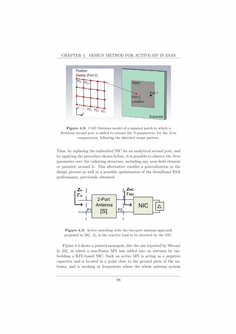
CHAPTER 4. DESIGN METHOD FOR ACTIVE-MN IN ESAS
Port 2Location
PositionSweep (Port-2)
Port 1
Patch
Substratex
yP22 P21
P23...
P2n-1P2n
Figure 4.2: CAD Antenna model of a squared patch in which a
fictitious second port is added to extract the S-parameters, for the Sens
computation, following the sketched swept pattern.
Thus, by replacing the embedded NIC for an analytical second port, and
by applying the procedure shown before, it is possible to observe the Sens
parameter over the radiating structure, including any near-field element
or parasitic around it. This alternative enables a generalization in the
design process as well as a possible optimization of the broadband ESA
performance, previously obtained.
Figure 4.3: Active matching with the two-port antenna approach
proposed in [86]. ZL is the reactive load to be inverted by the NIC.
Figure 4.4 shows a printed monopole, like the one reported by Mirzaei
in [42], in which a non-Foster MN was added into an antenna by em-
bedding a BJT-based NIC. Such an active MN is acting as a negative
capacitor and is located in a point close to the ground plate of the an-
tenna, and is working at frequencies where the whole antenna system
98

4.2. AN INTEGRAL DESIGN METHOD
is electrically small since the ka factor is lower than 0.5. Experimental
results are also reported. The colored area in the monopole depicts the
Sens parameter, computed as (4.1), averaged over the same frequency
interval used by the authors in [42] at which the NIC is working (250
MHz to 500 MHz). Then, in order to extend our approach to the de-
scribed work, the NFC in [42] is replaced here by an analytical second
port. Thus, once the one-port monopole is treated as a two-port an-
tenna, the port-2 location sweep takes place over several points in the
antenna, leading to the observation of Sens. It is possible to infer that
the closer the NIC is located to the bottom edge of the monopole, the
lower the Sens parameter is. Then, the point located by the authors
in [42] can be considered as a good option to embed the non-Foster MN.
Port-2
Substrate
GNDFeedport (P1)
(dB)40
30
20
1010.6 cm
4.8 cm
Sens
Figure 4.4: Averaged Sens parameter depicted over the printed slotted
monopole proposed in [42]. The blue area represents the lower sensitivity
points to embed the NIC.
Figure 4.5 shows a similar type of antenna —a printed monopole—
reported in [38], but with the non-Foster MN acting as a negative induc-
tor, and embedded in a near field resonant parasitic (NFRP) element: an
Egyptian-Axe-shaped parasite. The NFRP is located on the bottom face
of the substrate, opposite to the one of the monopole. At the resonant
frequency added by the NFRP (300 MHz), the antenna size is such that
a ka factor of 0.49 is checked. The reported NIC is a BJT-based one,
working from 200 MHz to 400 MHz, added to broaden the resonance of
the overall antenna, according to the reported simulations. That is, the
99
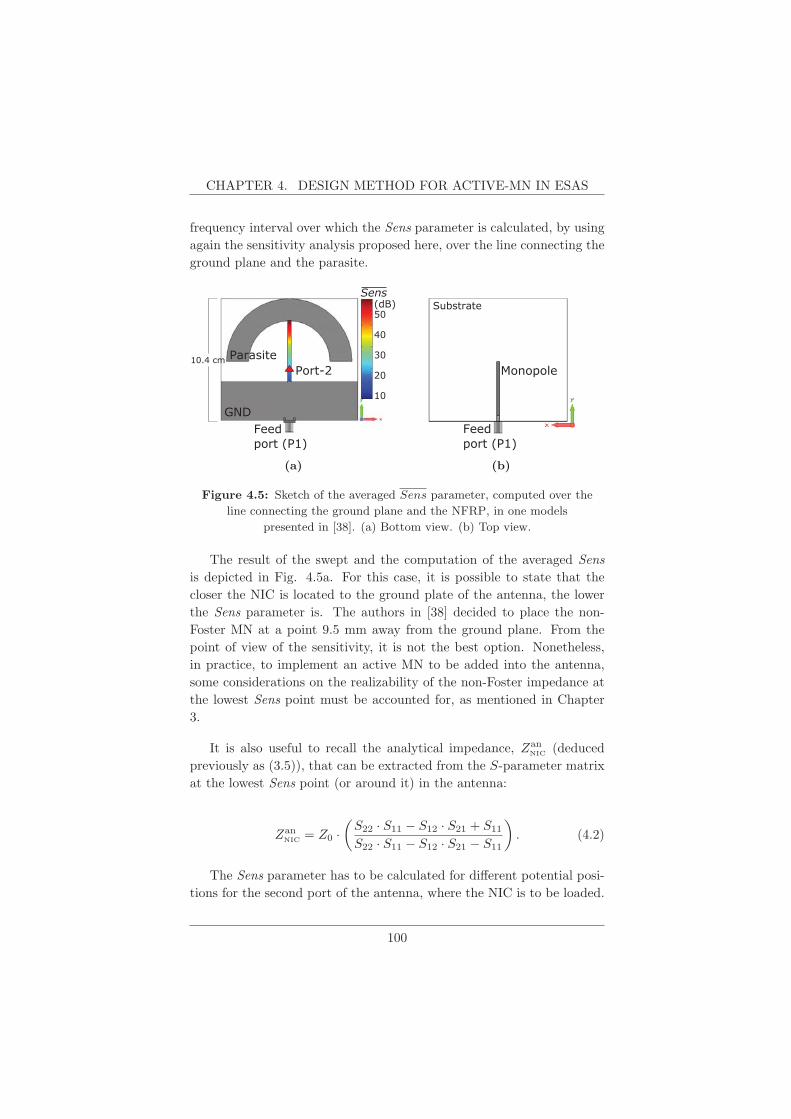
CHAPTER 4. DESIGN METHOD FOR ACTIVE-MN IN ESAS
frequency interval over which the Sens parameter is calculated, by using
again the sensitivity analysis proposed here, over the line connecting the
ground plane and the parasite.
(dB)50
40
30
20
10
Port-2
GNDFeedport (P1)
Parasite10.4 cm
Sens
(a)
Substrate
Monopole
Feedport (P1)
(b)
Figure 4.5: Sketch of the averaged Sens parameter, computed over the
line connecting the ground plane and the NFRP, in one models
presented in [38]. (a) Bottom view. (b) Top view.
The result of the swept and the computation of the averaged Sens
is depicted in Fig. 4.5a. For this case, it is possible to state that the
closer the NIC is located to the ground plate of the antenna, the lower
the Sens parameter is. The authors in [38] decided to place the non-
Foster MN at a point 9.5 mm away from the ground plane. From the
point of view of the sensitivity, it is not the best option. Nonetheless,
in practice, to implement an active MN to be added into the antenna,
some considerations on the realizability of the non-Foster impedance at
the lowest Sens point must be accounted for, as mentioned in Chapter
3.
It is also useful to recall the analytical impedance, ZanNIC (deduced
previously as (3.5)), that can be extracted from the S-parameter matrix
at the lowest Sens point (or around it) in the antenna:
ZanNIC = Z0 ·
(S22 · S11 − S12 · S21 + S11
S22 · S11 − S12 · S21 − S11
). (4.2)
The Sens parameter has to be calculated for different potential posi-
tions for the second port of the antenna, where the NIC is to be loaded.
100
4.2. AN INTEGRAL DESIGN METHOD
The optimal choice is that at which the sensitivity is minimized, which
implies that changes in the NIC will not greatly affect the input impe-
dance. Otherwise, any small change in the impedance provided by the
NIC will dramatically affect the antenna performance in terms of the
overall matching bandwidth. This step is critical since not all the anten-
nas neither the positions in them are suitable for including non-Foster
matching networks.
4.2.2 Step 2: NIC Topology Considerations
The NIC selection comprises not only the frequency range of opera-
tion of transistors but the type of circuit connection (grounded or float-
ing) and the fabrication technology as well. The non-Foster behavior of
a NIC is usually expected to be a small fraction of the high-frequency
parameter, fT [23,67] —the gain bandwidth product defined as that fre-
quency at which hfe = 1 (0 dB) [92]. This, in turn, allow keeping low the
influence of internal capacitances (Cπ, Cμ in the BJT or Cgs in the FET)
on the NIC impedance response, as shown before in Section 2.7.2. On the
other hand, especially in balanced-NIC configurations, a transistor with
a fT lower than the frequency of possible oscillations predicted for the
manufactured circuit is preferred [93]. Such oscillation can result from
currents in the even mode, operating across the feedback paths between
the transistors. As a general rule, short feedback path-lengths should be
implemented to bring the potential oscillations into higher frequencies,
out of the working range of the transistors [93].
In addition, floating or grounded NIC configurations may be selected
depending on the sensitivity analysis results. Then, if the lowest sensitiv-
ity point in the antenna is found to be near the ground plane (if it exists),
a grounded configuration will be easier to build, especially for the DC
return path from the bias network. Nevertheless, grounded configuration
produces important changes in the current distribution of the antenna,
especially in planar structures, as it was shown in the previous chapter.
This implies that for antennas such as patches or printed monopoles, un-
desired changes in the radiation pattern of the actively matched antenna
can arise. Among these changes, it could be mentioned additional lobes
or nulls, or even an entire different radiation mode. This phenomenon is
due to the presence of an additional path to ground for the currents at
101

CHAPTER 4. DESIGN METHOD FOR ACTIVE-MN IN ESAS
frequencies where the NIC is working.
Additionally, it is necessary to decide which port of the NIC itself
is appropriate to be connected inside the antenna. Since the embedded
negative capacitor/inductor circuit is intended to compensate the effec-
tive capacitance/inductance of the corresponding ESA, the impedance
seen by the NIC at certain port-2 location (Zs in Fig. 4.7a) must sat-
isfy the first necessary condition for stability, accordingly to the Linvill
criteria [19].
Z2Z1
Z3 Z4
OCS Ports
SCS Ports
Q1 Q2
ZIN(P4)
ZIN(P2)
ZIN(P3)
ZIN(P1)
Figure 4.6: General topology of a NIC circuit with the input
impedances when looking into each of the four ports
These criteria state the classification of the NIC ports in two
types: Open Circuit Stable (OCS) or Short Circuit Stable (SCS). Each
one of these types states a condition on the external loading impe-
dance/admittance magnitude to avoid any pole of the system lying in
the complex Right Half-Plane (RHP). The system results of connect-
ing the NIC with the antenna or with any other passive device. Figure
4.6 [70] shows a generalized and conventional NIC schematic consisting
of two cross-coupled BJTs. The OCS or SCS classification at each port
are shown as well. Then, both the stability condition and the input
impedance can be calculated, as follows
102

4.2. AN INTEGRAL DESIGN METHOD
Stability Condition Input Impedance
|ZIN(P1)| < |Z1|; ZIN(P1) = −Z3 · Z4
Z2,
|ZIN(P2)| < |Z2|; ZIN(P2) = −Z3 · Z4
Z1,
|ZIN(P3)| > |Z3|; ZIN(P3) = −Z1 · Z2
Z4,
|ZIN(P4)| > |Z4|; ZIN(P4) = −Z1 · Z2
Z3.
(4.3)
Is important to note that there are two different ways to connect a
NIC into an active MN, depending on which ports are used to couple the
signal. Thus, if the NIC is connected —or embedded— to the antenna
through the ports 1 and 2, in Fig. 4.6, it is going to work in a balanced-
OCS configuration. On the other hand, if ports 3 and 4 are selected,
the NIC will work in a balanced-SCS configuration. For the case of a
grounded active MN, if ports 1 or 2 are selected to act as ZNIC, the NIC
is going to work in an unbalanced-OCS configuration, while ports 3 and
4 will set the NIC in an unbalanced-SCS configuration.
Thus, deciding which port (or ports) to use to perform the NIC as
an active MN is an important task. Conventionally, for example, in a
series configuration where the NIC is connected at the feeding point of
the ESA (as depicted in Fig. 2.18b), the antenna impedance nature
have to be analyzed first. For instance, in a small monopole, whose
impedance is highly capacitive at lower frequencies, a balanced-OCS
NIC is used [39–41]. If the parallel connection of the NIC at the feeding
point of the ESA is chosen, the unbalanced-SCS configuration is more
appropriate [75]. In embedded active MNs, the magnitude of the analytic
NIC impedance, ZanNIC, computed as (3.7), should be observed prior to
choosing which port —or ports— of the NIC is going to be used either
in the floating or in the grounded configuration. The concepts of OCS
and SCS are further described in Step 3.
On the other hand, floating NIC configuration produces substantially
lower changes in the radiation pattern, but with the drawback of higher
values of sensitivity that implies, as aforementioned, poor impedance
103
CHAPTER 4. DESIGN METHOD FOR ACTIVE-MN IN ESAS
matching performance. In addition, larger stability problems may also
arise for floating structures, as mentioned in [19] and [39]. Then, a trade-
off for the NIC selection has to be made to choose, both, the transistor
(by considering its transition frequency) and the topology (grounded
or floating) for the NIC, keeping in mind the location of the lowest
sensitivity point in the antenna structure.
4.2.3 Step 3: Stability Analysis
It is well known that stability is a time-domain property of cir-
cuits [94], in such a way that every bounded input yields a bounded
output as time approaches infinity. However, when the frequency of op-
eration rises, the time-domain methods lack of practicality to be applied,
thus, a frequency-domain technique is preferable, in order to account for
dispersion of components, parasitics, and a very important parameter:
the modeling of the inside active devices. In this sense, a number of re-
ported works dealing with the circuit stability can be found [22,95–100].
All these methods are based on the Nyquist criterion [101] to check if
the corresponding network function does not have any poles lying in the
RHP of the s-plane.
On the other hand, the stability analysis is critical when non-
Foster circuits are present due to the positive feedback involved in the
transistor-based realizations. The situation, when including the non-
Foster circuit inside the antenna, is somewhat more critical than when
considering the NIC itself as an outer part of a matching circuit. In
this case, the antenna and the non-Foster circuit cannot be separated,
in such a way that the simple analysis based on classical Linvill crite-
ria [19], is no longer enough. However, the analysis on evaluating OCS or
SCS constitute a necessary but non-sufficient condition for the stability
verification.
To analyze the stability, Linvill used the equivalent circuit model of
the BJT, and separate the analysis of the balanced topology he presented
in two cases [19]. The first one accounts for the case when the input is
taken from the emitter-terminals (ports 1 and 2 in Fig. 4.6). Then, the
input impedance, ZNIC, of this configuration is analyzed to verify the fact
that it has no poles in the RHP, according to the reasoning presented
104

4.2. AN INTEGRAL DESIGN METHOD
ZL
ZS ZNIC=-kZL
ZS
Referenceplane
NIC
(a)
YNIC=-YL/kYS
YL
k>0
YS
Referenceplane
NIC
(b)
Figure 4.7: Ideal NIC diagram showing the reference plane for (a)
open-circuit and (b) short-circuit stability verification.
by Merrill in [61]. Linvill concluded that, in this configuration, depicted
in Fig. 4.7a, the open-circuit stability is verified. In other words, that
an OCS-NIC will have all input impedance poles in the Left Half-Plane
(LHP). This configuration leads to stability when the NIC is connected
to an external impedance Zs, providing |ZNIC| < |Zs|, which is the OCS
condition. Likewise, in the second case, the input admittance of the NIC,
YNIC, was analyzed when the input is taken from the collector-terminals
(ports 3 and 4 in Fig. 4.6). In this case, the stability is verified as
the fact that YNIC has no poles in the s-plane RHP. This configuration,
depicted in Fig. 4.7b, leads to stability when the NIC is connected to a
source admittance Ys, providing |YNIC| < |Ys|: the SCS condition. Then,
a SCS-NIC will have all input admittance poles in the LHP. These two
conditions are described in more detail below.
Let us particularize these criteria for the current situation where the
non-Foster circuit is embedded in the antenna itself. For this situation,
the block diagram in Fig. 4.3 is modified to see what is the impedance
seen at the reference plane, between the NIC circuit and the analytical
two-port network of the antenna (extracted in Step 1). This can be seen
in Fig. 4.8 where the actual antenna input port (P1) is loaded with the
receiver impedance that is transformed by a bilinear S-parameter trans-
formation in a new Zs impedance at port-2 (P2). ZRX is the impedance
of the receptor —or the subsequent stage in the reception system— as-
sumed to equal, by simplicity, the reference impedance of the system,
Z0.
105

CHAPTER 4. DESIGN METHOD FOR ACTIVE-MN IN ESAS
ZRX ZLTwo Port Antenna NIC
ZIN ZSZNIC=-kZL(YNIC=1/-kZL)
(YS)
Referenceplane
Figure 4.8: Reference plane in the two-port antenna approach for
evaluating the classical Linvill stability analysis.
The so-called OCS condition states that the stability of the NIC is
that the absolute value of the impedance at the left side of the reference
plane (ZS), should satisfy the following condition for all frequencies at
which the NIC can effectively negate ZL:
|Zs| ≥ |ZNIC| or |Ys| ≤ |YNIC| OCS port. (4.4)
If we consider the circuit mesh formed around reference plane (slotted
line in Fig. 4.8), it is possible to observe that the total impedance
is Zs − ZNIC. If the NIC impedance should equals Zs, a voltage source
would call for infinite current, an impossible condition [61]. The negative
difference between the magnitude of those impedances (|Zs|−|ZNIC| < 0)
can lead to oscillation, so the inequities in (4.4) are valid to describe the
OCS condition.
For the short-circuit stability, a necessary condition for the NIC to
be stable is that the absolute value of the admittance at the reference
plane (Ys), should satisfy the following condition for all frequencies at
which the NIC can effectively negate ZL:
|Ys| ≥ |YNIC| or |Zs| ≤ |ZNIC| SCS port. (4.5)
In this case, by considering the node currents flowing from the ref-
erence plane in Fig. 4.8, if a SCS port is selected to be connected to
106
4.2. AN INTEGRAL DESIGN METHOD
the two-port antenna block, the total admittance is Ys + YNIC. Then, if
the NIC admittance were equal to Ys, a current source would produce
an infinite voltage, an impossible condition. The negative difference be-
tween the magnitude of those admittances (|Ys| − |YNIC| < 0) can lead
to oscillation, so the inequities in (4.5) are valid to describe the SCS
condition.
Previous analysis suffers from two drawbacks, first of all, the analysis
on OCS or SCS criterion does not take into consideration important
factors such as the reactive nature of the NIC load, the dispersion of the
circuit components with frequency or the locus of the trace associated
with the network function. Furthermore, as the non-Foster circuit is
embedded in the antenna, there is no actual access to that point. Those
are the reasons because of that the OCS-SCS validation constitutes a
necessary but non-sufficient condition for stability in an actively loaded
antenna system [102].
In addition, at microwave frequencies, besides the study of a corre-
sponding transfer function, other parameters have to be used to predict
stability since it is difficult to obtain the voltage or current transfer
functions for applying to them the Nyquist criteria.
In this sense, other conventional parameters have been proposed to
evaluate stability in microwave circuits such as Rollet [103] K −Δs pair
(where Δs is the determinant of the system function in the s domain),
or the μ factor. These parameters are functions of reduced two-port rep-
resentations in terms of the S-parameters —but also applicable with z -,
y or h-parameters— which look for unconditional stability by ensuring
that the input/output impedances of the system are positive real. The
K and the μ factors depend on which port (input or output) the analysis
is carried out.
The K factor, proposed in [103], is a scalar dimensionless quantity
that must be greater than 1, for all the frequencies at which the circuit is
intended to work, provided |Δs| < 1, to indicate that the loaded circuit
is stable. It can be computed as follows
K =1− |S11|2 − |S22|2 + |Δs|2
2|S12||S21| , (4.6)
107

CHAPTER 4. DESIGN METHOD FOR ACTIVE-MN IN ESAS
where
Δs = |S11S22 − S12S21|. (4.7)
The μ parameter, proposed in [104], comprises a geometrical ap-
proach that represent the previous criteria by the single condition
μ =1− |S11|
|S22 −ΔsS∗11|+ |S12S21| > 1. (4.8)
The main drawback of these parameters is the fact that they dis-
regard characteristics of more complex elements, as they are based on
characterized devices (e.g. transistors) known to be stable under dedi-
cated measurement fixtures [105]. In other words, these criteria fail due
to the use of a reduced two-port version for predicting stability of an
N -node network, disregarding some of the possible poles in the RHP
loci of the antenna system.
Those tests (Rollet factor K or μ) are only valid provided that an-
other condition —a proviso— is satisfied previously. That proviso com-
prises the evaluation of all the possibly hidden poles of the whole antenna
system, including those from the active devices in the NFC, by evaluating
the stability of the respective well-terminated model (e.g. S-parameters
terminated at Z0, or z-parameters terminated in opens) of each com-
ponent in the system. In the early years of microwave circuits design,
the mentioned proviso has often been ignored firstly because it is not
easily evaluated, and secondly because its omission has not been typi-
cally a problem for circuits with only a single active device (e.g. single
stage amplifiers) [105]. This is acceptable if the S-parameter used in the
analysis come from measurement and the basic device (the transistor)
is known to be stable in the 50 Ω system. This is not the case of a
non-Foster circuit NFC loading an antenna, where the two-port parame-
ters of the active components are often extracted from Electronic Design
Automation (EDA) circuit software, and the antenna two-port network
model is extracted from an electromagnetic CAD software.
It is possible to devise many lists containing the complete conditions
for unconditional stability in two-port networks, based on the immittance
108
4.2. AN INTEGRAL DESIGN METHOD
parameters (z, y, g, or h) or the S-parameters, all of them equivalent to
each other under the same Nyquist criterion, as reported in [105]. If the
analysis is based on the S-parameters of a terminated two-port network
—e.g. the NIC shown in Fig. 4.7a— the set of necessary and sufficient
conditions for unconditional stability can be list as follows
No RHP poles in the network terminated with Z0.
|Δs| < 1 for all ω.
K > 1 for all ω.
If all the system poles are observable, the condition (1) corresponds
to the proviso, thus the S-parameters having no RHP poles. Is precisely
this first condition the one in which the stability analysis of actively
loaded ESAs should pay more attention, in order not to obviate the
effect of those possible hidden RHP poles.
Consequently, the stability analysis of the antenna, loaded with a
non-Foster network, requires the use of methods that does not only in-
clude a reduced two-port version of the N -node network, but all the
possible poles of the whole antenna system [106]. Such an N -node net-
work can be described by a matrix equation in the frequency domain:
s = σ + jω [107]:
Y(s) ·V(s) = I(s), (4.9)
where Y(s) is an NxN square matrix and V(s) and I(s) are respec-
tively the excitation and response column vectors of size N. The whole
circuit (antenna+NIC) will be stable if and only if all the poles of the
system (roots of |Y(s)|) lie in the LHP. Otherwise, the transient response
will exhibit an exponential growth leading to instability [87]. This anal-
ysis is also valid for the impedance (Z(s)) or the S-parameters represen-
tation of the system. In mathematical terms, the stability of the system
can be computed as the roots of the determinant of |Y(s)|, Δs. The
designer should be able to algebraically extract all the zeros of Δs (the
109
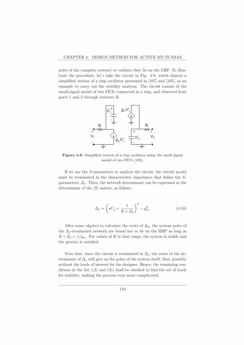
CHAPTER 4. DESIGN METHOD FOR ACTIVE-MN IN ESAS
poles of the complete system) to validate they lie on the LHP. To illus-
trate the procedure, let’s take the circuit in Fig. 4.9, which depicts a
simplified version of a ring oscillator presented in [107] and [105], as an
example to carry out the stability analysis. The circuit consist of the
small-signal model of two FETs connected in a ring, and observed from
ports 1 and 2 through resistors R.
R
V2gmV'2
R
V1
V'1
V'2
+
-
gmV'1
+
-
+
-
+
-
Figure 4.9: Simplified version of a ring oscillator using the small signal
model of two FETs [105].
If we use the S-parameters to analyze the circuit, the circuit model
must be terminated in the characteristic impedance that define the S-
parameters, Z0. Then, the network determinant can be expressed as the
determinant of the [S] matrix, as follows
Δs =
(sCg +
1
R+ Z0
)2
− g2m. (4.10)
After some algebra to calculate the roots of Δs, the system poles of
the Z0-terminated network are found not to lie on the RHP as long as
R+ Z0 < 1/gm. For values of R in that range, the system is stable and
the proviso is satisfied.
Note that, since the circuit is terminated in Z0, the roots of the de-
terminant of Δs will give us the poles of the system itself, thus, possibly
without the loads of interest for the designer. Hence, the remaining con-
ditions in the list ((2) and (3)) shall be checked to find the set of loads
for stability, making the process even more complicated.
110

4.2. AN INTEGRAL DESIGN METHOD
Furthermore, in most cases, the appropriate network determinant is
too complicated to be easily determined or factorized. Moreover, we only
want to know whether there are any RHP zeros of Δs rather than their
exact location in the complex plane. Then, it is possible to make use of
the Nyquist test. Therefore, according to the Nyquist test, by tracing the
locus of Δs as s travels clockwise around the RHP s-plane, the number
of times the locus encircles the origin, in such clockwise direction, equals
the difference between the number of zeros and poles of Δs lying on the
RHP. It is necessary to assume that the network matrix is formed by
components such that none of them have RHP poles. As a result, the
network determinant, Δs, has no RHP poles, and the number of Nyquist
encirclements indicates the number of RHP zeros —the unstable poles
of the system— [105].
Further, for convenience, instead of testing Δs, an alternative is to
evaluate the Normalized Determinant Function (NDF), first devised by
Platzker et al. in [107]. The NDF is defined as the quotient Δs/Δs0,
where Δs0 is the network determinant when all dependent sources are
turned off [108]. Since Δs0 is the determinant of a passive network, it
has no RHP zeros and, thus, it does not introduce any RHP poles to
Δs/Δs0. By normalizing the network determinant in this way, we force
Δs/Δs0 to reach 1 along the semicircular part of the s contour —in the
right-half of the s-plane— where |s| is infinite, and the circuit is assumed
passive. In consequence, Δs/Δs0 only needs to be evaluated along the
imaginary axis, s = jω. A more detailed description of these properties
are shown in Appendix A. A further theoretical discussion is presented
in [11].
Then, following the nomenclature presented in (4.9), the NDF can
be defined as (4.11) if the admittance parameters are used to describe
the system.
NDF (s) = |Y(s)| / |Y0(s)| = Δs/Δs0, (4.11)
where |Y(s)| is the determinant of the studied system, and |Y0(s)| isthe determinant of the same circuit but with all the dependent generators
(associated to active elements in the NIC) switched off. As mentioned
111

CHAPTER 4. DESIGN METHOD FOR ACTIVE-MN IN ESAS
above, it is possible to determine the number of zeros of the NDF in the
RHP as the number of encirclements of the NDF around the origin in
the complex plot. The system will be stable if the NDF does not encircle
the origin when it is evaluated from ω = −∞ to ω = ∞ [107].
The NDF can be easily calculated as (4.12) for the ring oscillator
shown in Fig. 4.9, the condition of stability has been infringed by set-
ting R + Z0 = 1.5/gm. Note that, for this example, it is easier to di-
rectly compute the roots of the network determinant by solving Δs = 0,
rather than calculate the two-stage NDF function. Nonetheless, in prac-
tical problems, where the designer is interested in including parasitics
in devices, deviations from nominal values of components, manufactur-
ing tolerances, arbitrary terminations (other than Z0), and so on, this
algebraic calculation becomes in a cumbersome —perhaps impossible—
task.
NDF =Δs
Δs0= 1− g2m
[(R+ Z0)−1 + jωCg]. (4.12)
0 1
-1
1
-1 2-2
Ā<0
Ā>0
Figure 4.10: Nyquist plot of the NDF, for the ring oscillator in Fig.
4.9, once set the relation R+ Z0 = 1.5/gm.
Figure 4.10 show the Nyquist trace of the NDF in (4.12). Since
the NDF encircles the origin, the complete circuit is unstable for that
particular terminations.
Struble and Platzker went beyond on this method in [108] and
[109], and devised an outstanding technique that takes advantage of
112

4.2. AN INTEGRAL DESIGN METHOD
EDA/CAD software to plot the Nyquist test of the NDF. Thus, by us-
ing any software for circuit analysis, it is possible to evaluate the NDF
through the called Return Ratio (RR). The concept of return ratio was
first discussed by Bode [11], and after by Maclean [110], and others [111],
and was used to assess the stability of feed-back amplifiers. This concept
can be related to the NDF of a network containing linear models of its
active devices. The RR of an active element, which is embedded into a
network, is defined as the response developed across its dependent nodes
by an external excitation of magnitude 1.
Active Network
Ip
Yp
VugmVu
ith Dependent Source
Il
(a)
Active Network
Yp
Vu
gmV'u
Independent Source
V'u
RR=-Vu/V'u
Il
ExternalSource
(b)
Figure 4.11: Sketch for the calculus of RRi where: a) the ith
dependent source is replaced for (b) an independent source of arbitrary
amplitude V ′u = 1. All others external excitations (Ip) are also removed.
To find a RR, let’s suppose a network with M active devices, all
modeled with dependent current sources, as depicted in Figs. 4.11(a and
b). First, remove all external excitations while retaining their associated
impedances (see Fig. 4.11a). Then, select one of these sources, say,
Il = gmVu, where Il is dependent on the voltage Vu. Make this source
independent by redefining it as Il = gmV ′u, where V ′
u is an external
unconnected ideal source (for convenience, of magnitude 1), as it is shown
in Fig. 4.11b. Finally, the response of the independent node, Vu, can be
evaluated leading to the RR be defined as
RR1 ≡ −Vu
V ′u
. (4.13)
This RR1 is related with the network determinant by (see Appendix
A and [11])
113
CHAPTER 4. DESIGN METHOD FOR ACTIVE-MN IN ESAS
Δs
Δs01= RR1 + 1. (4.14)
This relation is not the NDF since Δs01 is the network determinant
with just one dependent source set to zero, whereas the denominator of
the NDF, Δs0, has all sources set to zero. Δs01 may have RHP zeros,
while Δs0 has none. In order to obtain Δs0 in this process, all the
remaining RRs must be computed by maintaining the already evaluated
dependent sources turned off. Hence, the NDF can be calculated as
follows:
NDF =M∏i=1
(RRi + 1) =Δs
Δs0M=
Δs
Δs0, (4.15)
where RRi is the return ratio for the ith dependent source; M is the
total number of active elements of the network, thus, RR1 is the return
ratio of the source i = 1, when the sources i = 2, 3...M are switched on.
In the same way, RRk is the return ratio of the source i = k, when the
sources, i = 1, ..., (k − 1), are switched off.
In practical designs, the symmetry property in the NDF polar plot
around the horizontal (x ) axis, between the positive and the negative
frequencies (see Fig. 4.10) can be used for simplification of the analysis.
Such property can be expressed as the relation: NDF (−ω) = NDF ∗(ω).Thus, it is usually enough to compute NDF along the range [0, ω) only,
and afterwards, calculating the complex conjugate ofNDF (ω > 0). This
procedure allows the use of almost any type of modern circuit simulators,
and at the same time, reduces the processing time.
It is important to note that it is necessary to extract the linear model
for each active device in the non-Foster network, around its bias point,
prior to carrying out the NDF calculation. The more accurate the linear
models are the more reliable the NDF is for predicting stability. A more
detailed description of the NDF, comprising its properties and algebraic
deduction is presented in Appendix A.
114

4.2. AN INTEGRAL DESIGN METHOD
A remarkable advantage of using an EDA circuit simulator to com-
pute the NDF is the possibility of including the two-port network sub-
circuit in the same schematic containing the NIC. That sub-circuit can
be either the simulated or the measured S-parameter matrix of the ESA
whose port-2 is located in a low sensitivity position. Moreover, other pa-
rameters like package parasitics, lossy transmission lines, etc. can also
be included. This fact allows us to carry out the stability analysis of
the whole antenna system (antenna + NIC) at once, and accounting for
several parameters effects related with a realistic application.
4.2.4 Step 4: Radiation Considerations
According to the antenna structure and the selected NIC topology,
the current distributions can change, and different modes can be ex-
cited once a non-Foster network is placed. This phenomenon is more
significant for planar structures, as shown in the previous chapter. In a
linear structure, (e.g. dipoles and loops) the currents along the antenna
do not change when an ideal purely reactive implementation of ZanNIC is
placed along the antenna. Nevertheless, the resistive part of a real non-
Foster network, unavoidable in practice, will produce some changes in
the radiation pattern that must be considered in the design process.
In this sense, testing the real part of the implemented NIC impedance
is crucial. If the resistive part of the needed analytical impedance ZanNIC
(4.2), is far from zero and, at the same time, the Sens value is not low
enough, poor impedance performance can be expected in the evaluating
location of the port-2.
4.2.5 Step 5: Components’ Tolerance Effects
Additionally, and complementary to sensitivity and stability analysis,
a study about the influence of the tolerance of components (i.e. resistors,
capacitors, and inductors) in the impedance response of the NIC, and
in the stability of the antenna system is profitable. The easiest way to
do that is through a CAD circuit software with the option of statistical
analysis, in order to study the effects of possible variations on circuit per-
formance, where a confidence interval around the nominal values of each
115

CHAPTER 4. DESIGN METHOD FOR ACTIVE-MN IN ESAS
component (e.g. normal distribution for the nominal values in lumped
elements with some tolerance percentage given by the manufacturer) can
be set up. Moreover, it is possible to include parameters of the transistor
linear model, physical lengths of the layout and package parasitics.
There are two steps that must be performed before analyzing the
deviation of a circuit response, associated to the tolerance of its com-
ponents. The first step is setting up the statistical properties of each
parameter value to be analyzed. The second one is the specification of
the goals that are used to determine if the circuit has an acceptable or
unacceptable performance. Then, iterative simulations take place auto-
matically, and the results can be evaluated by graphic inspection or by
numeric calculation of the deviation from some interval of interest, e.g.
the S11 parameter over the intended bandwidth.
Figure 4.12a shows a typical graphical result of a tolerance anal-
ysis, carried out in the commercial software Applied Wave Research
(AWR)� for FET-based NII circuit, shown in Fig. 4.12b, previously
described in Section 2.7.2, when it is embedded into a small antenna. In
this example, the effects on the NDF plot are observed as the result or ap-
plying a statistical analysis —called yielding analysis in AWR— around
the nominal values of the NIC components, such as the transconductance
gm of transistors, the microstrip paths size, the DC-biasing elements, etc.
The importance of tolerance analysis does not rely on the statistic
calculation around nominal values; but in the identification of those pa-
rameters that have the most influence on the expected performance of
the whole antenna system, providing reliability and higher control for
the designer. For the case of the NII in Fig. 4.12b, a tolerance of 10%
in the analysis shows that the circuit remains stable, as the NDF plot
does not encircle de origin.
4.3 Noise Considerations
Noise can be understood as any disturbing influences on the signal
of interest. It is one of those factors that is either difficult to ana-
lyze and measure in practical applications. There is a number of noise
sources involved in any communication system, some of them are part
116

4.3. NOISE CONSIDERATIONS
(a)
ZNII
Port 1
ZL
Q1
Q2
(b)
Figure 4.12: (a) Typical tolerance analysis outcome over the NDF
computation from the MOSFET-based NII circuit sketched in (b), when
it is embedded in an ESA.
of the propagation media itself, and others are consequence of electronic
phenomena inherent to the circuitry composing the transmitters and
receivers. Among the first category of noise sources, it is worth men-
tioning those that are present in the propagation media of radio signals:
the noise in the atmosphere.
Since the atmosphere is not composed of air only, a significant in-
teraction between it and the electromagnetic radiation has been verified
throughout the development of radio communications [112]. It is possi-
ble to say that the behavior of the atmosphere against the propagation of
electromagnetic waves is determined mainly by two major components:
oxygen and water vapor. These elements show states of vibration and ro-
tation of their molecules. In turn, these states exhibit absorption peaks
corresponding to the points with greater attenuation of a wave traveling
through the atmosphere. Those peaks are located at frequencies around
24 GHz and 185 GHz, associated with the water vapor, and at 60 GHz
and 118 GHz, in the case of oxygen, as can be observed in Fig. 4.13.
Under the 3 GHz or 4 GHz, other factors come into play, such as
the atmospheric noise. This type of noise can be described as a natural
process primarily caused by lightning discharges in thunderstorms, es-
117

CHAPTER 4. DESIGN METHOD FOR ACTIVE-MN IN ESAS
Noise
Man made noise (urban)
"Big Bang"
Cosmic Noise
atmospheric noise (UK night)
Rain attenuation
Attenuation by atm. gases(at the sea level)Water vapor 7.5 g/m3
Fog0.1 g/m3
Minorcomponents
H2O
H2OO2 CO2
Specific attenuation
(dB/Km)
Noise Temperature (K)
HF VHF UHF SHF
Wavelength (Ā)
Frequency
Figure 4.13: Atmospheric noise contributions [112]. The background
intensity indicates the atmospheric opacity level.
pecially in the ionosphere, and whose influence is greater at frequencies
below 30 MHz. In this interval, the attenuation is such high that the
ionosphere can be treated as a reflector. The receiving systems designed
to operate in this frequency region are called natural-noise limited [75].
Another contribution to the noise in the atmosphere is the cosmic noise,
associated with all the astronomical bodies surrounding the earth in our
galaxy, as depicted in the right side of Fig. 4.13.
Finally, the man made noise appears as the result of all the elec-
tric machinery, hand-held devices, other radio communication systems,
among others, especially in urban areas. Summarizing, the best choice
for the propagation of electromagnetic waves through the atmosphere,
is the microwave band, thus, for wavelengths in the order of centime-
ters or tenths of a meter. At lower frequency bands, however, several
applications have been possible due to the engineering of other alterna-
tives aiming at compensating the signal degradation caused by the noise
and the low gain of the small antennas involved (repeater stations, high
power at the radiation stage, among others). It is possible to list some
of those applications as aeronautical communications (ground-to-aircraft
and aircraft-to-aircraft), Frequency Modulation (FM) broadcasting, ana-
118
4.3. NOISE CONSIDERATIONS
log television, over-the-horizon radar, TETRA links, etc. Nevertheless,
the noise and its effects are always present in the communications sys-
tems, and its analysis and measurement are of capital importance for
obtaining reliable and controlled designs.
On the other hand, internal electronic noise in transistors and resis-
tors results of physical phenomena, associated with the natural granu-
larity of charge in electronic devices. Thus, current consist of a very
large number of individual charge quanta. Hence, at the junction of a
diode, for example, the current resulting of injecting charge is not purely
constant. It still exhibits some random variations, which are called shot
noise. Also, associated with the shot noise, it has to be mentioned other
electronic noise sources: the flicker and the burst noise, also known as
the low-frequency noise forms, or the 1/f , 1/f2 noise, respectively. An-
other important source of electronic noise is due to the random motion
of charges in lossy elements, at temperatures above absolute zero. This
type of noise is called thermal noise, and as it can be predicted from fun-
damental physics principles, is used as a standard for describing other
types of noise [113].
In any case, noise has been, and continues to be, a fundamental lim-
itation to the capabilities and performance of communication systems.
In fact, information and communication theory are almost entirely for-
mulated around the problem of obtaining reliable communication in a
noisy environment.
Therefore, it is possible to describe the quality of a communication
system, especially in the receiving side, by measuring the signal-to-noise
parameter (SNR). The SNR appears as an important parameter in such
a way it describes the strength of a signal in relation to the noise ac-
companying it. The output SNR is dependent on the receiver input
SNR and the Noise Figure (NF) of the receiver chain, understood as the
degradation of the SNR between its input and output ports. Input SNR
is a function of the power transmitted, transmitter antenna gain, atmo-
spheric transmission coefficient, temperature, receiver antenna gain, and
receiver NF. The reduction of the receiver NF enhances the output SNR.
On the other hand, for cases when embedded devices are present in
the receiving chain, it is no possible to access all the points that would
119

CHAPTER 4. DESIGN METHOD FOR ACTIVE-MN IN ESAS
be of interest to measure the SNR parameter. The characterization of
the noise in a noisy device is commonly carried out by measuring its
noise figure, computed as the noise factor, F , expressed in decibels, as
follows
F =Si/Ni
So/No=
SNRi
SNRo, and
F ≥ 1,
(4.16)
NF = 10 log(F ) (dB), and
NF ≥ 0 (dB).(4.17)
That is the case when an ESA is designed to contain an active non-
Foster MN, the noise figure measurement becomes a challenging task.
Additional considerations have to be addressed in order to estimate if
the inclusion of an active MN to the antenna structure represents an
advantage or an issue for the merit NF of the global antenna system.
Thus, a primary circuital parameter should be used to estimate the SNR
degradation (or advantage). This parameter can be the figure-of-merit
G/T , where G is the antenna gain and T stands for the equivalent noise
temperature of the receiving system, as it will be described below.
In active-loaded receiving antennas, as it is the case of an ESA with
an embedded non-Foster MN, the parameter that contains all the infor-
mation on the performance of the active antenna is the figure-of-merit
G/T . This parameter remains constant along the entire receiver, and
comprises an interesting alternative when its components (G or T ) can-
not be separately measured. Thus, G/T is the only parameter that can
be directly measured by applying a conventional on–off method [114]. A
discussion on the G/T -parameter in actively loaded antennas (oscillator,
amplifier, mixer or impedance-converter types) has been made in [115]
and [116]. The underlying idea is that as the active element is directly
connected to the antenna, the losses between the active-MN and the
antenna are mainly due to the radiation efficiency. These losses can be
included in a new loss factor Le > 1. It must also be noted that the
actual actively matched antenna temperature Ta (not physically avail-
able) is not the same as the one in the passive system counterpart. Ta
depends on the overall antenna pattern which, for the actively matched
antenna, is not exactly the same as that for the passive one. The figure-
of-merit, G/T , in an actively matched antenna is then given as (4.18),
120
4.3. NOISE CONSIDERATIONS
where Fopt is the optimum noise factor, and Trec is the receiver equivalent
noise temperature.
G
T=
GACT
ΔG
Ta + T0(Le − 1) + T0(Fopt − 1)Le + T0(L− 1) · Le
ΔG·L + Trec·Le
ΔG
.
(4.18)
ΔG accounts for the potential increase in gain once the active device
is added (e.g. in the amplifier-type active antenna). For the case of
an actively matched antenna, since the non-Foster MN is not aimed at
providing power gain across its ports, ΔG should be ideally computed
as 1. Hence, in theory, once the NIC is added no insertion losses should
be expected either. T0 is the room temperature and L stands for the
losses associated to the NIC components. Finally, GACT is the effective
gain, a parameter that can result in a value larger than the directivity
of the corresponding passive (unloaded) antenna, as it is the case of
amplifier-type active antennas. For an actively matched antenna, the
maximal effective gain value is the maximal directivity itself, because
of the improvement in the overall reflection coefficient, |ΓIN| (neglectingthe ohmic losses of the radiating element), result of adding the active
MN. An expression for the effective gain, as a function of the observing
direction, is given as [114]
GACT = DMAX(θ, φ)ΔG(1− |Γ|2IN)
L, (4.19)
where L is a factor that accounts for losses in the active non-Foster
MN. Then, once measured the G/T parameter, the overall noise contri-
bution from the actively matched antenna can be extracted as in (4.20),
provided standard anechoic chamber conditions (Ta = T0).
FACT =kTACTB
kT0B
∣∣∣∣Ta=T0
= FoptLe +(L− 1)Le
LΔG, (4.20)
where TACT is the equivalent noise temperature for the system (an-
tenna + NIC). As ΔG is not large enough, the terms on the right side
in (4.20) have comparable magnitudes.
121

CHAPTER 4. DESIGN METHOD FOR ACTIVE-MN IN ESAS
For frequencies at which an anechoic chamber is not a viable op-
tion (e.g. at the VHF band), most of the authors in the reported
work —with practical implementations— have followed a conventional
on–off method [39] to characterize the noise performance in the actively
matched ESA. This method comprises two stages. First, the gain advan-
tage measurement, which accounts for the improvement in the realized
gain between the NIC-loaded ESA and the unloaded (unmatched) ESA.
The scheme of this measurement is shown in Fig. 4.14a (previously de-
scribed and depicted in Fig. 2.27b, Section 2.8). Second, the output SNR
advantage measurement, in which some additional steps are needed ac-
cording to the scheme shown in Fig. 4.14b. The complete method steps
can be listed as follows:
1. Unloaded Receiving ESA with the transmitter OFF: for measuring
the noise floor (unmatched case), N0 (dBm).
2. NIC-loaded Receiving ESA with the transmitter OFF: for measur-
ing the noise floor, N1 (dBm).
3. Unloaded Receiving ESA with the transmitter ON: for measuring
the signal level (unmatched case), S0 (dBm).
4. NIC-loaded Receiving ESA with the transmitter ON: for measuring
the signal level, S1 (dBm).
As a result of the listed procedure, the possible advantage in SNR
for the actively-loaded antenna can be computed as
SNRadv:dB = Gainadv −Noiseadded,
SNRadv:dB = (S1 − S0)− (N1 −N0). (4.21)
In addition, some analytical treatment, reported in [117], identified
the non-Foster matching approach for ESAs as advantageous for noisy
receivers only (i.e. NFreceiver > 6 dB). This, along with the simulation-
based analysis presented in [118], leads us to the assumption that the
inclusion of non-Foster elements in an antenna does not imply an obvious
advantage in the output SNR of the global system.
122
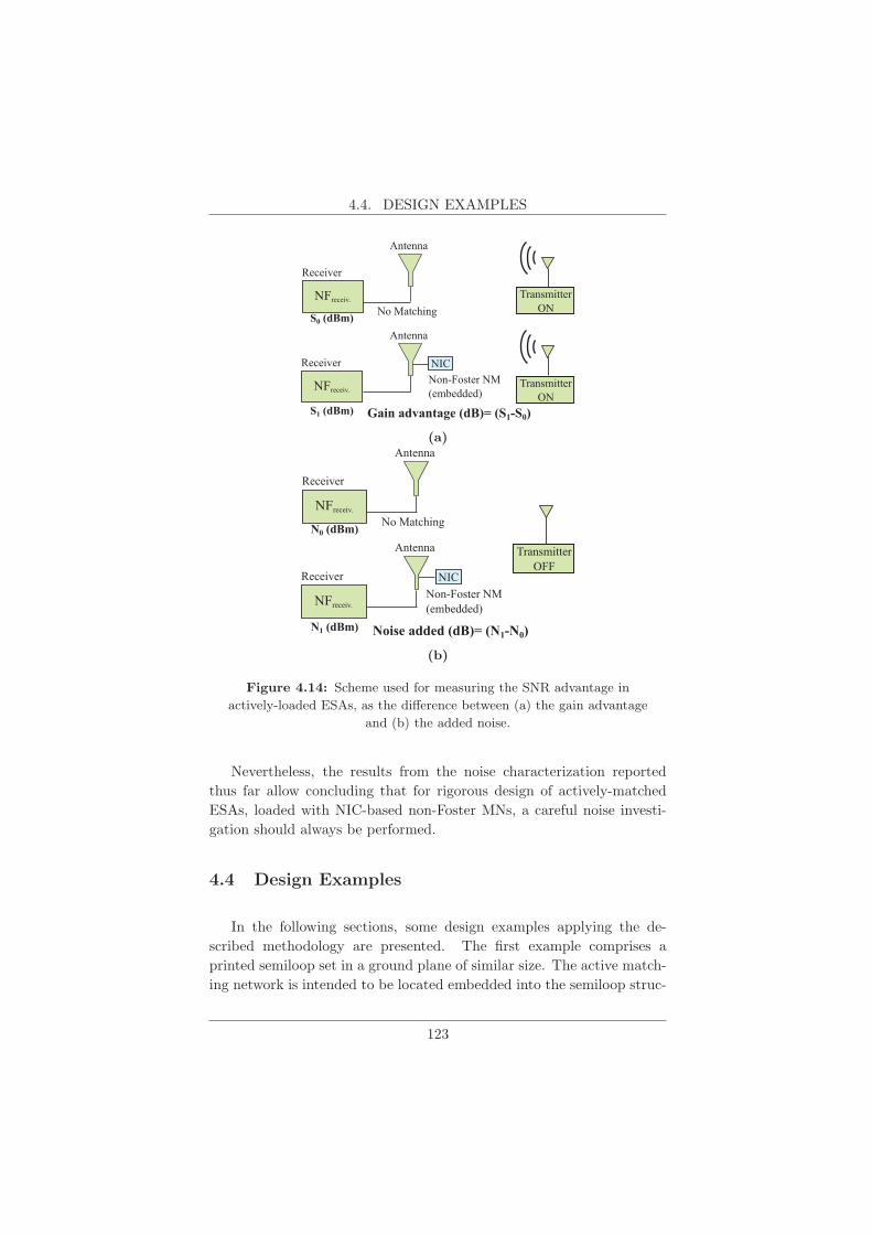
4.4. DESIGN EXAMPLES
Gain advantage (dB)= (S1-S0)
Antenna
Non-Foster NM(embedded)
TransmitterON
Antenna
No Matching NFreceiv.
S0 (dBm)
S1 (dBm)
NIC
Receiver
NFreceiv.
Receiver
TransmitterON
(a)
Noise added (dB)= (N1-N0)
TransmitterOFF
Antenna
Non-Foster NM(embedded)
Antenna
No Matching NFreceiv.
N0 (dBm)
N1 (dBm)
NIC
Receiver
NFreceiv.
Receiver
(b)
Figure 4.14: Scheme used for measuring the SNR advantage in
actively-loaded ESAs, as the difference between (a) the gain advantage
and (b) the added noise.
Nevertheless, the results from the noise characterization reported
thus far allow concluding that for rigorous design of actively-matched
ESAs, loaded with NIC-based non-Foster MNs, a careful noise investi-
gation should always be performed.
4.4 Design Examples
In the following sections, some design examples applying the de-
scribed methodology are presented. The first example comprises a
printed semiloop set in a ground plane of similar size. The active match-
ing network is intended to be located embedded into the semiloop struc-
123

CHAPTER 4. DESIGN METHOD FOR ACTIVE-MN IN ESAS
ture itself in order to set a bidirectional antenna, with an engineered
impedance bandwidth at Very High Frequency (VHF) frequencies, with-
out affecting its natural resonant band.
The second example accounts for a printed blade-type monopole,
whose natural resonant frequency is at the lower part of the Ultra High
Frequency (UHF) band, loaded with an embedded non-Foster circuit. In
this case, an impedance matching bandwidth over a frequency range in
the lower part of the VHF band is intended. The monopole is electrically
small across the interest band. The involved application is the aircraft
radio communication systems, in response to the continuous changes
and demanding requirements on aerodynamic drag in airplanes, which
implies the need for miniaturization of the antennas involved in such an
airborne systems.
4.4.1 Small Printed Semiloop Actively Matched with an
Embedded NIC
A printed small semiloop, with a radius R = 40 mm in an FR4
substrate of 0.5 mm thick, εr = 4.4, and loss tangent Tanδ = 0.02,
has been built. The objective is to obtain an impedance matched dual-
band small antenna, with a monopole-like radiation pattern at the lower
band (i.e. VHF-band up to 200 MHz) as well as a simple and low-cost
fabrication (see Fig. 4.15a).
Sensitivity Analysis
The proposed antenna is an ESA for frequencies up to 450 MHz
since the factor ka < 0.5, where a is the radius of the smallest sphere
enclosing the antenna system (1.3 ∗R in the current design) at the reso-
nance frequency, f0 = 1.2 GHz, and k is the free-space wavenumber (i.e.
k = ω0/c). The antenna and the embedded non-Foster circuit are first
modeled in a CAD full-wave simulator and in an EDA circuit simulator,
respectively, prior to be manufactured. As claimed before, according to
the proposed methodology, the first instance of the design process con-
sists of checking the suitability of this structure to be actively matched.
Thus, to obtain the Sens parameter, a sweep of the port-2 location is
124

4.4. DESIGN EXAMPLES
(a) (b)
Figure 4.15: (a) Proposed prototyped small semiloop antenna with the
embedded NIC. (b) The averaged sensitivity Sens over the antenna
structure.
made using the Computer Simulation Technology (CST)� software, by
including a gap in the semiloop at different angles to connect the analyt-
ical port-2, and extracting a two-port S-parameter matrix each time. A
region with low sensitivity (|Sens| < 10 dB) is found on the opposite side
of the input port, near to the ground plane, as depicted in Fig. 4.15b.
Sens parameter was computed as the average of (4.9) over a frequency
range from 10 to 300 MHz (VHF band).
NIC Topology and Components Selection
Since the best location is near the ground plane, a grounded NIC
topology will be easy to implement. In previous efforts, in the seeking
for alternatives to achieve stable and easy-to-build grounded NICs, a
grounded NII topology, first proposed by Kolev [67], was found. This
topology is selected as active MN for the semiloop antenna in this de-
sign example. The circuit consists of two BF998 MOSFETs connected
in the way shown in Fig. 4.17a. There is a strong dependence of ZNII
on the squared transfer-conductance (gm)2; as shown in the equation in
Fig. 4.17a. Since the NII property used here is its negative-slope reac-
tance, the terms NIC and NII can be interchanged, as mentioned before
in Chapter 2. The choice of the transistor and its bias conditions consti-
tute a trade-off between the stability of the NII and the maximum fre-
quency of non-Foster response. Increasing the working frequency implies
choosing a transistor with higher transient frequency. However, higher
transient frequencies imply higher transfer conductance, and therefore,
higher levels of feed-back currents. This fact results in potentially higher
125

CHAPTER 4. DESIGN METHOD FOR ACTIVE-MN IN ESAS
instability problems. For this reason, a transistor with a moderate tran-
sient frequency and with a stable transfer admittance, over a bandwidth
as large as possible, is welcome. The proposed transistor presents a con-
stant forward transfer admittance up to 1 GHz (see Fig. 4.16) and a
transient frequency fT = 1.9 GHz.
Figure 4.16: Forward conductance parameter vs. frequency in the
BF998 MOSFET, taken from the datasheet [119].
NIC Impedance Performance
The non-Foster behavior in the NII impedance (ZNII) should be ex-
pected at frequencies up to 200 MHz (approximately fT /10, as men-
tioned in Section 4.2.2). It is confirmed by the negative slope in the
imaginary part of the simulated NII impedance in Fig. 4.17c. The change
in the slope of the NII reactance indicates those frequencies after which
the gate-source internal capacitance, Cgs, dominates the impedance re-
sponse at the NII input port. This frequency approximately corresponds
to the maximum range of impedance matching at the added lower band,
as it will be shown below. In addition, the sharply change in slope of
ZanNIC, at frequencies above 400 MHz, makes this analytical impedance
difficult to fit even with a NIC (or a NII) working at higher frequencies,
as it can be seen in Fig. 4.17c. Thus, a practical NIC (or NII) will not
fit the required ZanNIC. This condition explains the dual-band response of
the antenna, and limits the performance of an ultra-wide-band actively
matched semiloop. A series LC -tank (LL = 15 nH, CL = 55 pF) is
126
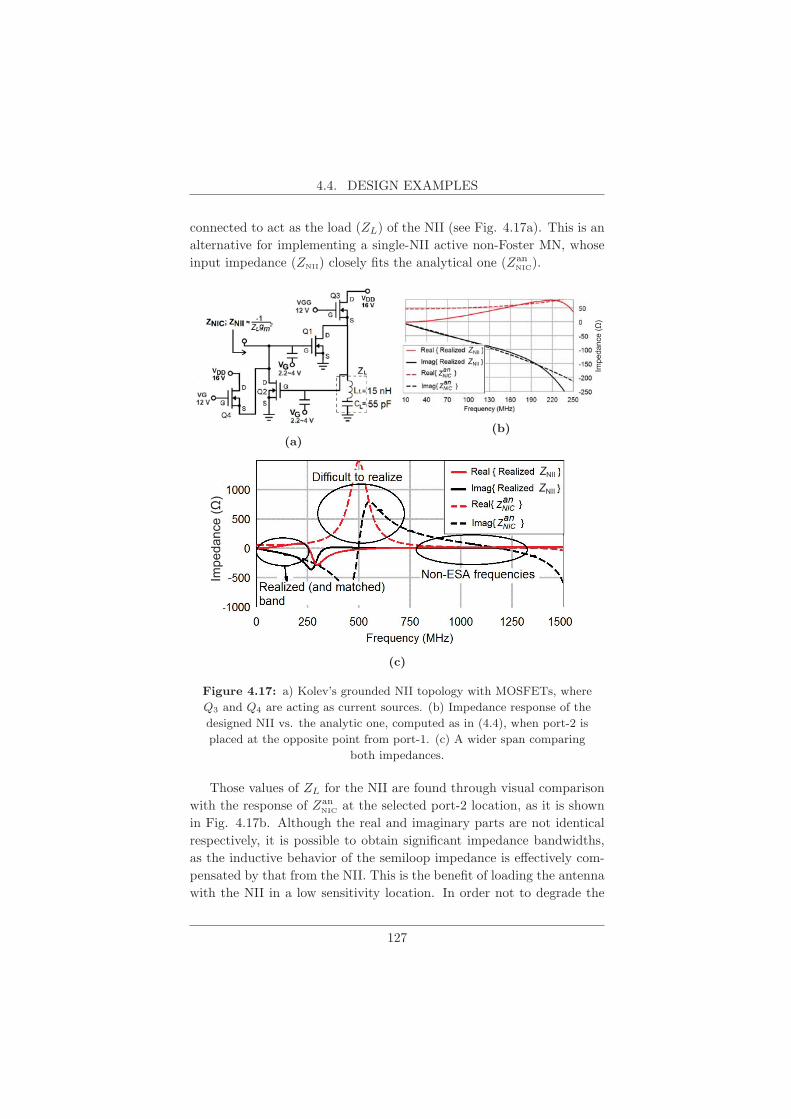
4.4. DESIGN EXAMPLES
connected to act as the load (ZL) of the NII (see Fig. 4.17a). This is an
alternative for implementing a single-NII active non-Foster MN, whose
input impedance (ZNII) closely fits the analytical one (ZanNIC).
(a)(b)
(c)
Figure 4.17: a) Kolev’s grounded NII topology with MOSFETs, where
Q3 and Q4 are acting as current sources. (b) Impedance response of the
designed NII vs. the analytic one, computed as in (4.4), when port-2 is
placed at the opposite point from port-1. (c) A wider span comparing
both impedances.
Those values of ZL for the NII are found through visual comparison
with the response of ZanNIC at the selected port-2 location, as it is shown
in Fig. 4.17b. Although the real and imaginary parts are not identical
respectively, it is possible to obtain significant impedance bandwidths,
as the inductive behavior of the semiloop impedance is effectively com-
pensated by that from the NII. This is the benefit of loading the antenna
with the NII in a low sensitivity location. In order not to degrade the
127

CHAPTER 4. DESIGN METHOD FOR ACTIVE-MN IN ESAS
radiation efficiency, a NIC circuit with a low real part (ideally zero) in its
input impedance must be connected. The bias circuit consists of another
two BF998 connected as current sources to provide the drain current to
the NII’s FETs.
Stability and Components’ Tolerance Analysis
The results, in terms of impedance matching, are shown in Fig. 4.18.
The blurred red lines indicate the effects in the S11 parameter due to
a tolerance of 10%. Over a bandwidth of 140 MHz centered at 117
MHz (i.e. FBW = 119%) an acceptable matching level is measured (i.e.
|S11| < −8 dB). The natural band of the unloaded antenna is not greatly
degraded. In terms of miniaturization, values in the range 0.04 to 0.17
for the ka-factor are reached at frequencies from 47 MHz to 187 MHz.
Figure 4.18: |S11| response for the manufactured actively matched
semiloop.
The stability test was performed using the AWR Microwave Office�suite to calculate the NDF and, at the same time, statistical analysis
with a tolerance of 10% around the nominal values for all the components
and transistor linear model parameters. The S-parameter model of the
antenna was included in the calculus of the NDF. Figure 4.19 shows
that the NDF, calculated for the whole system, does not encircle the
origin of the root-locus plane, nor for the nominal values neither for the
worst tolerance case (blurred lines). The NDF was computed within
the interval [-100, 100] GHz. Since no encirclements are observed, a
128
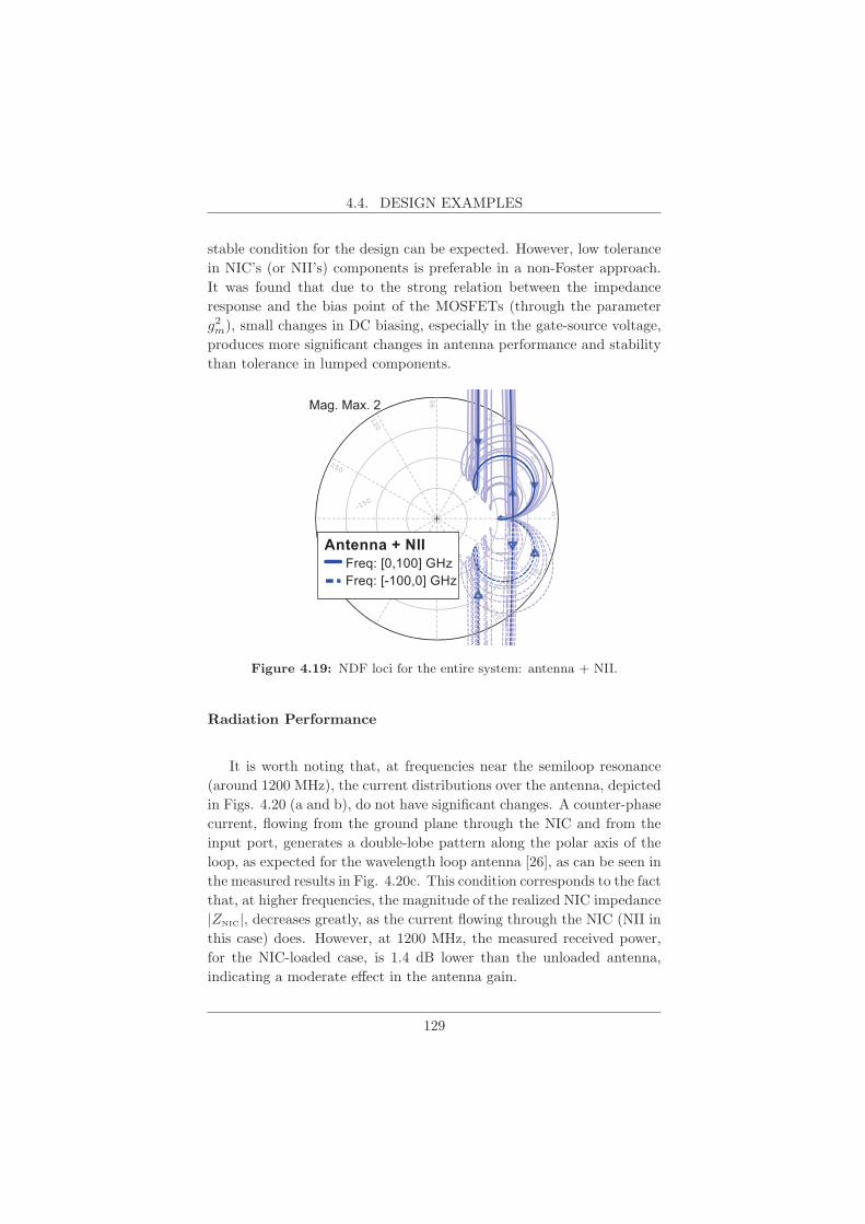
4.4. DESIGN EXAMPLES
stable condition for the design can be expected. However, low tolerance
in NIC’s (or NII’s) components is preferable in a non-Foster approach.
It was found that due to the strong relation between the impedance
response and the bias point of the MOSFETs (through the parameter
g2m), small changes in DC biasing, especially in the gate-source voltage,
produces more significant changes in antenna performance and stability
than tolerance in lumped components.
Figure 4.19: NDF loci for the entire system: antenna + NII.
Radiation Performance
It is worth noting that, at frequencies near the semiloop resonance
(around 1200 MHz), the current distributions over the antenna, depicted
in Figs. 4.20 (a and b), do not have significant changes. A counter-phase
current, flowing from the ground plane through the NIC and from the
input port, generates a double-lobe pattern along the polar axis of the
loop, as expected for the wavelength loop antenna [26], as can be seen in
the measured results in Fig. 4.20c. This condition corresponds to the fact
that, at higher frequencies, the magnitude of the realized NIC impedance
|ZNIC|, decreases greatly, as the current flowing through the NIC (NII in
this case) does. However, at 1200 MHz, the measured received power,
for the NIC-loaded case, is 1.4 dB lower than the unloaded antenna,
indicating a moderate effect in the antenna gain.
129
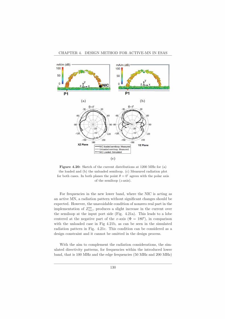
CHAPTER 4. DESIGN METHOD FOR ACTIVE-MN IN ESAS
(a) (b)
(c)
Figure 4.20: Sketch of the current distributions at 1200 MHz for (a)
the loaded and (b) the unloaded semiloop. (c) Measured radiation plot
for both cases. In both planes the point θ = 0� agrees with the polar axis
of the semiloop (z-axis).
For frequencies in the new lower band, where the NIC is acting as
an active MN, a radiation pattern without significant changes should be
expected. However, the unavoidable condition of nonzero real part in the
implementation of ZanNIC, produces a slight increase in the current over
the semiloop at the input port side (Fig. 4.21a). This leads to a lobe
centered at the negative part of the x -axis (Φ = 180�), in comparison
with the unloaded case in Fig 4.21b, as can be seen in the simulated
radiation pattern in Fig. 4.21c. This condition can be considered as a
design constraint and it cannot be omitted in the design process.
With the aim to complement the radiation considerations, the sim-
ulated directivity patterns, for frequencies within the introduced lower
band, that is 100 MHz and the edge frequencies (50 MHz and 200 MHz)
130
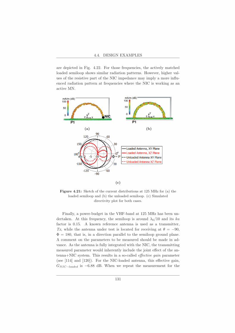
4.4. DESIGN EXAMPLES
are depicted in Fig. 4.22. For those frequencies, the actively matched
loaded semiloop shows similar radiation patterns. However, higher val-
ues of the resistive part of the NIC impedance may imply a more influ-
enced radiation pattern at frequencies where the NIC is working as an
active MN.
(a) (b)
(c)
Figure 4.21: Sketch of the current distributions at 125 MHz for (a) the
loaded semiloop and (b) the unloaded semiloop. (c) Simulated
directivity plot for both cases.
Finally, a power-budget in the VHF-band at 125 MHz has been un-
dertaken. At this frequency, the semiloop is around λ0/10 and its ka
factor is 0.15. A known reference antenna is used as a transmitter,
Tx, while the antenna under test is located for receiving at θ = −90,
Φ = 180, that is, in a direction parallel to the semiloop ground plane.
A comment on the parameters to be measured should be made in ad-
vance. As the antenna is fully integrated with the NIC, the transmitting
measured parameter would inherently include the joint effect of the an-
tenna+NIC system. This results in a so-called effective gain parameter
(see [114] and [120]). For the NIC-loaded antenna, this effective gain,
GNIC−loaded is −6.88 dB. When we repeat the measurement for the
131
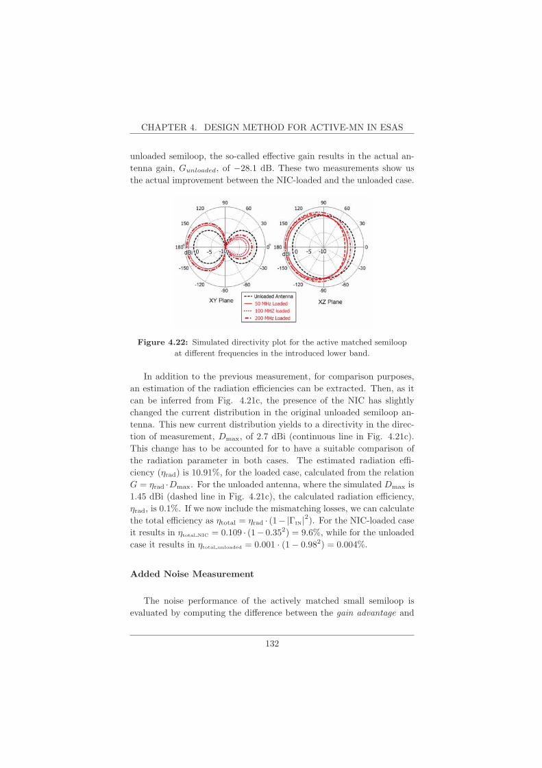
CHAPTER 4. DESIGN METHOD FOR ACTIVE-MN IN ESAS
unloaded semiloop, the so-called effective gain results in the actual an-
tenna gain, Gunloaded, of −28.1 dB. These two measurements show us
the actual improvement between the NIC-loaded and the unloaded case.
Figure 4.22: Simulated directivity plot for the active matched semiloop
at different frequencies in the introduced lower band.
In addition to the previous measurement, for comparison purposes,
an estimation of the radiation efficiencies can be extracted. Then, as it
can be inferred from Fig. 4.21c, the presence of the NIC has slightly
changed the current distribution in the original unloaded semiloop an-
tenna. This new current distribution yields to a directivity in the direc-
tion of measurement, Dmax, of 2.7 dBi (continuous line in Fig. 4.21c).
This change has to be accounted for to have a suitable comparison of
the radiation parameter in both cases. The estimated radiation effi-
ciency (ηrad) is 10.91%, for the loaded case, calculated from the relation
G = ηrad ·Dmax. For the unloaded antenna, where the simulated Dmax is
1.45 dBi (dashed line in Fig. 4.21c), the calculated radiation efficiency,
ηrad, is 0.1%. If we now include the mismatching losses, we can calculate
the total efficiency as ηtotal = ηrad · (1−|ΓIN|2). For the NIC-loaded case
it results in ηtotal NIC = 0.109 · (1− 0.352) = 9.6%, while for the unloaded
case it results in ηtotal unloaded = 0.001 · (1− 0.982) = 0.004%.
Added Noise Measurement
The noise performance of the actively matched small semiloop is
evaluated by computing the difference between the gain advantage and
132

4.4. DESIGN EXAMPLES
the added noise quantities, according to (4.21). The measurement proce-
dure described in Fig. 4.14 is set up for measuring the noise performance
of the NIC-loaded antenna, with respect to the same antenna without
any impedance matching. The transmitter comprises a signal generator,
whose output impedance is 50 Ω, driving a 60 cm height blade-monopole,
working across the upper VHF band (from 100 to 300 MHz), set over
a ground plane of 1 m side. The receiver consist of the Antenna Under
Test (AUT) —either the NIC-loaded and the unloaded semiloop— fol-
lowed by the Spectrum Analyzer (SA), the Agilent N1996A. In order to
reduce the noise figure of the instrument, and hence its sensitivity, an
external preamplifier is used (Agilet LNA-87405B), whose gain and NF
are 26 dB and 3 dB, respectively. The experiment was conducted from
110 MHz to 250 MHz.
110 120 130 140 150 160 170 180 190 2005
10
15
20
25
30 NFSA= 35 dB
SN
Rad
v (dB
)
Frequency (MHz)
SNRadv_dB=(S1-S0)-(N1-N0)
(a)
Frequency (MHz)
SN
Rad
v (dB
)
NFSA= 13 dB
SNRadv_dB=(S1-S0)-(N1-N0)
(b)
Figure 4.23: Added noise of the actively matched small semiloop,
measured as the SNRadv according to (4.21), with respect to the
unloaded semiloop. (a) For a NF SA = 38 dB (no preamp). (b) For a
NF SA = 13 dB (with the Agilent 87405B preamp).
The obtained SNRadv is depicted in Fig. 4.23, for two different noise
figures at the receiver, NF SA, depending on whether the preamplifier was
used or not. The red points represents the calculated SNRadv while the
curves corresponds to an interpolation made in the post-processing stage.
It can be observed that the NIC-loaded semiloop effectively enhances the
output SNR for a noisy receiver, as it is the case shown in Fig. 4.23a.
For a less noisy receiver, as with the reduced-NF instrument situation,
the actively matched antenna shows a SNR improvement only at certain
frequencies, especially those above 190 MHz, where the active MN does
not match the semiloop anymore (see Fig. 4.18). Additional parameters
regarding the active devices involved (i.e. the MOSFETs) such as its
biasing levels and topology should be considered in an optimization pro-
133

CHAPTER 4. DESIGN METHOD FOR ACTIVE-MN IN ESAS
cess, comprising a future line of work in active non-Foster MNs applied
to antennas.
4.4.2 Blade-type Monopole Actively Matched with an
Embedded NIC
In this section, a blade-type small monopole of 22 cm by 25 cm over a
substrate of 1.6 mm thick, and a permittivity εr = 4.35, is matched over
a 50-90 MHz range using an active non-Foster MN in two different con-
figurations: floating-MN and grounded-MN. At the frequency interval of
design, the ka factor is within 0.26 and 0.47 if the image of the monopole
(beneath the ground plate) is accounted in the computation of the radius
a. To alleviate the highly reactive response of the monopole impedance
at lower impedances, a rectangular slot is placed along the blade (see
inset sketch in Fig. 4.24), to give a longer path for currents, thus, an
inductive compensation. This response is confirmed by simulation, as
depicted in Fig. 4.24.
10 MHz500 MHz
Normal blade, 50 MHz to 90 MHz.Slotted blade, 50 MHz to 90 MHz.
Figure 4.24: Antenna impedance response, in the Smith chart, of a 25
cm by 22 cm blade monopole. The inclusion of the longitudinal slot
slightly compensates the reactive nature of the normal monopole, as the
50 to 90 MHz range is closer to the horizontal axis.
134

4.4. DESIGN EXAMPLES
The intended impedance matching level is such that |S11| < −6 dB.
The design strategy developed along this chapter is applied. Therefore,
the Sens parameter is used to find out two capital answers at the starting
point of the design. First, the confirmation of the suitability of a blade-
type monopole to be matched with an active embedded non-Foster MN
and, second, only in the case of an affirmative outcome in the sensitivity
analysis, to find out the best location for the active matching network
over the monopole structure itself, through the sensitivity analysis.
Sensitivity analysis
The first studied configuration is the grounded one. Then, once an
analytical port-2 is inserted in the antenna, through a CAD software
for full wave simulation, a sufficient number of locations for the port-2
should be set, all over the monopole structure, for extracting the same
number of S-parameters matrices. It is worth noting that in all the
situations, in the grounded configuration, the port-2 is grounded. Then,
by computing the Sens parameter applying (4.1), it is possible to plot
the behavior of the frequency-averaged Sens. The sweep result shows
the bottom corner area as the lowest sensitivity point, as it is shown
in Fig. 4.25. This is the most feasible point to connect the non-Foster
matching network.
Figure 4.25: Sens parameter over the monopole structure, averaged
from 10 MHz to 500 MHz, for the grounded-MN configuration.
135

CHAPTER 4. DESIGN METHOD FOR ACTIVE-MN IN ESAS
In order to find alternatives for a variety of NIC topologies, a floating
configuration for the port-2 is explored. In this sense, a gap in the blade
is inserted to place the port-2 and to analyze the Sens parameter. The
frequency-averaged magnitude of Sens for the floating case is depicted
in Fig. 4.26. The averaged Sens shows again the central bottom corner
area as the point of lowest sensitivity. However, the averaged Sens does
not let us to observe how the behavior of this parameter over a specific
frequency range is, in this case, for frequencies lower than 90 MHz. In
other words, once the variation of the Sens parameter over the structure
is checked, its behavior in the frequency domain, at a certain point, must
be observed.
Figure 4.26: Sens parameter over the monopole structure, averaged
from 10 MHz to 500 MHz, for the floating-MN configuration.
For the blade-type monopole, an important difference in the Sens
parameter for both floating and grounded configurations is identified
and shown in Fig. 4.27. The curves are depicted for the same frequency
interval as the one used to compute the Sens parameter in the structure-
based sweet, in Figs. 4.25 and 4.26.
Since the difference in the Sens parameter for both floating-MN and
grounded-MN configurations is over than 25 dB, within the design in-
terval (see Fig. 4.27), an important difference is expected between the
impedance matching performance obtained by certain active non-Foster
network connected at port-2, in each case. Even small differences be-
tween the realized (ZNIC) and the analytical (Zan
NIC) impedances will result
136

4.4. DESIGN EXAMPLES
Figure 4.27: Sens parameter vs frequency in a blade-type printed
monopole for two different configurations: floating MN and Grounded
MN.
in greatly narrowed lower band. The obtained impedance bandwidth for
the grounded-MN case is going to be much wider than the floating case,
as it will be shown later.
Once the lowest Sens point and the most suitable configuration have
been found, the analytical impedance, ZanNIC, derived from the ideal Γan
NIC,
can be computed as (4.2) for the S-parameter matrix extracted when the
port-2 is located in that position (the lowest Sens point). The continuous
lines in Fig. 4.28 show the real and the imaginary parts of the analytical
ZanNIC, for the grounded-MN case.
The behavior and the negative slope with frequency of the imaginary
part of ZanNIC (Xan
NIC), which indicates the non-Foster behavior needed to
be fulfilled with the MN, also gives us an idea of what kind of load
impedance we have to convert with the NIC (or the NII). In this case,
since the analytical reactance reaches negative values over an almost
straight line “going down”, in the frequency range of interest, the more
agreeable MN would be an ideal negative inductor, connected between
the monopole and its ground plane, in shunt with the feeding port.
137
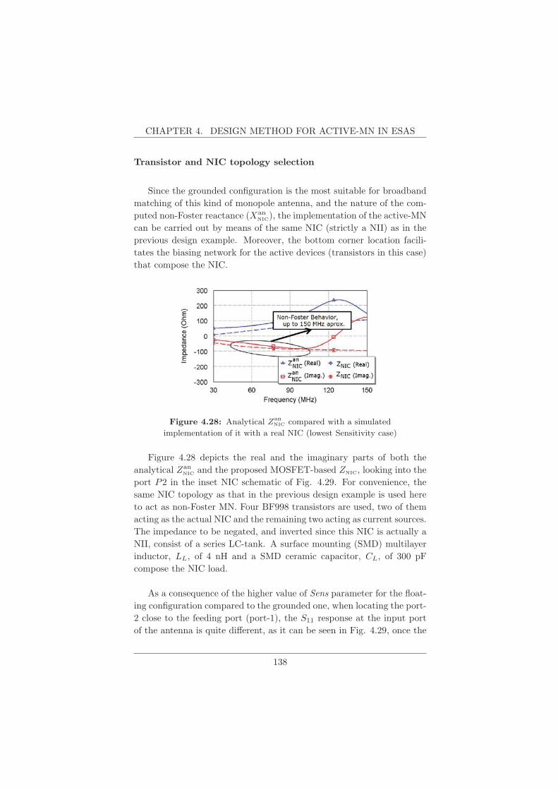
CHAPTER 4. DESIGN METHOD FOR ACTIVE-MN IN ESAS
Transistor and NIC topology selection
Since the grounded configuration is the most suitable for broadband
matching of this kind of monopole antenna, and the nature of the com-
puted non-Foster reactance (XanNIC), the implementation of the active-MN
can be carried out by means of the same NIC (strictly a NII) as in the
previous design example. Moreover, the bottom corner location facili-
tates the biasing network for the active devices (transistors in this case)
that compose the NIC.
Figure 4.28: Analytical ZanNIC compared with a simulated
implementation of it with a real NIC (lowest Sensitivity case)
Figure 4.28 depicts the real and the imaginary parts of both the
analytical ZanNIC and the proposed MOSFET-based ZNIC, looking into the
port P2 in the inset NIC schematic of Fig. 4.29. For convenience, the
same NIC topology as that in the previous design example is used here
to act as non-Foster MN. Four BF998 transistors are used, two of them
acting as the actual NIC and the remaining two acting as current sources.
The impedance to be negated, and inverted since this NIC is actually a
NII, consist of a series LC-tank. A surface mounting (SMD) multilayer
inductor, LL, of 4 nH and a SMD ceramic capacitor, CL, of 300 pF
compose the NIC load.
As a consequence of the higher value of Sens parameter for the float-
ing configuration compared to the grounded one, when locating the port-
2 close to the feeding port (port-1), the S11 response at the input port
of the antenna is quite different, as it can be seen in Fig. 4.29, once the
138
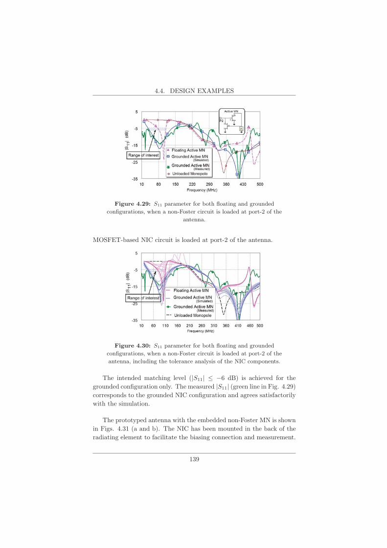
4.4. DESIGN EXAMPLES
Figure 4.29: S11 parameter for both floating and grounded
configurations, when a non-Foster circuit is loaded at port-2 of the
antenna.
MOSFET-based NIC circuit is loaded at port-2 of the antenna.
Figure 4.30: S11 parameter for both floating and grounded
configurations, when a non-Foster circuit is loaded at port-2 of the
antenna, including the tolerance analysis of the NIC components.
The intended matching level (|S11| ≤ −6 dB) is achieved for the
grounded configuration only. The measured |S11| (green line in Fig. 4.29)
corresponds to the grounded NIC configuration and agrees satisfactorily
with the simulation.
The prototyped antenna with the embedded non-Foster MN is shown
in Figs. 4.31 (a and b). The NIC has been mounted in the back of the
radiating element to facilitate the biasing connection and measurement.
139

CHAPTER 4. DESIGN METHOD FOR ACTIVE-MN IN ESAS
(a)
(b)
Figure 4.31: Prototyped antenna with the embedded non-Foster MN.
(a) Frontal view. (b) Rear view of the actively matched blade-monopole,
mounted on a 1 m X 1 m ground plate for S11 measurement.
Stability Analysis
The stability is also checked, by applying the NDF for the whole an-
tenna system (blade-monopole + NIC). Thus, the influence of the two-
port antenna (through its simulated or measured S-parameters) and all
the components in the active-MN are considered. With the aim of ob-
serving the robustness of the design, the component’s tolerance analysis
tool, available in AWR� circuit simulator, is also computed besides the
NDF. Two different percentages of tolerance are shown in Figs. 4.32a
140

4.4. DESIGN EXAMPLES
and 4.32b, both of them following a normal distribution of probability.
(a) (b)
Figure 4.32: Polar plot of the NDF computed to check the stability of
the NIC-loaded blade-monopole, in grounded configuration, for a
component tolerance of (a) 10% and (b) 15%.
The risk of instabilities increases as the tolerance in components and
microstrip paths do. Thus, it is desirable to choose low tolerance SMD
elements as well as high resolution manufacturing process to implement
the embedded active-MN. Such risk is deduced, in this case, from how
much the NDF curve gets close to the polar origin, according to the
NDF theory mentioned above and described in Appendix A. The NDF
is computed up to 100 GHz, for both tolerances, along with its corre-
spondent values for the negative frequencies (ω < 0). It is observed no
origin encirclements (i.e. the instabilities of the system) for the 10%
tolerance. However, a potential risk of instability can be expected if the
tolerance reaches 15%.
Passive vs. Active Impedance Matching Exploration
A typical question that arises from the active matching design for
ESAs is if there is no way to obtain a similar impedance bandwidth
by connecting a passive-MN, instead of an active one. In this sense, a
passive MN based on lumped-reactive elements is designed and optimized
141

CHAPTER 4. DESIGN METHOD FOR ACTIVE-MN IN ESAS
through the AWR circuit simulator software, to match the blade-type
monopole along the intended frequency band. The passive-MN comprises
two L-sections, composed of two capacitors in series and two inductors in
shunt, as depicted in Fig. 4.33. The result of connecting such a passive-
reactive network to the feed point of the antenna is depicted in 4.34,
in terms of the |S11| magnitude, and compared with the grounded-NIC
selected for this design.
Figure 4.33: Schematic of the passive-MN, connected to a measured
S11 parameter block from the one-port unloaded blade-monopole.
Figure 4.34: Passive MN vs. active MN (grounded configuration).
It can be seen the advantage that the active MN represent, even over a
automatically optimized passive MN by a simulator. Nonetheless, in real
applications, an important miniaturization level in ESAs is performed
by adding toroidal coils with ferrites cores to match the antenna [121].
This approach is widely used in airborne antennas, at the expense of
weight increase and gain reduction, this latter associated with losses in
142

4.4. DESIGN EXAMPLES
ferrites at radiofrequency (RF) bands, that is, at VHF or higher.
Radiation considerations
When loading an ESA with any kind of circuit, composed well of
lumped elements well of distributed ones, some change in the current
distribution is expected, and therefore, some change in the radiation
pattern or the radiated power has to be checked. By means of full wave
simulation, it is possible to observe the current distributions for the
antenna when loaded with the NIC acting as the active-MN. Figure 4.35
shows the current distributions for the NIC-loaded blade-type monopole,
working at 50 MHz.
Figure 4.35: Current distributions for the actively matched monopole,
at 50 MHz.
As expected, and according to the considerations discussed in Chap-
ter 3, in antennas with planar structures, there is a substantial change in
the net current distribution along the antenna, when the NIC is inserted,
in comparison when there is no NIC (unloaded one-Port antenna). In
this way, changes in the radiation pattern are expected and have to be
considered in every situation of the application.
For comparison purposes, the current distributions of the same
monopole, but without non-Foster MN (unloaded case), is depicted in
Fig. 4.36. In this case, the intensity of the current is clearly higher in
the bottom edge of the monopole, as the strength of the arrows shows.
143
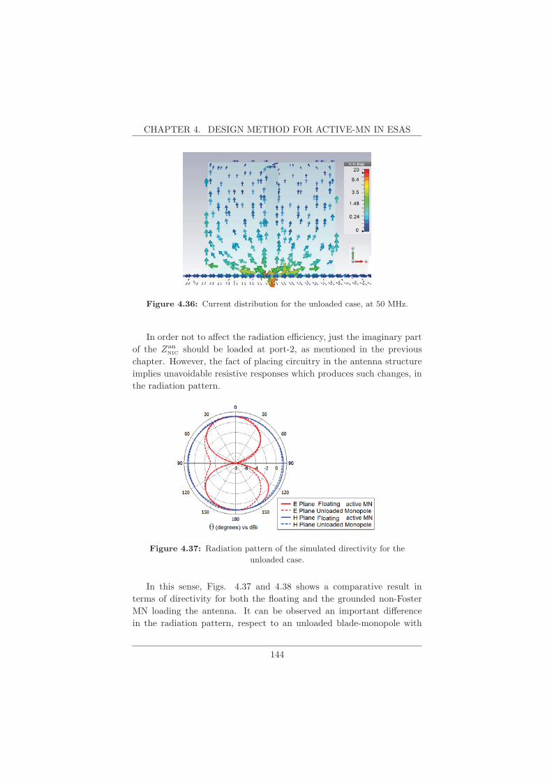
CHAPTER 4. DESIGN METHOD FOR ACTIVE-MN IN ESAS
Figure 4.36: Current distribution for the unloaded case, at 50 MHz.
In order not to affect the radiation efficiency, just the imaginary part
of the ZanNIC should be loaded at port-2, as mentioned in the previous
chapter. However, the fact of placing circuitry in the antenna structure
implies unavoidable resistive responses which produces such changes, in
the radiation pattern.
Figure 4.37: Radiation pattern of the simulated directivity for the
unloaded case.
In this sense, Figs. 4.37 and 4.38 shows a comparative result in
terms of directivity for both the floating and the grounded non-Foster
MN loading the antenna. It can be observed an important difference
in the radiation pattern, respect to an unloaded blade-monopole with
144

4.4. DESIGN EXAMPLES
Figure 4.38: Radiation pattern of the simulated directivity for the
NIC-loaded case.
its structure slotted in the same way. The grounded-MN configuration
changes the current distribution in a way that the radiation response is
a directional pattern with the main lobe perpendicular to the ground
plane. This radiation pattern differs substantially with respect to the
monopole-like pattern in the floating-MN case.
For a better understanding of the radiation effects of loading
the monopole with a grounded NIC, with non-zero resistive part
(Re{ZNIC} = 0), the 3D-plot of the directivity pattern is shown in Figs.
4.39a and 4.39b. Unquestionably, there is an important change in the
radiation response when the blade-monopole is loaded with an active
non-Foster MN, for frequencies at which the host antenna behaves as an
ESA. This changes are intimately related with the resistive part of the
NIC impedance, even when some compensation is used to reduce the
NIC resistive part, which is usually made by means of inductors and re-
sistors connected in the feedback branches of the NIC. As the radiation
resistance of an ESA is of the order of some ohms, it is possible to state
that any small resistive part in the connected MN affects not only the
radiation efficiency (by applying (2.33)) but also the radiation pattern,
in such a way that a different mode can be radiated.
Finally, and similarly to the previous design example, a power-budget
in the VHF-band at 110 MHz has been undertaken to avoid the FM
broadcasting band. A known reference antenna is used as a transmitter,
145

CHAPTER 4. DESIGN METHOD FOR ACTIVE-MN IN ESAS
(a)
(b)
Figure 4.39: Simulated 3D directivity pattern, at 90 MHz for the
blade-monopole when it is (a) loaded with the designed ZNIC, and (b) a
conventional unloaded one-port ESA.
Tx, while the antenna under test is located for receiving at θ = −90,
Φ = 180, that is, in a direction parallel to the blade-monopole ground
plane, and on the opposite side of the NIC. As the antenna is fully
integrated with the NIC, the transmitting measured parameter would
inherently include the joint effect of the antenna+NIC system. This
results in a so-called effective gain parameter (see [114] and [120]). For
146

4.5. CONCLUSION
the NIC-loaded antenna, this effective gain, GNIC-loaded is−1.24 dB. When
we repeat the measurement for the unloaded blade-monopole, the so-
called effective gain results in the actual antenna gain, Gunloaded, of−6.46
dB. These two measurements show us the actual improvement between
the NIC-loaded and the unloaded case, at least for the direction of the
expected higher directivity.
4.5 Conclusion
In this chapter, a design methodology for actively matched ESAs,
with some additional criteria to the conventional process has been pro-
posed and described. With the purpose of complementing the sensitivity
analysis presented in the Chapter 3, which aims at locating, in a smart
an automated way, the most suitable location for an active non-Foster
MN in the radiating structure. Then, by means of two different de-
sign examples, the steps of the methodology have been explained and
illustrated.
It is worth pointing out that any antenna structure can be studied
under this strategy previously to be prototyped, saving time and effort.
Antennas that are not electrically small can also be designed following
the proposed strategy. Additionally, considerations about tolerance in
components have been shown to be profitable to identify sensitive pa-
rameters, not only in lumped components values but in manufacturing
and set-up stages in the antenna plus MN system, which are studied as
a unique entity. The NDF has been used to complement the methodol-
ogy with a remarkable and easy to calculate alternative to predict the
stability of the whole antenna system.
On the other hand, in terms of radiation performance considera-
tions —one of the most challenging topics in embedded active matching
design— important changes in the radiation pattern have been found.
There are unavoidable responses in real non-Foster networks that pro-
duce changes in the current distributions, worthy of consideration, with
respect to the case of the single-port unloaded antenna. In general,
the directivity pattern, which is expected to be omnidirectional in some
plane —depending on the nature of the ESA: electric or magnetic— re-
sults in a more directive pattern, especially in the direction opposite to
147
CHAPTER 4. DESIGN METHOD FOR ACTIVE-MN IN ESAS
the point where the NIC is connected. Understood as a non-controllable
condition, this fact can be seen as a drawback if the application requires
an omnidirectional actively-matched ESA. However, in a different sce-
nario, those changes have simply to be taken into consideration in order
to reach some other application specifications.
The added noise in a receiving NIC-loaded semiloop, while good in
a noisy receiver, was found to be an issue when a low-noise receiver is
involved, as the SNRadv resulted negative, at some frequencies in the
lower band, with respect to the unloaded-unmatched case. These results
agree with the analytical ones presented in [117]. This fact suggest that
the internal noise of the NFC should be minimalized by optimizing well
the biasing topology well the biasing levels.
The improvement in the antenna effective gain is the more remark-
able advantage, in terms or radiation performance. As it was measured in
both design examples, the NIC-loaded ESA overcome their passive coun-
terpart, in 21 dB for the semiloop and 6.3 dB for the blade-monopole.
In both cases, the receiving angle agreed with the region of greater di-
rectivity, for the NIC-loaded antenna case.
148

CHAPTER 5
NON-FOSTER NETWORKS IN ANTENNAARRAYS
Once the performance of individual radiating structures (single
ESAs) when loaded with non-Foster networks for impedance matching
has been described, it is interesting to observe the response of multi-
ple radiators —an antenna array— under the same approach. First, a
brief introduction to the antenna array theory is presented and, then,
the active non-Foster impedance matching technique applied to simple
antenna arrays is presented.
5.1 Antenna Arrays Basics
Since there is no ability to control the radiation patterns of the in-
dividual element antennas, an alternative arises as combining the out-
puts of multiple antenna elements. This widely studied approach allows
us to significantly change the pattern, including pattern adjustment in
response to time changing requirements, or the overall gain in the ra-
diator [25]. In general, an antenna array, often called a phased array,
can be defined as a set of N antennas spatially separated, designed to
improve one or more performance characteristics of a radiating element.
In other words, an antenna array can be used to:

CHAPTER 5. NON-FOSTER IN ARRAYS
increase the overall gain
provide diversity reception
cancel out interference from given directions
“steer” the radiation pattern of the array to make it more sensitive
in a particular direction
determine the direction of arrival of incoming signals (scanning)
to maximize the Signal to Interference plus Noise Ratio (SINR)
According to the geometric arrangement of the elements in space,
an antenna array can be classified in three different types: linear array,
planar array, and conformal array. In a linear array, the elements are
arranged on a straight line in one dimension. The planar array presents
its elements arranged on a plane in two dimensions (rectangular, square
or circular aperture). Finally, in the conformal array the elements are
distributed on a non-planar surface (conical, semi-spherical, etc.).
The basic antenna array model consists of two parts: the element
pattern, the pattern of one of the elements, when isolated, and the array
factor, the pattern of the array with the actual elements replaced with
isotropic sources. Figure 5.1 shows a linear array with isotropic sources
equally spaced along the z-axis. The individual element behaves identi-
cally in response to a plane wave coming from any direction. However,
when this plane wave is received by the array and coupled to a common
receiver, the global isotropic array response will show constructive and
destructive interference at certain directions. Thus, the array pattern
will be a function of the angle, θ, which is the angle with respect to the
line of elements [25].
Then, the array factor can be understood as a representation of the
directivity response of an antenna array, only due to the spatial dis-
tribution of the elements and its excitation (magnitude and relative
phase) [122]. It can be computed as
AF (Ψ) =N−1∑n=0
An · ejnΨ, (5.1)
150

5.1. ANTENNA ARRAYS BASICS
Figure 5.1: Linear array of equally spaced isotropic point sources [25].
defining
Ψ = kd cos θ + α, (5.2)
where N is the number of elements, d is the distance between them,
k is the wavenumber (2π/λ), An is the amplitude factor, and α is the
phase difference between the excitation of adjacent elements. When the
elements are fixed positioned, An and α are the parameters modified by
the designer to steer the main lobe of the array. The array factor is a
function of Ψ and can be understood as a Fourier series. Note that Ψ is
an electrical and a spatial variable at the same time.
Actual arrays have radiating elements that, of course, are not
isotropic. These elements may have a different orientation, current dis-
tributions, amplitudes and relative phases with respect to each other. In
practical arrays, for the sake of simplicity in design and analysis stages,
the elements are chosen to be similar, meaning that the currents of each
element are in the same direction, of the same length, and have the same
distribution. There may be different current amplitudes and phases for
each element, to keep control on the beamforming property of the array.
This fact allows the total array pattern to be written as a product of
a single element antenna (the element pattern), ga(θ, φ), and an array
factor, f(θ, φ) (i.e. a normalized version of (5.1)). The process of factor-
ing the pattern of an array into an element pattern and an array factor
is referred to as the principle of pattern multiplication [25]. Then, the
complete pattern of an array is
151

CHAPTER 5. NON-FOSTER IN ARRAYS
F (θ, φ) = ga(θ, φ)f(θ, φ). (5.3)
Mutual Coupling
So far, the arrays have been treated as an arrangement of non inter-
acting elements being perfectly matched in impedance to the feed points.
This fact allows further assumptions: the element terminal currents are
proportional to their incident signals, the relative current distributions
on each element of the array are identical (although their levels can
be different), and finally, the pattern multiplication is valid [25]. As
expected, in a real array the elements interact with each other and al-
ter the currents (and thus impedances) from that which would exist if
the elements were isolated. This interaction, called mutual coupling,
changes the current magnitude, phase, and distribution on each element
from their free-space values. As a consequence, the total array pattern
changes in comparison to the no-coupling approach. Furthermore, these
changes are functions of the frequency and the scan angle, as it will be
described later.
The three mechanisms responsible for mutual coupling are depicted
in Fig. 5.2a. First, the direct space coupling occurs between array ele-
ments. Second, indirect coupling can occur by scattering from adjacent
elements. Third, the feed network interconnecting the elements leads to
additional coupling path. This last contribution to the mutual coupling
is mitigated by means of proper impedance matching networks (MNs)
at each element. It is possible to model each element in the array as an
independent voltage generator with its terminal impedance, the impe-
dance of the actual element and the resulting current through them, as
depicted in Fig. 5.2b [25]. V gm and Zg
m represent the voltage generator
at the mth element. The voltage and current at the element terminals,
Vm and Im, include all coupling effects. Then, an array of N elements
can be treated as an N -port network using conventional circuit analysis,
as follows:
152
5.1. ANTENNA ARRAYS BASICS
(a)
(b)
Figure 5.2: (a) Mechanisms that contribute to mutual coupling in an
array. (b) Independent voltage generator model of the mth element,
proposed in [25].
⎡⎢⎢⎢⎢⎢⎣V1
V2
...
VN
⎤⎥⎥⎥⎥⎥⎦ =
⎡⎢⎢⎢⎢⎢⎣Z11 Z12 · · · Z1N
Z12 Z22 · · · Z2N
...
Z1N Z2N · · · ZNN
⎤⎥⎥⎥⎥⎥⎦ ·
⎡⎢⎢⎢⎢⎢⎣I1
I2...
IN
⎤⎥⎥⎥⎥⎥⎦ (5.4)
where Vn and In are the voltage and current across the nth element.
Znn is the self-impedance of the nth element when all other elements
are open-circuited. Thus, the mutual impedance, Zmn (=Znm by reci-
procity) between the two terminal pairs of elements m and n is the open
circuit voltage produced at the first terminal pair divided by the current
supplied to the second when all other terminals are open-circuited; that
is,
153

CHAPTER 5. NON-FOSTER IN ARRAYS
Zmn =Vm
In
∣∣∣∣Ii=0
for all i = n. (5.5)
Mutual coupling in arrays can be described by means of some general
trends, that can be listed as follows [25,123]:
The magnitude of mutual impedance decreases with spacing dis-
tance d, in many cases decaying as 1/d2 [124].
The far field pattern is an indicator of coupling between elements,
although the coupling mechanism is a near-field, not far-field, ef-
fect. Coupling is proportional to the element pattern level in the
array plane (or surface).
Elements with a narrow pattern will have lower coupling than a
elements with a broad beam.
Elements with polarizations (i.e. electric field orientations) that
are parallel couple more than when collinear.
Larger elements have smaller coupling.
An additional way to quantify coupled arrays, in addition to the mu-
tual impedance analysis, is by using the S-parameters matrix describing
the array as an N -port network. As the S-parameters are commonly
used in full-wave simulations, and measured in any commercial Vector
Network Analyzer (VNA), they are convenient for applying the design
methodology, described in previous chapters, in order to embed active
non-Foster MNs in antenna arrays.
The scattering matrix entries can be related with impedance matrix
entries, Zmn. For the first element of a two-element array with every
connecting transmission line of characteristic impedance Z0:
S11 =(Z11 − Z0)(Z22 + Z0)− Z2
12
(Z11 + Z0)(Z22 + Z0)− Z212
, (5.6)
154
5.1. ANTENNA ARRAYS BASICS
S12 =2Z0Z12
(Z11 + Z0)(Z22 + Z0)− Z212
. (5.7)
The input impedance of an element in the array can now be computed
using the mutual impedance values. For the mth element, the input
impedance can be found by using (5.4) as [25]
Zm =Vm
Im= Zm1
I1Im
+ Zm2I2Im
+ · · ·+ ZmNINIm
. (5.8)
This is the input impedance of an element of the array when all the
others are fully excited. It is referred as the scan impedance (formerly
called active impedance) [124]. This formula shows the dependence of the
impedance response of one element on not only the mutual impedances,
but also on the terminal currents of the other elements. This is a sig-
nificant result, as the phase of the terminal currents is modified by the
designer (or by a beamforming control unit) to steer the beam of the ar-
ray, the input impedance (scan impedance) of all the elements will also
change with the scan angle.
Array Pattern Including Mutual Coupling
The mutual coupling effect not only affects the impedance response
of a radiating element in an array, but also influences its complete ra-
diation properties such as gain, polarization and the radiation pattern.
Complete analysis using full-wave simulations or measuring the param-
eters of each radiating element can be used to completely characterize
the array, However, this task is cumbersome and rarely done, even in
few-element arrays.
In this sense, an additional array performance expression that com-
bines the isolated element pattern and the impedance mismatch factor
(directly related with the scan impedance) into one parameter called the
Scan Element Pattern (SEP), has been defined [124]. The SEP account
for all coupling effects and it is easier to measure than other approaches
(e.g. the mutual impedance). It can be understood as the envelope of
the array beam gain versus the scan angle, and can be computed as
155

CHAPTER 5. NON-FOSTER IN ARRAYS
gs(θ) =Rs(0)giso(θ)
Rs(θ)giso(0)
[1− |Γ∗(θ)|2
], (5.9)
where giso(θ) is the isolated element power pattern, calculated with
all the other elements open circuited. Rs(θ) is the scan resistance, and
Γ∗(θ) is the conjugate scan reflection coefficient. Γ∗(θ) is used for the
general case when the generator reactance is not zero, and can be defined
as
Γ∗(θ) =Z∗s (θ)− Zg
Zs(θ) + Zg, (5.10)
where Zs(θ) is the scan impedance of the array, which is difficult
to measure in practice since all the elements must be properly excited.
The measurement process of the SEP parameter (gs(θ, φ)) is easier to
carry out by exciting one of the elements while all other elements are
terminated with Z0. Figure 5.3 depicts the measure approach of both
the SEP and the scan impedance.
Z0Z0 Z0 Z0
(a) (b)
Figure 5.3: Array gain measurement by (a) SEP and (b) scan
impedance methods [124].
This quite simple performance expression allows the designer to dis-
cern the contribution of the array lattice and element spacing, element
type, and mutual coupling. It is worth noting that after computing,
simulating or measuring the SEP of a central element of an array, the
complete array pattern can be expressed in a similar form as in (5.3).
Finally, a global expression for the array response can be extracted as
156
5.2. ANTENNA ARRAYS WITH NON-FOSTER FORMS
F (θ, φ) = gs(θ, φ) ·N−1∑n=0
An · eΨ. (5.11)
Figure 5.4 illustrates the coupling effect in radiation for a linear array
of eight microstrip patches [25] by measuring the SEP of some elements.
Each sketched SEP was measured with the actual element excited and
the others terminated in Z0. Those elements in the edges of the array
present a distorted pattern on the side away from the array, due to the
asymmetry condition. Hence, the use of the SEP of central elements, and
applying them to (5.11), will result in a more accurate characterization
of the total array pattern.
Figure 5.4: Measured SEP of some elements in a linear array of
microstrip patch antennas [25].
The most common applications of antenna arrays are related with
satellite communications, remote sensing, airborne radar for surveillance,
ground based multi-function radar for military or navigation control —
Surface Movement Radar (SMR)— and, recently, radio astronomy. The
most representative properties of array antennas are the high directivity
obtained by arranging several radiating elements and the possibility of
steering the beam of the total pattern, at the expense of increasing the
size and the manufacturing cost. All of these systems use antenna arrays
working at frequencies where the elements within the array are resonant,
or a number or electrically small antennas (ESAs), passively matched
with reactive MNs, at the expense of their inherent narrowband response.
5.2 Antenna Arrays with non-Foster Forms
After the brief introduction to the basics on antenna array proper-
ties and its characterization, a recently introduced approach involving
157
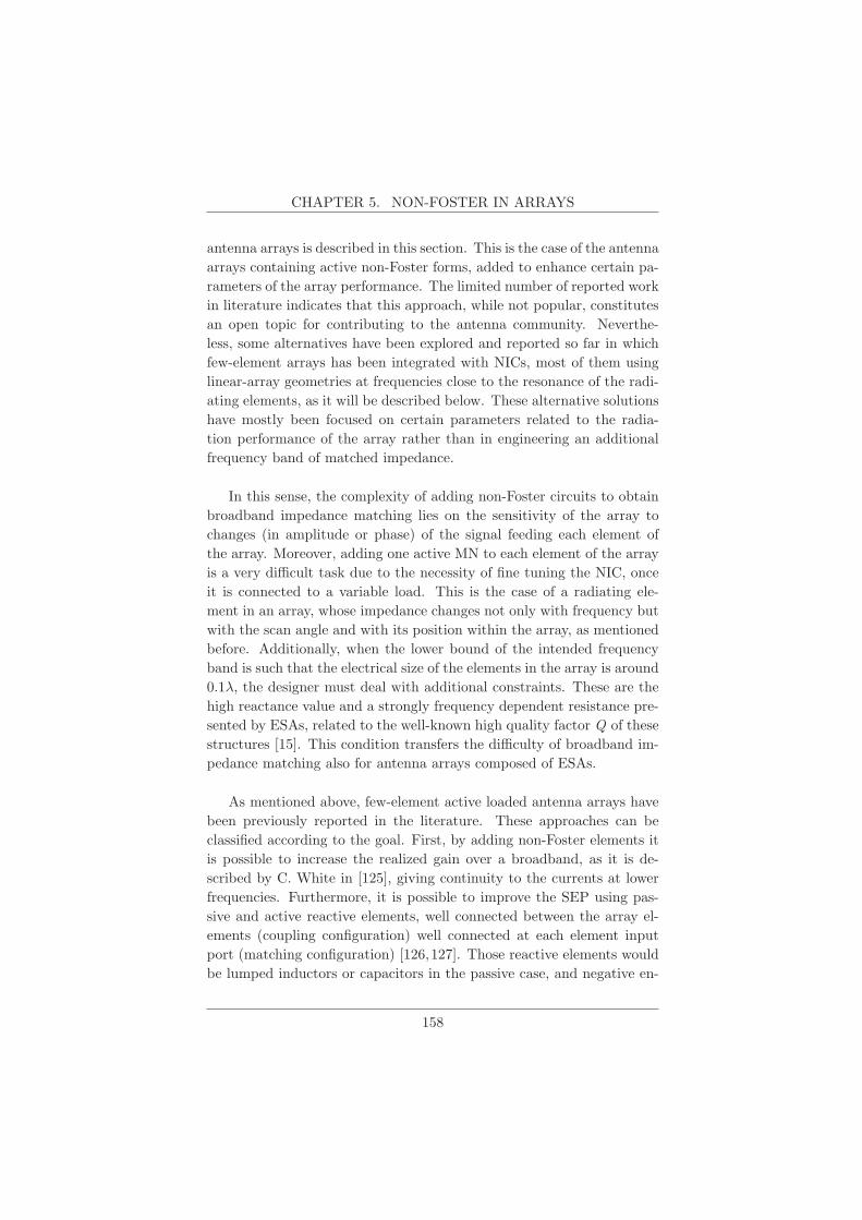
CHAPTER 5. NON-FOSTER IN ARRAYS
antenna arrays is described in this section. This is the case of the antenna
arrays containing active non-Foster forms, added to enhance certain pa-
rameters of the array performance. The limited number of reported work
in literature indicates that this approach, while not popular, constitutes
an open topic for contributing to the antenna community. Neverthe-
less, some alternatives have been explored and reported so far in which
few-element arrays has been integrated with NICs, most of them using
linear-array geometries at frequencies close to the resonance of the radi-
ating elements, as it will be described below. These alternative solutions
have mostly been focused on certain parameters related to the radia-
tion performance of the array rather than in engineering an additional
frequency band of matched impedance.
In this sense, the complexity of adding non-Foster circuits to obtain
broadband impedance matching lies on the sensitivity of the array to
changes (in amplitude or phase) of the signal feeding each element of
the array. Moreover, adding one active MN to each element of the array
is a very difficult task due to the necessity of fine tuning the NIC, once
it is connected to a variable load. This is the case of a radiating ele-
ment in an array, whose impedance changes not only with frequency but
with the scan angle and with its position within the array, as mentioned
before. Additionally, when the lower bound of the intended frequency
band is such that the electrical size of the elements in the array is around
0.1λ, the designer must deal with additional constraints. These are the
high reactance value and a strongly frequency dependent resistance pre-
sented by ESAs, related to the well-known high quality factor Q of these
structures [15]. This condition transfers the difficulty of broadband im-
pedance matching also for antenna arrays composed of ESAs.
As mentioned above, few-element active loaded antenna arrays have
been previously reported in the literature. These approaches can be
classified according to the goal. First, by adding non-Foster elements it
is possible to increase the realized gain over a broadband, as it is de-
scribed by C. White in [125], giving continuity to the currents at lower
frequencies. Furthermore, it is possible to improve the SEP using pas-
sive and active reactive elements, well connected between the array el-
ements (coupling configuration) well connected at each element input
port (matching configuration) [126,127]. Those reactive elements would
be lumped inductors or capacitors in the passive case, and negative en-
158

5.2. ANTENNA ARRAYS WITH NON-FOSTER FORMS
gineered capacitors or inductors implemented by means of NICs for the
active ones.
Second, by including Negative Group Delay (NGD) networks (to ob-
tain fast-wave propagation) in the feed network of a linear array, as pro-
posed by H. Mirzaei and G. Eleftheriades in [73]. This approach looks
for reducing the inherent beam-squinting of a linear array of tapered-
slot antennas, over a FBW of 40%, by loading the transmission lines in
the feed-network with non-Foster circuits. Additionally, a parasitic two-
element monopole array loaded with a NIC is proposed by M. Jacob et al.
in [128]. In this approach, the total array pattern takes advantage of the
property of increasing phase-response (i.e. another behavior inherent to
non-Foster circuits) of the NICs with frequency, looking for a broadband
squint-free and steerable pattern. The broadband pattern steered is re-
ported in a band (180 to 350 MHz) over which the impedance matching
is provided by the natural response of the driving element, a printed
elliptical monopole, 45 cm in length, whose resonant frequency (λ0/4)
is close to 330 MHz. Third, a more specific approach has been recently
reported by A. Elfrgani and R. Rojas in [129], in which an active non-
Foster coupling network is implemented to improve the direction-finding
capability of a Biomimetic Antenna Array (BMAA) —a two-element an-
tenna array inspired on the hearing mechanism of insects— over a wide
band. In this approach, BJT-based NIC is used as the main part of a
external coupling network, added to increase the output phase response,
relative to the incident signal angle (input phase), measured in the el-
ement terminals of the array. The elements consist of two wire-type
monopoles, 7.5 cm in length, spaced 4 cm to each other (0.13 λ0). The
reported results show an improvement in the output phase response in
the range from 420 to 550 MHz (f0 = 1 GHz).
For the sake of completeness, the alternative of embedding an active
non-Foster MN into a few-element array is explored in the subsequent
sections of this chapter. The design methodology developed throughout
this work is applied to a couple of design examples, looking for broadband
impedance matching at a new lower band. The goal is to observe the
performance of antenna arrays when loaded with an embedded active
non-Foster MN. In response to the difficulties lying on this purpose,
as described before, the design examples that will be presented here
are simple structures of few radiating elements which meet the ESA
159

CHAPTER 5. NON-FOSTER IN ARRAYS
definition (ka < 0.5).
5.3 Design Examples
The first design example presented here comprises a two-element lin-
ear array composed of two printed semiloops, arranged in a coplanar
configuration. This array is intended to be matched at the VHF band
through a NIC, once the sensitivity analysis takes place. In the second
design example, a small printed log-periodic array is involved in the same
active matching process, aided by the proposed Sens parameter, in order
to add a new working frequency interval at the lower part of the UHF
band. Some considerations are also described in terms of NIC selection,
radiation performance and stability.
5.3.1 Active Matching of a Two-Element Semiloop Ar-
ray
A linear array, composed of two coplanar semiloops as it is shown in
Fig. 5.5, connected through a non-Foster MN in a coupling configuration,
is presented as a comparative design between two cases: an ideal non-
Foster MN (a series negative inductor, L < 0) and a BJT based balanced
NIC acting as the active-MN. A FR4 slab, with εr = 4.3 and 1.5 mm
thick, contains the coplanar array elements. The design aims at matching
the array at the VHF band (under 300 MHz). The natural frequency
for the array (λ0 = 2πR) is about 1200 MHz, where the typical double
lobe (i.e. along the +z and −z axis) is observed for a λ0/2 separation
between elements.
The multi-port antenna approach, presented in Chapter 3, is used
to deduce the analytical impedance, Zan
MN, that has to be implemented
either with an ideal non-Foster MN or with a transistorized circuit (a
NIC) for broadband impedance matching. The Sens parameter plays
again an important role in the design process. As it was shown in Chap-
ter 4, the most suitable location for an active-MN in a single semiloop
was found by introducing an analytical second port. Such location is
on the opposite side from the input port. In this case, the analytical
port is a third one (see Fig. 5.5), added for full-wave simulation to ex-
tract a 3-port S-parameter matrix for each port-3 position. Due to the
160
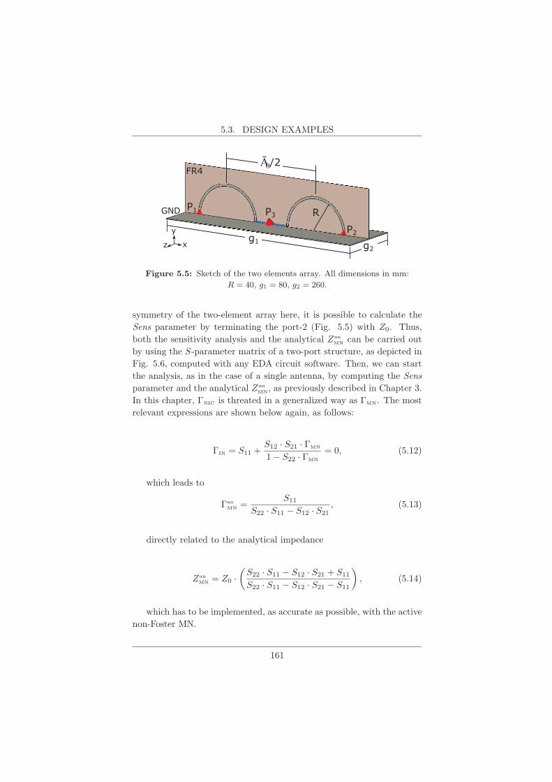
5.3. DESIGN EXAMPLES
g1 g2
RP3
x
y
z
GND
FR4
P1
P2
Ā0/2
Figure 5.5: Sketch of the two elements array. All dimensions in mm:
R = 40, g1 = 80, g2 = 260.
symmetry of the two-element array here, it is possible to calculate the
Sens parameter by terminating the port-2 (Fig. 5.5) with Z0. Thus,
both the sensitivity analysis and the analytical Zan
MN can be carried out
by using the S-parameter matrix of a two-port structure, as depicted in
Fig. 5.6, computed with any EDA circuit software. Then, we can start
the analysis, as in the case of a single antenna, by computing the Sens
parameter and the analytical Zan
MN, as previously described in Chapter 3.
In this chapter, ΓNIC is threated in a generalized way as ΓMN. The most
relevant expressions are shown below again, as follows:
ΓIN = S11 +S12 · S21 · ΓMN
1− S22 · ΓMN
= 0, (5.12)
which leads to
Γan
MN =S11
S22 · S11 − S12 · S21, (5.13)
directly related to the analytical impedance
Zan
MN = Z0 ·(S22 · S11 − S12 · S21 + S11
S22 · S11 − S12 · S21 − S11
), (5.14)
which has to be implemented, as accurate as possible, with the active
non-Foster MN.
161
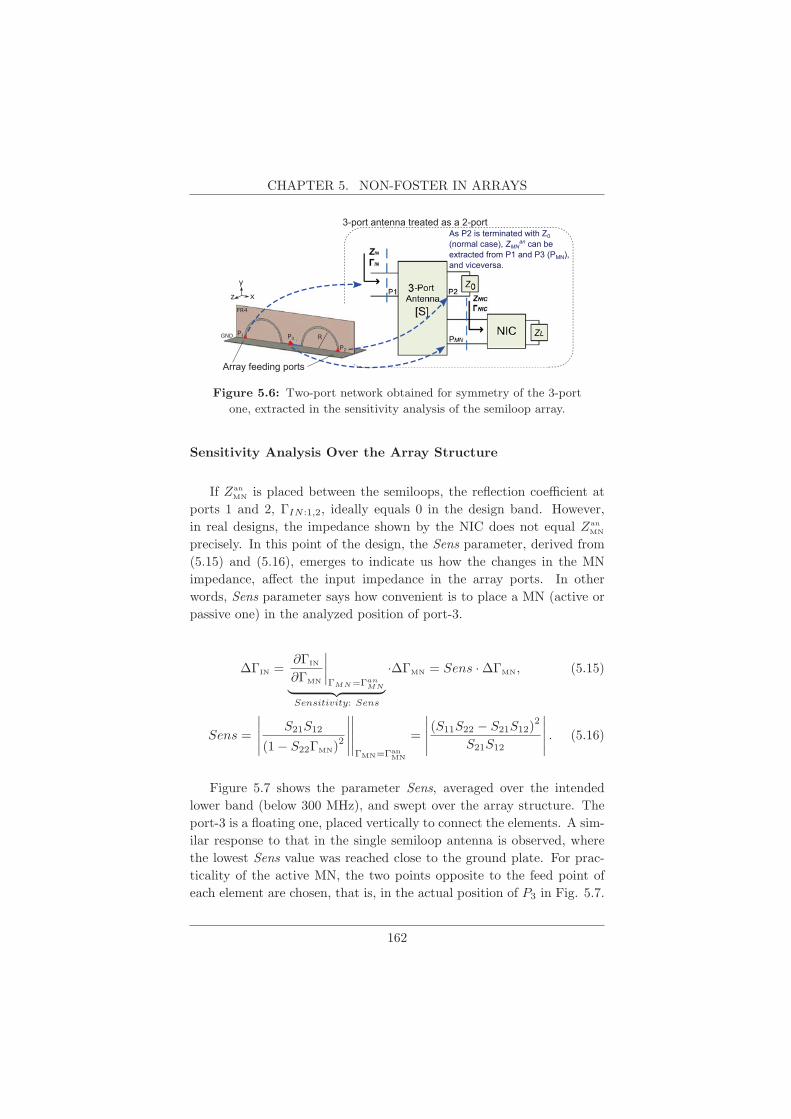
CHAPTER 5. NON-FOSTER IN ARRAYS
x
y
z
RP3GND
FR4
P1
P2
As P2 is terminated with Z0(normal case), ZMN
an can be extracted from P1 and P3 (PMN), and viceversa.
3-port antenna treated as a 2-port
Array feeding ports
Figure 5.6: Two-port network obtained for symmetry of the 3-port
one, extracted in the sensitivity analysis of the semiloop array.
Sensitivity Analysis Over the Array Structure
If Zan
MN is placed between the semiloops, the reflection coefficient at
ports 1 and 2, ΓIN :1,2, ideally equals 0 in the design band. However,
in real designs, the impedance shown by the NIC does not equal Zan
MN
precisely. In this point of the design, the Sens parameter, derived from
(5.15) and (5.16), emerges to indicate us how the changes in the MN
impedance, affect the input impedance in the array ports. In other
words, Sens parameter says how convenient is to place a MN (active or
passive one) in the analyzed position of port-3.
ΔΓIN =∂ΓIN
∂ΓMN
∣∣∣∣ΓMN=Γan
MN︸ ︷︷ ︸Sensitivity: Sens
·ΔΓMN = Sens ·ΔΓMN, (5.15)
Sens =
∣∣∣∣∣ S21S12
(1− S22ΓMN)2
∣∣∣∣∣∣∣∣∣∣ΓMN=Γan
MN
=
∣∣∣∣∣ (S11S22 − S21S12)2
S21S12
∣∣∣∣∣ . (5.16)
Figure 5.7 shows the parameter Sens, averaged over the intended
lower band (below 300 MHz), and swept over the array structure. The
port-3 is a floating one, placed vertically to connect the elements. A sim-
ilar response to that in the single semiloop antenna is observed, where
the lowest Sens value was reached close to the ground plate. For prac-
ticality of the active MN, the two points opposite to the feed point of
each element are chosen, that is, in the actual position of P3 in Fig. 5.7.
162
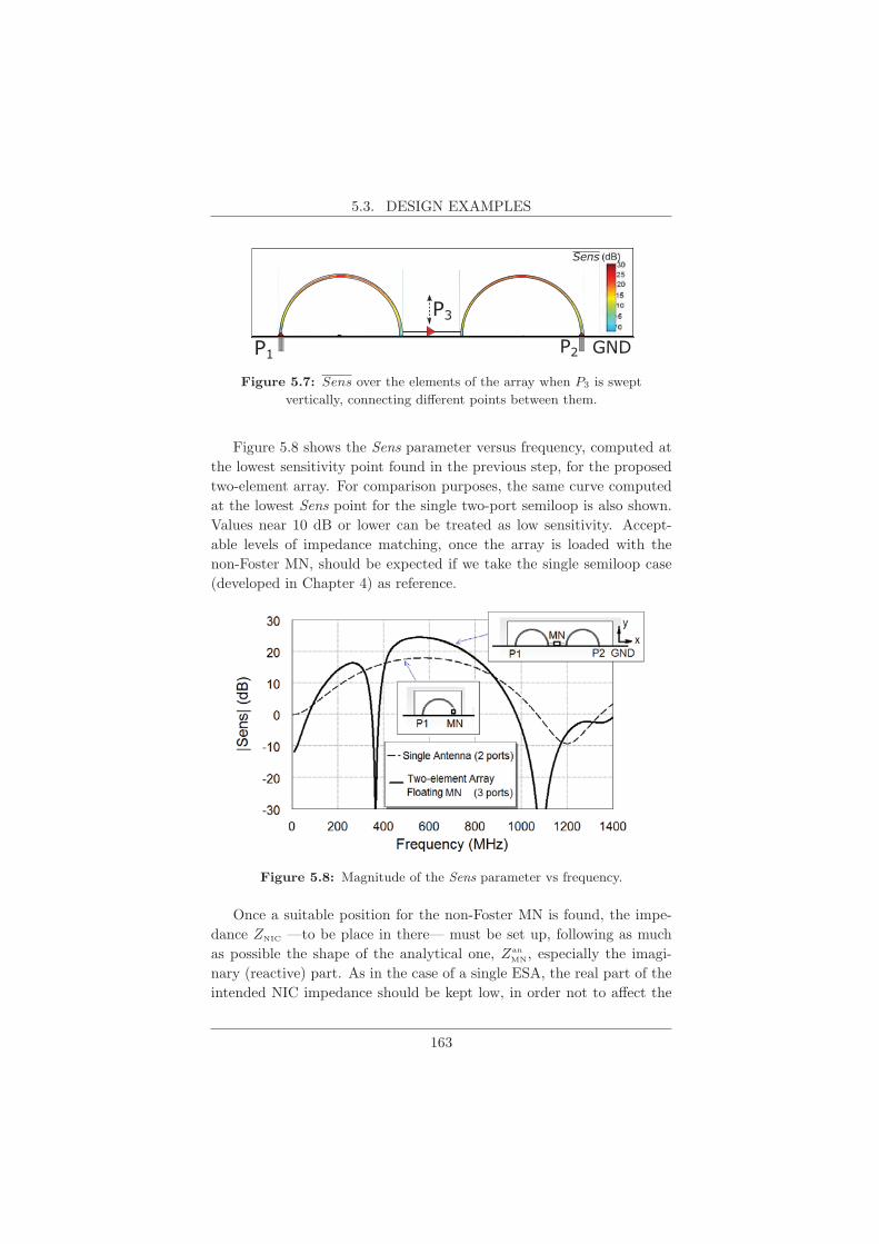
5.3. DESIGN EXAMPLES
P1 P2 GND
P3
Sens
Figure 5.7: Sens over the elements of the array when P3 is swept
vertically, connecting different points between them.
Figure 5.8 shows the Sens parameter versus frequency, computed at
the lowest sensitivity point found in the previous step, for the proposed
two-element array. For comparison purposes, the same curve computed
at the lowest Sens point for the single two-port semiloop is also shown.
Values near 10 dB or lower can be treated as low sensitivity. Accept-
able levels of impedance matching, once the array is loaded with the
non-Foster MN, should be expected if we take the single semiloop case
(developed in Chapter 4) as reference.
Figure 5.8: Magnitude of the Sens parameter vs frequency.
Once a suitable position for the non-Foster MN is found, the impe-
dance ZNIC —to be place in there— must be set up, following as much
as possible the shape of the analytical one, Zan
MN, especially the imagi-
nary (reactive) part. As in the case of a single ESA, the real part of the
intended NIC impedance should be kept low, in order not to affect the
163
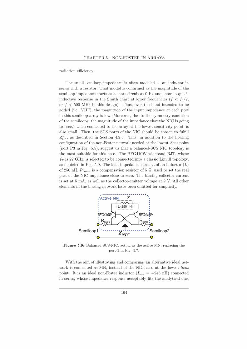
CHAPTER 5. NON-FOSTER IN ARRAYS
radiation efficiency.
The small semiloop impedance is often modeled as an inductor in
series with a resistor. That model is confirmed as the magnitude of the
semiloop impedance starts as a short-circuit at 0 Hz and shows a quasi-
inductive response in the Smith chart at lower frequencies (f < f0/2,
or f < 500 MHz in this design). Thus, over the band intended to be
added (i.e. VHF), the magnitude of the input impedance at each port
in this semiloop array is low. Moreover, due to the symmetry condition
of the semiloops, the magnitude of the impedance that the NIC is going
to “see,” when connected to the array at the lowest sensitivity point, is
also small. Then, the SCS ports of the NIC should be chosen to fulfill
Zan
MN, as described in Section 4.2.3. This, in addition to the floating
configuration of the non-Foster network needed at the lowest Sens point
(port P3 in Fig. 5.5), suggest us that a balanced-SCS NIC topology is
the most suitable for this case. The BFG410W wideband BJT, whose
fT is 22 GHz, is selected to be connected into a classic Linvill topology,
as depicted in Fig. 5.9. The load impedance consists of an inductor (L)
of 250 nH. Rcomp is a compensation resistor of 5 Ω, used to set the real
part of the NIC impedance close to zero. The biasing collector current
is set at 5 mA, as well as the collector-emitter voltage at 2 V. All other
elements in the biasing network have been omitted for simplicity.
Semiloop1 Semiloop2
ZL
ZNIC
BFG410WBFG410W
Active MN
Rcomp
L=250 nH
Rcomp
Figure 5.9: Balanced SCS-NIC, acting as the active MN; replacing the
port-3 in Fig. 5.7.
With the aim of illustrating and comparing, an alternative ideal net-
work is connected as MN, instead of the NIC, also at the lowest Sens
point. It is an ideal non-Foster inductor (Lneg = −248 nH) connected
in series, whose impedance response acceptably fits the analytical one.
164

5.3. DESIGN EXAMPLES
This fact confirms the simplicity of the needed non-Foster network for
this design, even though it is an idealized case. Figure 5.10 shows the
behavior of Zan
MN versus frequency, as well as the ideal series negative
inductor and the BJT-based NIC.
Figure 5.10: Impedance response of ZanMN, the ideal negative inductor,
and the balanced BJT-based NIC.
For frequencies above 300 MHz, the array shall be difficult to match
because of the resonant-like response of Zan
MN. A reduced span in the
previous figure let us to observe how much the NIC impedance fits the
analytical one, as shown in Fig. 5.11. In the proposed design strat-
egy, a visual inspection aided by the EDA software reduces greatly the
complexity of fitting the actual NIC impedance to the analytical Zan
MN.
It is worth noting that the maximum frequency at which the NIC
acts as an active MN is expected to be around 300 MHz. Above this
frequency, the reactance of Zan
MN changes abruptly, being impossible to
follow with a single NIC. That frequency corresponds to the upper bound
of the lower band obtained (S11 < −10dB), as the S11 parameter, com-
puted when the other element of the array is Z0 terminated, shows in
Fig. 5.12.
165

CHAPTER 5. NON-FOSTER IN ARRAYS
10 60 110 160 210 260 300Frequency (MHz)
-400
-300
-200
-100
050
Impe
danc
e (Ā
)Ideal MN. Real part.Ideal MN. Imag. part.
ZMNan. Real part.
ZMNan. Imag. part.
Balanced NIC. Real part
Balanced NIC. Imag. part
Figure 5.11: Reduced span for the impedance response of ZanMN, the
ideal negative inductor, and the balanced BJT-based NIC.
Stability Analysis
Following the design method presented in Chapter 4, the stability of
the complete actively matched array (array + NIC) is checked. The NDF
is computed in the AWR design software, by using the linear small-signal
model of the transistors at the selected biasing point, including package
effects and the transmission lines. The S-parameters matrix of the 3-
port array, extracted in the sensitivity analysis step, is also included in
the NDF calculation. The NDF is calculated along the interval from
-300 GHz to 300 GHz, as shown in Fig. 5.13. A zoom-in around the
origin is also shown. Since the fT parameter of the used BJT is 22 GHz,
computing the NDF up to 300 GHz is a reasonable decision to look for
oscillations or any other instability phenomenon. It can be observed
that there are no origin encirclements. This fact predicts stability in the
overall design, as mentioned earlier.
Radiation performance
In terms of radiation performance, an omnidirectional response in the
plane containing the elements, in the lower VHF band (at 100 MHz), is
found for both the NIC-loaded array, and the unloaded array, as can be
seen in the upper row of Fig. 5.14. This pattern is the one expected
from a small loop antenna, which is often referred as the “magnetic
166
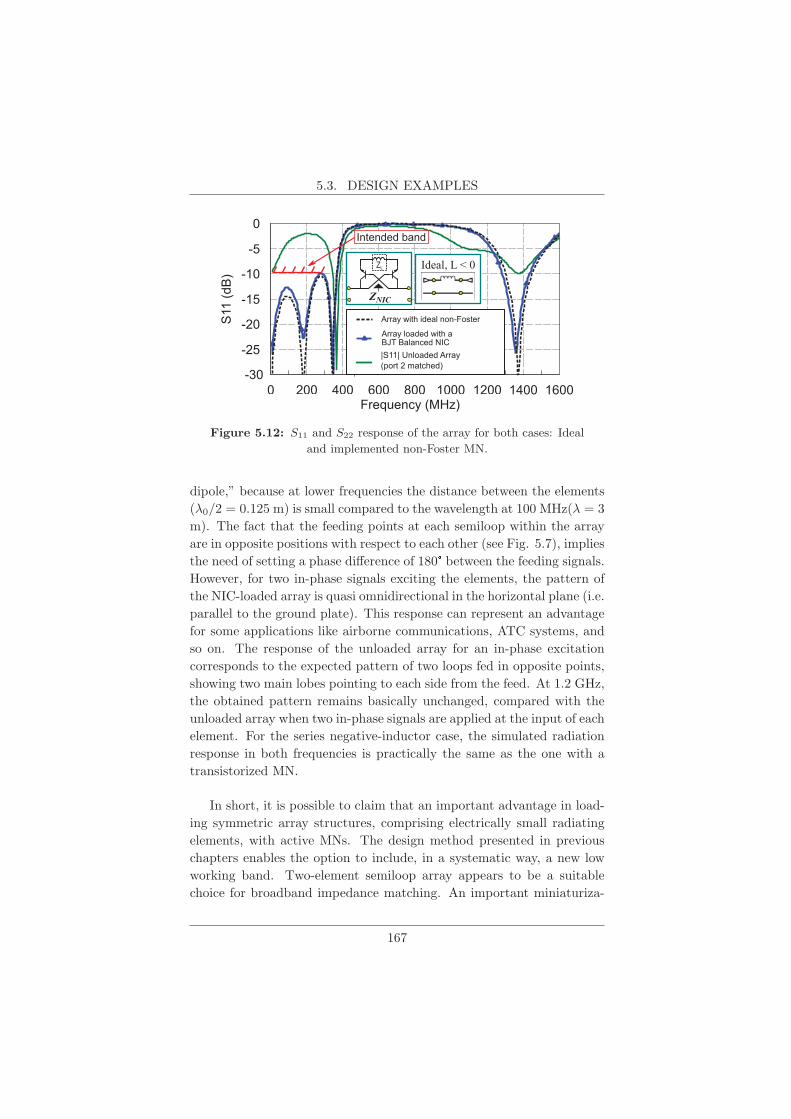
5.3. DESIGN EXAMPLES
0 200 400 600 800 1000 1200 1400 1600Frequency (MHz)
-30
-25
-20
-15
-10
-5
0S
11 (d
B)
Array with ideal non-Foster
Array loaded with aBJT Balanced NIC|S11| Unloaded Array(port 2 matched)
Ideal, L < 0ZL
ZNIC
Intended band
Figure 5.12: S11 and S22 response of the array for both cases: Ideal
and implemented non-Foster MN.
dipole,” because at lower frequencies the distance between the elements
(λ0/2 = 0.125 m) is small compared to the wavelength at 100 MHz(λ = 3
m). The fact that the feeding points at each semiloop within the array
are in opposite positions with respect to each other (see Fig. 5.7), implies
the need of setting a phase difference of 180� between the feeding signals.
However, for two in-phase signals exciting the elements, the pattern of
the NIC-loaded array is quasi omnidirectional in the horizontal plane (i.e.
parallel to the ground plate). This response can represent an advantage
for some applications like airborne communications, ATC systems, and
so on. The response of the unloaded array for an in-phase excitation
corresponds to the expected pattern of two loops fed in opposite points,
showing two main lobes pointing to each side from the feed. At 1.2 GHz,
the obtained pattern remains basically unchanged, compared with the
unloaded array when two in-phase signals are applied at the input of each
element. For the series negative-inductor case, the simulated radiation
response in both frequencies is practically the same as the one with a
transistorized MN.
In short, it is possible to claim that an important advantage in load-
ing symmetric array structures, comprising electrically small radiating
elements, with active MNs. The design method presented in previous
chapters enables the option to include, in a systematic way, a new low
working band. Two-element semiloop array appears to be a suitable
choice for broadband impedance matching. An important miniaturiza-
167

CHAPTER 5. NON-FOSTER IN ARRAYS
Figure 5.13: NDF plotted up to 300 GHz to check the stability of the
actively matched semiloop array.
tion level can be obtained in a low-cost and easy-to-manufacture array.
Even though there are changes in the radiation pattern in the engineered
lower band, the antenna system can still be attractive for some applica-
tions.
5.3.2 Small Printed Log-Periodic Array, Matched with
an Active non-Foster Network
In order to show a different design example, the design of a small
printed-log-periodic antenna loaded with an active MN for multi-band
applications is presented in this section. A well-known, low-cost, and
low-profile antenna is re-engineered for including an additional broad
impedance band in the upper VHF- and the lower UHF-band (from 30
to 720 MHz), maintaining its natural broadband response (around 2.3
GHz). The design method involves again the methodology described in
Chapter 4, by means of the sensitivity parameter Sens, to find a suitable
location for a transistor-based non-Foster network (a NIC). A BJT-based
balanced NIC is selected to act as active MN, after an impedance analysis
that will be shown below.
A log-periodic array of printed dipoles consists of a group of dipoles
which follows a logarithmic relation with frequency [24]. This configu-
ration is well-known for broadband applications in frequencies at which
the length of the array elements is around half-wavelength (λ/2), that is,
168

5.3. DESIGN EXAMPLES
Figure 5.14: 3D plot of the radiation response for a two-element
semiloop array, at different frequencies for both the unloaded and
NIC-loaded cases.
from 1.8 to 2.7 GHz for this case (FBW = 40%). However, at lower fre-
quencies, important constraints arise in terms of gain-bandwidth when
the intended operating band is designed to include a passive network,
as the Bode-Fano criteria states [11]. An additional design constraint
arises from the high-Q condition of ESAs, described before.
The antenna under study is composed of two dipoles (see Fig. 5.15).
These dipoles are implemented by using an antipodal configuration (each
branch of the dipole is printed on one side of a dielectric substrate). Each
element is fed through a parallel plate line, so the array has just one
physical feeding port (P1 in Fig. 5.15), and can be treated as a single
antenna for the active matching procedure. In this case, a slab of FR4
169
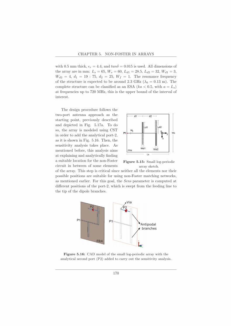
CHAPTER 5. NON-FOSTER IN ARRAYS
with 0.5 mm thick, εr = 4.4, and tanδ = 0.015 is used. All dimensions of
the array are in mm: Ls = 65, Ws = 60, Ld1 = 28.5, Ld2 = 32, Wd1 = 3,
Wd2 = 4, d1 = 19 : 75, d2 = 25, Wf = 1. The resonance frequency
of the structure is expected to be around 2.3 GHz (λ0 = 0.13 m). The
complete structure can be classified as an ESA (ka < 0.5, with a = Ls)
at frequencies up to 720 MHz, this is the upper bound of the interval of
interest.
Figure 5.15: Small log-periodic
array sketch.
The design procedure follows the
two-port antenna approach as the
starting point, previously described
and depicted in Fig. 5.17a. To do
so, the array is modeled using CST
in order to add the analytical port-2,
as it is shown in Fig. 5.16. Then, the
sensitivity analysis takes place. As
mentioned before, this analysis aims
at explaining and analytically finding
a suitable location for the non-Foster
circuit in between of some elements
of the array. This step is critical since neither all the elements nor their
possible positions are suitable for using non-Foster matching networks,
as mentioned earlier. For this goal, the Sens parameter is computed at
different positions of the port-2, which is swept from the feeding line to
the tip of the dipole branches.
Antipodal branches
Via
FR4
Figure 5.16: CAD model of the small log-periodic array with the
analytical second port (P2) added to carry out the sensitivity analysis.
170
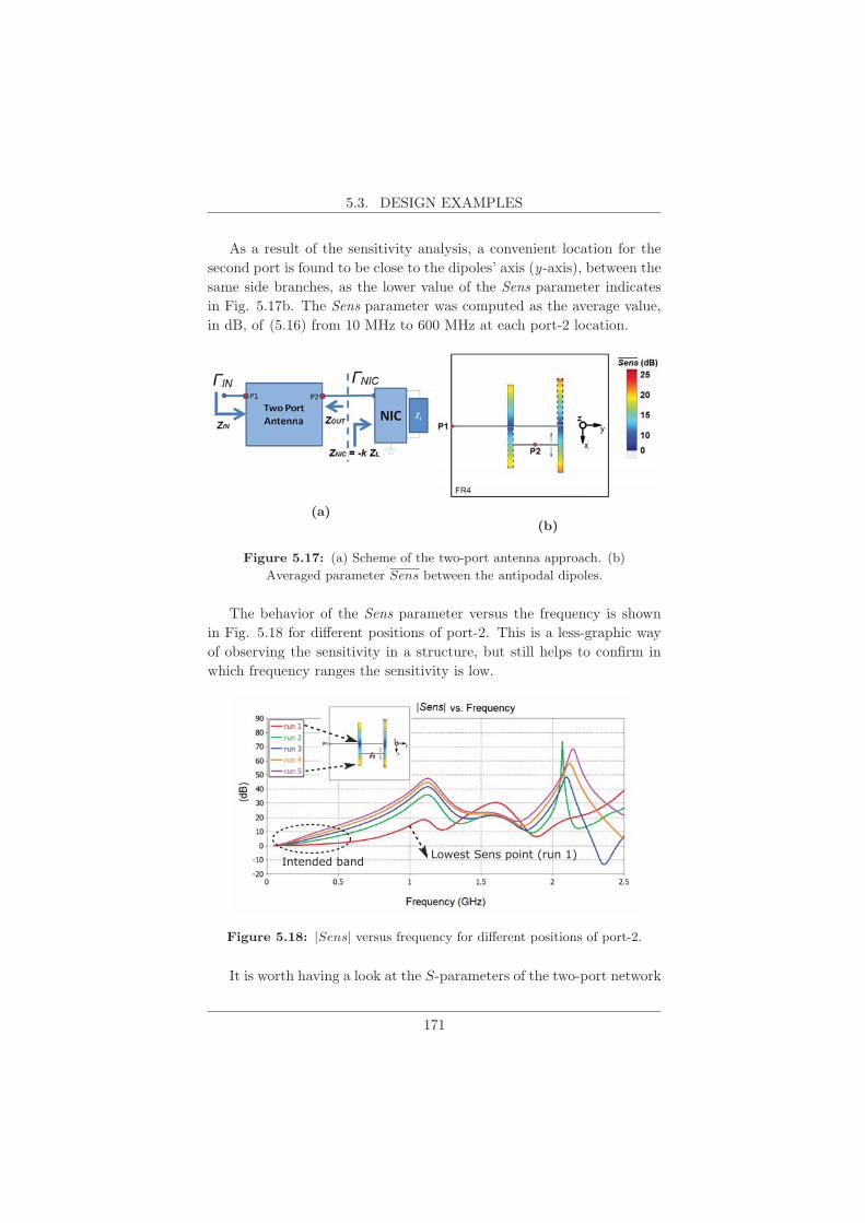
5.3. DESIGN EXAMPLES
As a result of the sensitivity analysis, a convenient location for the
second port is found to be close to the dipoles’ axis (y-axis), between the
same side branches, as the lower value of the Sens parameter indicates
in Fig. 5.17b. The Sens parameter was computed as the average value,
in dB, of (5.16) from 10 MHz to 600 MHz at each port-2 location.
(a)(b)
Figure 5.17: (a) Scheme of the two-port antenna approach. (b)
Averaged parameter Sens between the antipodal dipoles.
The behavior of the Sens parameter versus the frequency is shown
in Fig. 5.18 for different positions of port-2. This is a less-graphic way
of observing the sensitivity in a structure, but still helps to confirm in
which frequency ranges the sensitivity is low.
Lowest Sens point (run 1)Intended band
Figure 5.18: |Sens| versus frequency for different positions of port-2.
It is worth having a look at the S-parameters of the two-port network
171
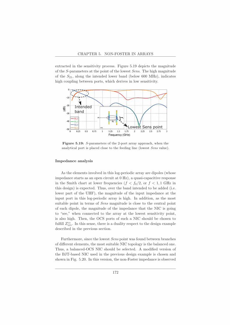
CHAPTER 5. NON-FOSTER IN ARRAYS
extracted in the sensitivity process. Figure 5.19 depicts the magnitude
of the S-parameters at the point of the lowest Sens. The high magnitude
of the S21, along the intended lower band (below 600 MHz), indicates
high coupling between ports, which derives in low sensitivity.
Lowest Sens point
Intendedband
Lowest Sens point
Intendedband
Figure 5.19: S-parameters of the 2-port array approach, when the
analytical port is placed close to the feeding line (lowest Sens value).
Impedance analysis
As the elements involved in this log-periodic array are dipoles (whose
impedance starts as an open circuit at 0 Hz), a quasi-capacitive response
in the Smith chart at lower frequencies (f < f0/2, or f < 1, 1 GHz in
this design) is expected. Thus, over the band intended to be added (i.e.
lower part of the UHF), the magnitude of the input impedance at the
input port in this log-periodic array is high. In addition, as the most
suitable point in terms of Sens magnitude is close to the central point
of each dipole, the magnitude of the impedance that the NIC is going
to “see,” when connected to the array at the lowest sensitivity point,
is also high. Then, the OCS ports of such a NIC should be chosen to
fulfill Zan
MN. In this sense, there is a duality respect to the design example
described in the previous section.
Furthermore, since the lowest Sens point was found between branches
of different elements, the most suitable NIC topology is the balanced one.
Thus, a balanced-OCS NIC should be selected. A modified version of
the BJT-based NIC used in the previous design example is chosen and
shown in Fig. 5.20. In this version, the non-Foster impedance is observed
172

5.3. DESIGN EXAMPLES
looking inside from the emitter of each BJT. The Rcomp, whose value is
9.6 Ω, is now located in series with the load inductor (L = 17 nH).
Semiloop1 Semiloop2ZNIC
BFG410WBFG410W
Active MN
L=17nH
Rcomp
Rcomp
Figure 5.20: Balanced BJT-based OCS NIC topology used to actively
match the log-periodic array.
The NIC impedance of the BJT-based network is analyzed to fit the
analytical impedance derived from the S-parameters in the lowest Sens
point (2 mm above the feeding line in Fig. 5.17b). The AWR software
is used to carry out the impedance analysis.
Figure 5.21 shows the impedance behavior of the NICs, in simulation,
compared to the analytical Zan
MN. The impedance implemented with the
BJT-based NIC, ZNIC-BJT, offers the possibility of compensating the re-
sistive part, letting us to control the tradeoff between impedance band-
width and radiation efficiency of the loaded array. The reactive response
of the NIC impedance agrees successfully with the analytical one.
Figure 5.21: Computed ZanMN versus the simulated NIC impedance for
the BJT-based NIC.
173

CHAPTER 5. NON-FOSTER IN ARRAYS
The simulated S11 parameter for the NIC-loaded case is depicted in
Fig. 5.22. Once loaded, the log-periodic array still presents an impe-
dance FBW of over 40% (S11 < −10 dB) in its natural band (centered at
2.25 GHz). In the new VHF-UHF engineered band, the targeted match-
ing level (S11 < −8 dB) is obtained over the entire range of interest.
In fact, the resulting lower band is from 0 MHz to 900 MHz. It is an
encouraging result, at least in simulation, for such an electrically small
printed structure. One advantageous property of this NIC topology is
the capability of adjusting the matching level within the added band.
This is made by changing the Rcomp value, as mentioned before, in case
of experimenting a substantial reduction in the overall gain.
0 300 600 900 1200 1500 1800 2100 2400 2700 3000
Frequency (MHz)
-20
-15
-10
-5
0
S11
(dB
)
Unloaded Array
BJT-NIC loaded
Intended band
ESA limit (720 MHz)
Figure 5.22: S11 parameter of the log-periodic array when loaded with
a balanced-OCS BJT-based NIC.
Radiation considerations
The radiation response is studied for the NIC loading the small log-
periodic array in comparison with the unloaded case. At the engineered
lower band, it can be observed the quasi-omnidirectional pattern in the
xz -plane (i.e. orthogonal to both the substrate and the dipoles) for the
NIC-loaded antenna, depicted in Fig. 5.23. Similar directivity values
compared to the unloaded case are obtained, but without the character-
istic nulls on the “doughnut-like” pattern of a small dipole. This fact
indicates a slight modification in the current distribution across the ar-
ray by introducing an active MN. Nonetheless, the obtained radiation
pattern is still attractive for some applications, as it was claimed in the
small semiloop array example.
174
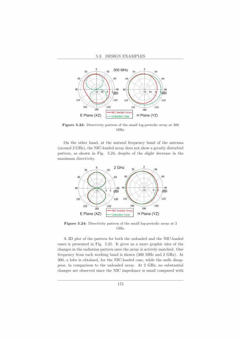
5.3. DESIGN EXAMPLES
Figure 5.23: Directivity pattern of the small log-periodic array at 300
MHz.
On the other hand, at the natural frequency band of the antenna
(around 2 GHz), the NIC-loaded array does not show a greatly disturbed
pattern, as shown in Fig. 5.24, despite of the slight decrease in the
maximum directivity.
2 GHz
dBi dBi
E Plane (XZ) H Plane (YZ)
Figure 5.24: Directivity pattern of the small log-periodic array at 2
GHz.
A 3D plot of the pattern for both the unloaded and the NIC-loaded
cases is presented in Fig. 5.25. It gives us a more graphic idea of the
changes in the radiation pattern once the array is actively matched. One
frequency from each working band is shown (300 MHz and 2 GHz). At
300, a lobe is obtained, for the NIC-loaded case, while the nulls disap-
pear, in comparison to the unloaded array. At 2 GHz, no substantial
changes are observed since the NIC impedance is small compared with
175

CHAPTER 5. NON-FOSTER IN ARRAYS
the array impedance.
Figure 5.25: 3D plot of the simulated directivity pattern of the small
log-periodic array.
5.4 Conclusion
The embedded active matching network (MN) is an interesting option
to manage an additional working band at frequencies where the array is
electrically small. The design strategy presented in Chapter 4 appears
to be an interesting way to face the impedance matching limitations of
such electrically small structures. Similarly, this method let us to make
use of the available computational power through the use of electromag-
netic full-wave and the EDA circuit simulators. The Sens parameters
provide the designer with additional considerations related to the most
suitable location to add an active non-Foster MN. The easy-to-compute
impedance Zan
MN enables a fitting process of the active MN performance
at any EDA software, besides the possibility of comparing several NIC
topologies for the same radiating structure.
Nevertheless, due to the non-zero resistive part of the NIC, the radi-
ation efficiency at the lower band is expected to be low. Thus, further
176

5.4. CONCLUSION
efforts have to be made to compensate its effect and mitigate this draw-
back, based on the tradeoff between radiation efficiency and matching
level. Then, an active non-Foster MN in which the resistive part can
be controlled or compensated is advantageous for the active impedance
matching approach for arrays containing ESAs.
177


CHAPTER 6
CONCLUSIONS AND FUTURE WORK
6.1 Summary and Conclusion
The main goal of this thesis has been the development of multiband
antennas with an engineered lower broadband obtained by embedding
an active non-Foster matching network (MN).
It is not easy to summarize in a few paragraphs all the work un-
dertaken and the observations collected in these last years of realization
of this doctoral thesis. However, in the following lines, the most rele-
vant conclusions are presented. The major difficulties observed through-
out this work, that arise when the antenna engineer attempts to design
actively-matched electrically small antennas (ESAs) loaded with non-
Foster matching networks (MNs) are also described.
In Chapter 2 the background and the most relevant work related
to ESAs, its classification, its performance limitations, and the evolu-
tion of the techniques to overcome such limitations were presented. The
high-quality factor Q of the ESAs —and the gain-bandwidth limita-
tions inherent to it— represents one of the most challenging tasks to
be addressed when any type of impedance MN is to be included in the
antenna system. Among the alternatives to enhance the ESAs perfor-
mance, the non-Foster showed up as an interesting and effective way
CHAPTER 6. SUMMARY
to obtain broad-instantaneous impedance bandwidth. Those techniques
and results became the cornerstone of the work developed and presented
afterward in this document.
A novel parameter, called Sens, was introduced in Chapter 3 as an
easy-to-calculate and versatile S-parameter based tool which is useful
to analyze the feasibility of the embedding non-Foster MNs approach
for the actual antenna. Thus, Sens parameter let us know whether the
antenna under study is suitable to be loaded with an active non-Foster
MN and, if so, it tells us what is the best location to place the MN.
The breakthrough with the Sens parameter is its property of easily be
computed in any full-wave CAD software, as well as, that it can be used
with any other type of antenna disregarding its electrical size.
Chapter 4 presented another contribution of this dissertation: the
design method for designing electrically small antennas actively matched
with embedded non-Foster forms. It can be said that any compendium
of considerations, presented as a to-do list of steps, gives to the engineer
an additional discernment and decision tool. This design strategy aims
at contributing with additional considerations, organized in an integral
methodology, to reduce as much as possible the percentage of failure
when a design is taken from the simulation and the calculations stage to
the practice.
The strategy of embedding the active matching network is presented
as an interesting alternative, especially for those applications where the
space occupied by the antenna and all its circuitry is limited and com-
prises a determining factor in their design. In this sense, two different
structures: a printed small semiloop antenna and a printed small blade-
type monopole were presented as design examples applying the proposed
method. An important miniaturization level was reached in both anten-
nas at the lower bound of the engineered lower band (up to 90% and 95%
in the semiloop and the blade-monopole respectively), compared to the
full-size resonant antenna of each type. Besides the miniaturization level,
the impedance FBW obtained at the added band were 119%, centered
at 117 MHz, for the semiloop (ka factor from 0.04 to 0.17), and over
82%, centered at 85 MHz, for the blade-monopole (ka factor from 0.26
to 0.56). It is worth mentioning that the natural impedance response of
each antenna was not affected once the active-MN was embedded. The
180
6.1. SUMMARY AND CONCLUSION
notable impedance bandwidth performance reached in both structures
encouraged us to keep seeking solutions to the changes in the radiation
pattern, which resulted after adding the active non-Foster MN into the
antennas.
Regarding the selection of the active element involved in the active
non-Foster network, it is important to point out the need to use a tran-
sistor with a constant transconductance (gm) response up to the highest
possible frequency. In addition, its transition frequency (fT ) should also
be high, since the non-Foster behavior of the associated NIC impedance
is expected to be a fraction of this value. Short feedback path-lengths
are preferred to reduce the associated inductive effect, that can lead to
oscillations in the manufactured non-Foster network. In this line, the
proposed design methodology make use of the tolerance analysis, avail-
able in many commercial circuit simulators, which give us an additional
view on those specific parameters to which the system overall perfor-
mance (antenna + NIC) is more sensitive.
The stability of the antenna system is also addressed in Chapter 4.
The NDF is used as a very interesting alternative as well as easy to cal-
culate and rigorous for the evaluation of the stability of linear systems.
Again, by using any commercial circuit design software, the stability
analysis can be generalized to include the simulated or measured S-
parameters of the antenna into the NDF computation. The parasitic or
packaging effects of the components, as well as edge effects on the micro-
strip or strip-line that connect the components, can also be considered
when computing the NDF. This fact makes the NDF be one of the most
versatile stability analysis method reported to date.
It is important to note that this methodology may be used directly in
any type of antenna, besides in a single ESA. It can be used in antennas
of any electrical size, even in presence of other radiating elements in
the near field. In this sense, Chapter 5 presented the proposed design
methodology applied to antenna arrays, in order to add an additional
lower working band. A couple of few-element arrays were presented as
design examples to illustrate the approach.
One of the facts that perhaps most discourages antennas engineers
from including active elements in their designs is the high level of effort
181

CHAPTER 6. SUMMARY
and laboratory work involved in the fine tuning of the devices, in this case
the NICs. In the clear majority of cases, as actually occurred with the
design examples shown throughout this thesis, it spends hours adjusting
and testing before achieving a successful result that fits the expected
performance.
Perhaps this last fact is one of the reasons why, for many research
groups around the world, the use of negative impedance converters,
NICs, as antenna impedance MNs, has reached the final phase of its
life-time in the research and development field. Proof of this is the small
number of teams that report contributions today. Nonetheless, it should
be noted that much work remains to be done in the realization of ESAs,
actively-matched with non-Foster networks, for them to be attractive to
the industry and the academy.
6.2 Future Lines
Arising from the research carried out during this work, areas of po-
tential further research could include the topics mentioned below.
First, parasitic effects and other inaccuracies associated with the fab-
rication of NICs on a Printed Circuit Board (PCB) board can be over-
come by means of the monolithic technology (MMICs). Although some
works have been reported as successful, it has not been possible to ex-
plore that approach in this work. Nonetheless, this is an interesting
alternative for implementing more reliable non-Foster devices to be in-
tegrated into an ESA.
Second, the use of other active devices to realize non-Foster cir-
cuits, such as the resonant tunneling diodes (RTD) operating in a Neg-
ative Differential Resistance (NDR) region, has been recently reported
in [60, 130, 131]. This approach represents an encouraging alternative
to mitigate the limited frequency problem, and the associated tradeoff
between this limitation and potential instability issues in non-Foster cir-
cuits, as reported so far. This is perhaps one of the most interesting
future lines of work that the author wants to point out.
On the other hand, the noise performance of the receiving antennas,
represented by the noise figure (NF), is a fundamental figure of merit
182
6.2. FUTURE LINES
especially when active devices are integrated into the receiver chain. Es-
timating the added noise in an actively matched ESA is not an easy task,
even less when the active-MN is embedded into the radiating structure.
Then, a quantification technique for added noise estimation is welcome
and stands for a line of future work. An interesting approach in this area
has been recently reported by M. Jacob and D. Sievenpiper in [117]. In
their work, the noise model of a BJT-based NIC, around its biasing point,
is used to estimate the added noise when connected to the feeding port
of an ESA. A comparative analysis is done for the case of a single-stage
amplifier connected directly to the feeding point (instead of the NIC) of
the same antenna.
Estimation and measurement of the actively loaded antenna perfor-
mance in transmitting mode, comprise another important topic to be
addressed in actively matched antennas area. To the best of our knowl-
edge, by embedding the non-Foster elements into the antenna, the an-
tenna system (ESA + NIC) can be used either in transmitting or receiv-
ing mode. Nonetheless, the non-linear phenomena effects, related to the
power compression and saturation of the active devices (e.g. transistors),
in presence of high voltages and currents driving the antenna, are still
a significant constraint, especially at practical transmitting power levels
(i.e. greater than 100 mW).
Finally, the manufacture of a few-element array loaded with a non-
Foster MN is a task ahead in the seeking for extending the reported
enhanced performance down in frequency. Thus, obtaining an actively
matched electrically small array with additional enhanced parameters
would be possible. Among these additional parameters it can be men-
tioned a high scan element pattern (SEP) level —a challenging task since
the coupling effects between elements increase at lower frequencies— or
an enhanced direction finding sensitivity, as it was recently proposed by
A. Elfrgani et al. in [129].
183

CONCLUSIONES Y TRABAJO FUTURO
Resumen y Conclusiones
El objetivo principal de esta tesis ha sido el desarrollo de antenas
multibanda que presenten una banda adicional de trabajo a bajas fre-
cuencias, obtenida mediante la incorporacion de una red de adaptacion
de impedancia —MN, deMatching Network— activa, de tipo non-Foster.
No es facil resumir en unos pocos parrafos todo el trabajo realizado
y las observaciones recogidas en estos ultimos anos de realizacion de esta
tesis doctoral. Sin embargo, en las lıneas siguientes, se presentan las
conclusiones mas relevantes. De igual modo, se describen las mayores
dificultades experimentadas a lo largo de este trabajo, que surgen cuando
se intenta disenar antenas electricamente pequenas (ESAs) adaptadas
con redes activas tipo non-Foster.
En el Capıtulo 2 se presentan los antecedentes y el trabajo previo mas
relevante relacionado con las ESAs, su clasificacion, sus limitaciones de
funcionamiento y la evolucion de las tecnicas para superar tales limita-
ciones. El alto factor de calidad (Q) que presentan las ESAs, sumado

CHAPTER 6. CONCLUSIONES
las limitaciones de ancho de banda y de ganancia asociados a esta carac-
terıstica, representan una de las tareas mas difıciles de tratar al incluir
cualquier tipo de red de adaptacion de impedancia en el sub-sistema ra-
diante (antena). Entre las alternativas para mejorar el desempeno de
las ESAs, los circuitos tipo non-Foster surgen como una alternativa in-
teresante y efectiva de obtener un ancho de banda —de impedancia—
instantaneo amplio. Esas tecnicas y resultados se convirtieron en la
piedra angular del trabajo desarrollado, y posteriormente presentado,
en este documento.
Un nuevo parametro, denominado Sens por el autor, fue introducido
y desarrollado en el Capıtulo 3 como una herramienta versatil y facil de
calcular, basada en los parametros S del modelo de dos puertos de la an-
tena misma, que es util para analizar la viabilidad de la integracion de
una MN tipo non-Foster en la estructura de la antena. Por lo tanto,
el parametro Sens nos permite saber si la antena estudiada es ade-
cuada para ser integrada a una MN activa, tipo non-Foster y, de ser
ası, nos indica tambien cual es la mejor ubicacion para colocar tal MN.
El avance que representa el parametro Sens radica en su propiedad de
ser facilmente calculado por medio de cualquier software de simulacion
electromagnetica, siempre que este tenga la opcion de diseno asistido por
computadora (CAD). Una propiedad adicional y no menos importante
del parametro Sens es que puede ser utilizado con cualquier otro tipo
de antena sin tener en cuenta su tamano electrico o su estructura.
En el Capıtulo 4 fue presentada otra de las contribuciones de esta
tesis: el metodo para el diseno de antenas electricamente pequenas, adap-
tadas con formas activas incorporadas tipo non-Foster. Se puede decir
que cualquier compendio de consideraciones practicas da al ingeniero
una herramienta adicional de discernimiento y decision. Esta estrategia
de diseno pretende contribuir con consideraciones adicionales, organi-
zadas en una metodologıa integral, para reducir, tanto como sea posible,
el porcentaje de fallas al abordar el diseno, desde la etapa de calculo y
simulacion, hasta la practica.
La estrategia de incorporar —embeber— la red de adaptacion ac-
tiva de impedancias, se presenta como una alternativa interesante, es-
pecialmente para aquellas aplicaciones en las que el espacio ocupado
por la antena, y todos sus circuitos, es limitado y constituye un fac-
186
tor determinante en su diseno. En este sentido, fueron presentadas dos
estructuras distintas: una antena impresa, electricamente pequena, de
tipo lazo (semiloop), y un monopolo impreso tipo aleta (blade), tambien
electricamente pequeno, como ejemplos de diseno aplicando el metodo
propuesto. Un importante nivel de miniaturizacion en ambas antenas fue
obtenido en la banda baja incorporada, de entre 90% y 95% a la frecuen-
cia mas baja, en el semiloop y el monopolo de aleta, respectivamente.
Este nivel de miniaturizacion fue calculado, en cada caso, con respecto
a una antena resonante, de igual naturaleza (magnetica o electrica), es
decir, de tamano electrico completo a dicha frecuencia.
Ademas del grado de miniaturizacion conseguido, el ancho de banda
relativo (FBW) medido, en la banda baja anadida, fue del 119% (cen-
trado en 117 MHz) para el semiloop (factor ka entre 0,04 y 0,17), y de
mas del 82% (centrado en 85 MHz) para el monopolo de aleta (factor ka
entre 0,26 y 0,56). Cabe senalar que la respuesta natural de impedancia
de cada antena no fue afectada una vez que la red de adaptacion activa
es incorporada. El notable ancho de banda de impedancia, alcanzado en
ambas estructuras, nos alento a continuar en la busqueda de soluciones
a los cambios en el diagrama de radiacion, experimentados despues de
anadir la red activa non-Foster en la estructura de la antena.
Con respecto a la seleccion del dispositivo activo a ser utilizado en
la red activa non-Foster, es importante senalar la necesidad de utilizar
un transistor con una respuesta de transconductancia (gm) constante,
hasta la maxima frecuencia posible. Ademas, su frecuencia de transicion
(fT) tambien debe ser alta, ya que se espera que el comportamiento non-
Foster de la impedancia de entrada del NIC sea una pequena fraccion de
dicha frecuencia fT. En este sentido, la metodologıa de diseno propuesta
utiliza el analisis de tolerancia, disponible en muchos simuladores de cir-
cuitos comerciales, que nos da una vision adicional sobre los parametros
especıficos a los que el rendimiento general del sistema (antena + NIC)
es mas sensible.
La estabilidad del sistema de antena tambien se aborda en el Capıtulo
4. La funcion del determinante normalizado (NDF) se muestra como una
herramienta tan interesante como facil de calcular, al mismo tiempo que
rigurosa, para la evaluacion de la estabilidad de sistemas lineales. De
nuevo, utilizando cualquier software de diseno y simulacion de circuitos
187

CHAPTER 6. CONCLUSIONES
comercial, el analisis de estabilidad puede generalizarse para incluir los
parametros S (simulados o medidos) de la antena misma en el calculo
de la NDF. Los efectos parasitos o del empaquetado de los componentes,
ası como los efectos de borde en las conexiones microstrip o strip-line
que sirven de conexion, tambien pueden ser considerados al calcular la
NDF. Este hecho hace que la NDF sea uno de los metodos de analisis de
estabilidad mas versatiles reportados hasta la fecha.
Es importante destacar que esta metodologıa puede ser utilizada di-
rectamente en cualquier tipo de antena. Se puede utilizar, ademas, en
antenas de cualquier tamano electrico, incluso en presencia de otros ele-
mentos radiantes en campo cercano. En este sentido, en el Capıtulo 5
fue presentada la metodologıa de diseno propuesta aplicada a los arre-
glos (arrays) de antenas, con el fin de agregar una banda de frecuencia
de trabajo a bajas frecuencias. Un par de arreglos de antenas de pocos
elementos han sido presentados como ejemplos de diseno para ilustrar
este enfoque.
Uno de los hechos que quizas mas desalienta a los ingenieros de an-
tenas para incluir elementos activos en sus disenos, es el alto nivel de
esfuerzo y trabajo de laboratorio involucrados en el ajuste fino de los
dispositivos, en este caso los NICs. En la mayorıa de los casos, como en
efecto ocurrio con los ejemplos de diseno mostrados a lo largo de esta
tesis, es necesario dedicar horas al ajuste y a las pruebas preliminares,
antes de lograr un resultado exitoso que se ajuste al desempeno esperado.
Tal vez este ultimo hecho es una de las razones por las que, para mu-
chos grupos de investigacion alrededor del mundo, el uso de convertidores
de impedancia negativa, NICs, utilizados como redes de adaptacion de
impedancia para antenas, ha llegado a la fase final de su vida en el campo
de la investigacion y el desarrollo. Prueba de ello es el reducido numero
de equipos de trabajo que reportan contribuciones en la actualidad. No
obstante, cabe senalar que aun queda mucho trabajo por hacer en la
realizacion de las ESAs, adaptadas con redes activas tipo non-Foster,
que podrıa enfocarse a convertirlas en una alternativa atractiva para la
industria y la academia.
188
Prospectiva de Trabajo Futuro
A partir de la investigacion realizada durante este trabajo, las areas
con mayor potencial, y de las que puede esperarse un desarrollo adicional,
son descritas continuacion.
En primer lugar, los efectos parasitos y otras imprecisiones asociadas
con la fabricacion de un NIC en una placa de circuito impreso (PCB) se
pueden mitigar por medio de la tecnologıa monolıtica (MMIC). Aunque
algunos trabajos han sido reportados como exitosos, no ha sido posible
explorar dicha alternativa en este trabajo. Sin embargo, esta es una
opcion interesante y de muy alto nivel tecnologico para implementar
dispositivos tipo non-Foster mas confiables, que puedan ser integrados
en antenas electricamente pequenas.
En segundo lugar, el uso de otros dispositivos activos para implemen-
tar redes non-Foster, como los diodos de efecto tunel (RTD), operados en
una region de resistencia diferencial negativa (NDR), ha sido reportado
recientemente en [60, 130, 131]. Este enfoque representa una alternativa
alentadora para mitigar tanto el problema de frecuencia limitada como
la situacion de compromiso entre dicha limitacion y los problemas de
inestabilidad en los circuitos non-Foster, tal y como se ha demostrado
hasta ahora. Esta es, quizas, una de las lıneas de trabajo futuras mas
interesantes, desde el punto de vista del autor.
Por otra parte, el desempeno en terminos del ruido anadido en las
antenas receptoras adaptadas con redes non-Foster, representado por la
figura de ruido (NF), es una figura de merito fundamental, en especial
cuando se integran dispositivos activos en la cadena receptora.
Sin embargo, la estimacion del ruido anadido en una ESA adaptada
con circuitos activos no es una tarea facil, menos aun cuando la red ac-
tiva esta embebida en la estructura de radiacion. Por ende, una tecnica
de cuantificacion para la estimacion del ruido anadido es siempre bien-
venida, y representa una lınea de trabajo futuro. Un enfoque interesante
en esta area ha sido recientemente reportado por M. Jacob y D. Sieven-
piper en [117]. En su trabajo, el modelo de ruido de un NIC basado
en BJTs, alrededor de su punto de polarizacion, se utiliza para estimar
189

CHAPTER 6. CONCLUSIONES
el ruido anadido cuando se conecta al puerto de alimentacion de una
ESA. Posteriormente, se realiza un analisis comparativo para el caso de
un amplificador, de una sola etapa, conectado directamente al punto de
alimentacion (en lugar del NIC) de la misma antena.
La estimacion y medicion del desempeno de la antena adaptada con
elementos activos en modo de transmision, comprenden otro tema im-
portante que debe abordarse en esta area. Hasta donde ha sido posible
experimentar con los prototipos presentados aquı, el embeber los elemen-
tos non-Foster en la estructura de la antena permite al conjunto (antena
+ NIC) ser usado tanto en recepcion como en transmision. Sin em-
bargo, los fenomenos no lineales (reportados en la literatura) que estan
relacionados con la compresion de potencia, la saturacion y la inestabil-
idad de los dispositivos activos (e.g. los transistores), en presencia de
altos voltajes y corrientes a traves de la antena, siguen siendo un incon-
veniente significativo, especialmente a potencias de transmision practicas
(mayores a 100 mW en onda continua).
Para terminar, la fabricacion de un arreglo de antenas de pocos ele-
mentos, cargado con una red de adaptacion tipo non-Foster, es una tarea
pendiente en aras de extender, hacia frecuencias mas bajas, la mejora en
el desempeno general observada a nivel de simulacion. Por lo tanto, serıa
posible obtener un arreglo de antenas electricamente pequenas adaptado
con redes non-Foster y que presente ciertos parametros adicionales de ra-
diacion deseados. Entre dichos parametros se puede mencionar un alto
nivel del diagrama del elemento de escaneo (scan element pattern, SEP)
—una tarea desafiante puesto que los efectos de acoplamiento entre ele-
mentos aumentan a frecuencias mas bajas— o un factor de sensibilidad
direccional mejorado, tal como ha sido propuesto recientemente por A.
Elfrgani et al. en [129].
190

Appendices


APPENDIX A
STABILITY OF LINEAR SYSTEMSTHROUGH THE NDF
As mentioned before, the dynamic response for any N-node network
containing linear elements can be derived from vector equations —in the
frequency domain s = σ+jω— comprising an admittance Y(s) (or impe-
dance Z(s)) representation of the system. Among those linear elements
we find: resistors, inductors, capacitors, distributed transmission lines,
active devices such as transistors, whose currents or voltages depend
on node voltages or loop currents. Hence, a vector equation describing
the system can be stated as Y(s) · V(s) = I(s), where I(s) and V(s)
are respectively the excitation and the response column vectors of size
N [109].
In presence of any steady excitation, the general solution of the
system is composed of a linear superposition of the transient and the
steady state responses. The transient response is determined by the
roots (poles) of the system which are, in turn, the zeros of its determi-
nant. The transient response is given as
p∑k=1
ak · t(mk−1) · e(σk±j·ωk), (A.1)

APPENDIX A. NDF PROPERTIES
where σk±j ·ωk is the kth root of the system (zero of its determinant)
with multiplicity mk, and p is the total number of roots. These roots
always appear in complex conjugate pairs since the system response is a
real function of time. By direct inspection of the transient response, it is
possible to claim that it will be diminished, allowing the system to reach
its steady state, if and only if all σk < 0. Thus, if none of the individual
elements has poles in the RHP, a linear system is stable if and only if
all the zeros of its determinant lie in the LHP. This last statement is
also widely used in dynamic systems theory, and well-known by control
systems engineers.
It is reasonable to believe that a complete evaluation of the zeros
of the circuit determinant is the most comprehensive and direct way
to determine its stability. Nonetheless, in realistic systems containing
several nodes and active devices, such calculation might be cumbersome
and impractical, even when powerful computers are available today.
Since the real circuits and systems are usually analyzed along the
imaginary axis only (i.e. in terms of ω), one can ask whether a frequency-
domain-technique might be reliable to determine if some zero of the cir-
cuit determinant lies in the RHP —predicting instability— and the an-
swer is affirmative. This is when the Normalized Determinant Function
(NDF) shows up.
A.1 Determination of the RHP-Poles of the System
The NDF was devised by A. Platzker and W. Struble in 1993
[107,108] as well as its properties and methodology to be applied through
any EDA circuit simulator in [109]. It arises as a rigorous way to check
the stability of linear systems since it accounts for all the possible hid-
den poles, disregarded in conventional stability analysis techniques. In
microwave circuits, the NDF ascertain the Rollet’s proviso, stated in Sec-
tion 4.2.3 as the condition of having no RHP poles when the network is
terminated with the system reference impedance. This proviso has been
systematically disregarded in the stability analysis of typical microwave
devices, such as filters and amplifiers, due to the use of reduced two-port
versions of the active components [105].
The Principle of the Argument theorem of complex theory can be
194

A.1. DETERMINATION OF THE RHP-POLES OF THE SYSTEM
quoted as: “the total change of the argument (phase) of a function F (s)
along a closed contour C, on which the function has no zeros and inside
which it is analytic except for poles, is equal to 2π(Nz −Np), where Nz
is the number of zeros and Np is the number of poles of the function
F (s) inside C.” Nyquist has used the same theorem for his stability
analysis [101], and the plots used for the NDF are related to his.
To make use of the theorem, we define the NDF as
NDF =Δ(s)
Δ0(s), (A.2)
where Δ(s) is the determinant of the circuit under investigation and
Δ0(s) is the determinant of a companion identical circuit in which all
the dependent active generators have been set to zero.
Some important properties of the NDF can be summarized as [109]:
(a) The denominators of Δ(s) and Δ0(s) are equal and therefore cancel
out.
(b) NDF has not poles in the RHP (Δ0(s) is passive, then, it has no
zeros in the RHP)
(c) The limω→∞NDF = 1 since the active networks Δ(s) tends to the
passive one Δ0(s) as s → ∞. Thus, both the circuit under inves-
tigation and its passive companion are of the same order of s.
(d) The NDF reduces to Δ(jω)/Δ0(jω) when evaluated along the
imaginary axis.
(e) NDF (−ω) = NDF*(ω) since the system response is a real function
of time.
Making use of these properties and the principle of the argument
theorem, the evaluation of the NDF along the closed contour shown in
Fig. A.1, give us an important result. The total change in the argument
(phase) of Δ0(jω)/Δ0(jω) as ω varies from ∞ to −∞, i.e. the number
195
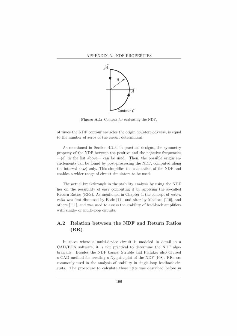
APPENDIX A. NDF PROPERTIES
R
Ā
jȀ
Contour C
Figure A.1: Contour for evaluating the NDF.
of times the NDF contour encircles the origin counterclockwise, is equal
to the number of zeros of the circuit determinant.
As mentioned in Section 4.2.3, in practical designs, the symmetry
property of the NDF between the positive and the negative frequencies
—(e) in the list above— can be used. Then, the possible origin en-
circlements can be found by post-processing the NDF, computed along
the interval [0, ω) only. This simplifies the calculation of the NDF and
enables a wider range of circuit simulators to be used.
The actual breakthrough in the stability analysis by using the NDF
lies on the possibility of easy computing it by applying the so-called
Return Ratios (RRs). As mentioned in Chapter 4, the concept of return
ratio was first discussed by Bode [11], and after by Maclean [110], and
others [111], and was used to assess the stability of feed-back amplifiers
with single- or multi-loop circuits.
A.2 Relation between the NDF and Return Ratios
(RR)
In cases where a multi-device circuit is modeled in detail in a
CAD/EDA software, it is not practical to determine the NDF alge-
braically. Besides the NDF basics, Struble and Platzker also devised
a CAD method for creating a Nyquist plot of the NDF [108]. RRs are
commonly used in the analysis of stability in single-loop feedback cir-
cuits. The procedure to calculate those RRs was described before in
196
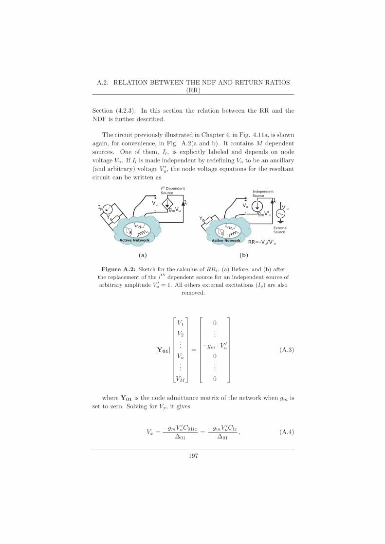
A.2. RELATION BETWEEN THE NDF AND RETURN RATIOS(RR)
Section (4.2.3). In this section the relation between the RR and the
NDF is further described.
The circuit previously illustrated in Chapter 4, in Fig. 4.11a, is shown
again, for convenience, in Fig. A.2(a and b). It contains M dependent
sources. One of them, Il, is explicitly labeled and depends on node
voltage Vu. If Il is made independent by redefining Vu to be an ancillary
(and arbitrary) voltage V ′u, the node voltage equations for the resultant
circuit can be written as
Active Network
Ip
Yp
VugmVu
ith Dependent Source
Il
(a)
Active Network
Yp
Vu
gmV'u
Independent Source
V'u
RR=-Vu/V'u
Il
ExternalSource
(b)
Figure A.2: Sketch for the calculus of RRi. (a) Before, and (b) after
the replacement of the ith dependent source for an independent source of
arbitrary amplitude V ′u = 1. All others external excitations (Ip) are also
removed.
[Y01]
⎡⎢⎢⎢⎢⎢⎢⎢⎢⎢⎢⎢⎣
V1
V2
...
Vu
...
VM
⎤⎥⎥⎥⎥⎥⎥⎥⎥⎥⎥⎥⎦=
⎡⎢⎢⎢⎢⎢⎢⎢⎢⎢⎢⎢⎣
0...
−gm · V ′u
0...
0
⎤⎥⎥⎥⎥⎥⎥⎥⎥⎥⎥⎥⎦
(A.3)
where Y01 is the node admittance matrix of the network when gm is
set to zero. Solving for Vx, it gives
Vx =−gmV ′
uC01lx
Δ01=
−gmV ′uClx
Δ01, (A.4)
197

APPENDIX A. NDF PROPERTIES
where C01lu is the co-factor of the element y01lu inY01, and Clu is the
co-factor of the element ylu in the full admittance matrix, Y. C01lu =
Clu since the only difference between Y and Y01 is the l, u element,
which does not contribute to either co-factor. Thus, it is possible to
associate a RR with the dependent source as
RR1 = −Vu
V ′u
= gmClu
Δ01, (A.5)
where Δ01 is the determinant ofY01. By applying the Laplace expan-
sion of Y along the row or the column that contains ylu, and observing
that ylu = y01lu + gm, it is possible to claim that
Δ = Δ01 + gmClu. (A.6)
Then, by replacing (A.5) into (A.6), we obtain the expression that
relates the RR with the NDF.
Δ
Δ01= 1 +RR1. (A.7)
In circuits with several dependent sources, it is possible to use a
straightforward extension of the above procedure for calculating the NDF
[108]:
NDF =Δ
Δ0(1,2,··· ,M)=
Δ
Δ0(1)· Δ0(1)
Δ0(2)· Δ0(2)
Δ0(3)· · · Δ0(M−1)
Δ0(M)
= (1 +RR1)(1 +RR2) · · · (1 +RRM ),
(A.8)
and finally, the expression shown before in (4.15):
NDF =
M∏i=1
(RRi + 1) . (A.9)
198

APPENDIX B
DESIGN AND NOISE FIGUREMEASUREMENT OF A BALANCED
NON-FOSTER IMPEDANCE
The noise added by a transistor-based non-Foster circuits to a host
structure (e.g. a filter or an antenna) is a factor of growing interest
in the microwave and antenna community. Even when such non-Foster
element is embedded into a distributed-elements circuit or in a radiating
structure, doing impossible the access to its input-output ports, the noise
characterization of the added noise is welcome. This appendix contains
the design process of a two-port balanced NIC, manufactured as a stand-
alone device, with the aim of measuring its Noise Figure (NF). The
most part of the work presented in this appendix was carried out during
a research stage at the Queen Mary University of London (QMUL),
in collaboration with members of the Antennas and Electromagnetics
Research Group, lead by Prof. Yang Hao.
B.1 NIC Topology
With the purpose of characterizing the noise performance of a stan-
dalone NIC, a couple of previous one-port prototypes, previously de-
veloped to be embedded into an antenna, are re-designed to implement

APPENDIX B. NOISE IN NON-FOSTER
a two-port device whose NF can be measured. A conventional topol-
ogy, first proposed by Linvill [19], is used because of its suitability for
two-port noise characterization. This NIC topology consists of two cross-
coupled BJT-transistors, configured in such a way a signal can be coupled
through the two-port network. Figure B.1 shows a simplified schematic
of the described NIC topology, modeled in the AWR� software. The
two resistors R2 are included to bias the BJTs and, at the same time,
to make the equivalent negative capacitance of the NIC less sensitive to
variations and parasitics in the lumped elements, as proposed in [70].
R1
R2R2
R1
P1 P2
CL
EB B
C
E
C
Q1 Q2
Figure B.1: Simplified NIC schematic for the noise figure
characterization.
An FR4 slab, with 1.5 mm thick and a relative permittivity (εr) of
4.3, is used as substrate. Two BFG410W BJT-transistors, manufactured
by NXP� semiconductors, are used to act as active devices. The man-
ufactured prototype is shown in Fig. B.2a. A touchstone file containing
the S-parameters is extracted from the network analyzer. After post-
processing, it is possible to extract the equivalent non-Foster impedance,
seen across the two-port network, as it is shown in Fig. B.2b.
As a result, the NIC impedance is no longer a constant (frequency
independent) negative capacitance but instead is a bandwidth-limited
non-constant negative capacitance, even with a negative resistive part.
Parasitics and possible differences between the active devices might be
the origin of the differences between the measured and the simulated
NIC impedance response.
200

B.1. NIC TOPOLOGY
(a) (b)
Figure B.2: (a) Prototyped 2-port NIC on a PCB. (b) Simulated and
measured response of the NIC impedance (ZNIC) showing the negative
slope of the imaginary part, proof of the non-Foster behavior.
Figure B.3 depicts the equivalent negative capacitance implemented
with the NIC, which can be computed once the measured Y21 parameter
is extracted, as in (B.1).
ZNIC = −1/Y21. (B.1)
10 60 110 160 210 260 310 360 400Frequency (MHz)
-50
-40
-30
-20
-10
0
10
20
Cap
acita
nce
(pF)
Measurement
Simulation
Range of reasonable agreement
Figure B.3: Equivalent capacitance that shows an acceptable
agreement between measurement and simulation up to 200 MHz.
A negative capacitor is obtained as far as the reactive part of the NIC
impedance (continuous blue line in Fig. B.2b) cross the zero (XNIC =
0 Ω), that is, up to about 200 MHz.
201

APPENDIX B. NOISE IN NON-FOSTER
B.2 Noise Performance Modeling
The noise contributions in the NIC can be modeled by including
the main noise sources: the shot-, the ficker-, and the burst- noise in
the BJTs, and the thermal noise associated with the lossy components.
A reasonable model for the noise in a BJT is depicted in Fig. B.4.
It includes a thermal noise voltage source associated to the resistive
component of the base; a current noise source in shunt with the junc-
tion base-emitter, accounting for the shot noise accompanying the base
current (the flicker and the burst noise are very low in bipolar transis-
tors [132]). Finally, a noise current source associated to the shot noise
in the collector. The detailed analytical noise modeling of the transistor
has been reported in [133–135].
Themal noise
Shot, Flicker (1/f )and burst (1/f2) noise
Shot noiset
B C
E
Figure B.4: Small signal model of a BJT, including the main noise
contributions [135].
Once those noise sources are included in the small signal model of the
transistors, it is possible to obtain a complete noise circuital model of
the NIC, as the one depicted in Fig. B.5. By means of a circuit simulator
with the harmonic balance simulation capability, it is possible to analyze
the NF of the NIC across its working band, in order to compare it with
the measurement, as it will be shown in the section below.
B.3 Measurements
Among the techniques for measuring noise in two-port devices, the
Y -factor is one of the most used due to its capabilities of wide frequency
range as well as the wider availability of Spectrum Analyzers (SA) as
compared to a noise figure meter. In addition, nowadays, many Noise
202

B.3. MEASUREMENTS
Figure B.5: Representation of the current and voltage noise sources in
the balanced SCS-NIC [117] used for simulating the NF response in the
AWR software. k is the Boltzmann constant (1.38 · 10−23 J/K). The
inset on the right shows the NIC schematic of Fig. B.1.
Figure Analyzers (NFA) implements this technique in an automated way
and let us account for the effects due to losses in connectors, attenuators,
matching pads, and so on, involved in the test fixture. Figure B.6 depicts
the Y -factor strategy. The Device Under Test (DUT), and any other
coupling device, have to be removed at the calibration stage. In this
technique, a calibrated noise source with a known output noise level must
be available. It is represented by the Excess Noise Ratio (ENR). The
ENR value is expressed in dB as a difference between hot temperature
(Th when noise source ON) and cold temperature (Tc when noise source
OFF), divided by the room temperature, T0, as follows
ENRDB = 10 log
(Th − Tc
T0
). (B.2)
As the instrument (NFA or SA) itself contributes to the overall noise
result, a calibration (or second stage correction) is needed. Then, by
applying the Friis formula, the Noise Factor (F) —linear scaled noise
figure— of the cascaded system, NFA + DUT is given as:
203
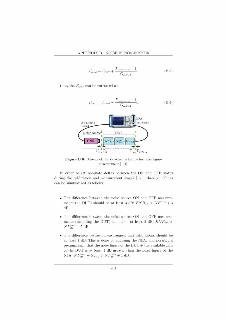
APPENDIX B. NOISE IN NON-FOSTER
Ftotal = FDUT +Finstrument − 1
GA:DUT
, (B.3)
thus, the FDUT can be extracted as
FDUT = Ftotal − Finstrument − 1
GA:DUT
. (B.4)
Figure B.6: Scheme of the Y -factor technique for noise figure
measurement [131].
In order to set adequate deltas between the ON and OFF states
during the calibration and measurement stages [136], three guidelines
can be summarized as follows:
The difference between the noise source ON and OFF measure-
ments (no DUT) should be at least 3 dB: ENRdB > NFNFA + 3
dB.
The difference between the noise source ON and OFF measure-
ments (including the DUT) should be at least 5 dB: ENRdB >
NFDUT
dB + 5 dB.
The difference between measurement and calibrations should be
at least 1 dB. This is done by choosing the NFA, and possibly a
preamp, such that the noise figure of the DUT + the available gain
of the DUT is at least 1 dB greater than the noise figure of the
NFA: NFDUT
dB +GDUT
A:dB > NFNFA
dB + 1 dB.
204
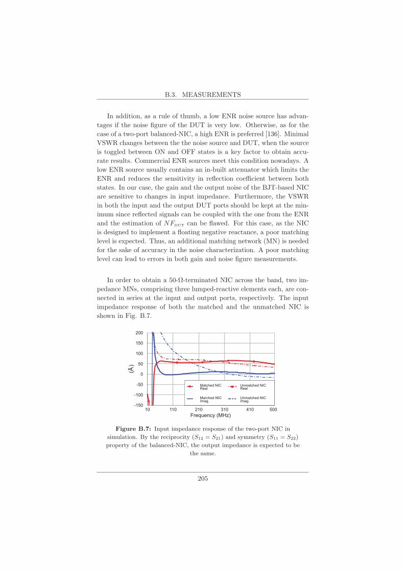
B.3. MEASUREMENTS
In addition, as a rule of thumb, a low ENR noise source has advan-
tages if the noise figure of the DUT is very low. Otherwise, as for the
case of a two-port balanced-NIC, a high ENR is preferred [136]. Minimal
VSWR changes between the the noise source and DUT, when the source
is toggled between ON and OFF states is a key factor to obtain accu-
rate results. Commercial ENR sources meet this condition nowadays. A
low ENR source usually contains an in-built attenuator which limits the
ENR and reduces the sensitivity in reflection coefficient between both
states. In our case, the gain and the output noise of the BJT-based NIC
are sensitive to changes in input impedance. Furthermore, the VSWR
in both the input and the output DUT ports should be kept at the min-
imum since reflected signals can be coupled with the one from the ENR
and the estimation of NFDUT can be flawed. For this case, as the NIC
is designed to implement a floating negative reactance, a poor matching
level is expected. Thus, an additional matching network (MN) is needed
for the sake of accuracy in the noise characterization. A poor matching
level can lead to errors in both gain and noise figure measurements.
In order to obtain a 50-Ω-terminated NIC across the band, two im-
pedance MNs, comprising three lumped-reactive elements each, are con-
nected in series at the input and output ports, respectively. The input
impedance response of both the matched and the unmatched NIC is
shown in Fig. B.7.
10 110 210 310 410 500Frequency (MHz)
-150
-100
-50
0
50
100
150
200
(Ā)
Matched NIC Real
Marched NIC Imag.
Unmatched NIC Real
Unmatched NIC Imag.
Figure B.7: Input impedance response of the two-port NIC in
simulation. By the reciprocity (S12 = S21) and symmetry (S11 = S22)
property of the balanced-NIC, the output impedance is expected to be
the same.
205

APPENDIX B. NOISE IN NON-FOSTER
The measurements were carried out following the test fixture depicted
in Fig. B.8a. A mini-anechoic chamber is used to act as a Faraday cage,
and was exclusively designed by the QMUL laboratory staff to avoid the
interference of surrounding noise. The ENR, shown in Fig. B.8b, is an
Agilent-346B with a NF of around 15 dB, characterized up to 18 GHz. A
Rohde and Schwarz FSP40 spectrum analyzer is used as instrument. An
application firmware (FSV-K30) installed in the SA provides an enor-
mous reduction in instrument noise figure (NFNFA). Such a reduction
in the instrument NF let us to avoid the use of a preamplifier to com-
pensate possible GA:DUT issues. Corrections are also applied for losses of
connectors between devices.
Noise figure meter
DC supply
Anechoic chamber
ENR + DUT
(a)
(b)
Figure B.8: (a) Noise figure measurement setup and (b) a zoom
showing the ENR and the NIC.
The measured NF along with the simulated results are shown in Fig.
B.9. A difference within the range 5 dB to 9 dB is observed, being
206
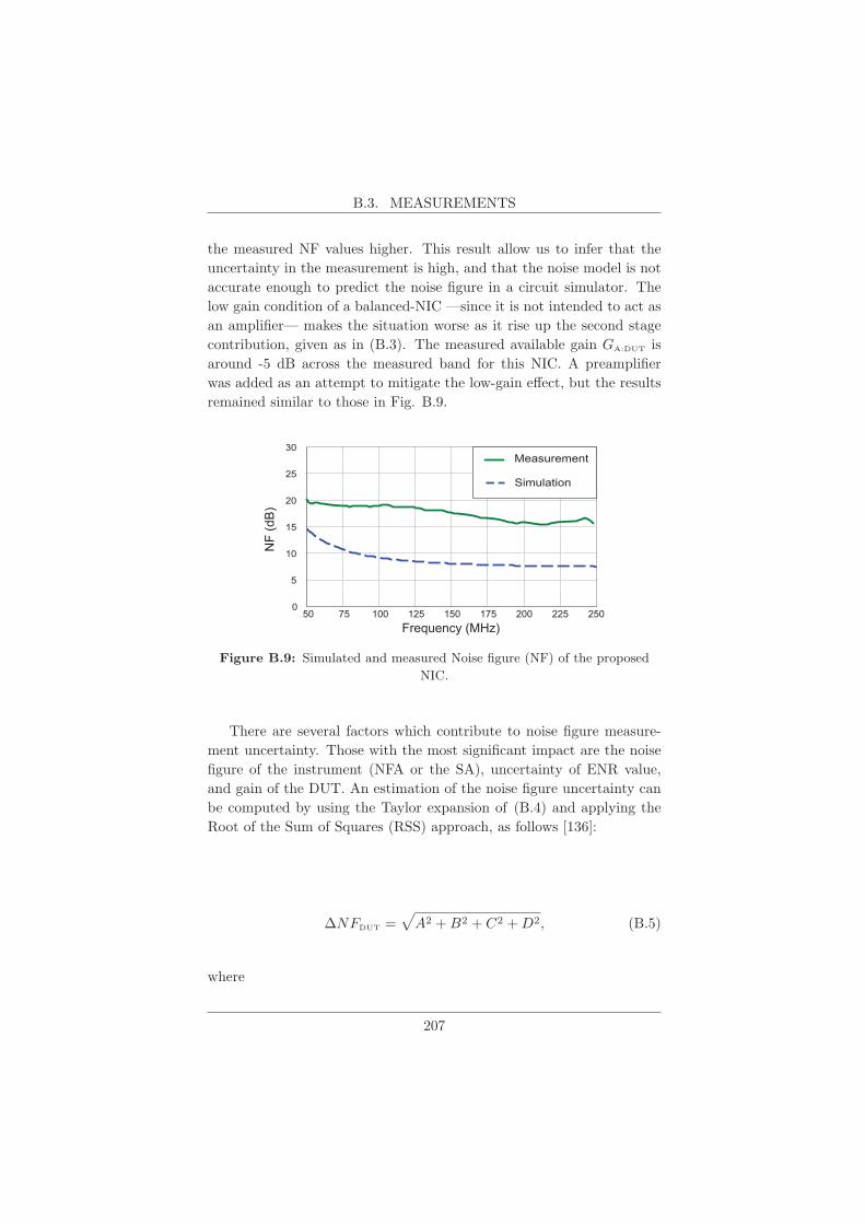
B.3. MEASUREMENTS
the measured NF values higher. This result allow us to infer that the
uncertainty in the measurement is high, and that the noise model is not
accurate enough to predict the noise figure in a circuit simulator. The
low gain condition of a balanced-NIC —since it is not intended to act as
an amplifier— makes the situation worse as it rise up the second stage
contribution, given as in (B.3). The measured available gain GA:DUT is
around -5 dB across the measured band for this NIC. A preamplifier
was added as an attempt to mitigate the low-gain effect, but the results
remained similar to those in Fig. B.9.
0
5
10
15
20
25
30Measurement
Simulation
50 75 100 125 150 175 200 225 250Frequency (MHz)
NF
(dB
)
Figure B.9: Simulated and measured Noise figure (NF) of the proposed
NIC.
There are several factors which contribute to noise figure measure-
ment uncertainty. Those with the most significant impact are the noise
figure of the instrument (NFA or the SA), uncertainty of ENR value,
and gain of the DUT. An estimation of the noise figure uncertainty can
be computed by using the Taylor expansion of (B.4) and applying the
Root of the Sum of Squares (RSS) approach, as follows [136]:
ΔNFDUT =√A2 +B2 + C2 +D2, (B.5)
where
207
APPENDIX B. NOISE IN NON-FOSTER
A =Ftotal
FDUT
ΔNFtotal,dB,
B =FNFA
FDUTGA:DUT
ΔNFNFA,dB,
C =Ftotal − 1
FDUTGA:DUT
ΔGA:DUT,dB,
D =
(Ftotal
FDUT
− FNFA
FDUTGA:DUT
)ΔENRdB.
(B.6)
The four delta terms in the previous equations accounts for the four
“primary contributions” of measurement uncertainty. The ΔENRdB
is specified by the manufacturer and is around 0.2 dB for this case.
The remaining three delta terms are strong functions of the reflection
coefficients at both the DUT input (Γin) and output (Γout) ports, at the
NFA/SA input (Γin:NFA), and at the ENR port (Γs). The NFAuncert:dB
values are typically around 0.05 dB in commercial instruments. The
three remaining delta terms can be computed as
ΔNFtotal,dB =
√(20 log(1− ΓsΓin))
2+ (NFAuncert:dB)
2, (B.7)
ΔNFNFA,dB =
√(20 log(1− ΓsΓin:NFA))
2+ (NFAuncert:dB)
2, (B.8)
ΔGA:DUT,dB =
√√√√ (20 log(1− ΓsΓin:NFA))2+ (20 log(1− ΓsΓin))
2
+ (20 log(1− ΓoutΓNFA:in))2+ (NFAuncert:dB)
2.
(B.9)
Some manufacturers provide designers with open-access applets
specifically devoted to calculate the uncertainty in the noise figure mea-
surement. Figures B.10(a, b) shows a theoretical analysis of the mea-
surement uncertainty for the used equipment, as a function of the NFDUT
and its gain, according to (B.5). It is assumed that the cascaded noise
figure (NFtotal) equalsNFDUT as the firmware FSV-K30 reduces the noise
figure of the SA to a very low value across the working band. Two dif-
ferent matching levels at the DUT ports were analyzed. Even with an
acceptable matching level (V SWR = 2), at each DUT port, the noise
208
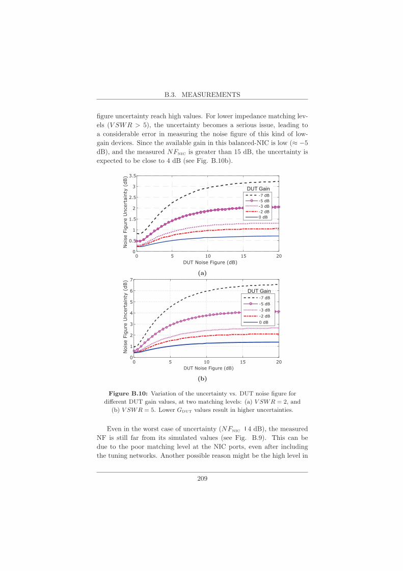
B.3. MEASUREMENTS
figure uncertainty reach high values. For lower impedance matching lev-
els (V SWR > 5), the uncertainty becomes a serious issue, leading to
a considerable error in measuring the noise figure of this kind of low-
gain devices. Since the available gain in this balanced-NIC is low (≈ −5
dB), and the measured NFNIC is greater than 15 dB, the uncertainty is
expected to be close to 4 dB (see Fig. B.10b).
DUT Noise Figure (dB)0 5 10 15 20
Noi
se F
igur
e U
ncer
tain
ty (
dB)
0
0.5
1
1.5
2
2.5
3
3.5
-7 dB-5 dB-3 dB-2 dB0 dB
DUT Gain
(a)
DUT Noise Figure (dB)0 5 10 15 20
Noi
se F
igur
e U
ncer
tain
ty (
dB)
0
1
2
3
4
5
6
7
-7 dB-5 dB-3 dB-2 dB0 dB
DUT Gain
(b)
Figure B.10: Variation of the uncertainty vs. DUT noise figure for
different DUT gain values, at two matching levels: (a) V SWR = 2, and
(b) V SWR = 5. Lower GDUT values result in higher uncertainties.
Even in the worst case of uncertainty (NFNIC 4 dB), the measured
NF is still far from its simulated values (see Fig. B.9). This can be
due to the poor matching level at the NIC ports, even after including
the tuning networks. Another possible reason might be the high level in
209

APPENDIX B. NOISE IN NON-FOSTER
noise figure of the proposed two-port NIC, whose value is close to that of
the ENR level itself. This is not an advisable condition for the Y -factor
technique to be applied, as mentioned before. Further considerations on
the accuracy in noise figure evaluation of low-gain mismatched devices
through the Y -factor approach are presented in [137]. It was found
that errors in the noise are mainly related to the fact of neglecting the
DUT mismatch effect on the noise figure of the instrument (NFA or SA).
Furthermore, the use of the available gain, GA:DUT, instead of insertion
gain does not necessarily provide more accurate results for high values
of DUT return losses.
B.4 Conclusion
A two-port non-Foster impedance implemented with a balanced BJT-
based NIC has been shown. It has been measured and reported to work
from 50 MHz to 200 MHz, acting as a negative capacitor. The noise fig-
ure measurement has been done by applying the Y -factor technique. An
additional input-output MNs were included to obtain a 50-Ω-terminated
two-port network, as necessary for the Y -factor approach. The device
noise figure is between 15 to 20 dB, across the band 50 MHz to 250 MHz.
The noise figure uncertainty has been also estimated. This specific NIC
circuit has been found to be a “noisy” device. Thus, more efforts have
to be made to reduce its noise figure of merit to lower values, as they
has been found by other authors, whose measured NFDUT is between 10
to 15 dB [138].
In addition, from the actively matched ESA point of view, in spite
that the non-Foster MNs have provided enormous bandwidth improve-
ments, their significantly high noise figure —as for the BJT-based NIC
shown here— indicates a source for degradation in the receiving mode.
Thus, an additional tradeoff between the output SNR and the impedance
bandwidth is also present in the actively matched ESA design, loaded
with non-Foster elements.
210

PUBLICATIONS
The work developed in this Ph.D. thesis has led to journal and con-
ference contributions. The complete list is detailed below.
Journals
Related with Chapter 3:
F. Albarracın-Vargas, E. Ugarte Munoz, and D. Segovia Var-
gas, “Sensitivity analysis for active matched antennas with non-
Foster elements,” IEEE Transactions on Antennas and Propaga-
tion, vol. 62, no. 12, pp. 6040–6048, Dec. 2014.
Related with Chapter 4:
F. Albarracın-Vargas, V. G. Posadas, F. J. Herraiz-Martinez, and
D. Segovia-Vargas, “Design Method for Actively Matched Anten-
nas with Non-Foster Elements,” IEEE Transactions on Antennas
and Propagation, vol. PP, no. 99, pp. 1–1, Jun. 2016.
D. Segovia-Vargas, J. L. Jimenez-Martin, A. Parra-Cerrada,
E. Ugarte-Munoz, L. F. Albarracın-Vargas, and V. Gonzalez-
Posadas, “Stability Analysis and Design of Negative Impedance
Converters: application to circuit and small antennas,” Radioengi-
neering, vol. 25, no. 3, pp. 409–418, Sep. 2016.

PUBLICATIONS
Related with Chapter 5:
F. Albarracın-Vargas and D. Segovia-Vargas, “Active Non-Foster
Matching Network for a Small Printed Antenna Array,” IEEE An-
tennas and Wireless Propagation Letters, no. submitted, 2017.
Related with Appendix B:
F. Albarracın-Vargas, D. S. Nagarkoti, and D. Segovia-Vargas,
“Noise Measurements in a Balanced Two-Port Negative Impedance
Converter,” IEEE Transactions on Microwave Theory and Tech-
niques, no. submitted, 2017.
Conferences
Related with Chapter 3:
F. Albarracın-Vargas, E. Ugarte Munoz, V. Gonzlez Posadas, and
D. Segovia Vargas, “Consideraciones de diseo de adaptacin activa
para antenas cargadas con circuitos non-Foster,” in XXIX Sim-
posium nacional de la URSI, Valencia 2014, Valencia, 2014, pp.
1–4.
E. Ugarte-Munoz, F. Albarracın-Vargas, F. Herraiz-Martinez, and
D. Segovia-Vargas, “Sensitivity and stability analysis of non-foster
matched two-port antennas,” in 2013 7th European Conference on
Antennas and Propagation (EuCAP), Apr. 2013, pp. 3006–3009.
E. Ugarte Munoz, F. Albarracın-Vargas, and D. Segovia Var-
gas, “Anlisis de Sensibilidad de Antenas Adaptadas con Redes de
Adaptacin non-Foster,” in XXVIII Symposium of the International
Union of Radio Science, URSI 2013, Spain, Sep. 2013.
F. Albarracın-Vargas, E. Ugarte Munoz, and D. Segovia Vargas,
“Design Considerations on Active Matching for Small Antennas
with Non-Foster Forms,” in 2014 8th International Congress on
Advanced Electromagnetic Materials in Microwaves and Optics
(METAMATERIALS), Aug. 2014.
212

A. Lopez-Yela, F. Albarracın-Vargas, and D. Segovia Vargas, “Pas-
sive Matching Networks for Electrically Small Antennas,” in XXX
Symposium of the International Union of Radio Science, URSI
2015, Spain, Sep. 2015.
related with Chapter 4
F. Albarracın-Vargas and D. Segovia-Vargas, “A printed monopole
loaded with a non-Foster matching network in the VHF band;
radiation considerations,” in 2015 9th International Congress on
Advanced Electromagnetic Materials in Microwaves and Optics
(METAMATERIALS), Sep. 2015, pp. 7–9.
F. Albarracın-Vargas, E. Ugarte-Munoz, V. Gonzalez-Posadas, and
D. Segovia-Vargas, “A design strategy of active matched small-
antennas with non-Foster elements,” in 2015 9th European Con-
ference on Antennas and Propagation (EuCAP), Apr. 2015, pp.
1–4.
F. Albarracın-Vargas, D. Segovia-Vargas, and V. Gonzalez-
Posadas, “Non-Foster matching network for a small, bladetype
monopole in the VHF band,” in 2015 IEEE International Sympo-
sium on Antennas and Propagation USNC/URSI National Radio
Science Meeting, Jul. 2015, pp. 1396–1397.
A. Lopez-Yela, F. Albarracın-Vargas, F. Herraiz-Martinez,
D. Segovia-Vargas, and V. Gonzalez-Posadas, “Embedded match-
ing networks for electrically small antennas,” in 2016 10th Eu-
ropean Conference on Antennas and Propagation (EuCAP), Apr.
2016, pp. 1–4.
related with Chapter 5
F. Albarracın-Vargas, D. Segovia-Vargas, and V. Gonzalez-
Posadas, “Design considerations in an active matched semiloop
array with non-foster networks,” in 2016 IEEE International Sym-
posium on Antennas and Propagation (APSURSI), Jun. 2016, pp.
925–926.
213

PUBLICATIONS
F. Albarracın-Vargas, F. J. Herraiz-Martinez, and D. Segovia-
Vargas, “Small Printed Log-Periodic Array, Matched with an Ac-
tive non-Foster Network,” in 2017 11th European Conference on
Antennas and Propagation (EuCAP), Apr. 2017, pp. 1–4.
E. Ugarte-Munoz, S. Hrabar, D. Segovia-Vargas, and A. Kiricenko,
“Stability of Non-Foster Reactive Elements for Use in Active Meta-
materials and Antennas,” IEEE Transactions on Antennas and
Propagation, vol. 60, no. 7, pp. 3490–3494, Jul. 2012.
214

BIBLIOGRAPHY
[1] C. A. Balanis, Modern Antenna Handbook. John Wiley & Sons,
Sep. 2011.
[2] R. C. Hansen and R. E. Collin, Small Antenna Handbook. John
Wiley & Sons, Aug. 2011.
[3] K. Fujimoto and H. Morishita, Modern Small Antennas. Cam-
bridge University Press, Jan. 2014.
[4] J. Volakis, C.-C. Chen, and K. Fujimoto, Small Antennas: Minia-
turization Techniques & Applications, ser. pp. 361-388. McGraw
Hill Professional, Dec. 2009.
[5] R. C. Hansen, “Fundamental limitations in antennas,” Proceedings
of the IEEE, vol. 69, no. 2, pp. 170–182, Feb. 1981.
[6] Halton Company, “Halton Garage Door Opener,” http://www.
haltongaragedoors.ca/, Apr. 2017.
[7] 3M Company, “RFID Products,” http://solutions.3m.com/wps/
portal/3M/en WW/Track Trace/home/Products/one/one/, Apr.
2017.

[8] B. D. Pell, E. Sulic, W. S. Rowe, K. Ghorbani, and S. John, “Ad-
vancements in automotive antennas,” New Trends and Develop-
ments in Automotive System Engineering, 2011.
[9] Cobham Company, “UHF/L Band Communication Antenna,”
http://www.cobham.com/communications-and-connectivity/
antenna-systems/, Apr. 2016.
[10] H. A. Wheeler, “Fundamental limitations of small antennas,” Pro-
ceedings of the IRE, vol. 35, no. 12, pp. 1479–1484, Dec. 1947.
[11] H. W. Bode, Network Analysis and Feedback Amplifier Design.
Van Nostrand, 1945.
[12] R. M. Fano, Theoretical Limitations on the Broadband Matching
of Arbitrary Impedances. MIT Res. Lab. of Electronics, 1947.
[13] L. J. Chu, “Physical limitations of omni-directional antennas,”
Journal of applied physics, vol. 19, no. 12, pp. 1163–1175, Dec.
1948.
[14] R. F. Harrington, “Effect of antenna size on gain, bandwidth, and
efficiency,” J. Res. Nat. Bur. Stand, vol. 64, no. 1, pp. 1–12, 1960.
[15] S. Best, “Low Q electrically small linear and elliptical polarized
spherical dipole antennas,” IEEE Transactions on Antennas and
Propagation, vol. 53, no. 3, pp. 1047–1053, Mar. 2005.
[16] D. Youla, “A New Theory of Broad-band Matching,” IEEE Trans-
actions on Circuit Theory, vol. 11, no. 1, pp. 30–50, Mar. 1964.
[17] H. L. Thal, “New Radiation Limits for Spherical Wire Antennas,”
IEEE Transactions on Antennas and Propagation, vol. 54, no. 10,
pp. 2757–2763, Oct. 2006.
[18] R. M. Foster, “A reactance theorem,” Bell System Technical Jour-
nal, The, vol. 3, no. 2, pp. 259–267, Apr. 1924.
[19] J. Linvill, “Transistor Negative-Impedance Converters,” Proceed-
ings of the IRE, vol. 41, no. 6, pp. 725–729, Jun. 1953.
[20] K. L. Su, “A Method for Realizing the Negative-Impedance In-
verter,” IEEE Journal of Solid-State Circuits, vol. 2, no. 1, pp.
22–25, Mar. 1967.
216

[21] T. Yanagisawa, “RC Active Networks Using Current Inversion
Type Negative Impedance Converters,” IRE Transactions on Cir-
cuit Theory, vol. 4, no. 3, pp. 140–144, Sep. 1957.
[22] A. Davies, “Stability Properties of a Negative Immittance Con-
verter,” IEEE Transactions on Circuit Theory, vol. 15, no. 1, pp.
80–81, Mar. 1968.
[23] S. Kolev, B. Delacressonniere, and J.-L. Gautier, “Using a nega-
tive capacitance to increase the tuning range of a varactor diode
in MMIC technology,” Microwave Theory and Techniques, IEEE
Transactions on, vol. 49, no. 12, pp. 2425–2430, 2001.
[24] C. A. Balanis, Antenna theory: analysis and design, 3rd ed. Hobo-
ken, NJ: John Wiley, 2005.
[25] W. L. Stutzman and G. A. Thiele, Antenna Theory and Design,
3rd ed. John Wiley & Sons, May 2012.
[26] J. D. Kraus and R. J. Marhefka, Antennas for all applications.
McGraw-Hill, 2002.
[27] P.-S. Kildal, Foundations of Antenna Engineering: A Unified Ap-
proach for Line-of-sight and Multipath. Artech House Publishers,
2015.
[28] R. W. P. King, The theory of linear antennas: with charts and
tables for practical applications. Harvard University Press, 1956.
[29] O. Lodge, Signalling Across Space Without Wires: Being a De-
scription of the Work of Hertz and His Successors. Cambridge
University Press, Mar. 2013.
[30] D. F. Sievenpiper, D. C. Dawson, M. M. Jacob, T. Kanar, S. Kim,
J. Long, and R. G. Quarfoth, “Experimental Validation of Perfor-
mance Limits and Design Guidelines for Small Antennas,” IEEE
Transactions on Antennas and Propagation, vol. 60, no. 1, pp. 8–
19, Jan. 2012.
[31] J. S. McLean, “A re-examination of the fundamental limits on the
radiation Q of electrically small antennas,” IEEE Transactions on
Antennas and Propagation, vol. 44, no. 5, pp. 672–, May 1996.
217

[32] R. Collin and S. Rothschild, “Evaluation of antenna Q,” IEEE
Transactions on Antennas and Propagation, vol. 12, no. 1, pp. 23–
27, Jan. 1964.
[33] W. Geyi, P. Jarmuszewski, and Y. Qi, “The Foster reactance the-
orem for antennas and radiation Q,” IEEE Transactions on An-
tennas and Propagation, vol. 48, no. 3, pp. 401–408, Mar. 2000.
[34] D. M. Pozar, Microwave Engineering, 2nd ed. Wiley, Aug. 1998.
[35] R. C. Hansen, “Bode and Fano impedance matching,” Microwave
and Optical Technology Letters, vol. 50, no. 4, pp. 875–877, Apr.
2008.
[36] H. Mirzaei and G. V. Eleftheriades, “A Compact Frequency-
Reconfigurable Metamaterial-Inspired Antenna,” IEEE Antennas
and Wireless Propagation Letters, vol. 10, pp. 1154–1157, 2011.
[37] M. C. Tang, R. W. Ziolkowski, S. Xiao, M. Li, and
J. Zhang, “Frequency-Agile, Efficient, Near-Field Resonant Par-
asitic Monopole Antenna,” IEEE Transactions on Antennas and
Propagation, vol. 62, no. 3, pp. 1479–1483, Mar. 2014.
[38] N. Zhu and R. W. Ziolkowski, “Active Metamaterial-Inspired
Broad-Bandwidth, Efficient, Electrically Small Antennas,” IEEE
Antennas and Wireless Propagation Letters, vol. 10, pp. 1582–
1585, 2011.
[39] S. E. Sussman-Fort and R. M. Rudish, “Non-Foster Impedance
Matching of Electrically-Small Antennas,” IEEE Transactions on
Antennas and Propagation, vol. 57, no. 8, pp. 2230–2241, Aug.
2009.
[40] D. S. Nagarkoti, K. Z. Rajab, and Y. Hao, “Design and stability of
negative impedance circuits for non-foster matching of a monopole
antenna,” in The 8th European Conference on Antennas and Prop-
agation (EuCAP 2014), Apr. 2014, pp. 2707–2709.
[41] C. R. White, J. S. Colburn, and R. G. Nagele, “A Non-Foster VHF
Monopole Antenna,” IEEE Antennas and Wireless Propagation
Letters, vol. 11, pp. 584–587, 2012.
218

[42] H. Mirzaei and G. V. Eleftheriades, “A Resonant Printed
Monopole Antenna With an Embedded Non-Foster Matching Net-
work,” IEEE Transactions on Antennas and Propagation, vol. 61,
no. 11, pp. 5363–5371, Nov. 2013.
[43] W. Wang, J. Geng, R. Jin, X. Liang, and R. Ziolkowski, “Design of
a 600 MHz non-Foster dipole,” in 2014 International Workshop on
Antenna Technology: ”Small Antennas, Novel EM Structures and
Materials, and Applications” (iWAT), Mar. 2014, pp. 351–354.
[44] M. Barbuto, A. Monti, F. Bilotti, and A. Toscano, “De-
sign of a Non-Foster Actively Loaded SRR and Application in
Metamaterial-Inspired Components,” IEEE Transactions on An-
tennas and Propagation, vol. 61, no. 3, pp. 1219–1227, Mar. 2013.
[45] O. O. Tade, P. Gardner, and P. S. Hall, “Antenna bandwidth
broadening with a negative impedance converter,” International
Journal of Microwave and Wireless Technologies, vol. 5, no. Spe-
cial Issue 03, pp. 249–260, Jun. 2013.
[46] C. D. Nallo, G. Bit-Babik, and A. Faraone, “Wideband an-
tenna using non-foster loading elements,” in 2007 IEEE Antennas
and Propagation Society International Symposium, Jun. 2007, pp.
4501–4504.
[47] M. C. Tang, H. Wang, T. Deng, and R. Ziolkowski, “Compact
Planar Ultra-wideband Antennas with Continuously Tunable, In-
dependent Band-Notched Filters,” IEEE Transactions on Anten-
nas and Propagation, vol. PP, no. 99, pp. 1–1, 2016.
[48] F. J. Herraiz-Martinez, P. S. Hall, Q. Liu, and D. Segovia-Vargas,
“Left-Handed Wire Antennas Over Ground Plane With Wide-
band Tuning,” IEEE Transactions on Antennas and Propagation,
vol. 59, no. 5, pp. 1460–1471, May 2011.
[49] S. k. Oh, Y. s. Shin, and S. o. Park, “A novel PIFA type varactor
tunable antenna with U-shaped slot,” in 2006 7th International
Symposium on Antennas, Propagation EM Theory, Oct. 2006, pp.
1–3.
[50] M. Berg, M. Komulainen, V. Palukuru, H. Jantunen, and E. Salo-
nen, “Frequency-tunable DVB-H antenna for mobile terminals,” in
219

2007 IEEE Antennas and Propagation Society International Sym-
posium, Jun. 2007, pp. 1072–1075.
[51] V. A. Nguyen, R. A. Bhatti, and S. O. Park, “A Simple PIFA-
Based Tunable Internal Antenna for Personal Communication
Handsets,” IEEE Antennas and Wireless Propagation Letters,
vol. 7, pp. 130–133, 2008.
[52] N. Behdad and K. Sarabandi, “Dual-band reconfigurable antenna
with a very wide tunability range,” IEEE Transactions on Anten-
nas and Propagation, vol. 54, no. 2, pp. 409–416, Feb. 2006.
[53] I. Carrasquillo-Rivera, R. A. R. Solis, and J. G. Colom-Ustariz,
“Tunable and dual-band rectangular slot-ring antenna,” in IEEE
Antennas and Propagation Society Symposium, 2004., vol. 4, Jun.
2004, pp. 4308–4311 Vol.4.
[54] F. Costa, A. Monorchio, S. Talarico, and F. M. Valeri, “An Ac-
tive High-Impedance Surface for Low-Profile Tunable and Steer-
able Antennas,” IEEE Antennas and Wireless Propagation Letters,
vol. 7, pp. 676–680, 2008.
[55] Y. Cai, Y. J. Guo, and A. R. Weily, “A Frequency-Reconfigurable
Quasi-Yagi Dipole Antenna,” IEEE Antennas and Wireless Prop-
agation Letters, vol. 9, pp. 883–886, 2010.
[56] M. Fallahpour, M. T. Ghasr, and R. Zoughi, “Miniaturized Recon-
figurable Multiband Antenna For Multiradio Wireless Communi-
cation,” IEEE Transactions on Antennas and Propagation, vol. 62,
no. 12, pp. 6049–6059, Dec. 2014.
[57] A. Petosa, “Frequency agile antennas for wireless communications
- A survey,” in 2010 14th International Symposium on Antenna
Technology and Applied Electromagnetics the American Electro-
magnetics Conference, Jul. 2010, pp. 1–4.
[58] J. T. Aberle and R. Loepsinger-Romak, Antennas with Non-Foster
Matching Networks. Morgan & Claypool Publishers, 2007.
[59] M. E. Pedinoff, “The Negative-Conductance Slot Amplifier,” IRE
Transactions on Microwave Theory and Techniques, vol. 9, no. 6,
pp. 557–566, Nov. 1961.
220

[60] D. S. Nagarkoti, Y. Hao, D. P. Steenson, L. Li, E. H. Linfield, and
K. Z. Rajab, “Design of Broadband Non-Foster Circuits Based on
Resonant Tunneling Diodes,” IEEE Antennas and Wireless Prop-
agation Letters, vol. 15, pp. 1398–1401, 2016.
[61] J. L. Merrill, “Theory of the negative impedance converter,” The
Bell System Technical Journal, vol. 30, no. 1, pp. 88–109, Jan.
1951.
[62] A. Larky, “Negative-Impedance Converters,” IRE Transactions on
Circuit Theory, vol. 4, no. 3, pp. 124–131, Sep. 1957.
[63] C.-K. Kuo and K. Su, “Some New Four-Terminal NIC Circuits,”
IEEE Transactions on Circuit Theory, vol. 16, no. 3, pp. 379–381,
Aug. 1969.
[64] S. E. Sussman-Fort, “Gyrator-based biquad filters and negative
impedance converters for microwaves,” International Journal of
RF and Microwave Computer-Aided Engineering, vol. 8, no. 2, pp.
86–101, Mar. 1998.
[65] A. K. Perry, “Broadband Antenna Systems Realized from Ac-
tive Circuit Conjugate Impedance Matching,” Naval Postgraduate
School Monterrey CA, Tech. Rep., Sep. 1973.
[66] E. A. Gonzalez, L. Dorcak, I. Petras, and J. Terpak, “On the
mathematical properties of generalized fractional-order two-port
networks using hybrid parameters,” in Proceedings of the 14th In-
ternational Carpathian Control Conference (ICCC), May 2013, pp.
88–93.
[67] S. Kolev, B. Delacressonniere, and J. L. Gautier, “Novel Microwave
Negative Capacitance. Application to a Wide-Range Tunable Ca-
pacitance,” in Microwave Conference, 2000. 30th European, Oct.
2000, pp. 1–3.
[68] S. K. Mitra, “Alternate realizations of four-terminal and three-
terminal negative-impedance inverters,” Proceedings of the IEEE,
vol. 56, no. 3, pp. 368–368, Mar. 1968.
[69] S. Hrabar, I. Krois, and A. Kiricenko, “Towards active dispersion-
less ENZ metamaterial for cloaking applications,” Metamaterials,
vol. 4, no. 2–3, pp. 89–97, Aug. 2010.
221

[70] J. Long, M. M. Jacob, and D. F. Sievenpiper, “Broadband Fast-
Wave Propagation in a Non-Foster Circuit Loaded Waveguide,”
IEEE Transactions on Microwave Theory and Techniques, vol. 62,
no. 4, pp. 789–798, Apr. 2014.
[71] J. Long and D. F. Sievenpiper, “Low-Profile and Low-Dispersion
Artificial Impedance Surface in the UHF Band Based on Non-
Foster Circuit Loading,” IEEE Transactions on Antennas and
Propagation, vol. 64, no. 7, pp. 3003–3010, Jul. 2016.
[72] S. Hrabar, I. Krois, I. Bonic, and A. Kiricenko, “Basic concepts of
active dispersionless metamaterial based on non-foster elements,”
in ICECom, 2010 Conference Proceedings, Sep. 2010, pp. 1–4.
[73] H. Mirzaei and G. Eleftheriades, “Arbitrary-Angle Squint-Free
Beamforming in Series-Fed Antenna Arrays Using Non-Foster El-
ements Synthesized by Negative-Group-Delay Networks,” IEEE
Transactions on Antennas and Propagation, vol. 63, no. 5, pp.
1997–2010, May 2015.
[74] T. P. Weldon, J. M. C. Covington, K. L. Smith, and R. S.
Adams, “Performance of digital discrete-time implementations of
non-Foster circuit elements,” in 2015 IEEE International Sympo-
sium on Circuits and Systems (ISCAS), May 2015, pp. 2169–2172.
[75] A. D. Harris and G. A. Myers, An Investigation of Broadband
Miniature Antennas. Defense Technical Information Center, 1968.
[76] G. Skahill, R. M. Rudish, and J. A. Pierro, “Apparatus and
method for broadband matching of electrically small antennas,”
U.S. Patent US6 121 940 A, Sep., 2000.
[77] S. E. Sussman-Fort and R. Rudish, “Progress in use of non-Foster
impedances to match electrically-small antennas and arrays,” in
29th Antenna Application Symposium, Allerton Park, IL, Sep.
2005.
[78] R. M. Rudish and S. E. Sussman-Fort, “Non-foster impedance
matching improves S/N of wideband electrically-small VHF an-
tennas and arrays,” in Antenna Applications Symposium, M. H.
Hamza, Ed. Anaheim: Acta Press Anaheim, Sep. 2005.
222

[79] S. E. Sussman-Fort, “Matching network design using non-
Foster impedances,” International Journal of RF and Microwave
Computer-Aided Engineering, vol. 16, no. 2, pp. 135–142, Mar.
2006.
[80] S. E. Sussman-Fort and R. M. Rudish, “Non-Foster matching of a
lossy electrically-small antenna over an extended frequency range,”
in Antenna Applications Symposium, Allerton Park, IL, Sep. 2007.
[81] S. E. Sussman-Fort and R. Rudish, “Non-Foster Impedance Match-
ing for Transmit Applications,” in IEEE International Workshop
on Antenna Technology Small Antennas and Novel Metamaterials,
2006., White Plains, NY, Mar. 2006, pp. 53–56.
[82] Y. Fan, K. Rajab, M. Munoz, and Y. Hao, “Electrically small half-
loop antenna design with non-foster matching networks,” in 2012
6th European Conference on Antennas and Propagation (EUCAP),
Mar. 2012, pp. 126–129.
[83] K.-S. Song and R. Rojas, “Non-Foster impedance matching of elec-
trically small antennas,” in 2010 IEEE Antennas and Propagation
Society International Symposium (APSURSI), Jul. 2010, pp. 1–4.
[84] N. Zhu and R. W. Ziolkowski, “Broad-Bandwidth, Electrically
Small Antenna Augmented With an Internal Non-Foster Element,”
IEEE Antennas and Wireless Propagation Letters, vol. 11, pp.
1116–1120, 2012.
[85] J. Volakis, C.-C. Chen, and K. Fujimoto, “Chapter 8,” in Small
Antennas: Miniaturization Techniques & Applications. McGraw
Hill Professional, Dec. 2009, pp. 361–388.
[86] S. Koulouridis, “Non - foster circuitry design for antennas,” in Pro-
ceedings of the 5th European Conference on Antennas and Propa-
gation (EUCAP), Apr. 2011, pp. 237–239.
[87] E. Ugarte-Munoz, S. Hrabar, D. Segovia-Vargas, and A. Kiricenko,
“Stability of Non-Foster Reactive Elements for Use in Active Meta-
materials and Antennas,” IEEE Transactions on Antennas and
Propagation, vol. 60, no. 7, pp. 3490–3494, Jul. 2012.
223

[88] A. D. Yaghjian and S. R. Best, “Impedance, bandwidth, and Q
of antennas,” IEEE Transactions on Antennas and Propagation,
vol. 53, no. 4, pp. 1298–1324, Apr. 2005.
[89] W. L. Langston and D. R. Jackson, “Impedance, axial-ratio, and
receive-power bandwidths of microstrip antennas,” in IEEE An-
tennas and Propagation Society International Symposium, 2002,
vol. 2, 2002, pp. 882–885 vol.2.
[90] F. J. Herraiz-Martinez, V. Gonzalez-Posadas, L. E. Garcia-Munoz,
and D. Segovia-Vargas, “Multifrequency and Dual-Mode Patch
Antennas Partially Filled With Left-Handed Structures,” IEEE
Transactions on Antennas and Propagation, vol. 56, no. 8, pp.
2527–2539, Aug. 2008.
[91] M. M. Jacob, J. Long, and D. F. Sievenpiper, “Broadband non-
Foster matching of an electrically small loop antenna,” in Proceed-
ings of the 2012 IEEE International Symposium on Antennas and
Propagation, Jul. 2012, pp. 1–2.
[92] A. Sedra and K. Smith, Microelectronic Circuits. Oxford Univer-
sity Press, Incorporated, Sep. 1998.
[93] O. O. Tade, “Negative impedance converter for antenna match-
ing,” Thesis, University of Birmingham, Jul. 2014.
[94] S. D. Stearns, “Stable band-pass non-Foster circuits,” in 2015
IEEE International Symposium on Antennas and Propagation
USNC/URSI National Radio Science Meeting, Jul. 2015, pp. 1386–
1387.
[95] A. Suarez and R. Quere, Stability Analysis of Nonlinear Microwave
Circuits. Artech House, 2003.
[96] J. Brownlie, “On the Stability Properties of a Negative Impedance
Converter,” IEEE Transactions on Circuit Theory, vol. 13, no. 1,
pp. 98–99, Mar. 1966.
[97] R. F. Hoskins, “Stability of negative-impedance convertors,” Elec-
tronics Letters, vol. 2, no. 9, pp. 341–341, Sep. 1966.
[98] J. D. Brownlie, “Small-signal responses realizable from d.c.-biased
devices,” Proceedings of the Institution of Electrical Engineers, vol.
110, no. 5, pp. 823–829, May 1963.
224

[99] A. P. Stern, “Stability and Power Gain of Tuned Transistor Am-
plifiers,” Proceedings of the IRE, vol. 45, no. 3, pp. 335–343, Mar.
1957.
[100] R. D. Middlebrook, “Measurement of loop gain in feedback sys-
tems�,” International Journal of Electronics Theoretical and Ex-
perimental, vol. 38, no. 4, pp. 485–512, 1975.
[101] H. Nyquist, “Regeneration theory,” The Bell System Technical
Journal, vol. 11, no. 1, pp. 126–147, 1932.
[102] S. D. Stearns, “Circuit stability theory for non-Foster circuits,” in
Microwave Symposium Digest (IMS), 2013 IEEE MTT-S Interna-
tional. IEEE, 2013, pp. 1–3.
[103] J. Rollett, “Stability and Power-Gain Invariants of Linear
Twoports,” IRE Transactions on Circuit Theory, vol. 9, no. 1,
pp. 29–32, Mar. 1962.
[104] M. L. Edwards and J. H. Sinsky, “A new criterion for linear 2-port
stability using a single geometrically derived parameter,” IEEE
Transactions on Microwave Theory and Techniques, vol. 40, no. 12,
pp. 2303–2311, 1992.
[105] R. W. Jackson, “Rollett proviso in the stability of linear microwave
circuits-a tutorial,” IEEE Transactions on Microwave Theory and
Techniques, vol. 54, no. 3, pp. 993–1000, Mar. 2006.
[106] E. Ugarte-Munoz, D. Segovia-Vargas, V. Gonzalez-Posadas, and
J. Jimenez-Martin, “Non-Foster matching of Electrically Small
Antennas. Stability considerations,” in 2012 IEEE Antennas and
Propagation Society International Symposium (APSURSI), Jul.
2012, pp. 1–2.
[107] A. Platzker, W. Struble, and K. T. Hetzler, “Instabilities diagnosis
and the role of K in microwave circuits,” in 1993 IEEE MTT-S
International Microwave Symposium Digest, Jun. 1993, pp. 1185–
1188 vol.3.
[108] W. Struble and A. Platzker, “A rigorous yet simple method for
determining stability of linear N-port networks [and MMIC ap-
plication],” in 15th Annual GaAs IC Symposium, Oct. 1993, pp.
251–254.
225

[109] A. Platzker and W. Struble, “Rigorous determination of the sta-
bility of linear n-node circuits from network determinants and the
appropriate role of the stability factor K of their reduced two-
ports,” in Third International Workshop on Integrated Nonlinear
Microwave and Millimeterwave Circuits, Oct. 1994, pp. 93–107.
[110] D. Maclean, “Improved methods of assessing feedback in wide-
band multiloop amplifiers,” IEEE Transactions on Circuits and
Systems, vol. 27, no. 9, pp. 779–792, Sep. 1980.
[111] R. F. Hoskins, “Definition of loop gain and return difference in
transistor feedback amplifiers,” Proceedings of the Institution of
Electrical Engineers, vol. 112, no. 11, pp. 1995–2001, Nov. 1965.
[112] A. R. Figueiras, Una panoramica de las telecomunicaciones. Pear-
son Educacion, 2002.
[113] S. A. Maas, Noise in Linear and Nonlinear Circuits. Artech
House, 2005.
[114] D. Segovia-Vargas, D. Castro-Galan, L. E. Garcia-Munoz, and
V. Gonzalez-Posadas, “Broadband Active Receiving Patch With
Resistive Equalization,” IEEE Transactions on Microwave Theory
and Techniques, vol. 56, no. 1, pp. 56–64, Jan. 2008.
[115] J. J. Lee, “G/T and noise figure of active array antennas,” IEEE
Transactions on Antennas and Propagation, vol. 41, no. 2, pp.
241–244, Feb. 1993.
[116] U. R. Kraft, “Gain and G/T of multielement receive antennas with
active beamforming networks,” IEEE Transactions on Antennas
and Propagation, vol. 48, no. 12, pp. 1818–1829, 2000.
[117] M. M. Jacob and D. F. Sievenpiper, “Gain and Noise Analysis of
Non-Foster Matched Antennas,” IEEE Transactions on Antennas
and Propagation, vol. 64, no. 12, pp. 4993–5004, 2016.
[118] C. Stedler, V. Wienstroer, and R. Kronberger, “Noise investiga-
tion of an active non-foster matching network for small antennas,”
in 2014 International Symposium on Antennas and Propagation
(ISAP), 2014, pp. 237–238.
226
[119] NXP Semiconductors, “BF998 Datasheet,” http://www.nxp.com/
documents/data sheet/BF998.pdf, Apr. 2017.
[120] A. J. Simmons and D. G. Bodnar, “Gain of active Antenna Sys-
tems: Antenna Standards committee requests input,” IEEE An-
tennas and Propagation Society Newsletter, vol. 31, no. 5, pp. 62–
62, Oct. 1989.
[121] S. D. Ahirwar, C. Sairam, and A. Kumar, “Broadband blade
monopole antenna covering 100-2000 MHz frequency band,” in
2009 Applied Electromagnetics Conference (AEMC), Dec. 2009,
pp. 1–4.
[122] n. Cardama Aznar, L. J. Roca, and S. B. Boris, Antenas. Univ.
Politec. de Catalunya, 2002.
[123] A. W. Rudge, The Handbook of Antenna Design. Peregrinus ;
Institution of electrical engineers, 1986.
[124] R. C. Hansen, Phased Array Antennas. John Wiley & Sons, Nov.
2009.
[125] C. White, “A non-foster monopole array,” in 2012 IEEE Antennas
and Propagation Society International Symposium (APSURSI),
Jul. 2012, pp. 1–2.
[126] R. Hansen, “Dipole arrays with non-foster circuits,” in IEEE In-
ternational Symposium on Phased Array Systems and Technology,
2003, Oct. 2003, pp. 40–44.
[127] R. C. Hansen, “Non-Foster and connected planar arrays,” Radio
Science, vol. 39, no. 4, pp. 1–14, Aug. 2004.
[128] M. Jacob, J. Long, and D. Sievenpiper, “Non-Foster Loaded Para-
sitic Array for Broadband Steerable Patterns,” IEEE Transactions
on Antennas and Propagation, vol. 62, no. 12, pp. 6081–6090, 2014.
[129] A. M. Elfrgani and R. G. Rojas, “Biomimetic Antenna Array Us-
ing Non-Foster Network to Enhance Directional Sensitivity Over
Broad Frequency Band,” IEEE Transactions on Antennas and
Propagation, vol. 64, no. 10, pp. 4297–4305, Oct. 2016.
227

[130] D. S. Nagarkoti, Y. Hao, and K. Z. Rajab, “Q-bandwidth enhance-
ment of an antenna using non-Foster circuit based on negative dif-
ferential resistance devices,” in 2016 10th European Conference on
Antennas and Propagation (EuCAP), Apr. 2016, pp. 1–2.
[131] D. S. Nagarkoti, “Characterisation and design of novel non-Foster
circuits for electrically small antennas,” Thesis, Queen Mary Uni-
versity, Nov. 2016.
[132] M. Stoisiek and D. Wolf, “Origin of 1/f noise in bipolar transis-
tors,” IEEE Transactions on Electron Devices, vol. 27, no. 9, pp.
1753–1757, Sep. 1980.
[133] A. V. D. Ziel, “Theory of Shot Noise in Junction Diodes and Junc-
tion Transistors,” Proceedings of the IRE, vol. 43, no. 11, pp. 1639–
1646, Nov. 1955.
[134] E. R. Chenette and A. v. d. Ziel, “Accurate noise measurements on
transistors,” IRE Transactions on Electron Devices, vol. 9, no. 2,
pp. 123–128, Mar. 1962.
[135] A. V. D. Ziel, “Noise in Junction Transistors,” Proceedings of the
IRE, vol. 46, no. 6, pp. 1019–1038, Jun. 1958.
[136] R. Leffel, “The Y Factor Technique for Noise Figure Measurements
Application Note,” Rhode&Schwarz, Tech. Rep., Jan. 2015.
[137] J. M. Collantes, R. D. Pollard, and M. Sayed, “Effects of DUT mis-
match on the noise figure characterization: a comparative analysis
of two Y-factor techniques,” IEEE Transactions on Instrumenta-
tion and Measurement, vol. 51, no. 6, pp. 1150–1156, Dec. 2002.
[138] D. Nagarkoti, Y. Hao, and K. Rajab, “Noise measurements of a
non-Foster circuit for matching of a receiver antenna,” in 2015
9th European Conference on Antennas and Propagation (EuCAP),
Apr. 2015, pp. 1–3.
228

About the Author
Fernando Albarracın-Vargas was born in Bogota, Colombia, on
September 11, 1985. He received the Engineering degree in Electron-
ics from the National University of Colombia, in 2008, and the Masters’
degree in Multimedia and Communications from the Charles III Univer-
sity of Madrid, Spain, in 2014.
He is currently working with the Group of Radiofrequency, Electro-
magnetism, Microwaves, and Antennas (GREMA), at the Charles III
University of Madrid. His present research interests include metamate-
rials based structures, non-Foster elements, ultra-wideband antennas,
active-matching and miniaturization of antennas. For the author, it has
always been a pleasure working as a researcher. His first steps took place
in Bogota (Colombia), in the Open-Area Test Site (OATS) seminar, as-
sociated to the National University of Colombia in 2007. From 2010 to
2011, he was a Research Assistant, for the development of equipment for
soil moisture and concentration measurement, at the International Cen-
ter for Physics (CIF), in Bogota, Colombia. Then, through his affiliation
with the Charles III University of Madrid, with the GREMA research
group in 2012, he started working with actively matched ESAs, as part
of his Masters’ course, and afterward, his Ph.D.
229