design of voltage boosting rectifiers for wireless power
TRANSCRIPT

APPROVED: Ifana Mahbub, Major Professor Kamesh Namuduri, Committee Member Parthasarathy Guturu, Committee Member Shengli Fu, Chair of the Department of
Electrical Engineering Hanchen Huang, Dean of the College of
Engineering Victor Prybutok, Dean of the Toulouse
Graduate School
DESIGN OF VOLTAGE BOOSTING RECTIFIERS FOR WIRELESS
POWER TRANSFER SYSTEMS
Ramaa Saket Suri
Thesis Prepared for the Degree of
MASTER OF SCIENCE
UNIVERSITY OF NORTH TEXAS
May 2019

Suri, Ramaa Saket. Design of Voltage Boosting Rectifiers for Wireless Power Transfer
Systems. Master of Science (Electrical Engineering), May 2019, 29 pp., 2 tables, 28 figures, 21
numbered references.
This thesis presents a multi-stage rectifier for wireless power transfer in biomedical
implant systems. The rectifier is built using Schottky diodes. The design has been simulated in
0.5µm and 130nm CMOS processes. The challenges for a rectifier in a wireless power transfer
systems are observed to be the efficiency, output voltage yield, operating frequency range and
the minimum input voltage the rectifier can convert. The rectifier outperformed the
contemporary works in the mentioned criteria.

ii
Copyright 2019
by
Ramaa Saket Suri

iii
ACKNOWLEDGEMENTS
I would like to extend my sincere gratitude to my advisor Dr. Ifana Mahbub. She has
supported me throughout my research journey giving me valuable inputs and suggestions. My
thanks to the Dr. Parthasarathy Guturu and Dr. Kamesh Namuduri for their constructive comments
on my research. I would also like to thank the Department of Electrical Engineering for providing
the equipment needed for the research. My co-researchers in the iBioCAS lab have been very
supportive and helpful and I sure made some good friends.
I would like to thank my parents who have been encouraging me and kept my motive high
to successfully finish my Master’s degree. Last but not the least, my love to all my dear friends
who kept my spirits high throughout my time at UNT.

iv
TABLE OF CONTENTS
Page
ACKNOWLEDGEMENTS ........................................................................................................... iii
LIST OF TABLES .......................................................................................................................... v
LIST OF FIGURES ....................................................................................................................... vi
CHAPTER 1. INTRODUCTION ................................................................................................... 1
1.1 Motivation ............................................................................................................... 1
1.1.1 Near-Field Region ....................................................................................... 2
1.1.2 Far-Field Region ......................................................................................... 2
1.2 Thesis Organization ................................................................................................ 3
CHAPTER 2. LITERATURE REVIEW ........................................................................................ 5
2.1 Half-Wave Rectifier ................................................................................................ 5
2.2 Full-Wave Rectifier ................................................................................................ 6
2.3 Rectifier Architectures ............................................................................................ 8
CHAPTER 3. DESIGN ARCHITECTURE ................................................................................. 15
3.1 Schottky Diode...................................................................................................... 15
3.2 Proposed Architecture ........................................................................................... 17
3.2.1 One-Stage Architecture ............................................................................. 18
3.2.2 10-Stage Architecture ............................................................................... 18
3.2.3 10-Stage Characterization ......................................................................... 19
CHAPTER 4. SIMULATION RESULTS .................................................................................... 21
4.1 0.5µm Process ....................................................................................................... 21
4.2 130nm Process ...................................................................................................... 23
CHAPTER 5. CONCLUSION AND FUTURE WORKS ............................................................ 26
REFERENCES ............................................................................................................................. 28

v
LIST OF TABLES
Page
Table 4.1: Performance comparison of 0.5µm rectifier and related works .................................. 23
Table 4.2: Performance comparison of 130nm rectifier and related works .................................. 25

vi
LIST OF FIGURES
Page
Fig. 1.1: Optogenetic Implant ......................................................................................................... 1
Fig. 1.2: A typical wireless power transfer system ......................................................................... 2
Fig. 2.1: Half-wave rectifier ............................................................................................................ 5
Fig. 2.2: Full-wave rectifier ............................................................................................................ 7
Fig. 2.3: Rectifier topologies: (a) NMOS differential-drive bridge rectifier, (b) NMOS differential-drive gate cross-connected bridge rectifier, (c) NMOS doubler, (d) NMOS-PMOS differential-drive gate cross-coupled bridge rectifier [6]. ............................................................... 8
Fig. 2.4: Control circuit proposed in [7] ......................................................................................... 9
Fig. 2.5: N-Stage voltage doubler proposed in [8]........................................................................ 10
Fig. 2.6: One-stage bridgeless boost converter proposed in [10] ................................................. 11
Fig. 2.7: Improved bridgeless boost converter proposed in [11] .................................................. 11
Fig. 2.8: Three-stage rectifier proposed in [13] ............................................................................ 12
Fig. 2.9: Rectifier with bootstrap capacitor proposed in [17] ....................................................... 12
Fig. 2.10: Block diagram of the three-stage voltage multiplier used in [18] ................................ 13
Fig. 2.11: First stage of the voltage multiplier used in [18] .......................................................... 13
Fig. 3.1: Energy band-diagram of a p-n junction [20] .................................................................. 15
Fig. 3.2: Energy band-diagram of a metal-semiconductor Schottky contact [20] ........................ 16
Fig. 3.3: I-V Characteristics of a Schottky diode.......................................................................... 16
Fig. 3.4: I-V Characteristics of a MOSFET .................................................................................. 16
Fig. 3.5: Rectifier Architecture ..................................................................................................... 17
Fig. 3.6: One-Stage Architecture working principle ..................................................................... 18
Fig. 3.7: 10-Stage architecture working principle ....................................................................... 19
Fig. 3.8: Power consumption with output DC voltages for different stages [9] ........................... 20
Fig. 4.1: 0.5μm Schottky Diode I-V Characteristics [9] ............................................................... 21

vii
Fig. 4.2: Output DC voltages for each stage [9] ........................................................................... 21
Fig. 4.3:Vdc vs Frequency [9] ...................................................................................................... 22
Fig. 4.4:Vin vs VCE [9] ................................................................................................................ 22
Fig. 4.5: I-V Characteristics of 130nm Schottky Diode ............................................................... 24
Fig. 4.6: Output voltage for various input voltages. ..................................................................... 24
Fig. 4.7: Output voltage of the rectifier for a wide frequency range of input signal. ................... 25

1
CHAPTER 1
INTRODUCTION
1.1 Motivation
Biomedical implants are millimeter-scale devices which are implanted inside a living
organism to replace or to enhance a part of the body. In biomedical implants like optogenetic
implants (Fig. 1.1) where the device is implanted close to the brain of the mouse, installing a
battery to run the implant is not recommended as there is a risk of the battery leaking and affecting
the brain. Instead, implementing a near-field wireless power transmission system to power the
implant will avoid any potential risks. The need to remove battery sources in biomedical implants
motivates the study of wireless power transfer [4]. The major criteria for designing a wireless
power transfer (WPT) are size, efficiency and the power-transfer distance [4]. The size of the
device is required to be small in order to be implanted. A typical wireless power transfer system
achieves an efficiency of 45% to 80%, so there is a need to keep a check on the efficiency. as the
power transfer distance is in the range of millimeters [4].
Fig. 1.1: Optogenetic Implant
Wireless power transfer technology for various biomedical implant systems and portable
electronic devices has improved in terms of operation frequency range, transferring low power
across short distances [1]. With the increase in requirement of the power conversion efficiency,
WPT systems working with signals which have frequencies in the range of MHz have been

2
implemented in the recent times [2,3]. Wireless power transfer systems can be classified into far-
field WPTs and near-field WPTs. Far-field and near-field are radiation regions of the
electromagnetic field around a transmitting device such as an antenna.
1.1.1 Near-Field Region
As defined by Constantin A. Balanis (2005), Near-field is a region around a radiating
device where the radiation is predominant and the distribution of the angular component of the
EM field depends upon the distance from the antenna [5]. The near-field exists around the antenna
for a radial distance R<2D2/λ, where D is the largest antenna dimension and λ is the wavelength
of the radiating signal. Examples for near-field WPTs are inductive coupling, magnetic coupling
and capacitive coupling [4].
1.1.2 Far-Field Region
Far-field radiation region exists for a radial distance R>2D2/λ in the radiating field around
the antenna, where D is the largest antenna dimension and λ is the wavelength of the radiating
signal. Examples for far-field WPT systems are LASER, RF, Microwave etc.
Fig. 1.2: A typical wireless power transfer system

3
For the short-range wireless power transfer in implant devices, inductive coupling is most
commonly used [4]. The block diagram of a traditional WPT module implementing inductive
coupling is illustrated in Fig. 1.2. It has an AC power source which generates an AC
electromagnetic signal that is transmitted to the receiver coil. The transmitter coil (L1) radiates the
signal which is picked up by the receiver coil (L2). Fig. 1.2 denotes the inductive coupling
technique. The AC signal on the receiver coil L2 is fed to a rectifier which converts the AC signal
to a DC signal and passes it on to the implant device. Recent CMOS-based WPT systems discussed
in [4] show efficiencies ranging from 45% to 80%. Rectifiers are one of the most important blocks
in a wireless power transfer system, as the whole AC power received is rectified and supplied to
the load by the rectifier. For this reason, it is required that the rectifier has a very high efficiency.
The rectifier discussed in this thesis is designed to operate in a near-field wireless power
transfer system which has an operating frequency from 10 KHz to 100 MHz and input voltages in
the range of 200 mV.
1.2 Thesis Organization
This thesis is organized as follows. The concept of WPT systems in biomedical implant
systems and the function of rectifiers in a WPT are discussed.
Chapter 2 introduces the concept of rectifiers and the two basic rectifier structures. It is
followed by a literature review for various rectifier architectures designed for wireless power
transfer systems.
Chapter 3 discusses the design architecture of the Schottky diode rectifier, also outlining
the properties and importance of the Schottky diode.

4
Chapter 4 showcases the simulation results of the proposed architecture designed in 0.5µm
CMOS and 130nm CMOS processes.
The conclusions are presented in Chapter 5. The results are recalled, and the future works
are discussed.

5
CHAPTER 2
LITERATURE REVIEW
Rectifier is a circuit which is designed to convert an AC signal into a DC signal. They are
used when the system has an AC source and needs to supply power to a DC load. Starting with
traditional diode-bridge rectifiers, many architectures have been proposed to this day.
Rectifiers are divided into two types: Half-wave rectifiers and full-wave rectifiers.
2.1 Half-Wave Rectifier
A half-wave rectifier passes only one-half of the sine wave to convert it to a DC signal. A
half-wave rectifier built using diodes is shown in the Fig 2.1. A single diode is used in a half-wave
rectifier. An AC signal is fed through the input terminals into the rectifier. The output is observed
on a load R. During the positive half-cycle of the sine-wave, the diode is forward biased as the
anode of the diode is at a higher potential with respect to the cathode, and the current flows through
the diode. The positive half-cycle of the signal is observed at the load. During the negative half-
cycle of the sine-wave, the diode is reverse biased, as the anode is at a lower potential with respect
to the cathode, and no voltage is transferred to the load. The output waveform is shown in the Fig.
2.1. As only 50% of the input sine-wave is rectified, the rectifier is called a half-wave rectifier.
Fig. 2.1: Half-wave rectifier
Diode
RAC input Vout
I

6
If VMAX and IMAX are the maximum voltage amplitude and the maximum current amplitude
of the sinusoidal wave, then the average output voltage and output current are given by,
VAV = VMAX/ π = 0.318*VMAX (1)
IAV = IMAX/ π = 0.318*IMAX (2)
The efficiency is given by the ratio of output power to input power. The output DC power (PDC) is
given by,
PDC = VMAX*IMAX/(π)2 (3)
The input power (PAC) is given by,
PAC = (VMAX/2)*(IMAX/2) (4)
The efficiency is given by,
η = (2/π)2 = 0.406 (5)
The efficiency of a half-wave rectifier is equal to 40.6%. That is, of all the AC power that is sent
through the input, only 40.6% of it is rectified, i.e. converted into DC power.
2.2 Full-Wave Rectifier
A full-wave rectifier passes both the positive and negative half-cycles of the input
sinusoidal wave. A full-wave diode rectifier is shown in Fig. 2.2. Four diodes are used in a full-
wave rectifier and a capacitor is used as a load. During the positive half cycle, the diodes D3 and
D4 are reverse biased, D1 and D2 are forward biased. The current flows through D1 and D2,
charging the capacitor to the peak voltage of the sinusoid. In the negative half cycle, the diodes
D3 and D4 are forward biased, D1 and D2 are reverse biased. The current flows through D3 and
D4, charging the capacitor again to the peak of the input sinusoidal signal. The output waveform

7
of a full-wave rectifier is shown in Fig. 2.2. A full-wave rectifies converts 100% of the input AC
signal to DC.
Fig. 2.2: Full-wave rectifier
If VMAX and IMAX are the maximum voltage amplitude and the maximum current amplitude
of the sinusoidal wave, then the average output voltage and output current are given by,
VAV = 2*VMAX / π = 0.636*VMAX (6)
IAV = 2*IMAX / π = 0.636*IMAX (7)
The efficiency of a full-wave rectifier is defined as the ratio of the output DC power to the input
AC power.
The output power is given by,
PDC = 2*VMAX*IMAX/(π)2 (3)
The input power is given by,
PAC = 2*(VMAX/2)*(IMAX/2) (4)
The efficiency (PDC/PAC) is given by,
η = 2*(2/π)2 = 0.812 (5)
The efficiency of a full wave rectifier is 81.2%, which is twice the efficiency of a half-wave
rectifier.
Vac
Vrect

8
2.3 Rectifier Architectures
Rectifier architectures working at low-input voltages are explored in this literature.
Mazzilli, Francesco, et al. discusses four standard architectures of rectifier circuits [6]. Fig.
2.3 (a) is a standard NMOS bridge rectifier. For rectification, this architecture requires the input
voltage to be twice the threshold voltage of the transistors, to turn on the rectifier. This limits the
input voltage to be higher than twice the threshold, and to rectify voltages lower than that, devices
with lower threshold voltage are to be implemented.
Fig. 2.3 (b) is a gate cross-connected bridge rectifier, where the gates of the NMOS
transistors are cross-connected. Cross-connecting the gates increases the gate-source voltage of
the transistors, thereby reducing the voltage required to turn the transistor on, i.e. the threshold
voltage.
Fig. 2.3: Rectifier topologies: (a) NMOS differential-drive bridge rectifier, (b) NMOS differential-drive gate cross-connected bridge rectifier, (c) NMOS doubler, (d) NMOS-PMOS differential-drive gate cross-coupled bridge rectifier [6].
Fig. 2.3 (c) is a standard voltage doubler circuit which rectifies the input AC voltage and
doubles the voltage level. The transistors act as switches charging the capacitor C to the input
voltage during the positive half cycle of the input. During the negative half cycle, the capacitor C

9
gets charged to twice the input voltage and discharges through M10 thereby charging the output
capacitor to twice the input voltage. The drop across the transistors is required to be as low as
possible to achieve higher efficiencies. Multiple stages of the voltage doubler can be cascaded to
achieve a higher voltage conversion efficiency (VCE), which is the ratio of the output DC voltage
to the input AC RMS voltage.
Fig. 2.3 (d) is a gate cross-coupled bridge rectifier with NMOS and PMOS transistors. The
usage of both NMOS and PMOS improves the efficiency as the NMOS-PMOS pairs act as
switches in both the positive and negative half-cycles of the input, instead of just one half-cycle.
This helps in yielding a DC voltage higher than the other four architectures. The drawback of using
an NMOS-PMOS rectifier is, a reverse current flows from the output to input when the input
voltage while oscillating, falls below the output DC voltage. This causes the efficiency of the
rectifier to drop. To avoid this effect, the NMOS-PMOS rectifier circuits are accompanied by a
control circuit. A simple control circuit has been proposed in [7]. Two NMOS-PMOS inverters are
connected to the PMOS switches to turn the diodes off when they start conducting in the reverse
direction (Fig. 2.4).
Fig. 2.4: Control circuit proposed in [7]

10
Fig. 2.5: N-Stage voltage doubler proposed in [8]
[8] presents a multi-stage NMOS-based voltage doubler circuit. The circuit is shown in
Fig. 2.5. A detailed analysis of the characterization of an NMOS-based voltage doubler is
discussed in the section II of the [8]. The design has been optimized for two cases: maximum
voltage and maximum efficiency. The optimum transistor sizing and the optimal number of stages
yield an efficiency of 17.6% for the maximum voltage approach and an efficiency of 30.5% for
the maximum efficiency approach. While designing a multi-stage rectifier for a low-power system,
it is important to consider the sizing of the devices, the number of stages and the efficiency.
A review on voltage boosting circuitry for low-power transfer applications is presented in
[9]. It outlines various contemporary boost rectifier architectures designed for low-power
applications [10]-[14]. Various NMOS-based bridge rectifiers [12], [13] and diode-based
architectures [10], [11], [14] have been discussed.
A novel bridgeless boost rectifier is proposed in [10]. The circuit is designed using diodes
arranged as shown in Fig. 2.6. The bridgeless structure has a high output current ripple. To solve
this issue, a bridgeless interleaving boost converter is proposed in [11] (Fig. 2.7). Compared to the

11
boost converter in [10], the total loss observed in the bridgeless interleaving boost converter is
lower than the standard bridgeless boost converter.
Fig. 2.6: One-stage bridgeless boost converter proposed in [10]
An inductive power management system has been proposed in [12]. It has a rectifier
constructed using NMOS transistors connected to form a rectifier. The maximum efficiency
reported for 10mW is 77%. A three-stage full-wave rectifier is designed for an energy harvesting
system in [13]. The architecture is shown in Fig. 2.8. The capacitor banks CC are used to tune the
rectifier to the antenna. The NMOS rectifier achieves an efficiency of 31.5% for -15dBm input
power.
Fig. 2.7: Improved bridgeless boost converter proposed in [11]
The architectures discussed above achieve efficiencies less than 80% for an input power
less than 10mW. There is a need to obtain higher efficiencies for lower input voltages, as the target

12
applications like the optogenetic implants operate with voltages below 200mV.
Fig. 2.8: Three-stage rectifier proposed in [13]
Another important design parameter of a rectifier is its frequency range of operation.
According to [15] and [16], the optimum frequency for inductively-coupled WPT systems is in the
100MHz frequency range, in the presence of a biological tissue. Khan, Mohd Tauheed et.al.
presents a rectifier (Fig. 2.9) designed in the 32nm CMOS process which uses a bootstrap capacitor
in the circuit to reduce the forward voltage drop [17].
Fig. 2.9: Rectifier with bootstrap capacitor proposed in [17]

13
As NMOS transistors have low input impedance, a capacitor is connected at the input to
increase the input impedance, thereby turning the NMOS transistor for a lower voltage. The
rectifier is found to be stable up to the 40 MHz – 50 MHz frequency range. The efficiency of the
rectifier is observed to drop rapidly for frequencies above 50 MHz.
Fig. 2.10: Block diagram of the three-stage voltage multiplier used in [18]
Fig. 2.11: First stage of the voltage multiplier used in [18]
Asmeida, Akrem, et al. talks about a three-stage voltage multiplier for an RF energy
harvesting circuit [18]. The rectifier model uses Schottky diodes for rectification. The block
diagram of the three-stage voltage multiplier is shown in the Fig. 2.10. The received signal from
the UWB antenna is fed to the rectifier through a matching circuit. Each stage of the three-stage

14
rectifier is a voltage multiplier shown in Fig. 2.11. The rectifier is observed to be operating in 1.8
GHz to 2.4 GHz. The rectifier achieves a maximum efficiency of 86% for an input voltage of
3.75V. Schottky diodes have very low threshold voltages, and hence are used for faster switching
[19].
The prime challenges in designing a rectifier for a biomedical implant system are
• The efficiency.
• The output voltage yield.
• The minimum input voltage the rectifier can convert.
• The operating frequency ranges.

15
CHAPTER 3
DESIGN ARCHITECTURE
Considering the design challenges mentioned in the previous chapter, a multi-stage rectifier
design with Schottky diodes is presented.
3.1 Schottky Diode
Unlike a standard diode with a semiconductor-semiconductor junction, Schottky diodes
have a metal-semiconductor junction which allows them to turn-on at a much lower voltage, which
is usually in the range of 100 mV – 700 mV.
Looking at the energy band diagrams of p-n junction and the metal-semiconductor
Schottky junction from figures 3.1 and 3.2 [20], the depletion region in the Schottky contact is
much lower than the p-n junction contact. Due to the lower potential barrier, Schottky diodes have
a lower threshold voltage and hence reduces the power consumption.
Fig. 3.1: Energy band-diagram of a p-n junction [20]

16
Fig. 3.2: Energy band-diagram of a metal-semiconductor Schottky contact [20]
The I-V characteristics of a Schottky diode with non-ideal behavior are given by [21],
I = IS [exp(qVD)/nKT)-1] (5)
where IS is the reverse saturation current, q is the electronic charge, VD is the voltage across the
diode, n is a dimensionless parameter called the ideality factor, k is the Boltzmann constant, and
T is the absolute temperature.
Fig. 3.3: I-V Characteristics of a Schottky diode Fig. 3.4: I-V Characteristics of a MOSFET
The I-V characteristics curve of a 0.5µm CMOS process Schottky diode is shown in the
Figure 3.3. The diode starts conducting for a voltage above the forward voltage which is close to

17
100 mV. The I-V characteristics of a 0.5µm CMOS process MOS transistor can be seen in Figure
3.4. From the figures, the forward/threshold voltage of a Schottky diode is lower than a MOSFET
by 500 mV. The forward voltage (Vf) of the Schottky diode varies with the technology process.
The Vf of the Schottky diode in the 0.5µm CMOS process is 0.142V (Fig. 3.3). The threshold
voltage of the Schottky diode also depends upon the sizing. The size is characterized by the length
and width. A longer channel (longer width) increases the threshold voltage, as the depletion barrier
increases. So, the width of the diode has to be adjusted so that the diode turns on for a minimum
threshold voltage.
3.2 Proposed Architecture
The proposed rectifier is a 10-stage voltage-doubler. Figure 3.5 shows the architecture of
the rectifier. The rectifier is built using 20 Schottky diodes and 20 capacitors. The characterization
of 10-stages is discussed in section 3.2.3.
Fig. 3.5: Rectifier Architecture

18
3.2.1 One-Stage Architecture
To understand the working principle of the rectifier, it is important to understand the
working of the first single-stage of the rectifier (Fig 3.6).
Fig. 3.6: One-Stage Architecture working principle
Consider an AC signal Vmcosωt where Vm is the amplitude, is given as an input to the rectifier.
During the negative half cycle, the diode D1 is turned on, D2 is turned off and the capacitor C1 is
charged to an amplitude of Vm. During the next positive cycle, the diode D1 is turned off, D2 is
turned on, and the capacitor C1 gets charged to a voltage 2Vm and discharges through D1 thereby
charging C2 to a voltage 2Vm. This is in an ideal scenario without considering the voltage drop
across the Schottky diode. Considering the forward voltage of the diode, the output voltage of one
stage is given as,
Vout = 2*(Vm – Vdiode) (6)
where Vdiode is the forward voltage of the Schottky diodes.
3.2.2 10-Stage Architecture
The single stage discussed above is cascaded with 9 more single-stages to form a multistage
system. The voltage is doubled at the end of each stage, and the at the end of 10-stages, the
equivalent voltage will be 2*10 times the input voltage. Fig. 3.7 shows the 10-stage architecture.
For an input voltage of say Vm, the voltage output at 10-stages will be 2*10*(Vm – Vdiode).

19
Fig. 3.7: 10-Stage architecture working principle To generalize the output voltage for N-stages, the output DC voltage can be defined as,
VDC = 2*N*( Va – Vdiode) (7)
3.2.3 10-Stage Characterization
Maximum output voltage is a prime characteristic for a voltage boosting rectifier. Ideally,
the output voltage increments as the number of stages are increased. But, as the number of stages
are increased, the total power consumed also increases, as the components in each stage consume
a certain amount of power. The power consumed through each stage is the power consumed by
the diodes and the capacitors.
Fig. 3.8 shows the output voltage and power consumption of the circuit for 10 and 12
stages. From the figure, the output voltages for the 10 and 12 stages are comparable, but the power
consumption in the 12-stage design is greater than the 10-stage design. It shows that, as the number
of stages is increased, the output voltage surely increases, but the energy lost through the stages
also increases. A trade-off between the power consumption and the number of stages has been
made to produce the required output with minimum losses.

20
Fig. 3.8: Power consumption with output DC voltages for different stages [9]

21
CHAPTER 4
SIMULATION RESULTS
The circuit has been designed and simulated using the Cadence Virtuoso Custom IC Design
Tool in the 0.5µm CMOS process and the 130nm CMOS process libraries. The performance of
the circuit varies from process to process as the properties of the components change with the
process. As the 130nm CMOS process has smaller process parameters than the 0.5µm CMOS
process, performance variation of the circuit in both the processes is expected. The circuit
performance has been tested in terms of output voltage boost, operating frequency range, voltage
conversion efficiency and power conversion efficiency.
4.1 0.5µm Process
The results of the proposed rectifier in the 0.5µm CMOS process are published in [9]. The
I-V characteristics of the Schottky diode in this process are shown in the Figure 4.1. The forward
voltage of the Schottky diode is about 160 mV in this process.
Fig. 4.1: 0.5μm Schottky Diode I-V Characteristics [9] Fig. 4.2: Output DC voltages for each stage [9]

22
Fig. 4.3:Vdc vs Frequency [9] Fig. 4.4:Vin vs VCE [9]
The length and width of the diode are set to be 3.1µm and 1.7µm respectively. The size of
the intermediate capacitances is 1pF. The voltage amplification at each stage can be observed in
Fig.4.2. The voltage multiplication follows the equation (7).
A frequency analysis for the rectifier circuit is presented in Fig. 4.3. The rectifier is
simulated for various input frequencies starting from 10 kHz to 13.5 MHz for an input voltage
ranging from 200 mV to 1 V. From the simulation result it can be observed that the circuit is stable
for all the frequencies and hence has a wide frequency range of operation, as the output voltages
remain the same for this frequency range.
The calculated voltage conversion efficiency as a function of the input voltage is shown in
Fig. 4.4. The rectifier voltage conversion efficiency (VCE) is defined as:
%η = 𝑉𝑉𝑉𝑉𝑉𝑉𝑉𝑉𝑉𝑉𝑉𝑉
* 100 (8)
The voltage conversion efficiency increases with the input voltage. For higher voltages the VCE
peaks at 16.5. The power conversion efficiency of the circuit is calculated as follows [16], where
Pout and Pin are the output and input powers respectively, and Pcons is the total power consumption
through all the stages.

23
PCE = 𝑃𝑃𝑃𝑃𝑃𝑃𝑃𝑃−𝑃𝑃𝑉𝑉𝑃𝑃𝑉𝑉𝑃𝑃𝑃𝑃𝑉𝑉𝑉𝑉
× 100% (9)
The design works with a maximum efficiency of 89% for an input voltage of 200 mV (0.1 mW)
at 7.2 MHz and gives an output power of 20 mW.
Table 1 shows the comparison of the rectifier designed in the 0.5µm CMOS process and
related literatures. The current design works with a voltage less than 200 mV. The output voltage
yield is higher than the rest of the designs. The design is stable between 10 KHz and 13.56 MHz,
which is higher than the compared architectures and well within the range required for biomedical
implant applications. Also, the efficiency achieved is greater than the contemporary architectures.
Use of Schottky diodes in a multi-stage rectifier reduces the power consumption through the
stages.
Table 4.1: Performance comparison of 0.5µm rectifier and related works [13] [8] [12] This work [9]
Input Voltage 1.46 V 200 mV <3.3V 100mV – 1V
Output Voltage 2.4 V 1V 1V 160 mV – 16.5V
Input Power 10 mW -11.2 dBm -26.3 dBm 0.1mW–10mW
Output Power 0.1 - 32 mW 2.6 µW 0.1 – 20 mW 20 mW – 1W
Frequency of operation 1 MHz 10 MHz 1 MHz 10 kHz – 13.56 MHz
Maximum Efficiency 76% 30% 77% 89% 4.2 130nm Process
The characteristics of the Schottky diode are shown in the Fig. 4.5. The forward voltage of
the Schottky diode in this process is 110 mV, which is lower compared to that of the 0.5µm
Schottky diode. The smaller process parameters makes the 130nm Schottky diode faster. The size
of the Schottky diode is set to 3.5µm length and 2µm width.

24
Fig. 4.5: I-V Characteristics of 130nm Schottky Diode
A frequency of 7.25 MHz is chosen for the input signal as the rectifier is set to work in a
near-field communication environment [3]. From the simulation result it can be seen that a low
input AC signal of 100mV and 7.25 MHz is rectified and boosted to a DC voltage of 750 mV by
the designed rectifier (Fig. 3.5). Fig. 4.6 shows the increasing output voltage yield and the power
conversion efficiency (PCE) for various input voltages. The circuit achieves a maximum power
conversion efficiency of 59% for an input voltage of 1V. The power conversion efficiency is given
by,
PCE = Pout / Pin (10)
Fig. 4.6: Output voltage for various input voltages.
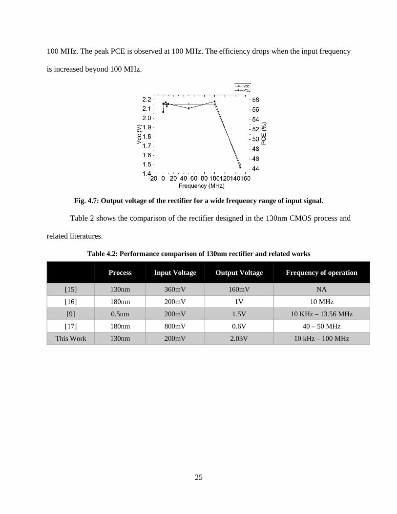
Fig. 4.7 shows the output DC voltage of the rectifier varying from 10 kHz to 150 MHz
frequency range for an input voltage of 200 mV. The output voltage is almost constant (2 V) up to
25
100 MHz. The peak PCE is observed at 100 MHz. The efficiency drops when the input frequency
is increased beyond 100 MHz.
Fig. 4.7: Output voltage of the rectifier for a wide frequency range of input signal.
Table 2 shows the comparison of the rectifier designed in the 130nm CMOS process and
related literatures.
Table 4.2: Performance comparison of 130nm rectifier and related works
Process Input Voltage Output Voltage Frequency of operation
[15] 130nm 360mV 160mV NA
[16] 180nm 200mV 1V 10 MHz
[9] 0.5um 200mV 1.5V 10 KHz – 13.56 MHz
[17] 180nm 800mV 0.6V 40 – 50 MHz
This Work 130nm 200mV 2.03V 10 kHz – 100 MHz

26
CHAPTER 5
CONCLUSION AND FUTURE WORKS
High performance rectifiers for biomedical implant applications have been discussed in
this thesis. The design challenges identified for low-power applications are
• The efficiency.
• The output voltage yield.
• The minimum input voltage the rectifier can convert.
• The operating frequency ranges.
The problem with MOS rectifiers is they cannot rectify AC signals with voltages lower than
200mV. Schottky diodes have been identified to have low threshold voltage, hence consume less
power compared to MOSFETs.
The multi-stage NMOS full-wave rectifier has been modified by replacing the transistors
with Schottky diodes. The circuit has been simulated in the 0.5µm CMOS process and the 130nm
CMOS process. The simulation results show that the design performs better than the architectures
using MOS transistors. The design achieved a maximum efficiency of 89% for 1V at 7.25MHz in
the 0.5µm CMOS process and a maximum efficiency of 59% for 1V at 1MHz in the 130nm CMOS
process. The sizing limitation of the diode in 130nm CMOS process led to a lower efficiency of
the rectifier compared to the 0.5 µm CMOS process. The proposed design works for voltages lower
than 200mV and also works in a wider range of frequencies compared to other architectures using
MOS transistors.
The design can be further improved by using a DC-DC converter after the rectifier. In a
real-case scenario, the input voltage fluctuates a few mV and hence the output voltage keeps

27
varying. This affects the voltage being supplied to the load. A DC-DC converter allows the circuit
to supply a constant voltage to the load, thereby making the system more reliable.

28
REFERENCES
[1] Lu, Y., Li, X., Ki, W. H., Tsui, C. Y., & Yue, C. P. (2013, February). A 13.56 MHz fully integrated 1X/2X active rectifier with compensated bias current for inductively powered devices. In Solid-State Circuits Conference Digest of Technical Papers (ISSCC), 2013 IEEE International (pp. 66-67). IEEE.
[2] Bai, Xiaoyin, Zhi-Hui Kong, and Liter Siek. "A high-efficiency 6.78-MHz full active rectifier with adaptive time delay control for wireless power transmission." IEEE Transactions on Very Large Scale Integration (VLSI) Systems 25.4 (2017): 1297-1306.
[3] Park, Hyung-Gu, et al. "A design of a wireless power receiving unit with a high-efficiency 6.78-MHz active rectifier using shared DLLs for magnetic-resonant A4 WP applications." IEEE Transactions on Power Electronics 31.6 (2016): 4484-4498.
[4] Moh, Kyung-Goo, et al. "12.9 A fully integrated 6W wireless power receiver operating at 6.78 MHz with magnetic resonance coupling." Solid-State Circuits Conference-(ISSCC), 2015 IEEE International. IEEE, 2015.
[5] Ahire, D. B., and Vitthal J. Gond. "Wireless power transfer system for biomedical application: A review." Trends in Electronics and Informatics (ICEI), 2017 International Conference on. IEEE, 2017.
[6] Balanis, Constantine A. "Antenna theory: A review." Proceedings of the IEEE 80.1 (1992): 7-23.
[7] Mazzilli, Francesco, et al. "Design methodology and comparison of rectifiers for UHF-band RFIDs." Radio Frequency Integrated Circuits Symposium (RFIC), 2010 IEEE. IEEE, 2010.
[8] Yi, Jun, Wing-Hung Ki, and Chi-Ying Tsui. "Analysis and design strategy of UHF micro-power CMOS rectifiers for micro-sensor and RFID applications." IEEE Transactions on Circuits and Systems I: Regular Papers 54.1 (2007): 153-166.
[9] Tasneem, N. T., Suri, S. R., & Mahbub, F. (2018, April). A low-power CMOS voltage boosting rectifier for wireless power transfer applications. In 2018 Texas Symposium on Wireless and Microwave Circuits and Systems (WMCS) (pp. 1-4). IEEE.
[10] Liu, J., Chan, K. W., Chung, C. Y., Chan, N. H. L., Liu, M., & Xu, W. (2018). Single-Stage Wireless-Power-Transfer Resonant Converter With Boost Bridgeless Power-Factor-Correction Rectifier. IEEE Transactions on Industrial Electronics, 65(3), 2145-2155.
[11] Musavi, Fariborz, Wilson Eberle, and William G. Dunford. "A high-performance single-phase bridgeless interleaved PFC converter for plug-in hybrid electric vehicle battery chargers." IEEE Transactions on Industry Applications 47.4 (2011): 1833-1843.

29
[12] Stoopman, M., Keyrouz, S., Visser, H. J., Philips, K., & Serdijn, W. A. (2013, June). A self-calibrating RF energy harvester generating 1V at− 26.3 dBm. In VLSI Circuits (VLSIC), 2013 Symposium on (pp. C226-C227). IEEE.
[13] Gougheri, Hesam Sadeghi, and Mehdi Kiani. "Self-regulated reconfigurable voltage/current-mode inductive power management." IEEE Journal of Solid-State Circuits 52.11 (2017): 3056-3070.
[14] Karthaus, Udo, and Martin Fischer. "Fully integrated passive UHF RFID transponder IC with 16.7-µW minimum RF input power." IEEE Journal of Solid-State Circuits 38.10 (2003): 1602-1608.
[15] Zargham, Meysam, and P. Glenn Gulak. "Maximum achievable efficiency in near-field coupled power-transfer systems." IEEE Transactions on Biomedical Circuits and Systems 6.3 (2012): 228-245.
[16] Zargham, Meysam, and P. Glenn Gulak. "High-efficiency CMOS rectifier for fully integrated mW wireless power transfer." Circuits and Systems (ISCAS), 2012 IEEE International Symposium on. IEEE, 2012.
[17] Khan, Mohd Tauheed, Munna Khan, and Mohd Hasan. "High frequency low voltage 32nm node CMOS rectifier for energy harvesting in implantable devices." India Conference (INDICON), 2015 Annual IEEE. IEEE, 2015.
[18] Asmeida, Akrem, et al. "Fast switching wideband rectifying circuit for future RF energy harvesting." AIP Conference Proceedings. Vol. 1883. No. 1. AIP Publishing, 2017.
[19] Rivera, Ben, R. Jacob Baker, and John Melngailis. "Design and layout of Schottky diodes in a standard CMOS process." 2001 International Semiconductor Device Research Symposium, Washington DC. 2001.
[20] Van Zeghbroeck, Bart. "Principles of semiconductor devices." Colarado University 34 (2004).
[21] Cheung, S. K., and N. W. Cheung. "Extraction of Schottky diode parameters from forward current‐voltage characteristics." Applied Physics Letters 49.2 (1986): 85-87.