design of stage-selective negative voltage generator to
TRANSCRIPT

4122 IEEE TRANSACTIONS ON CIRCUITS AND SYSTEMS–I: REGULAR PAPERS, VOL. 67, NO. 11, NOVEMBER 2020
Design of Stage-Selective Negative VoltageGenerator to Improve On-Chip Power Conversion
Efficiency for Neuron StimulationShiau-Pin Lin and Ming-Dou Ker , Fellow, IEEE
Abstract— Dedicated to neuron stimulation circuits, a stage-selective negative voltage generator is proposed to enhance theoverall power efficiency. Since the supplied voltage of the stimulusdriver is subject to applications and treatments, an extensive out-put requirement of supply is demanded to achieve energy-efficientstimulation. The charge pump is implemented as a negative volt-age generator for on-chip design. In a limited area, excess powerloss is eliminated by reconfiguring the cascaded architecture andclocks. Digitally programmable voltage levels can be outputted byvarying the number of stages dynamically. The function of stageselection is achieved by the proposed stage-selective scheme. Withappreciate control, the stage-selective negative voltage generatorcan maintain higher power efficiency under different outputvoltage levels and loading conditions. The technique improves40% power conversion ratio at most but only leads to anincrement of 8% in area occupation. The measured outputvoltage covers from –0.3 V to –9.3 V within a maximum 5.5-mAoutput current, which is verified in a 0.25-µm BCD process.
Index Terms— Stage-selective circuit, stage control, negativevoltage generator, negative charge pump, energy-efficient.
I. INTRODUCTION
AMONG all the DC-to-DC converters, switching capaci-tive converters (i.e. charge pump) are suitable for high-
voltage generation in many applications, especially in neuronstimulation [1]–[8]. Microelectronics-based stimulators delivervoltage or current pulses as electrical stimulation treatmentand treat neurological disorders as well [9]. For the purposesof biomedical stimulation circuits, providing a high voltageto drive a stimulator is the principal objective of a high-voltage generator. Hence, area cost and energy efficiency arethe two major issues to be discussed [10]. Compared withtraditional inductor-based or transformer-based converters, thecharge pump favors the significantly on-chip considerations
Manuscript received March 7, 2020; revised July 20, 2020; acceptedJuly 22, 2020. Date of publication August 4, 2020; date of current versionOctober 30, 2020. This work was supported in part by the Ministry ofEducation (MOE) through the SPROUT Project, Center for NeuromodulationMedical Electronics Systems of National Chiao-Tung University, Taiwan, inpart by the Ministry of Science and Technology (MOST), Taiwan underContract MOST 108-2321-B-009-007-MY2, and in part by the fabricationof silicon chip through the Taiwan Semiconductor Research Institute (TSRI).This article was recommended by Associate Editor F. M. Neri. (Correspondingauthor: Ming-Dou Ker.)
The authors are with the Biomedical Electronics Translational ResearchCenter, National Chiao-Tung University, Hsinchu 300, Taiwan (e-mail:[email protected]).
Color versions of one or more of the figures in this article are availableonline at http://ieeexplore.ieee.org.
Digital Object Identifier 10.1109/TCSI.2020.3012086
Fig. 1. A conceptual stimulation system for energy conservation includesthe variable supply, the detecting circuit, and the stimulator. In this paper,a new proposal of the variable supply is composed of a stage controller andnegative charge pump.
on area concerns. From the perspective of energy efficiency,it is strongly related to battery lifetime for a long period ofusage. Without any off-chip components, the charge pump caneffectively generate positive or negative high voltage from alower voltage by different charge pump topologies. Therefore,it can support stimulators to deliver desired stimulus patterns.However, the organic impedance may be varied or the stimulusscale may be changed during therapeutic processes. It indicatesthat the required supply for stimulators is not always a fixedvalue [5]–[7]. In fact, it varies from several volts to tensof volts [8]. To make stimulators work more conservative,a charge pump with a wide output range is developed.
In a stimulation system, a variable supply system is anadvanced integration to provide expected power dynamicallyand efficiently. A conceptual system is drawn in Fig. 1,containing a variable supply system, a detecting system, andstimulus drivers. In order to maximize the overall efficiencyof implantable stimulators, adaptive power supply techniquesare required to minimize the voltage drop across the stimuligenerator. Some algorithms are imperative as criteria fordynamic reconfigurability. One of the detection circuits isaccomplished by the electrode monitoring circuit (EMC) [6].It can immediately measure the electrode output voltage andfurther tell the sufficiency of power supply by comparing theoutput voltage of electrodes and the high voltage generator.A stimulator buffer with a triode indicator [7] is used to
1549-8328 © 2020 IEEE. Personal use is permitted, but republication/redistribution requires IEEE permission.See https://www.ieee.org/publications/rights/index.html for more information.
Authorized licensed use limited to: National Chiao Tung Univ.. Downloaded on November 02,2020 at 10:21:11 UTC from IEEE Xplore. Restrictions apply.
LIN AND KER: DESIGN OF STAGE-SELECTIVE NEGATIVE VOLTAGE GENERATOR 4123
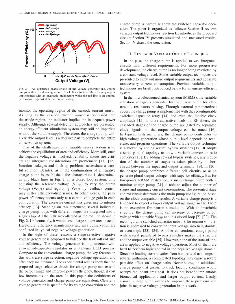
Fig. 2. An illustrated characteristic of the voltage generator (i.e. chargepump) with a fixed configuration. Black lines indicate the charge pump isimplemented with an invariable architecture while the red line is an optimalperformance against different output voltage.
monitor the operating region of the cascode current mirror.As long as the cascode current mirror is oppressed intothe triode region, the indicator implies the inadequate powersupply. Although several detection approaches are presented,an energy-efficient stimulation system may still be imperfectwithout the variable supply. Therefore, the charge pump witha variable output level is a decisive part to complete the entireconservative system.
One of the challenges of a variable supply system is toachieve the equilibrium of area and efficiency. More still, oncethe negative voltage is involved, reliability issues are criti-cal and integrated considerations are problematic [11], [12].Junction leakages and latch-up problems necessitate a care-ful solution. Besides, as if the configuration of a negativecharge pump is established, the characteristic is determinedas any black lines in Fig. 2. In a closed-loop system, onlyadjusting the reference voltage (VREF) to vary the outputvoltage (VOUT) and regulating VOUT by feedback controlmay suffer efficiency-drop issues. In other words, the peakpower efficiency occurs only at a certain voltage gain in eachconfiguration. The excessive current loss gives rise to inferiorefficacy [13]. Standing on this statement, several individualcharge pump loops with different stages are integrated into asingle chip. All the hills are collected as the red line shown inFig. 2. Unfortunately, it would cost a large silicon area instead.Heretofore, efficiency maintenance and area conservation areconflicted in typical negative voltage generation.
In the sight of these reasons, a stage-selective negativevoltage generator is proposed to balance the trade-offs of sizeand efficiency. The voltage generator is implemented witha switched-capacitor regulator in a 0.25-μm BCD process.Compare to the conventional charge pump, the key features inthis work are stage selection, negative voltage operation, andefficiency maintenance. The experimental results show that theproposed stage-selective circuit for charge pump can extendthe output range and improve power efficiency, though it costfew increments on the area. In this paper, the definitions ofvoltage generator and charge pump are equivalent. Clearly, avoltage generator is specific for its voltage conversion and the
charge pump is particular about the switched capacitor oper-ation. The paper is organized as follows: Section II reviewsvariable output techniques; Section III introduces the proposedcircuit; Section IV presents simulated and measured results;Section V draws the conclusion.
II. REVIEW OF VARIABLE OUTPUT TECHNIQUES
In the past, the charge pump is applied to vast integratedcircuits with different requirements. For more progressivedevelopment, the charge pump is no longer being restricted bya constant voltage level. Some variable output techniques arepresented to carry out more output requirements and conserveunnecessary current consumption. Previous variable outputtechniques are briefly introduced below for an energy-efficientsystem.
In the microelectromechanical system (MEMS), the variableactuation voltage is generated by the charge pump for elec-trostatic resonators biasing. Through external parameterizedcodes, the charge pump is implemented with the reconfigurableswitched capacitor array [14] and even the tunable clockamplitude [15] to drive capacitive loads. In RF filters, thecascaded stages of the charge pump are gated by separatedclock signals, so the output voltage can be tuned [16].In typical flash memories, the charge pump contributes tohigh voltage generation whose output level depends on read,erase, and program operations. The variable output techniqueis achieved by adding several bypass switches [17]. It adoptsa serial-parallel topology to draw a variable-conversion-ratioconverter [18]. By adding several bypass switches, any reduc-tion of the number of stages is taken place by a shortcircuit between the input and output terminals [19]. In [20],the charge pump combines different cell circuits so as togenerate plural output voltages with superior efficacy. But forlow-power RRAM realization, a main charge pump with amonitor charge pump [21] is able to adjust the number ofstages and minimize current consumption. The presented stagecontrol circuit determines the main pump configuration basedon the clock comparison results. A variable charge pump is atendency to export a larger output voltage range so far. Thereis no exception for neuron stimulation. With an invariablestructure, the charge pump can increase or decrease outputvoltage with a tunable VREF and in a closed-loop [7], [22]. Thereconfigurable switched-capacitor network for neuron stimula-tion is addressed to convert an input voltage into half, double,or even triple [23], [24]. Another conventional charge pumpwith several paralleled bypass switches makes the structureand the output variable [25]. However, none of the state-of-the-art is applied to negative voltage operation. Most of them arehard to perform logic control in the negative voltage domain.Since the loading current varies from hundreds of nanoamps toseveral milliamps, a complicated topology may cause a severeparasitic effect on charge paths. Nevertheless, an additionalcharge pump that assists to track loading conditions wouldoccupy redundant area cost. It does not benefit implantablebiomedical applications and larger output current. Lastly,a novel charge pump intends to improve these problems andjoins in negative voltage generation in this work.
Authorized licensed use limited to: National Chiao Tung Univ.. Downloaded on November 02,2020 at 10:21:11 UTC from IEEE Xplore. Restrictions apply.

4124 IEEE TRANSACTIONS ON CIRCUITS AND SYSTEMS–I: REGULAR PAPERS, VOL. 67, NO. 11, NOVEMBER 2020
III. PROPOSED STAGE-SELECTIVE NEGATIVE
VOLTAGE GENERATOR
A stage-selective negative voltage generator is proposed toenhance the overall power efficiency within a limited area.Typically, power losses can be classified as conduction loss,switching loss, redistribution loss and reversion loss [26].A switched-capacitor converter performs better efficiencythrough proper optimization among a variety of power losses.For a wide output range, efficiency decay appears at low volt-age gain cases. Power dissipates through charge conductionloss and switching loss is worsening due to more charge pumpstages cascaded. Redistribution loss takes place at chargesharing between any two capacitors. The last reversion loss isabout an undesirable short circuit path in the power stage ofthe negative charge pump. In this work, the main concept is togenerate the desired output voltage with appropriate activatedstages and eliminate excess power loss.
A. Proposed Stage-Selective Circuit
In a conventional configuration of the negative charge pump,charge pump cells are cascaded stage by stage and fixed.A proposed stage-selective circuit is added to make the config-uration more flexible. In this work, there are two operationalmodes: pump mode and bypass mode. The “pump mode” isdefined to increase the activated stage number of negativecharge pump whereas the “bypass mode” is to decrease theactivated stage number. In other words, the charge transferpath would be reconfigured from N to more than N stages inthe pump mode, but it would be reconfigured from N to lessthan N stages in the bypass mode, where N represents thenumber of the activated charge pump cells.
As shown in Fig. 3(a), the operational mode is specifiedby the digital signals SN and CN through the correspondingcontrollers. In each stage, the stage-selective circuit consistsof a stage controller, a negative level shifter (NLSN), and abypass switch (MN). The external digital signal SN is refinedby the stage controller for time delay and then delivered as aninternal control signal SNIN. Besides, the bias VHN is given bythe stage controller as the power node of the NLS. Once theNLS received SNIN, it would convert and extend the voltagedomain from positive to negative at SNOUT and SWN. In anNLS, MP1 and MP2 are used to sense input voltage levels. Theassociated connection is annotated in Fig. 4. By comparing thepull-up current of PMOS (MP1 and MP2) and the pull-downcurrent of NMOS (MN1 and MN2), the output signals SWN ofnegative level shifters are requested to either fully conductedor completely cut off the bypass switches (MN). When SWNis connected to VHN which is a positive potential (equal toVDDH), MN would be fully turned on. Charges transfer throughthe bypass switch (MN). When SWN is tied to VLN which is anegative potential, MN would be turned off. Moreover, a clockcontroller is commanded by the digital signal CN. CN controlswhether the clock signal of the whole system is able to deliverinto the charge pump cell or not. When the charge pump stageis bypassed by the SN signal, the clock controller disconnectsthe clock to save some energy by CN signal. To be brief, SN
determines the operating mode of the selected Nth stage alongwith CN whether to pump up or bypass away VLN.
B. Operative Mechanism
Because of the similar composition in each stage, theoperation is introduced in Fig. 3(b) and Fig. 3(c). In orderto pump up the voltage in Fig. 3(b), the stage control signal(SN) would go low to turn off the bypass path. Then, the clockcontrol signal (CN) would go high to pass the clock signalinto the core circuit. Thus, the output voltage at VLN can bepumped to a more negative value with the system frequency.The charge path is diverted from the Nth bypass switch intothe negative charge pump cell. In short, a low SN and a highCN declare that the selected Nth stage is operating in the pumpmode. On the contrary, SN would be pulled high when enteringthe bypass mode as shown in Fig. 3(c). A high SN conductsthe selected bypass switch and makes the excessive voltage atVLN bypassed away. Meanwhile, CN would be pulled low toshut off the corresponding clock controller, and further stop theclock toggling in the Nth four-phase clock generator. Hence,the core charge pump circuit is ceased and no longer delivercharges. The charge transfer path is substituted by the bypassswitch. A higher value (i.e. less negative) at VLN may beachieved with less energy loss due to the short circuit of MN.
The closed-loop negative voltage generator with the stage-selective is presented in Fig. 5. Since the bypass switch isconnected between the first input terminal (VIN, 0 V) and theNth output terminal (VLN), there is an order to pump or bypassthe charge pump stages from which direction. For pumping,the power stage which is nearer the output terminal has thepriority to be activated (i.e. pump 1st-, 2nd-, 3rd-, and 4th-stagein order). But for bypassing, it begins from the one nearer theinput terminal to disable the power stage (i.e. bypass 4th-, 3rd-,2nd-, and 1st- stage in order). The arrangement makes theproposed scheme not only flexible but also reconfigurable.
A four-stage composition is adopted in Fig. 5. The negativecharge pump cells are successively jointed. The proposedcircuit is replicated and connected to the cells accordingly.Charges are sent from the input terminal (VIN) and storedin the output capacitor (CO1) at the output terminal (VL1).In general, the input voltage at VIN is 0 V as well as theground. For example, the negative voltage generator is setto a four-stage configuration initially. Yet, the composition isexpected to cut down by half for energy conservation. To pre-vent unknown conditions and residual charges, the fourth andthe third power stages are bypassed in sequence. By con-ducting M4 and turning off CLK4, VL4 would be releasedto the input voltage level (VIN, 0 V). And then the sim-ilar progress is repeated in the third stage. A fully conductedM3 gives the input 0 V to VL3. Clock signals are no longercoupled into the charge pump cell thanks to an open CLK3.VL3 is discharged gradually as well as VL1. Lastly, only thesecond and the first stages are available so that charges aredelivered to VL1 with a two-stage configuration of the negativevoltage generator. The charge transfer path is changed frompath A to path B and finally path C, as annotated in Fig. 5.Somehow a lower output voltage (more negative) is needed
Authorized licensed use limited to: National Chiao Tung Univ.. Downloaded on November 02,2020 at 10:21:11 UTC from IEEE Xplore. Restrictions apply.

LIN AND KER: DESIGN OF STAGE-SELECTIVE NEGATIVE VOLTAGE GENERATOR 4125
Fig. 3. (a) The unit structure of the proposed stage-selective circuit in the Nth stage. The operation of each selected stage with corresponding control signals.(b) In the pump mode, SN is low but CN is high; thus, the Nth-stage negative charge pump becomes the primary charge transfer path. (c) In the bypass mode,SN turns high and CN turns low so that charges directly pass through the Nth-stage bypass switch (MN).
Fig. 4. The detailed circuit schematic of the negative level shifter (NLS).
at VL1. Therefore, the negative voltage generator returns to thefour-stage configuration by means of enabling the third and thefourth stages. To boost a more negative voltage, it is necessaryto cut off the bypass path, which is created by M3 and M4. Theentire closed-loop system would attempt to regulate VL1 bytoggling clock signals. In this event, CLK3 and CLK4 are shortto transfer clocks into four-phase clock generators. A morenegative output voltage is produced at VL1 in the end. Thecharge transfer path is changed from path C to path B andfinally path A, as annotated in Fig. 5.
When the loop is locked at a certain output level, morethan one configuration might be able to achieve this scenario.If excessive power stages and clock generators are activatedto meet the specification, too many charges would be redis-tributed. And further, more energy is dissipated. In contrast,the lack of activated stages and clock generators may induceoverclocking, thereby the more switching loss getting worse.Thus, a competent configuration can perform better efficiencyand stability with exact power stages and clocks. Depending
on the conversion ratio, the power loss of the pumping stagecan be optimized by the proposed circuit. The output voltageat VL1 can provide the desired value with less power loss.
C. Circuit Implementation
In Fig. 5, the affiliated circuits comprise the voltage divider,the reference bias circuit, the error amplifier, the voltagecontrol oscillator (VCO), positive level shifters, the four-phaseclock generator, and the four-stage charge pump. For moredetails, a resistive digital-to-analog converter (RDAC) is areference bias circuit in binary-weighted R-2R networks. Thegenerated voltage (VREF) of RDAC is controlled by five-bitsignals R[1:5]. According to the reference voltage (VREF) andthe resistive divider, the output of the charge pump loop wouldbe locked at a target voltage level (VTG). Whether the cascadedconfiguration or the output current is, the proposed stage -selective negative charge pump is seen as a self-regulatedclosed-loop unit with pulse frequency modulation (PFM) feed-back control. It is notable that the error amplifier is designedwith a wide bandwidth to trace the desired output target.Considered to a quick start-up and numerous output loadingconditions, the oscillation frequency of the VCO should coverfrom several MHz to tens of MHz. In addition, a four-phasecross-couple structure is adopted as the core circuit of thenegative charge pump cell [27]. The specific connection andthe four-phase sequence of the charge pump cell are presentedin Fig. 6. This topology is free from overstress issues becauseonly 1×VDDH is delivered in each cascaded stage. For the rea-son that the power domain of the four-phase clock generator isVDDH, the clock edges would only couple the toggling signals
Authorized licensed use limited to: National Chiao Tung Univ.. Downloaded on November 02,2020 at 10:21:11 UTC from IEEE Xplore. Restrictions apply.

4126 IEEE TRANSACTIONS ON CIRCUITS AND SYSTEMS–I: REGULAR PAPERS, VOL. 67, NO. 11, NOVEMBER 2020
Fig. 5. The block diagram of the proposed stage-selective negative voltage generator.
Fig. 6. (a) The circuit schematic and (b) the corresponding four-phaseclocking waveforms of the negative charge pump cell.
with 1×VDDH. Overstress concerns in charge pump cells areeliminated. The four-phase operation releases the return-backleakage and reversion loss. By virtue of the biomedical SoCintegration, the global P-substrate is tied to 0 V as a ground.
Fig. 7. The cross-section view of (a) PMOS forbidden to implement in thenegative voltage domain and (b) NMOS with an isolated ring used in thenegative charge pump cell.
For the sake of operation in the negative voltage, PMOSis forbidden to implement in all negative voltage domains,unless high voltage devices. Otherwise, PMOS could resultin the forward parasitic diode in Fig.7 (a). All the switchesare implemented in NMOS with isolation. The isolated ring isprovided in the process with a deep P-well and a N+ buriedlayer (NBL) ring. The source and bulk terminals are jointedto avoid body effect. All NMOS are immersed in negativevoltage, and the bias potential of P-well bulk ring and deepP-well ring is also negative. But the NBL is biased at VDDHwhich is the highest voltage in the entire system. All theparasitic PN-junctions are reverse biased to prevent junctionleakage. In Fig. 7(b), it annotates the practical bias conditionsand the cross-section view of a switch in one charge pumpcell.
IV. VERIFICATIONS AND DISCUSSIONS
The proposed negative voltage generator with stage- selec-tive circuits verifies the design on area and efficiency main-tenance. Furthermore, configuration diversity is improved byadditional bypass switches. This work has been fabricated in a
Authorized licensed use limited to: National Chiao Tung Univ.. Downloaded on November 02,2020 at 10:21:11 UTC from IEEE Xplore. Restrictions apply.

LIN AND KER: DESIGN OF STAGE-SELECTIVE NEGATIVE VOLTAGE GENERATOR 4127
Fig. 8. The simulated results of the negative voltage generator to demonstrateits start-up and regulation.
TSMC 0.25-μm 2.5-V/5-V/12-V BCD process. In this process,the thick oxide in 12-V devices can tolerate the high voltagestress, yet the threshold voltage is high. Therefore, they areonly adopted to NLSN and MN in the proposed stage-selectivecircuit. The maximum voltage difference in NLSN and MN isabout 13 V in this work.
A. Simulation and Comparisons
For implantable biomedical applications, the impedanceof electrodes and tissue varies with the size and position ofthe electrode. In neuron stimulation, the impedance value ofthe human brain is about 1 k� to 3 k�. The requisitionof the power supply of stimulus drivers is widespread foreither constant voltage or constant current stimulation. Thus,the stage- selective negative voltage generator is designed tooutput a wide voltage range within 5.5-mA output current. Theoutput voltage (VL1) is expected to regulate from –0.3 V to–9.3 V with the supplied voltages of 1.8 V (VDDL) and 3 V(VDDH). In this work, VDDL is for analog circuits to minimizepower. Yet VDDH is for clock generators to couple the pumpingcapacitors. Aforementioned above, the analog type VCO givesaround 100 MHz clocks to boost VL1, so the quick start-uptakes only 1 μs to reach the target voltage in Fig. 8. As longas the voltage is achieved, the clock frequency would slowdown but still keep toggling to regulate by the PFM control.
Since the negative charge pump is implemented with fourstages, the charge path can be reconfigured as zero-stage,one-stage, two-stage, three-stage, and four-stage in total. Thezero-stage is for discharging and reset. Each configuration isborn with its characteristic curves on power efficiency andoutput voltage. The simulated results under different loadingconditions were explained in Fig. 9 (solid), including theminimum 0.5-mA and maximum 5.5-mA output current. Themaximum voltage conversion is to couple 1×VDDH in eachstage. When the voltage conversion ratio is between 60% and80%, power losses are optimized to make the overall efficacybetter. In other words, if the activated stages are appropriatefor the output voltage levels, the power efficiency would bekept at a higher performance.
Fig. 9. The simulated and measured characteristics of the stage-selectivenegative voltage generator. (a) Under 0.5-mA output current (light load).(b) Under 5.5-mA output current (heavy load).
When the target level is loose, the major power loss isattributed to redistribution loss. Some of the delivered energyis dropped out so that the power efficiency is lower. However,when the target level is tight, the entire negative voltagegenerator is operated under a higher frequency. The powerefficiency would drop dramatically as a result of the massiveswitching loss. Therefore, only a particular zone is preservedto achieve the expected efficiency without reconfigurablepumping schemes. Collecting the peak power efficiency ofeach configuration, the characteristic curves of this work arefeatured with the four successive hills. With stage selection,the simulated power efficiency is around 35% to 40% at valleysand roughly 50% at hilltops. As a result, the proposed negativevoltage generator holds a better configuration and keeps ahigher efficiency.
B. Silicon Verifications
The die microphotograph of the stage-selective negativevoltage generator chip is shown in Fig. 10. Excluding I/O pads,the test chip occupies a silicon area of 2.25 mm2. To furtherbreak down, 8% is occupied by the proposed stage-selection
Authorized licensed use limited to: National Chiao Tung Univ.. Downloaded on November 02,2020 at 10:21:11 UTC from IEEE Xplore. Restrictions apply.

4128 IEEE TRANSACTIONS ON CIRCUITS AND SYSTEMS–I: REGULAR PAPERS, VOL. 67, NO. 11, NOVEMBER 2020
Fig. 10. Die microphotograph of the fabricated stage-selective negativevoltage generator.
circuits, 87% is the power stages and all on-chip capacitors,and the rest 5% is the peripheral PFM circuits. For on-chiprealization, all the capacitors are implemented with the metal-insulator-metal (MIM) capacitors. According to different pur-poses, capacitors are sorted into pumping capacitors (CP),auxiliary capacitors (Caux), and output capacitors (COUT). CPis a fly capacitor of 100 pF so as to couple 1×VDDH. Cauxwhich is sized to 2.5 pF only helps the main transistors forconduction. In addition, COUT at the output node (VL1) isdrawn with 125 pF to store charges and reduce output ripples.
As mentioned above, each configuration possesses its owncharacteristic curves on power efficiency and output voltage.The silicon measured results are presented in Fig. 11. Whenthe configuration is fixed to certain stages, it can only varyoutput levels by adjusting VREF and suffer low efficiency atless negative voltage cases. The major object is to combinethose high efficiency parts in each configuration, and the foursuccessive hills are gathered in Fig. 9 (hollow). The proposedcircuit is verified to enhance the power conversion ratio around40% to 55% with the assistant of the stage-selective circuitin measurements. Owing to the complex control sequence,digital codes are programmed into an external testing boardand delivered to the internal test chip. Several control signalsmake the proposed negative voltage generator more flexible.The architecture is not fixed and the output is not constant,either. In this work, stage control signals (S[1:4]) and clockcontrol signals (C[1:4]) are given to reconfigure the cascadedstructure and clocks. In each configuration, reference controlsignals (R[1:5]) further alter the regulated target voltage. Exceptthe Enable signal is still manually controlled, other controlsignals come from digital control. As shown in Fig. 12(a),the fabricated chip is requested to alter VL1 from –0.3 Vto –9.3 V. The output impedance is 2 k�. In contrast, VL1in Fig. 12(b) is initially pumped to a negative high leveland then stepped down. In a closed-loop system, the PFMfeedback control technique is applied to regulate VL1 atnumerous levels. Under the optimized and activated stages,VL1 is set with a resolution of –0.5 V. Whether it is operatedin pump mode (Fig. 12(a)) or in bypass mode (Fig. 12(b)),the proposed circuit succeeds to expand the output voltagerange and improves the low-efficiency issue. The variable
Fig. 11. The measured characteristics of the negative voltage generator withdifferent cascaded configuration. (a) Under 0.5-mA output current (light load).(b) Under 5.5-mA output current (heavy load).
technique is mainly for energy-efficient motivation, and theslight voltage shift avoids spikes from damages. Since VL1usually supports stimulators in biomedical SoC, increasing thesupply of stimulators step by step performs a soft start-up.Decreasing the supply is to discharge and reset for thoroughpower-off. In Fig. 12 (c), the proposed stage-selective circuitis operated in order so that the configuration is transformedstage by stage. Under corresponding activated stages, VL1 islocked at different objects. For instance, VL1 is stabilized at–1.8 V with one stage validated, –3.3 V with two stages, –5.8 V with three stages, and –8.3 V with four stages. Themeasured results are recorded on waveforms. Moreover, it canalso change the entire cascaded architecture arbitrarily. Despitethe irregular transformation, the whole system is still able tosettle on the target voltage. As depicted in Fig. 12(d), theconfiguration is varied out of order. Focusing on the transientstate, VL1 is able to regulate at a certain target voltage with thefeedback control. The negative voltage generator is composedof a four-stage configuration, as a result, a stable –9.3-Voutput voltage is delivered under a 5.5-mA current loading,as demonstrated in Fig. 13(a). The internal nodes, includingVL2, VL3, and VL4, are also presented to explain the voltage
Authorized licensed use limited to: National Chiao Tung Univ.. Downloaded on November 02,2020 at 10:21:11 UTC from IEEE Xplore. Restrictions apply.

LIN AND KER: DESIGN OF STAGE-SELECTIVE NEGATIVE VOLTAGE GENERATOR 4129
Fig. 12. The measured results of the stage-selective negative voltage generator operated (a) in the pump mode and (b) in the bypass mode. For special cases,the reference values and the activated stages of the stage-selective negative voltage generator are varied (c) in order and (d) out of order. All the measuredevents are verified with the output impedance of 2-k� (heavy load).
Fig. 13. (a) The measured results of the stage-selective negative voltage generator at –9.3-V output voltage and 5.5-mA loading current by a four-stageconfiguration. (b) The measured results of the stage-selective negative voltage generator at –4.3-V output voltage and 3.5-mA loading current by a two-stageconfiguration.
conversion ratio in each stage. In addition, it can also providea –4.3-V output voltage and a 3.5-mA current loading with atwo-stage configuration in Fig. 13(b). Since the third and thefourth stages are bypassed, VL4 and VL3 are short to the inputterminal as well as 0 V. Under different loading conditions,the functions and performances are verified in silicon chips.
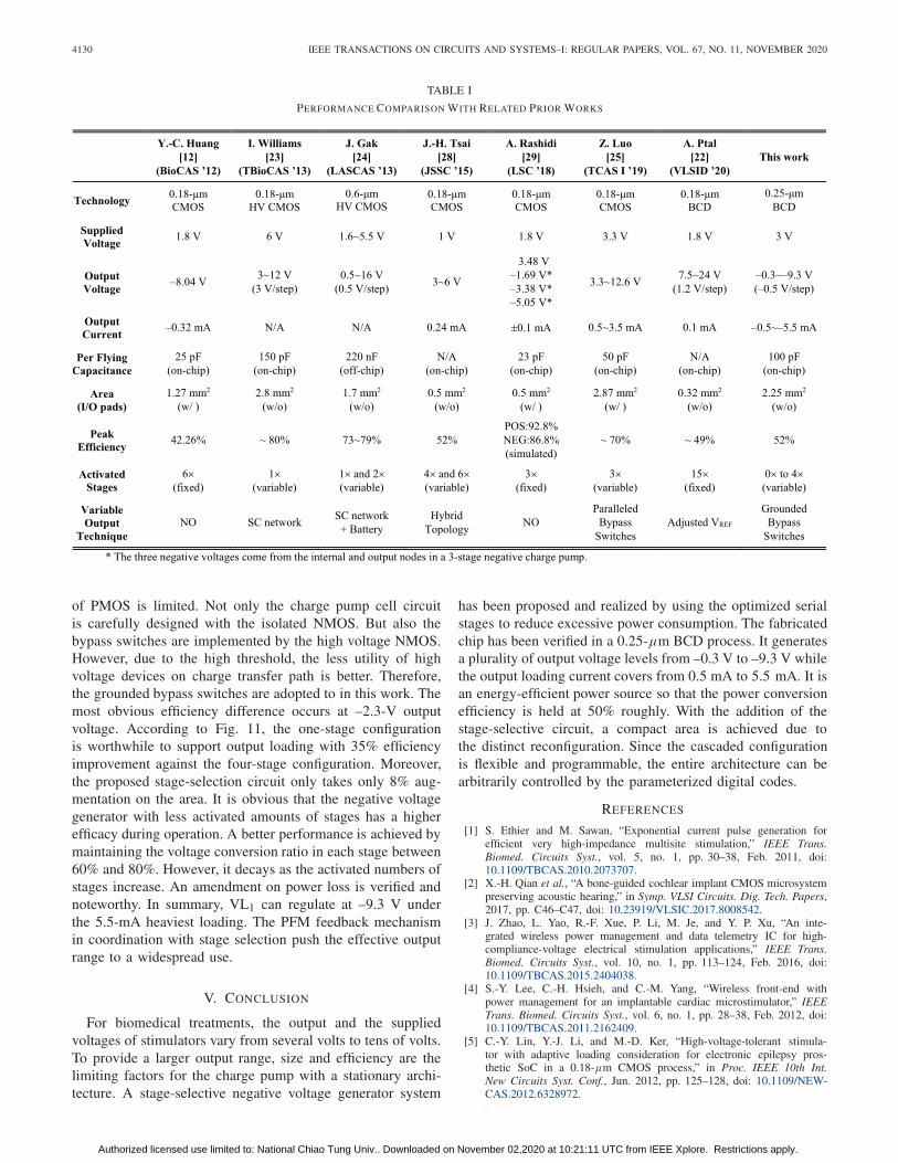
Based on these measured results, specifications of thefabricated stage-selective negative voltage generator are sum-marized in Table I and compared to other previous works.On the basis of negative voltage, this work takes advantageof a wide output voltage range and a large output currentloading. With stage selection, an extensive voltage range andefficient power conversion have been accomplished and veri-fied. The entire performance is flexible rather than fixed outputor fixed charge transfer scheme. The new proposal of thevariable output scheme can be realized in the negative voltage.
From the perspective of a reconfigurable negative voltage gen-erator, the overall power efficiency is optimized and enhanced.The proposed stage-selection circuit profits from making aproper voltage conversion for each power stage.
C. Discussion
Since input current is consumed consistent with activatedpumping stages and clocks, it is important to dispose ofredundant pumping blocks. In other words, it may easilysuffer low-efficiency issues without stage selection when theactivated stages and clocks are not fit for the output voltagelevels. On the contrary, stage selection is able to maintainhigher power efficiency under different output voltage lev-els. The greatest originality in this work is to realize thestage-selective circuit in the negative voltage domain. SinceP-substrate is connected to 0 V for integration, the usage
Authorized licensed use limited to: National Chiao Tung Univ.. Downloaded on November 02,2020 at 10:21:11 UTC from IEEE Xplore. Restrictions apply.
4130 IEEE TRANSACTIONS ON CIRCUITS AND SYSTEMS–I: REGULAR PAPERS, VOL. 67, NO. 11, NOVEMBER 2020
TABLE I
PERFORMANCE COMPARISON WITH RELATED PRIOR WORKS
of PMOS is limited. Not only the charge pump cell circuitis carefully designed with the isolated NMOS. But also thebypass switches are implemented by the high voltage NMOS.However, due to the high threshold, the less utility of highvoltage devices on charge transfer path is better. Therefore,the grounded bypass switches are adopted to in this work. Themost obvious efficiency difference occurs at –2.3-V outputvoltage. According to Fig. 11, the one-stage configurationis worthwhile to support output loading with 35% efficiencyimprovement against the four-stage configuration. Moreover,the proposed stage-selection circuit only takes only 8% aug-mentation on the area. It is obvious that the negative voltagegenerator with less activated amounts of stages has a higherefficacy during operation. A better performance is achieved bymaintaining the voltage conversion ratio in each stage between60% and 80%. However, it decays as the activated numbers ofstages increase. An amendment on power loss is verified andnoteworthy. In summary, VL1 can regulate at –9.3 V underthe 5.5-mA heaviest loading. The PFM feedback mechanismin coordination with stage selection push the effective outputrange to a widespread use.
V. CONCLUSION
For biomedical treatments, the output and the suppliedvoltages of stimulators vary from several volts to tens of volts.To provide a larger output range, size and efficiency are thelimiting factors for the charge pump with a stationary archi-tecture. A stage-selective negative voltage generator system
has been proposed and realized by using the optimized serialstages to reduce excessive power consumption. The fabricatedchip has been verified in a 0.25-μm BCD process. It generatesa plurality of output voltage levels from –0.3 V to –9.3 V whilethe output loading current covers from 0.5 mA to 5.5 mA. It isan energy-efficient power source so that the power conversionefficiency is held at 50% roughly. With the addition of thestage-selective circuit, a compact area is achieved due tothe distinct reconfiguration. Since the cascaded configurationis flexible and programmable, the entire architecture can bearbitrarily controlled by the parameterized digital codes.
REFERENCES
[1] S. Ethier and M. Sawan, “Exponential current pulse generation forefficient very high-impedance multisite stimulation,” IEEE Trans.Biomed. Circuits Syst., vol. 5, no. 1, pp. 30–38, Feb. 2011, doi:10.1109/TBCAS.2010.2073707.
[2] X.-H. Qian et al., “A bone-guided cochlear implant CMOS microsystempreserving acoustic hearing,” in Symp. VLSI Circuits. Dig. Tech. Papers,2017, pp. C46–C47, doi: 10.23919/VLSIC.2017.8008542.
[3] J. Zhao, L. Yao, R.-F. Xue, P. Li, M. Je, and Y. P. Xu, “An inte-grated wireless power management and data telemetry IC for high-compliance-voltage electrical stimulation applications,” IEEE Trans.Biomed. Circuits Syst., vol. 10, no. 1, pp. 113–124, Feb. 2016, doi:10.1109/TBCAS.2015.2404038.
[4] S.-Y. Lee, C.-H. Hsieh, and C.-M. Yang, “Wireless front-end withpower management for an implantable cardiac microstimulator,” IEEETrans. Biomed. Circuits Syst., vol. 6, no. 1, pp. 28–38, Feb. 2012, doi:10.1109/TBCAS.2011.2162409.
[5] C.-Y. Lin, Y.-J. Li, and M.-D. Ker, “High-voltage-tolerant stimula-tor with adaptive loading consideration for electronic epilepsy pros-thetic SoC in a 0.18-μm CMOS process,” in Proc. IEEE 10th Int.New Circuits Syst. Conf., Jun. 2012, pp. 125–128, doi: 10.1109/NEW-CAS.2012.6328972.
Authorized licensed use limited to: National Chiao Tung Univ.. Downloaded on November 02,2020 at 10:21:11 UTC from IEEE Xplore. Restrictions apply.

LIN AND KER: DESIGN OF STAGE-SELECTIVE NEGATIVE VOLTAGE GENERATOR 4131
[6] E. K. F. Lee, “A 45 V 10-b electrode monitoring analog-to-digitalconverter,” in Proc. IEEE Int. Symp. Circuits Syst. (ISCAS), May 2015,pp. 1238–1241, doi: 10.1109/ISCAS.2015.7168864.
[7] Z. Luo, M.-D. Ker, T.-Y. Yang, and W.-H. Cheng, “A digitally dynamicpower supply technique for 16-channel 12 V-tolerant stimulator realizedin a 0.18-μm 1.8-V/3.3-V low-voltage CMOS process,” IEEE Trans.Biomed. Circuits Syst., vol. 11, no. 5, pp. 1087–1096, Oct. 2017, doi:10.1109/TBCAS.2017.2713122.
[8] M.-D. Ker, C.-Y. Lin, and W.-L. Chen, “Stimulus driver for epilepsyseizure suppression with adaptive loading impedance,” J. NeuralEng., vol. 8, no. 6, Oct. 2011, Art. no. 066008, doi: 10.1088/1741-2560/8/6/066008.
[9] P. H. Peckham and J. S. Knutson, “Functional electrical stimulationfor neuromuscular applications,” Annu. Rev. Biomed. Eng., vol. 7, no. 1,pp. 327–360, Aug. 2005, doi: 10.1146/annurev.bioeng.6.040803.140103.
[10] G. Palumbo and D. Pappalardo, “Charge pump circuits: An overviewon design strategies and topologies,” IEEE Circuits Syst. Mag., vol. 10,no. 1, pp. 31–45, Mar. 2010, doi: 10.1109/MCAS.2009.935695.
[11] S. Ethier, M. Sawan, E. Aboulhamid, and M. El-Gamal, “A ±9 V fullyintegrated CMOS electrode driver for high-impedance microstimula-tion,” in Proc. IEEE 52nd Int. Midwest Symp. Circuits Syst., Aug. 2009,pp. 192–195, doi: 10.1109/MWSCAS.2009.5236121.
[12] Y.-C. Huang, M.-D. Ker, and C.-Y. Lin, “Design of negative high voltagegenerator for biphasic stimulator with SoC integration consideration,”in Proc. IEEE Biomed. Circuits Syst. Conf., Nov. 2012, pp. 29–32, doi:10.1109/BioCAS.2012.6418477.
[13] G. Palumbo, D. Pappalardo, and M. Gaibotti, “Charge-pump circuits:Power-consumption optimization,” IEEE Trans. Circuits Syst. I, Fun-dam. Theory Appl., vol. 49, no. 11, pp. 1535–1542, Nov. 2002, doi:10.1109/TCSI.2002.804544.
[14] K.-J. Choi and D.-W. Jee, “High-efficiency, 6.6–29 V pulse driver usingcharge redistribution,” Electron. Lett., vol. 54, no. 12, pp. 746–748,Jun. 2018, doi: 10.1049/el.2018.0800.
[15] A.-H. Alameh and F. Nabki, “A 0.13-μm CMOS dynamically recon-figurable charge pump for electrostatic MEMS actuation,” IEEE Trans.Very Large Scale Integr. (VLSI) Syst., vol. 25, no. 4, pp. 1261–1270,Apr. 2017, doi: 10.1109/TVLSI.2016.2629439.
[16] M. A. Khater and D. Peroulis, “Variable-output charge-pump forpiezoelectric and electrostatic tunable RF filters,” in Proc. IEEEInt. Symp. Circuits Syst., May 2015, pp. 1362–1365, doi: 10.1109/ISCAS.2015.7168895.
[17] S.-K. Won et al., “High-voltage wordline generator for low-power pro-gram operation in NAND flash memories,” in Proc. IEEE Asian Solid-State Circuits Conf., Nov. 2011, pp. 169–172, doi: 10.1109/ASSCC.2011.6123629.
[18] Y.-H. Chang, “Variable-conversion-ratio switched-capacitor-voltage-multiplier/divider DC–DC converter,” IEEE Trans. Circuits Syst.I, Reg. Papers, vol. 58, no. 8, pp. 1944–1957, Aug. 2011, doi:10.1109/TCSI.2010.2103171.
[19] G. Palumbo, D. Pappalardo, and M. Gaibotti, “Charge pump with adap-tive stages for non-volatile memories,” IEE Proc.-Circuits, Devices Syst.,vol. 153, no. 2, pp. 136–142, Apr. 2006, doi: 10.1049/ip-cds:20041235.
[20] T. Tanzawa, T. Tanaka, K. Takeuchi, and H. Nakamura, “Circuit tech-niques for a 1.8-V-only NAND flash memory,” IEEE J. Solid-StateCircuits, vol. 37, no. 1, pp. 84–89, Jan. 2002, doi: 10.1109/4.974549.
[21] T.-Y. Liu et al., “A 130.7-mm2 2-layer 32-Gb ReRAM memory devicein 24-nm technology,” IEEE J. Solid-State Circuits, vol. 49, no. 1,pp. 140–153, Jan. 2014, doi: 10.1109/JSSC.2013.2280296.
[22] A. Patil, S. Bhat, and A. Santra, “An accurate, power and areaefficient 13.33x charge pump with wide-range programmability forbiomedical sensors,” in Proc. 33rd Int. Conf. VLSI Design 19thInt. Conf. Embedded Syst. (VLSID), Jan. 2020, pp. 219–224, doi:10.1109/VLSID49098.2020.00055.
[23] I. Williams and T. G. Constandinou, “An energy-efficient, dynamicvoltage scaling neural stimulator for a proprioceptive prosthesis,” IEEETrans. Biomed. Circuits Syst., vol. 7, no. 2, pp. 129–139, Apr. 2013,doi: 10.1109/TBCAS.2013.2256906.
[24] J. Gak, M. Miguez, and A. Arnaud, “A programmable charge pumpvoltage converter for implantable medical devices in a HV technology,”in Proc. IEEE 4th Latin Amer. Symp. Circuits Syst. (LASCAS), Feb. 2013,pp. 1–4, doi: 10.1109/LASCAS.2013.6519060.
[25] Z. Luo, L.-C. Yu, and M.-D. Ker, “An efficient, wide-output,high-voltage charge pump with a stage selection circuit realizedin a low-voltage CMOS process,” IEEE Trans. Circuits Syst. I,Reg. Papers, vol. 66, no. 9, pp. 3437–3444, Sep. 2019, doi:10.1109/TCSI.2019.2924581.
[26] D. Ma and R. Bondade, Reconfigurable Switched-Capacitor PowerConverters. New York, NY, USA: Springer, 2012, doi: 10.1007/978-1-4614-4187-8.
[27] S.-P. Lin and M.-D. Ker, “Design of multiple-charge-pump system forimplantable biomedical applications,” in Proc. IEEE Biomed. CircuitsSyst. Conf., Oct. 2018, pp. 1–4, doi: 10.1109/BIOCAS.2018.8584758.
[28] J.-H. Tsai et al., “A 1 V input, 3 V-to-6 V output, 58%-efficientintegrated charge pump with a hybrid topology for area reductionand an improved efficiency by using parasitics,” IEEE J. Solid-State Circuits, vol. 50, no. 11, pp. 2533–2548, Nov. 2015, doi:10.1109/JSSC.2015.2465853.
[29] A. Rashidi, N. Yazdani, and A. M. Sodagar, “Fully-integrated, high-efficiency, multi-output charge pump for high-density microstimulators,”in Proc. IEEE Life Sci. Conf. (LSC), Oct. 2018, pp. 291–294, doi:10.1109/LSC.2018.8572121.
Shiau-Pin Lin received the B.S. degree from theDepartment of Engineering and System Science,National Tsing-Hua University, Hsinchu, Taiwan,in 2016, and the M.S. degree in electrical engi-neering from the Institute of Electronics, NationalChiao-Tung University (NCTU), Hsinchu, in 2018.Her research interest in NCTU is analog circuitdesign for biomedical applications. Since 2018,she has been with the eMemory Technology Inc.,Hsinchu. She has worked on the design of analogand mixed-signal integrated circuits for non-volatilememory applications.
Ming-Dou Ker (Fellow, IEEE) received the Ph.D.degree from the Institute of Electronics, NationalChiao-Tung University (NCTU), Hsinchu, Taiwan,in 1993.
He is currently the Distinguished Professor withthe Institute of Electronics, NCTU, where he is alsothe Director of Biomedical Electronics TranslationalResearch Center, working on biomedical electronicstranslational projects. In the technical field, he hasauthored or coauthored more than 580 technicalpapers in international journals and conferences.
He has proposed many useful solutions to improve the reliability and quality ofintegrated circuits, which have been granted with hundreds of U.S. patents.He has served as a member of the Technical Program Committee and theSession Chair of numerous international conferences for many years, includingthe IEEE Symposium on VLSI Circuits, the IEEE International Symposiumon Circuits and Systems (ISCAS), and the IEEE International Solid-StateCircuits Conference (ISSCC). He has ever served as an Associate Editor forthe IEEE TRANSACTIONS ON VERY LARGE SCALE INTEGRATION (VLSI)SYSTEMS and the IEEE TRANSACTIONS ON BIOMEDICAL CIRCUITS ANDSYSTEMS (TBioCAS), and the Guest Editor of ISCAS2019 Special Issue inTBioCAS. He is currently serving as an Editor of the IEEE TRANSACTIONS
ON DEVICE AND MATERIALS RELIABILITY.
Authorized licensed use limited to: National Chiao Tung Univ.. Downloaded on November 02,2020 at 10:21:11 UTC from IEEE Xplore. Restrictions apply.