design of printed circuit board layouts using graph
TRANSCRIPT
Design of Printed Circuit Board Layouts using Graph Theoretic Methods
T. CAIThIAN
Thesis presented for the Degree of Master of Philosophy of the
University of. Edinburgh in the Faculty of Science, July 1971
C
Summary.
The thesis is concerned with the Topological Approach to
the design of printed circuit board layouts. The primary concern
is the design of layouts with a single layer of conductor tracks.
The main aims of the thesis are,
(i) to clarify the relationship between problems involved in
the layout of single-sided printed circuit boards and
graph theoretic problems,
(2) to assess the potential of the Topological Approach as the
basis of a system for the solution of practical layout
problems.
These aims are pursued by theoretical analysis supported
by practical experience gained from a layout design system. A large
part of the thesis is devoted to a description of the developement
of a system originally written by Dr. N.A. Rose. (Computer Aided
Design of Printed Wiring Boards, Ph. D. Thesis, 1970, Dept. of
Computer Science, Edinburgh University.)
(1)
TABLE OF COi:'iNTS.
Introduction page 1
The Graph Theoretic Approach to Printed Circuit Design 4
2.1 Graph Theory Preliminaries 4
2.2 Planarity Algorithms for Unconstrained Graphs 12
2.3 Modelling a Circuit as a Graph 19
2.4 Planarity Algorithms for Circuit Graphs 29
2.5 Methods of Transforming a Mesh into a Layout 37
Rose's Layout Method 40
3.1 Constructing a Mesh 40
3.2 Transforming the Mesh into a Layout 49
System Requirements 73
4.1 Constraints on Layout Design 73
4.2 The Need for Interaction 75
- 4.3 Interaction Requirements 78
Evaluation of Rose's Design System 62
5.1 Automatic Layout Capability 62
5.2 Interaction Capability 88
5.3 Computational Efficiency 68
5.4 Interaction Efficiency 93
New Component Selection and Placement 95
6.1 The Problem 95
6.2 Discussion of Rose's Method of Component Selection 96
and Placement
6.3 The New Approach to Component Selection and Placement 101
6.4 The New Method of Component Selection 106
6.5 Method of Trial Placement 112
6.6 Completing the Component Selection and Placement 132
Phase
Other Modifications to Rose's System 134
7.1 The Insertion of Rejected Branches in PLANAR 134
7.2 Manual Interaction in LAYOUT. 137
Evaluation of Modified Design System 146
8.1 Automatic Layout Capability 146
8.2 Interaction Capability 154
8.3 Computational Efficiency 154
8.4 Interaction Efficiency 156
8.5 Performance on Practical Layout Problems 156
8.6 Possible Improvements to the Modified System 158
Computer Im1ementation. 162
9.1 Data Structure 162
9.2 Picture Generation 167
9.3 Component Selection and Placement 170
9.4 Manual Interaction System 174
General Comments 1 81
10.1 The Significance of Graph Planarity 181
10.2 The Mesh Layout Relationship 182
10.3 The Role of Interaction 185
onclusions 187

(iii)
Acknovi1edements 189
Appendix I
190
References 213
Declaration 217
Chapter 1. 1. Introduction.
A printed circuit board basically consists of a sheet of
non conducting material termed a substrate, on to which are bonded
conducting layers of copper. Components are loaded onto the board
through holes drilled in the substrate and component pins are soldered
to the conductor tracks. The conductor tracks of a layer of
interconnections are produced by photographically etching a sheet of
copper.
From the manufacturing viewpoint printed circuit boards have
a big advantage over conventional wiring since a large number of
conductor layers may be produced from a single negative. However,
from the design viewpoint the problem of layout is made more
difficult because conductors on a conducting layer may not cross.
unless it is desired that they be at the same electrical potential.
A large amount of effort has been put into automating, or
partially automating, the design of printed circuit board-layouts.
The most common approach is to first obtain a good placement of
components on a board and then attempt to make the required
interconnections by routing conductors. A number of systems based
on this approach have been developed, and some of them have been
quite successful. However, this approach is not generally suitable
for the design of printed circuit boards with a single layer of
conductors. Because there is only a single layer of conductors the
'no-crossing restriction becomes very much more severe than for multi
layer boards, and the placement of components can easily make the
routing of conductors impossible. As -,a result another approach has
been developed which is generally termed the Topological approach.
This approach is based on the construction of an abstract representation
-2-
of a layout prior to the placement of components and the routing of
conductors. The general idea is that the abstract representation
guarantees that a layout may be designed without crossings.
This thesis is concerned only with the Topological approach
to printed circuit board layout design.
The most important aims of the thesis are,
(i) to clarify the relationship between problems involved in
the layout of single sided printed circuit boards and graph
theoretic problems,
(2) to assess the potential of the Topological approach as the
basis of a system for the solution of practical problems.
It was decided that the second aim could only be achieved
properly by obtaining layouts designed on a system which used a
Topological approach.
A system written by Rose as the basis of a Ph. D. [13] was
selected as being suitable for development. Its suitability was
determined by two faótors,
(i) it used a Topological approach,
(2) it actually produced layouts for non-trivial problems.
Rose's system was not intended as a practical system for
industrial use. In order to obtain layouts of practical circuits
Rose's system has been modified by the author.
-3-
A brief description of the contents of each chapter follows.
The purpose of Chapter 2 is to elucidate the relationship
between graph theory and so-called graph theoretic or topological methods
of printed circuit board layout design.
Chapter 3 is a detailed description of Rose's method of
printed circuit board layout. This chapter is required to provide
the context for the various modifications made to Rose's system.
The purpose of Chapter 1 is to formulate the general
requirements of a system for the design of printed circuit board -
layouts. This chapter is included to provide a standard, against
which the results of Rose's system can be properly evaluated.
Chapter 5 is an evaluation of Rose's system in relation to
the requirements formulated in Chapter 4.
The most significant modification to Rose's system, implemented
by the author, is the new Component Selection and Placement Algorithm.
It is described in detail in Chapter 6.
Other significant modifications implemented by the author are
described in Chapter 7.
In Chapter 8 the modified system is evaluated. Its performance
is compared with the original system, and its performance on practical
layout problems is assessed. In addition further improvecnents to the
system are discussed.
Chapter 9 is a description of the significant aspects of the
computer implementation of the modifications to Rose's system.
Chapter 10 contains general comments on the Topological
approach to printed circuit board layout design, and the role of
interaction in design systems.

Chapter 2. The Graph Theoretic Approach to Printed Circuit Design.
The main purpose of this chapter is to elucidate the
relationship between graph theory and so called graph theoretic,
or topological, methods of printed circuit design.
All the graph theoretic concepts used are defined in the
first section. A number of planar graph algorithms are described
since they form the basis of most topological mithods of printed
circuit board. design. The problem of transforming the printed
circuit layout problem into a graph theoretic problem is
discussed in Section 2.3 and the remainder of the chapter is a
description of existing topological methods.
The potential usefulness of the application of graph
theory to the printed circuit layout problem is discussed in
Chapter 10.
2.1 Graph ThyPrelirninaries.
All the graph theoretic concepts used in the thesis are
defined in this section. The two most commonly used graph
representations are briefly described and an attempt is made to
draw clear distinctions between a planar graph, a planar mesh, and
a planar drawing.
2.1.1 Basic Definitions.
A graph is defined as a set of nodes N(C-), a set of
edges E(G), and a relation of incidence which associates each
edge with two nodes, not necessarily distinOt, called its ends.
If the ends of an edge aie not distinct the edge is called a loop.

1
If two nodes are the ends of an edge they are said to be adjacent.
A graph C. is simple if no two edges make the same nodes
adjacent. Since.only simple graphs are considered in this text
the term 'graph' may be taken to imply a simple graph...
Two graphs, G 1 and C.2, are isomorphic if there is a
one-to-one relationship between their nodes such that two nodes
of C.1 are adjacent if, and only if, the corresponding nodes of C 2
are adjacent.
A path in a graph C-is a sequence,
P = (v0, e1 , v1, e2,.......,ek, Vk, )
such that, if Q < i < k, then v and v_1 are the ends of e in3.
C. v0 and v are termed the ends of the path.., A path is
elementary if all its terms are distinct i.e. no two terms are
the same. An elementary path of a graph C. is . Hamiltonian if it
contains all the nodes of C.
A circuit is a path in which all the terms are distinct
except for the ends of the path. A circuit of a graph C. is
Hamiltonian if it includes all the nodes of G. The set E(c) of
edges of a circuit C is called an elementary cycle.
A graph C is connected if a path exists between every pair
of nodes in G. A tree of a graph C- is a connected subgraph which
does not contain any circuits. A spanning tree of C. is a tree
containing all the nodes of G.
A graph C. is complete if every node of C. is adjacent to
every other node of G. A partition of a connected graph C. is a
-6-
set of edge-disjoint, connected, sibgraphs, the union of which is
G. If a graph C- is; partitioned into subgraphs H and C--H, the nodes.:
of H common to C--H are called the nodes of attachment of H with
respect to G. The edges of H incident on the nodes; of attachment
of H are called the edges of attachment of H.
A graph C- is separable if it can be partitioned into
subgraphs H and C--H such that H has only one node of attachment.
A graph is; n-node separable if it can be partitioned into
subgraphs of H and C--H such that the number of nodes; of attachment
of H is; less than, or equal to, n and H and C--Hi both contain
circuits of G.
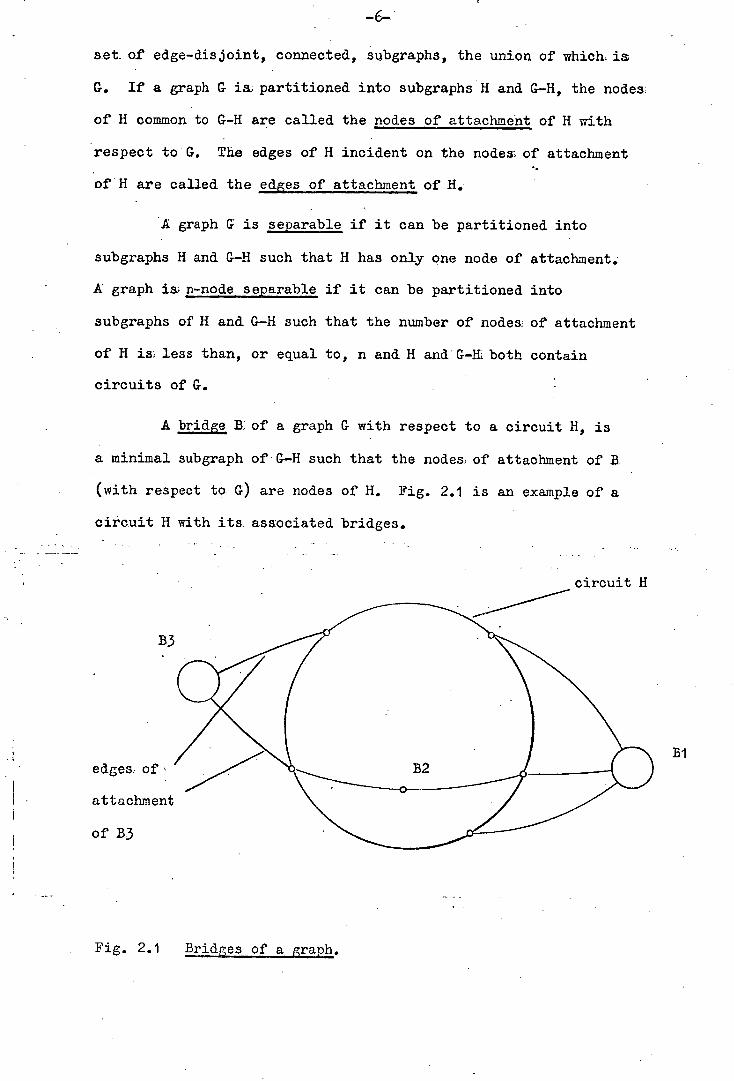
A bridge B; of a graph C- with respect to a circuit H, is
a minimal subgraph of C-H such that the nodes: of attachment of B
(with respect to C.) are nodes of H. Fig. 2.1 is an example of a
circuit H with its. associated bridges.
circuit H
edges: of'
attachment
of B3
BI
Fig. 2.1 Bridges of a graph.

-7-
2.1.2 Graph Representations.
A graph C-, without loops, may be completely described
by an adjacency matrix,
= EM..] 1J
in which, M n where n is the number of edges 1J
incident on both node i and
node j.
Fig. 2.2 is the adjacency matrix of a graph which will be
referred to as graph Cl.
vi V2 ,V3 V4 V5 V6 V7 V8
•
vi 0 1 0 0 1 1 0 0
V2 1 0 1 0 0 1 0 0
V3 0 1 0 10 0 01
V1 0 0 10 1 0 1 1
V5 1 0 0 1 0 0 1 0
V6 1 1 0 0 0 0 1 0
V7 0 0 1 1 1 1 0 0
V8 0 0 1 1 0 0 0 0
Pig. 2.2 Matrix description or Cl.

An equivalent equivalent way of describing a graph is to list the
edges with their incident vertices;. Fig. 2.3 is a description of
G1 in this form.
01 VI , V.2
e3 V3 , V4
e4 v5 , v
e5 V5 , VI
06. V7 V5
V6 , V7
08 V7,V3
09 v8,V3
e10 V8 , V11•
e
e12 VI , V6
e 13 V6, V2
Fig. 2,3 GI described aa list of edg es .
2.1.3 Planar Meshes.
A planar mesh of G is a set,
M=C 12 C2,........ck
of elementary cycles, of G, such that,

-9-
(i)
If an edge G belongs to one of the sets C it belongs
to just two of them.
(2) Any cycle of G can be expressed as a modulo-2-sum of
members; of M.
An example of a planar mesh of GI is given in Fig. 2.1 4 ,
MA = I c1 , c 2 , c3, c, c 5 , c61 c 7
where,
C1 = e, e3 , e 1 , e5 , e
c2 = e, e 8 , e 7, e13 }
C3 = {e 1 e13 , e12}:
= k l 2, e6, e7, e5
C5 = . e8 , e11 , e9 , e10
C6 =- {.i-' e11 , e6
C7 =, {e9 e10 , e3
Fig. 2.4 A Planar MesMA of C-I.
It can be seen that MA satisfies condition (i) for planar
meshes. If, by referring to Fig. 2.3 we select any cycle of GI,
say,
C = .{e11 , e7, e 2 , e3, 13+3'
then C may be expressed as,
C = Mothlo-2-sum C C5, C7
e4
V
I
By repeating repeating this process for all the cycles of GI it can
be shown that MA satisfies condition (2) for planar meshes.
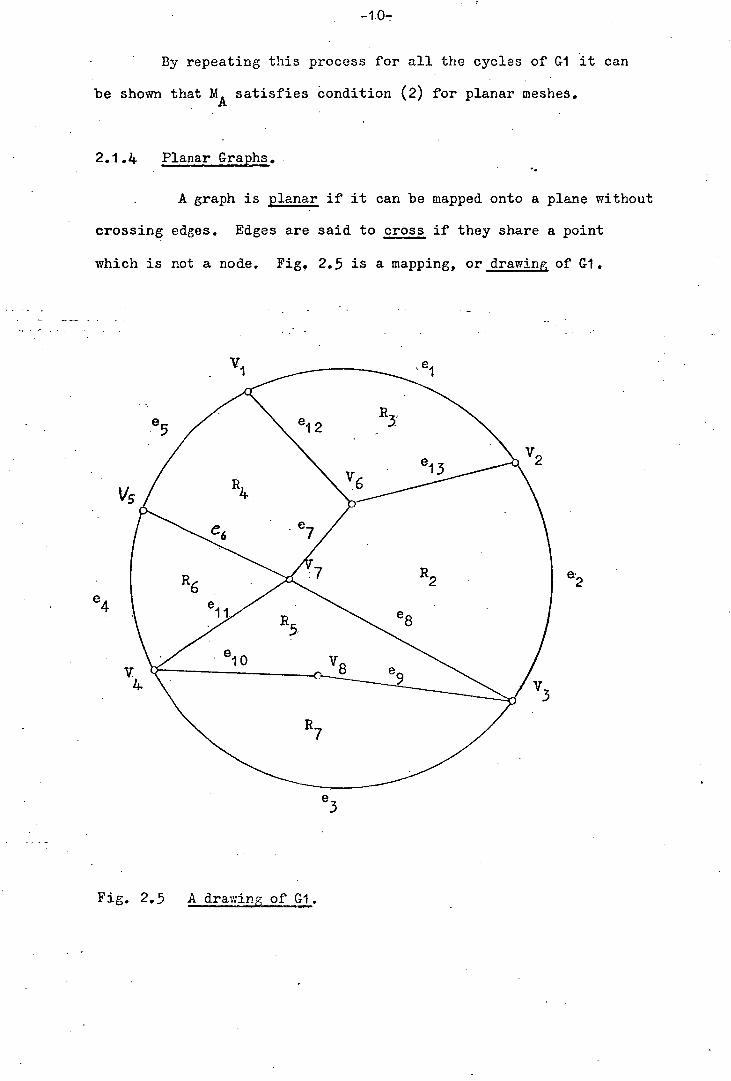
2.1 .k Planar Graphs.
A graph is planar if it can be mapped onto a plane without
crossing edges. Edges are said to cross if they share a point
which is not a node. Fig, 2.5 is a mapping, or drawing of Cl.
V. e.
e3
Fig. 2.5 A drawing of Cl.

The drawing is planar, therefore CI is a planar graph.
It is important to distinguish between a planar graph, and a
planar mesh. Tutte 120 j has shown that the necessary and
sufficient condition for a graph to be planar is that it contain
a planar mesh. However, a graph may contain more than one planar
mesh. Ore 114 J has shown that the necessary and sufficient condition
for a connected, non-separable, planar graph to have only one
planar mesh is that it does not contain a 2-node-separation. It
would appear that the number of planar meshes of a connected,
non-separable, planar graphGis equal to twice the number of
2-node-separations of G.
A planar mesh may be drawn on a plane such that any one
of its elementary cycles defines the infinite region. Thus, the
number of topologically distinct drawings of a connected, non-
separable, planar graph, C, is equal to the total number of
elementary cycles of the planar meshes of C.
To illustrate the above points Fig. 2.5 is a drawing of
the planar mesh of C-I in Fig 2.4 in which C1 has been chosen to
define the infinite region. It may be observed that Ci has only
one 2-node-separation, the subgraphs being,
HI £e9, e10, e3 , v3 , v, v8
and, C-I - HI. Thus, CI would appear to have only two planar meshes
and since there are seven elementary cycles the total number of
topologically distinct drawings of C-i is fourteen.
-12-
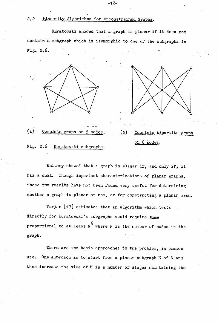
2.2 Planarity Algorithms for Unconstrained Graphs.
Kuratowski showed that a graph is planar if it does not
contain a subgraph which is isomorphic to one of the subgraphs in
Fig. 2.6.
(a) Complete graph on 5 nodes;. (b) Complete bipartite graph
on 6 nodes, Fig. .2.6 Kuratowski subgra phs.
Whitney showed that a graph is planar if, and only if, it
has a dual. Though important characterisations of planar graphs,
these two results have not been found very useful for determining
whether a graph is planar or not, or for constructing a planar mesh.
Tarjan H71 estimates that an algorithm which tests
directly for Kuratowski's subgraphs would require time
proportional to at least N6 where N is the number of nodes in the
graph.
¶here are two basic approaches to the problem, in common
use. One approach is to start from a planar subgraph H of G- and
then increase the size of H in a number of stages maintaining the
planarity of of H at each stage. This approach will be called the
synthesis approach . In the other approach the graph is effectively
drawn, and then the positions of the nodes and the routes of the
edges are modified to reduce the number of edge crossings in the
drawing. This approach will be called the analysis approach.
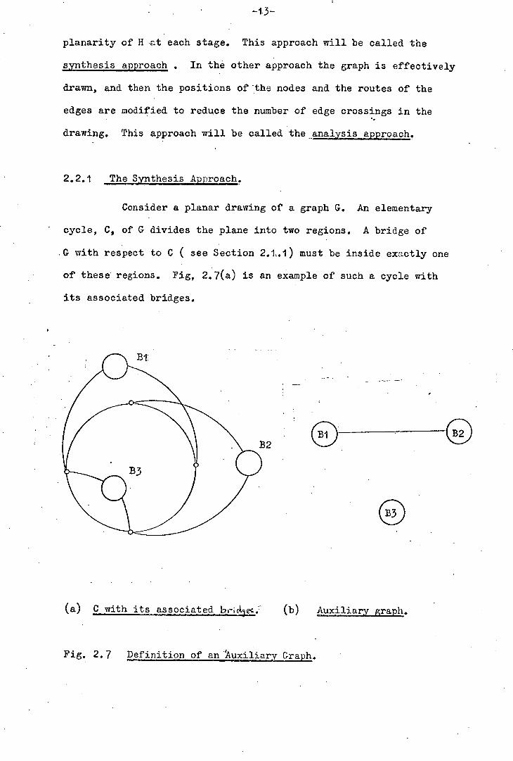
2.2.1 The Synthesis Approach.
Consider a planar drawing of a graph C. An elementary
cycle, C. of C divides the plane into two regions. A bridge of
C- with respect to C ( see Section 2.1.1) must be inside exactly one
of these regions. Fig, 2.7(a) is an example of such a cycle with
its associated bridges.
2O
(a) C with its associated br;c. (b) Auxiliary graph.
Fig. 2.7 Definition of an&uxiliary Graph.

Two bridges bridges are said to avoid each other if they may both be
placed in the same region without their attachment edges crossing
An auxiliary graph is defined by -representing bridges: of C- with
respect to C as nodes and making them adjacent only if the bridges
they represent do not avoid each other. The auxiliary graph of the
graph in Fig. 2.7(a) is shown in Fig.2.7(b).
The graph C- is planar if and only if, for every elementary
cycle C of G the nodes of the auxiliary graph can be coloured with
two colours such that no two adjacent nodes have the same colour.
A number of basic algorithms exist 'for determining the auxiliary
graphs of C- with respect to its elementary cycles.
The first method suitable for computer implementation'
which uses this approach was formulated by Goldstein L18J.
An arbitrary elementary cycle of G is selected and forms
a planar mesh, M, of a subgraph, H, of G. All the bridges of C-
with respect to H, B(H), are found. If a bridge cannot be inserted
into any region of M without causing crossing branches, C- is
non-planar, and the procedure is terminated. If a bridge may only
be inserted into one region an elementary path through the bridge
with nodes of H as its ends. is determined, and the path is inserted
into the planar mesh. The path splits a region of M to form a new
planar mesh with one more elementary cycle than M. Thus, the new
subgraph H is formed and the process is repeated. If all the bridges
may be inserted into more than one region an arbitrary choice of
region is made. Bridges consisting of a single edge are given
priority for insertion into the mesh.
Shirey 1.11] has implemented C-oldstein's algorithm and

shown that that it requires time proportional to not more than N 3. -
The algorithm can easily be adapted to construct a maximal planar
subgraph of a non-planar graph.
Bader [4] uses a simple search procedure to attain an initial-
elementary cycle with a& many edges as; possible. The search
procedure does. not guarantee to find a Hamiltonian circuit of G.
even if one exists. The elementary cycle forms the initial planar
subgraph H. The problem of determining whether C is planar or not
is then separated into two sub-problems.:
To determine whether the auxiliary graph formed by
considering the bridges B(H) can be two-coloured,
to determine if each subgraph of C. consisting of the
union of a bridge and H is planar.
If the auxiliary graph cannot be two-coloured C is non-planar.
Only subgraphs in (b) which are formed from the union of H with a
bridge containing more than one node not in H need be tested further
since other subgraphs are trivially planar.
Fisher and Wing [191 have implemented a method which is very
similar to Bader's, except that the procedure starts from an arbitrarily
selected elementary cycle and the operations are performed using
matrices. Shirey has estimated that this method has a lower time
bound of at least N4 .
Hoperoft and Tarjan [20] describe a method, again starting
from an arbitrary elementary cycle of C which forms a planar mesh,
M, of a subgraph, H of G. An elementary path with only its ends
common to H is found. If the path cannot be inserted into a region
of the planar mesh of H the graph is non-planar. If it can only
-16-
be inserted into one region the path is added to H and the region
is split to form a new planar mesh. If a path may be inserted into
more than one region, its insertion is deferred and a new path is
found. If, at any stage, all the paths may be inserted into more
than one region an arbitrary. choice is made, and a new planar mesh
created..
This algorithm has been implemented and requires time
proportional to N log N.
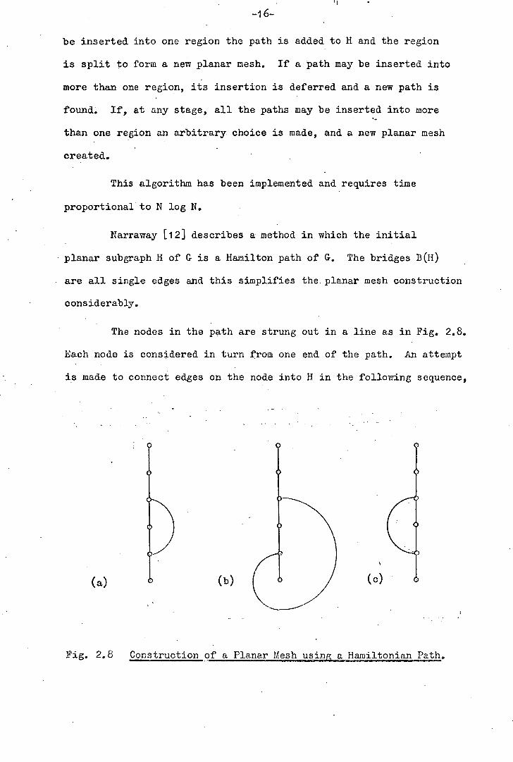
Narravray [12] describes a method in which the initial
planar subgraph H of G is a Hamilton path of G. The bridges B(H)
are all single edges and this simplifies the planar mesh construction
considerably.
The nodes in the path are strung out in a line as in Fig. 2.8.
Each node is considered in turn from one end of the path. An attempt
is made to connect edges on the node into H in the following sequence,
(a) (b) (c)
Fig. 2.8 Construction of a Planar Mesh usinR a Hamiltonian Path.
-17-
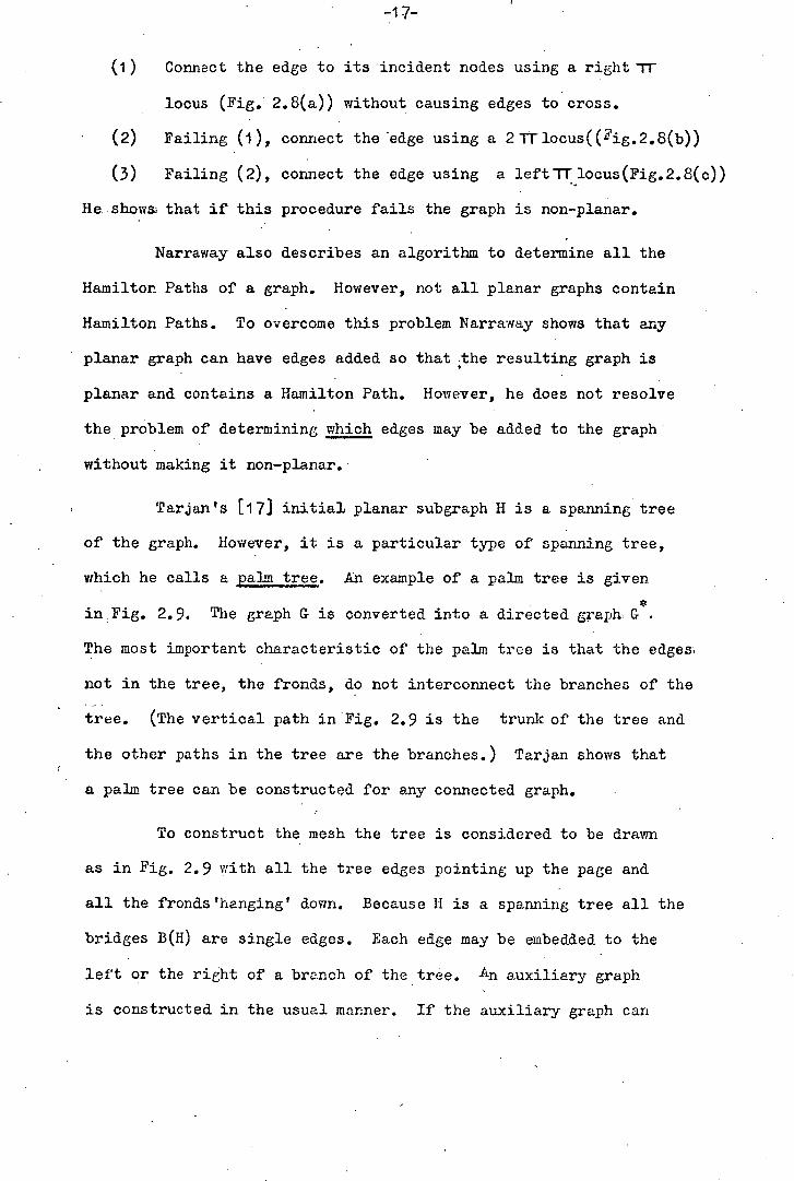
(i) Connect the edge to its incident nodes using a right TV
locus (Fig.' 2.6(a)) without causing edges to cross.
Failing (1), connect the edge using a 2lTlocus(( 2ig.2.8(b))
Failing (2), connect the edge using a leftTr locus (Fig.2.8(c))
He shows; that if this procedure fails the graph is non-planar.
Narraway also describes an algorithm to determine all the
Hamilton Paths of a graph. However, not all planar graphs contain
Hamilton Paths. To overcome this problem Narraway shows that any
planar graph can have edges added so that the resulting graph is
planar and contains a Hamilton Path. However, he does not resolve
the problem of determining which edges may be added to the graph'
without making it non-planar.
Tarjan's [17] initial planar subgraph H is a spanning tree
of the graph. However, it is a particular type of spanning tree,
which he calls a palm tree. An example of a palm tree is given
* in,Fig. 2.9. The graph G is converted into a directed graphG
The most important characteristic of the palm tree is that the edges;
not in the tree, the fronds, do not interconnect the branches of the
tree. (The vertical path in'Fig. 2.9 is the trunk of the tree and
the other paths in the tree are the branches.) Tarjan shows that
a palm tree can be constructed for any connected graph.
To construct the mesh the tree is considered to be drawn
as in Fig. 2.9 with all the tree edges pointing up the page and
all the fronds'hanging' down. Because H is a spanning tree all the
bridges B(H) are single edges. Each edge may be embedded to the
left or the right of a branch of the tree. An auxiliary graph
is constructed in the usual manner. If the auxiliary graph can
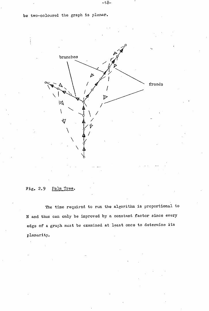
be two-coloured the graph is planar.
branches
& fronds
\
Fig. 2.9 Palm Tree.
The time required to run the algorithm is proportional to
N and thus can only be improved by a constant factor since every
edge of a graph must be examined at least once to determine its
planarity.

-1.9-
2.2.2 The Analysis Approach.
Nicholson [6] uses an approach which is superficially
similar to that proposed by Narraway [1,2] , described in Section
2.2.1. Nicholson shows that any graph can be drawn with minimum
crossings (e.g. zero, for a planar graph) with nodes on a node line
and with the edges drawn as left TT curves, right iT curves or 2 TT
curves. He also shows. that for a planar graph only left IT curves
and right iT curves are needed if the graph contains a Hamilton
circuit. To simplify the algorithm he assumes the graph contains
a Hamilton circuit.
Initially he draws the edges between the adjacent hodes.
Then, using a permutation procedure he changes the order of the nodes.
in the node line to reduce the number of edge crossings. Changes
are selected by examining the number of crossings caused by edges
incident on particular nodes.
The algorithm does not guarantee to find the minimum
number of crossings, but does find a sub-minimum. It is simple to
implement and computationally efficient for graphs with a small
number of nodes. -
2.3 Modelling a Circuit as a Graph.
Conductor tracks on a single layer of a printed circuit
board may only intersect if they are part of the same circuit net.
The similarity of this constraint to the planarity of a graph has.
led to the consideration of methods of mapping a circuit on to a graph.
It is desirable that the graph representation of a circuit
satisfy the following conditions,
-20-
(i) the graph should correspond to the graph definition in
Section 2.1.1
(2) the planarity of the graph should be the necessary and
sufficient condition for a layout to exist. with no
illegal track crossings.
If these conditions are satisfied conventional graph theoretic
algorithms may be used to test for planarity and to construct a
planar mesh which may then be mapped onto a layout without track
crossings.
There are three mappings in common use. They are discussed
by Goldstein and Schweikert EH103, and will also be discussed here.
2.3.1 Components-to-nodes and Nets-to-edg.
It may be shown that the sequence, but not necessarily
the orientation of edges incident on a node remains constant for
all embeddings of a planar mesh. If certain sequences of edges
incident on a node are not permitted for some reason then the
planar meshes requiring these sequences may not be embedded without
crossings.
Narraway shows in 12] that irrespective of the sequence
of tracks approaching a component the tracks can always be routed
to the appropriate pins provided there is no restriction on the
distances between pins. However, the space between component pins
is limited and as a result there may be a restriction on the sequence
of tracks which may approach a component. Thus, if components are
mapped onto nodes it is not in general sufficient that the graph
be planar for a layout without track crossings to exist, since it

-21-
is possible that no planar mesh of the graph may be embedded with
acceptable edge sequences.
An edge, by definition, is incident on exactly two nodes,
but a net may connect more than two components. To resolve this
problem a net is usually representeby a set of edges incident
on the nodes (components) connected to the net.
One approach is to represent a net by the edges of an
elementary path. Every node in the path, apart from the path ends,
is connected to the net by two edges. Thus, a node representing
a three pin component may have four incident edges. This imposes
a further restriction on the sequence of edges incident on a node
since it may be necessary to route track between component pins
if two edges of the same net are not adjacent in the sequence.
In addition representing a net as the edges in a path unnecessarily
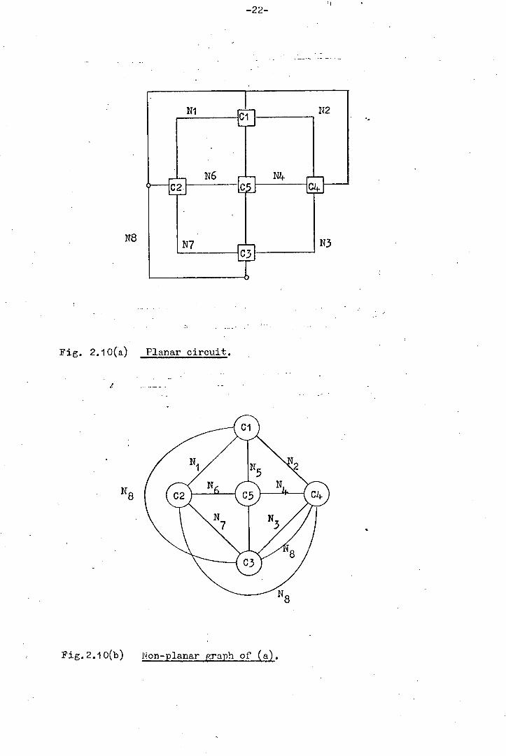
constrains the graph. This is illustrated in Fig. 2.10 (taken from
[io)). Net N8 of Fig. 2.10(a) connects ci, C2, C3, and CAF. If,
as isquite possible, N8 is represented by the edges; in a path as
shown in Fig. 2.10(b) the resulting graph is non-planar.
Kodres [5) connects an edge between every pair of nodes
in the net. In this case an even greater constraint is imposed
on the graph, and if any net connects more than four components
the graph must be non-planar.
-22-
Fig. 2.10(a) Planar circuit.
/
N8
Wj
Fig. 2.10(b) Non-planar graph of (a).
-23-.
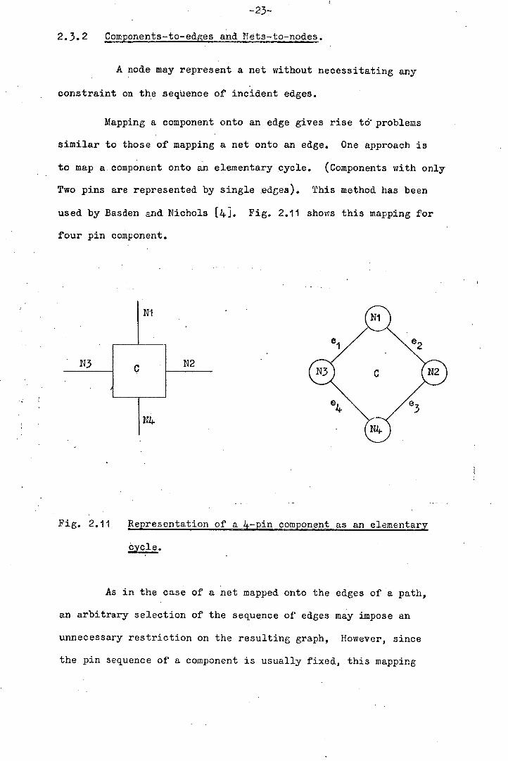
2.3.2 Components-to-edges and Nets-to-nodes.
A node may represent a net without necessitating any
constraint on the sequence of incident edges.
Mapping a component onto an edge gives rise to' problems
similar to those of mapping a net onto an edge. One approach is
to map a. component onto an elementary cycle. (Components with only
Two pins are represented by single edges). This method has been
used by Basden and Nichols [1j. Fig. 2.11 shows this mapping for
four pin component.
NI
ey
C
e4 \
Fig. 2.11 Representation of _ a 4-pin component as an elementary
cycle.
As in the case of a net mapped onto the edges of a path,
an arbitrary selection of the sequence of edges may impose an
unnecessary restriction on the resulting graph, However, since
the pin sequence of a component is usually fixed, this mapping
-24-
provides a convenient method of restricting the sequence of tracks
approaching a component.
Because the component is represented. by a cycle it is
possible for a planar mesh to be constructed in which a component
is 'upside down', or is positioned 'inside' another component.
This problem is usually overcome by restricting the sequence of edges
incident at a node such that the edges representing the same component
are always adjacent in the sequence and have the same orientation
with respect to the node.
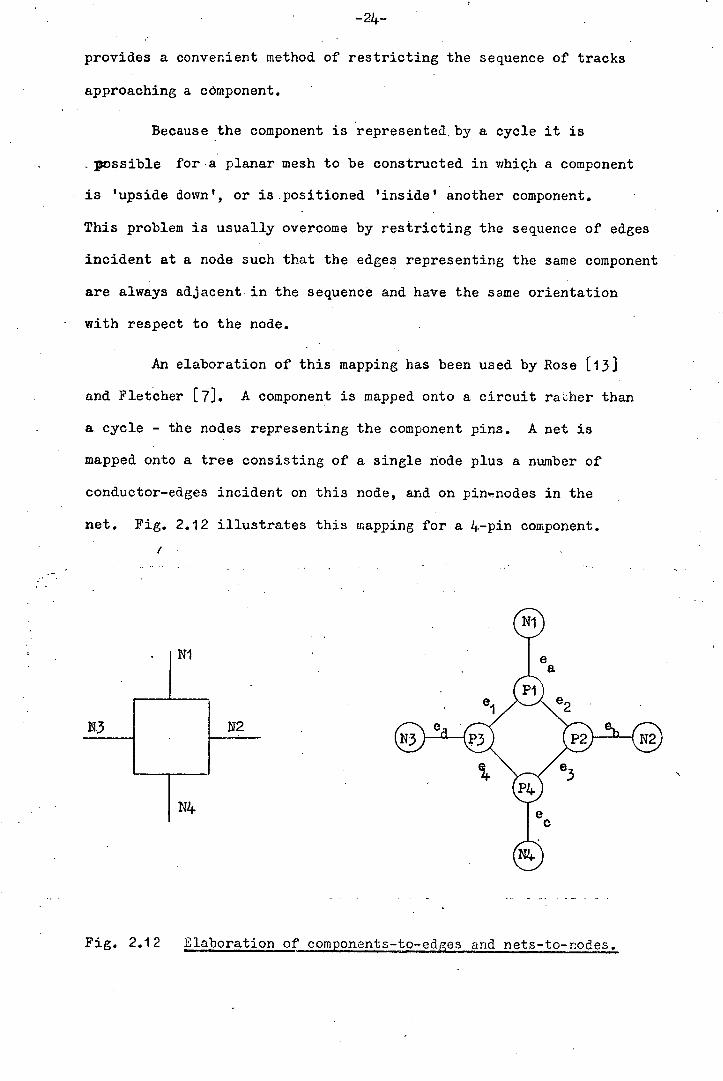
An elaboration of this mapping has been used by Rose {13]
and Fletcher [7]. A component is mapped onto a circuit rather than
a. cycle - the nodes representing the component pins. A net is
mapped onto a tree consisting of a single node plus a number of
conductor-edges incident on this node, and on pinnodes in the
net. Fig. 2.12 illustrates this mapping for a 4-pin component.
I
Fig. 2.12 Elaboration of components-to-edges and nets-to-nodes.

The edges edges ( e a, e e0, e ) are introduced to avoid the
deletion of the edges representing the component in the event of
the graph being non-planar. For example Fig. 2.13 shows two
4-pin components connected to produce a conductor cros.ing.
N2
C -P Ni N5
Fig. 213 Non planar connection of two I f-pin components.
Using Rose's method the representation would be as in Fig. 2.1If
WA
Fig. 2.14 Giph representation of circuit in Fig. 2.1.

-26-
It can be seen that the crossing can be removed by
deleting edge e'. However, if the nets are represented simply
as nodes, (as done by Basden and Nichols [.i.J) the circuit in
Fig. 2.13 could be partially represented as in Fig. 2.15. Net N2
is represented as two nodes - it has been split. If N2 were to
be represented as one node the components would overlap in the
mesh of the graph.
Fig. 2.15 2.15 littinof a node representinp a net.
In fact the representation in Fig. 2.14 is equivalent to
that in Fig. 2.10, if edge ea' is removed. Thus, in one mapping,
crossings are removed by deleting edges representing conductor track
and in the other nodes are split. (Inferring the removal of
conductor track.)
Engi 13] generalises the concept of an'edge so that it may
be incident on any number of nodes.. These generalised edges he
calls spiders. Nets are mapped onto nodes and components onto
spiders. If a component has more than three connections then the
connected nodes are joined into a circuit by two-legged spiders
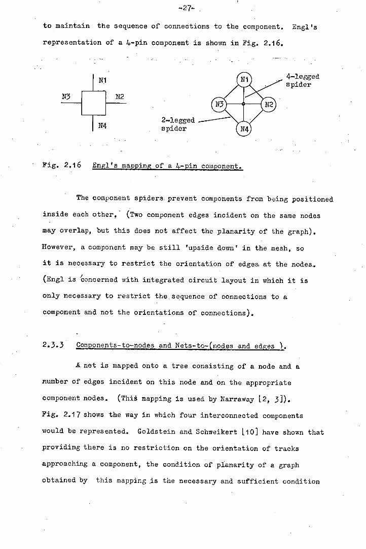
-27-
to maintain the sequence of connections to the component. ing1's
representation of a if-pin component is shown in Fig. 2.16.
Ni
N31 1N2
2-legged N4 spider
4-legged spider
Fig. 2.16 Engi's mappingof a if-pin component.
The component spiders prevent components from being positioned
inside each other, (Two component edges incident on the same nodes
may overlap, but this does not affect the planarity of the graph).
However, a component may be still 'upside down' in the mesh, so
it is necessary to restrict the orientation of edges at the nodes.
(Engi is 'concerned with integrated circuit layout in which it is
only necessary to restrict the sequence of connections to a
component and not the orientations of connections).
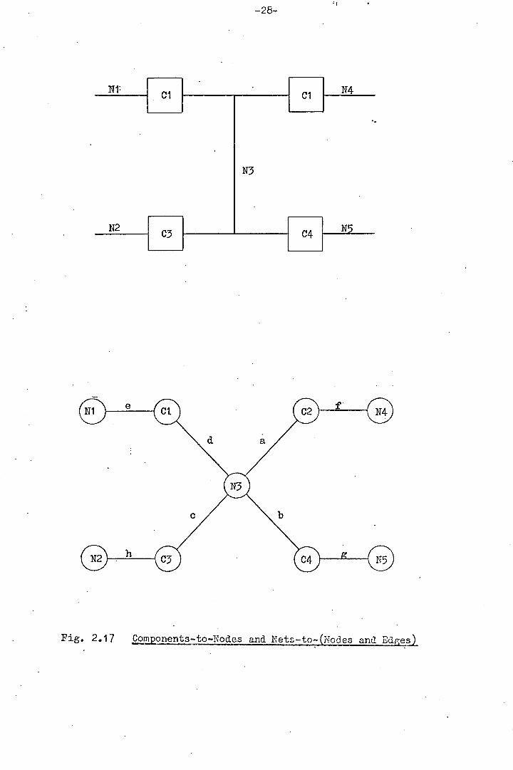
2.3.3 Components-to-nodes and Nets-to-(nodes and edges.
A. net is mapped onto a tree consisting of a node and a
number of edges incident on this node and on the appropriate
component nodes. (Thig mapping is used by Narraway [.2, 3]).
Fig. 2.17 shows the way in which four interconnected components
would be represented. Goldstein and Schweikert 1.iO] have shown that
providing there is no restriction on the orientation of tracks
approaching a component, the condition of planarity of a graph
obtained by this mapping is the necessary and sufficient condition
-28-
Fig. 2.17Components-to-Nodes and Nets-to-(I'roc1.es and EgsJ

-2.9-
for a layout to exist with no track crossings. However, the
orientation of tracks: approaching a component is usually restricted
and therefore, in the general case, the planarity of a graph is not
a sufficient condition for a valid layout to exist.
2.4 Planarity. Algorithms for Circuit Graphs.
If components and conductors have a graph representation
as edges the planarity constraint may be relaxed to allow
conductors to pass between component pins. In addition, conductor
edges may be allowed to cross each other if one of them is replaced
by a wire-jumper in the layout. Thus, a circuit graph may be
non-planar, and yet be realisable as a layout.
The circuit graph may also be modified so that it represents
the same circuit, and yet has different planarity characteristics.
E.g. a conductor may be routed between the pins of a component by
splitting a conductor edge into two, and making the resulting edge
incident on the corresponding component node. Thus, the problem
of constructing a mesh (not necessarily planar), which may be
realised as a layout, is dependent on the technology being used,
and, consequently, is not EL& well defined as the related problem
of determining whether a given graph is planar or not.
A number of algorithms have been proposed to construct a
mesh of a. circuit graph.

-30-
The main requirements of an algorithm are,
(i) the mesh should be realisable as a valid layout,
within the limits of the technology the mesh should
contain the minimum of wire-jumpers,
the algorithm should be suitable for computer implementation,
the algorithm should be computationally efficient.
The most significant algorithms will now be discussed in
relation to these requirements.
Kodres 1.53 describes a method to obtain more than one
layer of interconnections for double sided or multilayer boards.
A component is represented by a node, and a net is represented by
the complete graph on the nodes of the net. Each edge is given
a weight inversely proportional to the number of nodes in the net.
The edge connector terminals are represented by nodes and are joined
into .a circuit to form the perimeter of the board. The nodes. of
this circuit are drawn on a circle in a plane. The remaining nodes
are positioned using a Centre of Gravity technique which takes
account of the weights of the edges connected to a node. A minimum.
length spanning sub-tree of each net is determined, in which the
length of an edge is made proportional to the number of edges it
crosses. Since the components are represented as nodes, crossings
induced by the incident sequence of a node differing from the pin
sequence of a component are included in the calculation of edge
lengths. Thus, an attempt is made to reduce.. the number of conductor
crossings in the drawing. An auxiliary graph is constructed in which
the nodes correspond to the edges of the drawn graph, and two nodes
are adjacent if the edges they represent cross each other in the

drawing. The The auxiliary graph is then two-coloured, removing
the minimum number of edges. The two colours represent the two
layers of interconnections of thö board. The last stage in the
procedure is to try to insert any rejected edges, using the spaces
between component pins.
The effectiveness of Kodres' method is not known since the
method had not been implemented at the time of its publication,
and no further reference to it has been found.
A detailed description and discussion of Rose's method [13]
of constructing a mesh of the circuit graph is given in Sections.
3.1.2 and 3.1.3 of chapter 3. The basic approach used is to separate
the mesh construction into two stages,
(i) construct a planar mesh of a subgraph of the circuit graph
which satisfies the constraints on edge orientation etc.,
(2) insert rejected edges -.using the interpin spacing of
components..
The planar mesh is constructed using a methoci very similar
to that of Hoperoft and Tarjan [20] des:cribed in Section 2.2. The
most important difference is that a region is selected, and then
an elementary path is sought which has nodes on the region
boundary as its ends instead of finding an elementary path
between any two nodes in the mesh, and then searching for regions
in which to insert it.
Fletcher [7] uses a circuit graph mapping which is very
similar to that used by Rose, in vhich a component is mapped onto
a circuit, and a net is mapped onto a single-node-tree. The
board edge is mapped onto a circuit in which the nodes represent

-32-
the edge connector terminals, and the edges represent the board
perimeter.
The first stage in constructing the mesh is to definp a
planar mesh containing one elementary cycle consisting of the edges
in the edge connector circuit. A spanning tree of the circuit
graph is found ignoring the edges in the planar mesh. The paths
through the tree with ends as terminal nodes are inserted into the
planar mesh to form a new planar mesh. This is illustrated in
Fig. 2.18.
board
perimeter
terminal
nodes
U
Fig. 2.18 Planar mesh after insertion of paths of spannin tree.

-33-
Branches of the tree .not connected into the mesh (indicated
with dotted lines in Fig.2.18 ) are not fixed in any region at
this stage.
The bridges of the circuit graph, with respect to the mesh
subgraph must now be added to the mesh. Each edge not in the tree
is considered in turn. If the edge is incident on two nodes of
the same branch which has not yet been inserted into a region, its
insertion is deferred. Otherwise an elementary path is found with
ends in the mesh subgraph, the object being to split a region of
the existing planar mesh to form a new planar mesh. If such a
path cannot be inserted without causing crossing edges, the edge
not in the tree is temporarily deleted. If the path can only be
inserted into one region, it is immediately added to form a new
planar mesh. If the path can be inserted into more than one region
it is suggested that one of the following strategies might be used,
(i) the choice of region be deferred (as done by Koperoft
and Tarjan t201),
the circuit graph be examined, 'to enble.a rational
choice to be made',
an arbitrary choice of region be made.
Temporarily deleted edges are inserted by allowing conductor
edges to cross component edges, if the pin spacing permits, or
other conductor edges inferring the use of wire-jumpers. The
choice of technique used to insert a pAth is determined by a cost
which relates the use of a number of component crossings to the
use of a wire-jumper.
-347
It is not clear how Fletcher prevents components being
reflected, or placed inside each other without additional constraints
being imposed on the-path-searching procedure.
An effort is made in the method to minimise the number of
component crossings by exploiting the planarity characteristics
of the circuit graph. This is done to leave routes between component
pins open for conductors which might otherwise have to be wire-
jumpers in the layout.
It is not possible to determine from Fletcher's description
whether the algorithm is effective or not, though it would appear
to be suitable for computer implementation.
Narraway 131 suggests that the algorithm for constructing
a planar mesh, using a Hamilton Path, (described in Section 2.3 )
could be extended to a graph representing a circuit. He uses the
same circuit- graph mapping as Fletcher, in which components are
mapped onto cycles and nets are mapped onto trees.
It is assumed that the planarity of the circuit graph is
the sufficient condition for a valid layout to exist. This is false,
since all of the planar meshes of the circuit graph may require some
components to be upside down, or placed 'inside' each other.
However, it would appear that the algorithm could easily be
modified to restrict the sequence of edges incident at a node, and
hence prevent such conditions occuring.
The method is very simple and would appear to be
computationally efficient. The extent to which the number of
wire-jumpers can be minimised is largely dependent on whether a
Hamilton Path can be found or not. If a Hamilton Path is
-3.5-
constructed by adding edges to the circuit graph a more complicated
algorithm must be used to avoid unnecessary deletion of edges.
Basden and Nichols 1121 use the basic mapping of components
to edges,.and nets to nodes. Components with more than two pins
are represented by the edges of an elementary path, or cycle.
An initial planar mesh is constructed using a cycle of edges
incident on nodes representing the nets connected to the edge
- connector terminals. Each component is inserted individually into
a region of the planar mesh. In order to decide in which region
to insert a component, the regions are weighted as follows,
the weights of all regions are set to zero,
the weights of the regions around each node to which the
component must be connected are increased by one,
(o) the weights of the regions one edge removed from each
node are increased by two,
(d) etc., etc.
The component is inserted into the region with lowest
weighting. (It is not slear what happens if there is more than one
region with the lowest weighting). This procedure minimises the
number of component crossings necessary to insert a p articular
component. The component is inserted into the region by merging
each node joining the component edges with the corresponding net-
node in the mesh. (If the latter exists). If a node is to be merged
with a node which does not bound the region in which the component
is inserted, then one of the following strategies is used,
-36.-
the node is 'moved onto' component edges until the nodes
may be merged,
nodes are split until the nodes to be merged both lie
on the boundary of the same region.
(a) corresponds directly to routing a conductor between
the pins of a number of components. Though described as 'moving
a node onto an edge', in graphical terms this means the component
edge is split into two edges, and the degree of the node is
increased by two i.e. the circuit graph is changed.
The action of (b) is to take out one or more conductors
to insert another conductor.
Strategies (a) and (b) are used alternately until all the
possible connections have been made to a component. The nodes
which have been split using (b) are then reconnected using (a)
if it is possible, otherwise a wire-juniper must be inserted.
The effectiveness of the algorithm has yet to be proved.
It would seem that the planarity characteristics of the circuit-
graph are not fully exploited by the method.
A great deal of dependence is put on the use of interpin
spacing, and thus, a large number of wire-jumpers may be required
for large circuits. It is not clear how the procedure of splitting
nodes may be controlled effectively without the use of manual
interaction.
The graph representation used by Engi [91 is described in
Section 2.3.
Engi formalises the concept of modifying a circuit-graph
-3.7-
to make use of the technology-by defining two transformation
operations which may be applied to the graph. One operator splits
a node into two new nodes, which together have the same edges
incident on them as on the original node. The other operator
deletes a spider-leg from the graph. The application of either
operator creates a new graph, with different planarity characteristics.
It is obvious that any graph can be made planar by the repeated
applications of these operators.
Because a large number of planar graphs can be obtained
by applying these operators, Engl suggests that a particular planar
graph be selected interactively. It is not clear how much of the
planarising can be done manually, and how much automatically.
2.5 Methods of Transforming a Mesh into a Layout.
Very few methods of transforming a mesh into a printed
circuit layout have been proposed, and even fewer have been
implemented..
Rose [13] has implememted a method which actually produces
layouts. A detailed description and discussion of the method is
given in Chapter 3..
Fletcher gives an outline description of a proposed method
in [7). In the mesh the components are represented by a circuit
of nodes and edges. (Edges representing conductors may cross the
component edges in the mesh). This component representation is
contracted to a single node with conductor edges incident on it.
Thus, in the resulting graph a component is represented by a
node and a net is represented by a node with a number of incident
-38--
edges.
It is assumed that the printed circuit board has an edge
connector along one edge only. The mesh (with components as nodes)
is drawn by 'growing' through the mesh from the nodes representing
the edge connector terminals, which are positioned along the base
of the board. Thus, each node is given a position. When this is
completed a minimal spanning tree is constructed for each net.
It is proposed then that this drawing be operated on using
a force field technique which maintains the planarity of the mesh,
and takes account of the component dimensions, but not the
component orientations. This rough layout is plotted for inspection
and modified if it appears that a detailed placement is likely to
fail. Each component is then positioned taking account of the
space required for conductors to be routed to the component pins,
and finally the conductors are routed. Because the description
is 'sketchy' (as stated by Fletcher) it is impossible to make any
statements about its effectiveness.
Kodres method I.5J is directed at printed circuits with more
than one layer of interconnections, in which the components are
positioned in a rectangular array of locations. A number of
stacked planar meshes are constructed (described in Section 2.2 )
By drawing the circuit graph and then splitting it into planar
subgraphs, representing the connections to be made on each plane.
The components are represented by nodes, and the, nets by minimal
spanning sub-trees of the nodes in each net. In order to transform
the drawing into a layout, a piecewise-linear transformation is
used. The board surface is divided into a grid in which each grid
point corresponds to a component location. The drawing is: then

-3.9-
transformed such that each component node is positioned on a arid
point, and each conductor edge (a straight line in the drawing)
is a polygonal path along grid lines. Kodres shows that a drawing
of a planar mesh, with edges as straight lines maps onto a planar
graph consisting of polygonal edges using this transformation.
After the transformation of each planar subgraph the
positions of the components is determined and the conductors approach
the components at the correct orientation. The detailed routing
of conductors to pins is not described..
-40-
Chapter 3 Rose's Layout Method.
Rose's' method is directed at the layout of single sided
printed circuit boards i.e. boards with components placed on one
side of the board and conductors routed on the other. It is assumed
that the board is rectangular with an edge connector along one
board edge, and that components may be placed anywhere within the
board area.
The method splits the problem into two separate problems.
The first problem is to construct a mesh representation of the
circuit, and the second is to realise a layout using this mesh.
This chapter contains a description of Rose's layout
method and the way in which the resulting computer aided design
system may be used. The results obtained using the system are
discussed in chapter 5.
3.1 Constructing a Mesh.
Before constructing a mesh it is necessary to define the
way in which the circuit is to be represented as a graph. The
graph representation used by Rose is described in Section 3.1.1.
The mesh is constructed in two stages,
A planar mesh of a subgraph of the graph representing
the circuit is constructed,
edges of the graph not in the planar mesh are added by
making use of the space between component pins.
The methods used to perform (i) and (2) are described in
Sections 3.1.2 and 3.1.3. respectively.

-41-
3.1.1 The Graph Representation.
As described in Section 2.2.1 the basic approach used by
Rose is to map nets onto nodes and components onto edges.
A component with only two pins is mapped onto--a single edge
termed a component branch. Such a component is termed a branch component.
A component with more than two pins is mapped onto an elementary
cycle of edges which are termed pseudo branches. Such a component
is called a subgraph component. Fig. 3.1 shows the way in which
the two types of components are connected in the graph. CI, C2,
and C4 are branch components and C3 is a subgraph component. Branch
components are connected to a net by making them incident at a
circuit node, e.g. CI and C4 are both incident at NI. Instead of
indicating the connection of a subgraph component to a net by
making its pseudo branches incident on a node, the node is, in
effect, split into a circuit node and a subgraph node connected
by a link branch. Pseudo branches are only incident on a subgraph
node. If, as will be described later, a circuit node is split into
two parts then an additional branch is used to connect the two parts
together. This type of branch is called a conductor branch. Thus,
a net of a circuit is represented in the graph as a tree consisting
of parts of circuit nodes, conductor branches, link branches and
subgraph nodes.
The edge connector terminals are generated by circuit nodes
and the sequence of terminals is fixed by connecting pseudo branches
between them, forming a ring which represents the perimeter of the
board.
Thus, in Rose's graph representation there are two-types
of node and four types of branch. -

-12- *
pseudo subgraph
branches nodes
circuit
C2
C1 C4 zT®. Fig. 3.1 The graph representation.

3.1.2 Constructing a Planar Lesh.
The basic approach used by Rose to construct a planar
mesh is described in Section 2.4. The mesh is constructed in a
series of step3i During each step an elementary cyclé of a
planar mesh of a subgraph of the circuit graph is split into two
elementary cycles to form a new planar mesh of a larger subgraph.
This procedure is repeated until no elementary cyle may be split
to form a new planar mesh. The remainder of this section is a
description of the way in which Rose has used this approach.
The first planar mesh has only one elementary cycle which
consists of the pseudo branches incident on the circuit nodes
representing the edge connector terminals. When drawn this
planar mesh defines two regions. Because the pseudo branches
represent the perimeter of the board, one region represents the
board area, and the other the area of the plane outside the
board perimeter. Only the region representing the board area may
be split to form a new planar mesh. The region which is
considered for splitting at any stage in the procedure is called
the free relon. The initial planar mesh of a circuit with three
edge connector terminals is drawn in Fig. 3.2.
The first step in splitting the free region is to find a
path which is disjoint with respect to the current planar mesh
subgraph except for its end nodes which are on the circuit defining
the free region. Such a path is termed a planar path. A node on
the free region circuit is said to have free branchei, if there are
branches incident on it which are not already part of the mesh,
and not marked as non-planar branches. The search for a planar
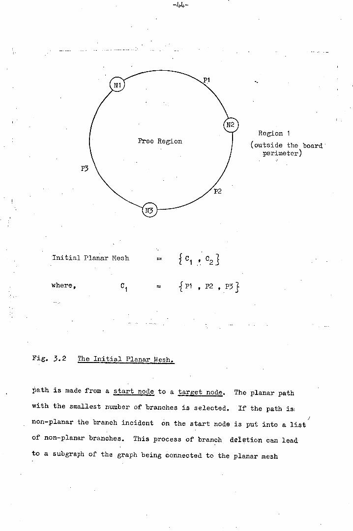
-44
P3
Region 1
(outside the board perimeter)
Initial Planar Mesh
where, C
= {e C 2 = {i ,P2 ,P3
Fig. 3.2 The Initial Planer Mesh.
Path is made from a start node to a target node. The planar path
with the smallest number of branches is selected. If the path is
non-planar the branch incident on the start node is put into a list I
of non-planar branches. This process of branch deletion can lead
to a subgraph of the graph being connected to the planar mesh

-.14.5-
subgraph by only one branch. Such a branch is termed a bridge branch
and is not allowed, to be deleted. The subgraph is connected, into
the mesh and forms part of the free region boundary.
A flow diagr'm of Rose's algorithm taken from [13] is
shown in Fig. 3.3.
If a planar path containing branches of a subgraph
component is selected the whole of the subgraph is inserted into
the mesh at once.
3.1.3 Inserting Rejected Branches.
At this stage in the method a planar mesh has been
constructed, and there is a list of rejected component branches and
link branches. The objective, now is to insert all the rejected
branches into the mesh by making use of the space between component
pins. However, since it may not be possible to insert all the
rejected branches, the component branches are given priority
because link branches maybe inserted as wire jumpers in the final
layout. Each branch is inserted independently of the other rejected
branches. A brief description of the method of insertion of the
two branch types follows.
Insertion of Component Branches.
Component branches are inserted, 'over' conductor branches.
A conductor branch is created by splitting a circuit node. The
number of conductors which may cross a component is limited by the
space between the component pins. For this reason the number of
conductor crossings required to insert a particular component is
minimised. If there is insufficient space between the

- -.-46-
co
into initial region nnector Start
Construct edge
: free region
Select a start node on the edge
of the free region
Select target node in an alcw direction
and search for planar region
Add new region
to mesh
there a planarpath_?)
J Select target node in a cw direction
and search for planar region
Add new region
to mesh
Is there a planar path_?}
i N
N Are the free branches on the
start node bridge branches ?
Add the branches] to the non- I—C 0
nnect the branches into the meshar
Are there any free branches remaining
In the free region ?
End —Jdd free region to planar mesh
Fig. 3.3 Planar mesh algorithm.
7-
component pins for the minimum number of conductors to cross, the
component cannot be placed in the layout.
Insertion of Link Branches.
Link branches are inserted 'under' components, or the
pseudo branches of subgraph components. The number of conductor
crossings is minimised for a particular branch insertion to leave
as much space between pins as possible for further branches to be
inserted. If a route between component pins cannot be found for
the link branch it may be inserted as a jumper wire in the final
layout.
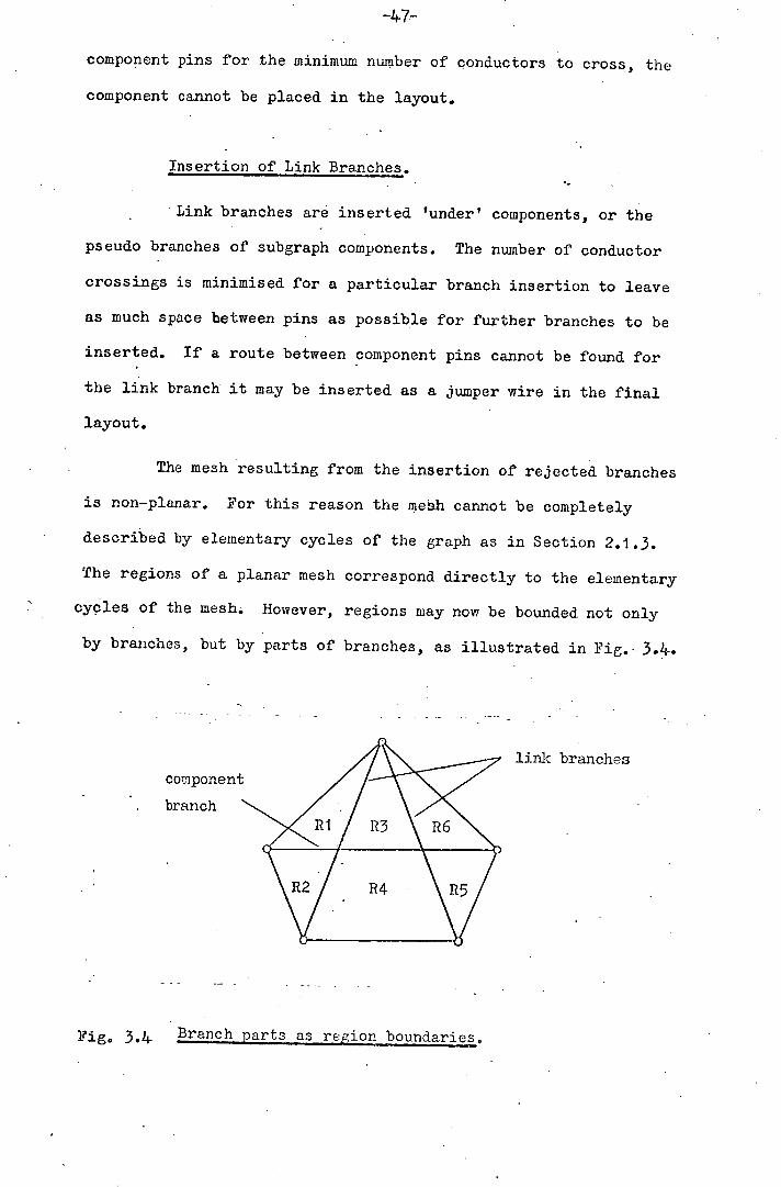
The mesh resulting from the insertion of rejected branches
is non-planar. For this reason the meSh cannot be completely
described by elementary cycles of the graph as in Section 2.1.3.
The regions of a planar mesh correspond directly to the elementary
cycles of the mesh. However, regions may now be bounded not only
by branches, but by parts of branches, as illustrated in Fig.-3.1+.
coisponeni
branch
link branches
Fig. 3.4 Branch parts as region boundaries.
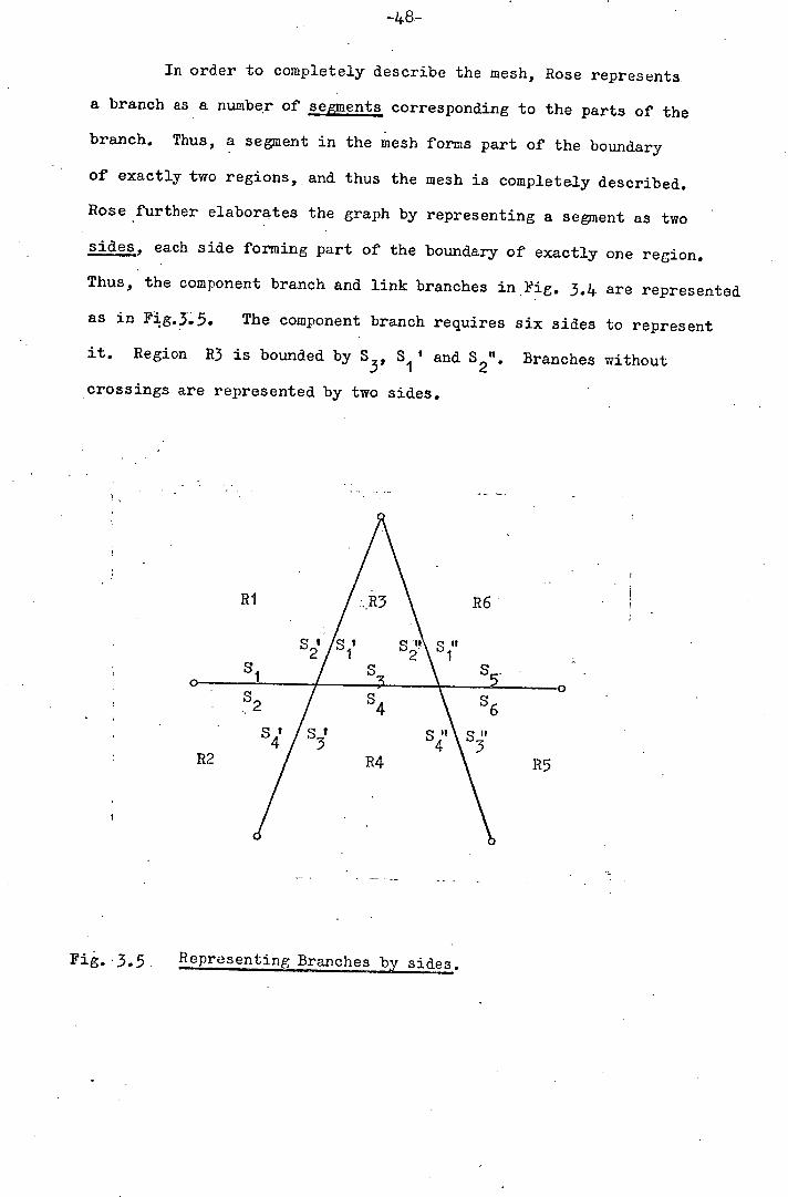
In order order to completely describe the mesh, Rose represents,
a branch as a number of segments corresponding to the parts of the
branch. Thus, a segment in the mesh forms part of the boundary
of exactly two regions, and thus the mesh is completely described.
Rose further elaborates the graph by representing a segment as two
sides, each side forming part of the boundary of exactly one region.
Thus, the component branch and link branches in lig. 3.4 are represented
as in Fig,5.5. The component branch requires six sides to represent
it. Region R3 is bounded by S 3 , S 1 f and Branches without
crossings are represented by two sides.
Fig. .3.5. Representing Brancheyides.

3.2 Transforming the }iesh into a Layout..
There are three basic restrictions which must be adhered
to when transforming the mesh into a layout,
that components must not overlap,
that track clearances be maintained to avoid illegal
electrical connections,
that the layout corresponds directly to the mesh.
The first two restrictions are obvious and apply to most
printed circuit layouts. The third restriction implies that there
should.be a 1:1 correspondence between the regions of the mesh,
other than the subgraph regions, and the areas defined by the conductors
and components of the layout. Thus, if a conductor branch crosses
a component branch in the mesh the corresponding conductor must
cross the same component in the layout.
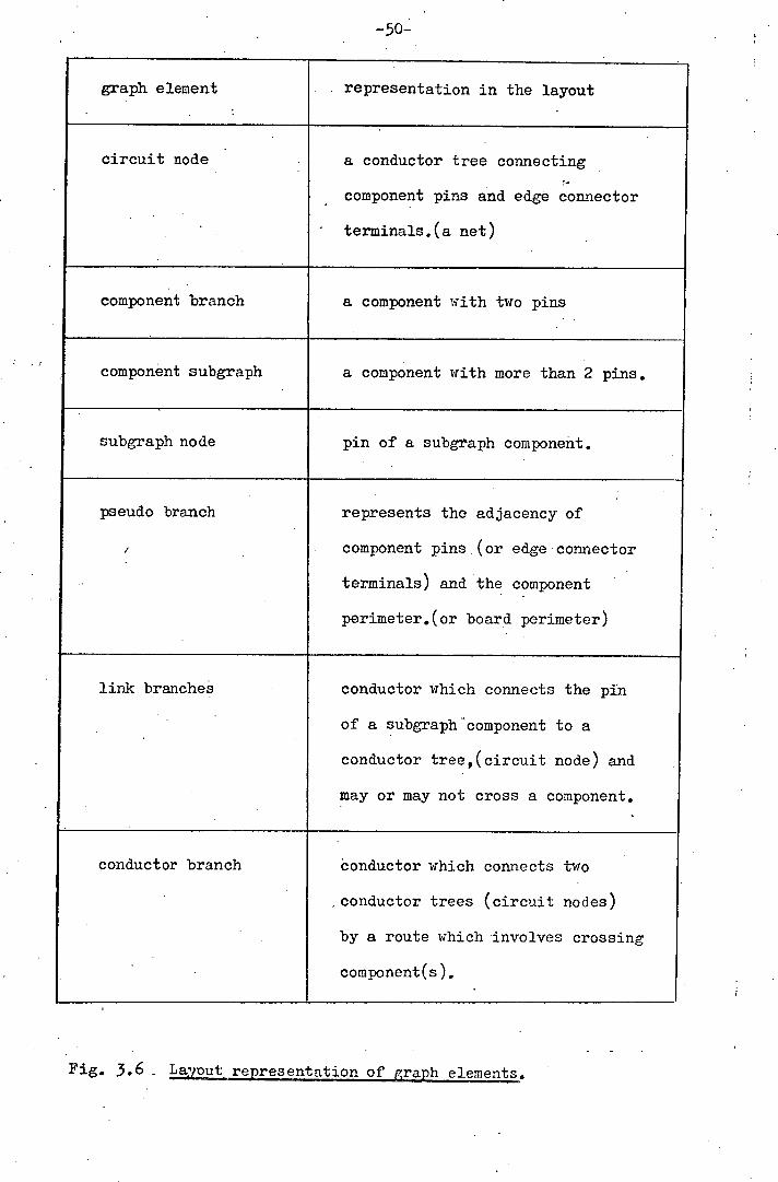
The layout representation of each element of the graph is
given in the table in p63.6.
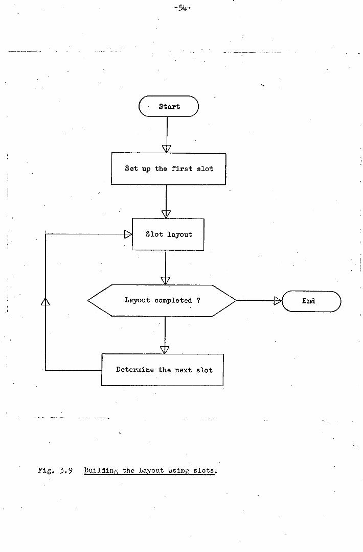
3.2.1 The Layout and the Slot.
The Layout problem is simplified by, separating it into
a number of smaller and more restricted layout problems. This;
simplified layout is constructed within an area termed a slot.
A slot is equivalent to a rectangular printed circuit board with
an edge connector along its base, but with no restriction on the
height of the board.
The rules for layout within a slot are the same as for
the complete layout with the additional constraint that no part
-50-
graph element representation in the layout
circuit node - a conductor tree connecting
component pins and edge connector
terminals.(a net)
component branch a component with two pins
component subgraph a component with more than 2 pins.
subgraph node pin of a subgiaph component.
pseudo branch represents the adjacency of
/ component pins (or edge connector
terminals) and the component
perimeter.(or board perimeter)
link branches conductor which connects the pin
of a subgraph 'component to a
conductor tree,(circuit node) and
may or may not cross a component.
conductor branch conductor which connects two
conductor trees (circuit nodes)
by a route which involves crossing
component(s).
Fig. 3.6 - out representation of graph elements.

-5.1-
of any component in the slot may have the same x-coordinate as
Any other component is the slot. Thus, the components are placed
in a strip across the slot.
The layout is started by making the first slot area
bounded by the base and the edges of the printed circuit board.
When the. layout of the first slot is completed the base of the next
slot is formed by the lowest upper edge of a placed component.
The edges of the slot are defined by adjacent components or the
edges of the board. This sequence is illustrated in Figs 3.7 and 3.8
(a) - (d). The slot 'edge connector' of the remaining slots is
formed by projecting conductors up from below the base of the slot.
The flow diagram in Fig. 3.9 shows the basic relationship between
the Slot and the Layout.
The layout of a slot is done in the following sequence
of steps,
(i) determine the possible contents of the slot,
select the components to be placed in the slot,
place the selected components and conductor ends,
route the conductors.
A description of the methods used in each step is given
in the following sections of. this chapter.
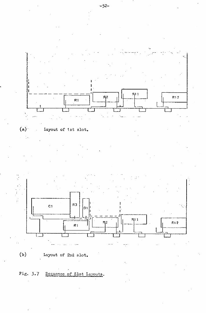
-52-
Layout of 1st slot.
(b)
Layout of 2nd slot.
Fig. 3.7 Scquence of Slot Layouts.
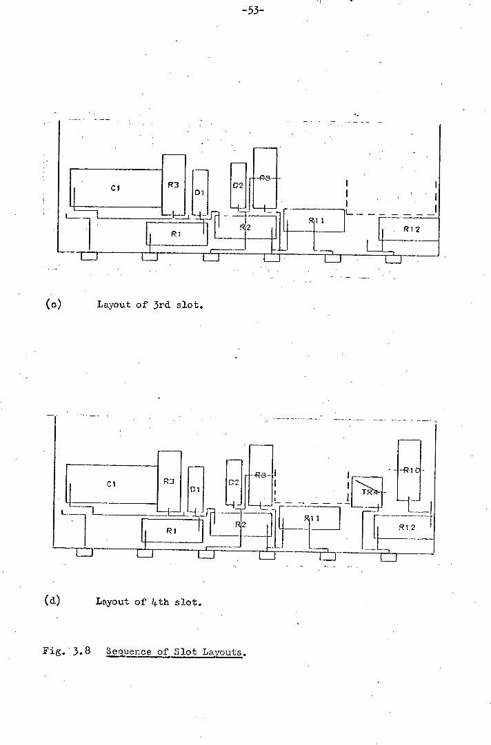
L
I -
(0)
Layout of 3rd slot.
-5.3-
(d) Layout of )+th slot.
Fi.3.8 Sequence of Slot Layouts.
-51+-
Fig. 3.9 Building the Layout using slots.
-55-
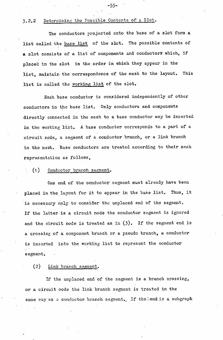
3.2.2 Determining the Possible Contents of a Slot.
The conductors projected onto the base of a slot form a
list called the base list of the slot. The possible contents of
a slot consists of a list of components and conductort which, if
placed in the slot in the order in which they appear in the
list, maintain the correspondence of the mesh to the layout. This
list is called the working list of the slot.
Each base conductor is considered independently of other
conductors in the base list. Only conductors and components
directly connected in the mesh to a base conductor may be inserted
in the working list. A base conductor corresponds to a part of a
circuit node, a segment of a conductor branch, or a link branch
in the mesh. Base conductors are treated according to their mesh
representation as follows,
(i) Conductor branch segment.
One end of the conductor segment must already have been
placed in the layout for it to appear in the base list. Thus, it
is necessary only to consider the unplaced end of the segment.
If the latter is a circuit node the conductor segment is ignored
and the circuit node is treated as in (3). If the segment end is
a crossing of a component branch or a pseudo branch, a conductor
is inserted into the working list to represent the conductor
segment.
(2) Link branch segment.
If the unplaced end of the segment is a branch crossing,
or a circuit node the link branch segment is treated in the
same way as a conductor branch segment. If the'-:end is a subgraph

-56-.
node and the subraph component has not already been placed in the
layout, then the subgraph component is inserted in the working list.
If the subgraph component has been placed , a conductor representing
the link branch segment is inserted.
(3) Part of a circuit node.
Because a branch is incident on two nodes, two branches
incident on the same circuit node.may be placed such that the
common circuit node is represented by two separate conductors in
the layout. Thus, a base conductor may represent part of a circuit
node in the layout. Only branches not connected in the layout to
the base conductor are considered for insertion in the working
list. Each branch segment has the circuit node as its placed end
and is considered as follows,
conductor branch segment.
The unpiaced segment end must be a branch crossing,
therefore a conductor is inserted into the working list.
link branch segment.
The unpiaced segment end must be a subgraph node or a
branch crossing; it cannot be a circuit node. It is treated as
in (2).
(e) 22onent branch.
If the component has been placed in the layout on
another part of the circuit node a conductor is inserted into the
working strip. Otherwise the branch component is inserted.
-57-.
Each base conductor has one or more conductors or components
in the working list associated with it. The order of the groups
of associated components and conductors in the working 3.st
corresponds to the order of the base conductors in the•.base list.
A component in-the working list may be a branch component or a subgraph
component. A conductor represents a circuit node, a link branch,
or conductor which has yet to cross a component in the layout.
Because each base conductor isconsidered independently it is
possible for a particular component to occur more than once in the
working list.
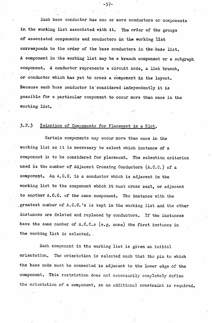
3.2.3 Selection of Components for Placement in a Slot.
Certain components may occur more than once in the
working list so it is necessary to select which instance of a
component is to be considered for placement. The selection criterion
used is the number of Adjacent Crossing Conductors (A.C.c.) of a
component. An A.C.C. is a conductor which is adjacent in the
working list to the component which it must cross next, or adjacent
to another A.C.C. of the same component. The instance with the
greatest number of A.C.C. 's is kept in the working list and the other
instances are deleted and replaced by conductors. If the instances:
have the same number of A.C.C.s (e.g. none) the first instance in
the working list is selected.
Each component in the working list is given an initial
orientation. The orientation is selected such that the pin to which
the base node must be connected is adjacent to the lower edge of the
component. This restriction does not necessarily completely define
the orientation of a component, so an additional constraint is required.
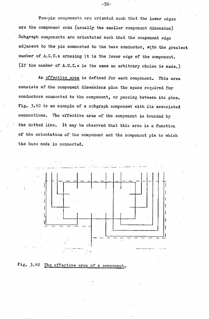
Two-pin components are oriented such that the lower edges
are the component ends (usually the smaller component dimension)
Subgraph components are orientated such that the component edge
adjacent to the pin connected to the base conductor, with the greatest
number of A.C.C.s crossing it is the lower edge of the component.
(If the number of A.C.C.s is the same an arbitrary choice is made.)
- An effective area is defined for each component. This area
consists of the component dimensions plus the space required for
conductors connected to the component, or passing between its pins.
Fig. 3.10 is an example of a subgraph component with its associated
connections. The effective area of the component is bounded by
the dotted line. It may be observed that this area is a function
of the orientation of the component and the component pin to which
the base node is connected..
Fig. 3.10 The effective area of a component...

-59-
The total width r3quired for components and conductors in
the working list is then calculated. There are three possible
relationships between this required width, and the actual slot width
available:-
Required width greater than the slot width.
Obviously not all of the components in the working list
can be placed in the slot. A component with a greater effective
width than another component is given priority of selection.
Thus, the components in the working list with the greatest
effective widths are chosen and the components with the smallest
effective widths are deleted. If there is more than one component
with the same effective width, and it is necessary to make a choice
to avoid the slot width being exceeded, then the components with
the greatest number of A.C.C.s are chosen, and the remaining components
deleted. If no distinction can be made by counting A.C.C.s an
arbitrary choice is made.
Required width equal to the slot width.
In, this case no further selection or orientation is carried
out.
Required width less than the slot width.
To increase the required width to 'fill out' the slot
certain components arm reoriented. Only branch components are
considered for reorientation. Priority is given to components with
the greatest number of A.C.C.s. (The total number of A.C.C.s being
the sum of conductors crossing the component from the left and from
the right with respect to the working list order.) If a component
selected in this way has more A.C.C.s crossing from the left than
from the right it is rotated through ninéy degrees in an
anticlockwise direction. The converse also applies. If the number
of A.C.C.s crossing from left is equal to the number cossing from
the right, then an arbitrary choice of rotation is made.
If all the branch components with A.C.C.s have been
reoriented and the required width is still less than the slot width,
then the reuaining components which do not have any A.C.C.s are
considered for reorientation. In this case branch components with
the greatest effective width are given priority, and the rotation
is chosen arbitrarily.
3.2.4 Placement of Components and Conductor Ends.
At this stage in the Slot Layout procedure it is known
which components and conductors are to be placed and routed in the
slot. Each component has an orientation, an effective area, and
a connected base node. In addition, it may have some A.C.C.s which
must be routed 'through' it. For the purposes of placement the
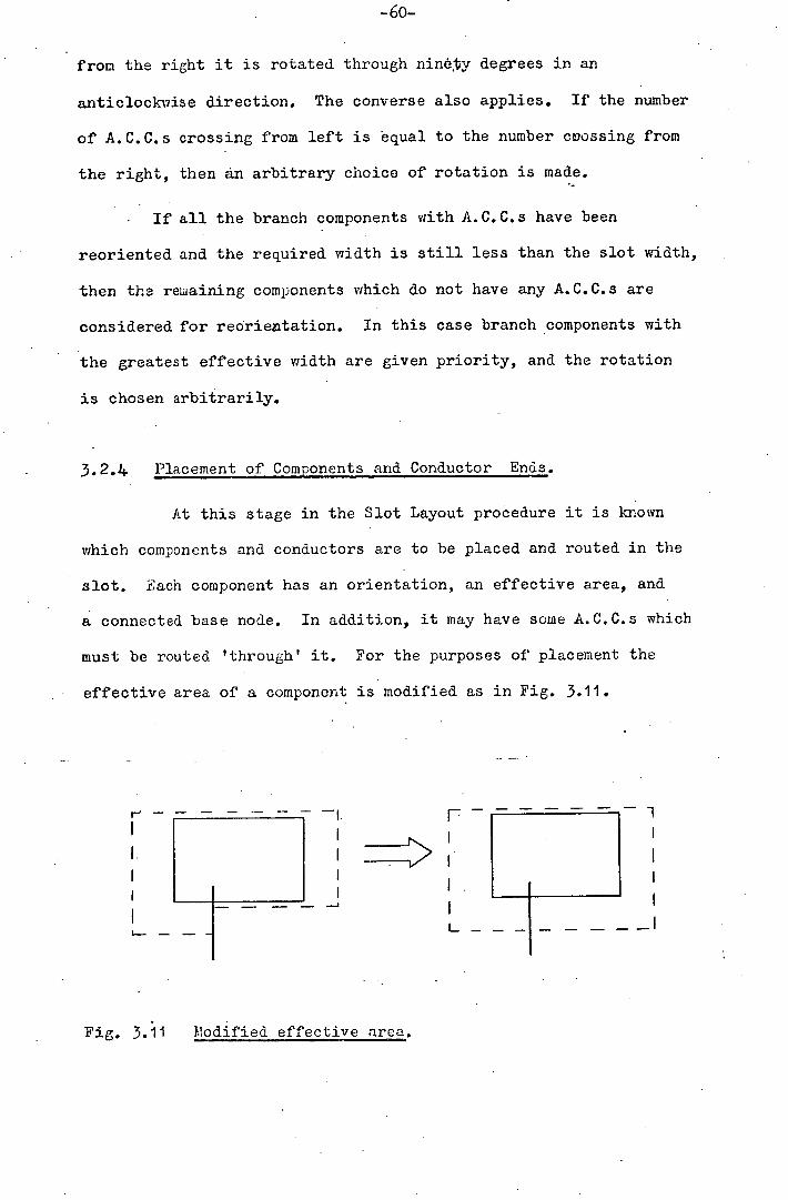
effective area of a component is modified as in Fig. 3.11.
— I
I ]
riH
Fig. 3.11 Modified effective area.

-61- •1 -
Each conductor in the working list is assumed to be a
'conductor end.' with an effective area defined as a square of side
equal to one conductor width. This enables components and
conductors to be placed and routed in a similar way, because, having
positioned the components and conductor ends in the slot, conductors
can then be routed from the base nodes to the conductor ends in the
same way that conductors are routed from the base nodes to the
component pins. To simplify the description of the placement
procedure, components and conductor ends will be grouped under the
general term of 'elements'.
The elements of the working list are positioned as far to
the left of the slot as is possible, without one element sharing
the same x-coordinate as another. Thus, since the effective widths
of all the elements are known, the x-coordinate of each element may
easily be calculated.
The x-coordinate of an element is a function of the
x-coordinates of other elements in the working list. However, the
y-coordinate of an element is calculated independently of the
y-coordinates of other elements. It is necessary to allow sufficient
space beneath an element to allow conductors not connected to it to be
routed without causing track crossings. This is illustrated for a
component element in Fig. 3.12(a). The space required is determined
by first calculating the number of conductors not connected to the
element which need to be routed in the positive x-direction and then
repeating the calculation in the opposite direction.
Starting from the base node to which the element is connected
each adjacent base node is considered in turn, in the required
direction. If the base node is obscured by the element, the element
boundary is extended by one conductor width in the required. direction.

-62-. •1
slol
Base nodes:- 6
5 43 .21 78 9
Element 5432 78
R
31st Base
Base nodes:- 6 5 4 3 2 1 7 8 9
Fig. 3.12 Calculation of-,I-coordinate-of an element.
-63-
The procedure is terminated when a base node is reached which is
not obscured by the element. Base conductors which represent A.C.C.s
in the working list are ignored in the procedure, since allowance
is made for them in the component effective area. Fig, 3.12(b)
shows how the element would be extended for the case in Fig. 3.12(a).
The space required beneath the elements is equal to the
larger of the two element extensions plus one conductor width to
allow space for the base node to which the element is connected.
3.2.5 Conductor Routing.
Each component now has associated with it a position, an
orientation, a base node, and possibly some A.C.C.s. Since the
geometry of a component is known the coordinates of the component
pins may be calculated. Every pin of a component is represented
by a subgraph nob, or by a circuit node, in the graph. By referring
to the mesh, the elements of the graph which connect to, or pass:
between, the pins of a component may be found. Those elements
not connected to the base of the slot must be projected up the board
to form base nodes and conductors of higher slots.
The conductor routing is done in two distinct stages :- -
(i) Component Routing Stage.
The purpose of the Component Routing Stage is to route
conductors away from a component so that they may be projected
upwards or downwards without meeting any obstructions. Fig 3.13(a)
is an example of the way in which conductors associated with
a component are routed. The conductors of the Component Routing
stage for this example are drawn as full lines in Fig. 3.13(b)
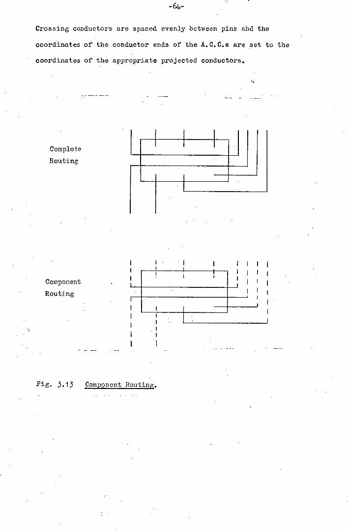
Crossing conductors are spaced evenly between pins aM the
coordinates of the conductor ends of the A.C.C.s are set to the
coordinates of the appropriate projected conductors.
Complete
Routing
Component
Routing
Fig. 3.13 Component Routing.
-65-
(2) Slot Routing Stage.
During this stage conductors are routed from the base nodes
and conductors to the component pins and conductor ends. Two parts
of the same conductor branch or circuit node may occur'-in the base
list. If they are adjacent, then they should be connected in the
slot. If this case occurs the coordinates of the corresponding
conductor ends in the working list are set to the coordinates of
one of the base nodes or conductors. Thus, by routing conductors
from the base nodes (or conductors) to the common conductor end the
required connection is made. Several nested connections of base
elements may be made, providing all the base elements are adjacent
in the base list, and that no conductor is routed around a node to
which further components must be connected.
The basic approach of the routing algorithm is to route a
conductor from a base node, or conductor, in the x-direction until
the x-coordinate of one of the conductor ends to which it must be
connected is reached.. The route is then completed by projecting
the conductor in the y-direction to the y-coordinate of the
conductor end.. Since a simple 'L' shaped conductor routing is
not generally possible without causing conductor crossings each
conductor is routed as far as possible in the required
x-direction, until another conductor is 'hit'. It is then routed
in the positive y-direction by one conductor width. By repeating
this procedure the conductor routing of the slot may be completed.
Fig. 3.14 shows this procedure in operation for a simple
example. Before commencing the procedure proper, each conductor.
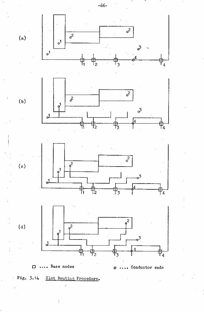
-66-
(a)
(b)
(c)
(d)
Base nodes o Conductor ends
Fig. 3.14 Slot Routinj Procedure.
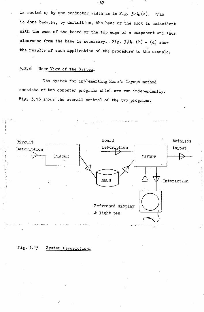
-67—
is routed up by one conductor width as in Fig. 3.14-. (a). This
is clone because, by definition, the base of the slot is coincident
with the base of the board or the top edge of a component and thus
clearance from the base is necessary. Fig. 3.14 (b) - (d) show
the results of each application of the procedure' to the example.
3.2.6 User View of the System.
The system for implementing Rose's layout method
consists of two computer programs which are run independently.
Fig. 3.15 shows the overall control of the two programs.
- Circuit Board
Detailed
Description Descr ion
-1 Layout
PLANAR
LAYOUT
MESH
Interaction
Refreshed display 0 & light pen
Fig. 3.15 Eystem Description.
The PLAIAflProain
The input to this program is adescription of the circuit
and the components used. The description is in the form of a list
Of component geometry definitions followed by a list of. components,
each with associated connections in the circuit. The method, of --
describing the component connections is illustrated in Fig. 3.16
(taken from 1131).
Each component is given a name and the nets of the circuit
are numbered. The names RES, CAP, and TRAN in Fig. 3.16 refer to
component geometry definitions. Thus component Cl is connected to net 6 and edge connector terminal 4, and is of type CAP.
The Output from the program is a data structure which
describes, the mesh of the circuit. This data structure is written
into a file on disc. -
The LAYOUT Pro /
The input to the LAYOUT program consists of a Mesh data
structure plus a board description, and display scale. The board
description is comprised of the board, dimensions, and the
coordinates of the edge connector terminals along the base of the
board.
Facilities exist for manual interaction with the layout.
The layout is displayed on a refreshed display with a light pen
attached. Each component is displayed as a rectangle surrounding
a component name and conductors are represented by line segments
corresponding to the middle of each Conductor track. User
instructions to the program Pre input either by a teletype keyboard
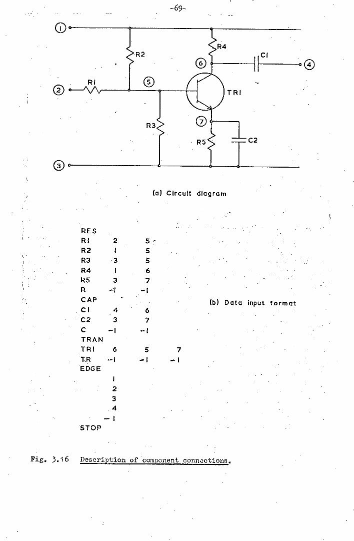
-69- -.
kD
(a) Circuit diagram
RES
Ri 2 5 - . ...
R2 I 5 . .
R3 3 5 ...- -
R4 I 6 .•
R5 3 7 - .. .
CAP . (b) Data input format Cl 4 6
C2 3 7
C -I •-I . TRAN
TRI 6 5 7 .
TR -I
EDGE . . .
2 ..
4 .
STOP
Fig. 3.16 Description of component connections.
-70- I
or by the light pen. Thus, the display transmits input information
to the user.
A number of letters representing the modes of interaction
available to the user are displayed above the top edge of the board.
A particular interaction mode is selected by pointing the light
pen at the appropriate mode letter which doubles in size to indicate
that it has been selected. The functions of the interaction modes
fall into three main groups:-
Mode selection and implementation.
An interaction mode is not implemented until a confirmation
mode, M, (for 'Modify') is selected. This is provided to give the
user a safeguard against errors in selection.
When the program is waiting for the next interaction it is
automatically set to a mode called Reset mode (R). This mode may
be selected to instruct the program to disregard another
interaction instruction which has been partially set up.
Control of the automatic layout process;.
The user may instruct the program to automatically layout
the next slot, or to complete the rest of the layout by selecting
Unchange rnode(U), or Express mode (x), respectively. Another mode
called Finish mode (F) is used to terminate the program run.
1odifications to the layout form.
The layout is modified by altering the selection of
components for slots, or by changing component orientations. To.
set up a particular modification, an interaction mode is selected
and then the component to which it is to be applied is identified.

Then the the modification is implemented the contents of all slots above
the slot containing the selected component are deleted. This is
necessary because of the method of 1aut construction. Three
interaction modes are available within this group,
Delete Mode - D.
The selected component is removed from the slot, and is
eventually placed in a higher slot. The resulting space is
automatically filled by inserting another component which could
have been placed in the slot, or by reorienting components already
placed in the slot.
Pull Mode - P.
This mode allows the user to 'pull' the selected component
out of the slot in which it is placed into a lower slot in which
it could have been placed. The lower slot, is selected by allowing
the user to move the component outline across the display screen
with the light pen until it is in the required. slot. The user has
no control over the position of the component in the new slot,
since this is predetermined by the order of the base nodes and
conductors of the slot. Components are automatically deletpd in
order to make room for the new component using the criteria
described in Section 3.2.3.
Orient Mode— 0.
A marker is displayed on the selected component to
indicate its orientation. This marker is then rotated through
ninety degree steps in a clockwise, or anticlockwise direction,
depending on whether the user types in a 'C' or an 'A' on the
teletype keyboard. The component may only be given an orientation

- 72-
in which the pin to which its base node is connected is adjacent
to the lower edge of the component, as described in Section 3.2.3.
If there is insufficient space in the slot for the
component to be reoriented an error message is output to the
teletype and no action is taken.

-73-
Chapter 4. Requirements of a System for the Design of Printed Circuits.
The purpose of this chapter is to formulate the general
requirements of a system for the design of printed circuit board
layouts.
41 Constraints on Layout Desi gn .
There are many constraints which must be satisfied when
designing a layout. Some are obvious, such as the constraint that
the layout represent-the circuit, and that tracks do not cross.
Others are not so obvious, and vary with the application and the
particular industrial environment. The most common of these
constraints will now be described.
4.1.1 Component Packing Density.
The range of application of a design system is dependent
on the packing densities which may be achieved using it. Thus, it
may not be possible to layout a particular circuit if the packing
density required is higher than the system can achieve. In addition,
it is generally desirable to have a certain amount of board space
(usually about Ic of the board area) so that components may be
added in subsequent modifications.
The layout problem becomes more difficult to solve, and
consequently more time consuming, with increasing packing densities.
It may be deduced from the above that packing density is
an important factor when estimating the potential usefulness of a
computer system for layout design.

- 74-
4.1.2 Electrical Constraints.
In certain types of circuits undesirable coupling of
energy between signal paths may occur in the layout. To avoid this
effect conductors are usually kept as short as possible, and as far
apart as. possible.
Another adverse effect on circuit performance may occur if
a 'noisy' component is placed near to other components susceptible
to picking up noise. To reduce this effect such components are
usually kept as far apart as possible in the layout.
4.1.3 Mechanical Constraints.
Printed circuit boards come in many different shapes and
sizes. In addition, it may not be possible to use all of the board
area for layout, if certain areas are allocated for other purposes.
Though printed circuit bards usually have only one edge
connector, many boards require two or more.
In some applications, the vibration characteristics of a
board are important. In such cases it is necessary to ensure that
heavy components are not grouped together away from the board
supports.
4.1.4 Thermal Constraints.
When deciding on the width of a particular conductor track
it is necessary to consider not only the manufacturing constraints,
but also the temperature rise induced by the current passing through
it, since overheating may cause track failure.
-75-
During component placement it is necessary to consider the
power being dissipated by components to ensure that maximum
component operating temperatures are not exceeded e.g. components
generating 1 Watt or more must, in general, be placed near to a heat
sink to prevent overheating.
4- 11 .5 Manufacturing Constraints.
Track widths are limited not only by thermal constraints,
as described above, but also by manufacturing constraints. Below
a certain width, depending on the manufacturing process used, the
loss of definition inherent in photographic etching results in
uneconomic yields.
Another constraint which directly effects the printed circuit
layout design is the standardisation of component layout. The fixing
of component lead pitches, and component orientations, to a standard
pattern greatly facilitates the assembly of boards, and enables
automatic or semi-automatic machines to be used.
4.2 The Need for Interaction.
Ideally, a general system for designing printed circuit
board layouts should be completely automatic. The circuit definition
and the constraints would be fed into the system, and a complete
layout design, which satisfies. all the constraints, produced. It
is the author's opinion that to expect such a system within the limits
of current printed circuit board technology is unrealistic.
The system would necessarily incorporate constraints such
as those described in the previous section. Some of these constraints

- (.b-
are not well defined e.g. to avoid cross-coupling effects
between signal lines it is desirable to keep the corresponding
conductor tracks short and as far - apart as possible. How short must
the conductors be to avoid the effect? How far apart is far enough?
Is it necessary to completely avoid the effect, or merely to reduce
it below an acceptable level for a particular pair of lines? It is
extremely difficult to completely specify all the parameters
necessary to automatically impose such a constraint on the layout
design process.
The constraints are not - in general complimentary e.g. it
may not be possible to obtain the required packing density without
partially relaxing thermal, or vibrational constraints. Thus, it
is necessary to take the relative importance of the constraints
into consideration within the system.
Even if the system is able to incorporate all the constraints
and their relative importance, there is still no guarantee that a
solution will exist for a particular problem. In manual systems
changes are made to the data, components may be allocated to
other boards, or be replaced by components with more suitable
characteristics. It is extremely doubtful whether an automatic
system could carry out these type of functions.
The probability is that a large burden would be placed on
the circuit designer. He would be required to supply not only the
circuit diagram, but also a large amount of information relating
to the circuit, and board data. He would need to specify the
relative importance of the constraints, and their acceptable levels.
In order to prepare this information, the circuit designer would,

- 7.7-
in all probability, need to refer to some form of layout realisation.
Indeed, it is not unlikely that the circuit designer would have to
design the layout himself in order to provide all the required
information.
It may be deduced from the above discussion that, at the
present time, the man plays an essential part in any printed
circuit board layout design process.
It is argued-that an automatic system may be used to
produce a layout, or part layout, which goes some way towards
satisfying all the constraints. This layout can then be modified
by hand to obtain a final design which does satisfy all the constraints.
The problem with this approach is that the final design is not stored
in the computer. One of the main advantages of using a computer
based design system is that layouts, artworks, and drilling tapes
can be produced automatically, and to the required accuracy
directly from the final layout stored in the computer. It is
necessary to have this advantage to offset the cost of data preparation.
If the part layout is manually modified it is necessary to go through
an additional data preparation phase - usually digitising - to get
the design back into the computer.
The best approach would appear to be to modify the layout
design stored in the computer using manual interaction.

4.3. Interaction Requirements.
When designing a system of interaction it is necessary
to consider certain requirements. These requirements may be
separated into communication requirements and functional requirements.
The latter refers to what the user is able to do using the system,
and the former to the way in which he is able to do it. These two
categories of requirements will now be discussed.
4.3.1 Communication Requirements.
The design process is essentially an iterative procedure
in which the final design is reached by evaluating and modifying
intermediate designs. In an interactive design system, modifications
to the design stored in the computer are made using the interaction
facilities, and information on intermediate designs is fed back to
he user for evaluation. This feedback of design information
should be in the form most natural for tue user to comprehend. Thus,
in layout design, the feedback should be in the form of pictures of
the layout or part of the layout.
In order to communicate with the computer, the user requires
some form of language. The most important requirements are that
the language;
(i) Should be related to the design problem, and not the
computing environment, and thus require no computing
expertise. on the part of the user,
should be concise,
should be simple to use,

-79:-
(14.) should allow the user to express. himself naturally.
The language need not be restricted to combinations of words.
The most natural way for the user to identify a part of a layout
which he wishes; to modify, is to point at it in the picture displayed
by the computer. Indeed, such an identification pracedure; would
seem to- satisfy all the language requirements listed above. However,
operations on the layouts are most naturally described using
combinations, of symbols. and/or words. Thus, a language consisting
of a combination of actions on the pictures, and words; or symbols
is required.
There are other requirements which derive from ergonomic
considerations. One such consideration is the respons;e of the
interaction system. In a conversation between two. people it
becomes frustrating if there are pauses; of greater than
approximately two seconds. [15] The same applies to a conversation
between user and computer. In general, the patience of the user in
waiting for results is dependent on the size and complexity of the
operations: the computer is being asked to perform. Thus, the user
might become extremely frustrated if he has: to wait five seconds for
a trivial acknowledgement of a request, and yet be quite prepared
to wait twenty seconds for the results of an extensive design
modification.
Another consideration is the devices used to communicate
with the computer. Ideally, all communications: should be made using
the same device, to avoid the need to swap from one to another
when making modifications The most suitable devices for interactive
layout design are graphic displays. These devices enable fast feedback
IM
of design information, and part of the screen may be used for
language words or symbols, which may be selected with a light pen
or cursor. Thus, a single device may serve as the communication
medium for the interactive system.
1.3.2 Functional Requirements. .,
A design is achieved by satisfying a number of design
constraints. It is convenient to group these constraints into two
categories,
(i) Global constraints: are those constraints not dependent
on a particular set of design data, e.g. 'the layout must
represent the circuit.'
(2) Data constraints are those constraints dependent on a
particular set of design data, e.g. consideration of
cross-coupling effects and thermal characteristics.
Ideally, the interaction facilities should allow the user
to make any modifications to the design which satisfy the global
constraints. Thus, the user should be protected from making any
modification which would automatically invalidate the design.
In layout design the basic functional requirements:. for interaction
are that the user be able to place a component anywhere on the board,
at any orientation, and route. conductors in any valid manner between
the components. In addition to these basic requirements, there is
a requirement for other facilities which help the user to satisfy
the data constraints, e.g. the grouping of selected components, the
calculation of thermal and vibrational characteristics etc.

-81-
An additional requirement to the above is that the user be
able to store, and subsequently reinstate, intermediate.d.es±gns,
This is desirable because the user may wish to go back to a particular
intermediate design having discovered the more recent modifications-
have not led to any improvement in the layout design.

Chapter 5. 5. Evaluation of Rose's Design System.
The purpose of this chapter is to evaluate the performance
of Rose's system in relation to the requirements formulated. in
Chapter 4. It is perhaps worth noting that the criticisms of Rose's
system contained in this chapter have been made with the considerable
aid of hindsight.
5,1 Automatic Layout Capabil ity.
The automatic parts of the system partially satisfy the
requirements relating to global constraints.
Automatic layouts of three circuits termed A,B,and C are
shown in Figs 5.1, - 5.2, and 5.3. These examples show that the
system produces layouts with very poor packing densities and very
long conductors. In addition, the system does not satisfy the
requirements for catering for boards other than rectangular in shape,
nor does it allow more than a single edge connector to be used.
Only one width of conductor track may be used in any particulat layout.
It may be observed in the examples that there are no component
overlaps, and the conductors are routed correctly between component
pins. However, when larger circuits with a greater number of
components with more than two pins, were used, the following problems
occurred,
(i) conductor conflicts within component areas for components
with more than two pins,
(2) if conductors were rejected at the PLANAR stage, no account
was taken in LAYOUT of the fact that some component pins

-83-
LL
ri
Fig. 5.1 Automatic layout of circuit A.
0
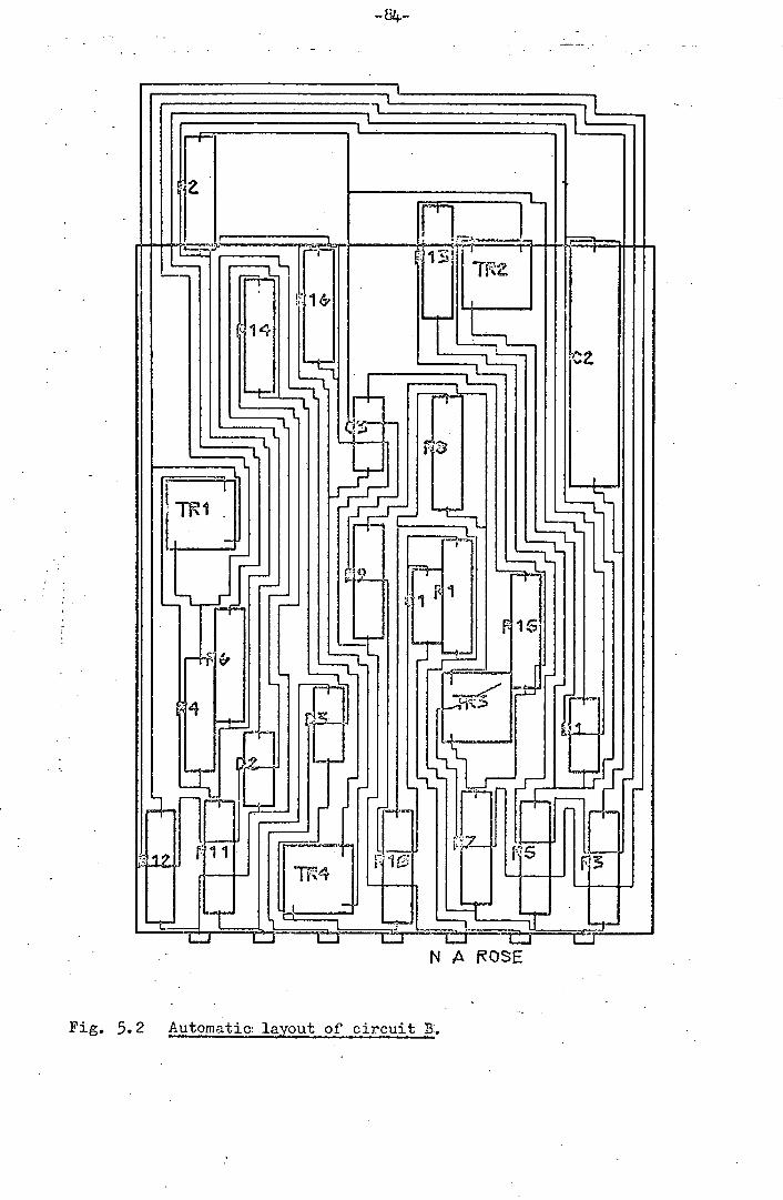
-64-
N tb. ROSE
Fig. 5.2 Automatic layout of circuit B.
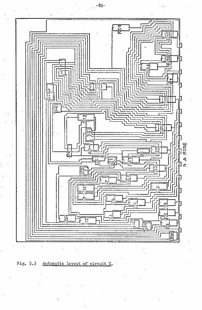
ILL
0
H
rd VA
Fig. 5.3 Automatic layout of circuit C.
IM
did not require connections to be made to them, and illegal
connections resulted.
The net effect of both (1) and (2) was to cause the system
to fail due to the LAYOUT program entering an 'infinite loop'.
This did not occur for circuits A, B Y and C because they were small
and no conductors were rejected at the PLANAR stage.
The automatic layout capability is a function of the number
of crossings. in the mesh as a proportion of the number of componeiits
in the circuit. This is clearly illustrated by comparing the layout
of circuit A (Fig. 5.1 ) with the layout of Circuit C (Fig. 5.3)
The PLANAR program is rather inefficient at limiting the
number of crossings. This is clearly illustrated by the example
circuit in Fig. 5.4 (a) which is obviously planar. The data was
organised such that no conductors could pass. between component pins.
The PLANAR program produced the mesh drawn in Fig. 5.4 (b) leaving
out component 6 which would otherwise have been inserted by using
a crossing conductor.
When determining the number of conductors which may pass;
between component pins;, the component pads are all assumed to be
of the same width as the conductors. Usually pads have a greater
width than the conductors;, and thus the assumption is. false, and
would lead to conductor/pad conflicts when laying out practical
circuits.
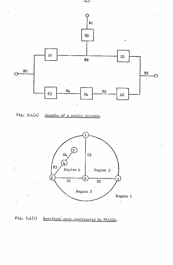
- b7-
Fig. 5.4(a) ixarnp1eof a sirriDle circuit.
Cl/ JC5
C31/ Region 4 J Region 3
Cl C2
Region 2 Region l
Fig. 5.4(b) Constructed by PL/I'
5.2 Interaction Capability.
It was neither possible nor desirable to use interaction
to compensate for the shortcomings of the program in satisfying the
global constraints.
Figs 5.5, 5.6, and 5.7 show that substantial improvements
in packing density are obtainable using interaction, though the
results are still very poor when compared with manual layouts.
A limited amount of control is given over component
positions. and orientations, allowing partial satisfaction of other
data constraints e.g. the separation of 'hot' components into
separate slots, the reduction of critical conductor lengths etc.
Hawever, the control is considered to be very inadequate in relation
to the system requirements. In addition, no facility exists for
storing and reinstating layouts, or part layouts.
5.3 Computational Efficiency.
Rose implemented his system on an Elliot 4130 computer
linked to a satellite PDP-7 with 340 display. The author
transfered the system to a DEC PDP-1 0. linked to a FDP-7 with 340
display. Though written in FORTRAN the system was not found to be
easily transferable, due to incompatabilities. in the FORTRAN compilers
for the two machines.
Due to a lack of foresight on the part of the author, the
execution times required to produce the layouts of A, B, and C
circuits. were not tabulated for the first working version of the
system on the PDP-10. As a result of changes in the computing
system, difficulties arose in obtaining these execution times at the

Ui
0
Fig. 5.5 Layout of circuit A modified by interaction.
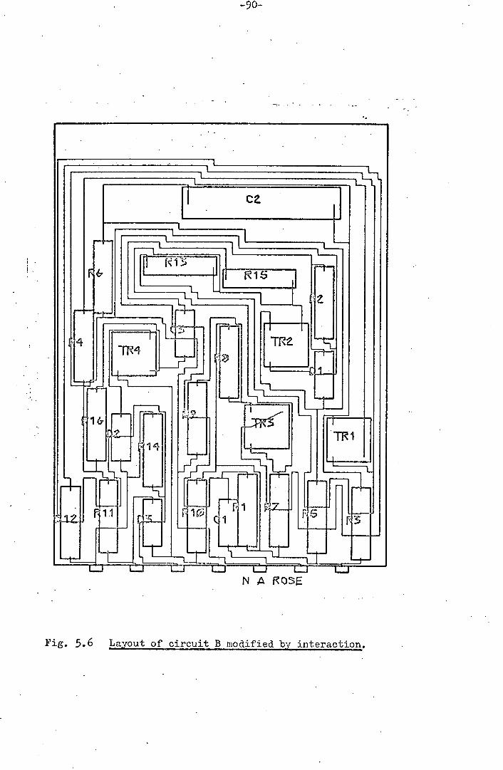
-90-
4 Hft1:rI1 L
TR
L
mczHi[
Fig. 5.6 Layout of circuit B modified by interaction.
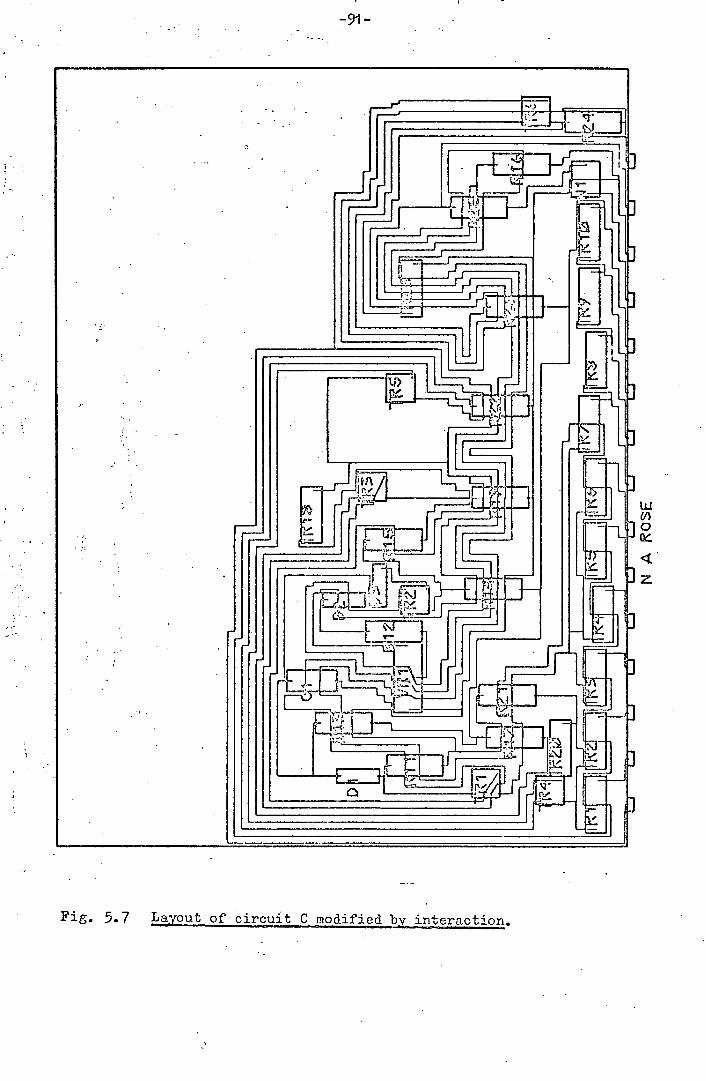
-91-
• -J
1 J-LJ
• _
Lu 01 0
1-F:
Fig. 5.7 yutof 'circuit C modified byinteraction.

-92-
time of publication for this version. Because there was no facility
for measuring execution time on the ifl3O, Rose's times were obtained
using a stop watch, and are therefore rather approximate. This
method was found to be impractical for estimating execution times
for the interactive runs.
The execution times and storage requirements of the PLANAR
and LAYOUT programs are shown in Fig. 5.8. For compatability with
later implementations of the LAYOUT program on the PDP-1 0 the
LAYOUT execution times obtained on the 4130 have been factored by
0.3 which approximately represents the difference in execution
speed of the two machines. The times quoted for the PLANAR program
were obtained on the PDP-10.
Though approximate, the execution times indicate that the
system is very fast. This is partially attributable to the fact
that virtually no packing of data into words is used. Aa a result,
the data storage space required tends to be rather large. This was
found to be a limiting factor when the system was used on larger,
more realistic circuits.
The interaction system is rather inefficient with respect
to execution time. Each time an interaction is implemented all of
the layout up to the slot containing the component to be modified
is regenerated, even though the positions and the orientations
of the components are known. This-regeneration dncludes the
rebuilding of the picture. The inefficiency of this approach becomes
more apparent when one considers that very often it is desirable
to make a series of modifications to components in the same slot.
It was found to bc impossible to run realistic circuit

-93-
layout problems on the system because of the large number of logical
errors in the program. The LAYOUT program was virtually untested
for sub-graph. components with more than 3-pins, and as a result
fatal errors occured in the majority of cases in which they were
tried.
5,4 Interaction Efficiency.
The interaction facilities were found to be inadequate,
difficult to use effectively, and prone to error.
When a component is deleted from a slot, the resulting
space is automatically filled, either by inserting an unpiaced
component, or by reorientating existing components. Thus, if
the user wants to reduce the number of other components in.. a slot
it is necessary, in general, to delete other components which are
automatically inserted into the slot.
In order to change the orientations of a component it is
necessary to create enough space for a new orientation by going
through the deleting process.
The PULL mode of interaction is very difficult to use,
and very prone to error in which the program goes into an
infinite loop state.
There is no facility to enable a component's position to
be fixed within a slot. Thus, if two components: are adjacent in
a slot it is not possible to move them apart to reduce adverse
electrical effects unless one of them is deleted from the slot.
Because no facility exists for storing and reinstating
layouts a great burden is placed on the user to remember a
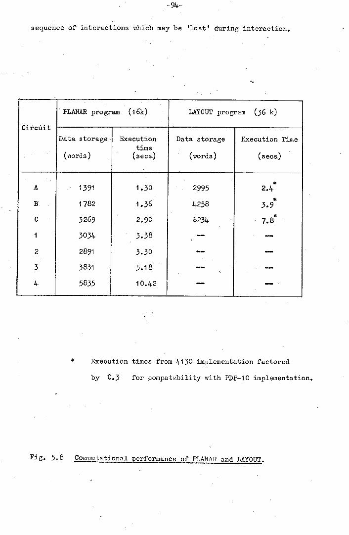
sequence of interactions which may be 'lost' during interaction.
Circiuit
- PLANAR program (16k) LAYOUT program (36 k)
Data storage. Execution Data storage Execution Time time
• (words) . (sees;) (words.) (sees)
A . . 1391 1.30 2995 *
2.4
B . 1782 1.36 1258 3.9
C 3269 2.90 8234 . 7.8
I 3034 3.38 - . _
2 2891 3.30
3 3831 5.18
5835 10.2 -
* Execution times from 4130 implementation factored
by 0.3 for compatability with PD?-10 implementation.
Fig. 5.8 Computational ierformance of PLANAR and LAYOUT.
-95-
Chapter 6 Component Selection and Placement.
The most important phase of the LAYOUT program is the
selection and placement of components in slots. It is this phase
that determines the form of the layout.
The algorithms for selecting and placing components have been
rewritten.
In this chapter the new approach to component selection
and placement is discussed in relation to, what are considered to be
the weaknesses of Rose's method, and the new method of component
selection and placement is described..
6.1 The Problem.
The Working List of a slot contains the components and
conductors which may be placed and defines the order of placement.
The Working List: is obtained by developing the nodes and conductors
of the Base List and the slot geometry is determined by the placement
of components in lower slots.
The Working List, the Base List and the slot dimensions
together provide most of the information required by the component
selection and placement algorithm.
The most important constraints on component selection and
placement are the form of the mesh, manifest in the ordering of
components and conductors in the Working List, and the slot dimensions.
Because of the constraint of the mesh, the selection and
placement of components for a slot largely determines the conductor
routing, and consequently largely determines the layout of the slot.
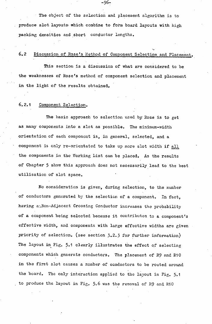
The object of the selection and placement algorithm is to
produce slot. layouts which combine to form board layouts with high
packing densities and short conductor lengths.
6.2 Discussion of Rose's Method of Component Selection and Placement.
This section is a discussion of what are considered to be
the weaknesses of Rose's method of component selection and placement
in the light of the results obtained.
6.2.1 Component Selection.
The basic approach to selection used brRoae is to get
as many components into a slot as possible. The minimum-width
orientation of each component is, in general, selected, and a
component is only re-orientated to take up more slot width if all
the components in the Working List can be placed. As the results
of Chapter 5 show this approach does not necessarily lead to the best
utilisation of slot space.
No consideration is given, during selection, to the number
of conductors generated by the selection of a component. In fact,
having a..---..Non-Adjacent Crossing Conductor increases the probability
of a component being selected because it contributes to a component's
effective width, and components with large effective widths are given
priority of selection. (see section 3.2.3 for further information)
The layout in Fig. 5.1 clearly illustrates the effect of selecting
components which generate conductors. The placement of R9 and RIO
in the first slot causes a number of conductors to be routed around
the board. The only interaction applied to the layout in Fig. 5.1
to produce the layout in Fig. 5.6 was the removal of R9 and RIO
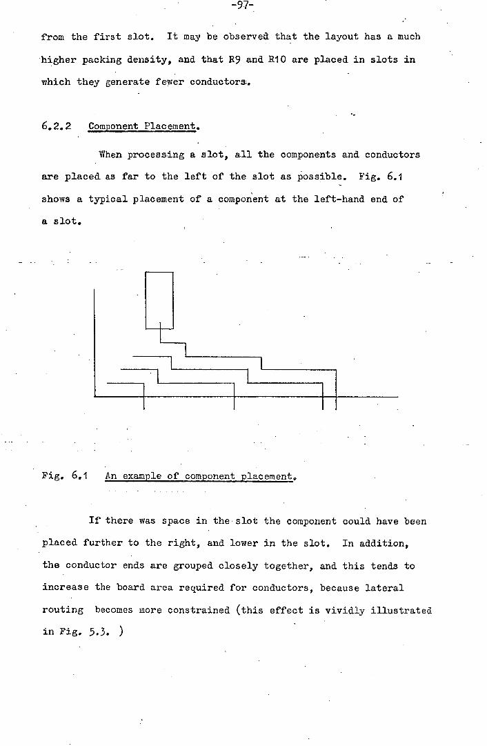
-97-
from the first slot. It may be observed that the layout has a much
higher packing density, and that R9 and R10 are placed in slots in
which they generate fewer conductors.
6.2.2 Component Placement.
When processing a slot, all the components and conductors
are placed as far to the left of the slot as possible. Fig. 6.1
shows a typical placement of a component at the left-hand end of
a slot.
Fig. 6.1 An example of component placement.
If there was space in the slot the component could have been
placed further to the right, and lower in the slot. In addition,
the conductor ends are grouped closely together, and this tends to
increase the board area required for conductors, because lateral
routing becomes more constrained (this effect is vividly illustrated
in Fig. 5.3. )
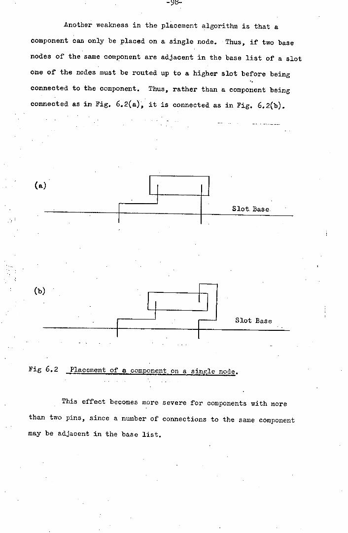
Another weakness in the placement algorithm is that a
component can only be placed on a single node. Thus, if two base
nodes of the same component are adjacent in the base list of a slot
one of the nodes must be routed up to a higher slot before being
connected to the component. Thus, rather than a component being
connected as in Fig. 6.2(a), it is connected as in Fig. 6.2(b).
(a)
Slot Base.
p -
Slot Base
Fig 6.2 Placement of a component ona single node.
This effect becomes more severe for components with more
than two pins, since a number of connections to the same component
may be adjacent in the base list.
-9.9- I
6.203 Component Representations.
A component is represented by a rectangle which contains
the component body and the pads. Only conductors which connect to,
or cross, a component may be routed inside this area.. This places
an artifical constraint on the conductor routing, since conductors
need only be routed around component pads, and not the component
bodies. This constraint results in longer conductors, and lower
packing densities than are actually necessary.
6.2.4 Placement of Conductor Ends.
Conductor ends are placed in the same manner as components.
They are placed as far towards the left of the slot as possible,
except for those between the right-most placed component and the
slot edge. In this case, the conductor ends are positioned with
the same x-coordinates as the base nodes. Fig 6.3(a) shows the
way in which conductor ends would be placed without this exception s -
Fig. 6.3(b) shows the way in which they are placed.
As described in Section 3.2.5 conductors or nodes in the
Base List may be connected together if they are part of the same
circuit node or conductor branch, and adjacent in the Base List.
However, this situation is not detected until the conductor
routing stage, and subsequent to the selection and placement of
components and the placement of conductore.n;. If two nodes
or conductors are connected together in a slot they require less
space, and there is no requirement for them to be routed up to
higher slots.
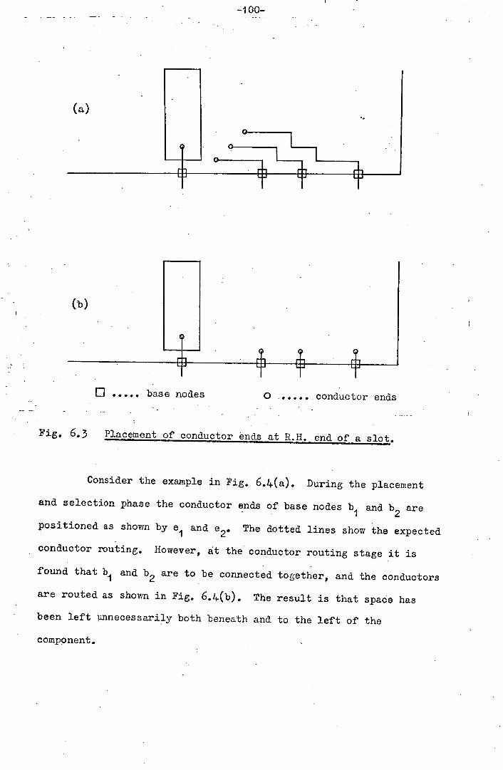
-100-
0 ..... base nodes 0 .......conductor ends
Fig. 6.3 Placement of conductor ends at R.H. end of a slot.
Consider the example in Fig. 6 .4(a). During the placement
and selection phase the conductor ends of base nodes b 1 and b2 are
positioned as shown by e 1 and e 2. The dotted lines show the expected
conductor routing. However, at the conductor routing stage it is
found that b1 and b2 are to be connected together, and the conductors
are routed as shown in Fig. 6.4(b). The result is that space has
been left Pnnecessarily both beneath and to the left of the
component.

101
(a)
Pb3
Fig. 6.4 Effect of connected base nodes on component placement,
6.3 The New Ap2roach to Component Selection and Placememt.
The main objectives of the new approach are to improve
the utilisation of slot space, and to control the number of conductors.
generated. This section is a discussion of the implications of
these objectives.

-102-
6.3.1 Slot Packing Density.
The, area of a slot is considered to be defined by the base
and sides of the slot, and the tops of placed components as in the
example in Fig. 6.5.
Fig.6.5 Slot area.
The packing density, Ds,.of a slot is given by,
Ds = Area of components
Slot area
1,; 4e cking densities be achieved? The question arises-- how can 4 a
Component areas can be calculated quite easily, for any component
selection, from component geometries. However, slot area is dependent
on component positions and orientations. Consequently it is
necessary to place components in a slot to determine the slot area.
It is not possible to predict - which particular selection
of components will give the highest value of Ds, when placed,
therefore it is necessary to place a number of component selections

-103-
i.e. to perform Trial -Placements of components in the Working List.
In order to find the component selection with the highest value of
Ds, every combination of components in the Working List must be placed.
If there are n components in the Working List the total number of
combinations to be placed is given by,
• To = 2' - I (ignoring the null
• combination)
If there. are 10 components in the Working List (a typical
number) then the number of combinations is 1023. This is a large
number of Trial Placemzents to perform for the interactive operation
of the LAYOUT program to be retained. In addition, a component can
be placed at a maximum of three orientations, and each component
orientation requires independent consideration. For the above
example this would mean over a' million Trial Placements. would need
to be performed. It may be concluded that it is essential that the
method of Trial Placement be as efficient as possible, and that the
number of Trial Placements be kept to a minimum.
6.3.2 Conductor Generation.
In Section 6.2.1 it was shown that the generation of
conductors in a slot can have' an adverse effect on the layout of
subsequent slots. It is,,therefore, desirable to make component
selection a function of conductor generation as well as of
component packing density. However, to do this it is necessary to
clarify what is meant by 'conductor generation', and to define some
quantative measure of it.
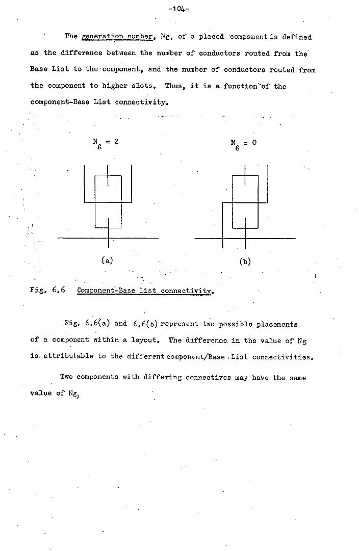
-104-
The generation number, Ng, of a placed component is defined
as the difference between the number of conductors routed from the
Base List to the-co mponent, and the number of conductors routed from
the component to higher slots. Thus, it is :a function' -of the
component-Base List connectivity.
N = 2 C
N = 0 C
(a) (b)
Fig. 6.6Component_-Base List connectivity.
Fig. 6.6(a) and 6.6(b) represent two possible placements
of a component within a layout. The difference. in the value of Ng
is. attributable to the different component/Base List connectivities.
Two components with differing connectives may have the same
value of Ng)
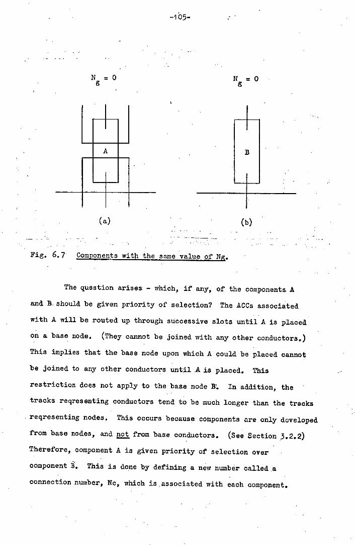
-105-
N =0 g N = 0
g
LI
(a) (b)
Fig. 6.7 Components with the same value -o- Ng.
The question arises -..- which, if any, of the components. A
and B. should be given priority of selection? The ACCs associated
with A will be routed up through successive slots until A is placed
on a base node. (They cannot be joined with any other conductors.,)
This implies that the base node upon which A could be placed cannot
be joined to any other conductors until A is placed. This
restriction does not apply to the baste node B'. In addition, the
tracks reqresenting conductors tend to be much longer than the tracks
reqresenting nodes. This occurs because components are only developed
from base nodes, and not from base conductors. (See Section 3.2.2)
Therefore, component A is given priority of selection over
component B. This is done by defining a new number called .a
connection number, Nc, which is associated with each component.
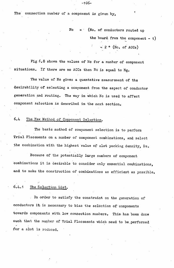
-i06-
The connection number of a component is given by,
No = (No. of conductors routed up
the board from the component - 1)
- 2 (No. of ACCs)
Fig E.8 shows the values of No for a number of component
situations. If there are no ACCs then No is equal to Ng.
The value of No gives a quantative measurement of the
desirability of selecting a component from the aspect of conductor
generation and routing. The way in which No is used to affect
component selection is described in the next section.
6.4 The New Method of Component Selection.
The basic method of component selection is to perform
Trial Placements on a number of component combinations, and select
the combination with the highest value of slot packing density, Ds.
Because of the potentially large numbers of component
combinations it is desirable to consider only essential combinations,
and to make the construction of combinations as efficient as possible.
6.4.1 The Selection List.
In order to satisfy the constraint on the generation of
conductors it is necessary to bias the selection of components
towards components with low connection numbers. This has been done
such that the number of Trial Placements which need to be -.performed
for a slot is reduced.
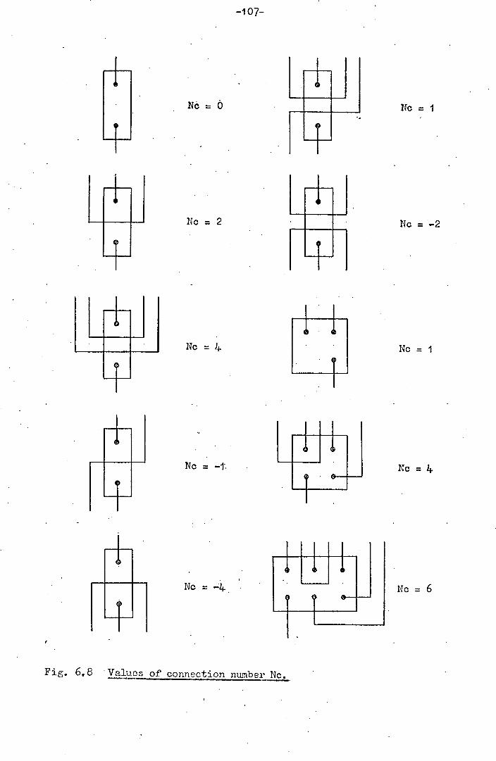
-107-
No = O No = I
Nc = 2
No = -2
No = 1+ No = I
Nc = Nc =
Nc=-24. Nc = 6
Fig. 6.8 Values of connection number Nc.

Initially, the the set of components with the lowest connection
number is extracted from the slot Working List to form another list
called the Selection List. Trial Plaôëments are then performed on
combinations of the components in the Selection List. The
component combination with the highest packing density is placed
in the slot, and those components in the Selection List which have
not been selected are deleted. A new Selection List is then
constructed from the remaining components in the Working List.
Trial Placements are then performed on the placed components plus
combinations of components in the Selection List. This process is
illustrated in Fig. 6.9. It tends to drastically reduce the number
of Trial Placements to be performed, e.g. if the were eight components
in the Working List of a slot and all the components were in the
Selection List at once, and each component could be placed at one
of three orientations, then the total number of possible combinations
would be 65,535. However, if the first Selection List contained
Jf components, the second contained 3 components, and the third
contained 2 components, then the total number of possible
combinations would be 335. -
As the process proceeds there is, in general, less-and less
space in which to place the components in sucessive Selection Lists.
This tends to reduce the number of combinations further, because
Trial Placements are not performed on combinations which require.
more than the available slot width. (See Section 6.4.2) However,
a. situation could arise in which all the components could be placed
and produce the slot layout with the highest packing density. In
such a case the component connectirities would affect the order of
component selection and placement, but would not prevent components
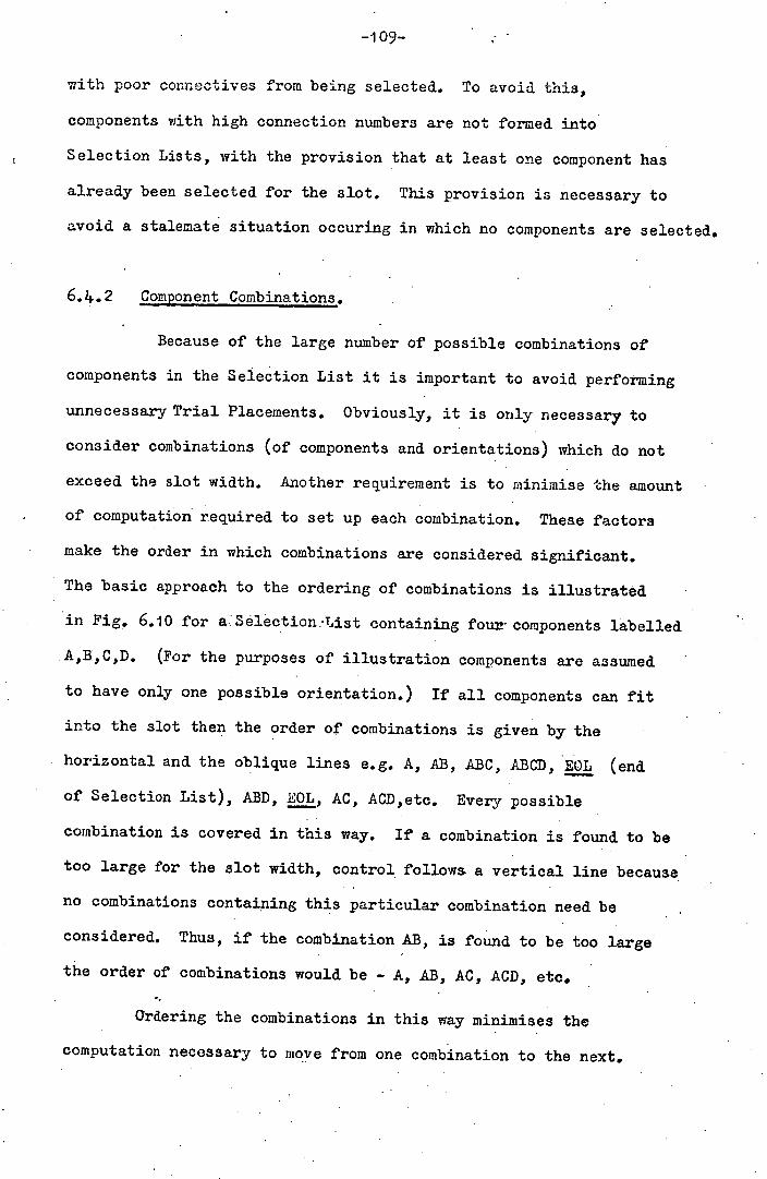
-109--
with poor connectives from being selected. To avoid this,
components with high connection numbers are not formed into
Selection Lists, with the provision that at least one component has
already been selected for the slot. This provision is necessary to
avoid a stalemate situation occuring in which no components are selected.
6...2 Component Combinations.
Because of the large number of possible combinations of
components in the Selection List it is important to avoid performing
unnecessary Trial Placements. Obviously, it is only necessary to
consider combinations (of components and orientations) which do not
exceed the slot width. Another requirement is to minimise the amount
of computation required to set up each combination. These factors
make the order in which combinations are considered significant.
The basic approach to the ordering of combinations is illustrated.
in Fig. 6.10 for a.Selection:Tjist containing four- components labelled
A,B,C,D. (For the purposes of illustration components are assumed
to have only one possible orientation.) If all components can fit
into the slot then the order of combinations is given by the
horizontal and the oblique lines e.g. A, AB, ABC, ABCD, EOL (end.
of Selection List), ABD, EOL, AC, ACD,etc. Every possible
combination is covered in this way. If a combination is found to be
too large for the slot width, control follows a vertical line because
no combinations containing this particular combination need be
considered. Thus, if the combination AB, is found to be too large
the order of combinations would be - A, AB, AC, ACD, etc.
Ordering the combinations in this way minimises the
computation necessary to move from one combination to the next.
-110-
Begin
Construct a Selection List
\ /E~ Have all the components in the W.L. been considered ? )
NV
Perform Trial Placements on combinations of the Selection List + components aliready placed.
Place the components in tbe best combination and delete the other components in the Selection List.
Place conductors ,Develop components.
End
Fig. 6.9 Effect of Selection List on Component Selection .
-Ill.-
A .ABCD
D
Fig. 6.10 Ordering of Component Combinations.
Perform Trial Placement
The combination is too
big for the slot.
End of the Selection
List.

-11.2-
E.g. after a Trial Placement has been performed on the combination
AC the next combination is obtained merely by either adding D or
by removing C and adding D.
The approach described above must be extended to account
for component orientations. One method of doing this would be to
consider all the combinations of orientations for each component
combination. However, this would not allow component combinations
which are too large to be avoided by the method described above,
because for the same component combination, some combinations of
orienatations may be too large for a slot, whilst others may not.
Thus, all the component combinations would have to be considered.
The actual method which is used allows the reduction of the number
of combinations in the same manner as described above. In Fig. 6.11
the order of combinations, including orientations, is given for three
components labelled A,B, and C. Each component is assumed to have
two possible orientations, indicated by the suffices. *
6.5 Method of Trial Placement.
This section is a description of the way in which a
Trial Placement is. performed.
6.1.1 Component Representations.
The method of component representation has been modified
such that each component has a pad diameter associated with it.
(In Rose's system every component is automatically assigned pads
with diameters equal to the conductor width). As shown in Fig. 6.12
each component is represented by two areas.
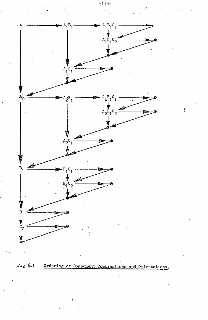
-113-
A.B A1B1.C1
AB1 We. A2131 .C 1
B1 ,'. B1 C 1
Fig 6.11 Ordering of Component Combinations and Orientations.
-llii.--
(a) Component Placement Area
1..
(b) Component Routing Area
Fig. 6.12 New component description.
The component placement area is a rectangle containing, all
the pads and the component body. It represents the area required
by a component on the 'component-side' of' - the board. The component
routing area is a rectangle which contains all the pads of a
component. It represents the area required by a component on the
'routing side' of the board. The positions and the size of the pads
of a component determine the number of conductors which may be
routed between the component pins. The effective area of a component
in the new representation consists of the component routing area
plus the space required by conductors connected to the component, or
passing between its pins.
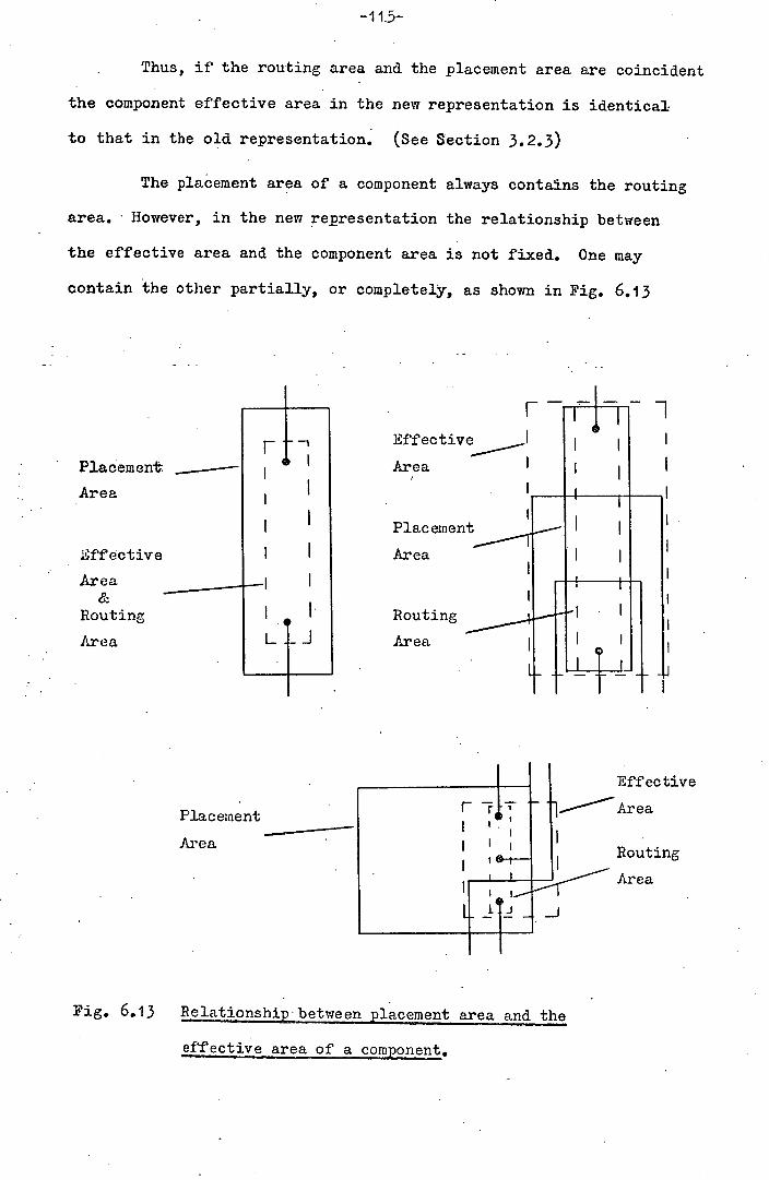
-1 1.5-
Thus, if the routing area and the placement area are coincident
the component effective area in the new representation is identical
to that in the old. representation. (See Section 3.2.3)
The placement area of a component always. contains the routing
area. However, in the new representation the relationship between
the effective area and the component area is not fixed. One may
contain the other partially, or completely, as shown in Fig. 6,13
Placement
Area
Effective
Area &
Routing
Area
rI! 1
EffectivJ i I Area I
I -
Placement I Area
:::ing _Ii
Area
LL
Placement
Area
Effective
Area
Routing
Area
Fig. 6.13 RelationshiE between placement area and the
effective area of a component.
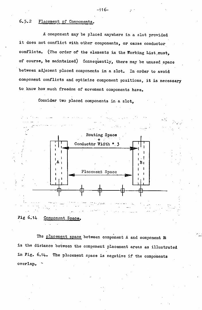
-i1 6- 1- .
6.5.2 Placement of Components.
A component may be placed anywhere in a slot provided
it does not conflict with other components, or cause conductor
conflicts. (The order of the elements in the Working List,must,
of course, be maintained) Consequently, there may be unused space
between adjacent placed components in a slot. In order to avoid
component conflicts and optimise component positions, it is necessary
to know how much freedom of movement components have.
Consider two placed components in a slot,
Placement Space
Fig 6 0 11. Component Space.
The placement space between component A and component fl
is the distance between the component placement areas as illustrated
in Fig. 6.14. The placement space is negative if the components
overlap.. -
-11.7--
Between A and B in the Working List there may be,
conductors, circuit nodes, and unpiaced components. Space must be
left between A and B for these elements to be routed up to higher
slots. The routing space between A and B is the distance between
the component effective areas less the space required by conductors
between A and B in the Working List.
The routing space between two components can be greater than
the placement space. This is illustrated. in Fig. 6.15 in which the
placement space is zero, but there is still space for conductors
between A and B. - -.
Routing .. .
Space.
---
11!I!I
Fig. 6.15 Example of placement space greater than routing space.
The smaller of the placement space and the.routing space
between tw components determines the maximum distance that either
of the components may moved toward each other, without causing
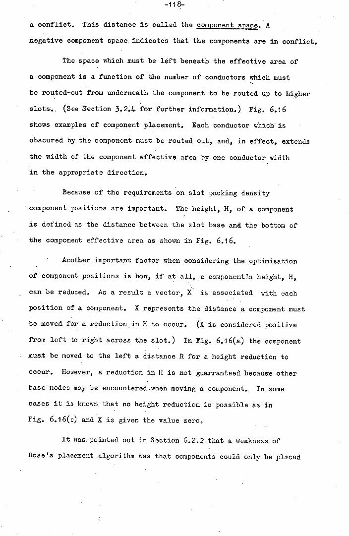
-118-
a conflict. This distance is called, the component space. A
negative component space indicates, that the components are in conflict.
The space which must be left beneath the effective area of
a component is a function of the number of conductors which must
be routed-out from underneath the component to be routed up to higher
s1ots.. (See Section 3.2.4 for further information.) Fig. 6.16
shows examples of component placement. Each conductor which is
obscured by the component must be routed out, arid., in effect, extends
the width of the component effective area by one conductor width
in the appropriate direction.
Because of the requirements on slot packing density
component positions are important. The height, H, of a component
is defined as the distance between the slot base and the bottom of
the component effective area as shown in Fig. 6.16.
Another important factor when considering the optimisation
of component positions is how, if at all, a components height, H,
can be reduced. As a result a vector, X is associated with each
position of a component. X represents the distance a component must
be moved for a.reduction in H to occur. (x is considered positive
from left to right across the slot.) In Fig. 6.16(a) the component
must be moved to the left a distance R for a height reduction to
occur. However, a reduction in H is not guarranteed becaus:e other
base nodes may be encountered .when moving a component. In some
cases it is known that no height reduction is possible as in
Fig. 6.16(c) and X is given the value zero.
It was. pointed out in Section 6.2.2 that a weakness of
Rose's placement algorithm was that components could only be placed
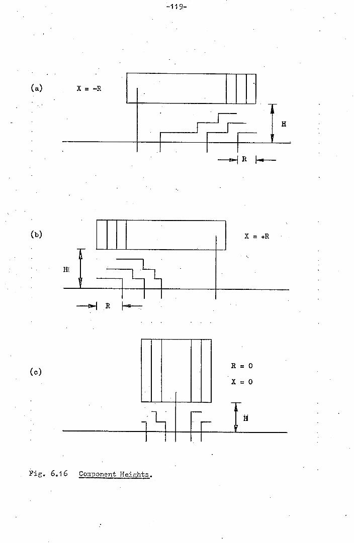
-19-
(C)
Fig. 6.16 Component Heijhtz.
-12O-
on a single base node, causing conductor routing as shown in
Fig. 6 *- 2(b). This has been modified such that if a branch component
(2-pin component) is connected to-two adjacent base nodes, one of
the base nodes is treated as an ACC. This approach allows both
conductors to be routed to the components within the slot.
6.5.3 Resolving Component Conflicts.
As described in Section 6.4.2 a Trial Placement is
performed on a combination of components from the Selection List.
At the start of the Trial Placement of a particular combination.
most of the components in the combination are, in general, already
placed in the slot as a result of the previous Trial Placement.
All that is needed is to remove one or two of the components from
the slot (if necessary) and place one or two new components. The
order of the components in the slot is fixed by the order in the
Working List. Consequently, it is known between which of the
components placed in the slot the new component(s) must be placed.
If there is insufficient component space for a new component to be
inserted the adjacent components must be moved to avoid conflicts.
However, the movement of adjacent components may, in turn, cause :
further conflicts. It may be deduced that a new component can
cause every component in the slot to be moved for it to be inserted.
This is very inefficient, especially if, after moving all the
components, there is insufficient space for the combination within
the slot. This situation is avoided by initially ignoring conflicts
caused by inserting new components, and calculating the slot space
with the new components in the slot.

-121-
The slot space is given by,
Slot Space =
(Component Space).
where, N is.the number of components; placed in the slot. If the
slot space is negative the combination is too big for the slot, and
no further processing is necessary, and the next combination is
considered. If the slot space is positive or. zero the combination
will fit into the slot, and therefore any conflicts which exist
must be resolved.
It is desirable that the resolving of conflicts be as
efficient as possible. In addition, the components which were also
in the previous component combination will, in general, have been
optimised with respect to position, and, consequently, should not
be moved unnecessarily i.e. it is desirable to avoid unnecessary
disruption of the las:t Trial Placement. The remainder of this
section is a description of the method used to resolve conflicts.
All the components placed in the slot are stored in a list
called the Trial Placement List. The order of components in the
list corresponds to the order of the components from left to right
across the slot. The slot space is constant irrespective of
component positions because it is the sum of positive and negative
component spaces. The task of resolving component conflicts may
be considered to be the elimination of all negative component spaces.
This implies that the sum of positive component spaces must not
exceed the slot space.
Each component in the Trial Placement List is considered
-122-
in turn, and any conflicts .are resolved. By restricting the sum of
component spaces of components which have been considered to less
than the slot space, all conflicts can be resolved in a single
pass through the Trial Placement List. If the sum were allowed
to exceed the - slot space, conflicts, which could not be resolved,
would inevitably occur when positioning components further 'down'
the Trial Placememt List. (i.e. further across the slot.)
The position of each component is examined in relation to
the positions of the adjacent components in the slot.
Fig. 6.17 Comj2onent not in conflict.
Assuming a component, C, is currently under consideration,
Fig. 6.17 shows a situation in which C is not conflicting with the
next component in the Trial Placement List, N, or the previous
component in the Trial Placement List, P. The component spaces
between component C and components P and N are termed Spc and Son,
respectively.
There are a number of possible relationships between P,
C, and N depending on the magnitudes and signs of Spc and Son and
also on whether the addition of Spc to the sum of component spaces
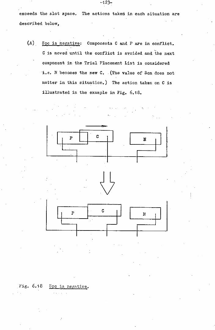
-123-
exceeds the slot space. The actions takezi in each situation are
described below,
(A) Spc is negative: Components C and P are in conflict.
C is moved until the conflict is avoided and the next
component in the Trial Placement List is considered
- i.e. -N becomes the new C. (The value of Son does not
matter in this situation.) The action taken on C is
illustrated in the example in Fig. 6.18.
Fig. 6.18 Speis negat ive .
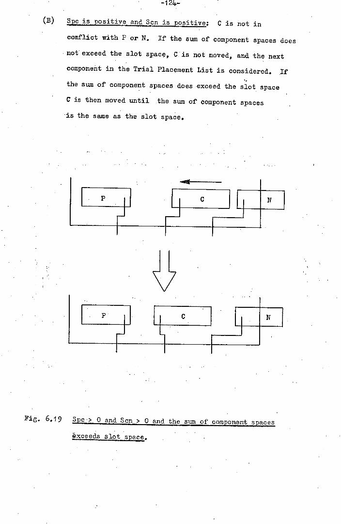
-124-
(B) Spc is positive and Sen is positive: C is not in
conflict with F or N. If the sum of component spaces does
• not exceed the slot space, Cris not moved, and the next
component in the Trial Placement List is considered.. If
the sum of component spaces does -exceed the slot space
C is then moved until the sum of component spaces
is the same as the slot space.
Fig. 6.19 pc> 0 and Sen > 0 and the sum of component spaces
xceeds slot space.
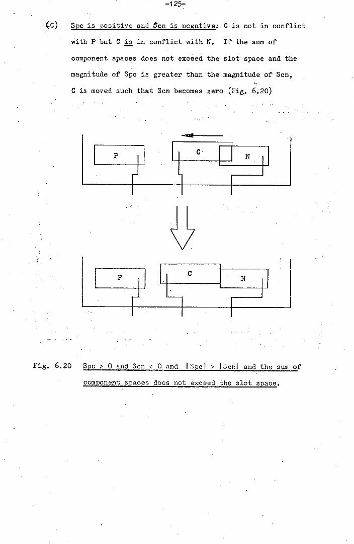
-1 25-
(C) Spcis C is not in conflict
with P but .0 is in conflict with N. If the sum of
component spaces does not exceed the slot space and the
magnitude of Spe is greater than the magnitude of Scn,
C is moved such that Scn becomes zero (Fig. 6.20)
Fig. 6.20 Spc >0 and Scn < 0 and ISpcJ > IScnI and the sum of
component spaces does not exceed the slot space.
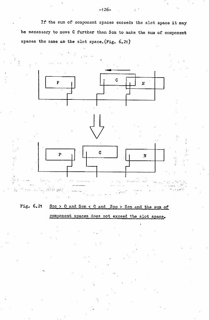
-126-
If the sum of component spaces exceeds the slot space it may
be necessary to move C further than Sen to make the sum of component
spaces the same as the slot space. (Fig. 6.21)
J p
Fig. 621 Spc > 0 and Son < 0 and Spc > Son and the sum of
component spaces does not exceed the slot space.
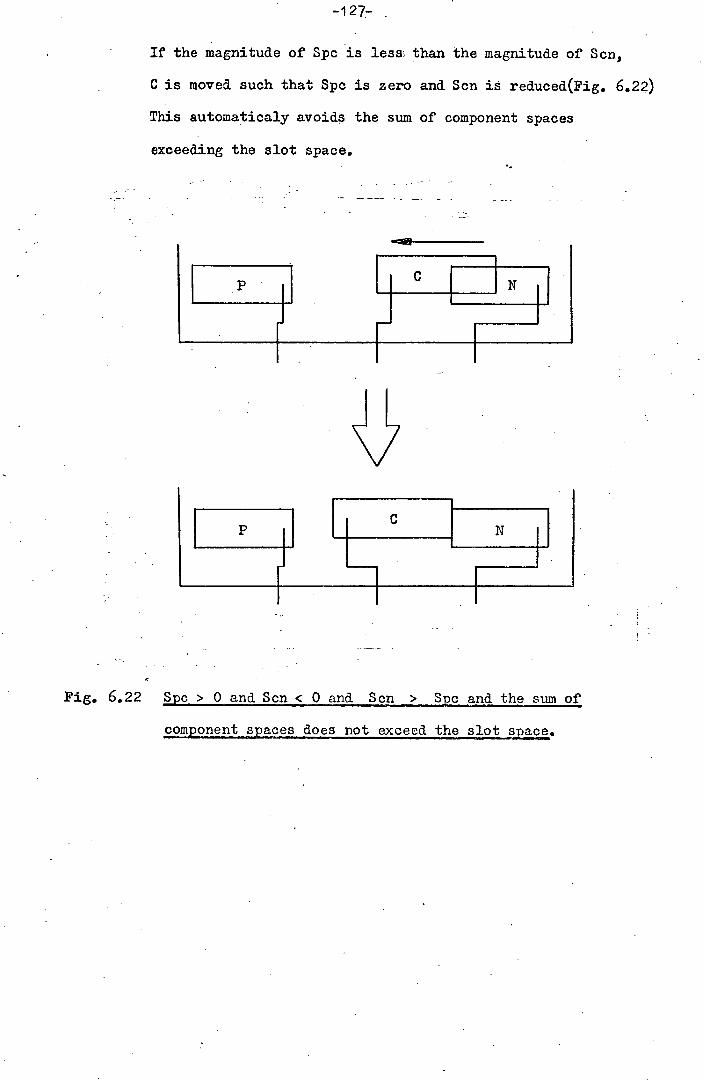
-127-
If the magnitude of Spc is less than the magnitude of Son,
C is moved such that Spo is zero and Son is reduced(Fig. 6.22)
This automaticaly avoids the sum of component spaces
exceeding the slot space.
Fig. 6.22 Spc > 0 and Scn < 0 and Sen > Spçnd the sum of
component spces does not exceed the slot space.

The method of resloving components-described above has the
following characteristics,
(i) if, as often occurs, no components are in conflict, then
no components are moved, and very little computation is
required,
the disruption of the current slot layout is kept to a
minimum .,
all conflicts may be resolved by a single pass through the
Trial Placement List,
the method is efficient and suited to computer implementation.
6.5.1+ 01ILimisinjComponent Positions.
At this stage all the components for Trial Placement are
placed in the slot, and there are no conflicts The object is to
improve the component positions, without öausing conflicts, prior
to the calculation of the slot packing density, Ds.
The height, H. of a component , as defined in Section 6.5.2
is a useful measure of the 'goodness;' of the position of a component.
Fig, 6.23 shows the two possible positi.:ons of a component,. c in
a slot. (The rectangles are the component effective areas)
In Pig. 6.23(a) component C is positioned such that two
conductors have to be routed out from under it. This results in a
large component height llc. The conductor connecting C to the slot
base is unnecessarily long, as are the-conductors which are routed
from under C. In addition these conductors are positioned much
more closely together tha.. in the slot base, which restricts
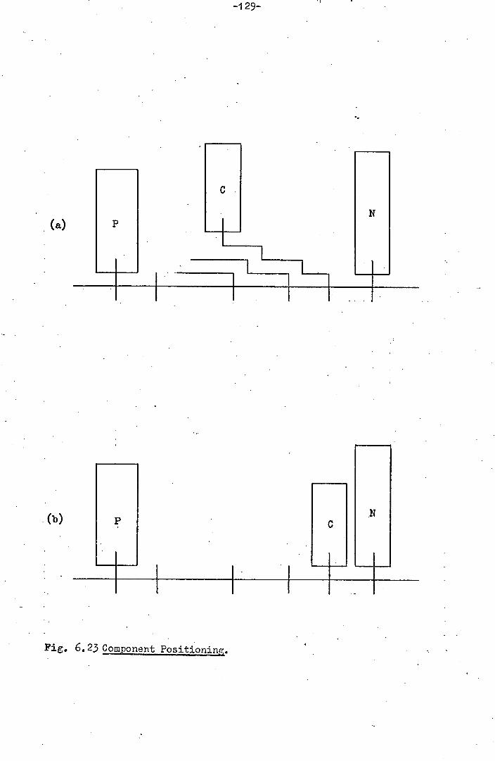
-1 29-
(b)
Fig. 6.23 Com2onent Positioning.
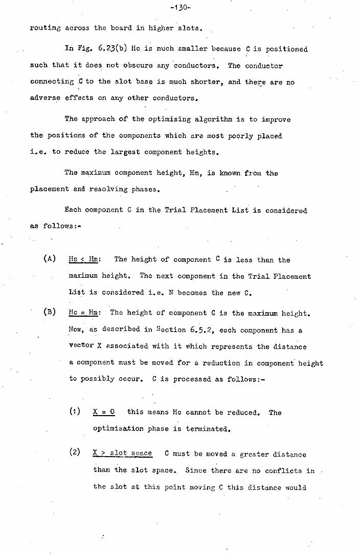
-130-
routing across the board in higher slots.
In Fig. 6.23(b) He is much smaller because C is positioned
such that it does not obscure any conductors. The conductor
connecting .0 to the slot base is much shorter, and there are no
adverse effects on any other conductors.
The approach of the optimizing algorithm is to improve
the positions of the components which are most poorly placed
i.e. to reduce the largest component heights.
The maximum component height, Jim, is known from the
placement and resolving phases. -
Each component C in the Trial Placement List is considered
as follows: -
He < Jim: The height of component C is less than the
maximum height. The next component in the Trial Placement
List is considered i.e. N becomes the new C.
He = Jim: The height of component C is the maximum height.
Now, as described in Section 6.5.2, each component has a
vector X associated with it which represents the distance
a component must be moved for a reduction in component height
to possibly occur. C is processed as follows:-.
(i) X = 0 this means He cannot be reduced. The
optimisa.tion phase is terminated.
(2) X> slot' space C must be moved a greater distance
than the slot space. Since there are no conflicts in
the slot at this point moving C this distance would

-131-.
inevitably cause conflicts which could not be
resolved. The optimisation phase is terminated.
(3) X < slot space , Xi:'O: there is a possibility that
He could be reduced without incurring conflicts- which
could not be resolved. C is moved a distance X.
If the new component height of C.is He', then, if,
He' Hm: the height of C has not been reduced.
C is moved back to its old position and the
optimisation phase is terminated.
Hc':< Jim: The height of C has been reduced.
There are two possibilities at this point;
(i) C is in conflict with an adjacent component:
In this case the adjacent component is moved
until there is no conflict. If this component
in turn causes further conflicts these are also
resolved. If at any stage Jim is exceeded then
no further action is taken - the components are
moved back to the old positions and the
Optimisation phase ceases. Otherwise, when no
conflict occurs,
(2) C is not in conflict with an adjacent component:
the next component in the Trial Placement List
is considered. i.e. N becomes the new C.
If all the components in the Trial Placement List have been
considered, and the component heights have been reduced where necessary
then Jim is reduced by one conductor 'iiath, and the whole procedure

-132--
is repeated until no improvement is possible.
The following points about the above algorithm are worth
noting,
it is specifically aimed at improving the placement of the
most poorly placed components,
it improves the conductor routing,
it increases the slot packing density, Ds,
it is efficient and suited to computer implementation.
6.6 Completion of the Component Selection and Placement Phase.
At this stage Trial Placements have been performed on all
Selection Lists and the component combination with the highest packing
density, Ds, is placed in the slot. In order to complete the
Component Selection and Placement phase it is necessary to develop
the selected components and place the conductor ends.
6.6.1 Developing Selected Components.
This involves examining the mesh to determine which
conductor branches, circuit nodes etc., are connected to a component.
A selected component is replaced in the Working List by the elements
of the mesh which it generates so that they may be considered in
higher slots.
This process. is performed in the same manner as in Rose's
implementation.
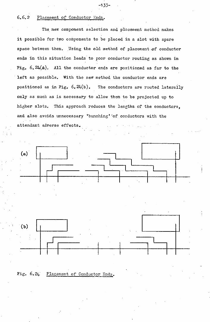
-133-
6.6.2 Placement of Conductor Ends.
The new component selection and placement method makes
it possible for two components to be placed in a slot with spare
space between them. Using the old method of placement .of conductor
ends in this situation leads to poor conductor routing as shown in
Fig. 6.24.(). All the conductor ends are positioned as far to the
left as possible. With the new method the conductor ends are
positioned as in Fig. 6.24(b). The conductors are routed laterally
only as much as is necessary to allow them to be projected up to
higher slots. This approach reduces the lengths of the conductors,
and also avoids unnecessary 'bunching' of conductors with the
attendant adverse effects. - - -
(a)
(b)
Fig. 6.24 Placement of Conductor Ends.
Chapter 7. Other Modifications to Rose's System.
The most significant changes to Rose's system, after the
new component selection and placement algorithm, are the modified
method of inserting rejected branches in PLANAR, and the new system
of manual interaction in LAYOUT.
7.1 The Insertion of Rejected Branches in PLANAR.
As described in Chapter 3 a mesh of a circuit graph is
constructed in two independent stages. During the first stage a
planar mesh is constructed and component branches and link branches
are rejected. During the second stage rejected branches are inserted
using inter-pin spaces, introducing branch crossings into the mesh.
7.1.1 Discussion of Rose's Method of Branch Insertion.
The rejected branches are all stored in a list. The aim
of the branch insertion algorithm is to insert all of the rejected
branches. However, this is not alwys possible because branch
insertion is constrained by the form of the mesh, and the
distribution and magnitudes of inter-pin spaces. The insertion of
each branch affects both of these characteristics of the mesh i.e.
the branches are interdependent with respeôt to insertion. As a
result the problem of branch insertion is non-trivial.
The insertion of a branch can only reduce the probability
of being able to insert subsequent branches. Consequently, Rose
organises the list such that the component branches are separated
from the link branches and inserted first. This is done because
link branches, which cannot be inserted into the mesh, can be
-135-
inserted into the final layout as wire-jumpers, whereas this is not
possible with component branches.
Each branch in the list is considered independently, in turn,
and inserted such that it introduces the minimum number, of component/
conductor crossings. The only consideration given to the interdependence
of branches is the separation of component branches and link branches
to reduce the probability of rejecting components from the final
layout.
This method results in unnecessarily large numbers of
component/conductor crossings and the unnecessary rejection of
branches. The effect of large numbers of crossings is probably more
severe than that of rejecting branches, because the performance of
the LAYOUT program is very much a function of the ratio of the number
of components to the number of crossings in a circuit.
7.1.2 Modified Method of Branch Insertion.
The branch insertion method was modified to reduce the
number of branches omitted unnecessarily from the mesh and the number
of component/conductor crossings necessary to insert a given number
of branches.
The insertion of a branch affects the insertion of subsequent
branches by,
altering the form of the mesh i.e. changing the number of
branches, the structure of the regions etc.
reducing the inter-pin spaces of components it crosses.
The optimum optimum branch insertion is considered to be the
insertion of the maximum number of branches with the minimum number
of crossings. To achieve this optimum, the effects of both (i) and
(2) must be considered.
Consideration- of the effects of (i) would require a detailed
analysis of the structure of the mesh, and for this reason was
considered inappropriate. It is possible, however, to consider the
effect of (2) without resorting to such detailed analysis.
The cost of inserting a branch is considered to be the
number of component/conductor crossings required for its insertion.
The modification to Rose's method is based upon the assumption that
the overall cost of inserting a number of branches into a mesh is,
in general, reduced if the branches are inserted in order of increasing
cost. This assumption is justified by the results shown in Chapter 8.
The list of rejected branches is separated into two lists -
one for component branches and one for link branches. Each list
is processed in the same way, and the component list is processed
first. The procedure is as; follows
(i) Associate with each branch a cost representing the number
of crossings necessary to insert it into the mesh.
Insert the set of branches with the lowest cost.
End the procedure if the list is empty, otherwise repeat
the procedure.
The interdependence of branches in the minimum cost set is
ignored.

-137-
The program user is given a limited amount of control
over the insertion of link branches. This is achieved by the user
typing in a number which represents the relative desirability of
jumper wires and component/conductor crossings. The number is
termed the crossing/jumper ratio. The link branches are inserted
in order of increasing cost until, the cost is equal to the
crossing/juniper ratio, after which no further link branches are inserted.
This facility provides a crude form of interaction with the PLANAR
program.
7.2 Manual Interaction in LAYOUT.
Rose's system of interaction is described in Section 3.2.6,
and discussed. in Sections 5.2 and 5.4.
Any system of manual interaction which d.oes. not involve major
changes to the layout method must satisfy the following constraints,
(i) the layout must correspond directly to the mesh. Thus,
no rerouting of conductors which could alter this
relati9nship is permitted..
A layout is constructed from a number of slot layouts.
This implies that interaction must be related to individual
slots rather than to the complete layout.
Only components directly connected to conductors in the
Base List of a slot may be placed in that slot. Thus, the
set of components which may be placed in a slot becomes
very restricted.
-138-
The combined effect of (1), (2), and (3) is to very severely
restrict the scope for interaction. However, it was considered that
a more powerful system of interaction could be introduced which still
satisfied the above constraints.
There are three interaction states in the new system called
the Layout State, the Slot State, and the Display State.
The interaction modes available in each state are displayed
on the 340 Display screen in a vertical column to the right of the
printed circuit board outline.
7.2.1 The Layout State.
The purpose of the Layout State is to enable the user to
control the automatic layout process, I/o, and the selection of
slots for modification.
In order to use a particular interaction mode, the user
points the light pen at the required mode, and the program
acknowledges this selection by doubling the size of the mode word.
He then points the light pen at EXECUTE to confirm his selection.
No action is taken until the mode selection is confirmed.
• The following modes are available:—
DATA
This mode enables the user to specify different data
files without terminating the program.
PLOT..
By using this mode hard copy output of any layout, or
part layout, displayed on the screen may be obtained, usually on

-139-
a Calcomp drum plotter, but a Tektronix 4010 display and Hard
Copy- Unit can be used.
DUMP.
If a particular layout form incorporates a-number of
modifications in certain slots, and the user wishes to make some
changes to a lower slot, he will lose the results of the previous
modifications. This mode enables the user to store the current
layout state at any time on disc, and reinstate it later, if he so
wishes.
COMPLETE.
This mode instructs the program to continue automatically
and complete the layout. As each slot is processed it is displayed.
If the user does not require the program to complete the whole board
this process of automatic layout can be halted by pointing to any
of the mode words. The program then waits for further instructions.
EXIT.
Not unreasonably, this mode allows, the user to terminate
his program run, and obtain information on execution times etc.
CHAIGE.
In order to make a modification to the layout it is
necessary to identify the slot within which the necessary alteration
is to be made. This is done by selecting CHANGE and then pointing
the light pen at any component within the required slot. After
confirmation of the choice all components and conductors in slots
above the selected slot are deleted, and the mode words corresponding
to the Slot State of interaction are displayed. Thus, CHANTGE mode
is the means by which the user is able to transfer from the Layout
-111.0--
State of interaction to-the Slot State of interaction.
DISPLAY.
The mode words of the Layout State are replaced by the
mode words of the Display State, and control is transferred to the
Display State.
7.2.2 The Slot State.
The purpose of the Slot State is to enable the user to
make modifications to the layout form within a particular slot.
The choice of components to be placed in a slot is limited
to those components directly connected to conductors in the base
list of the slot. To give the user a clear picture of the
possibilities available to him, components which could be placed
in the slot, but are not currently placed, are displayed. These
components are positioned such that there is a vertical line between
the component pin and the appropriate base conductor. If a component
is displayed above the slot, it is termed 3pLaced. If a component
is currently placed in the slot it is termed placed.
The interaction modes at this level are used to form
instructions which are 'interpreted' by the program, and modify its
action with respect to component selection, and placement. The
instructions are set up by first selecting a mode, and then pointing
the light pen at the component(s) to which the mode is to be applied.
A modification is made when all the instructions relating to that
modification have been set up.
The program acknowledges an instruction by changing the

114-1
display of the particular component. Thus, the user is able to
'read' the instructions off the display, and does not have to remember
them.
The following modes are available;-
EXECUTE.
When the set of instructions representing a particular
modification to the slot layout have been generated, the user selects
this mode to implement them.
FIX and FREE.
A placed component's position in a slot may be fixed or
freed. If the component is free, it may be moved by the program
during execution, to reduce the packing density of the slot, or
perhaps to allow room for an unpiaced component to be inserted.
If it is fixed the component may not be moved. The display intensity
of free, 'placed components is made lower than that of fixed,
placed, components.
If a component is unplaced, FIX and FREE apply to its
orientation. When the program considers an unpiaced component for
placement, it tries all the possible orientations, and selects the
one it considers most appropriate. However, a particular
orientation may be required for a component in which case it is
necessary to fix the orientation prior to the execution of the slot.
The fact that a component's orientation is fixed, is indicated to
the user by underlining the component's name.

-1
OMIT andand SELECT.
The user can prevent the program from considering a
particular unpiaced component for placement by omitting it.
Similarly, SELECT permits selection and placement of acurrently
unpiaced component . The display intensity of selected components
is greater than that of omitted components;.
DELETE.
This mode applies only to.placed components. When a
component is deleted it is removed from the slot, and displayed above
it. Thus the component is changed from placed to unpiaced. It is
automatically OMITted to prevent its reinsertion during the
execution of the slot.
MOVE.
This mode enables. the user to choose the position of a
placed component in a slot. The component is "dragged' across the
screen using a light pen. (The conductors connected to the component
do not move with the component.) During execution the program attempts
to place the component at the selected position. The program does
not allow the user to move a component out of a slot, or to overlap
components and conductors. If the user selects a position in which,
conflicts would arise with existing place components and conductors;,
or where an alteration to the graph data structure is involved, the
program does not place the component at this position, but places
it as near as. possible, without causing conflicts. The program
automatically moves free components out of the way of a component
which has been repositioned, but no components are automatically
deleted.

11f3
ORIENT. -
Before fixing the orientation of an unpiaced component
it may be necessary to rotate the component. When a component is
selected in.ORIENT.mode, it is rotated in an anticlockwise direction
to the next permissable orientation. When the required orientation
is reached the component orientation can be fixed.
ALL
Selecting ALL has the same effect as selecting all of
the components. independently.
COMPLETE.
This mode instructs. the program to continue the layout
automatically, and returns control to the Layout State of interaction.
DISPLAY.
The mode words of the Slot State are replaced by the
mode words of the Display State and control is transfered to the
Display State.
7.2.3 The Display State.
The purpose of the Display State is to enable the user to
control the layout information displayed on the screen.
The new component descriptions make it possible for
conductors to be routed under component bodies. (Component placement
areas) As a result, lines representing conductors may be coincident
with lines representing component outlines in the display of the

layout. This makes the layout form difficult to comprehend. To
alleviate this problem the user is given independent control over
the displaying of certain elements of the layout. To identify an
element the user selects one of the following mode words:-
COMPS.
This mode identifies the component outlines which
correspond to the component placement areas.
COND1JC.
This mode identifies the --lines representing the
conductors, including the component pads.
NAMES.
This. mode identifies the component names.
Having selected an element the user can attribute, to it one
of three display states by selecting one of the following mode words;:-
BRIGHT.
In this state an element is displayed brightly on the
screen. (Intensity 6 in the range I to 7 for the 31+0 Display).
DIM.
In this state an element is displayed dimly on the screen.
(Intensity 3)

REMOVE.
In In this state an-element is not displayed.
There are two other mode words in the Display State,
FLICKER.
When large circuits are displayed i.e. when there is
a great deal of information on the screen, the flicker of the 34.0
Display becomes very significant, making comprehension difficult.
To alleviate this problem the user may.. remove all of the layout
below a certain slot thus reducing the amount of information on
the screen and the flicker. The user accomplishes this by first
selecting the FLICKERmode word, and then identifying a componetit
in the required slot. (All slots below this slot are erased from
the screen)
RETUPJ.
This mode returns control to the state from which the
Display State was entered i.e. either the Slot State or the Layout
State.
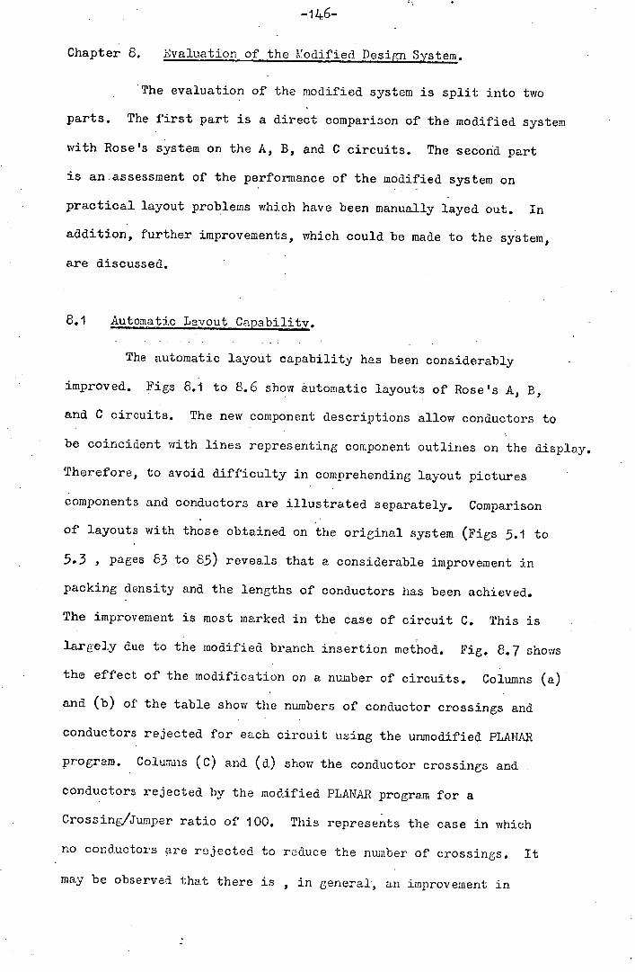
Chapter 8. Evaluation of the Modified Design System.
The evaluation of the modified system is split into two
parts. The first part is a direct comparison of the modified system
with Rose's system on the A, B, and C circuits. The second part
is an assessment of the performance of the modified system on
practical layout problems which have been manually layed out. In
addition, further improvements, which could be made to the system,
are discussed.
8.1 Automatic Layout Capability.
The automatic layout capability has been considerably
improved. Figs 8.1 to 8.6 show automatic layouts of Rose's A, B,
and C circuits. The new component descriptions allow conductors to
be coincident with lines representing component outlines on the display.
Therefore, to avoid difficulty in comprehending layout pictures
components and conductors are illustrated separately. Comparison
of layouts with those obtained on the original system (Figs 5.1 to
5.3 , pages 83 to 85) reveals that a considerable improvement in
packing density and the lengths of conductors has been achieved.
The improvement is most marked in the case of circuit C. This is
largely due to the modified branch insertion method. Fig. 8.7 shows
the effect of the modification on a number of circuits. Columns (a)
and (b) of the table show the numbers of conductor crossings and
conductors rejected for each circuit using the unmodified PLANAR
program. Columns (C) and (d) show the conductor crossings and
conductors rejected by the modified PLANTAR program for a
Crossing/Jumper ratio of 100. This represents the case in which
no conductors are rejected to reduce the number of crossings. It
may be observed that there is , in general, an improvement in
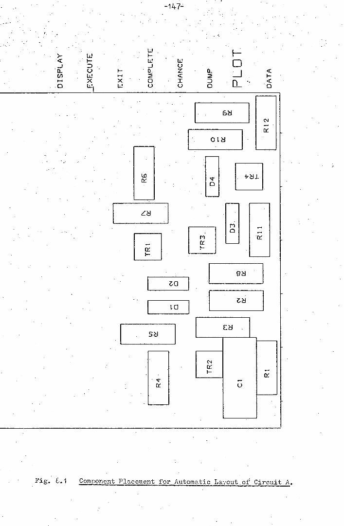
-1 L7-
0
60
f LoJ
Fig. 6. 1 Component Placement for Automatic Laiout of Circuit A.
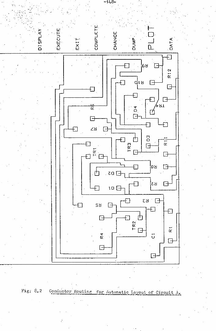
Fig. 8. 2 Conductor Routing for Automatic La-out of Circuit A.
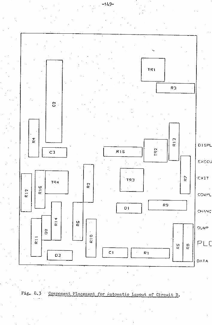
_LC3
N
-14.9-
N C.)
L .R 15 '1 LY
TR3
Lo1 LR9 1
0
Ln co It of
iH11LR1_H
Dl SPL
ECU
E)< I I
CO M C?L
CHANC
0 U MD
PLC
DATA
Fig.. 8.3 ont1iacinent for Automatic Layout of Circuit B.
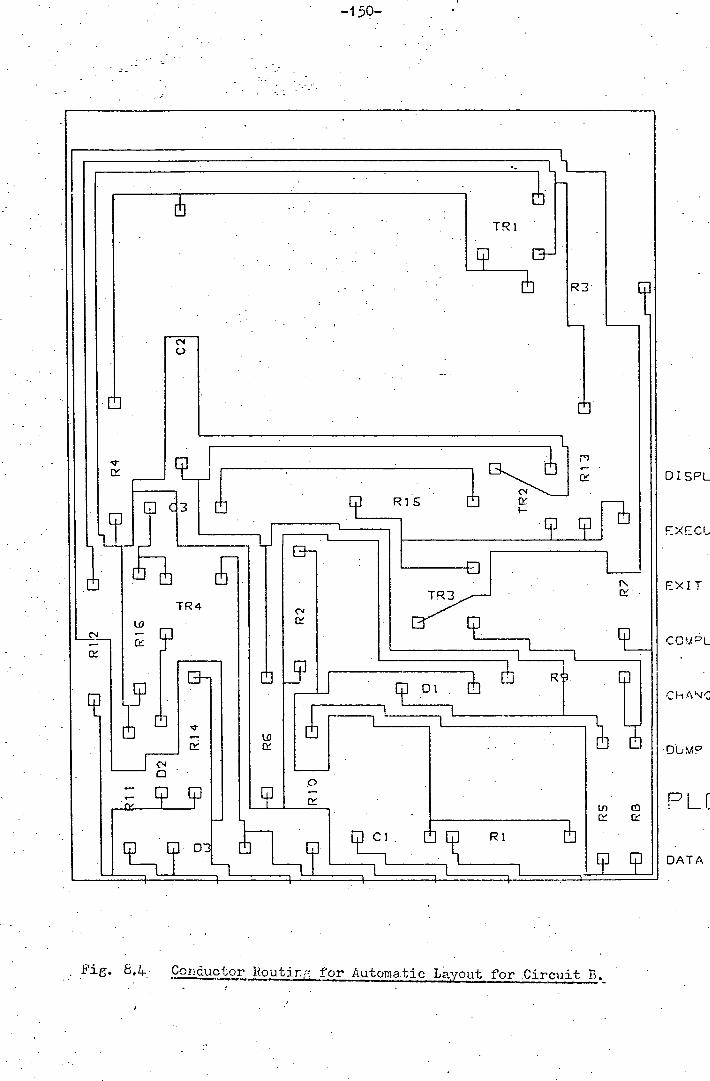
jI
fl is ['1Ly-
Q .
I TR4
L
U)
co
Co nductor 2irfor Automatic Layout. for Circuit B.
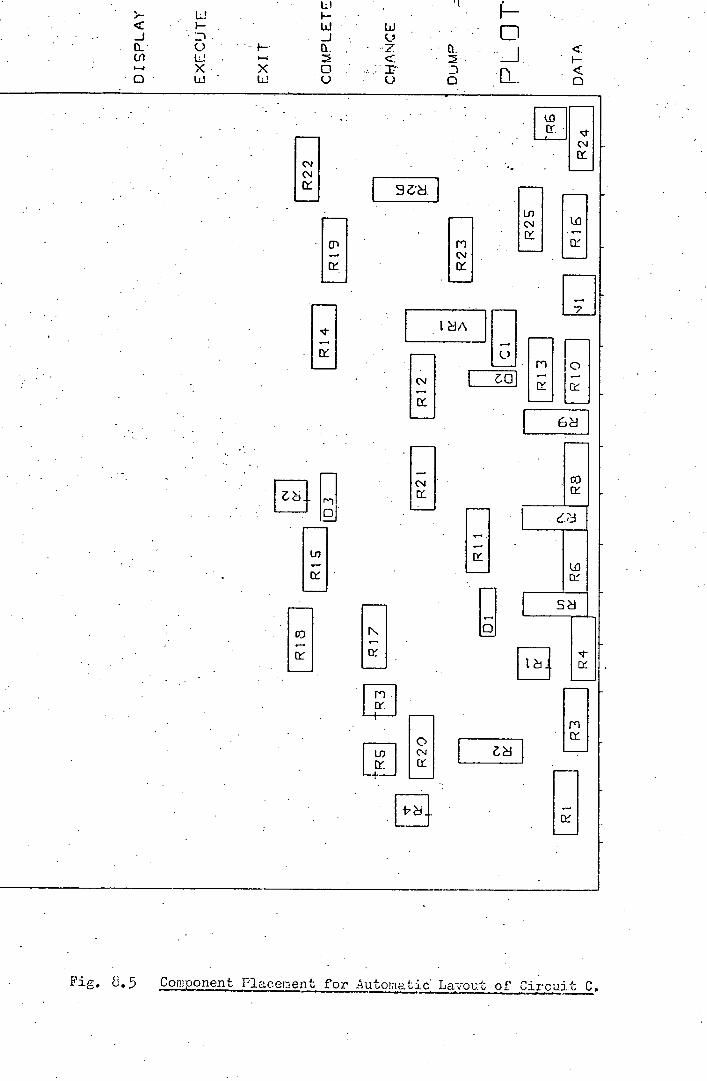
• >- .L2 1—
LL 0 4— Cl • Z •' (L . .. p 01 U. • —J. 1- I.-.' '(. I-I • •• r• - -
H • ul
(sz
: H' Df
LèJA
710
Hr11 co
La ri
sj
[ad.
_ n [j
Fig. 8. 5Com2onentP1acementforAutornaticLavout of Circuit C.
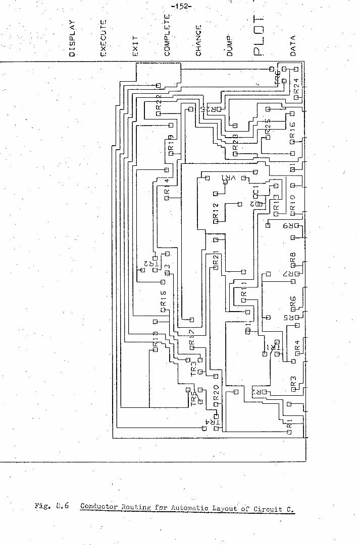
U! • •• <••
••• _J • ••
• 0 ($1
• ••• • x
0 Li
-152- • •l
LI '1– ••
• w w _J U
F- tL • Z ti. '-4 • • • —I X 0 . I U 0 0 0 0
J,-~j
1 , f~~
LY
El
U,- -
Lf3J/\ Lr4j
ri
cli
LY
13
cr
F -El LLII
t7 èI I
Fig. 6.6 Conductor Routing fur Automat G ic Layout of Circuit C.
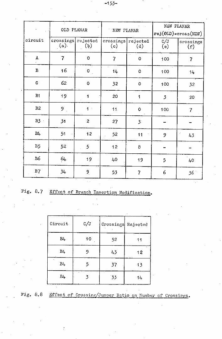
-153—
-
circuit
OLD PLANAR NEi PLANAR NW PLANAR
rej (OLD) =cros s (NEvT)
crossings rejected crossings (c)
rejected (d)
c/J (e)
crossings (f)
A 7 0 7 0 100 7
B 16 0 14. 0 100 14.
C 62 0 32 0 100 32
BI 19 1 20 1 3 20
B2 9 1 11. 0 100 7
B3 31 2 27 31 - -
134. 51 12 52 11 9 43
B5 52 5 12 8 - -
B6 64.. 19 4.0 19 5 4.0
B7 34. 9 53 7 6 36
Fig. 8.7 Effect of Branch Insertion Modification.
Circuit c/j Crossings Rejected
134 10 52 11
B4 9 43 12
134 5 37 . 13
P4 3 •33 14.
Fig. 8.8 Effect of CrossinjJuinper Ratio on Number of Crossings.
-151f-
performance. In columns (e) and (r) the Crossing/Jumper ratio has
been used to equate the number of Conductors rejected by the modified
system to the number rejected by. the original system. (This is not
possible for circuits B3 and B5 since the new system rejects more
conductors than the old system). Thus, only the number of crossings
need be compared. It maybe observed that there is, in general,
a reduction in the number of crossings required. As shown in Fig. 8.8
the Crossing/Jumper ratio can be used quite effectively to reduce
the number of conductor crossings required for a circuit.
The system has not - been extended to cater for non-rectangular
boards, multiple edge-connectors or multiple conductor widths.
(These extensions are discussed in Section 8.6)
8.2 Interaction Capability.
The new system of interaction improves the interaction
capability of the design system. A component's position within a
slot may be selected, provided it does not cause conflicts to occur,
In addition, layouts, or part layouts, may be stored on disc, and
reinstated at the user's convenience. However, the scope of
interaction is very restricted due to the constraint that the mesh
imposes on the layout. (This is further discussed in Chapter 10)
8.3 Com2utational Efficiency.
The execution times to produce the layouts of the A. B,
and C circuits shown in Figs 8.1 to 8.6 are given in Fig. 8.9
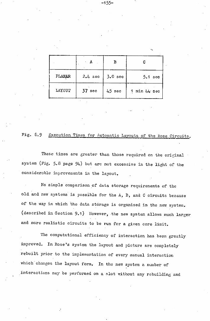
-155-
-A, B C
I PLANAR 2,4 sec 3.0 sec 5.1 sec
LAYOUT 37 see 45 sec I min 144 sec
Fig. 8.9 Execution Times for Automatic Layouts of the Rose Circuits.
These times are greater than those required on the original
system (Fig. 5.8 page 94) but are not excessive in the light of the
considerable improvements in the layout.
No simple comparison of data storage requirements of the
old and new systems is possible for the A, B, and C circuits because
of the way in which he data storage is organised in the new system.
(described in Section 9.1) However, the new system allows much larger
and more realistic circuits to be run for a given core limit.
The computational efficiency of interaction has been greatly
improved. In Rose's system the layout and picture are completely
rebuilt prior to the implementation of every manual interaction
which'changes the layout form. In the new system a number of
interactions may be performed on a slot without any rebuilding and

-156-
the rebuilding process has been simplified by eliminating the
need to select and place components during rebuilding. In addition,
new pictures are only generated for new slot placements (described
in Chapter 9)
8.4. Interaction Efficiency.
The new interaction system allows the user to communicate
more effectively with the layout. The limitations of the form of
the mesh and the slot are made clear by the displaying of unpiaced
components above the components placed in the slot.
All the layout modifications are made using instructions
set-up with a light-pen. Complex modifications may be set-up with
a series of instructions and all of the instructions which modify
the layout form are reversable. In addition, the modifications to
be performed can be easily 'read off' the screen because of the
visual feedback provided in the form of varying intensities etc.
The system response is quite good because no rebuilding
of the layout between interactions on the same slot is required.
However, the PDP-10 system is timeshared and as a result the
response time is a function of the system loading at the time of
program execution.
8.5 Performance on Practical Layout Problems.
A number of practical layout problems have been tried on
the system. The layouts obtained for four such circuits are given
in Appendix 1. For the purpose of comparison the circuit diagrams
and manual layouts are provided for each circuit. The layouts in
the Appendix show that reasonable layouts of practical circuits may
-157-
be obtained using the system. The packing densities are acceptable
for many applications and the execution times are not prohibitive.
However, there are a number of factors which, in the author's opinion
make the system unsuitable for industrial implentation.
The interaction capability is 4adequate. This results from
the restriction that the layout must correspond directly to the
mesh. The form of the layout is restricted by the mesh and in
general any distortion of the initial automatic layout tends to
reduce the packing density of the layout and increase the lengths
of conductors.
The layout of components with more than three pins is very
poor. The PLANAR program is very inefficient at processing these
types of components and rejects large numbers of link branches.
The tendency is for components with more than three pins to have
their number of pins effectively reduced. The LAYOUT program is
also inefficient at processing components of this typo. This results
from two main factors,
, components are only placed on a single base node,
no routing of conductors between components in the Working
List is performed.
In general components with more than three pins are placed
very poorly and the associated, conductors tend to be unnecessarily
long.
-158-
8.6 Possible Improvements to the Modified System.
The system has been a 'test-bed' for ideas and has evolved
over a long period of time. Consequently, the developement has
been to a large extent 'history driven' In this section further
improvements which could be made to the system are briefly described.
8.6.1 Slot Layout.
As stated in Section 8.5 the system does not perform well
on subgraph components with more than three pins. To raise the
performance of the system to an acceptable level modifications in
the following areas would have to be made,
(i) Cojponent Selection.
Component connection numbers are used to influence the
selection of components. However, this connectivity relates base
elements to individual components. The connections between adjacent
components in, the Working List are not considered. This becomes
significant when laying out subgraphs because of the potentially
large numbers of conductors which can be generated. In order to
calculate the connectivity between components in the Working List
the components would have tobe developed prior to placement. More
significantly, from the point of view of execution time, component
connectivities would have to be calculated for each component,
combination.
(2) Placement of Components.
The placement of components could be improved by allowing
components to be placed on one or more base nodes and/or conductors.
This could could only be achieved by significant modifications to the
routines for developing a Working List from a Base List, and also
to the routines for developing and placing components.
(3) Routing of Conductors.
Both the routing of conductors and placement of components
could be improved by allowing conductors to be routed between
components in the Working List. However, the conductor routing
algorithm would have to be completely rewritten.
8.6.2 Extension to General Layout Capability.
The ability to represent effectively one-pin, and zero-pin
components and fix components anywhere on a board would allow the
general layout capability to be extended. This becomes apparent
when the following points are considered,
(i) board areas where component placement and conductor routing
is not permitted (termed obstructions may be represented
by one or more, zero-pin, components which are fixed in
'position on the board,
boards which are not rectangular may be 'constructed' by
positioning zero-pin components representing obstructions
about the perimeter of the board,
testing points and flying leads may be represented by
one-pin components which are fixed in position,
('i-) o the positions of critical components may be predetermined.

-160-
The implementation of zero pin and one-pin components
and the fixing of component positions is not trivial. It would
probably require,
(i) changes in component representation,
the capability of placing components in a slot without
connections to an element in a Base List,
a limited slot lookahead capability, to avoid conflicts
with obstructions when building a layout.
8.6.3 The Mesh Constraint.
As stated previously the form of the mesh tends to severely
limit the form of the corresponding layouts. An approach which can
be very easily implemented is to-construct a number of meshes by
starting the PLANAR - algorithm from different edge- connector nodes.
The mesh which produces the best initial layout can then be selected.
Fig. 8.9 shows the automatic layouts of meshes constructed by
starting from different edge-connector nodes of the A circuit. It
can be seen that there is considerable variation in packing density
However, this approach does not alleviate the major problem of the
inflexibility of the layout form during manual interaction.

, Fc cec± c w0a.
-161-
I- - 0• * 1_i
8
-
1~ Mi. 1 ~
II11i'tL_a IIIIII j
Iz
I-
. I
ro CI
I-
I
I I
I- 0
EL
I-.
I
-162-
Chapter 9. Computer Implementation.
This chapter is a description of the most important aspects
of the implementation of the modified design system. A description
of the implementation of Rose's system is given in 113J.
9.1 Data Storage.
In PLANAR a one-dimensional array is used to store'the mesh
data structure. The different types of nodes and branches are stored
as contiguous blocks of array elements, linked by pointers into rings
and lists to represent the mesh. In addition to the mesh data
structure each component type used in a circuit must have a master
component block. This block contains a description of the component
geometry i.e. component placement area, component routing area, pin
positions etc. In addition, every instance of a component type has
a component block associated with it. Fig. 9.1 shows the information
that is stored in a component block. (Though created in PLANAR the
component blocks are* used primarily in LAYOUT) The component block
plays a very important part in the overall data structure because it
represents the link between the topological information in the mesh
data structure and the topographic information describing the layout.
It is considered that Rose did not fully utilise the component blocks
as will become apparent in the sections on picture generation and
the new interaction system.
Pictures of layouts are constructed and displayed on the
340 Graphics Display using the SPINDLE Interactive Graphics; Package.
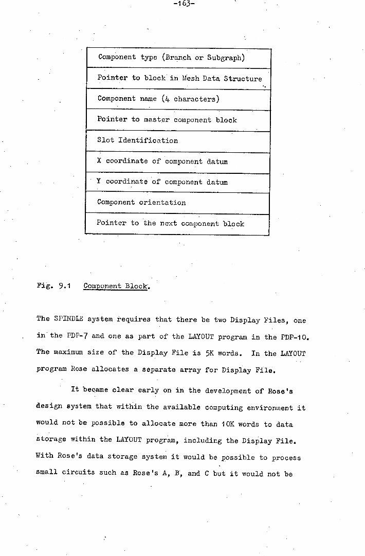
-163-
• Component type (Branch or Subgraph)
Pointer to block in Mesh Data Structure
Component name (ii. characters)
Pointer to master component block
Slot Identification
X coordinate of component datum
Y coordinate of component datum
Component orientation
Pointer to the next component block
Fig. 9.1 Component Block.
The SPINDLE system requires that there be two Display Files, one
in the PDP-7 and one as part of the LAYOUT program in the PDP-10.
The maximum size of the Display File is 5K words. In the LAYOUT
program Rose allocates a separate array for Display File'.
It became clear early on in the development of Rose's
design system that within the available computing environment it
would not be possible to allocate more than 10K words to data
storage within the LAYOUT program, including the Display File.
With Rose's data storage system it would be possible to process
small circuits such as Rose's A, B', and C but it would not be

+3
+4.
+7
+12
-164-
possible to process larger, more realistic, circuits. A number
of steps have been taken to improve the data storage system. The
remainder of this section is a description of the most significant
improvements.
Blocks within the data structure are continually being
created and deleted. In order to re-use array space a free storage
system is required. Rose's system of free storage is illustrated
in Fig. 9.2.
STORE
Fig. 9.2. Rose's Free Storage System.
The basic approach is to 'hang' blocks which have been
returned to free store in strings according. to size. If a block
of a particular size is reciuired the array store is interrogated

-165-
to determine whether any blocks of that size have been returned.
If no such block is in the free store (e.g. there is no block of
3 elements as; in the illustration) a new block is created from that
part of the main data storage array that has not., as yet, been used.
The system tends to be efficient with respect to execution speed,
but very inefficient with respect to storage. There is no
combining of blocks that are adjacent in the array or allocation
of small blocks by splitting larger blocks. As a result a new free
storage system has been used. It was devised by A.K. Hope, and is;
described in [23]. It has a comprehensive 'garbage'collection'
facilities, and is very efficient.
The biggest storage problem derives from the requirement
for a Display File. To display all of a large circuit it is;
necessary to have the maximum of 5K allocated to Display File.
Thus, using Rose's approach 50 % of the total data storage space
would be used up by Display File. To avoid this the Display File
is paged with the Mesh Data Structure, In order to do this it
is necessary to separate the component blocks from the Mesh Data
Structure because the component blocks are used in picture
generation and when accessing the mesh. The new storage organisation
is shown in:Fig. 9.3.
Pages are transfered using binary block transfers
utilising the random access file facilities of the PDP-10 system.
Because the Mesh Data Structure, is never modified within the LAYOUT
program it is only necessary to write it onto disc once, at the
begining of a program run. Thus, if the Display File - is required
and is not in core, it is' read-in immediately. If the Mesh Data
Structure is required the Display File must first be written to disc.
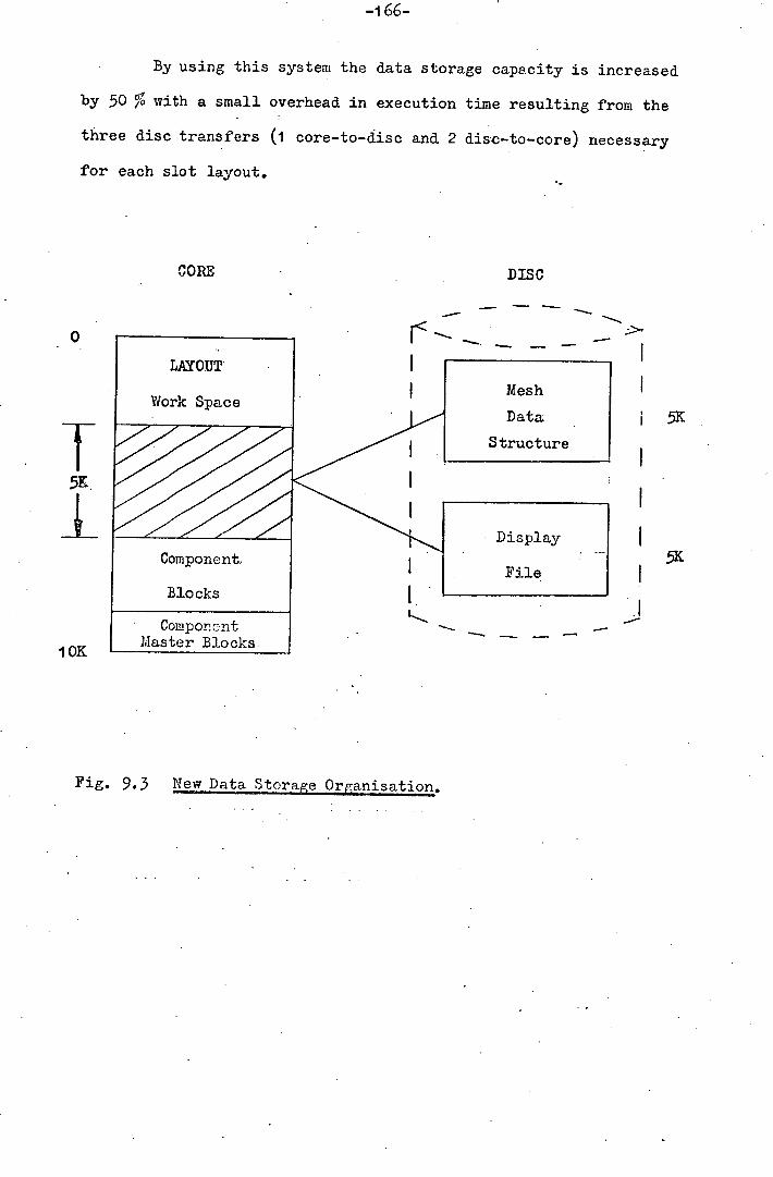
LAYOUT
Work Space
Component,
Blocks
Component Master Blocks
I
10K
-166-
By using this system the data storage capacity is increased
by 50 % with a small overhead in execution time resulting from the
three disc transfers (i core-to-disc and 2 disc-to-core) necessary
for each slot layout.
CORE DISC
- -
I Mesh
Data
I I Display I File I
5K
MI
Fig. 9.3 New Data Storage Organisation.

-167-
9.2 Layout Picture Generation.
The modified layout system is required to layout larger,
more realistic, circuits. th an Rose's system. Consequently, there
is an increased requirement for efficiency in the generation and
display of layout pictures if effective system response is to be
maintained. As a result the method of layout picture generation
has been changed.
9.2.1 Graphics Software.
Pictures of layouts are created and displayed using the
SPINDLE Interactive Graphics Package [16]. The following is a
brief description of those features of the SPINDLE system that are
pertinent to the changes in the method of picture generation.
A picture is constructed - from a number of display segments
which form a Display File. The 30 Graphics Display operates directly
on the Display File stored in the PDP-7 computer. No segment may
contain or call any other segment. A segment maybe temporarily
or permanently deleted, but it is not possible to recover display
file space allocated to segments (other than the last segment)
without complete Display File regeneration. A segment's; display -
intensity, orientation, and position may be varied without the necessity
to regenerate the Display File. -
9.2.2 Rose's Method of Layout Picture Generation.
In Rose's system each component outline, with its name,
is displayed as a single segment and all the conductors in a
layout are displayed as a single segment. Thus, the picture is
structured in in relation to the complete layout, or part layout.
A change to the picture is required when,
(i) In Unchange Mode the next slot layout is completed,
(2). in Xpress Mode the entire layout is Completed,
(3) a layout modification is required and the picture of slots
above the slot being modified is deleted.
Whenever such a change is made it is necessary to perform
the following operations,
('i) permanently delete the whole Display File,
recreate the component segments,
create a new conductor segment,
display the new picture.
Thus, when using the . Unchange Mode to conotruct a
layout the picture is completely regenerated after the layout of every
slot. This is very inefficient and slows down the overall layout
process significantly. To avoid this problem the Xpress mode of
interaction was introduced. In this mode the picture is only
regenerated when the layout is completed. This approach has two
main disadvantages,
it is not possible to complete only part of the layout,
it leads to poorer response since no change occurs to the
picture until the layout. is completed.
-169-
These disadvantages were not significant in Rose's system
because of the very simple and fast slot layout process and the fact
that only very simple circuits requiring between 10 and 20 slots
could be processed. In the modified system the slot layout process
is very much more sophisticated, and consequently slower, and the
circuits processed are much. larger requiring between 100 and 200
slots.
Another disadvantage is that it is necessary to store the
conductor routes for a large number of slots. If the picture is
produced slot-by--slot the conductors for each slot can be discarded
with a resultant saving in data storage space.
9.2.3 New Method of Layout Picture Generation.
In the new system each slot is displayed immediately after
the slot layout is completed. In the same way a complete layout is
nonstructed from a number of slot layouts, the layout picture is
constructed from a number of slot pictures.
When the LAYOUT program is initialised, a Display File is
constructed in which each component is a segment which may be
rotated, varied in intensity, temporarily removed or positioned
anywhere on the display screen.
At the start of the layout process all the components are
temporarily removed. As each slot is completed the appropriate
component segments are restored and set to the required positions
and orientations. In addition, a conductor segment is created for
the conductors of each slot,
-1 70-
This approach has the -following advantages over the previous
method,
the component segments are created only once,
as each slot layout is completed a new slot picture is
added to the existing layout picture, no regeneration is
required,
if a modification to a slot is required the slot pictures
of those slots above the slot to be modified are deleted
by temporarily removing component segments, and permanently
deleting-conductor segments. (Since the conductor segments
are the last segments generated the Display File space can
be re-used for other conductor segments),
it is not necessary at any time to store the conductors
for more than one slot,
since the layout is displayed slot-by-slot the response
is not degraded by the method of picture generation and
it is possible to stop the layout process when sufficient
slots have been completed.
9.3 Component Selection and Placement.
The basic method of component selection and placement
used in the modified system is described in. Chapter 6. The two
most important aspects of the i-rapJ..enentation are the method of
constructing combinations of components in the Selection List and
the data structure representation of components during Trial
Placement.
-171-
9.3.1 Controlling Component Combinations.
An example of the sequence in which combinations of
components from the Selection List are formed is given in Fig. 9.4.
Components from'the Working List are selected and formed into a Selection
List. A' dummy component is included to indicate the end of the
Selection List. The basis of the method of controlling the component
combinations is a software stack. A flowchart of the method of
controlling component combinations is shown in Fig. 9.5. The
components on the stack at any time represent the current component
combination under consideration.
9,3.2 Data Structure Representation of Components for Trial Placement.
The most frequent operation performed during Trial
Placement is the movement of a component within a slot. To simplify
the movement of components, each component has a Trial Placement
Block (T.P13.) associated with it. The information stored in, a T.P.B.
is shown in Fig. 9.6 and the relationship with a component is -
illustrated by Fig. 9.7.
Agreat deal of the information in a T.P.B. could be
obtained by calculation whenever it is required by reference to master
component blocks etc. Hence, execution time is being 'traded' for
data storage. This appears to be in conflict with the requirement
to make data storage more efficient. However, all the T.P.B.s
are returned to free store before the conductor routing stage.
During the conductor routing stage the conductor routes are stored
in blocks of the array. After the slot picture is generated using
the conductor blocks they are deleted. Therefore the T.P.B.s and
the conductor blocks never exist at the same time within the system.
- 172 -.
A1. A1.B1 . AB1.0
A2B1
I A2C1
A2B .0 I
Cl .
Fig. 9.4 Sequence of Component Combinations and Orientations
-1 73-
J Exit J ES
I Consider next
YES
K All combinations
element of S.L. considered ?
L after COLIP
End of S.L. End of S.L.
Orientations All orientations
to be considered remove coii
? from stack Not end
of S.L. YES
I Set up initial NO S.L. End of
I orientation Set up next orient Remove COMP
of COMP 11 1 from stack
Put component J Consider next element the stac of S.L. after COL1P
YEs
NO ientationn of COMP considered ?
er
Slot space YES next Consider
VO
TRIAL PLACLENT
Fig. 9.5 Control of Coppnent Combinations.
11
-1 7i—
The new free storage system allows the storage space used by
T.P.B.s to be used for conductor blocks.
Using the Trial Placement Blocks components may be moved
about very efficiently. When a component is moved to a new position.
all the x-coordinates for the new position may be determined by
adding a constant factor. Access to the Trial Placement and Selection
Lists is directly through pointers within the T.P.B.s.
9.4 Manual Interaction System.
The method of implementation of the new interaction system
was greatly influenced by the new component selection and placement
algorithm and the new method of picture generation.
9.4.1 Rebuilding the Layout.
When a modification to a slot is required it is necessary
to recalculate, or rebuild, the layout to obtain the Base List and
the Working List of the slot.
In Rose's system all the operations performed in the normal
layout generation process are performed. during a rebuild, i.e.
development of the Working List from the Base List,
selection and placement of components and conductor ends,
routing of conductors, -
(ii ) determination of slots,
(5) generation of the picture on completion of the rebuild.
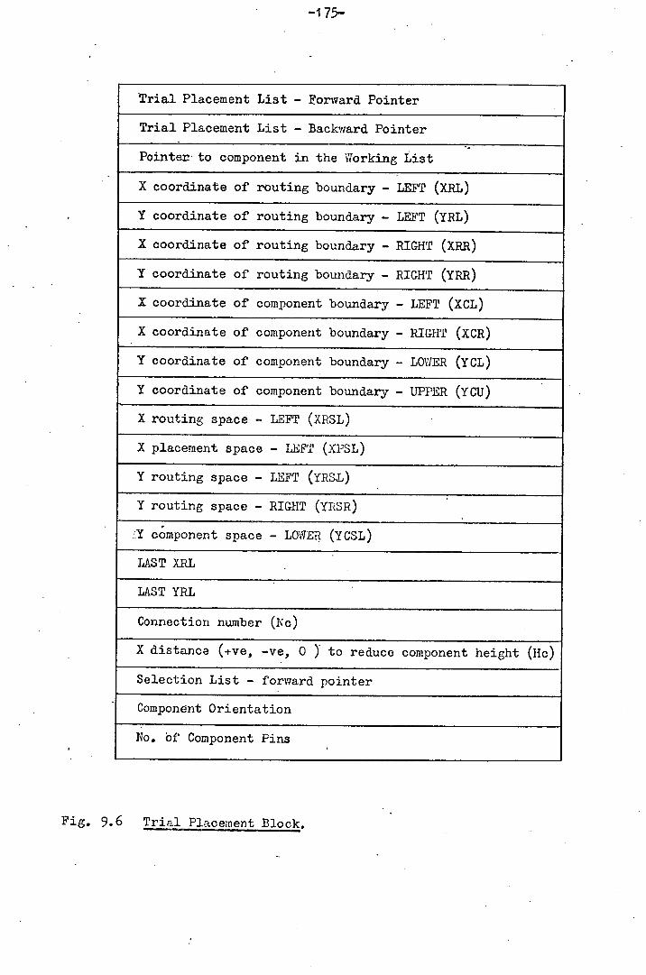
-175-
Trial Placement List - Forward Pointer
Trial Placement List - Backward Pointer
Pointer to component in the Working List
X coordinate of routing boundary - LEFT (XRL)
Y coordinate of routing boundary - LEFT (YRL)
X coordinate of routing boundary - RIGHT (XRR)
Y coordinate of routing boundary - RIGHT (YRR)
X coordinate of component boundary - LEFT (XcL)
X coordinate of component boundary - RIGHT (xcR)
Y coordinate of component boundary - LOWER (YCL)
Y coordinate of component boundary - UPPER (Ycu) X routing space - LEFT (xRSL)
X placement space - LEFT (XPSL)
Y routing space - LEFT (YRSL)
Y routing space - RIGHT (YRSR)
1:Y component space - LOWER (YCSL)
LAST XRL
LAST YRL
Connection number (Nc)
X distance (+ve, -ye, 0 ) to reduce component height (Hc)
Selection List - forward pointer
Component Orientation
No. bf Component Pins
Fig. 9.6 Trial Placement Block.

-116-
(xcR,Ycu) XCL \YCU)
I
X placement space I component
- I effective
S area
I S X routing space I
. component placement area
I . I
- - ( X CR , Y CL )•
(XRL,YRL) . S
Y Routing Space Left ( n YILIZ)
Y Routing Space Left
Y Component Space
Fig. 9.7 Component Information Stored in a Trial Placement Block.
-177-
However it is unnecessary to perform all of these operations.
The picture generation step has been eliminated as described in
Section. 9.2. In addition, the selection of components for slots
is redundant because the component positions and orientations are
known since they are stored in the component blocks. In the modified
system the selection of components for a slot is a much more
sophisticated, and consequently more time consuming, operation than
in Rose's system. It is therefore very desirable to avoid repeating
the operation when rebuilding a layout. As a result, during
rebuilding no selection of components (i.e. no Trial Placement) is
performed, and components are placed according to stored values.
9.4.2 Layout State.
The implementation of the EXIT, DATA, PLOT, COMPLETE,
CHANGE ., and DISPLAY modes is straight-forward and fairly obvious.
The D1ThP mode is used to dump layouts onto disc-:and to
subsequently reinstate layouts. The layout form is determined
completely by the positions and orientations of the components
becaus,e of the constraint that the layout correspond directly to
the mesh and the fact that no direct interaction with conductors is
permitted, Thus, to store a layout it is necessary only to store
the component positions and orientations. This information is
contained in the component blocks. Because the component blocks are
all in a contiguous part of the Store Array (Fig. 9.3) all the
component blocks may be dumped onto a file on disc in a single
binary block transfer.
9.4.3 Slot State.
The interaction modes are used to set up instructions to
the component selection and placement algorithm. Modes applicable
to unplaced components are implemented as follows,
FREE - there is no additional restriction on the orientations
at which a component may be placed,
FIX - the algorithm is constrained to placing the component
at the orientation at which it is displayed,
OMIT - the component will not be included in a Selection List
and therefore, cannot be placed,
SELECT - the only restriction on the component being included
in a Selection List is its connection number,
ORIENT - has no direct effect on the algorithm but is used to
set up a required component orientation for FIXing,
Modes applicable to placed components are implemented as
follows,
FREE - the algorithm may move the component during Trial
Placement,
DELETE - the component is made unpiaced and is OMITed,
FIX - the component becomes the boundary of a subsiot
(described below)
MOVE - the component is positioned by dragging the outline
over the display using the light pen. The component
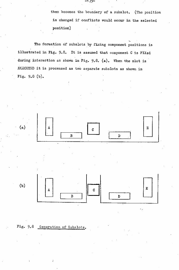
then becomes the boundary of a subsiot. (The position
is changed if conflicts would occur in the selected
position)
The formation of subs].ots by fixing component positions is
illustrated in Fig. 9.8. It is assumed that component C is FIXed
during interaction as shown in Fig. 9.8. (a). When the slot is
EXECUTED it is processed as two separate subsiots as shown in
Fig. 9.8 (b).
El E B D
(a)
(b)
Fig. 9.8 generation of Subsiots.

-1 80-
9.4.4 Display State.
All changes to the layout picture displayed are made by,
temporarily removing or changing the intensity of, component or
conductor segments. No generation of Display File is required.
0

-181,
Chapter 10. General Comments.
This chapter contains comments on the Topological Approach
to Layout Design derived from the 'theory presented in Chapter 2
and the practical experience gained from Rose's design system. In
addition, the role of manual interac.ion is discussed in general
terms.
10.1 The Significance of Graph Planarity.
A commonly proposed Topological approach is,
(i) map a circuit onto a graph,
test for planarity and extract a planar subgraph if non-planar,
transform the planar subgraph into a layout.
The basic assumption of this approach is that the planarity
of the circuit graph is the necessary and sufficient condition for
a layout without track crossings to exist. In the author's opinion
this assumption is false, for the following reasons,
(i) a conductor may be represented in a layout by a wire juniper.
Thus it is not necessary for a graph to be planar for a
Valid layout to exist,
(2) a conductor may be routed between the pins of a component.
Depending on the circuit/graph mapping this means either,
(a) a non-planar graph may be transformed into a valid layout,
as with Rose's mapping,
-1 :i-
or, (b) a graph may be changed to make it planar, as with
Basden and Nicholls mapping.
(3) The orientation of the pins of a component is generally fixed.
This means that the conductor tracks must be routed to a
component in the correct sequence to avoid track crossings.
(In general the possibility of routing conductors between
pins provides only limited flexibility in the sequence)
Thus, it is possible for a graph to be planar and yet
not be realisable as a valid layout.
It may be concluded from the above that the planarity of a
graph is neither a necessary or sufficient condition for a valid
layout to exist. In fact, because of the possibility of routing
conductors between component pins the problem becomes one of synthesis
and not of analysis. The problem with constructing a graph is that
it does not define the topology of a layout viz, it does not define
the regions of an embedding or the orientation of edges incident
at a node. A far more useful circuit representation is a mesh, since
in addition to describing connectivity it can also define the regions
of an embedding.
10.2 The Mesh Layout Relationship,
The most common Topological approach that is implemented
consists of the following operations,
(i) map the circuit onto a graph,
(2) construct a mesh,
-183-
(3) Transform the mesh into a layout.
Using this appràach the topology of a layout is defined
prior to the consideration of any topographical layout information.
(E.g. component geometries, conductor tracks etc.) and unnecessary
conductor crossings are avoided. Thus the topological layout
constraints are satisfied. However, the topographical layout
constraints must also be satisfied (E.g. packing density, electrical
constraints, thermal constraints, as described in detail in Chapter 4.)
If the form of the mesh had no appreciable effect on the form of
the corresponding layouts, topological and topographical constraints
could be satisfied separately without limiting the layout
capability. Unfortunately this is not the case. Experience of
interaction with layouts which are topologically constrained by a
mesh has shown that the form of the mesh very severely restricts
the form of the corresponding layout. Thus, the satisfaction of
topographic constraints is, in general, inhibited by the form of
the mesh.
Because of the possibility of routing conductors between
the pins of components, there are, in general, a large number of
meshes which satisfy the topological layout constraints for a given
circuit. It is therefore possible (in theory at least), to obtain
a layout solution by constructing a mesh which does not inhibit
the satisfaction of the topographic layout constraints. The problem
lies in obtaining a 'good' mesh with respect to a set of topographic
layout constraints. As shown in Chapter 4. the topographic layout
constraints are not, in general, well defined, and can only be
effectively satisfied viii;h the aid of manual interaction. It may

be deduced that it is essential that manual interaction allows
changes to be made to the mesh. Since the topographic layout
constraints relate to the form of the layout, and not to the form
of the mesh, it is only sensible that interaction be performed with
the layout and not with the mesh. Indeed it is very desirable that
the mesh be invisible to a system user. Thus the user should modify
the layout and the system should automatically update the corresponding
mesh, if necessary.
Using this approach the layout appears to be 'driving' the
mesh rather than the reverse, as initially proposed. The question
that therefore arises is - 'Why have a mesh at all ? 7hy not just
store the layout form ( the topography) and interact directly with
that?' In fact in any approach which stores the form of a layout
the information which constitutes the corresponding mesh for any
given circuit mapping is also stored. Thus, the question really
is 'What justification is there for haying an additional structure
containing only topological informatioñ - - -
In the author's opinion a mesh can prove very useful for
the following reasons,
(1) in a large,-complex, layout it is very easy for a user to
construct partial layouts which do not represent the basis
of topological solutions. As shown with Rose's system a
mesh may be used to obtain a complete layout which satisfies
the topological layout constraints. A layout produced in
this way may be used as the starting point for manual
interaction s -
-185-
during interaction a mesh may be used to allow only layout
modifications which satisfy the topological layout constraints,
limited topological analysis-may be performed to improve
the layout form automatically e.g. by rerouting conductors.
10.3. The Bole of Interaction.
Manual interaction is frequently incorporated in layout
design systems to compensate for the inadequacies of the automatic
layout algorithm used. If it is acceptedthat there isa need-for
interaction ( as argued in Chapter i) there would appear to be a
case for considering its use at the initial system design stage.
In order to obtain a system which fully utilises the capabilities
of both man and machine in an efficient manner it is necessary to
establish their relative capabilities with respect to the layout
design problem.
Perhaps the man's most significant capability is that of
pattern recognition. He. can see at a glance what is wrong with a
layout, and work out strategies for improvement involving whole
groups of components and conductors quite easily. A machine is
'blind'. It has to'feel' its way around a data structure, representing
a layout, inorder to obtain any kind of pictorial information.
In addition, it is very difficult, if not impossible, for a machine
to analyse such information in order to make sensible decisions
relating to groups of components and conductors. Thus, the man's
most important capabilities are considered to be pattern
recognition and the ability to generate strategies for layout
improvement.

-186-
The machine's most significant capability is its ability to
'remember' large amounts of detailed information e.g. the
connections of a circuit, the dimensions of all the components
in a circuit etc. In addition, it can perform well defined
calculations very efficiently and present the results of such
calculations in a variety of forms very quickly.
The general system strategy that is suggested by this
(admittedly very simple) analysis is basically 'Let the manmake
the decisions and the machine do the housekeeping'. Using this
approach the machine's role is that of aiding the man rather than
the reverse, as is commonly the case, and there is a greater
probability that an effective symbiosis of man and machine will be
achieved.
-187-
Chapter 11. Conclusions.
It is not considered that the Modified Design System,
developed from Rose's Design System, is suitable for industrial use.
However, the layouts of practical circuits obtained using the Modified
Design System show that the use of the Topological Approach to design
single-sided printed circuit board layouts is justified.
Manual Interaction has an essential role to play in any
general layout design system for the solution of practical layout
problems. Interaction is frequently incorporated in design systems
to 'patch-up' deficiencies in automatic layout algorithms. In the
author's opinion it is essential that the role of interaction be
considered in detail at the initial system design stage - if an effective
symbiosis of man and machine is to be achieved.
Experience with Rose's system has shown that the form of the
mesh of a circuit can severely restrict the form of the corresponding
layouts. It is therefore considered essential that the interaction
allows changes to be made to the mesh.
Existing layout design systems in general fall into two
broad categories,
those that concentrate on the satisfaction of topological
layout constraints,
those that concentrate on the satisfaction of topographical
layout constraints.

In the author's opinion the most desirable approach viould
be to place equal emphasis on the satisfaction of both topological
and topographical layout constraints.

Acknowledgements.
The research work for this thesis was carried out in the
Computer Aided Design Project of the Department of Computer Science
of the University of Edinburgh.
I would like to thank the various members of the Computer
Aided Design Project who have helped me in my research, and in
particular I should like to thank Dr. J.V.Oldfield who supervised
the work.
In addition my thanks are due to British Aircraft Corporation
(Stevenage) for seconding me to the University for the duration of
the research.
The computing facilities were provided by the U.K. Science
Research Council under grant Ref. B / SR / 88746.
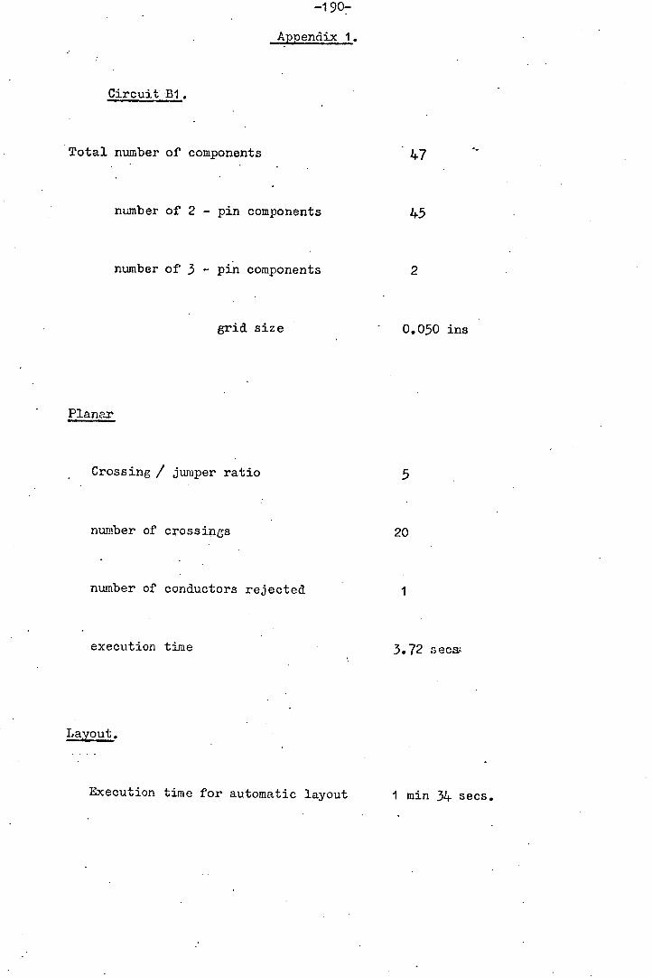
-190-
Appendix 1.
Circuit LI.
Total number of components
number of 2 - pin components
number of 3 - pin components
grid size
47
if 5
2
- 0.050 ins
Planar
Crossing / juniper ratio
number of crossings
number of conductors rejected
execution time
5
20
I
3.72 seca
Layout.
Execution time for automatic layout 1 min 34 secs.
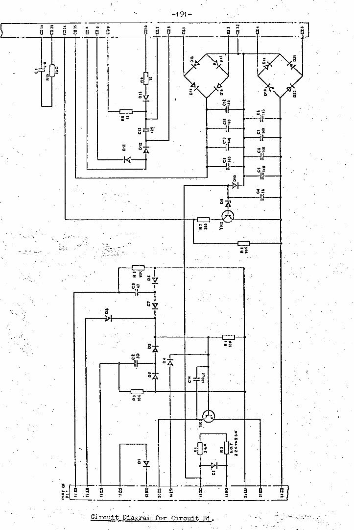
-191-
_ —HF--
f4
cc A
It cc 9
U .
a
.>1. .
.. . .
• . • . •
.•
edo -
CL
tfl
le
c 112
V. it
Circuit Diaji for Circuit 131.
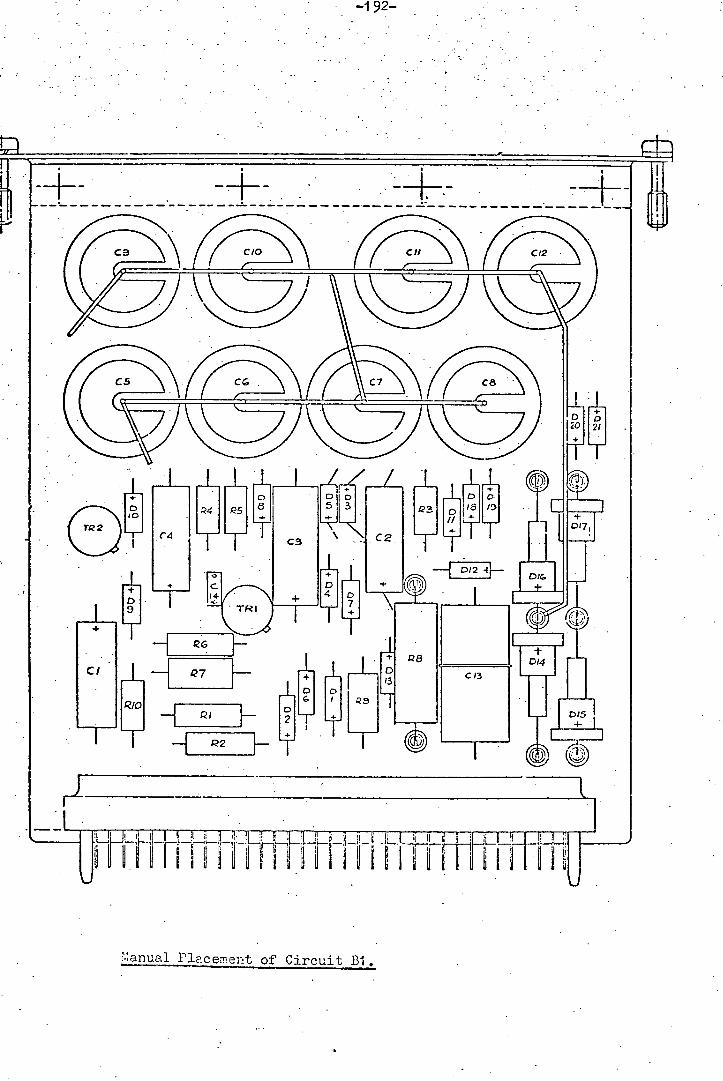
4'
0
LJ
Io I U
C3 r4 TT
IL + _
r1
iI 9T RI
I' I ° T Li
ftrmiTrnhiTrft I fi
anua1 Placement of Circuit BI.
I
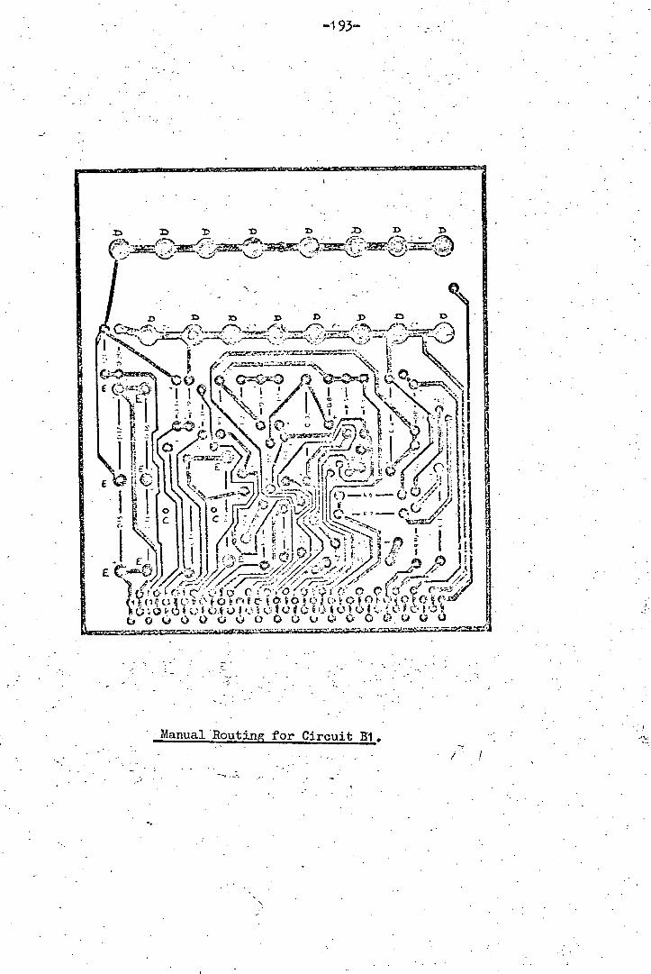
-193-
ly
-
if
Y >Y(!
L \-II-.• - I •- ;f )_¼. 06
E C >-k1
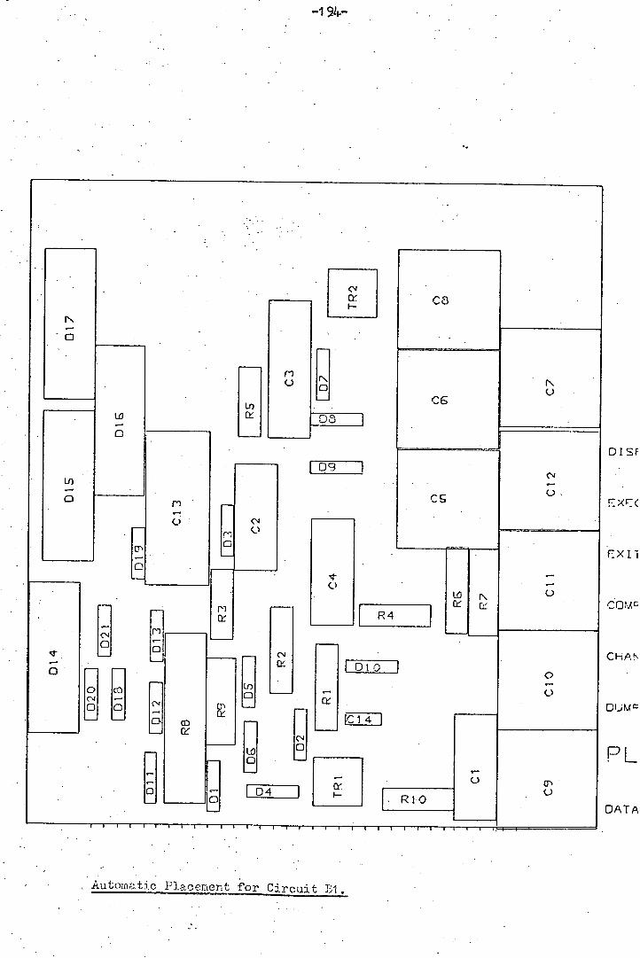
DISF
EX f (
EXI1
COM c
C H A P\
Dl-
L
;Mr-P
DATA
-194—
Autornat,c Placement for Circuit LI.
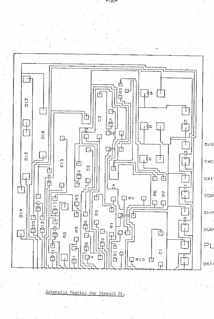
—i1-
RIO
8
•L1
Ld N.
G
LII
El ff
IHL Ln Wj
R
Automatic Rout± , for Circuit BI.
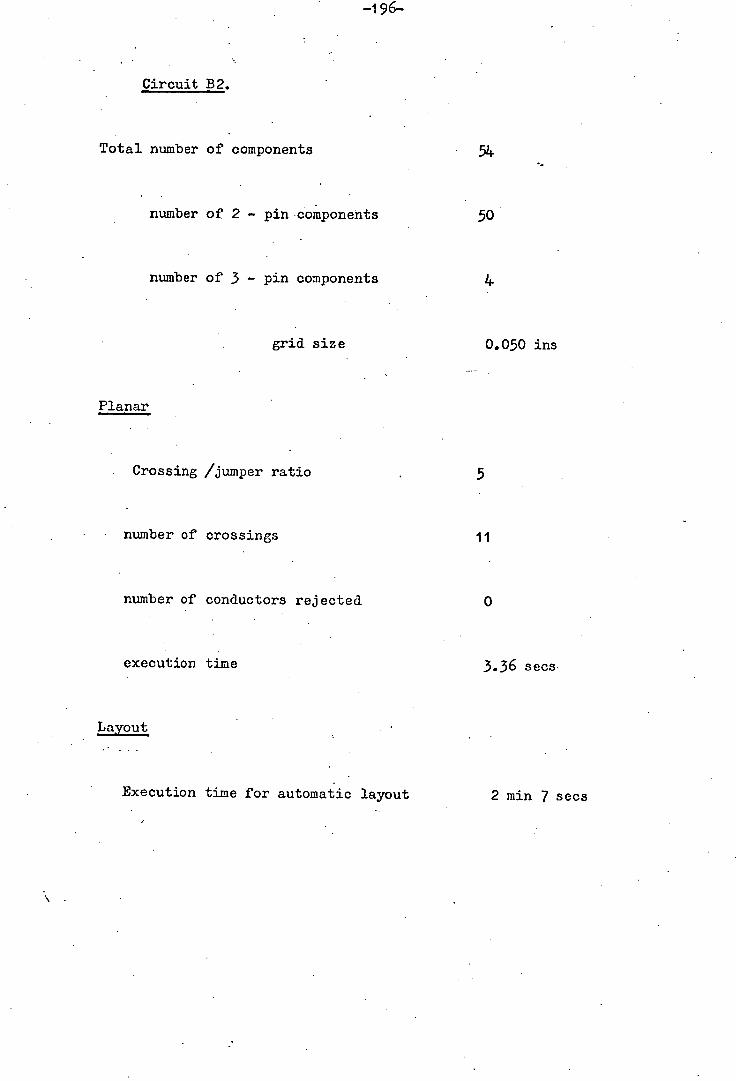
-196—
Circuit B2.
Total number of components 5z
number of 2 - pin components 50
number of 3 - pin components 4
grid size 0.050 ins
Planar
Crossing /jumper ratio
number of crossings
number of conductors rejected
execution time
• 5
11
0
3.36 secs
Layout
Execution time for automatic layout 2 min 7 secs
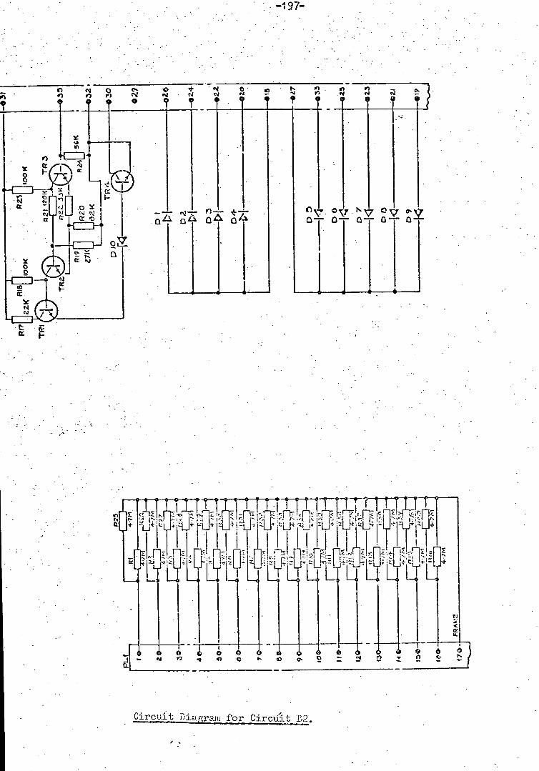
74 , 71; ~z
ZAU
rj .. r. Fil 1LLfL ?iTi11iüii' LA1r1T
L
Circuit Diairam for CircutB2.
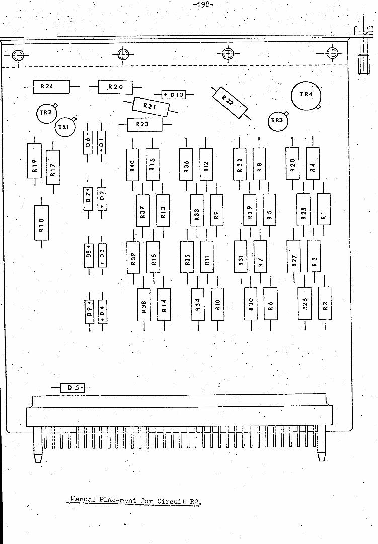
TLIIF -rm --- 14
TRI R23
• •.L:_J ; •I,II [C2 C.0
2 ce Lc, 0: ed w w
I JT L-r LF
E1
• • •
I MflHdflijtdii1tifftUflfl1
Manual Place m ent for Circuit B2
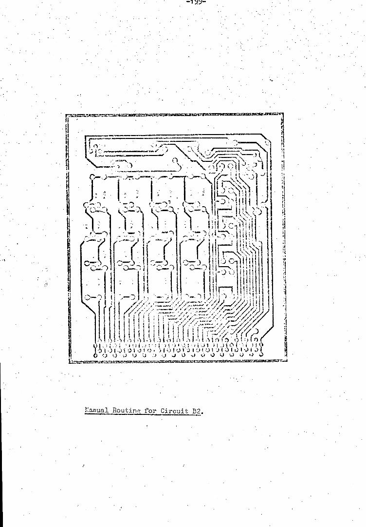
2__ i3Ti '1
2c1 JILY)
_ ---- _-, J l •---) .-.', i I -
Z 11L111I!i'iI1 I l
1!r1 11' 1t
I )IjZ'1
Manual Routing for Circuit B2.
/

-200-
Clq TR
M F2]
RIS I
R 31
Of 0
Cff CN Of C4
Automatic Placement for Circuit B2.
Nr
0 CN
CN
IH [s1
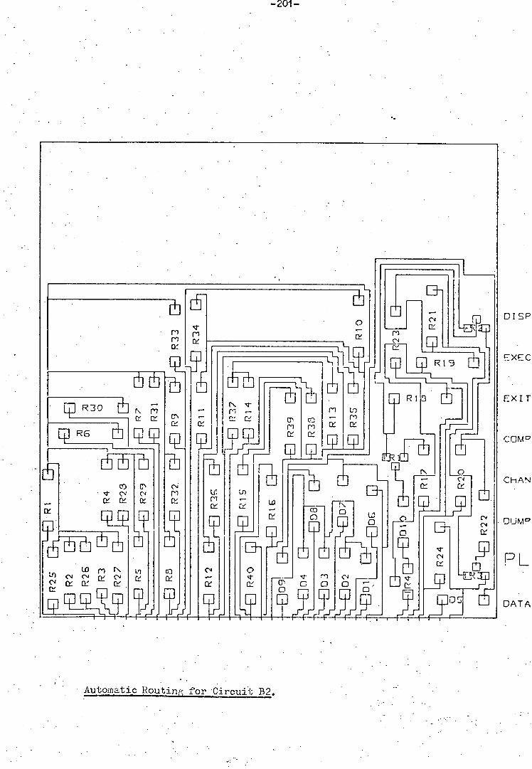
(N (N
-201-
•
•1H
•____ llhThdj
R3QJ
LC
U) - • C,' • cr (14 of af Of (3 C 0 0
__ _____
• • •. Automatic Routing for Circuit B2.

-202-
Circuit B3.
Total number of components 52
number of 2 - pin components 45
number of 3 - pin components 7
grid, size 0.050 ins
Planar
Crossing /jumper ratio 5
number of crossings 27
number of conductors rejected 3
execution time 7.64. sees
Layout
Execution time for automatic layout I ruin 18 sees
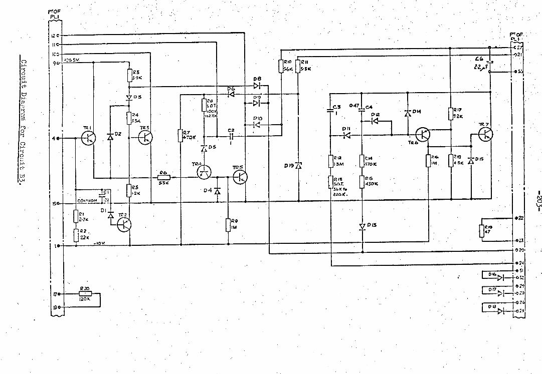
PTOF :.
P .
.J.
I
-J.

1
_________________________ I _________________________ • •
_ EiIF
IL 1=1 1 L • • L_J U U F1Ffl • • • I Li—.
ri i I •
I 1 T
IJ I J —I I • •
UM I -EIIL1-- ffF
nT R
n4 Id L1Jth1T .11:
iLrii; .i. •-- I • • • co
-j- •
-___H
In Placement for Circuit B3.
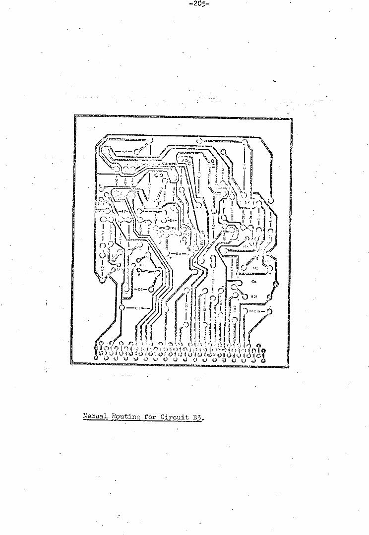
-25-.
\\ ;\\j
)tC. \\\ • iI i ' f& f I I
I-) ii! I LJAJ
U.: ..-i I :\'\)-- •i//•
. I.) U •)4j
Manual Routjnr for Circuit 133.
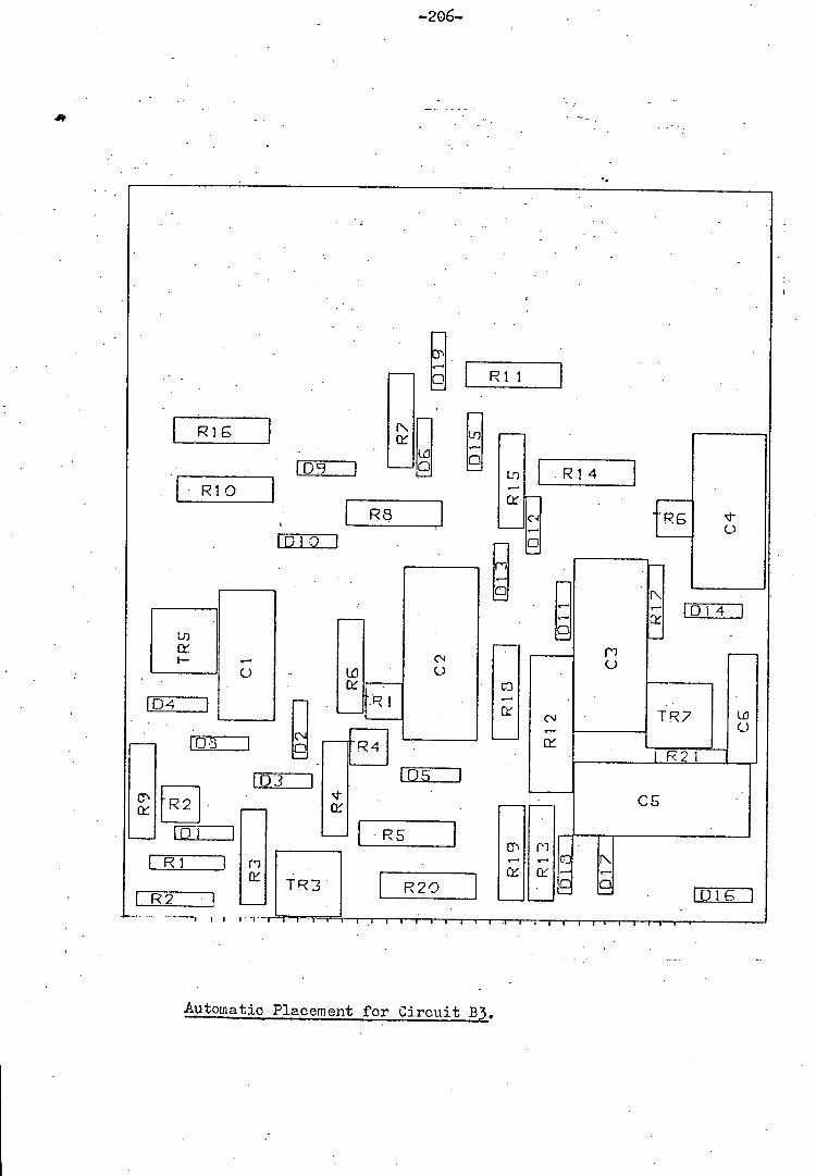
-206-
LR11 I
R G
LO .R14 [Rio
LR81 L1 fE
LO
III
'1 [Qj4 01 I C j
L Iwl 0
LI R 4
21
T R 7
[R 2]
D3 0S1
iIL1 LR2O HH LD11
___1 I I I I I • I I I I I I I •1 - I I I 1 I
Automatic Placement for Circuit B3.
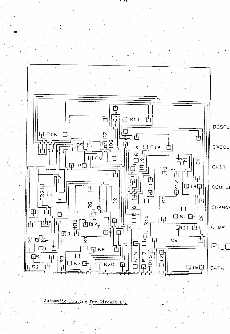
II OISFL
9. 1 EXCU
- '-V t
I EXIT
DLr --j H
4 _
42 fj R5 '1 YR I El
LY E~7 [y
14
CID EJ Ep _-T
EE I E~
El- cs
COMPL
C H A NC
J U M P
PLC
DATA
Automatic Routing for Circu

-208-
Circuit Blf
Total number of components
number of 2 - pin components
number of 3 - pin components
number of 6 - pin components
grid size
63
43
16
if
0.050 ins
Planar
Crossing / jumper ratio 5
number of crossings 37
number of conductors rejected 13
execution time 21.26 secs
Layout
Execution time for automatic layout I min 40 sees
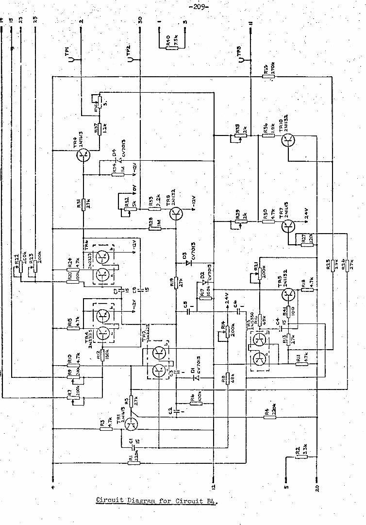
&
'I
+ >
I •
0 •.
• tr
09
01
on CO
CC Ci on
cc z
-; • - -
-M- I
In R Sk -r - jCl
'2 c Cq
cc
r In
cc Q In
r4 0
M •
T"YOO
CO L T-J~= OD
Cr
rl
• _____-
'I- • • • • to
• • Circuit Diagram for Circuit B4 . • •,
R 3cil
2-77 Rl.
Oil) .
A
:(otpi
T R7 RBJ J I •1 JR1
• fl R2.9 • L1i • y •
cl C2. L1i Ii •
R35
ri i~
+T E DI
C3 15
C7 E LI • R
•8 9 . _f ... C5
F •. 19 LIR21
• . . • [j . S 9 -55 S ____F
II
I . .. . .1 .
I I Ri
1rnua1 Placement for Circuit 131;..
—211-
-S.. .5
S S4
© Q p ' e s— 4
2 2 C 1iCzC c. Cl ;
? i
-i ------ I
I
_Ii
1° —D
Cr -,
' .5)
4 .: =J -- •. .
!-j
(I 7P~~—
•Sj i !t7 !
o
CA I
/ 1 • •. _____ o•• 1 7 -I 'F .i• i
iva outin for Circuit B1-.
-212-
• H . LL2--J
CCI
•.IoI _
LJ . flrRT
ii
T19 -
[Y C LO
L JU ry
oUiI2IJ
rca R32 I
TR33 ri fl LE2 [c1 R 22 [ R23
-----------rTrr-r-r i rvr rir- riTTTr
ft
DISPLAY
I EXECUTE
I EXIT
I COMPLETE
I CHANCE
I DUMP
PLOT
I DATA
Automatic Placement for Circuit B
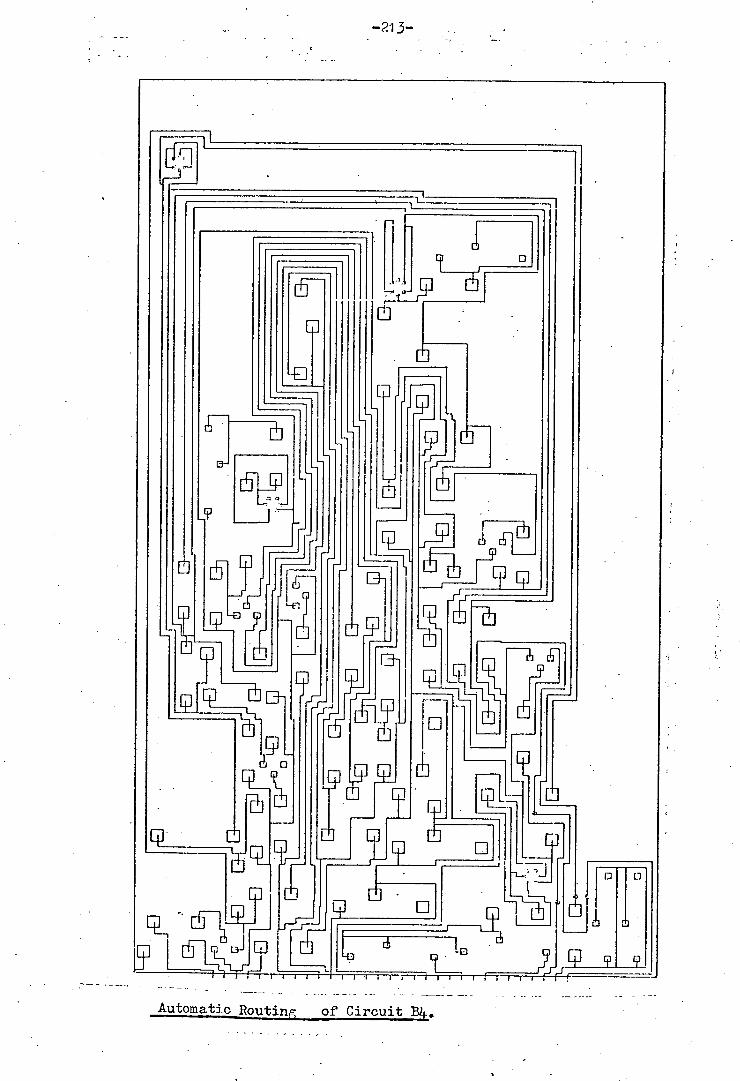
- —213—
pr=;-
13
Hill FR If/-FFF
jR7~rll~
Y IIIF
ED
EilUIIIIU
D
Automatic Routing of Circuit P4.
- 213-
- REFERENCES.
(i) Narraway, J. J.,. 'Untangling a graph with C.A. D. and P. C.B.
applications.t. Internal Technical Note ST 5970 (May '71)
British Aircraft Corporation, Stevenage, Herts.
Narraway, J.J., 'Component Orientation in P.C.B. Layouts'
Internal Technical Note ST 6027 (July 171) British Aircraft
Corporation, Stevenage, Herts.
Narraway, J.J., 'Component Distribution in P.C.B. Layouts'
Internal Technical Note ST 614.7 (August '71) British
Aircraft Corporation, Stevenage, Herts.
(i) Bader, 1U., 'Topological Problem of Printed Circuits and its
Solution.' Archiv FUr Electrotechnik Vol. 4.9, No 1,
p2 - 12, 1 964.
Kodres, U.L,, 'Formulation and solution of circuit card design
problems through use of graph methods', in 'Advances in Electronics
Circuits Packing' Vol 2, New York, Plenum 1962 pp 121 - 14.2.
Nicholson, T.A.J., 'Permutation procedure for minimising the
number of crossings in a network'. Proc. I.E.E. Vol. 115,
No. 1 January 1968.
Fletcher, A.J. J. 'EUREKA-.— A system for laying out circuits
using a single layer of interconnections.' I.E.E. Conference
Publication No. 86 31 C.A.D. 1972., pp 187 193.
-214-
Engi, W.L.,, and Mylnski, D.A., 'Topological Theory of
Integrated Circuits', Paper from N.A.T.O. Seminar,
Bournemouth, England, 1972.
Engi, W.L., and Mylinski, D.A., 'Embedding a graph in a
plane with certain constraints'. I.E.E.E. Trans CT - 17,
No 2 May 1970, pp 250 - 252.
(io) Goldstein, A.J., and Schweikert, D•G• ; 'A Proper Mode]. for
Testing the Planarity of Electrical Circuits', The Bell
System Technical Journal, Vol. 52, No 1, January 1973.
Shirey, LW., 'Implementation and Analysis of Efficient Graph
Planarity ...' Ph. D. Thesis, 1969, University of Wisconsin,
- Mathematics.
Basden, A., and. Iichols, KG-., 'New topological method for
laying out printed circuits, Proc. I.E.E. on Circuit Theory
Paper 6894.E, March 1973.
Rose, LA., 'Computer Aided Design of Printed Wiring -
Boards'. Ph. D. Thesis, April 1970. Faculty of Science,
Edinburgh University.
(14.) Ore, O.J. 'The Four-Color Problem'-, Academic Press, 1967.
(15) Miller, R.B., 'Response time in man-computer conversational
transactions.' Proc. of the Fall Joint Conference pp 267 - 277.

- 215 -
(16) Kilgour, A.C., 'SPINDLE - An Interactive Graphics Package
for a PDP-1 0 linked with PDP-7 and 340 display.' Users;
Manual, 1973, C.A.D. Project, Department of Computer Science
Edinburgh University.
('1 7) Tarjan, R.E. , 'An Efficient Planarity Algorithm.' - Stanford
University Report, STAB-CS-244-71, November 1971.
(16) Goldstein, A.J., 'An Efficient and Constructive Algorithm
for Testing whether a Graph can be Lnbedd,edin a Plane', Graph
and Combinatorics' Conference, Office f Naval. Res. Logistics
Proj., Contract No. NONR 1858-(21). Dept.. of Math.,
Princeton University (May 16 -18, 1963).
(19) Fisher, G.J. and Wing, 0., 'Computer Recognition and Extraction
otPianar Graphs from the Incidence Matrix'. I.E.E.E.
Transactions on Circuit Theory, Vol CT-13, No 2, June 1966
pp154--163.
('20) Hóperoft, J., and Tarjan, R., 'Planarity Testing in V log V
Steps: Extended Abstract', Stanford University, Stanford,
California.
Tutte, W.T., 'How to Draw a Graph'. Proc. London Mathematics
Society, Vol. 13, (1963) pp 713 - 768.
Tutte, W.T., 'A Theorem on Planar Graphs', Trans Amer. Math.
Soc., Vol. 82, May 1956, pp 99 - 116.

- 216 -
(23) Hope, A.K., 'The Application of Interactive Computer
Techniques and Graph-Theoretic }Aethods to Printed Wiring Board
Design', Ph, D, Thesis, 1973, Faculty of Sciehee, Edinburgh
University.

- 217 -
Declaration.
I declare that this thesis was composed by myself and that
the research work described was performed by myself unless specifically
stated otherwise within the text.
(T. Cadman)
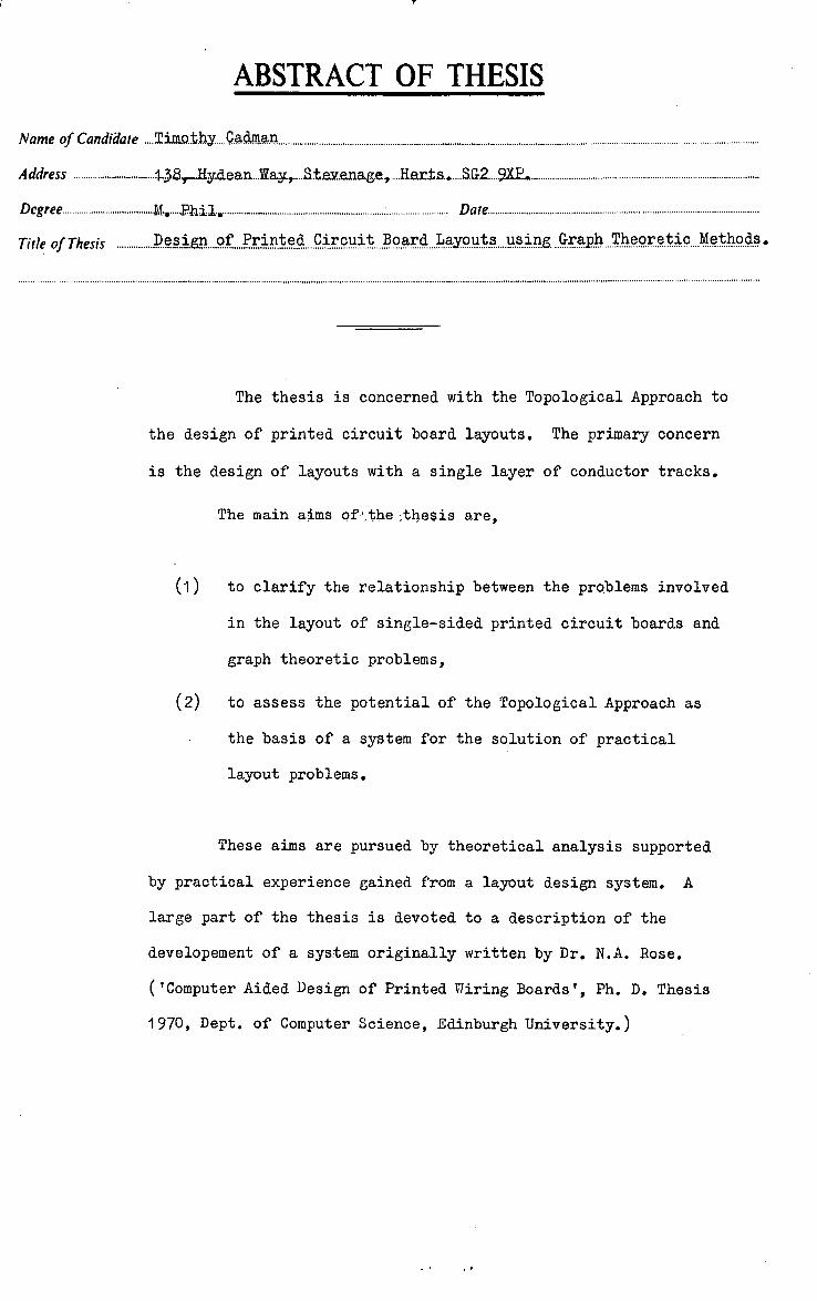
ABSTRACT OF THESIS
Name of Candidate
Address ................
Degree .................................... ... ........... ................................................................................... Date ................................................................ .................................................
Title of Thesis ............... .of Circuitoadyoitsuing. GraphThretic....MethOd.s.
The thesis is concerned with the Topological Approach to
the design of printed circuit board layouts. The primary concern
is the design of layouts with a single layer of conductor tracks.
The main aims of'.the ;tIesis are,
(i) to clarify the relationship between the problems involved
in the layout of single-sided printed circuit boards and
graph theoretic problems,
(2) to assess the potential of the Topological Approach as
the basis of a system for the solution of practical
layout problems.
These aims are pursued by theoretical analysis supported
by practical experience gained from a layout design system. A
large part of the thesis is devoted to a description of the
developement of a system originally written by Dr. N.A. Rose.
('Computer Aided Design of Printed Wiring Boards', Ph. D. Thesis
1970, Dept. of Computer Science, Edinburgh University.)