design of operational amplifier for pipelined analog to ... · agarwal for her help and suggestions...
TRANSCRIPT

Design of Operational Amplifier for Pipelined
Analog to Digital Converter
A thesis submitted in partial fulfillment of the
requirement for the award of degree of
Master of Technology in
VLSI Design & CAD
Submitted By
Sunny
Regn. No. 600961026
Under the Supervision of
Ms. Megha Agrawal Dr. Alpana Agarwal
Project Faculty Associate Professor
Department of Electronics & Communication Engineering
Thapar University
Patiala-147004, INDIA
July- 2011

i

ii
ACKNOWLEDGEMENT
With a deep sense of gratitude, I wish to express my sincere thanks to my supervisor, Dr.
Alpana Agarwal, for her immense help in planning and executing the work. The confidence
and dynamism with which she guided the work requires no elaboration. The company and
assurance she provided, has been very much valuable to me and I may hope same kind of
affection and guidance from her in the future also. Her valuable suggestions during the
course of work are greatly acknowledged. I also want to thank my co- supervisor, Ms. Megha
Agarwal for her help and suggestions during the thesis work.
My sincere thanks are due to Prof. A. K. Chatterjee, Head of the Department, for providing
me constant encouragement. Special thanks are due to Mr. B. K. Hemant and Mrs. Manu
Bansal Mam for extending timely help. The cooperation I received from other faculty
members of this department is gratefully acknowledged. I will be failing in my duty if I do
not mention the laboratory staff and administrative staff of this department for their timely
help.
I want to thank my friends specially Mr. Anil Singh and Wazir Singh. I also want to thank
my parents, who taught me the value of hard work by their own example. I would like to
share this moment of happiness with my father, mother and brother. They rendered me
enormous support during the whole tenure of my thesis work.
Finally, I would like to thank all whose direct and indirect support helped me during my
thesis work.
Date : SUNNY
iii
ABSTRACT
This work presents the design of operational amplifier in UMC 0.18µm technology using
Cadence tool. The circuit is to be used in pipelined Analog to Digital Converter. Operational
amplifier plays an important role in designing the ADC because it is the op amp which
decides the conversion rate and power consumption of complete ADC. A single ended or
fully differential op amp can be used in the multiplying digital analog converter (MDAC)
unit. It is the architecture of the ADC which decides which op amp is to be used in it. In this
specific application of ADC which is 8-bits pipelined ADC with 1-bit per stage architecture,
there was a need of two different op amps. One was required for the basic MDAC unit and
other for the unity gain configuration.
Both op amps have been designed for the specific application. The specifications of both op
amps were decided after studying the complete architecture of ADC. Four types of op amps
i.e simple two stage, telescopic, folded cascode and gain boosted architectures have been
studied and designed step by step in this thesis.
Simple two stage and telescopic amplifier have been implemented in single ended as well
fully differential configuration. Folded cascode and folded cascode with gain boosted
technique have been designed in fully differential configuration. The designs with best
performance of gain, UGB, power and settling time have been used in the pipelined ADC as
final designs.

iv
TABLE OF CONTENTS Page No. DECLARATION i
ACKNOWLEDGEMENTS ii
ABSTRACT iii
TABLE OF CONTENTS iv
LIST OF FIGURES vii
LIST OF TABLES ix
ABBREVIATIONS x
ORGANIZATION OF THESIS REPORT xi
CHAPTER 1 INTRODUCTION AND DESIGN MOTIVATION 1 1.1 BACKGROUND 1
1.2 NEED OF FULLY DIFFERENTIAL AMPLIFIER 2
1.3 MOTIVATION 3
CHAPTER 2 LITERATURE SURVEY 10
2.1 OPERATIONAL TRANSCONDUCTANCE AMPLIFIERS 13
2.2 BASIC FUNDAMENTALS OF DIFFERENTIAL OPAMP 14
2.3 ADVANTAGE OF DIFFERENTIAL OUTPUT OP-AMP 16
2.4 OPERATIONAL AMPLIFIER COMPENSATION TECHNIQUES
2.5 COMMON MODE FEEDBACK 19
2.5.1 PRIMARY REASON FOR COMMON MODE FEEDBACK 19
2.6 SIMULATION METHODS 22
2.6.1 AC ANALYSIS 22
2.6.2 CMRR MESUREMENT 23
2.6.3 PSRR MEASUREMENT 23
2.6.4 ICMR MEASUREMENT 24
2.6.5 SLEW RATE MEASUREMENT 24
2.6.6 TRANSIENT ANALYSIS 24

v
CHAPTER 3 DESIGN OF SIMPLE TWO STAGE AND TELESCOPIC AMPLIFIER 25 3.1 DESIGN OF SIMPLE TWO STAGE OP AMP 25
3.2 DESIGN PROCEDURE OF SIMPLE TWO STAGE OP AMP 30
3.3 SIMULATION RESULTS. 31
3.3.1 SIMULATION RESULTS OF SINGLE ENDED SIMPLE TWO STAGE OP AMP 32
3.3.2 SIMULATON RESULTS OF FULLY DIFFERENTIAL SIMPLE TWO STAGE OP AMP 34
3.4 TELESCOPIC OP-AMP DESIGN 37 3.5 DESIGN OF FIRST STAGE OF TELESCOPIC OP AMP 39
3.6 DESIGN OF TWO STAGE FULLY DIFFERENTIAL TELESCOPIC OP AMP 41 3.7 DESIGN PROCEDURE FOR TELESCOPIC OP AMP 43
3.8 SIMULATION RESULTS 45
3.8.1 SIMALTION RESULTS OF SINGLE ENDED TELESCOPIC OP AMP 46
3.8.2 SIMULATION RESULTS OF FULLY DIFFERENTIAL TWO STAGE OP AMP 48
CHAPTER 4 DESIGN OF FOLDED CASCODE FULLY DIFFERENTIAL AMPLIFIER 51
4.1 BASIC FOLDING CONCEPT 51
4.2 DESIGN PROCEDURE FOR FOLDED CASCODE OP AMP 54
4.3 SIMULATION RESULTS FOR FOLDED CASCODE. 57
4.4 INTRODUCTION TO GAIN BOOSTIING 59
4.5 DESIGN PROCEDURE OF GAIN BOOSTED OP AMP 62
4.6 FULLY DIFFERENTIAL FOLDED CASCODE OP-AMP WITH GAIN BOOSTING 64
AMPLIFIERS
4.7 LOW VOLTAGE HIGH OUTPUT IMPEDANCE CONSTANT CURRENT SOURCE 65
4.8 SIMULATION RESULTS FOR GAIN BOOSTED FOLDED CASCODE. 67
CHAPTER 5
LAYOUTS AND POST- LAYOUT SIMULATION 70
5.1 ISSUES IN ANALOG LAYOUT 71
5.1.1 MATCHING OF DEVICES 71
5.1.2 NOISE ISSUE IN LAYOUT DESIGN 74

vi
5.2 LAYOUT DESIGNS WITH LVS MATCHED 75
5.2.1 LAYOUT OF SINGLE ENDED SIMPLE TWO STAGE OP AMP 75
5.2.2 LAYOUT OF FULLY DIFFERENTIAL SIMPLE TWO STAGE OP AMP 76
5.2.3 LAYOUT OF SINGLE ENDED TELESCOPIC OP AMP 76
5.2.4 TELESCOPIC FULLY DIFFERENTIAL OP AMP 77
5.2.5 FOLDED CASCODE FULLY DIFFERENTIAL OP AMP 77
5.2.6 PARASITIC EXTRACTED VIEW (R & C) 78
5.2.7 ZOOM-IN VIEW OF PARASITIC EXTRACTED LAYOUT 78
5.3 POST LAYOUT RESULTS AT tt CORNERS 79
CHAPTER 6 82
CONCLUSION AND FUTURE SCOPE 82
APPENDIX A 84
REFERENCES 85
vii
LIST OF FIGURES
Fig. 1.1 1 bit per stage 10 bit pipelined ADC
Fig. 1.2 Basic MDAC unit of a 1 bit per stage pipelined ADC
Fig. 1.3 Single stage of 1- bit architecture of pipelined ADC.
Fig. 2.1 Settling Time
Fig. 2.2 Schematic Symbol of an OTA.
Fig. 2.4 Input/ Output of balanced fully differential op amp
Fig. 2.5 Differential input signal and differential output signal
Fig. 2.6 Symbol of fully differential op amp
Fig. 2.7 Illustration of output common mode
Fig. 2.8 Simple two stage operational amplifier
Fig. 2.9 Nulling resistor compensation block
Fig. 2.10 Current mismatch problem
Fig. 2.11 Fully differential amplifier with CMFB
Fig. 2.12 Setup for AC analysis
Fig. 2.13 Setup for CMRR measurement
Fig. 2.14 Setup for PSRR measurement
Fig. 2.15 Setup for ICMR measurement
Fig. 2.16 Setup for slew rate measurement
Fig. 2.17 Setup for transient analysis
Fig. 3.1 Block Diagram of basic Op-amp
Fig. 3.2 A classic Two Stage Op-amp Architecture
Fig. 3.3 Schematic of Fully Differential Two Stages OTA
Fig. 3.4 Small signal equivalent of two stage OTA
Fig. 3.5 Single ended and Fully Differential Single Stage Telescopic op-amp
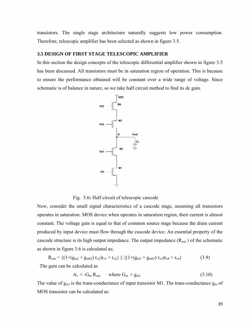
Fig. 3.6 Half circuit of telescopic cascode
Fig. 3.7 Fully Differential Telescopic Operational Amplifier
Fig. 4.1 Basic Folding Concept
Fig. 4.2 Fully differential folded cascode amplifier
viii
Fig. 4.3 Fully Differential Folded Cascode Amplifier
Fig. 4.4 Basic Gain Boosting Concept
Fig. 4.5 Frequency response design constrain for gain boosted OTA design
Fig. 4.6 Auxiliary op amps used as feedback amplifiers in gain boosted op amp.
Fig. 4.7 Single Stage Fully Differential Gain Boosted Folded Cascode op amp
Fig. 4.8 Low voltage High Output Impedance current Source
Fig. 4.9 Complete Circuit of Folded Cascode Gain Boosted Fully Differential op amp

ix
LIST OF TABLES
TABLE 1.1 SPECIFICATIONS FOR THE REQUIRED OP AMPS TABLE 6.1 COMPARISON OF RESULTS OBTAIED OF DESIGNED OP AMPS

x
ABBREVIATIONS
Symbol Quantity Units
μ Charge carrier mobility cm2/VS
Ao DC open-loop gain dB
Av Closed loop voltage gain dB
Cgs Gate-source capacitance f
CMRR Common-Mode Rejection Ratio dB
CL Load capacitor f
COX Normalized oxide capacitance f/m2
DR Dynamic Range dB
DM Differential mode signal
F Frequency Hz
gm Trans-conductance Ω-1
gm,n Trans-conductance of n-transistor Ω-1
gm,p Trans-conductance of p-transistor Ω-1
ICMR Input Common Mode Range dB
Id Drains current A
K Boltzmann’s constant J/K
Kp PMOS process trans-conductance parameter A/V2
Kn NMOS process trans-conductance parameter A/V2
L Channel length μm
W Channel width μm
PSRR Power Supply Rejection Ratio dB
Ppeak-signal Peak to peak signal power V2/Hz
SNR Signal-to-Noise Ratio dB
SR Slew rate V/μs
UGB Unity gain bandwidth Hz
xi
ORGANIZATION OF THESIS REPORT
CHAPTER 1 is an introduction and motivation behind the design work done in this report. It
describes the need of fully differential operational amplifier. It mentions the specific
application for which op amp need to be designed. Specifications have been fixed based on
the application.
CHAPTER 2 is a literature survey that starts with basic parameters of op-amp. It discusses
the various properties of op-amp and measurement procedure of various parameters of op-
amp. It also describes Compensation Technique used in the designs. Finally, it discusses
Common Mode Feedback Technique used in the designs.
CHAPTER 3 discusses the design of Fully Differential Simple Two Stage and Telescopic
Two Stage amplifier. The Simulation results are shown at the end of each section.
CHAPTER 4 discusses the design of Fully Differential Folded Cascode amplifier and Fully
Differential Gain Boosted Folded Cascode amplifier. The Simulation results are shown at the
end of each section.
CHAPTER 5 discusses the layout issues. Layout of all circuits has been presented here and
post-layout results have been compared with the pre-layout results.
CHAPTER 6 concludes the work done in this thesis. Scope of further improvements of
designs have been mentioned.

1
CHAPTER 1 INTRODUCTION AND DESIGN MOTIVATION 1.1 BACKGROUND
Constraints imposed by advanced IC process technologies, modern electronic system
requirements, and the economics of circuit integration have created new challenges in analog
circuit design. With the advancement of CMOS process technologies and the increasing
popularity of battery-powered mobile electronic systems comes the demand for low-power
analog circuit designs. In addition, the drive to reduce system costs is forcing the integration
of both analog and digital circuitry onto a single die. Both of these changes have a
detrimental impact on analog circuit performance. With a reduction in power supply voltage
there is decrease in both the peak SNR and the dynamic range of analog circuits. Integrating
analog circuitry and noisy digital circuitry on the same die further degrades analog
performance due to noise injection through a common power supply and/or power
distribution network, the die substrate, and/or capacitive coupling between conductors [1].
Many analog design techniques and methodologies have been devised to enable high
performance analog signal processing in today’s environment. Fully differential analog
signal processing is one technique that has become widespread because it reduces the
problems associated with both reduced signal swings and noise coupling. Using a differential
design technique effectively doubles the maximum signal swing in the circuit. Also, all
external noise sources that influence both signal paths of a balanced differential system in the
same way, to a first order approximation, will be rejected. This is due to the fact that, in a
differential system, the signal of interest is the difference between the signals in the two
signal paths. Thus any noise common to both signal paths will be cancelled away. For the
same reason, the total harmonic distortion of the circuit due to non-linear elements can be
reduced. Each distortion component at a frequency that is an even harmonics of the
fundamental signal frequency will be subtracted away from the differential signal because it
is a common in both signal paths [1].

2
Operational amplifiers (op amp) are the backbone for many analog circuit designs. It is a
fundamental building block for many circuit designs that utilize its high gain, high input
impedance, low output impedance, high bandwidth and fast settling time. Operational
amplifier is one of the basic and important circuits which have a wide application in several
analog circuits such as switched-capacitor filters, algorithmic circuits, pipelined and sigma-
delta A/D converters, sample-and-hold amplifiers etc. The speed and accuracy of these
circuits depend on the bandwidth and DC gain of the op amp. Larger the bandwidth and gain,
higher is the speed and accuracy of the amplifier [2]. Operational amplifiers are critical
element in analog sampled-data circuits, such as switch-capacitor (SC) filters, modulators.
Higher clock frequency requirement for these circuits translates directly to higher frequency
requirement for the op amp. A high gain bandwidth (GBW) is essential for accurate dynamic
charge transfer in an SC circuit in a short sampling period. Applications of the high speed op
amp range from video amplifiers to sampling circuits. Many fiber optic applications also
require analog drivers and receivers operating in the megahertz range where wide-band op
amps are necessary.
In recent years, CMOS analog-digital converters (ADC) are expected to achieve a
high gain and unity gain frequency and a fast settling time. However, the problem is that high
speed and high open-loop gain are two contradictory demands [3].
An integrated, fully-differential amplifier is very similar in architecture to a standard, voltage
feedback operational amplifier. Fully differential amplifiers have differential outputs, while a
standard operational amplifier’s output is single-ended. There is typically one feedback path
from the output to the negative input in a standard operational amplifier. A fully-differential
amplifier has multiple feedback paths.
1.2 NEED OF FULLY DIFFERENTIAL AMPLIFIER
A Fully Differential Amplifier is required due to following reasons: 1. There is increase in noise immunity. Invariably, when signals are routed from one place to
another, noise is coupled into the wiring. In a differential system, keeping the transport wires
as close as possible to one another makes the noise coupled into the conductors appear as a
common-mode voltage.
3
Noise that is common to the power supplies also appears as a common-mode voltage. Since
the differential amplifier rejects common-mode voltages, the system is more immune to
external noise.
2. Increased output voltage swing, due to the change in phase between the differential
outputs, the output voltage swing increases by a factor of 2 over a single-ended output with
the same voltage swing. This makes them ideal for low voltage applications.
3. Reduced even order harmonics, expanding the transfer functions of circuits into a power
series is a typical way to quantify the distortion products.
4. Fully differential amplifier has large output dynamic range, due to its noise immune
property.
5. The differential pair provides a built-in level shift for all-NMOS devices in the signal path.
This would allow a rough two times increase in speed for the same power or a decrease in
power for the same speed.
6. Fully Differential Telescopic op amp consumes much less power than their counter folded
cascode fully differential op amp.
1.3 MOTIVATION
High performance digital signal processor in various fields greatly promotes the development
of high-speed high resolution data converters. The pipelined ADC becomes the main
architecture of 8-14 bits, 10-200 MSPS (mega samples per second) ADCs, because its merits,
such as conversion turn, pipelined operation, make it maintain high speed and high resolution
[4].
The heart of pipelined ADC is an Operational Amplifier (op amp). The op amp plays an
important role in the pipelined ADC, because its conversion rate and power consumption are
limited by the performance of the op amps [4].
The design of high-accuracy analog circuits is becoming a difficult task with the scaling
down of supply voltages and transistor channel lengths in the current mixed-signal integrated
circuits. Shrinking of technology requires the use of the highest performance active cell: the
operational amplifier. Designers are continuously working toward trades off solutions
between gain, input/output swings, speed, power dissipation and noise. Basically, the
principle topologies of op amps are based on the telescopic cascode, folded cascode, two-

4
stage or gain boosting schemes. Op amp with active cascode circuits achieve a higher the
open-loop gain without adding cascade stage. In this way, high speed circuits with low
headroom can be obtained.
The main source of motivation was to design a suitable op amp for pipelined analog
to digital converter (ADC). Pipeline analog-to-digital converters provide an optimum balance
of size, speed, resolution, power dissipation, and design effort. These reasons make them
increasingly attractive to major data converter manufacturers and their designers [5]. Also
known as sub-ranging quantizers, pipeline analog to digital converters consist of numerous
consecutive stages, each containing a sample and hold amplifier, a low-resolution analog to
digital converter and digital to analog converter, and a summing circuit that includes an inter-
stage amplifier to provide gain.
The op amp was to be designed for 10-bit pipelined ADC. Figure 1.1 is the
architecture of Multiplying Digital to Analog Converter (MDAC) unit of pipelined ADC with
1 bit per stage architecture.
Fig. 1.1 1 bit per stage 10 bit pipelined ADC [9]
By contrast to other ADC, pipeline architecture (when it incorporates digital calibration) can
reach 12 - 16 bits so as to suit speed requirements and low power consumption demands. Due
to these reasons, more designers utilize pipeline-based converters for communication
applications. A number of stages can be cascaded to produce a higher resolution structure.

5
Each stage provides a given number of outputs (say, N bits) and a residual voltage. The next
stage processes the residual voltage, performs digital conversion and gives another residual
voltage. The output of the entire system comes from the bits generated by each stage. Thus
pipeline ADC has many advantages and finds increased use in power scalable architectures
[9].
The inner architecture of single stage 1-bit per stage pipelined ADC is shown in figure 1.2.
Fig. 1.2: Basic MDAC unit of a 1 bit per stage pipelined ADC [9]
The single ADC can be a combination of several popular topologies. One can combine the
high speed low resolution pipeline ADC with low speed high resolution sigma delta ADC.
These topologies share similar building blocks like OTA and switched capacitor networks.
For this reconfigurable ADC to work, an OTA is needed which has to be reconfigured for
different biasing currents, based on the sampling rate in order to reconfigure the power

6
consumption. Reconfiguration occurs at three levels – Architecture, parameter and bandwidth
reconfiguration [4].
The X1 part1 in figure 1.2 indicate the main op amp, which is critical in terms of gain
unity gain frequency (UGB) and settling in this design. The second op amp is required as
unity gain buffer whose specifications are less critical as compared to the main op amp. The
unity gain buffer is required to pass the signal in very small time before it degrades due to
discharging through the output stage of the X1 op amp.
This second op amp X2 is used in unity gain configuration as shown in figure 1.3.
Fig. 1.3 Single stage of 1- bit architecture of pipelined ADC.
This op amp should have good phase margin, gain and UGB. But the specifications of X2 are
less critical as compared to X2 in terms of speed, gain etc. As both the op amps is to be
designed for specific requirement, so first task was to fix the specifications for each op amp.
The main specifications of op amps which is to be focused for above mentioned application
have been fixed as follows:
LOOP GAIN: The minimum loop gain and open loop gain required for op amp in main
stage is given by [5]
7
T1 = FS
ADCB
V 2 ×4
(1.1)
Aopen-loop = FS
ADCB
V2 ×4β (1.2)
Aopen-loop represents the open-loop gain of the OTA and β is the feedback factor, VFS is the
full-scale voltage and BADC are the number of bits of pipelined ADC.
The static error produced by the OTA, ε2 <= 0.1% for proper step response of OTA is given
by
ε2 = 2
2
T+1 T-1 = (1- (1-
2T1 )) =
2T1
(1.3)
loop-gain T2 = 2
1ε
= %1.0
1 = 1000 (1.4)
Hence minimum loop-gain required for any stage is governed by Tmin = Max (T1; T2).
The gain in decibels can be expressed by 20logTmin. By considering the variations in
process and temperature parameters and their effects on the loop-gain of the OTA, the loop-
gain being chosen to be at least 6dB higher than the minimum requirement.
UNITY GAIN FREQUENCY: The unity-gain-frequency (fc1) of THA can be expressed as
[4]
clk
1c
ff
= π1 ln
FS
1B
V2 resi+
(1.5)
where fclk is the frequency of the clock signal.
The dynamic error produced by the OTA should not exceed 0.1% for proper settling of the
OTA.
VOUT = VFS τ− /Tse1
1
(1.6)
Dynamic error
ε3 = e-Ts/τ and Ts/τ = ln ε3 (1.7)

8
τ
Ts = 2cf2
1π
ln ε3 < ⎟⎟⎠
⎞⎜⎜⎝
⎛
clkf1
21 , hence
clk
2c
ff
> π1 ln ε3 (1.8)
Hence the minimum frequency of the OTA for any stage is fcmin =Max(fc1; fc2).
Normally the OTA is expected to settle within half the hold period and also considering the
settling time error during the process and temperature variations, the unity-gain-frequency of
the OTA being selected to be at least 3times greater than fcmin.
PHASE MARGIN: The stability of the OTA can be easily measured by phase margin. It is
obtained by observing the frequency at which the loop-gain of the OTA is unity; at this
frequency if the phase angle is less than 180°, then the OTA is stable, otherwise unstable. If
the phase angle is 60°, the OTA settles at a finite value without any peaking and also the
system stability is not affected by process and temperature variations. Hence phase margin
for the OTA is selected at around 60° [2].
So, finally, specifications for the required op amps for 8-bit 40MSPS pipelined ADC are:
TABLE 1. SPECIFICATIONS FOR THE REQUIRED OP AMPS
Target Specifications For Main Op amp X1 For op amp X2
Supply Voltage 1.8 V 1.8 V
Technology UMC 0.18µm UMC 0.18µm
Gain (dB) > 66 > 55
UGB (MHz) >360 > 400
Phase Margin (deg.) 50° ≈ 60°
Settling Time (ns) < 10 < 12
Slew Rate (V/µs) 250 200
Load capacitor (pF) 0.4 0.2
ICMR (V) 0.8-1.0 0.6-1.6
Power Dissipation (mW) < 5 < 3
CMRR (dB) High High
Following points are worth mentioning about the specifications provided in the Table 1:
9
As the op amp X1 is to be used in sample and hold phases, so each time its inputs will
be at Vcm (common mode voltage). So, it does not require high ICMR.
Phase margin of op amp X2 should be good enough such that it settles down its
output without ringing. Also the UGB should be fast enough to quickly repond the
input signal.
Power dissipation was not the main constraint. Actually power factor is taken loosely
in these designs and the main focus is paid to obtain the high gain and high UGB
requirements.
For a beginner, it is better to start from the simplest design. So following architectures were
studied and designed step by step to meet the requirements. The suitable ones would be
chosen as final designs. The design options were:
1. Simple Two Stage Amplifier
2. Telescopic Amplifier
3. Folded Cascode Amplifier
4. Folded Cascode Amplifier with gain Boosting Technique.
All these op amps have been designed step by step in the following chapters.
10
CHAPTER 2 LITERATURE SURVEY
This chapter undertakes a thorough review of previous literature with an aim to examine a
number of different parameters of operational amplifier. It also addresses the issues of design
of input and output stage which are governed by the constraints from specifications. The
related constraints are common-mode rejection ratio, DC open loop gain, input offset
voltage, settling time, slew rate, dynamic range and unity gain bandwidth that are the
discussed in this context.
INPUT COMMON MODE RANGE (ICMR)
One of the primary specifications of the op amp design is to have the input common mode
range that includes ground for the single supply operation as well as mid supply voltage for
dual-supply operation. ICMR specify over what range of the common–mode voltages the
differential amplifier continues to sense and amplify the difference signal with the same gain
[7].
DC OPEN LOOP GAIN
The ultimate settling accuracy is limited by the finite op amp DC gain. The exact settling
error depends not only on the gain but also on the feedback factor in the circuit utilizing the
op amp. Typically, the DC gain requirement is from 60 dB up to 100 dB. In some circuits,
such as a front-end S/H circuit, insufficient op amp DC gain results only in a gain error
which is usually tolerable. The DC gain, however, has to be constant over the op amp output
voltage range in order to avoid harmonic distortion [7].
SETTLING TIME
The settling time of an amplifier is defined as the time it takes the output to respond to a step
change of input and come into, and remains within, a defined error band, as measured
relative to the 50% point of the input pulse, as shown in Figure 3.1.

11
It takes a finite time for a signal to propagate through the internal circuitry of an op amp.
Therefore, it takes a certain period of time for the output to react to a step change in the
input. The settling time consists of 30% of slewing time and 70% of linear settling time. The
settling time constant τ is given by [7].
τ = CL / gm (2.1)
The number of settling time constants to obtain the required accuracy is given by [6]:
n τ = Ts /2τ (2.2)
If the system has no slew rate limiting then the number of time constants can be less than five, i.e. τ < 5 [3].
Fig. 2.1: Settling Time [3].
Error band is usually defined to be a percentage of the step 0.1%, 0.05%, 0.01%, etc. Settling
time is nonlinear; it may take 30 times as long to settle to 0.01% as to 0.1%. Manufacturers
often choose an error band that makes the op amp look good.
SLEW RATE
The slew rate (SR) of an amplifier is the maximum rate of change of voltage at its output. It
is expressed in V/s (or, more probably, (V/ μs) [7].
The Slew rate (SR) is the current available to drive the capacitance present at the output of
the amplifier. Slew rate is defined as in [7].
12
SR = Ibias / CL (2.3)
Where, Ibais is the bias current and CL is the output load capacitance. SR can also be
expressed as:
SR = 2
Vov (UGB) (2.4)
where, Vov is the overdrive voltage and UGB is the unity gain bandwidth. If the unity gain
bandwidth is kept constant, the slew rate is improved by increasing the overdrive voltage. SR
can be further improved by using larger lengths or decreasing the trans-conductance by
keeping the current and gain bandwidth constant. It is recommended that the SR should be
five times the sampling frequency of the system [7].
UNITY GAIN BANDWIDTH
Unity gain bandwidth (UGB) and gain bandwidth product (GBW) are similar and
specifies as the frequency at which differential DC gain of op amp is unity. GBW specifies
the gain-bandwidth product of the op amp in an open loop configuration and the output
loaded:
GBW= AD*f, where AD is differential DC gain and f is unity gain frequency.
DYNAMIC RANGE
Dynamic Range (DR) is the range, usually given in dB, between the smallest and largest
useful output levels. The lowest useful level is limited by output noise, while the largest is
limited most often by distortion. The ratio of these two is quoted as the amplifier dynamic
range. Dynamic range is defined as:
DR = 10 log (Ppeaksignal / Pnoise ) (2.5)
The peak signal power is the power of the maximum differential sinusoidal signal that does
not overload the amplifier. The noise power is the total noise at the amplifier output
integrated from 1Hz to infinity [7].
13
COMMON MODE REJECTION: This is the ability of an operational amplifier to cancel
out or reject any signals that are common to both inputs, and amplify any signals that are
differential between them. Common mode rejection is the logarithmic expression of
CMRR[2].
CMR=201ogCMRR (2.6) CMRR is simply the magnitude of the ratio of the differential gain to the common-mode
gain.
GAIN-BANDWIDTH PRODUCT: For single pole amplifiers this is the product of the op
amp's open-loop voltage gain and the frequency at which it was measured.
PHASE MARGIN: An op amp will tend to oscillate at a frequency wherein the loop phase
shift exceeds -180°, if this frequency is below the closed loop bandwidth. The closed-loop
bandwidth of a voltage-feedback op amp circuit is equal to the op amp's bandwidth at unity
gain, divided by the circuit's closed loop gain.
The phase margin of an op amp circuit is the amount of additional phase shift at the closed
loop bandwidth required to make the circuit unstable (i.e. phase shift + phase margin = -
180°). As phase margin approaches zero, the loop phase shift approaches -180° and the op
amp circuit approaches instability.
Typically, values of phase margin much less than 45° can cause problems such as "peaking"
in frequency response, and overshoot or "ringing" in step response. In order to maintain
conservative phase margin, the pole generated by capacitive loading should be at least a
decade above the circuit's closed loop bandwidth [8].
2.1 OPERATIONAL TRANS-CONDUCTANCE AMPLIFIERS
The operational trans-conductance amplifier (OTA) is basically an op amp without an output
buffer. An OTA without buffer can only drive capacitive loads. An OTA can be defined as an
amplifier where all nodes are low impedance except the input and output nodes [9]. In an
OTA differential input voltage produces an output current. Thus, it is a voltage controlled

14
current source (VCCS). There is usually an additional input for a current to control the
amplifier's trans-conductance [9].
Fig. 2.2 Schematic symbol of an OTA.
The OTA is similar to a standard operational amplifier in that it has a
high impedance differential input stage and that it may be used with negative feedback.
Principal differences from standard operational amplifiers are [10]:
• Its output is a current in contrasts to that of standard operational amplifier whose
output is a voltage.
• It is usually used in "open-loop"; without negative feedback in linear applications.
This is possible because the magnitude of the resistance attached to its output controls
its output voltage. Therefore a resistance can be chosen that keeps the output from
going into saturation, even with high differential input voltages.
2.2 BASIC FUNDAMENTALS OF DIFFERENTIAL AMPLIFIER
The differential op amp has two input signals, Vi1 and Vi2, and two output signals,VO1 and
VO2 as shown in figure 2.3. However, the input and output signals of interest in this system is
the difference between the two input terminals and the two output terminals, respectively.
The difference between these signals is called the differential mode input and differential-
mode output, or ViDM and VoDM. If this is a balanced system with balanced inputs, the input
and output signals can be referenced to a common mode, or average voltage, ViCM and VoCM,
respectively as shown in figure 2.4. If the common mode voltage is set to analog ground, as

15
is usually the case, then the following relation holds: V1 = - V2. There are four gain
parameters of interest.
Fig. 2.3: Input/ Output of fully differential op amp [12]
Gain ADD relates the differential output signal, VoDM, and the differential input signal, ViDM.
iDMiCM1i V21VV += iDMiCM2i V
21VV −= (2.7)
oDMoCM1o V21VV += oDMoCM2o V
21VV −= (2.8)
2i1iiDM VVV −= [ ]2i1iiCM VV21V −= (2.9)
2o1ooDM VVV −= [ ]2o1ooCM VV21V −= (2.10)
Fig. 2.4: Input/ Output of balanced fully differential op amp [12]
This is the most important gain parameter for a differential op amp and ideally it approaches
infinity. This high differential gain parameter is what creates a differential-mode virtual short
between the Vi1 and Vi2 terminals when the op amp is used in a negative feedback
configuration. Gain Acd relates the differential output signal, Vodm, and the common-mode
input signal, ViCM. Ideally, VODM is not related to ViCM, so ACM approaches 0. The ratio of
16
ADD to ACM is called the common-mode rejection ratio or CMRR of the op amp. Higher the
CMRR, better is op amp, and ideally it approaches infinity. Gain ADC relates VoCM and ViDM.
Ideally, the output common mode signal has no relation to the input differential signal, so Adc
approaches 0. Gain ACC relates VoCM and ViCM. There should not be a relation between the
common-mode output and common-mode input, so ideally ACC approaches zero.
So input/output signal relationship for fully differential op amp is [12]:
⎥⎦
⎤⎢⎣
⎡×⎥
⎦
⎤⎢⎣
⎡=⎥
⎦
⎤⎢⎣
⎡
iCM
iDM
CCCD
DCDD
oCM
oDM
VV
AAAA
VV
(2.11)
2.3 ADVANTGE OF DIFFERENTIAL OUTPUT OP AMP
This section discusses about the advantage of fully differential op amp. The basic advantages
of fully differential operational amplifier are followings:
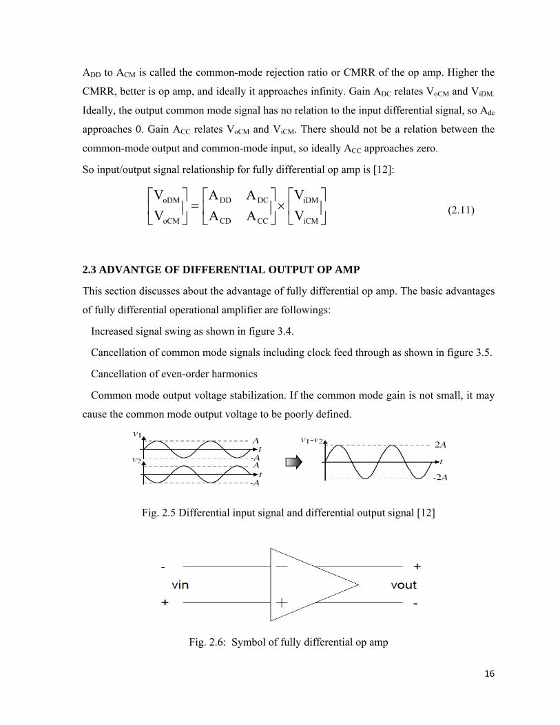
Increased signal swing as shown in figure 3.4.
Cancellation of common mode signals including clock feed through as shown in figure 3.5.
Cancellation of even-order harmonics
Common mode output voltage stabilization. If the common mode gain is not small, it may
cause the common mode output voltage to be poorly defined.
Fig. 2.5 Differential input signal and differential output signal [12]
Fig. 2.6: Symbol of fully differential op amp
17
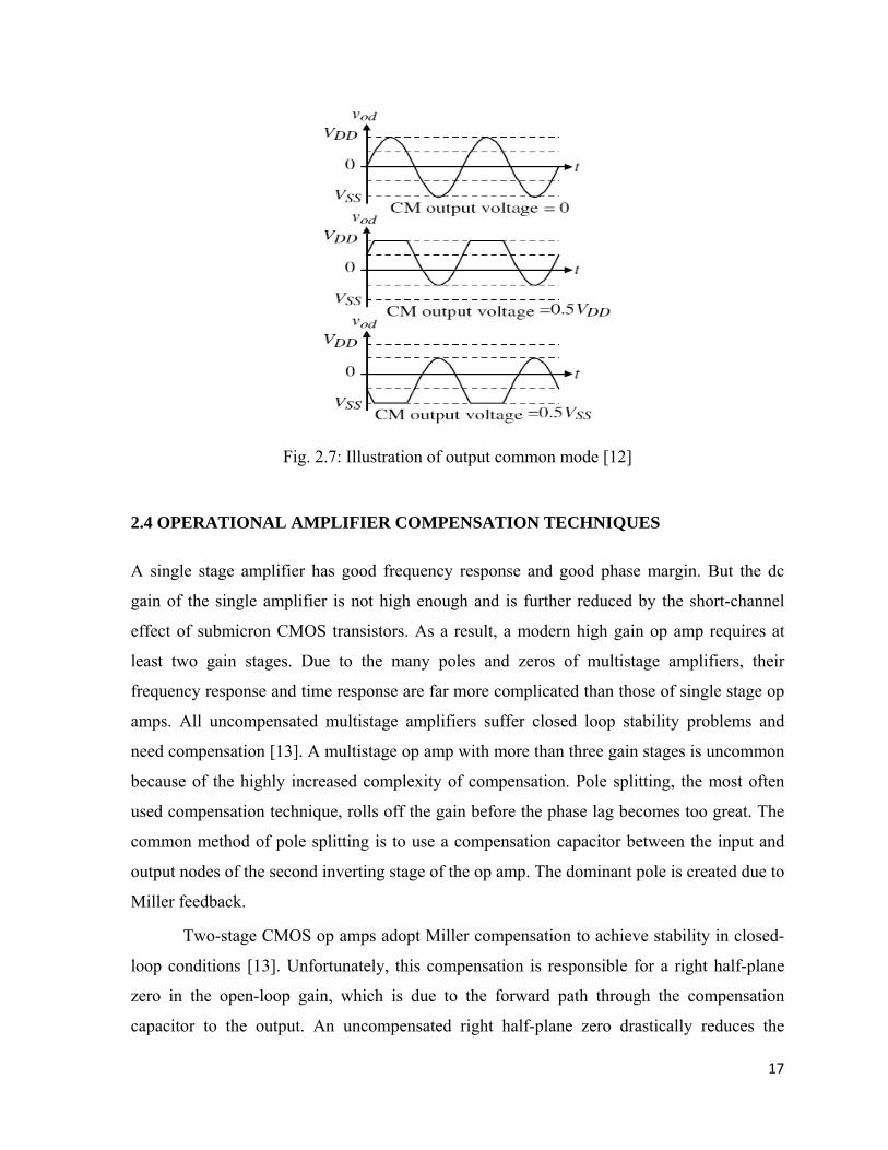
Fig. 2.7: Illustration of output common mode [12]
2.4 OPERATIONAL AMPLIFIER COMPENSATION TECHNIQUES A single stage amplifier has good frequency response and good phase margin. But the dc
gain of the single amplifier is not high enough and is further reduced by the short-channel
effect of submicron CMOS transistors. As a result, a modern high gain op amp requires at
least two gain stages. Due to the many poles and zeros of multistage amplifiers, their
frequency response and time response are far more complicated than those of single stage op
amps. All uncompensated multistage amplifiers suffer closed loop stability problems and
need compensation [13]. A multistage op amp with more than three gain stages is uncommon
because of the highly increased complexity of compensation. Pole splitting, the most often
used compensation technique, rolls off the gain before the phase lag becomes too great. The
common method of pole splitting is to use a compensation capacitor between the input and
output nodes of the second inverting stage of the op amp. The dominant pole is created due to
Miller feedback.
Two-stage CMOS op amps adopt Miller compensation to achieve stability in closed-
loop conditions [13]. Unfortunately, this compensation is responsible for a right half-plane
zero in the open-loop gain, which is due to the forward path through the compensation
capacitor to the output. An uncompensated right half-plane zero drastically reduces the

18
maximum achievable gain-bandwidth product, since it makes a negative phase contribution
to the open-loop gain at a relatively high frequency.
Fig. 2.8: Simple two stage operational amplifier [13]
As a consequence, in the design of two stage op amps, compensation of the right half-plane
zero is required. After the compensation of the right half-plane zero, the maximum
achievable gain-bandwidth product is limited by the second pole.
Fig. 2.9 (a) Nulling-resistor compensation block. (b) Voltage buffer
compensation block. (c) Current buffer compensation block [13]
Indeed, in order to guarantee an adequate phase margin, we must properly set the ratio of the
second pole to the gain-bandwidth product, GBW. GBW depends both on the trans-
conductance of the first stage, gm1, and on the compensation capacitance, CC, and is given by

19
C
1m
C2gGBWπ
= (2.12)
Various techniques for compensation of the right half-plane zero in two-stage CMOS op
amps are nulling-resistor compensation, voltage-buffer compensation and current buffer
compensation [13][14]. Figure 2.9 elaborates schematically the above said methods that are
implemented as per the required design.
Next section discusses literature review of common mode feedback (CMFB) technique used
in most of the designs in work.
2.5 COMMON MODE FEEDBACK
For proper operation of a fully differential amplifier, common mode feedback (CMFB) is
required to fix the voltages at high impedance nodes in the circuit to their desired values [15].
Because a two stage design is employed with two inversions, the CMFB also must be
inverting. This is accomplished by a switched-capacitor circuit and PMOS differential pair
which adjusts the common mode level of the first stage by either injecting current into or
bleeding current from the input legs as needed. The common mode output of the first stage is
set to the point which minimizes the quiescent current in the second stage. The common
mode voltage of the second stage is also dynamically adjusted using common mode feedback
transistors. These transistors help to correct the inherent imbalance in pulling between
NMOS in PMOS in a class AB stage during switching. In order not to degrade the overall
speed of the amplifier, the unity gain bandwidth of the CMFB circuits must be greater than
that of the main amplifier [15].
2.5.1 PRIMARY REASON FOR COMMON MODE FEEDBACK
Since each of input transistors carries a current of ISS/2 where ISS the tail current of the first
stage of op amp ( as shown figure 3.3), the CM level depends on how close drain currents ID3
and ID4 are to this value. In practice, as exemplified by figure 2.10, mismatches in the PMOS
and NMOS current mirrors defining ISS and ID3,4 create a finite error between ID3,4 and ISS.
For high gain amplifiers, one wishes a p-type current source to balance an n-type current
source [2]. As illustrated in figure 2.10, the difference between IP and IN must flow through
intrinsic output impedance of the amplifier, creating an output voltage change of

20
( )( )NPNP RRII ||− . Since the current error depends on mismatches and NP RR || is quite high,
the voltage error may be large, thus driving p-type and n-type current sources into triode
region. As a general rule, the output CM level cannot be determined by visual inspection and
requires calculation based on device properties. Thus we emphasize that differential feedback
cannot define the CM level [2].
Fig. 2.10 Current mismatch problem [2]
The sensing method suffers from an important drawbacks, it limits the differential output
swings. Since the common-mode loop gain is not large enough to keep the common-mode
voltages steady we must add an external circuit to implement a high-gain Common-Mode
Feedback (CMFB) loop [2]. A block diagram of a fully-differential op amp with CMFB is
shown below in figure 2.11. The gain parameters ADD, ACD, ADC, and ACC are the same as
shown in equation (2.11). The new gain parameters ASD, ASD, ADS, and ACS model how the
CMFB circuit will affect the op amps behavior.
The gain parameters ASD and ASC model how the CM control signal Vs affects both
VODM and VOCM. Ideally, the CMFB circuit should keep VCM stable without influencing
VODM. Thus, ASC should be large and ideally approach infinity and ASD should be small and
ideally approach 0. The gain parameters ADS and ACS relate the CM control voltage Vs to
VODM and VOCM, respectively. We want the CM sense circuit to generate a control voltage Vs
which is dependant only on the output CM voltage and reject the differential mode (DM)
output voltage. Thus, we want ADS to be small and ideally approach 0, and ACS to be large
and ideally approach infinity. Given this the following approximations hold: VOCM ≈ ASC*VS

21
and VS ≈ ACS * VOCM. From this we can get one of the most important performance
parameters of the CMFB loop, namely the CMFB loop gain which is equal to
ACML=(ASC*ACS) [16].
Fig. 2.11 Fully differential amplifier with CMFB [16]
To minimize the offset in VoCM, ACML should be designed to be as large as possible, and
ideally it approaches infinity. Since in a real world implementation the magnitude of ASC and
ACS will be a function of frequency, one wants a large magnitude for ACML with a bandwidth
as large as the bandwidth of the differential mode bandwidth of the op amp. A CMFB circuit
averages both differential output voltages to produce a common mode voltage VCM. Voltage
VCM is then compared to a desired reference common-mode voltage, VCM, usually equal to
the average of the two power supplies, or analog ground. The difference between VCM and
VCMS is amplified and this error voltage is used to change the common-mode bias current of
the op amp to force VCM and VCMS to be equal..
The I/O signal relationships for fully differential Op amp with CMFB are given by [17]
⎥⎥⎥
⎦
⎤
⎢⎢⎢
⎣
⎡×⎥
⎦
⎤⎢⎣
⎡=⎥
⎦
⎤⎢⎣
⎡
S
iCM
iDM
SCCCDC
SDCDDD
OCM
ODM
VVV
AAAAAA
VV
(2.13)
[ ] [ ] ⎥
⎦
⎤⎢⎣
⎡×=
OCM
ODMCSDSS V
VAAV (2.14)
The current in the CMFB circuit does not need to be large as long as the currents through the
top and bottom of the OTA are fairly well balanced. Since the common mode feedback
22
circuit only adds to the bias current in the bottom of the circuit, it is expected that the bias
currents in top half will be slightly lower.
Most CMFB circuits can be divided into three general categories: Switched-Capacitor
(SC) CMFB circuits, differential difference amplifier (DDA) CMFB circuits or resistor-
averaged CMFB circuits. The major distinction between these three categories is the
technique used to average the differential output voltages to produce the common mode
voltage VCM.
2.6 SIMULATION METHODS
Simulation methods for gain, bandwidth, phase margin, ICMR, CMRR, PSRR, transient
response etc are shown in this section. These are the general methods collected from
literature [1] [2] for determining various parameters of an operational amplifier.
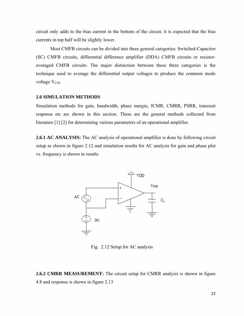
2.6.1 AC ANALYSIS: The AC analysis of operational amplifier is done by following circuit
setup as shown in figure 2.12 and simulation results for AC analysis for gain and phase plot
vs. frequency is shown in results
Fig. 2.12 Setup for AC analysis
2.6.2 CMRR MEASUREMENT: The circuit setup for CMRR analysis is shown in figure
4.8 and response is shown in figure 2.13

23
Fig. 2.13 Setup for CMRR measurement
2.6.3 PSRR MEASUREMENT: For the measurement of PSRR, op amp is connected in
unity gain feedback, a DC bias is connected to input and AC signal at VDD terminal for
PSRR measurement. Setup for PSRR measurement is shown in figure 2.14
Fig. 2.14 Setup for PSRR measurement
2.6.4 ICMR MEASUREMENT: For ICMR measurement apply variable DC voltage at
input of opamp in unity gain configuration as shown in figure 2.15.
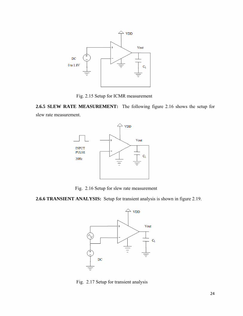
24
Fig. 2.15 Setup for ICMR measurement
2.6.5 SLEW RATE MEASUREMENT: The following figure 2.16 shows the setup for
slew rate measurement.
Fig. 2.16 Setup for slew rate measurement
2.6.6 TRANSIENT ANALYSIS: Setup for transient analysis is shown in figure 2.19.
Fig. 2.17 Setup for transient analysis

25
CHAPTER 3 DESIGN OF SIMPLE TWO STAGE AND TELESCOPIC AMPLIFIER This Chapter deals with the design of the following types of amplifiers:
1. Simple Two Stage Amplifier
2. Two Stage Telescopic Amplifier
3.1 DESIGN OF SIMPLE TWO STAGE AMPLIFIER
This section presents a basic two-stage CMOS op amp design procedure that provides the
circuit designer with a means to strike a balance between two important characteristics in
electronic circuit design, namely high speed performance and high gain for fine accuracy.
CMOS op amps are ubiquitous integral parts in various analog and mixed-signal
circuits and systems. The two-stage CMOS op amp is widely used because of its simple
structure and robustness. In designing an op amp, numerous electrical characteristics, e.g.,
gain-bandwidth, slew rate, common-mode range, output swing, offset, all have to be taken
into consideration. Furthermore, since op amps are designed to be operated with negative-
feedback connection, frequency compensation is necessary for closed-loop stability.
Unfortunately, in order to achieve the required degree of stability, generally indicated by
phase margin, other performance parameters are usually compromised. As a result, designing
an op amp that meets all specifications needs a good compensation strategy and design
methodology [8].
Fig. 3.1: Block Diagram of basic Op amp [1]

26
Classical op amp architecture is made up of three stages as shown in figure 3.1, even though
it is often referred to as a “two-stage” op amp, ignoring the buffer stage. The first stage
usually consists of a high-gain, differential amplifier. This stage has the most dominant pole
of the system. A common source amplifier usually meets the specifications of the second
stage, having a moderate gain. The third stage is most commonly implemented as a unity
gain source follower with a high frequency and negligible pole [2].
A typical CMOS differential amplifier stage is given in figure 3.2. Differential
amplifiers are often desired as the first stage in an op amp due to their differential input to
single ended output conversion and their high gain. The high gain requirement indicates that
either a very high-gain single stage or two modest gain stages are needed. The main
disadvantage of the single stage implementation is the low output range [12]. One of the
biggest benefits of the two-stage approach is that the net open loop gain can be achieved with
two distinct stages,
Fig. 3.2 A classic Two Stage Op amp Architecture
thereby eliminating much of the complexity involved in designing a single gain stage and
leaving the distribution of gain in each stage up to the designer’s discretion. The first-stage
does not have to drive the large capacitive load at the output of the second stage. The most

27
logical approach would be to have a large gain in the first stage and a small gain and high
swing in the second, the reason being that low second stage gain would not greatly amplify
first stage noise and high swing would give better dynamic range [18].
There are several benefits of a two-stage topology compared to that of a single stage
amplifier. First and foremost is that the net amplifier gain required can be realized in two
stages, thus de-coupling gain and headroom considerations. Typically, the majority of the
gain is realized in the first stage. Secondly, the second stage or output stage can be designed
Fig. 3.3 Schematic of Fully Differential Two Stages OTA
to simultaneously source large currents and have a large output swing since its gain
requirements are significantly reduced by the two-stage topology. Also, the noise in a two-
stage amplifier is comparable to that of a single stage amplifier. This is because very little
input referred noise is contributed by the second stage due to the typically large gain in the
first stage. Consequently, the total output noise is primarily due to only the first stage of the
amplifier.
The major drawback of a two-stage design is that of speed. This is due to the additional non-
dominant pole added by cascading the two stages. However, a compensation capacitor can be
used to offset this issue. Thus the two-stage design with compensation capacitor was chosen
28
over the single stage. However, the two-stage design is more flexible than that of a single
stage design. This suggests that the slowness of the two-stage design can be compensated for
without having to trade off significantly in terms of gain, and dynamic range. Upon
comparison of the single stage to two-stage topologies, it is found that the advantages of the
two stage topology have outweighed its disadvantages. Consequently, a two-stage design
over single stage design is opted.
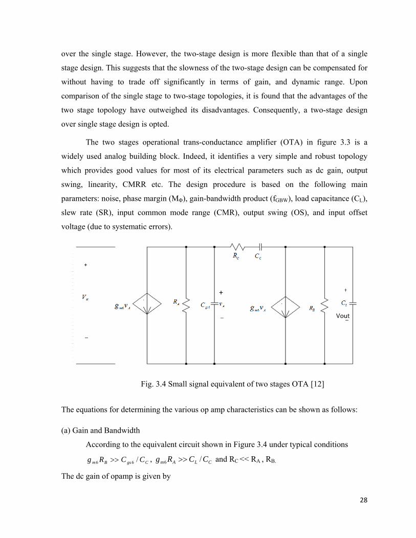
The two stages operational trans-conductance amplifier (OTA) in figure 3.3 is a
widely used analog building block. Indeed, it identifies a very simple and robust topology
which provides good values for most of its electrical parameters such as dc gain, output
swing, linearity, CMRR etc. The design procedure is based on the following main
parameters: noise, phase margin (MΦ), gain-bandwidth product (fGBW), load capacitance (CL),
slew rate (SR), input common mode range (CMR), output swing (OS), and input offset
voltage (due to systematic errors).
Fig. 3.4 Small signal equivalent of two stages OTA [12]
The equations for determining the various op amp characteristics can be shown as follows:
(a) Gain and Bandwidth
According to the equivalent circuit shown in Figure 3.4 under typical conditions
CgsBm CCRg /66 >> , CLAm CCRg /6 >> and RC << RA , RB.
The dc gain of opamp is given by

29
Av0=gm1gm6RARB (3.1)
The op amp’s dominant pole frequency and unity-gain bandwidth, also commonly known as
gain-bandwidth, can be found to be
CBAmP CRRg 6
11
=ω and C
mU C
g 1=ω = 110 PmV gA ω= (3.2)
Where ωP1 and ωU are dominant pole and unity gain bandwidth respectively. The transfer
function of two stage OTA is given by [7]:
( ) 3CL6gCBA
2CLC6gL6gBACBA6m
C6m
C
0VID
OUT
sCCCRRRsCCCCCCRRsCRRg1
Rg
1sC1A
VV
+++++
⎟⎟⎠
⎞⎜⎜⎝
⎛−−
=
(3.3)
(b) Output Swing
By defining OUTHRV as the voltage head room voltage at output, i.e
+OUT
HRV = VDD –Vout(max) and −OUT
HRV = Vout(min) –VSS
(c) Common Mode range
If we define VCM as the opamp input common mode range i.e
VCM+= VDD- VCM(max) and VCM
- = VCM(min) – VSS
According to Figure 2.8, it can be shown that
VCM+ = Veff3 – Vtn and VCM
- = Veff5+ Veff1,2 + Vtn
(d) Internal Slew Rate
The slew rate associated with CC is found to be
C
5D
CI
SR = (3.4)
The slew rate associated with CL is found to be
L
5D7D
CII
SR−
= (3.5)
Combining both (2.15) and (2.16) we obtain
)CC(SRI LC7D += (3.6)

30
The Simple two stage op amp can be designed using PMOS as input transistors also. It has
some advantages and disadvantages as compared to NMOS as input transistors. The
advantages include less flicker noise, wide lower output swing and better phase margin. The
disadvantages include lower gain as compared to NMOS for the same sizes. This is due to
lower transconductance of PMOS as compared to NMOS and hence the lower bandwidth
[19].
3.2 DESIGN PROCEDURE OF SIMPLE TWO STAGE OP AMP
For Simple Two Stages Op Amp design (fig 3.2) classical design approach has been followed
[13]. Starting from the design specification, the sizes of all transistors has been calculated.
After using theses sizes the specifications were not completely matched. This is due to deep
sub-micron technology (180nm used in this work) behavior. Generally Sizes are calculated
using the classical square law equations which are not suitable for lower micron technology.
So, some tweaks in the designs has been done in order to achieve the required specification.
The main design steps of simple two stage op amp are as follows:
1. Choose I7 to be as a value which will be decided by slew rate and power dissipation.
2. Find the value of compensation capacitor Cc= I7/Slew Rate(SR) also we can use
approximation that Cc > 0.22 CL [1]
3. Find gm1 from gain bandwidth=gm1/2π*Cc
4. Find gm5 from condition of stability gm6~2.2*gm1
5. Gain Av = ) g + (g ) g + (g
gg
ds5ds6ds4ds2
m6 m1 ×
= I ) + ( )I + (
gg
5DS5 6DS242
m6 m1
λλλλ×
6. Calculate I5 > (CC + CL ) SR
7. Find out I5 from steps 5 and 6
31
8. Find (W/L)1,2 from (gm = )I L(W/ K 2 DS )
9. Then (W/ L)6 from ( W/L = DS
2m
KI2g )
10. M3, M4 are matched devices. For matching of the mirror voltages VDS3 = VDS4. And
since VGS3 = V DS3 and VDS4 = VGS6 then VGS3 = VGS6. So , one can calculate
(W/ L)3= (W/ L) 6* ⎟⎟⎠
⎞⎜⎜⎝
⎛
5DS
3DS
II
(3.7)
11. The W/L ratio of current sinks M7 and M5 can be found from common current equation
of the mosfet.
12. The value of nulling resistor Rz can be calculate by
Rz = 6
1
mg ⎟⎟
⎠
⎞⎜⎜⎝
⎛ +
C
CL
CCC
(3.8)
Both, single ended and fully differential Simple Two Stages Amplifiers with NMOS as input
transistors has been designed. The above described design procedure is for single ended two
stage op amp. For fully differential amplifier design, a bias voltage is connected to the gate of
both PMOS load transistors of first stage instead of gate–drain connection. This will slightly
change the output node voltages. One can easily tweak the design to meet the specifications.
3.3 SIMULATION RESULTS.
Simple two stage op amp was designed using above mentioned procedure and the simulation
results obtained are shown in this section.
The single ended simple two stage op amp used in this section provides all necessary
parameters required to use it as unity gain buffer in the single ended architecture of 8-bit,
40MSPS pipelined ADC. Similarly, the fully differential simple two stage op amp designed
in this section fulfills all the requirements for unity gain buffer of the fully differential
architecture of the pipelined ADC. The results obtained for both op amps are as follows:
32
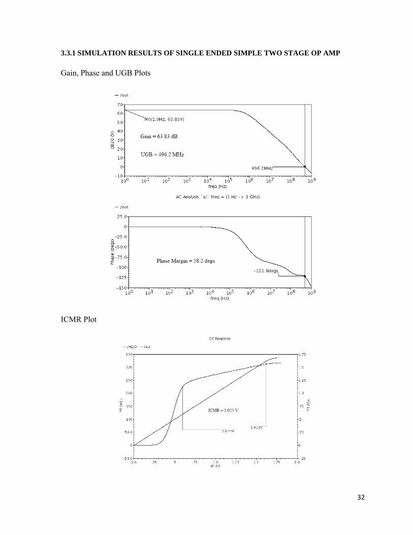
3.3.1 SIMULATION RESULTS OF SINGLE ENDED SIMPLE TWO STAGE OP AMP
Gain, Phase and UGB Plots
ICMR Plot
33
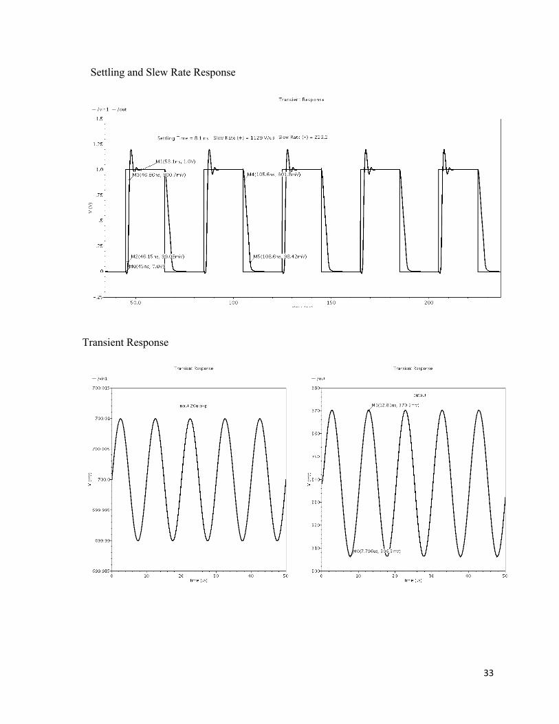
Settling and Slew Rate Response
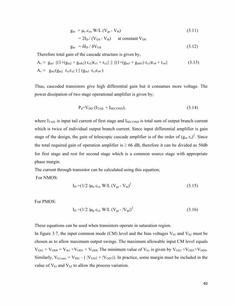
Transient Response

34
CMRR and PSRR Plots
3.3.2 SIMULATON RESULTS OF FULLY DIFFERENTIAL SIMPLE TWO STAGE OP
AMP
ICMR Plot
35
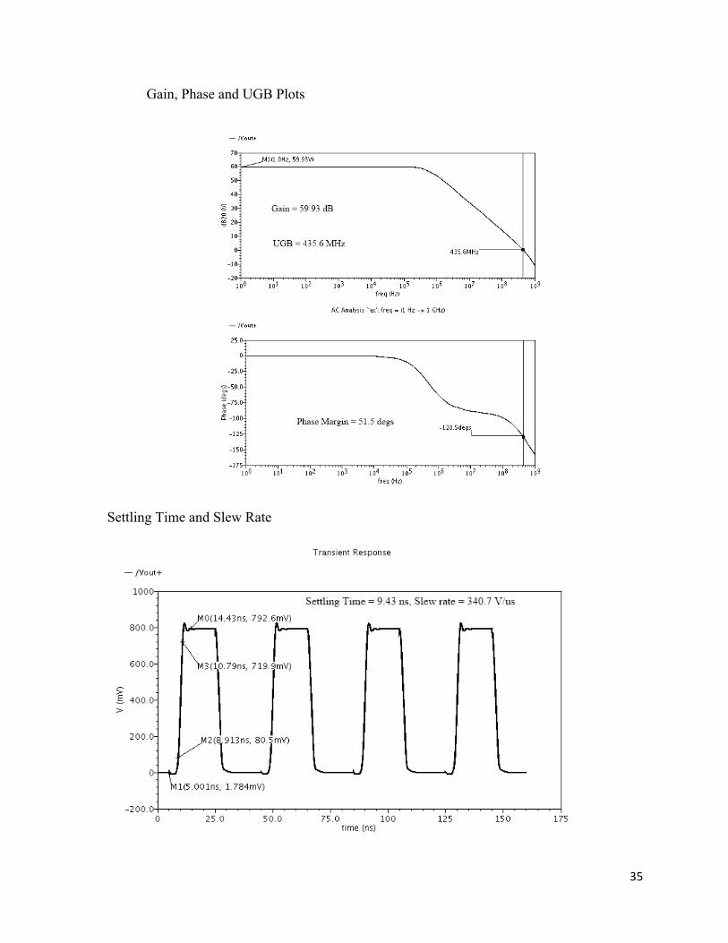
Gain, Phase and UGB Plots
Settling Time and Slew Rate
36
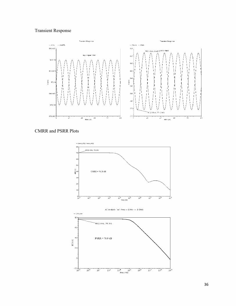
Transient Response
CMRR and PSRR Plots

37
3.4 TELESCOPIC OP AMP DESIGN
Cascode configurations may be used to increase the voltage gain of CMOS transistor
amplifier stages. This structure has been called a ‘telescopic-cascode’ op amp because the
cascodes are connected between the power supplies in series with the transistors in the
differential pair, resulting in a structure in which the transistors in each branch are connected
along a straight line. The main potential advantage of telescopic cascode op amps is that they
can be designed so that the signal variations are entirely handled by the fastest-polarity
transistors in a given process [19]. In the first stage, one was simply looking for a
configuration that allowed for high gain, low noise and minimal current since output swing is
less critical. The folded cascode and the telescopic configurations were considered since we
required at least one cascoded stage for a gain on the order of (gmro)2. A high swing
configuration still needs to be used to insure that all the devices in this stage are in saturation.
In comparing the two topologies, the folded cascode has more current legs and more devices
in the signal path. This leads to larger static current and more noise contributor [20].
The single stage architecture naturally suggests low power consumption. A telescopic
cascode op amp, as shown in figure 3.5, typically has higher frequency capability and
consumes less power than other topologies. Its high-frequency response stems from the fact
that its second pole corresponding to the source of the n-channel cascode devices is
determined by the trans-conductance of n-channel devices as opposed to p- channel devices,
as in the case of a folded cascode. Also the parasitic capacitance at this node arises from only
two transistors instead of three, as in the latter. The single stage architecture naturally
suggests low power consumption.
The disadvantage of a telescopic op amp is severely limited output swing. It is
smaller than that of the folded cascode because the tail transistor directly cuts into the output
swing from both sides of the output. In the telescopic op amp shown in figure 3.5, all
transistors are biased in the saturation region. Transistors M1–M2, M7-M8, and the tail
current source M9 must have at least VDsat to offer good common mode rejection, frequency
response, and gain [22]. The maximum output voltage depends on the common-mode input.
However, this limitation as well as the limitation on the common-mode input range can be
overcome in switched-capacitor circuits. Such circuits allow the op amp common-mode input

38
voltage to be set to a level that is independent of all other common-mode voltages on the
same integrated circuit.
(a) (b)
Fig. 3.5: (a) Single ended and (b) Fully Differential Single Stage Telescopic op-amp [2]
The target was to design single stage fully differential amplifier with high DC gain
and high unity gain bandwidth. The first and probably the most important step of the design
is to select an amplifier topology that have the ability to meet all requirements and
specifications of the design. Besides that, the topology which consumes low power
dissipation is also taking into consideration. The topologies that will certainly satisfy
magnitude of DC gain is either telescopic cascode op amp or folded cascode op amp. The
telescopic cascode op amp typically has higher frequency capability and consumes less
power than other topology. Besides that, it has fewer current legs, consumes less power and
adds less noise to the signal path. The telescopic amplifier has only four transistors in the
signal path contributing significant noise power, whereas the folded cascode has six
39
transistors. The single stage architecture naturally suggests low power consumption.
Therefore, telescopic amplifier has been selected as shown in figure 3.5.
3.5 DESIGN OF FIRST STAGE TELESCOPIC AMPLIFIER
In this section the design concepts of the telescopic differential amplifier shown in figure 3.5
has been discussed. All transistors must be in saturation region of operation. This is because
to ensure the performance obtained will be constant over a wide range of voltage. Since
schematic is of balance in nature, so we take half circuit method to find its dc gain.
Fig. 3.6: Half circuit of telescopic cascode
Now, consider the small signal characteristics of a cascode stage, assuming all transistors
operates in saturation. MOS device when operates in saturation region, their current is almost
constant. The voltage gain is equal to that of common source stage because the drain current
produced by input device must flow through the cascode device. An essential property of the
cascode structure is its high output impedance. The output impedance (Rout ) of the schematic
as shown in figure 3.6 is calculated as;
Rout = (1+(gm2 + gmb2) ro2)ro1 + ro2 || (1+(gm3 + gmb3) ro3)ro4 + ro4 (3.9)
The gain can be calculated as
Av ≈ -Gm Rout where Gm ≈ gm1 (3.10)
The value of gm1 is the trans-conductance of input transistor M1. The trans-conductance gm of
MOS transistor can be calculated as:
40
gm = μn cox W/L (Vgs - Vth) (3.11)
= 2ID / (VGS - Vth) at constant VDS
gm = δID / δVGS (3.12)
Therefore total gain of the cascade structure is given by,
Av ≈ gm1 (1+(gm2 + gmb2) ro2)ro1 + ro2 || (1+(gm3 + gmb3) ro3)ro4 + ro4 (3.13)
Av ≈ gm1(gm2 ro1ro2 ) || (gm3 ro3ro4 )
Thus, cascoded transistors give high differential gain but it consumes more voltage. The
power dissipation of two stage operational amplifier is given by;
Pd=VDD (ITAIL + ISECOND), (3.14)
where ITAIL is input tail current of first stage and ISECOND is total sum of output branch current
which is twice of individual output branch current. Since input differential amplifier is gain
stage of the design, the gain of telescopic cascade amplifier is of the order of (gm ro)2. Since
the total required gain of operation amplifier is ≥ 66 dB, therefore it can be divided as 50db
for first stage and rest for second stage which is a common source stage with appropriate
phase margin.
The current through transistor can be calculated using this equation;
For NMOS:
ID =(1/2 )μn cox W/L (Vgs - Vtn)2 (3.15)
For PMOS:
ID =(1/2 )μp cox W/L (Vgs - |Vtp|)2 (3.16)
These equations can be used when transistors operate in saturation region.
In figure 3.7, the input common mode (CM) level and the bias voltages Vb1 and Vb2 must be
chosen as to allow maximum output swings. The maximum allowable input CM level equals
VGS1 + VOD9 = Vth1 +VOD1 + VOD9. The minimum value of Vb1 is given by VGS3 +VOD1+VOD9.
Similarly, Vb2,max = VDD – ( |VGS5| + |VOD7|). In practice, some margin must be included in the
value of Vb1 and Vb2 to allow the process variation.

41
The design of telescopic cascade op amp starts with the sizing of the main input differential
pair which are transistor M1 and M2. Care has to be taken not to make the input pair too big
to affect the bandwidth and at the same time making them big enough to provide enough gm
and therefore providing higher gain. The NMOS M1 and M2 cascode transistors are then
sized to act as buffer between input pair and the output. The PMOS cascode load transistors
are designed to steer the required amount of current through both the legs. So, the PMOS
cascode transistors are sized such that it will not load the output with huge parasitic
capacitance. The Current ID = Iss / 2, so we can write,
ro1 ≈ 1/λn Id ≈ ro2 (3.17)
ro3 ≈ 1/λp Id ≈ ro4 (3.18)
For biasing all the transistors in saturation region, the condition of saturation of each type of
MOSFET must be satisfied. Set the Vincm= 0.9V and Vtail = 0.51V for current source tail
transistor and assume that the output DC level at 0.9V for better response. Also by
calculations, Vb1 ≈ 1.2V, Vb3 ≈ 1.2V. By applying all condition these bias voltage condition
are obtained as shown in half circuit figure 3.7.
After employing all equations and using some iterations, the single stage of telescopic
differential amplifier has been designed. Next section explains the design how to design two
stage fully differential telescopic op amp. This is nothing but an extension of the design
procedure followed for single stage.
3.6 DESIGN OF TWO STAGES FULLY DIFFERENTIAL TELESCOPIC OP AMP The conversion rate and the resolution of the pipeline ADC are fully determined by the op
amp performance. As a result, the op amp employed in the high-speed high-resolution ADC
should provide high dynamic range under low power supply and make a compromise among
all limitations, such as settling time, input common mode range, output swing, power supply
rejection ratio, power consumption and so on. The op amp performance requirement of the
first pipeline stage must be the most rigorous to maintain better linearity. The op amps of the
rest stages could be scaling down to minimize the power consumption. As shown in Figure
3.7, a two-stage cascode compensation op amp is designed, which has many merits, such as

42
high gain, large bandwidth and large output swing. The op amp in the first stage employs
fully-differential telescopic cascode OTA.
Fig. 3.7: Fully Differential two stage telescopic amplifier
Since NMOS electron mobility μn is larger than PMOS electron mobility μp by 3~4 times, the
input differential pairs use NMOS transistors. This structure can provide higher gain and be
more suitable for low power consumption than folded cascode structure. The second stage is
fully differential common-source amplifiers which use current-source transistors as loads to
provide higher gain and larger output swing. However, inner high impedance nodes of two-
stage op amp introduce low frequency poles which cause the closed loop characteristic
instability. Thus, frequency compensation technology needs to be introduced to maintain
stability of the two-stage op amp. Comparing with Miller compensation, cascode
compensation capacitor could achieve larger bandwidth.

43
Now consider the fully differential telescopic cascode, in addition various useful properties
of differential operation, this topology avoids the mirror pole, thereby exhibiting stable
behavior for a greater bandwidth. In fact, one can identify one dominant pole at each output
node and one non-dominant pole arising from output node. This suggests the fully
differential telescopic cascode circuits are quite stable. The capacitance at node N in figure
3.6 is
CN = CGS5 + CSB5 + CGD7 + CDB7 (3.19)
The CN shunts the output resistance of M7 at high frequencies, thereby dropping the output
impedance of the cascode. The Zout of the single stage fully differential op amp is;
Zout = 1+ gm5 ro5) ZN + ro5 where body effect is neglected and ZN = ro7 || (CNs)-1 (3.20)
We have,
Zout = (1+ gm5 ro5) ro7 || (CNs)-1 (3.21)
Now, we take the output load capacitance into account;
Zout || (1/CLs) = )(1/C + ))(C || r )(r g +(1 )(1/C* ))(C || r )(r g +(1
Ls1-
Nso7o5m5
Ls-1
Nso7o5m5
(3.22)
= 1 + )]C r + Cr )r g +[(1
r )r g +(1
No7Lo7o5m5
o7o5m5 (3.23)
Thus, the parallel combination of Zout and load capacitance (CL) still contains a single pole
corresponding to a time constant [(1+ gm5 ro5) ro7CL + ro7 CN)].
3.7 DESIGN PROCEDURE FOR TELESCOPIC OP AMP
The design procedure of telescopic amplifier is being presented here. A general design
procedure is presented in this section, which requires slight modification from single ended
to fully differential telescopic op amp design. The two important points which have been
followed in this and all the designs in this thesis report are:
• Using the current and gain-bandwidth specification one can find the gm and the
required W/Ls of input transistors.
• For the rest of the transistors one can find the W/L using Vdsat equation.

44
STEP1: In the first step of the design the estimation of the bias current is done, assuming the
GBW established by the dominant node,
2п fT = Lthgs
SS
C1
)VV(I2− (3.24)
Where ISS is the tail current and fT is the unity gain frequency and CL is the load capacitor. STEP 2: Design Tail transistor M9 and calculate W and L of this transistor by using the
transistor in saturation .The equation used is
ISS = ( )2thgsoxn
VVLW
2C
−μ
(3.25)
STEP 3: Calculate the bias Vcm of transistor M9 using the equation
Vcm = Vgs9 – Vth (3.26)
STEP 4: Both the input transistors have half of ISS current each. Design the differential pair
of the circuit, by assuming both of them to be working in saturation mode. Their aspect ratios
can be calculated using bias current Iss. The equation used is
ISS = oxnCμ ( )2thgs VVLW
− (3.27)
STEP 5: Calculate the common mode voltage that allows M9 to be in saturation
Vin, cm >= Vsat, 9 + Vgs1 (3.28)
STEP 6: The size of PMOS load transistors M5-M8 are calculated by saturation equation.
For M7-M8, a proper bias Vb3 is chosen such that the each transistor remains in saturation.
As same current ISS /2 is flowing in each PMOS load transistor, so sizes can be calculated by
applying the saturation equation for PMOS transistor as,
ISS = oxpCμ ( )2tpsg |V|V
LW
− (3.29)

45
Where Vsg =VDD – Vb3, and Vtp = threshold voltage of PMOS
Similarly sizes of M5-M6 can be calculated using equation (3.29) but now the gate voltage
will be lower than Vb3 as there is overdrive from upper side.
STEP 7: The sizes of transistors of second stage can be calculated in the same way as
explained in section 3.2. Compensation capacitor and nulling resistor values can be
calculated as explained in equation (3.8). Size of transistor M1A and M1B is kept large in
such extent that they remain in deep triode region, still not loading the output of the first
stage and hence not degrading the UGB and slew rate of the whole circuit.
By following the above steps both, single ended two stage and fully differential two stage
telescopic op amp has been designed successfully. The fully differential architecture requires
more design expertise as compared to single ended.
The stability of output node voltages in fully differential mode is the main concern.
The output node voltages should not vary with the variation in input voltage change in the
whole input common mode range. To keep the output node voltage at constant level, a
continuous time common mode feedback technique has been employed as shown in figure
3.7 and has been designed as explained in step 7 above.
3.8 SIMULATION RESULTS OF TELESCOPIC AMPLIFIER
The results obtained from single ended telescopic and fully differential telescopic op amps
have been discussed in this section. The simulation results include important parameters like
Gain, Phase, UGB, settling time, slew rate, CMRR and PSRR etc.
Results obtained for the single ended telescopic op amp are good enough to use it in
the single ended architecture of the 8-bit, 40MSPS pipelined ADC which was targeted as an
application for this work. Fully differential telescopic amplifier designed in this section also
fulfills all the requirements which are needed for fully differential mode of the pipelined
ADC.
One thing that is worth mentioning about the results obtained for the telescopic op
amps. The input common mode range requirement is not much large. This is clear from the
architecture of pipelined ADC stage. Either there is sample phase or hold phase, in both
phases the inputs of op amp remains at common mode level. So, there is no need to worry
about the less ICMR range of the designed telescopic op amps.

46
3.8.1 SIMALTION RESULTS OF SINGLE ENDED TELESCOPIC AMPLIFIER
Gain, Phase and UGB Plots
ICMR :

47
Settling Time and Slew Rate
Transient Response

48
CMRR Plot
PSRR Plot
3.8.2 SIMULATION RESULTS OF FULLY DIFFERENTIAL TELESCOPIC OP AMP
ICMR Plot

49
Gain, Phase and UGB Plots
Settling Time and Slew Rate
50
Transient Response
CMRR and PSRR Plots

51
CHAPTER 4 DESIGN OF FULLY DIFFERENTIAL
FOLDED CASCODE AMPLIFIER 4.1 BASIC FOLDING CONCEPT
In order to alleviate the drawbacks of telescopic cascade op amps, namely limited output
swings and difficulty in shorting the input and output, a “folded cascade” op amp can be used
[2]. The folding idea is depicted in figure below
Fig. 4.1 Basic Folding Concept [2]
52
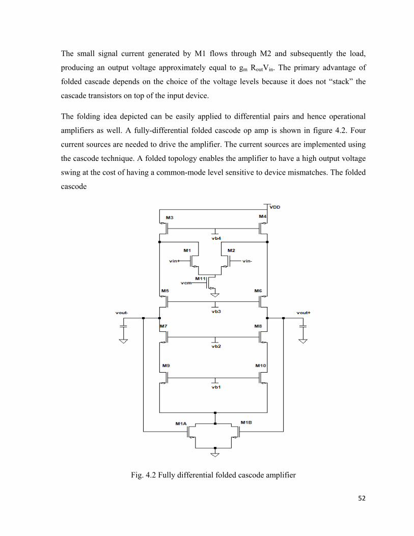
The small signal current generated by M1 flows through M2 and subsequently the load,
producing an output voltage approximately equal to gm RoutVin. The primary advantage of
folded cascade depends on the choice of the voltage levels because it does not “stack” the
cascade transistors on top of the input device.
The folding idea depicted can be easily applied to differential pairs and hence operational
amplifiers as well. A fully-differential folded cascode op amp is shown in figure 4.2. Four
current sources are needed to drive the amplifier. The current sources are implemented using
the cascode technique. A folded topology enables the amplifier to have a high output voltage
swing at the cost of having a common-mode level sensitive to device mismatches. The folded
cascode
Fig. 4.2 Fully differential folded cascode amplifier
53
op amp has a push pull output stage which can sink or source current from the load. The
exact match of the currents in the differential amplifier is not demanded by the folded
cascode op amp since extra current can flow in or out of the current mirrors. While the bias
current of the conventional cascode delivers the current to both the input devices and the
cascode devices since they are stacked together, the bias current ISS of the folded cascade
supplies only the input devices. Additional bias currents are required to add necessary bias
current. In general, the folded cascode connection dissipates more power. The gain of a
folded cascode op amp is normally lower than that of a corresponding conventional cascode
op amp due to the lower impedance of the devices in parallel. A folded cascode op amp has a
pole at the folding connection which is lower compared to that node pole of the conventional
cascode op amp. This is due to the larger parasitic capacitance of extra and possibly wider
devices in the folded structure. Sometimes this low folding pole can self-compensate a folded
cascode if the phase margin is good enough [2].
By applying approximations, the voltage gain of the Operational-Amplifier is given by:
AV=GmRo (4.1)
Where Ro = (gm7 ro7 ( ro1 || ro9)) || (gm5 ro5 ro3 )
There are two dominant poles and a zero which are considered in the study of the frequency
response:
1. First dominant pole, given by the high output resistance (RO) occurs at output node [20]:
ωp1=-1/RoCo (4.2)
Co=CL + CD5 + CD7 (4.3)
2. The second pole which have frequency much greater than dominant pole frequency and is
given by:
ωp2=-1/RCASC CCASC (4.4)
CCASC=CD1+ CS7 + CD9 (4.5)
RCASC ≈ (1/gm7) ||r01||r07 || r09 (4.6)
54
3. Due to the existing a second signal path through Cgd1, a right half plane zero is introduced
in transfer function is calculated as
ωz1 = gm1/Cgd1 (4.7)
There is pole at folding point i.e. the source of M7 & M8 is quite closer to the origin
that associated with the sources of cascode devices. The maximum output voltage swing of
the folded cascode with proper choice of bias voltages, the lower end of the swing is given by
VOD3 + VOD5 and the upper end by VDD – ( |VOD7| + |VOD9| ). Thus, the peak-to-peak swing
on each side is equal to VDD – (VOD3 + VOD5 + |VOD7| + |VOD9| ).
Thus, voltage swing of folded cascade amplifier is slightly higher than that of
telescopic configuration. This advantage comes at the cost of higher power dissipation, lower
voltage gain, lower pole frequencies and higher noise [24][25].
At lower micron level the total gain obtained is comparatively less but unity gain
bandwidth increases appreciably. The gain obtained by single stage is limited to slightly
above 60dB. So, the second stage for folded cascade was also designed to enhance the gain at
the cost of phase margin.
The second stage added to increase the gain adds extra pole and hence decreases the
stability of the design. To overcome this problem, a compensation technique needs to be
applied between input stage and output stage. There are different kinds of compensation
techniques available but simplest RC compensation technique has been employed in this
design. The nulling resistor and capacitor decrease the unity gain bandwidth but that has to
be adjusted by increasing the current in the input stage. Thus choosing suitable values of Rz
and Cc, we can adjust appropriate phase margins for the op amp.
4.2 DESIGN PROCEDURE FOR FOLDED CASCODE OP AMP
Basic design procedure has been followed while designing the folded cascode op amp.
Starting of the design procedure is from basic specification of gain, UGB and settling time.
Followings are the basic steps of designing the folded cascode op amp.
STEP 1: Based on the bandwidth limitation ω the trans-conductance of M1 is chosen, as
input transistors M1 and M2 decide the bandwidth of the op amp.

55
gm1 = 2п * ω*CL (4.8)
STEP 2: Tail current through transistor M11 can be calculated with the following
ISS = SR* CL (4.9)
Where SR = Slew rate of the op amp.
This current will decide how much current can be decided for the output stage. This is
estimated from the power dissipation specification.
P = ITotal * VDD (4.10)
Where ITotal = ISS + Iout. Thus current ISS is decided.
STEP 3: As transistor M1 and M2 are matched, each one would have ISS /2 current flowing
through it. From there the size of M1 and M2 can be calculated.
(W/L)1,2 = 2)(V K
/2)(I 2ovn
SS
(4.11)
Where Kn= µnCox and Vov = Vdsat= Vgs-Vt of the transistor. Value of Vov is decided based on
ICMR requirement. The sizes of M1 and M2 can also be calculated from the following
equation
(W/L)1,2 = 2/I 2K
)(g
SSn
2m1
(4.12)
STEP 4: As explained in step 2, the current in the output stage (Iout) can be decided. Total
current ITotal/2 flows through PMOS transistors M3 and M4. So, again one can calculate their
sizes by deciding the overdrive voltage of each cascode stage.
Current through M5-M10 is Iout/2. So again the sizes of each transistor can be calculated in
the same way.
STEP 5: Up to step 4 only single stage of folded cascode op amp has been designed. To
increase the gain and the swing one can use second stage without using any gain boosting
technique. The current through second stage is generally chosen higher than the first stage.
From that current value and, overdrive of transistors, sizes of transistors of the output stage
can be calculated.
To remove the second pole problem RC compensation technique can be used.
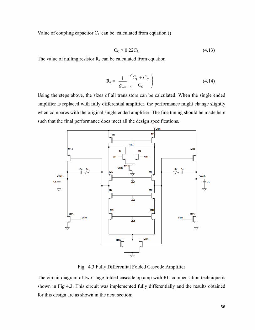
56
Value of coupling capacitor CC can be calculated from equation ()
CC > 0.22CL (4.13)
The value of nulling resistor Rz can be calculated from equation
Rz = 13
1
mg ⎟⎟
⎠
⎞⎜⎜⎝
⎛ +
C
CL
CCC
(4.14)
Using the steps above, the sizes of all transistors can be calculated. When the single ended
amplifier is replaced with fully differential amplifier, the performance might change slightly
when compares with the original single ended amplifier. The fine tuning should be made here
such that the final performance does meet all the design specifications.
Fig. 4.3 Fully Differential Folded Cascode Amplifier
The circuit diagram of two stage folded cascade op amp with RC compensation technique is
shown in Fig 4.3. This circuit was implemented fully differentially and the results obtained
for this design are as shown in the next section:

57
4.3 SIMULATION RESULTS FOR FOLDED CASCODE
Gain, Phase and UGB Plots
ICMR Plot

58
Settling Time and Slew Rate
Transient Response
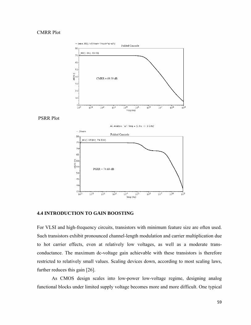
59
CMRR Plot
PSRR Plot
4.4 INTRODUCTION TO GAIN BOOSTING
For VLSI and high-frequency circuits, transistors with minimum feature size are often used.
Such transistors exhibit pronounced channel-length modulation and carrier multiplication due
to hot carrier effects, even at relatively low voltages, as well as a moderate trans-
conductance. The maximum dc-voltage gain achievable with these transistors is therefore
restricted to relatively small values. Scaling devices down, according to most scaling laws,
further reduces this gain [26].
As CMOS design scales into low-power low-voltage regime, designing analog
functional blocks under limited supply voltage becomes more and more difficult. One typical
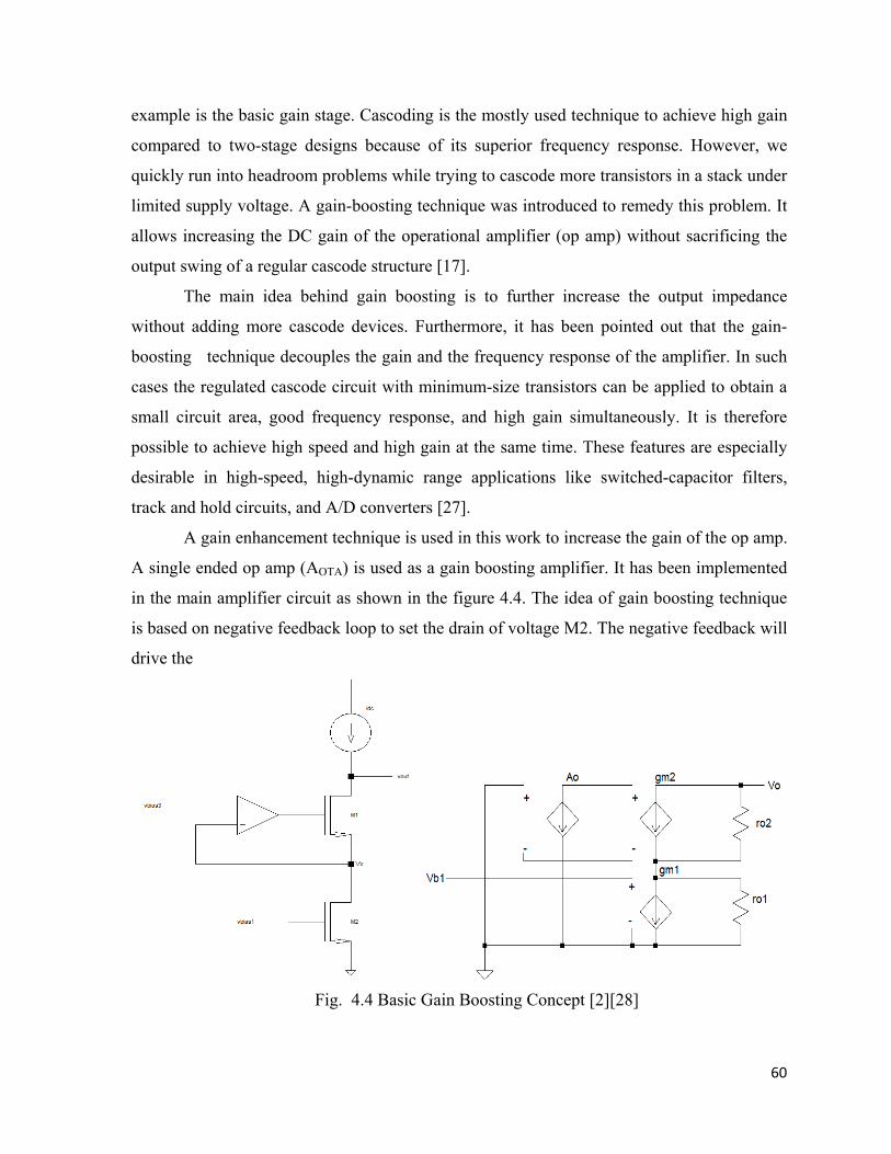
60
example is the basic gain stage. Cascoding is the mostly used technique to achieve high gain
compared to two-stage designs because of its superior frequency response. However, we
quickly run into headroom problems while trying to cascode more transistors in a stack under
limited supply voltage. A gain-boosting technique was introduced to remedy this problem. It
allows increasing the DC gain of the operational amplifier (op amp) without sacrificing the
output swing of a regular cascode structure [17].
The main idea behind gain boosting is to further increase the output impedance
without adding more cascode devices. Furthermore, it has been pointed out that the gain-
boosting technique decouples the gain and the frequency response of the amplifier. In such
cases the regulated cascode circuit with minimum-size transistors can be applied to obtain a
small circuit area, good frequency response, and high gain simultaneously. It is therefore
possible to achieve high speed and high gain at the same time. These features are especially
desirable in high-speed, high-dynamic range applications like switched-capacitor filters,
track and hold circuits, and A/D converters [27].
A gain enhancement technique is used in this work to increase the gain of the op amp.
A single ended op amp (AOTA) is used as a gain boosting amplifier. It has been implemented
in the main amplifier circuit as shown in the figure 4.4. The idea of gain boosting technique
is based on negative feedback loop to set the drain of voltage M2. The negative feedback will
drive the
Fig. 4.4 Basic Gain Boosting Concept [2][28]
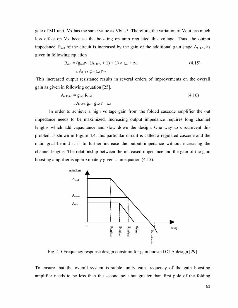
61
gate of M1 until Vx has the same value as Vbias3. Therefore, the variation of Vout has much
less effect on Vx because the boosting op amp regulated this voltage. Thus, the output
impedance, Rout of the circuit is increased by the gain of the additional gain stage AOTA, as
given in following equation
Rout = (gm1ro1 (AOTA + 1) + 1) × ro2 + ro1 (4.15)
≈ AOTA gm1ro1 ro2
This increased output resistance results in several orders of improvements on the overall
gain as given in following equation [25].
AvTotal = gm2 Rout (4.16)
≈ AOTA gm1 gm2 ro1 ro2
In order to achieve a high voltage gain from the folded cascode amplifier the out
impedance needs to be maximized. Increasing output impedance requires long channel
lengths which add capacitance and slow down the design. One way to circumvent this
problem is shown in Figure 4.4, this particular circuit is called a regulated cascode and the
main goal behind it is to further increase the output impedance without increasing the
channel lengths. The relationship between the increased impedance and the gain of the gain
boosting amplifier is approximately given as in equation (4.15).
Fig. 4.5 Frequency response design constrain for gain boosted OTA design [29]
To ensure that the overall system is stable, unity gain frequency of the gain boosting
amplifier needs to be less than the second pole but greater than first pole of the folding

62
cascode amplifier. Figure 4.5 shows the benefit of implementing the gain boosting technique.
Original DC gain is increased and at no cost of the overall unity gain frequency.
4.5 DESIGN PROCEDURE OF GAIN BOOSTED OP AMP
The design procedure of gain boosted folded cascode amplifier is an extension of previous
design experiences explained in this thesis report. Fully differential folded cascode amplifier
is already designed in section 4.2. The gain boosting requires adding feedback amplifiers
(FA) to each side as shown in fig. The FA used are single ended telescopic amplifier.
The design procedure is divided into two steps. First step is to design the normal
folded cascode and the second step is to insert the gain boosting amplifiers to obtain the
desired gain from the configuration without affecting the bandwidth to a large extent.
The folded cascode design starts with the sizing of the main differential input pair of
transistors M1 and M2, using the desired phase margin and gain bandwidth specifications. As
these are the two factors that affect the input pair transistors they are first designed to meet
the required specifications. Care has to be taken not to make the input pair too big to affect
the bandwidth and at the same time making them big enough to provide enough trans-
conductance and hence the gain. Also increasing the sizes of input transistors in large extent
will decrease the phase margin and hence affect the stability of the op amp.
M11 has to be sized in order to handle the large current in the input branch, allowing
the high slew rate. But at the same time care must be taken that increasing the size more than
current limit may bring the transistor in the triode region and hence affecting the input
common mode range (ICMR).
The PMOS cascode load transistors are designed to steer the required amount of
current through both the legs. Here again the PMOS cascode transistors are sized so as not to
load the output with huge parasitic capacitances.
The overall gain in general is increased by approximately the gain of the gain-boost
amplifiers; the gain specifications of the gain-boost amplifiers were thereby known. The
unity gain frequency of the gain-boost amplifiers should be large enough so that they do not
significantly affect the frequency behavior of the overall amplifier. They will reduce the
unity gain frequency of the overall amplifier since by adding the gain-boost amplifiers to the
output side, extra capacitance and thereby some extra poles are added.

63
The simulations were performed by sweeping of parameters. When they were working
according to the demands, they were connected to the main amplifier and the performance of
the overall amplifier was verified.
The gain had increased, but both the unity gain frequency as well as the phase margin
was degraded too much. The bias currents of the main amplifier were then increased and
some of the bias voltages were altered. Since the output DC-level of the gain boost amplifiers
can be chosen from a wider range than the bias voltages, this was another benefit of using
gain boosting. In a way they give both increased gain and voltage level shift although at the
cost of added complexity, additional layout area and higher power consumption. After
several iterations, an amplifier that fulfilled all the demands on the performance was found.
The beauties of this design are its two thing as compared to different designs found in
literature [29] [30]. In the previous designs the feedback amplifiers were NMOS input
amplifiers for upper part of the design and PMOS input amplifiers for lower part. But in this
design same type of architecture is used for both upper and lower part. The only difference is
the way of providing the input voltage and generating the bias voltage Vo as shown in fig
4.6.
Fig. (a) Fig.(b)
Fig. 4.6 Auxiliary op amps used as feedback amplifiers (FA) in gain boosted op amp.

64
The single ended telescopic architecture is chosen for auxiliary amplifiers due to high gain
and high UGB of telescopic amplifiers.
The other beauty of the design is the continuous time common mode feedback (CMFB) used
as shown in fig 4.7. Output stage acts as common mode feedback to the transistors M1A and
M1B, both of which work in the deep triode region in order to tune the tail current of output
stage. The size of M1A and M1B should be chosen in such a way that their parasitic gate
capacitances do not load the output of the main op amp and hence do not degrade the UGB of
main op amp. The CMFB technique greatly improves the design stability and helps to
maintain the almost similar characteristics over the complete ICMR range.
4.6 FULLY DIFFERENTIAL FOLDED CASCADE OP AMP WITH GAIN BOOSTING AMPLIFIERS
A fully differential folded cascode op amp that has four single ended OTA has been chosen
as the main op amp. In order to achieve high gain and speed, the main op amp employs
NMOS input differential pair. The complete implementation circuit is shown in figure 4.7.
Fig. 4.7 Single Stage Fully Differential Gain Boosted Folded Cascode op amp

65
This design incorporates fully differential inputs, outputs, a folded cascode bias circuitry with
common mode feedback (CMFB) and gain boosting amplifiers. The circuit shown in figure
4.7 is the simplest structure for gain boosting. To maintain constant current through the
amplifier, a constant current mirror technique has been employed which is explained in the
next section.
4.7 LOW VOLTAGE HIGH OUTPUT IMPEDANCE CONSTANT CURRENT SOURCE
To make the robust amplifier, it is necessary that the current through the amplifier must not
changes for the whole ICMR range so that node voltages remain constant and we can have
gain and other parameters constant over the whole ICMR range. For this we must have a
circuitry which can keep tail current constant for large drain-to-source variation for the tail
transistor. Following is such a technique employed in the designs [31].
Figure 4.8: Low voltage High Output Impedance current Source [31]
The above circuit provides almost constant current for appreciable variation in drain-to-
source voltage. Thus we can employ this circuit in place of tail transistor for robust
characteristics. The circuit diagram of gain boosting amplifier with constant current source is
shown in fig 4.9. The op amp used in the fig 4.8 is single-ended simple two stage op amp
with nominal gain high UGB with phase margin around 60° in order to achieve better

66
performance in terms of constant current mirroring [31]. The sizes of M2A, M2B, and M2C
has been kept equal in order to have good matching which the most important requirement of
current mirrors.
Fig. 4.9 Complete Circuit of Folded Cascode Gain Boosted Fully Differential Amplifier
Circuit shown in Figure 4.9 is giving very high gain of more than 94 dB and UGB of more
than 540MHz with phase margin of 62°. The ICMR range of gain boosted op amp nearly
0.9V. The gain of the op amp remains almost constant over the complete ICMR range. The
power consumed by the op amp is ≈ (5.3mW), which is less than previous designs found in
the literature [17][25]. The results obtained are good enough for the op amp to be used in 8-
14 bits 100MSPS (mega samples per second) Pipelined ADC. The high gain and ensures
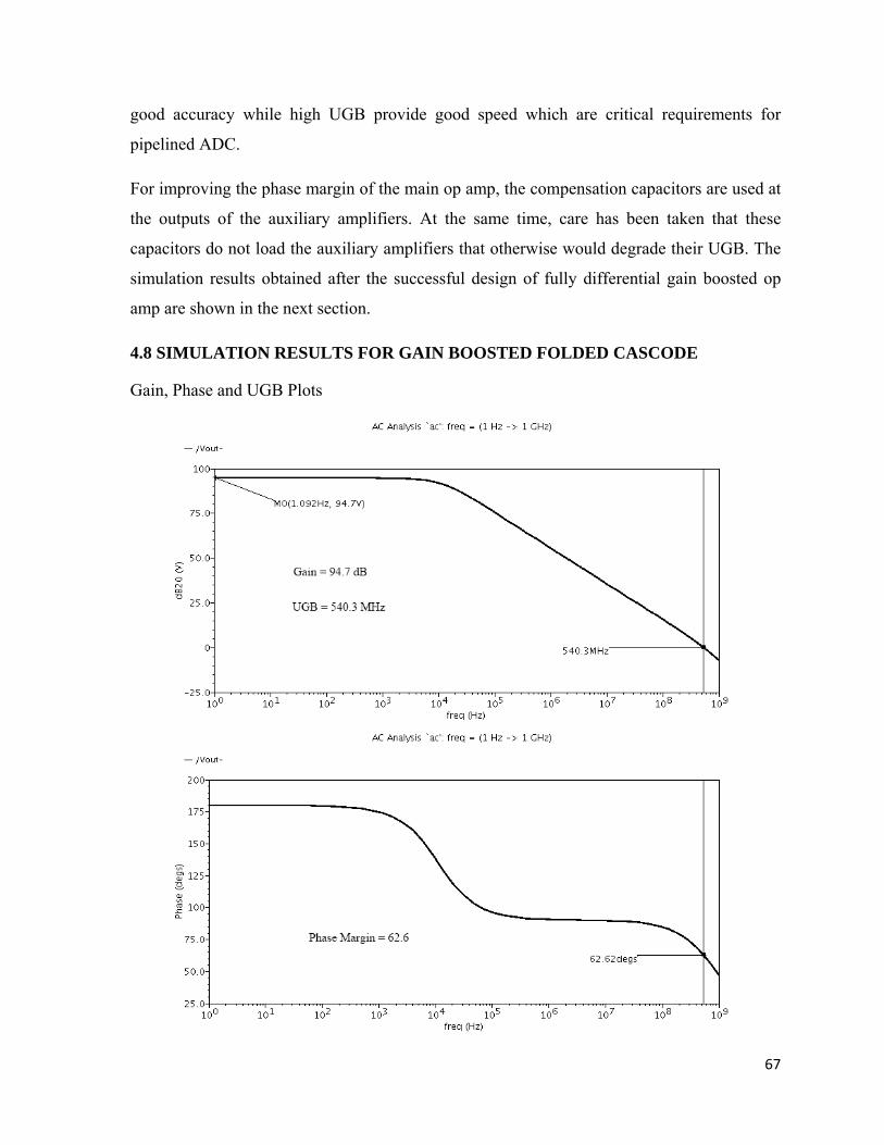
67
good accuracy while high UGB provide good speed which are critical requirements for
pipelined ADC.
For improving the phase margin of the main op amp, the compensation capacitors are used at
the outputs of the auxiliary amplifiers. At the same time, care has been taken that these
capacitors do not load the auxiliary amplifiers that otherwise would degrade their UGB. The
simulation results obtained after the successful design of fully differential gain boosted op
amp are shown in the next section.
4.8 SIMULATION RESULTS FOR GAIN BOOSTED FOLDED CASCODE
Gain, Phase and UGB Plots
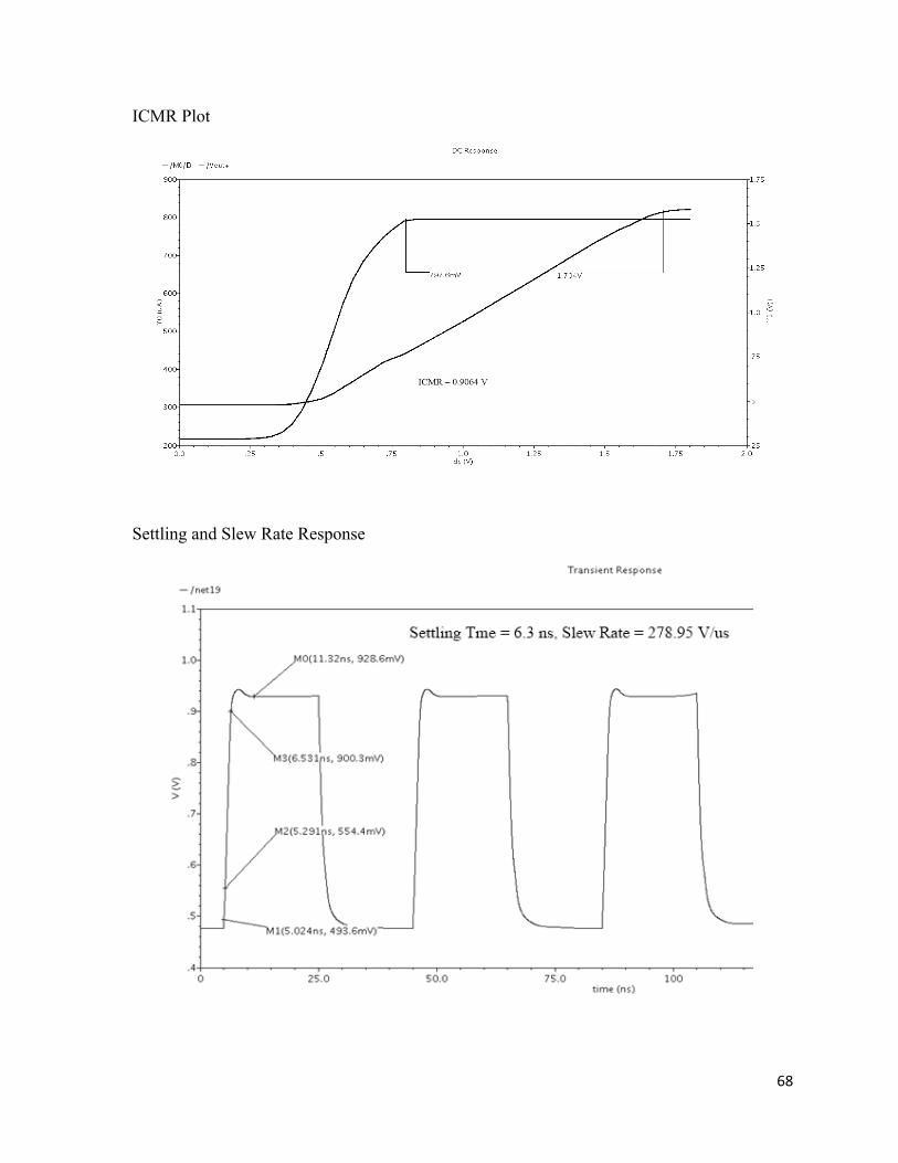
68
ICMR Plot
Settling and Slew Rate Response
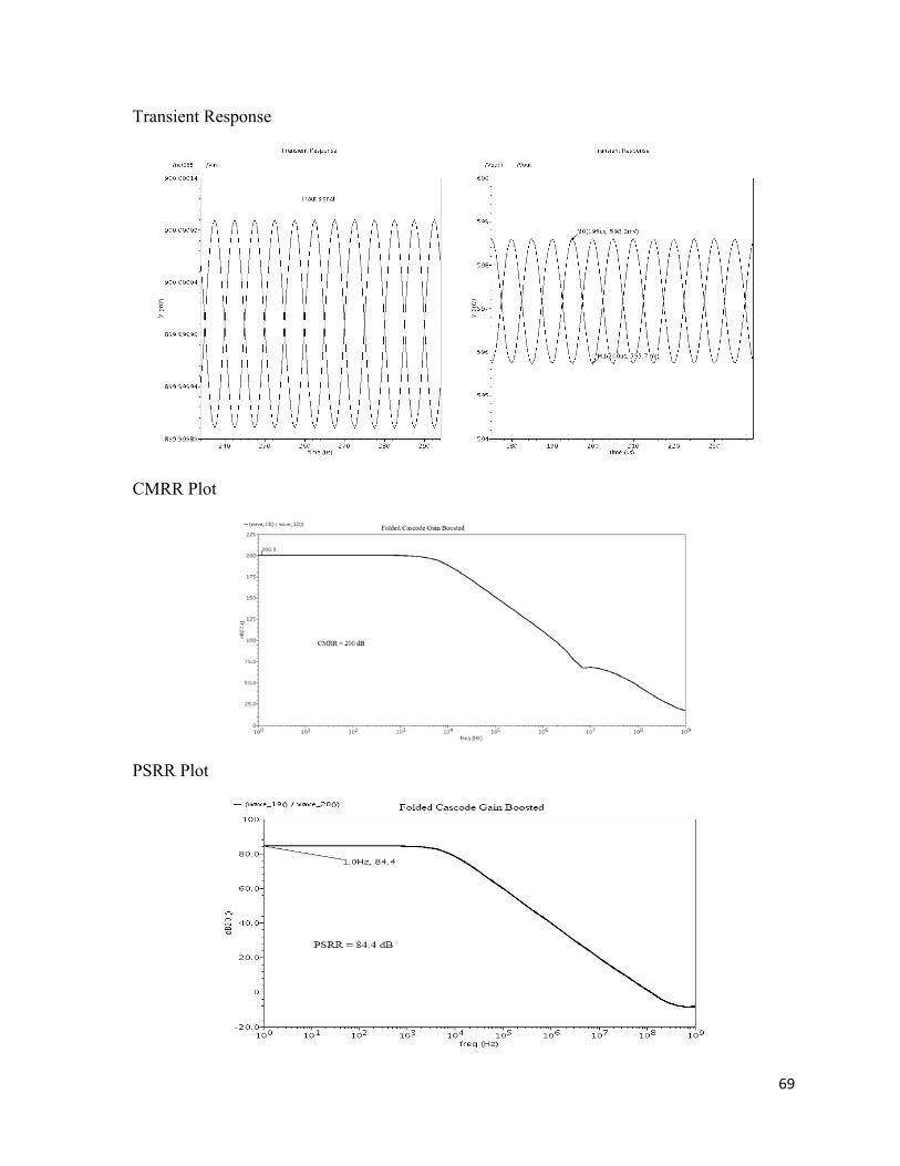
69
Transient Response
CMRR Plot
PSRR Plot
70
CHAPTER 5 LAYOUTS AND POST LAYOUT
SIMULATION Analog layout demand a lot of layout precautions so as to minimize effects such as crosstalk,
mismatches, noise etc. The main problems of layout for analog ICs are device matching and
unwanted parasitic reduction. Sometimes chip area may also be a concern. For matching, the
techniques are common-centroid and interdigititation, which can be used separately or in
combination, as well as dummy devices and device unitization. If there are no parasitic, then
there is no noise coupling. The parasitic reduction techniques include shield, guard ring, long
distance between noisy digital circuitry etc.
5.1 ISSUES IN ANALOG LAYOUT 5.1.1 MATCHING OF DEVICES
Device mismatch is generally treated as part of the black art of analog design. Random
device mismatch plays an important role in the design of accurate analog circuits. The device
mismatch is due to number factors like local process variation, global lithographic variations,
local lithographic variations and process gradients. These factors affect all devices
transistors, resistor, capacitors, and therefore similar techniques can be used to match all
elements.
Matching improves with increasing device area. And accuracy requirements impose a
minimal device area. Use of transistor fingering for large and critical transistors is always
beneficial. In fingering the transistor is “fingered” into multiple transistors that are connected
in parallel. The folded transistors reduce the source/ Drain junction area and the gate
resistance. The gate resistance can be reduced by decomposing the transistor into more
parallel fingers. There is an advantage with an even number of fingers; the active capacitance
is less, because the drain region is surrounded with gate poly instead of field. The large
transistors are broken into number of small transistors in parallel. This also decreases the
physical size of the device, and thus can provide a more compact layout [32].

71
Minimum size will usually provide a minimum in terms of parasitic capacitance, but still this
may not provide the optimal device for a given application. For example, an application that
is more sensitive to gate resistance may warrant a non-optimal device size, in terms of
parasitic capacitance. Lower gate resistance is obtained by smaller finger width. This
increases the overall number of fingers and therefore increases the junction capacitances Csb
and Cdb.
Figure 5.1: Interdigitated MOSFET’s [29]
Since MOSFET’s allow device folding, many devices with the same finger width can be,
“interdigitated” with one another. The only requirement for interdigitating devices is that
these devices share source terminals, drain terminals, or source and drain terminals. These
compact, interdigitated devices provide better matching for both process and thermal
gradients. When matched signals or currents are needed, precision device matching is
required. For example, current mirrors and differential pairs. In many cases, these structures
can provide symmetry along two separate axes, completely alleviating the affects of linear
gradients as shown in figure 5.1. An inter-digitations pattern will minimize source/drain
parasitics by placing two same devices gates back-to-back.

72
While on the subject of matching, it should also be mentioned that metal routing over
transistors might affect device matching. Such routing can cause threshold voltage mismatch
as well as trans-conductance mismatch. Therefore, it is recommended that routing over
transistors be avoided. If such routing cannot be avoided, the routing over symmetric devices
should be made symmetric as well, and if possible, higher metal layers should be used [32].
In order to consistently provide symmetry along two axes, a layout technique called a
“common-centroid” can be used. Figure 5.2 shows how such a layout provides two axes of
symmetry. Typically, this form of layout is used for precise matching of only two devices.
The method can be extended to more devices; however, the routing for such a compound
device becomes very cumbersome.
Figure 5.2: Basic Common Centroid Layout [29] Because each device finger is the same size, this structure provides a very symmetric and
compact layout. Again, the device fingers on the ends of each row are different than the
internal fingers with respect to their surrounding environment, potentially giving rise to
process dependent device variations. The option of using dummy devices will again alleviate
this problem.
The basic idea of dummy devices is to make the device cluster more regular. Etch-rates of
materials can be dependent on the density of the material in a local area. If the material

73
pattern for matched devices is not regular, supposedly identical devices may differ physically
after processing. This mismatch can occur in MOSFETs, resistors, and capacitors.
The final form of MOSFET layout that will be discussed is the cascode. The layout of
the cascode is very similar to that of two interdigitated MOSFET’s. However, in the case of
the cascode, a source and drain are shared between the two devices rather than source or
drain. Since device matching is not the overall goal of the cascode device, symmetry is not as
important as parasitics minimization. Typically, no connection is needed at the terminal
between the devices, therefore no contacts are needed, the device gates can be moved closer
to one another, and the overall device structure can be made smaller.
Figure 5.3 below shows an example of a cascode layout. The most regular cascade
device occurs when both the gain device and the cascode device have the same number of
fingers and the same finger width, as shown in figure 5.1. In many cases, this is not true.
Therefore, not all the devices can be merged, the structure is larger, and parasitic increase.
Figure 5.3: Cascode MOSFET Layout
In summary, MOSFET devices for analog layout usually exist in two forms; those that
require matching and those that do not. For devices that do not require matching, simply
folding the device into smaller fingers creates a smaller layout and reduces some device
parasitics (gate resistance and source/drain to bulk capacitances). For devices that do require

74
matching, current mirrors, differential pairs, etc., each device is broken up into fingers of the
same width, which are interdigitated together to form a compound device. Usually, for two
devices of the same size that share a source or drain, a common-centroid layout with dummy
devices is used. If more devices must be matched, an interdigitation pattern with dummy
devices is used. There are many other ways to create a MOSFET in layout that are very
application specific. For example, power transistor layouts will be quite different from any of
the above layouts because of the amount of current that power devices must source [32].
5.1.2 NOISE ISSUE IN LAYOUT DESIGN
Noise is important in all analog circuits because it limits dynamic range. In general there are
two types of noise, random noise and environmental noise. Random noise refers to noise
generated by resistors and active devices in an integrated circuit; environmental noise refers
to unwanted signals that are generated by humans. Two common examples of environmental
noise are switching of digital circuits and 60 Hz 'hum'. In general, random noise is dealt with
at the circuit design level. However the are some layout techniques which can help to reduce
random noise. multi-gate finger layout reduces the gate resistance of the poly-silicon and the
neutral body region, which are both random noise sources. Generous use of substrate plugs
will help to reduce the resistance of the neutral body region, and thus will minimize the noise
contributed by this resistance.
Multi-gate finger layout refers to implementing a single, wide transistor as several
narrow transistors in parallel. This minimizes the gate resistance and it also makes it easier to
match the transistor with other devices. Use of transistor fingering for large and critical
transistors is always beneficial. In fingering the transistor is “fingered” into multiple
transistors that are connected in parallel. The folded transistors reduce the source/ Drain
junction area and the gate resistance. The gate resistance can be reduced by decomposing the
transistor into more parallel fingers. There is an advantage with an even number of fingers;
the active capacitance is less, because the drain region is surrounded with gate poly instead of
field
The layouts in this section are designed using multi-gate finger with interdigitition
technique and the number of fingers are kept even with all finger widths <= 15µm.
followings are the layouts of all designed op amps whose LVS have been successfully
matched.

75
5.3 LAYOUT DESIGNS WITH LVS MATCHED
Layouts of all designed op amp have been designed in Cadence Virtuoso. Following steps have been
performed successfully while layout designs:
1. DRC Run
2. LVS Run
3. RCX Run
Followings are the layout of each op amp designed in this thesis work:
5.3.1 LAYOUT OF SINGLE ENDED SIMPLE TWO STAGE OP AMP
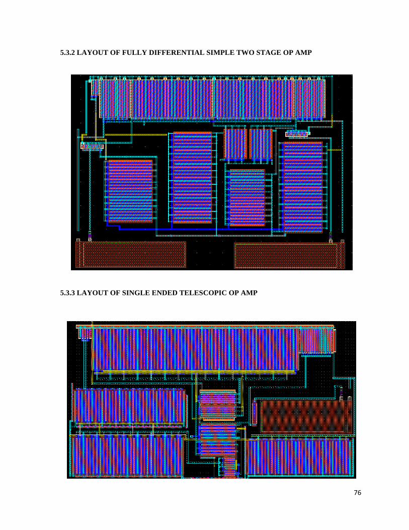
76
5.3.2 LAYOUT OF FULLY DIFFERENTIAL SIMPLE TWO STAGE OP AMP
5.3.3 LAYOUT OF SINGLE ENDED TELESCOPIC OP AMP
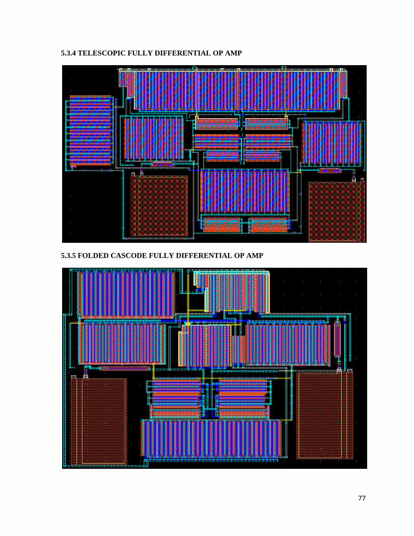
77
5.3.4 TELESCOPIC FULLY DIFFERENTIAL OP AMP
5.3.5 FOLDED CASCODE FULLY DIFFERENTIAL OP AMP
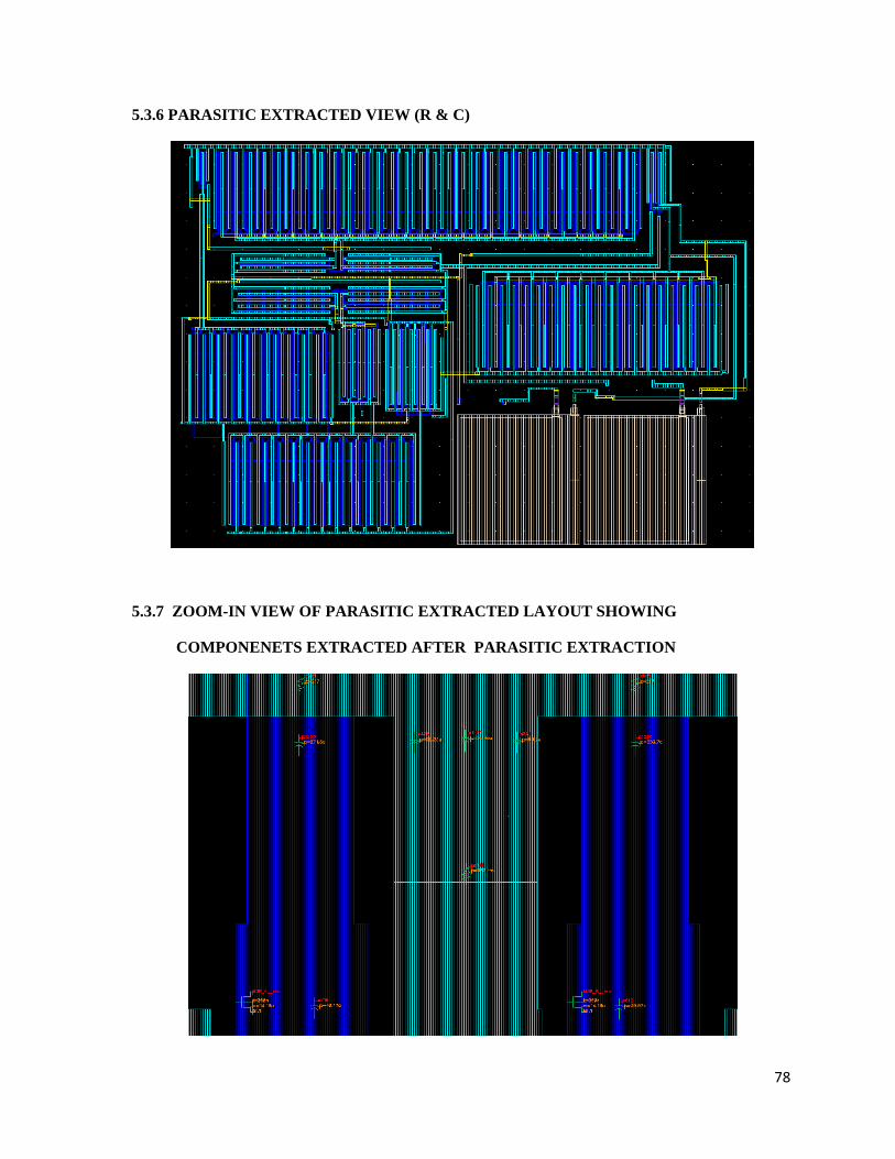
78
5.3.6 PARASITIC EXTRACTED VIEW (R & C)
5.3.7 ZOOM-IN VIEW OF PARASITIC EXTRACTED LAYOUT SHOWING
COMPONENETS EXTRACTED AFTER PARASITIC EXTRACTION
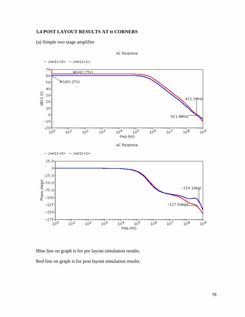
79
5.4 POST LAYOUT RESULTS AT tt CORNERS
(a) Simple two stage amplifier
Blue line on graph is for pre layout simulation results.
Red line on graph is for post layout simulation results.

80
(b) Telescopic Amplifier
Blue line on graph is for post layout simulation results.
Red line on graph is for pre layout simulation results
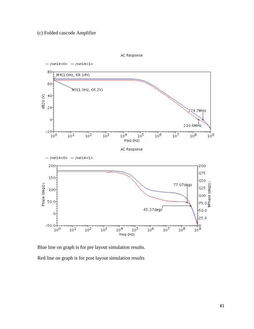
81
(c) Folded cascode Amplifier
Blue line on graph is for pre layout simulation results.
Red line on graph is for post layout simulation results
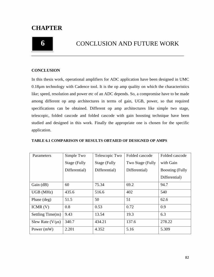
82
CHAPTER 6 CONCLUSION AND FUTURE WORK
CONCLUSION
In this thesis work, operational amplifiers for ADC application have been designed in UMC
0.18µm technology with Cadence tool. It is the op amp quality on which the characteristics
like; speed, resolution and power etc of an ADC depends. So, a compromise have to be made
among different op amp architectures in terms of gain, UGB, power, so that required
specifications can be obtained. Different op amp architectures like simple two stage,
telescopic, folded cascode and folded cascode with gain boosting technique have been
studied and designed in this work. Finally the appropriate one is chosen for the specific
application.
TABLE 6.1 COMPARISON OF RESULTS OBTAIED OF DESIGNED OP AMPS
Parameters Simple Two
Stage (Fully
Differential)
Telescopic Two
Stage (Fully
Differential)
Folded cascode
Two Stage (Fully
Differential)
Folded cascode
with Gain
Boosting (Fully
Differential)
Gain (dB) 60 75.34 69.2 94.7
UGB (MHz) 435.6 516.6 402 540
Phase (deg) 51.5 50 51 62.6
ICMR (V) 0.8 0.53 0.72 0.9
Settling Time(ns) 9.43 13.54 19.3 6.3
Slew Rate (V/µs) 340.7 434.21 137.6 278.22
Power (mW) 2.201 4.352 5.16 5.309
83
Simple two stage op amp designed in this work fulfills the requirement for unity gain buffer.
The telescopic amplifier has been designed which meets the specifications for the sample and
hold architecture and MDAC unit of targeted pipelined ADC. Folded cascode amplifier has
been also designed for the MDAC unit but due to some design problems, its performance is
not as better as is obtained in telescopic architecture. So, finally telescopic architecture is
chosen for MDAC section of pipelined ADC.
Folded cascode op amp with gain boosting technique was designed to find the further
improvement in the op amp design without degrading its speed. So, a fully differential folded
cascode op amp with gain boosting technique has been designed. This op amp may be used
for 8-14 bits 100MSPS pipelined ADC.
Layout of simple two stage, telescopic and folded cascode op amp has been designed in
Cadence Virtuoso. Layout vs. Schematic (LVS) check has been performed successfully using
Assura. Parasitic extraction has been done and post layout simulations are performed at tt
corners. Pre layout and post layout results differ due to prasitics (R and C) of different layers
in layout.
Complete corner simulations need to be make successful for the robust design, which are still
to be performed for all designs. Due to lack of time all, process corner simulation were not
performed. But during the design period process corner variations were kept in mind and
hence enough margins were chosen for each design. So, it is expected that there will not be
much problem during process corner simulations.
FUTURE SCOPE
In this thesis work only operational amplifiers were designed for pipelined ADC. Op amp is
the most critical part of such design which is grasped well during this work. In future there
may be a target to design the complete fully differential pipelined ADC which meets the
modern high speed requirements.

84
APPENDIX A TECHNOLOGY PARAMETERS
AND CAD TOOLS
Following is the technology parameters for designing and CAD tools used in this thesis work
in the design and verification.
TECHNOLOGY PARAMETERS
Foundry Spec. : UMC 0.18um twin-tub CMOS 1P6M process
Voltage range : 0V-1.8V
SPICE Models : BSIM3v3 (Level 49)
CAD TOOLS
Schematic Entry : Cadence Schematic Entry Analog Design Environment
Simulator : Cadence SPECTRE
Layout : Cadence Virtuoso
Verification : Mentor Graphic’s Calibre for DRC/LVS
Extraction : Mentor Graphic’s XRC Extraction tool.

85
REFERENCES
[1] Phillip E. Allen, Douglas R. Holberg, “CMOS Analog Circuit Design,” Textbook,
Oxford University Press, Second Edition 2007.
[2] Behzad Razavi, “Design of Analog CMOS Integrated Circuits,” Tata McGraw-Hill
Edition 2002.
[3] Shailesh B.Nerurkar and Khalid H. Abed, “CMOS Fully Differential Operational
Transconductance Amplifier Delta-Sigma Modulators”, IEEE Journals of Solid State
Circuits, vol.1, 2008.
[4] Liang Shang-Quan, Yin Yong-Sheng, Deng Hong-Hui, Song Yu-Kun And Gao
Ming-Lun, “A Low Power Consumption, High Speed Op-amp for a 10-bit 100MSPS
Parallel Pipeline ADC”, IEEE, Circuits and Systems, 2008
[5] D. Meganathan, Amrith Sukumarn, M.M. Dinesh Babu, S. Moorthi, A Systematic
Design Approach for Low-Power 10-bit 100MS/s Pipelined ADC, Microelectronics
Journal, 2009.
[6] Eri Perasetyo, Dominique Ginhac, Michel Paindavoine, “ Design and Implementation
of 8 bits Pipelined Analog to Digital Converter in the Technology 0.6µm CMOS
Process”, Computing Research Repository - CORR, 2008.
[7] Jirayuth Mahattanakul, “Design Procedure for Two Stage CMOS Opamp with
Flexible Nosie –Power Balancing Scheme”. IEEE Transcations on Circuits and
Systems-I, vol. 52, 2005.
[8] Grayson King,“ Application Note-OP AMPS Driving the capacitive Load” Analog
Dialogue, 1997.
[9] Andrew M. Abo and Paul R. Gray “A 1.5-V, 10-bit, 14.3-MS/s CMOS Pipeline
Analog-to-Digital Converter”, IEEE Journal of Solid-State Circuits, Vol. 34, no. 5,
May 1999.
[10] R. Jacob Baker, “CMOS: Circuit Design, Layout, and Simulation”, IEEE series on
Microelectronics system, IEEE press, Wiley Publication, 2010.
86
[11] Allen Y Chen and Pavel Monat, “A Fully Differential Two Stage CMOS Operational
Amplifier”, Term Paper, Spring 2003.
[12] Gray, Hurst, Analysis and Design Analog Integrated Circuits, Lewis & Mayer, John
Wiley & Sons, Fourth edition.
[13] J. Mahattanakul, “Design Procedure for Two-Stage CMOS Operational Amplifiers
Employing Current Buffer”, IEEE Transactions On Circuits And Systems-II: Express
Briefs, Vol. 52, November 2005.
[14] G. Palmisano and G. Palumbo,” A Compensation Strategy for Two-Stage CMOS
Opamps Based on Current Buffer”, IEEE Transactions On Circuits and Systems-I:
Fundamental Theory And Applications, vol. 44, March 1997.
[15] Fred Chen, Kevin Yang, “A Fully Differential CMOS TelescopicOperational
Amplifier with Class AB Output Stage”, Project Report, 1999.
[16] Donny Mota, “Fundamentals of Fully Differential Op-Amps and CMFB Circuit
Design”, Term Paper, Advanced Topics in Analog Circuits, 2001.
[17] Yun Chiu, Ken Wojciechowski, “A Gain-Boosted 90-dB Dynamic Range Fast
Settling OTA with 7.8-mW Power Consumption”, Electrical Engineering and
Computer Science Department University of California, Berkeley, 2004.
[18] A. Chang and D. Fang, A Low Power, Two Stage Telescopic Amplifier with 80 dB
Dynamic Range And 10 ns Settling Time, Design project, Spring 2007.
[19] David A Johns, Ken Martin, “Analog Integrated Circuit Design”, John Wiley and
Sons Inc, Copyright 1997.
[20] RichardE, Valle and Ezz El Masry, “A Very High-Frequency CMOS Complementary
Folded Cascode Amplifier,” IEEE Journals of Solid State Circuits, vol. 29, No. 2,
1994.
[21] Katsufumi Nakamura and L. Richard Carley, “An Enhanced Fully Differential
Folded-Cascode Op Amp,” IEEE Journals of Solid State Circuits, vol. 27, No. 4, pp
563-568, 1992.
[22] A. R. Mortazavi, M. R. Hassanzadeh, J. Talebzadeh, and O. Shoaei, “Design
Procedure for a High C-Gain and High- Bandwidth Amplifier,” Master of Science
Thesis, University of Tehran, Iran, 2001.

87
[23] D. Miyazaki, “ A 10 b 30-MS/s Low Power Pipelined CMOS A/D Converter Using
Pseudo differential Architecture”, IEEE Journals of Solid State Circuits,vol.38, No.2,
2003.
[24] T. Lehmann and M. Cassia, “1-V Power Supply CMOS Cascode Amplifier,” IEEE
Journals of Solid State Circuits, vol. 36, No. 7, 2001.
[25] Wen-Whe Sue, Zhi-Ming Lin, and Chou-Hai Huang, “A High DC-Gain Folded-
Cascode CMOS Operational Amplifier,” IEEE Journals of Solid State Circuits, vol
78, No. 3, 1998
[26] Eduaed Suckiger, Walter Guggenbuhl, “A High-Swing, High-Impedance MOS
Cascode Circuit”, IEEE Journal Of Solid-State Circuits, Vol. SC-25, No. 1, February
1990.
[27] Ashish C Vora, “Operational Transconductance Amplifier (OTA) Using Gain
Boosting Technique”, Master’s Thesis, Department Of Electrical Engineering Kate
Gleason College Of Engineering Rochester Institute Of Technology Rochester, New
York December 2005.
[28] Weibiao Zhang, Marwan Hassoun, “A Small Signal Analysis of a Gain Boosting
Amplifier”, IEEE, Southwest Symposium on Mixed-Signal Design, 2000.
[29] Mezbah Uddin Shaber, Svante Signell, “Fully Differential Gain-Boosted OTA Design
for Pipeline Daconverter in 180nm CMOS Technology”, IEEE, Electronics, Circuits
and Systems, 2005.
[30] A. Halim El-Saadi, Mohammed El-Tanani, “A High Speed Operational Amplifier”,
University of Michigan, EECS413, Final project, 2007.
[31] M. Di Ciano, C. Marzoccal, A. Tauro, “A low voltage, high output impedance CMOS
current source”, IEEE, Semiconductor Electronics, 2004. ICSE 2004.
[32] Patrick T. McElwee, “An Automated Analog Layout Generation Flow,” Term Paper,
University of California, Berkely, 2005.
.