design of high-speed laser driver using a standard cmos technology for optical data transmission...
TRANSCRIPT
Design of High-Speed Laser Driver Using a Standard CMOS Technology for Optical Data Transmission
Dissertation Defense Presentation
By
Seok Hun Hyun
Advisor: Martin A. Brooke
November 2004
Outline Introduction
Background
Design of A High Current Laser Driver
Design of A Low Power Laser Driver
Thin Film Laser Integration onto CMOS circuits
Conclusion and Future Research
Introduction Objective
Design of laser driver for optical data transmission
Using a standard CMOS technology
Studying the behavior of circuit performance with parasitic components
Working at commercially interesting high-speed and low power consumption
Introduction Fundamental constraints in electronic
communication links
Noise, Interference, Power, Cost, etc.
Use of optics as a replacement for electronics
LAN, MAN, board-to-board and chip-to-chip interconnects
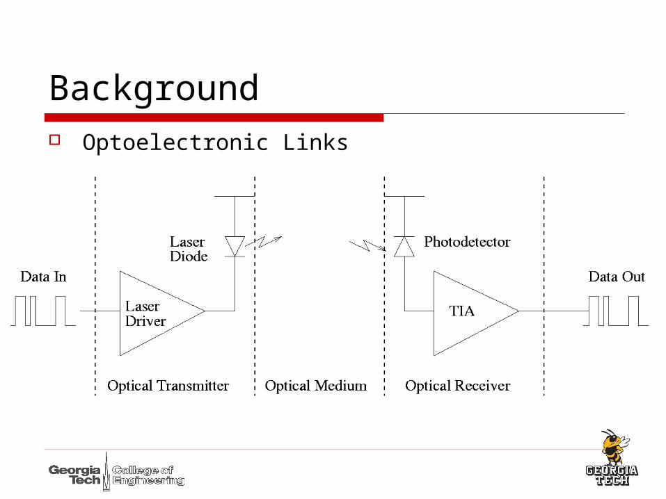
Background Optoelectronic Links
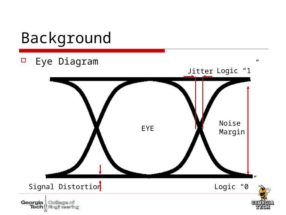
Background Eye Diagram
EYENoiseMargin
Logic “1”
Logic “0”
Jitter
Signal Distortion
Background CMOS technology
Low power
Low cost
High yield
Higher degree of integration
Vast standard cell library
TSMC 0.18 um mixed-signal CMOS
Background Laser Driver
The electro-optic interface limits the maximum speed of system
Simple current switch responses to the input signal modulated with data stream
Critical challenge: To deliver large current with very short rise and fall times since the bandwidth is trade off for large current.
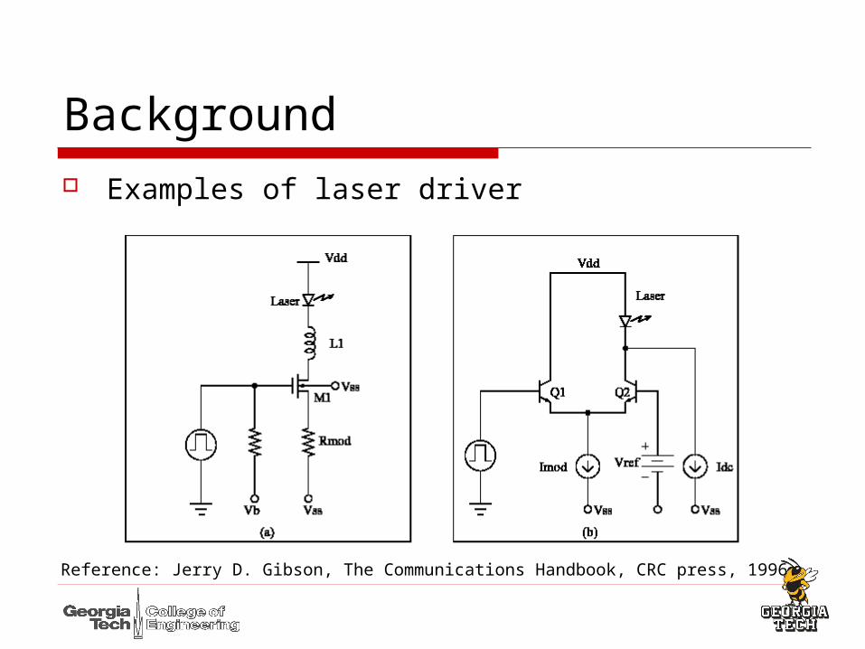
Background Examples of laser driver
Reference: Jerry D. Gibson, The Communications Handbook, CRC press, 1996.

High Current Laser Driver
Required to be other types of lasers FP, DFB, MQW, etc.
More than 20 mA modulation currents
A driver for LVDS standards Input: 100 mVp-p
Speed : > 10 Gbps Output current: Mod. 0~40 mA, Bias : 0~30 mA
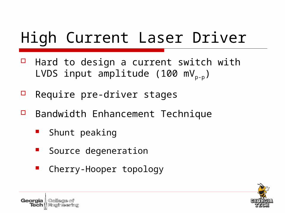
High Current Laser Driver Hard to design a current switch with LVDS input
amplitude (100 mVp-p)
Require pre-driver stages
Bandwidth Enhancement Technique
Shunt peaking
Source degeneration
Cherry-Hooper topology
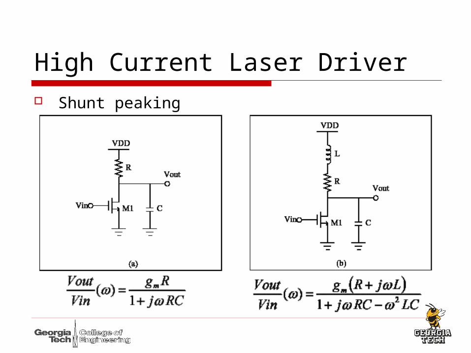
High Current Laser Driver Shunt peaking
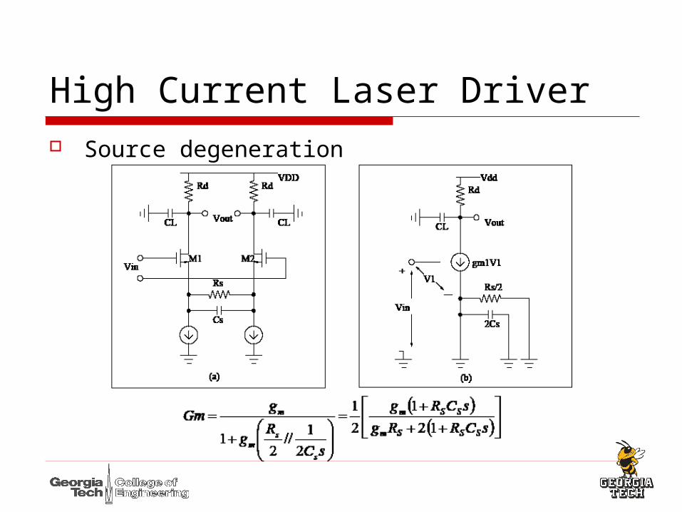
High Current Laser Driver Source degeneration
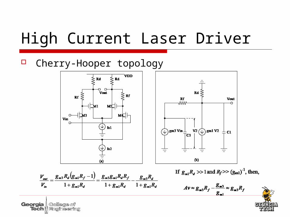
High Current Laser Driver Cherry-Hooper topology
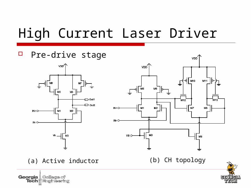
High Current Laser Driver Pre-drive stage
(a) Active inductor (b) CH topology
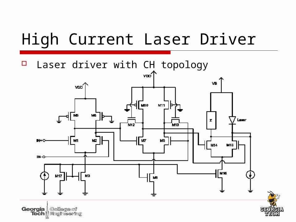
High Current Laser Driver Laser driver with CH topology

High Current Laser Driver Eye diagram at 10 Gbps
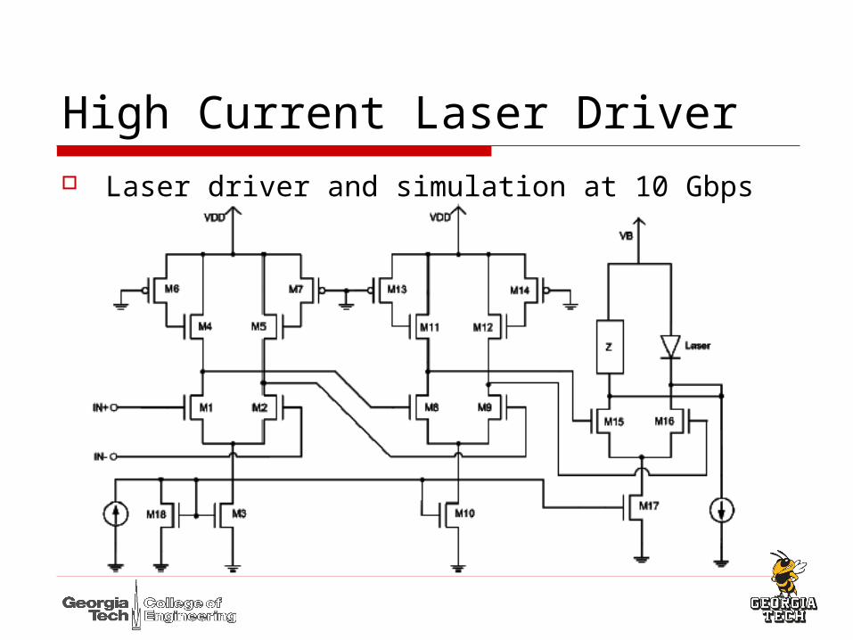
High Current Laser Driver Laser driver and simulation at 10 Gbps

High Current Laser Driver Eye diagram at 10 Gbps
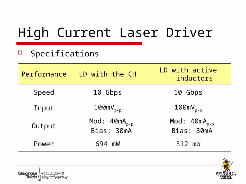
High Current Laser Driver Specifications
Performance LD with the CHLD with active
inductors
Speed 10 Gbps 10 Gbps
Input 100mVp-p 100mVp-p
OutputMod: 40mAp-p
Bias: 30mAMod: 40mAp-p
Bias: 30mA
Power 694 mW 312 mW
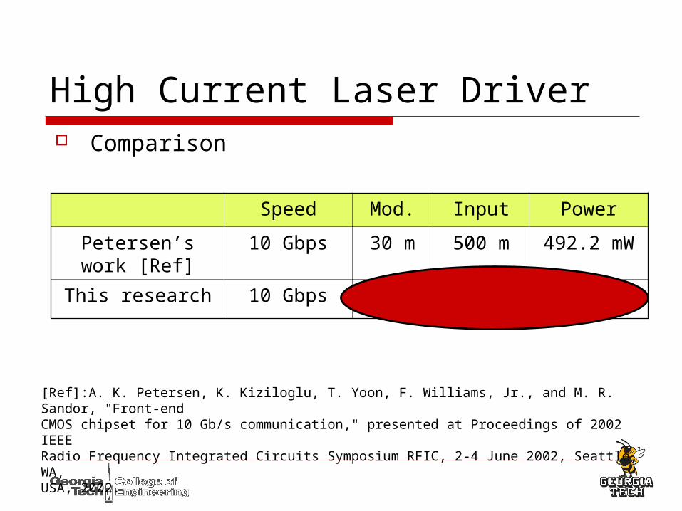
High Current Laser Driver
Speed Mod. Input Power
Petersen’s work [Ref]
10 Gbps 30 m 500 m 492.2 mW
This research 10 Gbps 40 m 100 m 312 mW
Comparison
[Ref]:A. K. Petersen, K. Kiziloglu, T. Yoon, F. Williams, Jr., and M. R. Sandor, "Front-endCMOS chipset for 10 Gb/s communication," presented at Proceedings of 2002 IEEERadio Frequency Integrated Circuits Symposium RFIC, 2-4 June 2002, Seattle, WA,USA, 2002.
Low Power CMOS Laser Driver Parallel Optical Interconnects (POI) are
available for rack-to-rack communication at bandwidth of up to 30 Gbps with 12 channels of 2.5 Gbps operation
Next generation POIs will operate at 10 Gbps
The key to demonstrate such links is low power laser driver and receiver
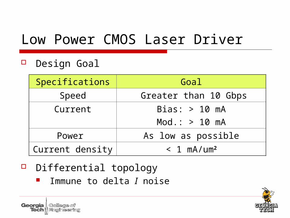
Low Power CMOS Laser Driver
Design Goal
Differential topology Immune to delta I noise
Specifications Goal
Speed Greater than 10 Gbps
Current Bias: > 10 mAMod.: > 10 mA
Power As low as possible
Current density < 1 mA/um2
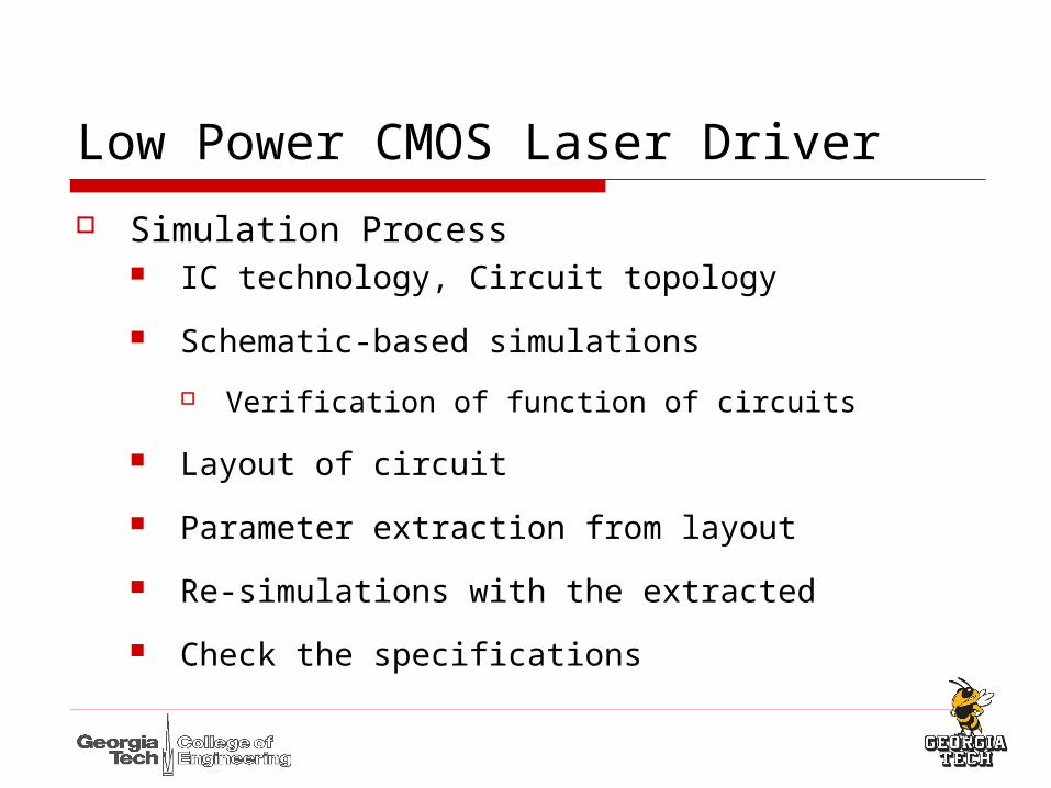
Low Power CMOS Laser Driver
Simulation Process IC technology, Circuit topology
Schematic-based simulations
Verification of function of circuits
Layout of circuit
Parameter extraction from layout
Re-simulations with the extracted
Check the specifications
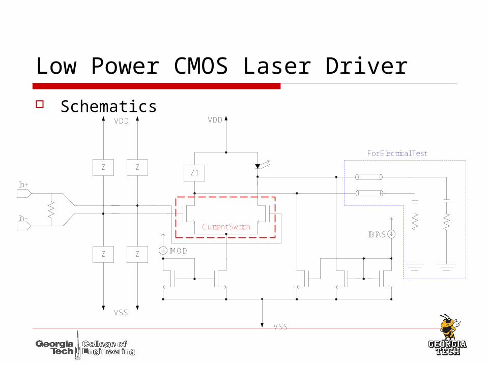
Low Power CMOS Laser Driver
Schematics
In+
In-
Z
VDD VDD
VSS
IMOD
IBIAS
For Electrical Test
Current Switch
Z
Z
Z
VSS
Z1
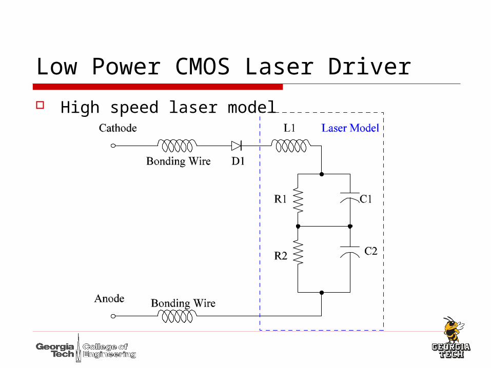
Low Power CMOS Laser Driver
High speed laser model
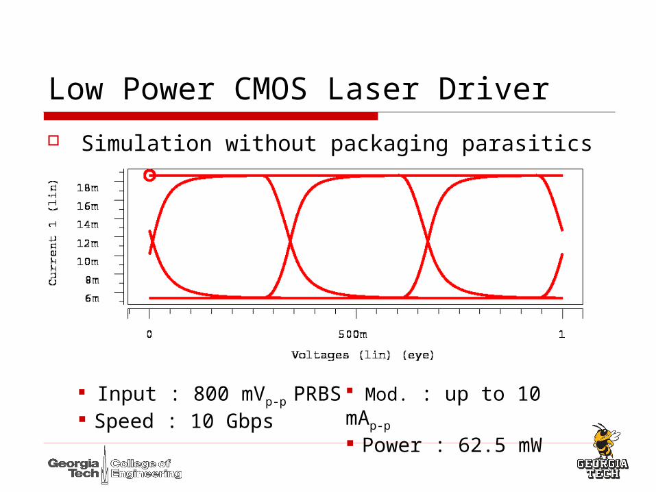
Low Power CMOS Laser Driver
Simulation without packaging parasitics
Input : 800 mVp-p PRBS Speed : 10 Gbps
Mod. : up to 10 mAp-p
Power : 62.5 mW

Low Power CMOS Laser Driver Simulation with packaging parasitics
Wire-bonding parasitics Traces on test board Soldering and cable
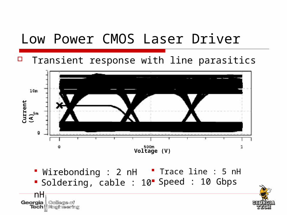
Low Power CMOS Laser Driver Transient response with line parasitics
Cu
rren
t (A
)
Voltage (V)
Wirebonding : 2 nH Soldering, cable : 10 nH
Trace line : 5 nH Speed : 10 Gbps
Low Power CMOS Laser Driver
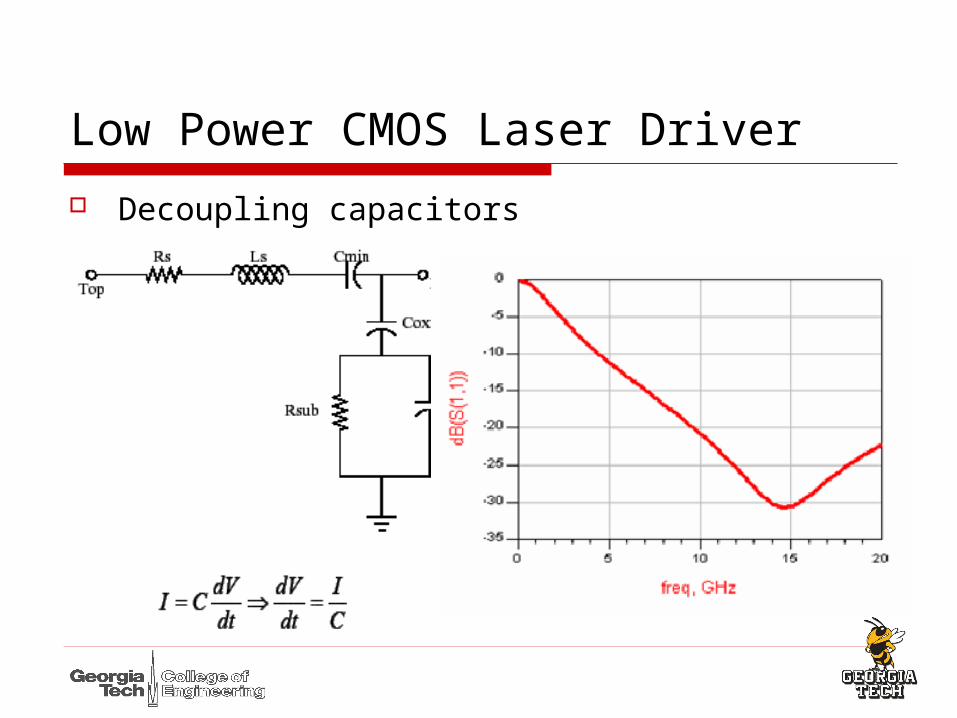
Decoupling capacitors
Low Power CMOS Laser Driver
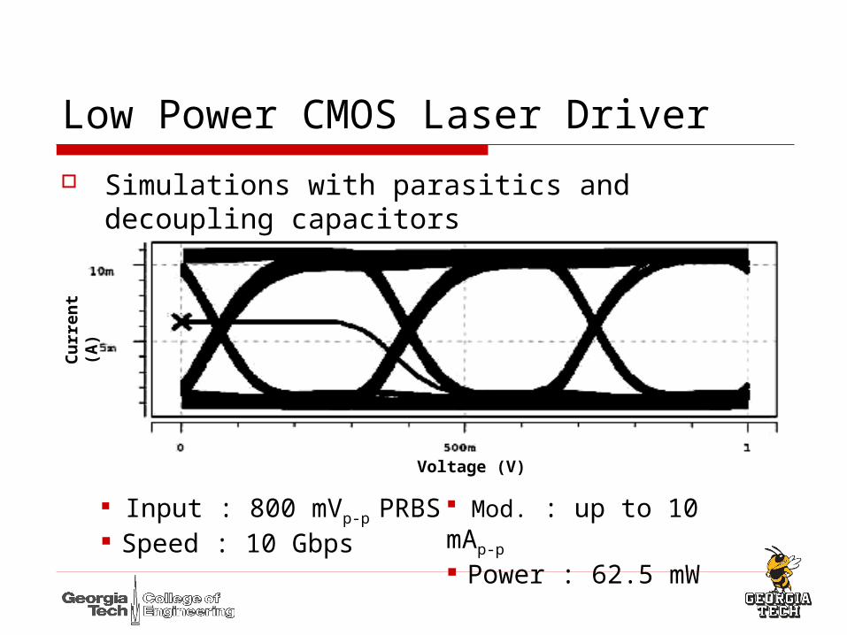
Simulations with parasitics and decoupling capacitors
Cu
rren
t (A
)
Voltage (V)
Input : 800 mVp-p PRBS Speed : 10 Gbps
Mod. : up to 10 mAp-p
Power : 62.5 mW
Low Power CMOS Laser Driver
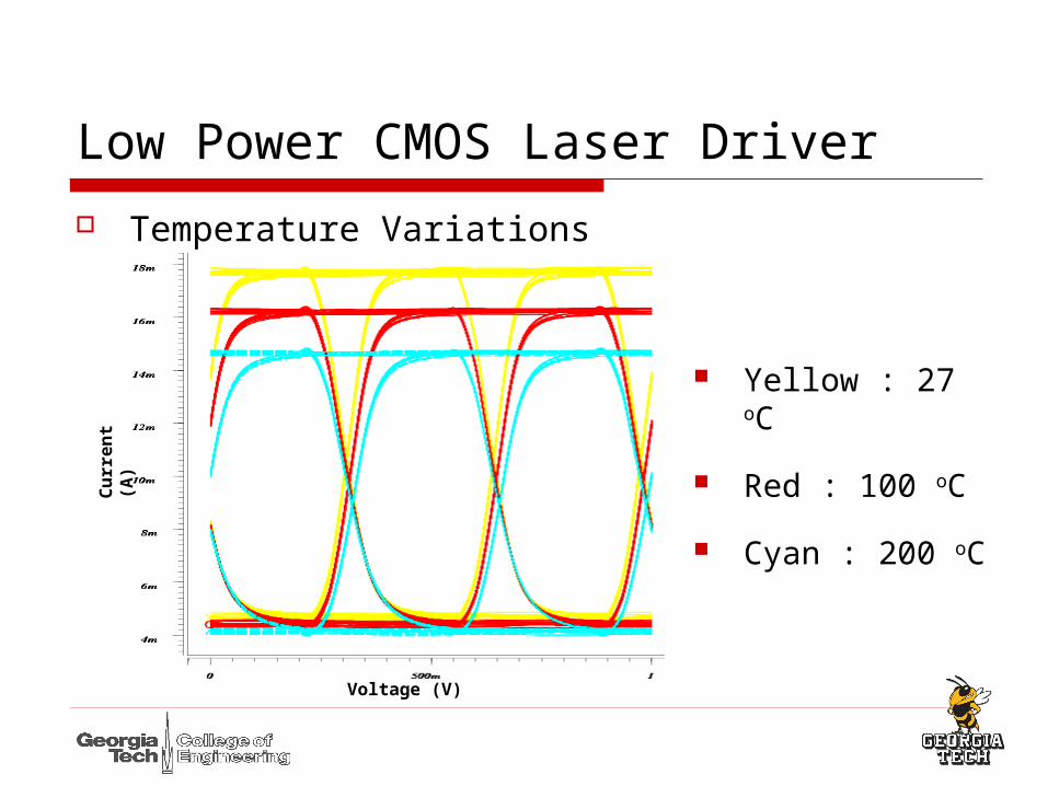
Temperature Variations
Yellow : 27 oC
Red : 100 oC
Cyan : 200 oC
Voltage (V)
Cu
rren
t (A
)
Low Power CMOS Laser Driver
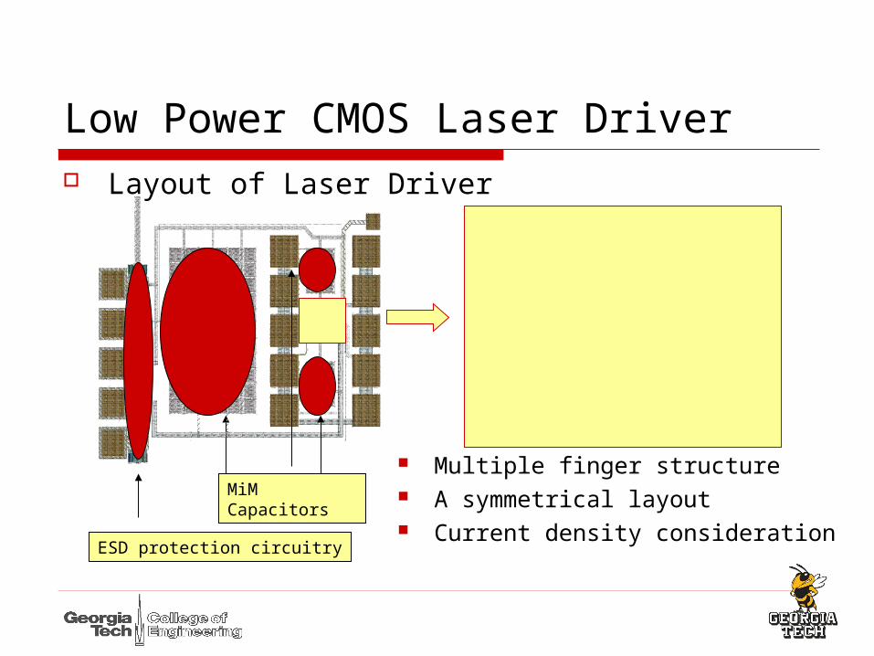
ESD protection circuitry
MiM Capacitors
Multiple finger structure A symmetrical layout Current density consideration
Layout of Laser Driver

Low Power CMOS Laser Driver
Transimpedance amplifier
Laser Drivers Calibration transistors
TSMC 0.18um Chip Layout

Low Power CMOS Laser Driver
Positive ESD Pulse are clamped to the ESD_VDD
Negative ESD pulse are clamped to the ESD_VSS
ESD protection circuitry
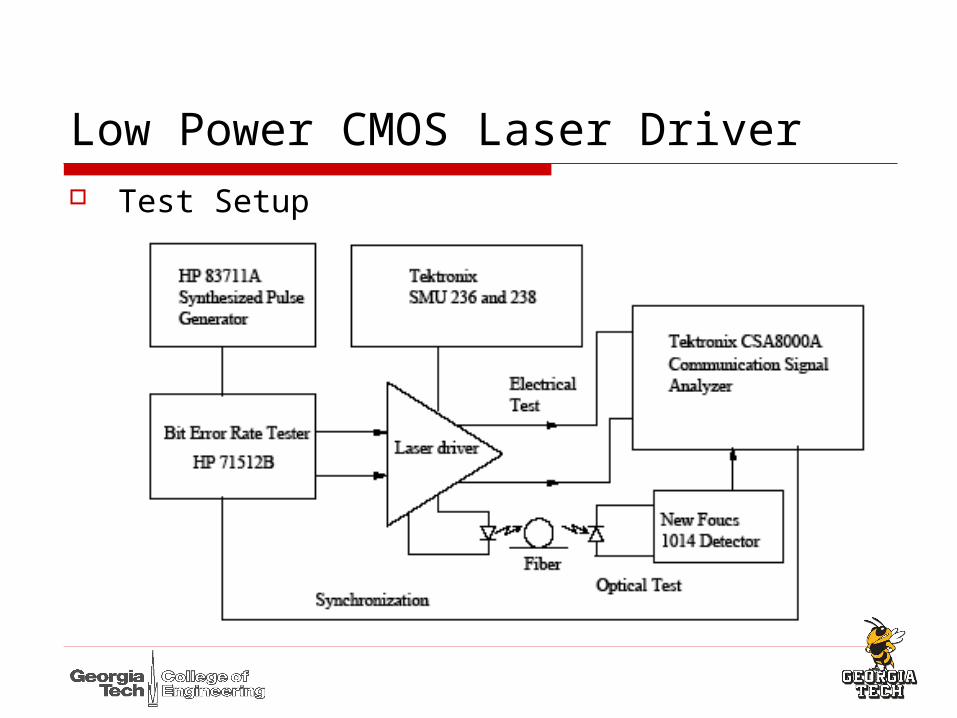
Low Power CMOS Laser Driver Test Setup
Low Power CMOS Laser Driver
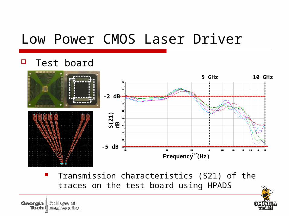
Test board
Transmission characteristics (S21) of the traces on the test board using HPADS
Frequency (Hz)
S(2
1)
dB
5 GHz 10 GHz
-5 dB
-2 dB
Low Power CMOS Laser Driver
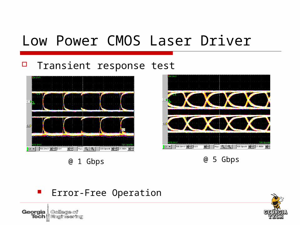
Transient response test
@ 1 Gbps
Error-Free Operation
@ 5 Gbps

Low Power CMOS Laser Driver
Transient response test
3.11 x 10 -14 BER at 10 Gbps
@ 10 Gbps @ 12 Gbps
Low Power CMOS Laser Driver
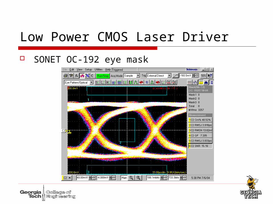
SONET OC-192 eye mask
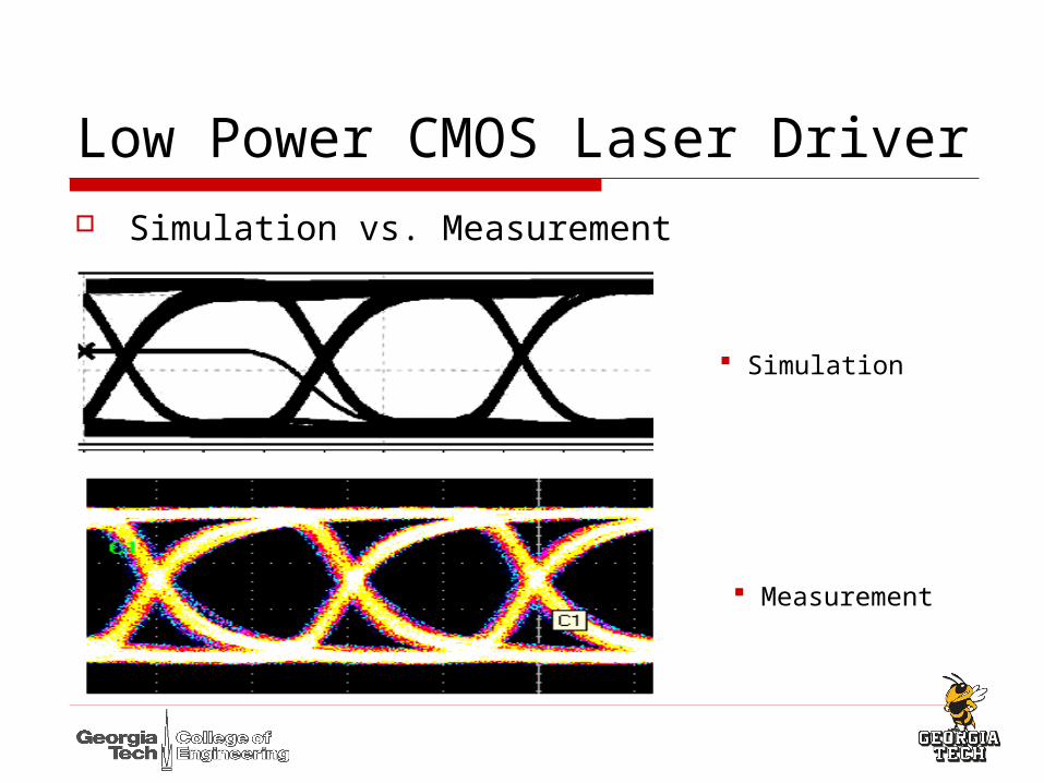
Low Power CMOS Laser Driver Simulation vs. Measurement
Simulation
Measurement
Low Power CMOS Laser Driver
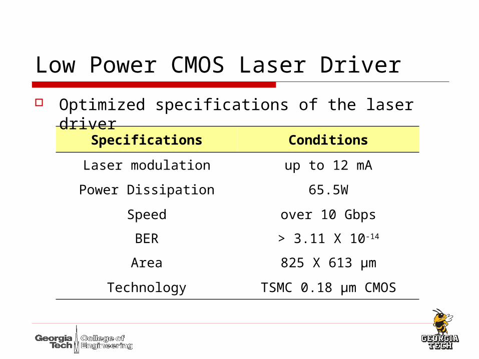
Specifications Conditions
Laser modulation up to 12 mA
Power Dissipation 65.5W
Speed over 10 Gbps
BER > 3.11 X 10⁻¹⁴
Area 825 X 613 μm
Technology TSMC 0.18 μm CMOS
Optimized specifications of the laser driver
Low Power CMOS Laser Driver
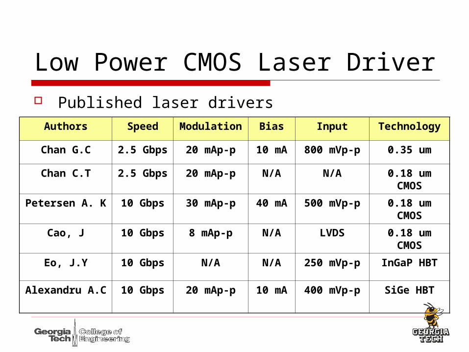
Authors Speed Modulation
Bias Input Technology
Chan G.C 2.5 Gbps 20 mAp-p 10 mA 800 mVp-p 0.35 um
Chan C.T 2.5 Gbps 20 mAp-p N/A N/A 0.18 um CMOS
Petersen A. K 10 Gbps 30 mAp-p 40 mA 500 mVp-p 0.18 um CMOS
Cao, J 10 Gbps 8 mAp-p N/A LVDS 0.18 um CMOS
Eo, J.Y 10 Gbps N/A N/A 250 mVp-p InGaP HBT
Alexandru A.C 10 Gbps 20 mAp-p 10 mA 400 mVp-p SiGe HBT
Published laser drivers
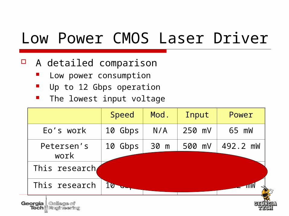
Low Power CMOS Laser Driver A detailed comparison
Low power consumption Up to 12 Gbps operation The lowest input voltage
Speed Mod. Input Power
Eo’s work 10 Gbps N/A 250 mV 65 mW
Petersen’s work 10 Gbps 30 m 500 mV 492.2 mW
This research 12 Gbps 10 m 800 mV 65.5 mW
This research 10 Gbps 40 m 100 mV 312 mW
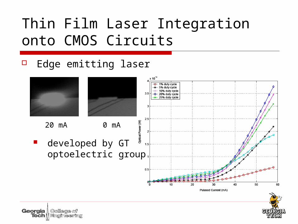
Thin Film Laser Integration onto CMOS Circuits
20 mA 0 mA
developed by GT optoelectric group
Edge emitting laser

Thin Film Laser Integration onto CMOS Circuits
Thin film integration
Separate fabrication
Independent optimization
Reduce packaging parasitics
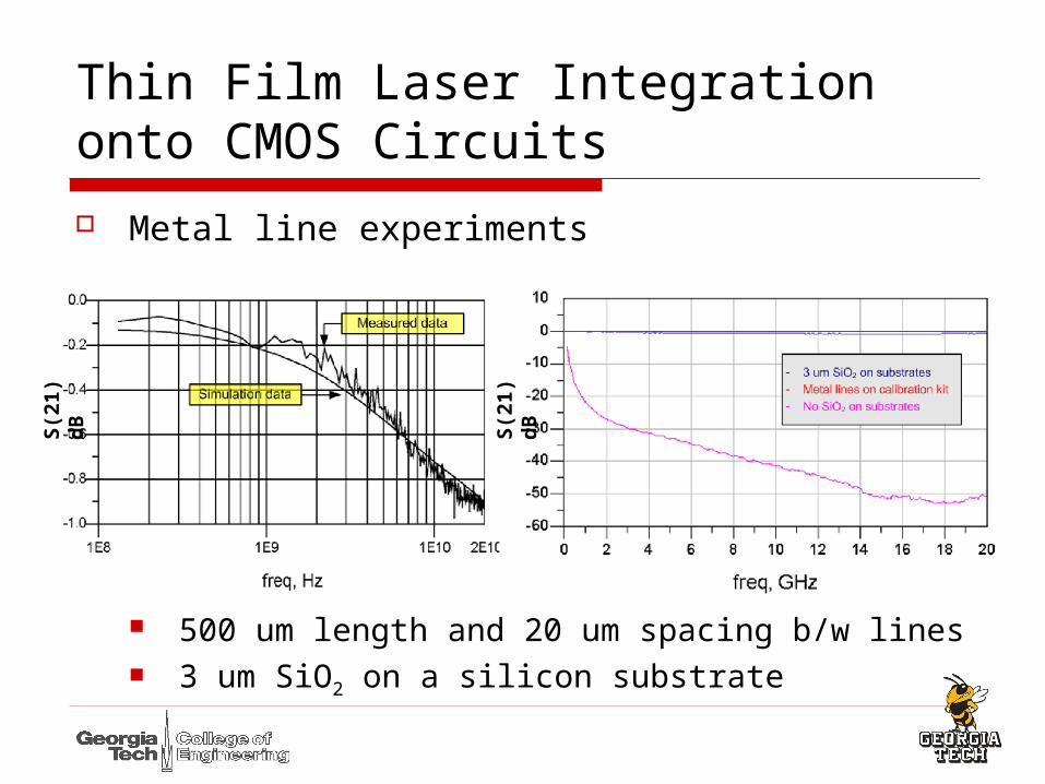
Thin Film Laser Integration onto CMOS Circuits
Metal line experiments
500 um length and 20 um spacing b/w lines 3 um SiO2 on a silicon substrate
S(2
1)
dB
S(2
1)
dB

Thin Film Laser Integration onto CMOS Circuits
A photograph of the fabricated optical transmitter

Thin film Laser integration onto CMOS chip
Simulation L-I measurement
Simulation and Measurement
Conclusion and Future Work High-speed and low power CMOS laser driver
was designed and tested
High-speed laser diode and parasitics in packaging were modeled and incorporated in the driver design
Low power consumption at 10 Gbps speed
The driver compatible with LVDS IEEE standard was designed, simulated
The first demonstration of thin film laser onto CMOS laser driver
Conclusion and Future Work Future Work
Speed verification of the optical transmitter with a thin film laser
Additional function blocks such as a multiplexer
Verification of high-current LVDS driver circuitry
Implementation of optical transceiver with optical receivers.

Questions