design of dome shape slot antenna for uwb...
TRANSCRIPT

International Journal of Computer Applications (0975 – 8887)
International Conference and Workshop on Emerging Trends in Technology 2014
33
Design of Dome Shape Slot Antenna for UWB
Applications
Vivek Kamble M. Tech. Student
Depart. of Applied Physics
DIAT(Demmed University)
Girinagar, Pune-25, India
Raj Kumar Armament Electronics
ARDE, Pashan,
Pune-411 021, India
Praveen Naidu Research Scholar
Symbiosis Int. University
Pune-411 046, India
ABSTRACT In this paper, a compact micro strip fed dome shape slot
antenna for Ultra Wide Band (UWB) applications is proposed.
The dome shape is obtained by rounding (blending) the
corners of a hexagonal slot. To excite the slot, a micro strip
feed and a rectangular shape tuning stub is used. One of the
corners of the rectangular patch is chamfered while the others
are blended for better impedance matching and return loss.
The patch and the ground plane are printed on the opposite
sides of an inexpensive FR4 substrate with overall dimensions
of 24 mm × 35 mm. The experimental result shows that the
proposed antenna has good impedance bandwidth of 10.9
GHz from 2.14 GHz to 13 GHz (143%) which covers the
entire UWB Band. The stable radiation patterns which are
nearly Omni directional in H-plane and dumbbell shape in E-
plane have been achieved.
Keywords
Antennas, Slot antenna, CPW-feed, Ultra wideband (UWB)
and UWB Systems
1. INTRODUCTION UWB is a short distance radio communication technology
which is having many advantages like wider bandwidth, low
power output and high data rate (more than 100 Mbps) when
compared with traditional communication systems. Because
of these advantages, a lot of interest has been generated in
researchers and engineers for the development of UWB
antennas for short-range wireless, imaging radar and remote
sensing applications. Also various characteristics of ultra
wideband (UWB) technology like low cost, low complexity,
low spectral power density, high data resolution, very low
interference, and extremely high data transmission rates have
made it a potential candidate in various wireless
communications. Researchers have proposed many slot
antennas for UWB applications. Among the planar UWB
antennas, the printed slot antenna is one of the most suitable
candidates for UWB applications. The wide-slot antenna
always gives wider impedance bandwidth it is seen that large
antenna slot dimension makes impedance bandwidth wider
[1]. Study and optimization of microstrip feed lines of various
shape exciting Rectangular slot is proposed in [2-5]. CPW
fed UWB wide slot antennas are optimizes and proposed in
[6-9]. In an approach presented in [10],. A Effect of similar
ground and Patch shapes is studies and a wide band antenna
using this approach is proposed in [10] E shaped Patch and E
shaped ground slot is studied and optimized in this antenna
which achieves an impedance bandwidth of 120% (2.8–11.4
GHz). However, Due to large dimensions 85mm × 85 mm.
this antenna cannot provide compact profile
Different tuning techniques, various patch shapes and their
Applications is studied and optimized in [11]- [12] and
introduction of new but unconventional shape , a rhombus
shaped slot is presented in [13].
The antenna proposed in this paper has the advantage of
compactness in size with wide bandwidth. It uses a dome
shape slot which is excited by a micro strip feed line with a
rectangular tuning stub. Suitable blending and chamfering of
the slot and patch corners gives the ultra wideband
characteristics.
2. ANTENNA DESIGN The antenna geometry and configuration is shown in Fig. 1.
The antenna consists of a dome shaped slot etched in the
ground plane and a micro strip line fed, chamfered rectangular
patch for excitation. The slot and rectangular patch are printed
on opposite sides of an inexpensive FR4 substrate of thickness
1.6 mm and relative permittivity 4.3. The slot in the ground
plane has a strong coupling to the feeding structure.
Therefore, by properly selecting the shape of the slot and
patch, good impedance bandwidth and radiation
characteristics can be achieved. The optimized parameters of
the proposed antenna are mentioned in Table 1. The overall
size of the antenna is 24 mm × 35 mm. The feed line has a
width of 2.8 mm. The development of the dome shape slot is
shown in Fig. 2. The slot is initially hexagonal in shape,
rectangular patch .the patch was taken symmetric in shape as
shown in figure 2(Reference antenna) laterally for
improvement in return loss the asymmetric design (Reference
Antenna 1) of patch is chosen which has an advantage of
better return loss characteristics as shown in figure 3, The
radius of the blend in ground plane is denoted by equal to
6mm. Similarly, the rectangular patch has its edges blended
by arcs of radii 3mm. Also one of the corners of the patch is
chamfered. This parameter is denoted by Pc in Fig. 1 and has
an optimized value of 9.2 mm. The improvement in the return
loss with these modifications is shown in Fig. 3 where a
comparison with the antenna with unblended slot and patch
(Reference Antenna) is made.

International Journal of Computer Applications (0975 – 8887)
International Conference and Workshop on Emerging Trends in Technology 2014
34
Fig 1: Geometry of Proposed Antenna
Table 1 Optimized Value of Antenna Parameters
S. NO. Parameter Dimensions
(mm)
1 H 7
2 Hs 14.2
2 Ws 21
4 Wf 2.8
5 Wp 17.2
6 Hp 13.4
7 Pc 9.2
Fig 2: Development of the Dome Shape Slot and
Chamfered Patch
Fig 3: Improvement in return loss with blending of edges
and chamfering
3. SIMULATED AND MEASURED
RESULTS
The proposed antenna is designed and simulated using 3D-
electromagnetic software CST Microwave Studio based on
Finite Integration Technique (FIT). The antenna is then
fabricated with the optimized dimensions as given in Table 1.
A photograph of the fabricated antenna is shown in Figure 4.
The measurements for the fabricated prototype were taken on
a Rohde & Schwarz Vector Network Analyzer (ZVA-40). As
show in Figure 5, the proposed antenna has good impedance
bandwidth of about 10.9 GHz which is from 2.14 – 13 GHz
(143%). The difference between the simulation and
measurement results are mainly due to the effects of the SMA
connector, cable and fabrication tolerances.
Fig 4: Photograph prototype of proposed antenna
Fig 5: Measured and simulated return loss of proposed
antenna
4. DESIGN EXPRESSION FOR
RESONANT FREQUENCIES The resonant frequencies are calculated and simulated using
the following expresions, equations(1-4) gives the first and
second resonance frequencies and .
(1)
l = 2Hs +Ws+ R (2)

International Journal of Computer Applications (0975 – 8887)
International Conference and Workshop on Emerging Trends in Technology 2014
35
(3)
(4)
Table 2. Calculated and Simulated resonance
frequencies
S.
No
Ws
(mm)
Hs
(mm)
Hp
(mm)
Calculate
d (GHz)
Simulate
d (GHz)
21 14.2 - 2.27 2.4
- 13.4 3.41 3.51
Considering the CST simulated RL characteristic of proposed
Antenna, we can note four dip resonances in the curve located
at 2.41Hz, 3.5 GHz, 6.3 GHz and 9.5 GHz. The first (lowest)
resonance is due to the dome shape slot and an expression for
the resonance frequency is given by equation (1). Here c
stands for the velocity of light and l is the perimeter of the slot
approximately given by equation (2). In equation (2), R is the
length of the arc forming the dome and equal to 31mm. r,eff
is the effective relative permittivity and taken here as the
average of substrate permittivity and permittivity of free
space. Using equations 1-3, the calculated first resonance
comes out to be 2.27 GHz which matches well with the
simulated value of 2.4 GHz. Similarly as proposed in equation
(4), the second resonance is found to be due to patch height
(Hp), this effect is due to coupling between the ground slot
and the radiating patch. The calculated and simulates
resonance frequencies of proposed antenna are mentioned in
Table (2).The slight difference between calculated and
simulated frequencies is due to the calculation , the
effective permittivity cannot be calculated exactly as most of
the electric field are in air so the value of is very close to
1 but the exact calculation is complex . The surface current
distribution at the various resonant frequencies is shown in
Figure 6. It can be seen that the current distribution at
2.41GHz is more on the ground slot periphery and the feed
line indicating the resonance of the ground slot structure. The
current distribution at 3.5 GHz is reduced on the ground plane
and slightly increases on the patch surface. The surface
current at 6.3 GHz is concentrated more on the patch
indicating the resonance of the patch at this frequency.
Finally, the current distribution at 9.5 GHz shows a higher
order resonance on the ground plane.
Fig 6: Surface current distribution of proposed antenna
5. PARAMETRIC STUDIES Based on the performance of the proposed design, some
sensitive parameters were studied in order to investigate the
influence of the parameters on the antenna characteristics. The
wide-slot antenna is well known to have wide impedance
bandwidth, though its operating bandwidth is limited due to
the degradation of the radiation patterns at higher frequencies.
The ground plane consists of hexagonal slot etched from the
metallic surface. The changes in the ground slot parameters
such as its width and height are studied and optimized for
better impedance bandwidth, likewise ground plane, patch
parameters such as patch height and width, feed width and
chamfering of patch corner are also studied and optimized. In
the simulation, only one parameter was varied each time,
whereas the others were kept constant. All simulations are
carried out using CST Microwave Studio.
5.1 Effect of Ground Slot Height ‘Hs’.
The variation in the ground slot height is shown in Figure 7. It
is seen that as the slot height is increased, the first resonance
slightly shifts toward the lower side. The impedance matching
improves over the lower frequencies but the return loss
deteriorates at higher frequencies. Overall, an optimal height
is found at 14.2 mm.
Fig 7: Effect of slot height ‘Hs’ on return loss
5.2 Effect of Ground Slot Width ‘Ws’
The variation in the ground slot width ‘Ws’ affects all the
resonant frequencies as also the return loss. The results are
shown in Figure 8. With an increase in the slot width, the slot
perimeter increases and hence the first resonance which is
inversely dependent on the slot perimeter (Equation 1)
reduces. The impedance matching improves in the initial part
of the S11 characteristics but deteriorates over mid
frequencies. Hence, as for the slot height, the slot width needs
to be optimized and the optimal value is found out to be
21mm.
Fig 8: Effect of ground slot width ‘Ws’ on return loss.

International Journal of Computer Applications (0975 – 8887)
International Conference and Workshop on Emerging Trends in Technology 2014
36
5.3 Effect of Patch Height ‘Hp’
The patch is a radiating element, the dimensions such as patch
height and patch width will affect the return loss and the
resonant frequencies and consequently the impedance
bandwidth. The effect of varying the patch height on return
loss is shown in Figure 9. The optimum value of patch height
is found out to be 13.4 mm which gives the largest impedance
bandwidth and improved return loss. With an increase in the
patch height, there is a significant decrease in the third
resonance near 6.3 GHz and this is because of the increased
current in the patch as seen from the current distribution plot
(Figure 9).
Fig 9: Effect of patch height ‘Hp’ on return loss.
5.4 Effect of Patch Corner Chamfer ‘Pc’
The patch is initially taken rectangular in shape but for
optimization of return loss, the chamfering of one of the patch
corners is done. In Fig. 10, the parameter ‘Pc’ denotes the
chamfer value. The variations in the return loss with
variations in Pc are shown in Figure 10. With different values
for the chamfer, there is an improvement in different parts of
the return loss characteristics. The chamfer is optimized at 9.2
mm.
Fig 10: Effect of patch chamfering ‘Pc’ on return loss.
5.5 Effect of Feed Width ‘Wf’
A micro strip feed line is used to excite the proposed antenna.
The impedance of the feed line is primarily decided by the
feed width. The feed width is optimized to get the real part
near to 50 ohms and the imaginary part close to zero. This
ensures the best impedance matching with the 50 ohm SMA
connector and hence the maximum possible bandwidth. A
change in the feed width from this optimized value (2.8 mm
for the proposed antenna) changes the impedance and disturbs
the impedance matching, thus increasing the return loss.
Variation in feed width is studied with the constant gap
between the patch and ground slot which has a fixed value of
1.2 mm .This is verified from the simulated S11 curves
obtained for different values of Wf as shown in Figure 11.
Fig 11: Effect of feed width ‘Wf’ on return loss
6. RADIATION PATTERNS, GAIN AND
EFFICIENCY
The radiation patterns of the proposed antenna are studied at
all the resonance frequencies. The measured and simulated
plots are compared and shown in Figure 12. While the
simulated results are obtained from CST MWS, the measured
radiation patterns are obtained using Antenna Measurement
System inside an Anechoic Chamber.
International Journal of Computer Applications (0975 – 8887)
International Conference and Workshop on Emerging Trends in Technology 2014
37
Fig 12: Radiation pattern of proposed antenna
From the figure 12, it can be seen that the radiation patterns of
H–plane are Omni directional while the radiation patterns of
the E-plane are bidirectional in nature. A slight difference is
found between the simulated and measured radiation patterns
due to alignment errors and to the characteristics of the
reference horn antenna used in the measurement system.
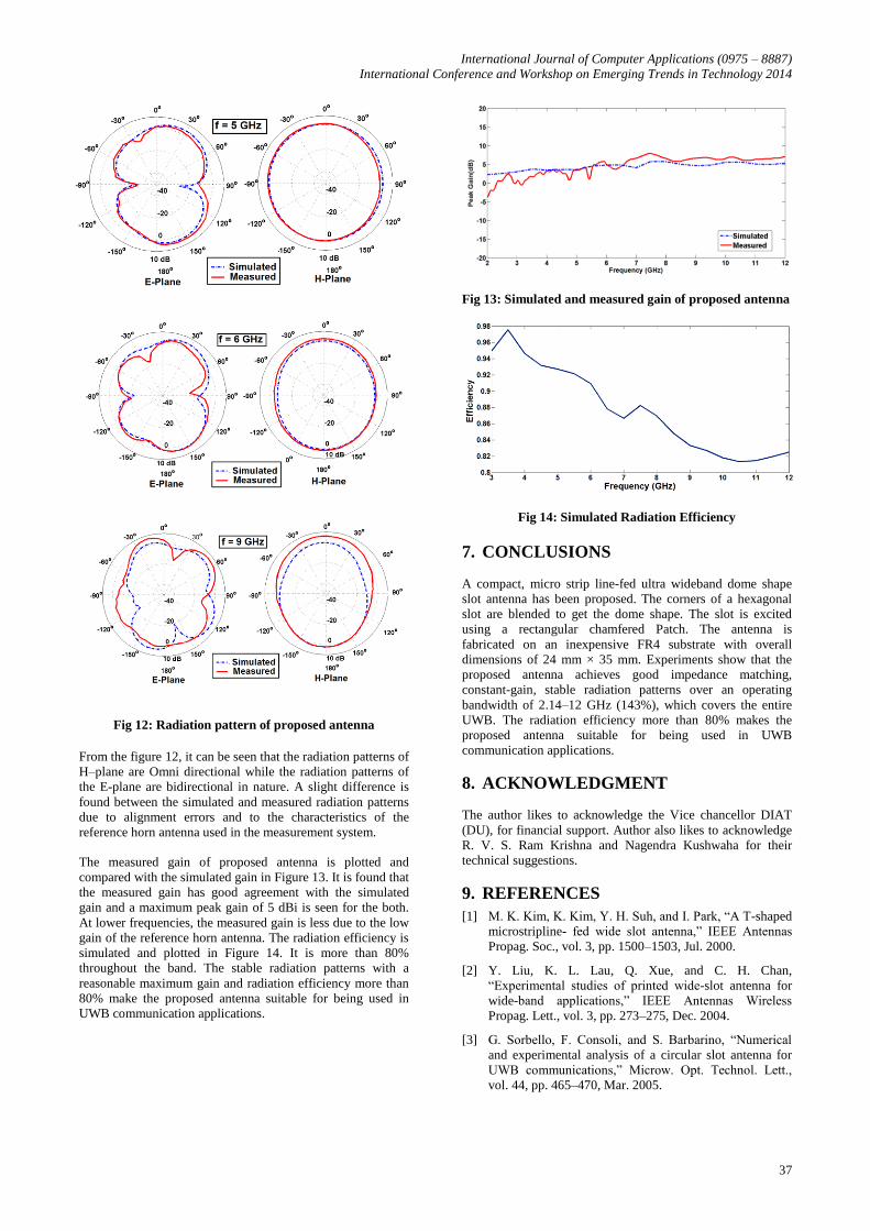
The measured gain of proposed antenna is plotted and
compared with the simulated gain in Figure 13. It is found that
the measured gain has good agreement with the simulated
gain and a maximum peak gain of 5 dBi is seen for the both.
At lower frequencies, the measured gain is less due to the low
gain of the reference horn antenna. The radiation efficiency is
simulated and plotted in Figure 14. It is more than 80%
throughout the band. The stable radiation patterns with a
reasonable maximum gain and radiation efficiency more than
80% make the proposed antenna suitable for being used in
UWB communication applications.
Fig 13: Simulated and measured gain of proposed antenna
Fig 14: Simulated Radiation Efficiency
7. CONCLUSIONS
A compact, micro strip line-fed ultra wideband dome shape
slot antenna has been proposed. The corners of a hexagonal
slot are blended to get the dome shape. The slot is excited
using a rectangular chamfered Patch. The antenna is
fabricated on an inexpensive FR4 substrate with overall
dimensions of 24 mm × 35 mm. Experiments show that the
proposed antenna achieves good impedance matching,
constant-gain, stable radiation patterns over an operating
bandwidth of 2.14–12 GHz (143%), which covers the entire
UWB. The radiation efficiency more than 80% makes the
proposed antenna suitable for being used in UWB
communication applications.
8. ACKNOWLEDGMENT
The author likes to acknowledge the Vice chancellor DIAT
(DU), for financial support. Author also likes to acknowledge
R. V. S. Ram Krishna and Nagendra Kushwaha for their
technical suggestions.
9. REFERENCES
[1] M. K. Kim, K. Kim, Y. H. Suh, and I. Park, “A T-shaped
microstripline- fed wide slot antenna,” IEEE Antennas
Propag. Soc., vol. 3, pp. 1500–1503, Jul. 2000.
[2] Y. Liu, K. L. Lau, Q. Xue, and C. H. Chan,
“Experimental studies of printed wide-slot antenna for
wide-band applications,” IEEE Antennas Wireless
Propag. Lett., vol. 3, pp. 273–275, Dec. 2004.
[3] G. Sorbello, F. Consoli, and S. Barbarino, “Numerical
and experimental analysis of a circular slot antenna for
UWB communications,” Microw. Opt. Technol. Lett.,
vol. 44, pp. 465–470, Mar. 2005.

International Journal of Computer Applications (0975 – 8887)
International Conference and Workshop on Emerging Trends in Technology 2014
38
[4] P. Li, J. Liang, and X. Chen, “Ultra-wideband elliptical
slot antenna fed by tapered microstrip line with U-shaped
tuning stub,” Microw. Opt. Technol. Lett., vol. 47, pp.
140–143, Oct. 2005.
[5] J. -Y. Sze and K. -L. Wong, “Bandwidth enhancement of
a microstripline- fed printed wide-slot antenna,” IEEE
Trans. Antennas Propag., vol. 49, pp. 1020–1024, Jul.
2001.
[6] X. Ding and A. F. Jacob, “CPW-fed slot antenna with
wide radiating apertures,” Inst. Elect. Eng. Proc. Microw.
Antennas Propagat., vol. 145, pp. 104–108, Feb. 1998.
[7] E. A. Soliman, S. Brebels, E. Beyne, and G. A. E.
Vandenbosch, “CPW-fed cusp antenna,” Microwave
Opt. Technol. Lett., vol. 22, pp. 288–290, Aug. 1999.
[8] M. Miao, B. L. Ooi, and P. S. Kooi, “Broadband CPW-
fed wide slot antenna,” Microwave Opt. Technol. Lett.,
vol. 25, pp. 206–211, May 5, 2000.
[9] U. Bhobe, C. L. Holloway, and M. Piket-May, “CPW fed
wide-band hybrid slot antenna,” in Proc. 2000 IEEE
Antennas Propagat. Soc. Int. Symp. Dig., pp. 636–639.
[10] Dastranj, A. Imani, and M. N. Moghaddasi, “Printed
wide-slot antenna for wideband applications,” IEEE
Trans. Antennas Propag., v 56, no. 10, pp. 3097–3102,
Oct. 2008.
[11] D. C. Chang, J. C. Liu, and M. Y. Liu, “Improved U-
shaped stub rectangular slot antenna with tuning pad for
UWB applications,” Electron. Lett., vol. 41, no. 20, pp.
1095–1097, 2005.
[12] J. Y. Sze and C. C. Chang, “Circularly polarized square
slot antenna with a pair of inverted-L grounded strips,”
IEEE Antennas Wireless Propag. Lett., vol. 7, pp. 149–
151, 2008.
[13] J. Y. Jan and J. C. Kao, “Novel printed wide-band
rhombus-like slot antenna with an offset microstrip-fed
line,” IEEE Antennas Wireless Propag. Lett. vol. 6, pp.
249–251, 2007.