design of combline filter for microwave p2p...
TRANSCRIPT

ii
DESIGN OF
COMBLINE FILTER
FOR MICROWAVE P2P LINK
By
ERKIN AHUNDOV
FINAL PROJECT REPORT
Submitted to the Department of Electrical & Electronic Engineering
in Partial Fulfillment of the Requirements
for the Degree
Bachelor of Engineering (Hons)
(Electrical & Electronic Engineering)
Universiti Teknologi PETRONAS
Bandar Seri Iskandar
31750 Tronoh
Perak Darul Ridzuan
Copyright 2012
by
Erkin Ahundov, 2012

iii
CERTIFICATION OF APPROVAL
DESIGN OF
COMBLINE FILTER
FOR MICROWAVE P2P LINK
by
Erkin Ahundov
A project dissertation submitted to the
Department of Electrical & Electronic Engineering
Universiti Teknologi PETRONAS
in partial fulfilment of the requirement for the
Bachelor of Engineering (Hons)
(Electrical & Electronic Engineering)
Approved:
__________________________
Dr. Wong Peng Wen
Project Supervisor
UNIVERSITI TEKNOLOGI PETRONAS
TRONOH, PERAK
September 2012

iv
CERTIFICATION OF ORIGINALITY
This is to certify that I am responsible for the work submitted in this project, that the
original work is my own except as specified in the references and acknowledgements,
and that the original work contained herein have not been undertaken or done by
unspecified sources or persons.
__________________________
Erkin Ahundov

v
ABSTRACT
Microwave filters are an essential part of communication systems operating in the
specified frequencies range. The main challenges faced by the designers today are
reduction of power loss and size of the filters. This paper is intended to develop a
cavity combline bandpass filter for microwave P2P link in order to introduce it to the
Malaysian market. The report attempts to find a suitable solution to the present
demand in the market by offering a new design used in the field. The methodology to
be used in the process of the project includes calculation of the filter parameters,
designing the filter in Ansys HFSS software, simulation, designing layout of the
transmission lines, fabrication, testing, and tuning. The paper also highlights the
history of the microwave engineering development, and reviews the previous studies
and projects of different groups to use as an example and reference in the current
case. The project is the Final Year Project of a Bachelor of Engineering (Hons)
Electrical & Electronics Engineering student at Universiti Teknologi PETRONAS.

vi
ACKNOWLEDGEMENTS
First of all, I would like to thank my supervisor Dr. Wong Peng Wen for guiding me
through the past two terms and sharing his knowledge and experience with me on the
matter. His support has been very helpful, so that the current project and the progress
that has been made would not be possible without him. Despite his other activities
and fully packed work schedule, Dr. Wong found and spent necessary time and effort
to assist me.
I would also like to thank my large family, especially parents, for the
continuous support of various forms throughout my whole life. Their motivation is
the main force that has been driving me through my university years and I owe all my
accomplishments to them.
I am also profoundly grateful to postgraduate students under Dr. Wong’s
supervision, Sohail Khalid and Sovuthy Cheab, for helping me with the current
project and guiding me through some difficulties I have encountered along the way.
In general, it has been a huge privilege and a great experience to study in and
be a part of Electrical & Electronics Engineering Department of Universiti Teknologi
PETRONAS for the past five years. And as my studies at the University are about to
be completed I would like to express my gratitude to all staff members of the
Department, both, academic and technical, for making these years here useful,
productive as well as pleasant.
Also, my appreciation goes to my friends and classmates here at Universiti
Teknologi PETRONAS for their help, time spent with me and, simply, friendship. My
university years would not be as fun and joyful without them and their company.

vii
TABLE OF CONTENTS
LIST OF TABLES ....................................................................................................... ix
LIST OF FIGURES ...................................................................................................... x
LIST OF ABBREVIATIONS ...................................................................................... xi
CHAPTER 1 PROJECT BACKGROUND .................................................................. 1
1.1 Introduction to Microwave Filters .................................................... 1
1.2 Problem Statement ........................................................................... 3
1.3 Objectives of the Project .................................................................. 4
1.4 The Scope of Study .......................................................................... 4
CHAPTER 2 LITERATURE REVIEW ....................................................................... 5
2.1 Two-Port Networks and ABCD parameters ..................................... 5
2.2 Two-Port Networks and the scattering matrix ................................. 8
2.3 Transverse Electromagnetic Mode of Wave Propagation .............. 10
2.4 Coaxial Transmission Lines ........................................................... 12
2.5 Microwave Combline Bandpass Filters ......................................... 14
CHAPTER 3 METHODOLOGY ............................................................................... 16
3.1 Process Flow Planning ................................................................... 16
3.2 Tools and Software Required ......................................................... 18
3.3 Gantt Chart and Key Milestones .................................................... 19

viii
CHAPTER 4 RESULTS AND DISCUSSION ........................................................... 20
4.1 MATLAB Simulation .................................................................... 20
4.2 Calculation of the Filter Parameters ............................................... 21
4.2.1 Constructing Lowpass Prototype ........................................... 21
4.2.2 Determining the Q-factor ....................................................... 22
4.2.3 Transforming to Combline Bandpass Filter .......................... 23
4.2.4 Physical Realisation of the Filter ........................................... 23
4.3 Design and Simulation in Ansys HFSS .......................................... 24
CHAPTER 5 CONCLUSIONS AND RECOMMENDATIONS ............................... 28
5.1 Conclusions .................................................................................... 28
5.2 Recommendations .......................................................................... 29
REFERENCES ............................................................................................................ 30
APPENDICES ............................................................................................................ 32
Appendix A MATLAB Simulation Coding ......................................... 33
Appendix B Lowpass to bandpass filter Transformation ..................... 34
Appendix C Calculation of the physical Dimensions .......................... 36
Appendix D Fiter Design in HFSS ....................................................... 40

ix
LIST OF TABLES
Table 1 The Bandpass combline filter specifications ................................................. 16
Table 2 Tools and Software required for the Project ................................................. 18

x
LIST OF FIGURES
Figure 1 Types of Filters and their sample frequency responses ................................. 1
Figure 2 Sample Responses of Chebyshev and Butterworth Lowpass Filters.............. 2
Figure 3 General Two-Port Network ........................................................................... 5
Figure 4 Two-port network terminated with load impedance ...................................... 6
Figure 5 Series Arm with impedance Z ........................................................................ 7
Figure 6 Shunt Arm with admittance Y ........................................................................ 7
Figure 7 Two-Port Network with [Z] impedance parameters ...................................... 8
Figure 8 TEM wave propagation in a parallel plate waveguide ............................... 10
Figure 9 TEM wave propagation in a coaxial transmission line ............................... 11
Figure 10 Coaxial Transmission Line ........................................................................ 12
Figure 11 Combline Filter .......................................................................................... 14
Figure 12 Combline Filter Equivalent Circuit ........................................................... 15
Figure 13 The project process flowchart.................................................................... 17
Figure 14 The frequency response of MATLAB simulation ....................................... 20
Figure 15 The Lowpass Prototype Filter.................................................................... 21
Figure 16 Filter Design in Ansys HFSS ..................................................................... 25
Figure 17 Initial Frequency Response in Ansys HFSS ............................................... 26
Figure 18 Frequency Response in Ansys HFSS (after optimization) ......................... 26
Figure 19 Static Capacitances of the Filter ............................................................... 36
Figure 20 Coupled Rectangular Bars between Parallel Plates ................................. 37
Figure 21 Coupling capacitances of rectangular bars .............................................. 39
Figure 22 Fringing capacitance of an isolated rectangular bar ................................ 39
Figure 23 Combline Filter Design in Ansys HFSS (various angles) ......................... 40

xi
LIST OF ABBREVIATIONS
P2P Peer-to-Peer
RF Radio Frequencies
TE Transverse Electric (Mode of wave propagation)
TM Transverse Magnetic (Mode of wave propagation)
TEM Transverse Electromagnetic (Mode of wave propagation)
HFSS High Frequency Structural Simulator
S-matrix Scattering Matrix (used to describe two-port networks)

1
CHAPTER 1
PROJECT BACKGROUND
1.1 Introduction to Microwave Filters
Today, microwave filters are used in a great variety of different fields, especially,
communication systems. The microwave filters, as the name suggests, operate on the
signals in the range of frequencies from 300 MHz to 300 GHz. With the spread of the
modern communication technologies over the last century, the demand and use of
different types of RF and microwave filters have dramatically increased.
Filters represent two-port networks that are designed to control the frequency
response of communication systems by allowing through the wanted signal
frequencies and rejecting the unwanted signal components. [1] In general, four types
of filters are used: lowpass, highpass, bandpass, and bandstop. The nearly ideal
sample frequency responses of the filters mentioned above are illustrated in Figure 1.
Figure 1 Types of Filters and their sample frequency responses

The frequencies denoted as
which are the boundary frequencies of the filters at which the system’s response will
decrease dramatically, thus, stopping the unwanted signal frequencies.
There are different types of filters depending on their frequency response
characteristics, such as, Butterworth, Chebyshev, Elliptic, and Bessel. Each of these
types has its own applications dependi
Due to the scope of the current project, a closer look would be taken on the
Chebyshev type filters only. The main characteristic of Chebyshev filters is that in
their frequency response the differences from the ideal
minimized in the cost of the ripples in th
frequency response of the Chebyshev low
much steeper than the one of the Butterworth filter, which is a great advantage in
most of filter applications. The gain in the undesired frequency range should be
minimized in order to prevent interference with other
presence of ripples in the passband is the trade
Figure 2 Sample Responses of Chebyshev and Butterworth Low
2
The frequencies denoted as fc on the graphs are called cut
which are the boundary frequencies of the filters at which the system’s response will
tically, thus, stopping the unwanted signal frequencies.
There are different types of filters depending on their frequency response
characteristics, such as, Butterworth, Chebyshev, Elliptic, and Bessel. Each of these
types has its own applications depending on the desired frequency response.
Due to the scope of the current project, a closer look would be taken on the
Chebyshev type filters only. The main characteristic of Chebyshev filters is that in
their frequency response the differences from the ideal filter characteristics are
minimized in the cost of the ripples in the passband. As shown on Figure
y response of the Chebyshev lowpass filter after the cut
much steeper than the one of the Butterworth filter, which is a great advantage in
most of filter applications. The gain in the undesired frequency range should be
minimized in order to prevent interference with other systems’ signals. However, the
presence of ripples in the passband is the trade-off of using Chebyshev filters.
Sample Responses of Chebyshev and Butterworth Lowp
on the graphs are called cut-off frequencies
which are the boundary frequencies of the filters at which the system’s response will
tically, thus, stopping the unwanted signal frequencies.
There are different types of filters depending on their frequency response
characteristics, such as, Butterworth, Chebyshev, Elliptic, and Bessel. Each of these
ng on the desired frequency response.
Due to the scope of the current project, a closer look would be taken on the
Chebyshev type filters only. The main characteristic of Chebyshev filters is that in
filter characteristics are
e passband. As shown on Figure 2, the
filter after the cut-off frequency is
much steeper than the one of the Butterworth filter, which is a great advantage in
most of filter applications. The gain in the undesired frequency range should be
systems’ signals. However, the
off of using Chebyshev filters. [2]
pass Filters
3
1.2 Problem Statement
Today, the communications is a very important field and it is very hard to imagine
our current environment with no electromagnetic waves in the atmosphere. Moreover,
the communication systems are still being developed and advanced bringing new
inventions and technologies every day.
In Malaysia, like in the rest of the world, the communication is a vastly
developing industry requiring more and more communication equipment. While the
demand grows, there is only a small number of companies that manufacture the
communication equipment. If we take a look at the production of microwave filters in
Malaysia, then we will find out that there are none.
Usually, the communication companies have to purchase the microwave
filters that have been produced and imported from other countries. Therefore, the aim
of this project is to develop a new design of the microwave combline bandpass filter
that would be demanded in local market and would cost less than analogous imported
products.
Then, if a closer look is taken at that transmission lines microwave filters, the
studies show that there are various types of filters produced that differ in the
transmission lines used and their layout (topology). The bandpass filters that are
mostly used today are interdigital filters because their frequency response is very
symmetrical and is a better choice for wide bandwidths. But when it comes to the
narrow bandwidths, the interdigital filters are quite large in size, which is a
disadvantage. Thus, the aim of the project is to design a combline microwave filter
that would be significantly smaller in size at the cost of less symmetric frequency
response. [13]

4
1.3 Objectives of the Project
The objectives that are aimed to be achieved upon the completion of this project are
as follows:
1. To study, understand the theory of the microwave filters, and develop the
skills in designing them.
2. To develop a high performance combline bandpass microwave filter that can
be implemented in the Malaysian market for a significantly lower price than
its imported analogies.
3. To test and then implement the filter in a real P2P link application.
1.4 The Scope of Study
While working on this project I have been focusing mainly on the research and
theoretical background on the subject. Literature review and study includes the
general theory of microwave engineering, types of microwave transmission lines
filters, comparison of their advantages and disadvantages, design steps and techniques
of the combline filters, fabrication, testing and tuning of the filter prototype.

5
CHAPTER 2
LITERATURE REVIEW
There have been a lot of research and studies done on the microwave signals and
filters theory, design, and applications. The demand in the market and these extensive
studies led to the industry’s rapid development throughout the twentieth century.
2.1 Two-Port Networks and ABCD parameters
Two-port network is a mathematical model that is used to represent portions of larger
electric circuits as a whole block with parameters that would characterize its response
to a given input. A general representation of two-port network is shown in Figure 3
below, where V1 and I1 are input voltage and current, respectively, and V2 and I2 are
the output voltage and current, respectively. [3]
Figure 3 General Two-Port Network
A two-port network can be easily characterized by the ABCD parameters,
which are found in the following way [3]
=
2
2
1
1
I
V
DC
BA
I
V
(2.1.1)
where [ ]TDC
BA=
is called the Transfer Matrix.

6
The use of ABCD matrix to define the characteristics of a two-port network is
the most commonly used technique. The network parameters are found using the
following formulas [3]
02
1
2=
=I
V
VA
02
1
2 =
=V
I
VB
02
1
2 =
=I
V
IC
02
1
2 =
=V
I
ID
If a two-port network is terminated with load impedance, ZL, as shown on
Figure 4, the input impedance is calculated as follows:
1
1
I
VZ in =
Using the relationship between the input and output of a two-port network
described in equation (2.1.1) we have the following [3]
22
22
1
1
DICV
BIAV
I
V
++
=
DICV
BIAV
++
=22
22 /
DCZ
BAZZ
L
Lin +
+=
Figure 4 Two-port network terminated with load impedance
7
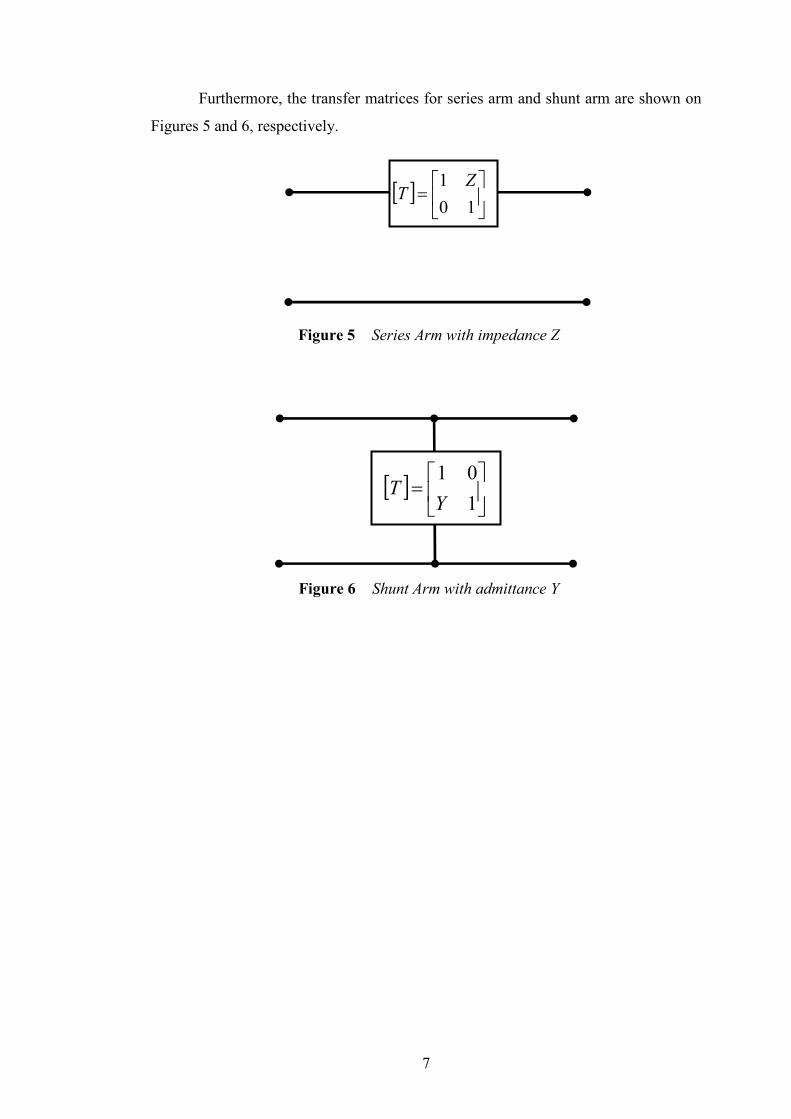
Furthermore, the transfer matrices for series arm and shunt arm are shown on
Figures 5 and 6, respectively.
Figure 5 Series Arm with impedance Z
Figure 6 Shunt Arm with admittance Y
[ ]
=
1
01
YT
[ ]
=
10
1 ZT

8
2.2 Two-Port Networks and the scattering matrix
Another set of parameters is also widely used in characterizing and analyzing two-
port networks, called the scattering matrix or also S parameters. Figure 7 shows a
typical two-port network illustrating all the voltage and current parameters at the
input and output.
Figure 7 Two-Port Network with [Z] impedance parameters
Thus, we can represent the voltage in terms of the current and impedance
matrices [3]
]][[][ IZV =
where
=
2
1][
V
VV
=
2
1][
I
II
=
2221
1211][
ZZ
ZZZ
Now let
][][][2
1IV
a
aa +=
= and ][][][
2
1IV
b
bb −=
=
Then also let
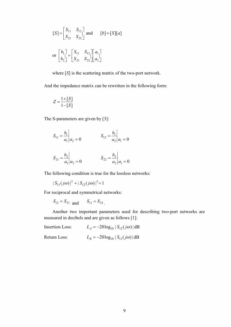
9
=
2221
1211][
SS
SSS and ]][[][ aSb =
or
=
2
1
2221
1211
2
1
a
a
SS
SS
b
b
where [S] is the scattering matrix of the two-port network.
And the impedance matrix can be rewritten in the following form:
][1
][1
S
SZ
−+
=
The S-parameters are given by [3]:
021
111 ==
aa
bS
012
112 ==
aa
bS
021
221 ==
aa
bS
012
222 ==
aa
bS
The following condition is true for the lossless networks:
1|)(||)(| 212
211 =+ ωω jSjS
For reciprocal and symmetrical networks:
2112 SS = and 2211 SS = .
Another two important parameters used for describing two-port networks are
measured in decibels and are given as follows [1]:
Insertion Loss: |)(|log20 1210 ωjSLA −= dB
Return Loss: |)(|log20 1110 ωjSLR −= dB

10
2.3 Transverse Electromagnetic Mode of Wave Propagation
There are different types of electromagnetic wave propagation used in transmission
lines, such as transverse electric (TE), transverse magnetic (TM), and transverse
electromagnetic (TEM).
Transverse electromagnetic, in particular, is the mode of wave propagation
when the electric and magnetic field lines are both perpendicular to the direction of
wave travel through the media. TEM mode can only exist when there are two or more
conductors, and when the cross-sectional dimensions of the transmission lines are
relatively smaller than the signal wavelength. [4]
Figure 8 shows an example of TEM mode of propagation through a parallel
plate waveguide. As seen on the figure, the magnetic field lines are circular around
the conductors, whilst electric field lines are between these conductors, and both of
them are in the planes perpendicular to the direction of wave travel.
Figure 8 TEM wave propagation in a parallel plate waveguide [4]
TEM mode of propagation is very useful, because the cutoff frequency in it is
equal to zero, i.e. fc=0. Other advantages of this wave propagation mode are that there
is no dispersion, or in other words, the various frequencies present in a signal would
travel at the same speed.
Another type of transmission lines that is suitable for TEM mode of
propagation is coaxial cable. As seen on the Figure 9, the electric field lines are

11
radial, whereas the magnetic field lines are circular, and both of them are in the cross
sectional plane of the cable, which is transverse to the direction of wave travel along
the coaxial transmission line.
Figure 9 TEM wave propagation in a coaxial transmission line [4]

12
2.4 Coaxial Transmission Lines
Coaxial transmission lines consist of a wire conductor surrounded by a cylindrical
conducting shield. The two conductors (inner and outer) are divided by a tubular
dielectric insulator between them, as shown in Figure 10. In microwave
communications, coaxial transmission lines mainly support the TEM mode of wave
propagation which is a great advantage of using them. [5]
Figure 10 Coaxial Transmission Line
If we direct the z-axis along the transmission line, i.e. along the wave
propagation, then according to TEM mode’s conditions: 0=zE and 0=zB .
The characteristic impedance of a lossless coaxial transmission line is calculated
the following way: [2]
C
LZ =0 (2.4.1)
The phase velocity of the TEM wave propagation inside transmission line is:
εµ0
11==
LCvp
(2.4.2)
And the propagation constant is found by:
))(( CjGLjR ωωγ ++= (2.4.3)

13
where L = inductance per unit length,
R = resistance per unit length,
C = capacitance per unit length,
G = conductance per unit length,
µ0 = permeability of a vacuum,
ε = material permittivity.
The characteristic impedance can be furthermore elaborated by combining the
equations (2.4.1) and (2.4.2):
a
bZ
r
ln60
0εΩ
= [5]
where εr is the relative permittivity of dielectric material, a and b are the radii of
the inner and outer conductors, respectively.
Both, electric and magnetic, fields are changed with the relation to the radius
from the center of the inner conductor (vary with 1/r) and are given by the following
formulas:
)/ln( abr
VEr =
022 rZ
V
r
IH
ππφ ==

14
2.5 Microwave Combline Bandpass Filters
Microwave Combline filters are used in many communications applications for a very
wide range of frequencies. Their main advantage is that they are compact in size and
light in weight. Also, the combline filters are very stable to the changes in
temperature and are very suitable for extreme operating conditions. [6]
Figure 11 Combline Filter [7]
It is seen on Figure 11, that a combline filter consists of several transmission
lines that are all short-circuited at one end. The other ends of the lines are connected
to ground through lumped capacitors.
The combline filter operates in the following way. First, if we imagine that the
lumped capacitors were taken out; the resonance frequency of the lines would be
equal to the quarter wave. But at the same time, the couplings are supposed to
resonate at the same frequency, resulting in all-stop filter. Now, if we introduce the
capacitors, the lines would start resonating together along with capacitors at
frequency which is lower than the quarter wave frequency. [6] [7] [8]
Compared to interdigital filters the combline filters are much smaller in size
due to decreased length of transmission lines, as well as decreased spacing between
the lines.
In order to better understand and predict the performance of combline filters, a
simplified equivalent circuit is developed, illustrated on Figure 12.

Figure 12
Also, some formulas have been derived in order to calculate the filter’s
physical parameters, listed below [6]:
θωCYrr = tan( 00
tan(
=
rr
Lrr
Y
Cn
θα
1,1,
tan(
+
++ =
rr
rrrr
nn
KY
,1− −−= rrrrr YYY
12111 YYYY N −==
11
10n
YY N −== +
1
1,01n
YY NN == +
where Yr are
Yrr are the coupling admittances between
θ0 is the electrical length at the center frequency.
15
Figure 12 Combline Filter Equivalent Circuit
Also, some formulas have been derived in order to calculate the filter’s
parameters, listed below [6]:
βC
=)
2/1
0 )
θ
(r=1,…, N)
1
0 )tan(
+
θ (r=1,…, N-1)
1, +− rrY (r=2,…, N-1)
)0121
12cos(
11
θnnY −+ (r=1 and N)
)cos(
1
01 θ
)cos(
1
01 θ
admittances of the resonators,
are the coupling admittances between neighboring
is the electrical length at the center frequency.
ombline Filter Equivalent Circuit
Also, some formulas have been derived in order to calculate the filter’s
(2.5.1)
(2.5.2)
(2.5.3)
(2.5.4)
(2.5.5)
(2.5.6)
(2.5.7)
neighboring resonators,

16
CHAPTER 3
METHODOLOGY
The parameters of the bandpass combline filter that is yet to be designed are listed
below:
Table 1 The Bandpass combline filter specifications
Parameter Specification
Frequency Range 824 MHz – 849 MHz
Center Frequency, f0 836.5 MHz
Bandwidth (BW), ∆f 25 MHz
Insertion Loss (Max), LA 1.0 dB max (passband)
Return Loss (Min), LR 20 dB min (passband)
Attenuation 60 dB @ 800 MHz
@ 869 MHz
Impedance, Z 50 Ohm nominal
3.1 Process Flow Planning
After the problem has been defined and the objectives have been clearly stated, the
literature review was performed in order to get the general and then specific
knowledge in microwave engineering and study the previous projects that have been
done in the field. The literature based research is very important for the project as it
forms the basis for the successful and meaningful outcome.
The thorough study during the research allowed me to sketch a plan of work
to be done to reach the objectives. Detailed planning was important to be written up
defining the activities and strict timeframes within which the important milestones
have to be reached. The process flowchart for the current project is illustrated in

17
Figure 13 below which highlights all main steps that lead to the project’s successful
completion.
Figure 13 The project process flowchart
After the methodology was defined, calculation of the filter physical
parameters started. It included computation of the filter’s admittances, the values of
the capacitors and derivation of its transfer function. Afterwards the dimensions of
the transmission lines (resonators) were computed as well as the spacing between the
resonators.
When the filter parameters had been acquired, the filter simulation was started
using the Ansys HFSS 3D simulation software. It includes building the system in the
software’s interface, then simulating it and acquisition of the filter’s frequency
response. Based on the simulation results, optimization of the resonators’ dimensions
was required in order to correct the inaccuracies of the calculations.
After the filter parameters are confirmed and its simulated frequency response
satisfies the objectives, the circuit from the Ansys HFSS would be extracted to the
Computer-Aided Design (CAD) computer software. Afterwards, the extracted CAD
design would be used for the filter fabrication that is to be done in the labs of
Universiti Teknologi Petronas.
Problem Statement
& Topic selection
Literature Review,
Process Flow
Planning &
Methodology
Calculation of the
Filter Parameters,
and Transmission
Lines Dimensions
Building the Filter
Circuit on HFSS
Software and
Simulation
Optimization of the
Transmission Lines
Parameters (HFSS)
Extracting the
Circuit Layout using
CAD software
Filter Prototype
Fabrication
Testing and Fine-
Tuning of the
Prototype
Obtaining Results &
Project Defense

18
The fabricated prototype then needs to be tested using the frequency analyzer
device, which will allow us to plot the frequency response of the filter. Based on the
obtained results, fine tuning of the filter prototype may be required.
3.2 Tools and Software Required
Table 2 Tools and Software required for the Project
Tools / Software Function
MATLAB • to simulate the Chebyshev Type 1 filter
• to calculate the filter parameters
Ansys HFSS • to build the 3D model of the filter and obtain simulated
frequency response
• to optimize the filter parameters, if required
CAD Software • to extract the model layout for fabrication
Cavity Fabricator • to fabricate the filter prototype
Frequency Analyzer • to test the filter prototype and obtain its frequency
response

19
3.3 Gantt Chart and Key Milestones
Final Year Project I (May 2012)
Final Year Project II (September 2012)
Week
N
o Task Name 1 2 3 4 5 6 7
8 9 10 11 12 13 14
1 Topic Selection
M
I
D
S
E
M
B
R
E
A
K
2 FYP Briefing
3 Literature Review
4 Submission of Extended
Proposal
5 Meeting with FYP supervisor /
FYP Sharing Session
6 Proposal Defense
7 Simulation in MATLAB.
Calculation of Parameters
8 Submission of Interim Draft
Report
9 Submission of Interim Report
Week
No Task Name 1 2 3 4 5 6 7
8 9 10 11 12 13 14 15
1 Calculation of Filter
Parameters
M
I
D
S
E
M
B
R
E
A
K
2 Building model in Ansys
HFSS & Optimization
3 Extraction via CAD and
Prototype Fabrication
4 Testing and Fine-Tuning the
Prototype
5 Progress Report Submission
6 ElectrEX (Pre-EDX)
7 Submission of Draft Report
8 Submission of Dissertation
(Soft Bound)
9 Submission of Technical
Paper
10 Oral Presentation
11 Submission of Project
Dissertation (Hard Bound)
Process
Milestone

20
CHAPTER 4
RESULTS AND DISCUSSION
4.1 MATLAB Simulation
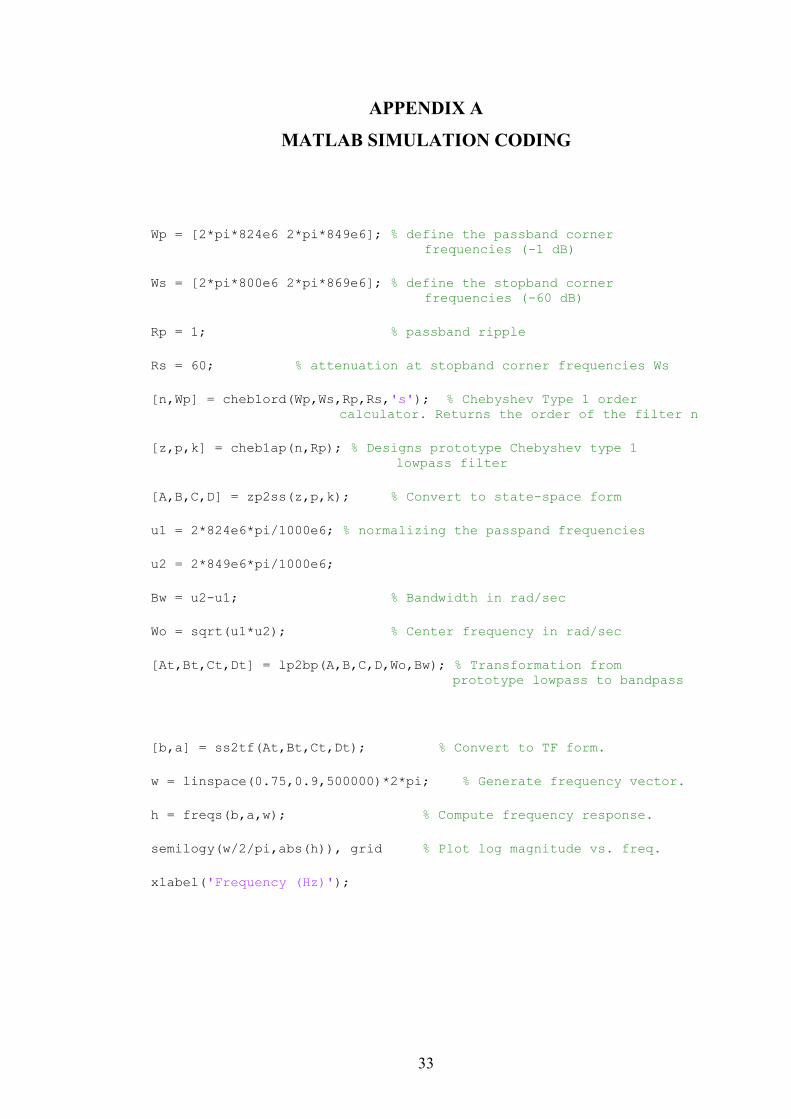
In order to get a general idea of filter’s frequency response, a filter is simulated in
MATLAB. First, the order of the Chebyshev filter is calculated by the cheb1ord
command setting the passband ripples to be within 1 dB. Then Chebyshev Type 1
lowpass filter prototype is generated using the cheb1ap command with the unity
cutoff frequency and the order is returned by the previous MATLAB function. The
lowpass prototype is then transformed into a bandpass filter that meets the
requirements of this project by the aid of the lp2bp function. The coding that was
used in MATLAB is listed in Appendix A.
After running the program the frequency response graph shown on Figure 14
was obtained from the filter simulation. The function cheb1ord returned the value
n for the order of the system to be 6. Therefore, the filter designed and simulated in
MATLAB is 6th order Chebyshev Type 1.
Figure 14 The frequency response of MATLAB simulation

4.2 Calculation of the Filter Parameters
There are several stages of mathematical analysis that lead to finding the filter’s
physical parameters or dimensions. First, a lowpass prototype filter is constructed
based on the selectivity criteria and is then transformed into a bandpass filter with a
specific center frequency and bandwidth.
4.2.1 Constructing Lowpass Prototype
The lowpass prototype filter is a
angular frequency consisting of lumped circuit elements and
nominal impedance. [
However, first of all, the order of the filter to be designed needs to be calculated
using the following formula:
[log20 10
≥L
N A
where LA = 60 dB is the stopband insertion loss
loss; and
2.
The right side of the expression above yields 5.92, thus, the order of the filter to
be designed is N=6, which confirms the output of the MATLAB function.
order Chebyshev lowpass prototype netw
shunt capacitors and impedance inverters.
Next, the ripple factor is computed:
10( 10/ −= RLε
21
Calculation of the Filter Parameters
There are several stages of mathematical analysis that lead to finding the filter’s
physical parameters or dimensions. First, a lowpass prototype filter is constructed
based on the selectivity criteria and is then transformed into a bandpass filter with a
specific center frequency and bandwidth.
Constructing Lowpass Prototype
The lowpass prototype filter is a lossless two-port network with the unity cut
consisting of lumped circuit elements and is operated at 1 Ohm
[9]
However, first of all, the order of the filter to be designed needs to be calculated
using the following formula:
])1([
62/12 −+
++
SS
LR
[6]
60 dB is the stopband insertion loss; LR = 20 dB is the passband return
.76 is the ratio of the stopband to passband frequencies.
The right side of the expression above yields 5.92, thus, the order of the filter to
, which confirms the output of the MATLAB function.
order Chebyshev lowpass prototype network is illustrated in Figure 1
shunt capacitors and impedance inverters.
Figure 15 The Lowpass Prototype Filter
Next, the ripple factor is computed:
1005.0)1 2/1 =− [6]
There are several stages of mathematical analysis that lead to finding the filter’s
physical parameters or dimensions. First, a lowpass prototype filter is constructed
based on the selectivity criteria and is then transformed into a bandpass filter with a
with the unity cut-off
is operated at 1 Ohm
However, first of all, the order of the filter to be designed needs to be calculated
20 dB is the passband return
is the ratio of the stopband to passband frequencies.
The right side of the expression above yields 5.92, thus, the order of the filter to
, which confirms the output of the MATLAB function. The 6th
ork is illustrated in Figure 15. It consists of
22
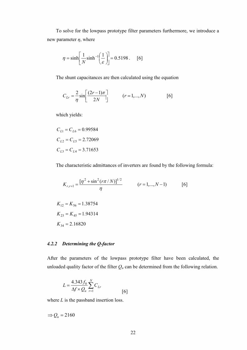
To solve for the lowpass prototype filter parameters furthermore, we introduce a
new parameter η, where
5198.01
sinh1
sinh 1 =
= −
εη
N. [6]
The shunt capacitances are then calculated using the equation
−=
N
rCLr
2
)12(sin
2 πη
),...,1( Nr = [6]
which yields:
71653.3
72069.2
99584.0
43
52
61
==
==
==
LL
LL
LL
CC
CC
CC
The characteristic admittances of inverters are found by the following formula:
ηπη 2/122
1,
)]/(sin[ NrK rr
+=+ )1,...,1( −= Nr [6]
16820.2
94314.1
38754.1
34
4523
5612
=
==
==
K
KK
KK
4.2.2 Determining the Q-factor
After the parameters of the lowpass prototype filter have been calculated, the
unloaded quality factor of the filter Qu can be determined from the following relation.
∑=×∆
=N
r
Lr
u
CQf
fL
1
0343.4
[6]
where L is the passband insertion loss.
2160=⇒ uQ
23
4.2.3 Transforming to Combline Bandpass Filter
Based on the parameters of the lowpass prototype we are now able to compute the
parameters of the combline bandpass cavity filter. In order to make the filter more
compact we choose the electrical length of the resonators at the center frequency to be
θ0=45o or π/4 radians. It means that the actual resonators will be 1/8 of the
wavelength long. [6] [7] [10]
The steps taken to calculate the admittances of the transmission lines are
shown in Appendix B and after scaling them to 50 Ohm, the impedances of the
resonators and couplings between them are as follows:
pFC
Z
ZZ
ZZ
ZZ
ZZ
ZZ
ZZ
ZZ
805.3
147.2231
379.2130
163.1544
005.180
404.52
958.52
641.68
230.69
34
4523
5612
6701
43
52
61
70
=
Ω=
Ω==
Ω==
Ω==
Ω==
Ω==
Ω==
Ω==
4.2.4 Physical Realisation of the Filter
The combline filter to be constructed will consist of rectangular aluminium bars
that are shorted at one end and are connected to ground through a capacitor at the
other. The bars are located in the middle between ground planes that act like the outer
conductor of the coaxial line, while the bars being the inner ones. [11] [12]
The steps in calculating the physical dimensions of the resonators are all shown
in Appendix C. The depth of the filter is b=15 mm, while the thickness of each
resonator is t = 3 mm. Listed below are the widths of the resonators and the spacing
between them [14]:
24
mmww
mmww
mmww
mmww
44.14
46.14
10.12
18.11
43
52
61
70
==
==
==
==
mmS
mmSS
mmSS
mmSS
6.12
45.12
95.10
25.2
34
4523
5612
6701
=
==
==
==
The length of the resonators is equal to one-eighth of the wavelength at the center
frequency and is calculated below:
mmf
cL
o
o
83.44360
45
0
=×=
The capacitance at the end of each resonator is realised by attached conductor
plates which are spaced from the ground plane by a distance d. From the definition of
capacitance:
d
AC r 0εε=
[5]
Choosing the dimensions of the plates to be 12 mm × 18 mm × 0.5 mm the
spacing between the capacitor plate and the ground (the side wall of the filter) is
determined to be d = 0.50 mm.
4.3 Design and Simulation in Ansys HFSS
The filter design was built using the Ansys HFSS (High Frequency Structural
Simulator) software. The coaxial resonators were realised by the coupled aluminium
rectangular bars between parallel ground planes that act as the outer conductors. The
TEM lines 0 and 7 are not resonators though they are λ/8 long, but are the part of the
impedance transformation circuit.

25
The filter was built in symmetry relatively to the X and Z axes, so it would be
much easier to alter the spacing between the resonators using variables while keeping
the symmetry of the circuit.
The resonators (lines 1 to 6) have attached thin conductor plates with an equal
area at one end which act as the capacitors and are distanced from the side wall of the
filter (electrical ground) to produce the desired lumped capacitance that has been
calculated for the combline filter.
The filter design constructed in Ansys HFSS is shown in Figure 16 and its views
from various angles are presented in Appendix D.
Figure 16 Filter Design in Ansys HFSS
The illustrated structure was analysed in Ansys HFSS and the initially obtained
frequency response of the scattering parameters is plotted and shown in Figure 17. As
seen from the plot, the center frequency of the filter is shifted by 90 MHz, i.e. is at
746 MHz. Moreover, the loss in the passband is very high and reaches -6 dB.

26
Figure 17 Initial Frequency Response in Ansys HFSS
The flaws mentioned above can be eliminated by optimizing the structure. The
optimization in Ansys HFSS involves alteration of certain parameters until the aim is
reached. Our goal is to make the passband return loss be in the range below -20 dB
and the roll-off to 60 dB attenuation to be reached at 800 and 869 MHz. The variable
parameters used in the optimization are the resonators’ widths, spacing between the
resonators, and the spacing between the capacitance plates and the ground. The
frequency response of the filter after the optimization is illustrated on Figure 18.
Figure 18 Frequency Response in Ansys HFSS (after optimization)

27
By altering the spacing between the capacitor plates and the ground, i.e. by
varying the capacitance, the desired center frequency has been reached. Moreover,
after optimizing the spacing between resonators the loss in the passband has been
minimized to be within -2 dB range, and the lowest value of return loss is about -6 dB
which is far less from the required -20 dB margin.
Due to the time and resources constraints that this project is faced with, the
fabrication of the filter does not seem possible at the moment. However, even prior to
that, a further optimization of the filter parameter is due to performed in order to
obtain a better frequency response, namely to minimize the passband ripples and
decrease the passband return loss below the -20 dB margin.

28
CHAPTER 5
CONCLUSIONS AND RECOMMENDATIONS
5.1 Conclusions
Since the project has started in the beginning of the previous term, I have acquired a
lot of useful knowledge and skills in microwave engineering, which is one of the
most important and widely used in communication systems and technologies
nowadays. Communications, in turn, have undertaken a rapid development
throughout the twentieth century and have become an essential part of our lives.
By working on this project and doing an extensive research on the subject, I
have gained a valuable knowledge about the microwave filters, various methods of
their design and fabrication. There are a lot of design techniques based on the type of
transmission lines used and their layout topology, all of them have their advantages
and drawbacks, so, it is up to the designer to decide which filter characteristic is the
most important in the cost of the others.
Thus, it was decided to use the coaxial transmission lines as the resonators for
our combline bandpass filter because the wave propagation mode in them is always
Transverse Electromagnetic (TEM) which is very useful in such high frequencies.
Another advantage of coaxial transmission lines filter is that the quality factor that
can be achieved using the rectangular bars is quite high, resulting in high selectivity
of the filter.
Therefore, one can conclude, that it is obviously feasible to achieve the
objectives predefined in the beginning of the project progress. Moreover, it seems
very realistic to develop a high performance microwave filter that can be
implemented in the Malaysian market for a significantly lower price than its imported
analogies.

29
Unfortunately, due to time and other resources constraints the current project
may not seem to have be successfully completed. However, important lessons have
been learnt and very useful and practical skills have been developed as well as new
ones are acquired.
5.2 Recommendations
As for the future projects and studies in the same field, there is still a plenty of work
to be done in order to complete the predefined objectives and get a better idea and full
picture of the filter fabrication, testing and implementation. An essential part of the
project is ought to be completed, which includes fine optimization of the filter
parameters, fabrication, testing, and fine-tuning.
The step to be completed at this point of time is the optimization of the structure
parameters. It includes altering the widths of the resonators, spacing between them,
and distance between the capacitor plates and the ground until the desired frequency
response is obtained.
Even if an ideal frequency response is obtained after the optimization using the
software, most probably, the frequency response of the fabricated filter would differ
from it. Therefore, fine tuning of the filter should be performed by inserting and
tightening the screws inside the filter box. By changing the screws’ penetration, we
are able vary the couplings between resonators and the lumped capacitances attached
to them; thus, alter the frequency response characteristics if there are any
inaccuracies.

30
REFERENCES
[1] Cameron, R. J., Kudsia, C. M., Mansour, R. R. (2007). Microwave Filters for
Communication Systems. Fundamentals, Design, and Applications. Hoboken,
NJ: John Wiley & Sons, Inc.
[2] Pozar, D. M. (1997). Microwave Engineering. Wiley
[3] Nilsson, J. W., Riedel, S. A. (2008). Electric Circuits (8th ed.). Prentice Hall.
[4] Transverse Electromagnetic Mode. (2010). Microwave Encyclopedia. Retrieved
July 11, 2012, from http://www.microwaves101.com/encyclopedia/TEM.cfm
[5] Chi Shen, L., Au Kong, J. (1987). Applied Electromagnetism. PWS
Engineering.
[6] Hunter, I. C. (2001). Electromagnetic Waves Series 48: Theory and Design of
Microwave Filters. IET.
[7] Matthaei, G. L., Young, L., and Jones, E. M. T. (1964). Microwave Filters,
Impedance-Matching Networks and Coupling Structures. New York: McGraw-
Hill.
[8] Matthaei, G. L. (1963). Combline Bandpass filters of narrow or moderate
bandwidth. The Microwave Journal.
[9] Schaumann, R., Van Valkenburg, M. E. (2001). Design of Analog Filters,
Oxford University Press.
[10] Puglia, K. (2000). A general design procedure for bandpass filters derived from
lowpass prototype elements: Part I. The Microwave Journal, 43, 22–38.

31
[11] Young, L., Matthaei, G. L. (1962). Microwave Filters and Coupling Structures.
Quarterly Progress Report 4, SRI Project 3527, Contract DA 36-039
SC87398, Stanford research Institute, California.
[12] Che Wang, Zaki, K. A., Atia, A. E., Dolan, T. G. (1998). Dielectric combline
resonators and filters. Microwave Theory and Techniques, IEEE Transactions,
46(12), Part 2, 2501-2506.
[13] Mansour, R. R. (2004). Filter technologies for wireless base stations.
Microwave Magazine, IEEE 5(1), 68 – 74.
[14] Getsinger, W. J. (1962). Coupled Rectangular Bars Between Parallel Plates.
IEEE Transactions on Microwave Theory and techniques, 10(1), 65-72.

32
APPENDICES
33
APPENDIX A
MATLAB SIMULATION CODING
Wp = [2*pi*824e6 2*pi*849e6]; % define the passband corner
frequencies (-1 dB)
Ws = [2*pi*800e6 2*pi*869e6]; % define the stopband corner
frequencies (-60 dB)
Rp = 1; % passband ripple
Rs = 60; % attenuation at stopband corner frequencies Ws
[n,Wp] = cheb1ord(Wp,Ws,Rp,Rs,'s'); % Chebyshev Type 1 order
calculator. Returns the order of the filter n
[z,p,k] = cheb1ap(n,Rp); % Designs prototype Chebyshev type 1
lowpass filter
[A,B,C,D] = zp2ss(z,p,k); % Convert to state-space form
u1 = 2*824e6*pi/1000e6; % normalizing the passpand frequencies
u2 = 2*849e6*pi/1000e6;
Bw = u2-u1; % Bandwidth in rad/sec
Wo = sqrt(u1*u2); % Center frequency in rad/sec
[At,Bt,Ct,Dt] = lp2bp(A,B,C,D,Wo,Bw); % Transformation from
prototype lowpass to bandpass
[b,a] = ss2tf(At,Bt,Ct,Dt); % Convert to TF form.
w = linspace(0.75,0.9,500000)*2*pi; % Generate frequency vector.
h = freqs(b,a,w); % Compute frequency response.
semilogy(w/2/pi,abs(h)), grid % Plot log magnitude vs. freq.
xlabel('Frequency (Hz)');

34
APPENDIX B
LOWPASS TO BANDPASS FILTER TRANSFORMATION
The lowpass prototype values are as follows:
71653.3
72069.2
99584.0
43
52
61
==
==
==
LL
LL
LL
CC
CC
CC
16820.2
94314.1
38754.1
34
4523
5612
=
==
==
K
KK
KK
An intermediate parameter α is calculated [6]:
0308.26)](tan1[)tan(
)tan(2
02
00
00 =++∆
=θθθω
θωα
From the formula (2.5.1)
10
00
1090263.1)tan(
1 −×==θω
β
Also from (2.5.1)
βC
Yrr =
Choosing Yrr = 1, we can determine the value of the lumped capacitance at the
end of each resonator
101090263.1 −×== βC

35
Based on (2.5.2) another set of intermediate parameters nr is computed that will
be later used for determining the couplings between resonators
8359.9
4156.8
0914.5
43
52
61
==
==
==
nn
nn
nn
The couplings between the resonators are calculated using (2.5.7) and (2.5.3)
02241.0
02347.0
03238.0
27777.0
34
4523
5612
6701
=
==
==
==
Y
YY
YY
YY
The admittances of the transmission lines are then calculated using the formulas
(2.5.4) to (2.5.6)
95412.0
94415.0
72843.0
72223.0
43
52
61
70
==
==
==
==
YY
YY
YY
YY
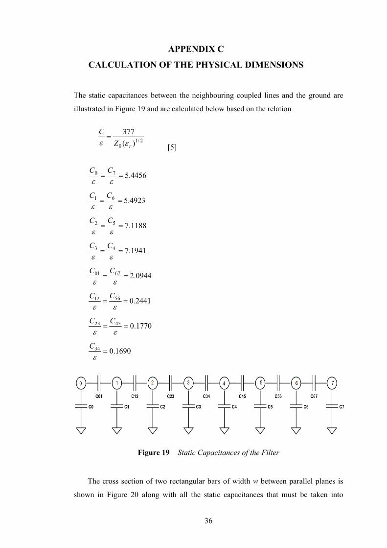
CALCULATION OF THE P
The static capacitances between the neighbouring coupled lines and the ground are
illustrated in Figure 19
/10 )(
377
rZ
C
εε=
1690.0
1770.0
2441.0
0944.2
1941.7
1188.7
4923.5
4456.5
34
4523
5612
6701
43
52
61
70
=
==
==
==
==
==
==
==
ε
εε
εε
εε
εε
εε
εε
εε
C
CC
CC
CC
CC
CC
CC
CC
Figure 19
The cross section of two rectangular bars of width
shown in Figure 20
36
APPENDIX C
CALCULATION OF THE PHYSICAL DIMENSIONS
The static capacitances between the neighbouring coupled lines and the ground are
19 and are calculated below based on the relation
2
[5]
1770
2441
0944
1941
1188
4923
4456
Figure 19 Static Capacitances of the Filter
The cross section of two rectangular bars of width w between paral
along with all the static capacitances that must be taken into
HYSICAL DIMENSIONS
The static capacitances between the neighbouring coupled lines and the ground are
calculated below based on the relation
between parallel planes is
along with all the static capacitances that must be taken into
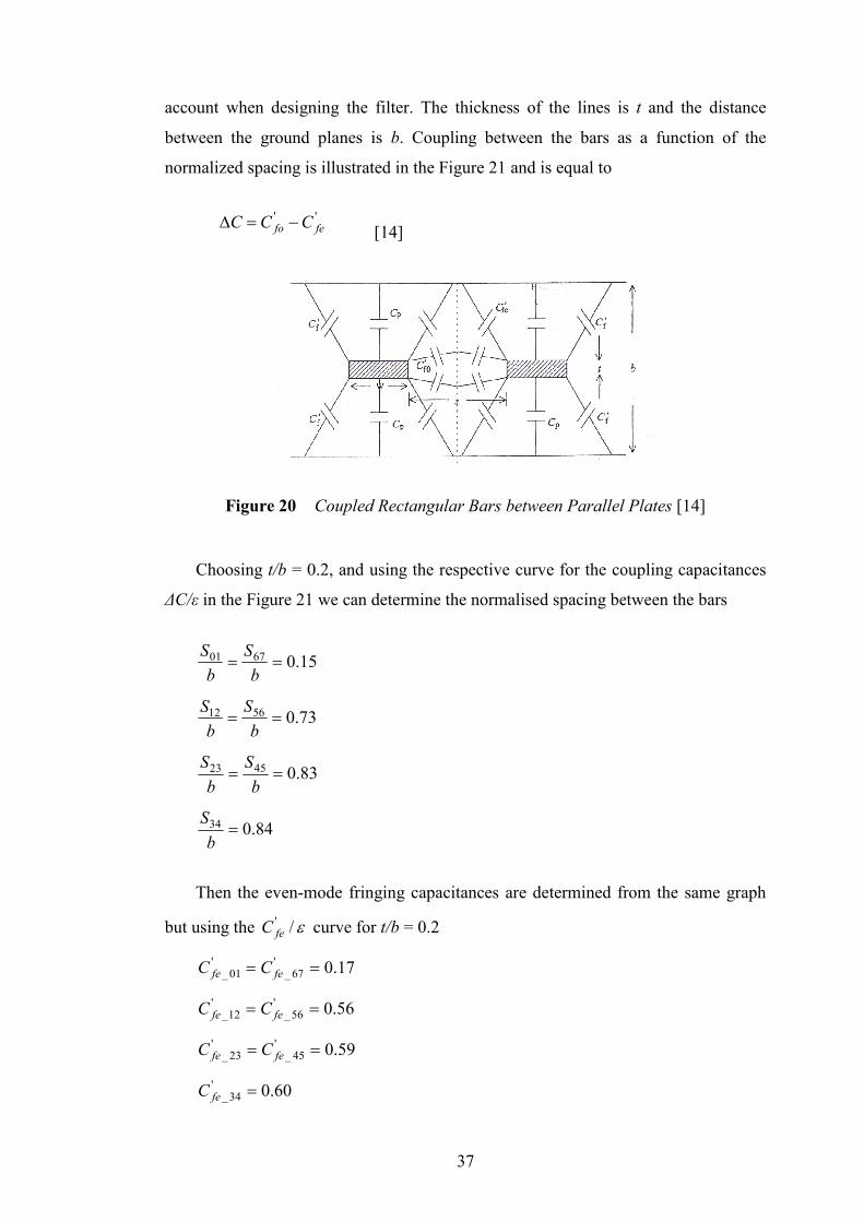
account when designing the filter. The thickness of the lines is
between the ground planes is
normalized spacing is illustr
'fo CCC −=∆
Figure 20
Choosing t/b = 0.2,
∆C/ε in the Figure 21
84.0
83.0
73.0
15.0
34
4523
5612
6701
=
==
==
==
b
S
b
S
b
S
b
S
b
S
b
S
b
S
Then the even-mode fringing capacitances are determined from the same graph
but using the ε/'feC
60.0'34_
'45_
'23_
'56_
'12_
'67_
'01_
=
==
==
==
fe
fefe
fefe
fefe
C
CC
CC
CC
37
account when designing the filter. The thickness of the lines is
between the ground planes is b. Coupling between the bars as a function of the
normalized spacing is illustrated in the Figure 21 and is equal to
'feC
[14]
Coupled Rectangular Bars between Parallel Plates
= 0.2, and using the respective curve for the coupling capacitances
in the Figure 21 we can determine the normalised spacing between the bars
83
73
15
mode fringing capacitances are determined from the same graph
curve for t/b = 0.2
59.0
56.0
17.0
=
=
=
account when designing the filter. The thickness of the lines is t and the distance
. Coupling between the bars as a function of the
Coupled Rectangular Bars between Parallel Plates [14]
for the coupling capacitances
normalised spacing between the bars
mode fringing capacitances are determined from the same graph
38
The normalized widths of the bars are calculated based on the following
relationship
−−−
= +−'
1,_'
,1_ 224
rrferrfer
r CCCtb
wε [14]
which yields:
)(2035.1
)(2047.1
)(008.1
)(9314.0
43
52
61
70
tbww
tbww
tbww
tbww
−==
−==
−==
−==
The Q factor of a rectangular bar can be related to the impedance of the
transmission line by the following expression. [6]
02/15.72000
)(Z
fb
Q−=
<< 5.01.0b
t
Taking Z0 = 60.8 Ω as the average impedance we can find an approximately
suitable value for the spacing between the ground planes b = 1.53.
Choosing b = 1.5 cm = 15 mm, which gives t = 3 mm, we can now calculate the
actual dimensions of the combline filter
mmww
mmww
mmww
mmww
44.14
46.14
10.12
18.11
43
52
61
70
==
==
==
==
mmS
mmSS
mmSS
mmSS
6.12
45.12
95.10
25.2
34
4523
5612
6701
=
==
==
==

39
Figure 21 Coupling capacitances of rectangular bars
Figure 22 Fringing capacitance of an isolated rectangular bar
(Source: [14] Getsinger, W. J. (1962). Coupled Rectangular Bars Between Parallel
Plates. IEEE Transactions on Microwave Theory and techniques, 10(1), 65-72).

40
APPENDIX D
FITER DESIGN IN HFSS
Figure 23 Combline Filter Design in Ansys HFSS (various angles)