design of circular dammann grating: fabrication and …cdn.intechopen.com/pdfs/23483.pdf ·...
TRANSCRIPT

6
Design of Circular Dammann Grating: Fabrication and Analysis
Fung Jacky Wen and Po Sheun Chung Department of Electronic Engineering, City University of Hong Kong
China
1. Introduction
The term “diffraction” has been defined by Sommerfeld as follows (E. Hecht, 2002): any
deviation of light rays from rectilinear paths which cannot be interpreted as reflection or
refraction. Diffraction is caused by the confinement of the lateral extent of a wave and is
most importantly when that confinement is comparable in size to the wavelength of the
radiation being used. The first accurate report and description of such a phenomenon was
made by Grimaldi and was published in the year 1665. Later, in 1678, Christian Huygens
expressed the intuitive conviction that of each point on the wavefront of a disturbance were
considered to be a new source of a secondary spherical disturbance. This technique,
however, ignores most of each secondary wavelet and retains only that portion common to
the envelope. As a result of this inadequacy, this principle is unable to account for the
details of the diffraction process. The difficulty was resolved by Fresnel and Kirchhoff with
his addition of the concept of interference in late 18th century. These types of diffraction are
known for two centuries in the form of diffraction gratings which periodically modulate the
incident wave-front. An ideal grating generates a set of waves, called diffraction orders that
propagate into discrete directions. The diffraction angles mθ are given by the well-known
grating equation sin m m Dθ λ= , where λ is the wavelength of light and D is the grating
period, is shown in Fig. 1. The amplitudes of the diffraction orders are determined by the
structure of the periodic modulation. The demand for electromagnetic analysis is arising
together with the advance of the fabrication technology. A significant step was taken as well
since the development of computers. It can compute such a complicated wave field
numerical analysis from which the design a desired grating is much easier. The DOE is designed for splitting the input beam into M diffraction orders. For array
illuminators, equal power intensity with high uniformity is necessary. To achieve this
special feature, a periodic nature together with binary phase structure, which was proposed
by Dammann in the early 70’s, is one of the solutions (H. Dammann & K. Gortler, 1971; H.
Dammann & E. Klotz, 1977). To analyze the performance of the Dammann grating, we
employ the Burckhardt, Kaspar and Knop (BKK) method and TE-polarized dependent mode
is normally assumed (C. B. Burckhardt, 1966). In order to have an easier understanding, the
entire Dammann grating has the identities in terms of periodic, symmetric and binary
structure. The total normalized diffraction efficiency is just the sum of all required
www.intechopen.com

Advances in Unconventional Lithography
120
normalized diffraction power. Normally, for reducing the zero-order intensity and
polarization dependent loss, the ratio of period/wavelength should be as large as possible.
We have also employed Dammann Grating as a beam splitter (J. F. Wen & P. S. Chung, 2007;
J. F. Wen & P. S. Chung, 2007).
Fig. 1. Diffraction Angle for DOE.
2. Introduction to Circular Dammann Grating (CDG)
In previous section, we know that light could be diffracted into multiple orders with equal intensities and high uniformity with the theory of Dammann grating. The diffracted spots could be one-dimensional or two dimensional depending on the applications. For some applications, optical systems need circular images, e.g. laser free space communication system (J. Jia, C. Zhou & L. Liu, 2003), fast focal length measurement (S. Zhao, J. F. Wen & P. S. Chung, 2007; S. Zhao & P. S. Chung, 2007) and usage in DFB laser (C. Wu et al, 1991; T. Erdogan et al, 1992). We have then further extended the Dammann grating into CDG. The CDG is one of the possible candidates which can produce circular beams in ring-shape at the image plane. Zhou et al (C. Zhou, J. Jia & L. Liu, 2003) first proposed the concept of CDG in 2003 based on the modulation of the Bessel function using a binary phase annulus mask. The phase and radius of each annulus can be modified so that the intensity at the far field can be manipulated. However the CDG does not have the periodic nature as most of the gratings required and therefore, it is only a DOE and equal separation cannot also be achieved. Recently Zhao and Chung (S. Zhao & P. S. Chung, 2007) proposed a new design method for the periodic CDG using the coefficients of the circular sine series for generating equal-intensity and equal-spacing of optical rings, which means those infinite circular periods can be repeated. We have also presented another two novel approaches based on the concept of circular spot rotation (J. F. Wen, S. Y. Law & P. S. Chung, 2007), Hankel transform (J. F. Wen & P. S. Chung, 2008) to achieve the same objectives as mentioned above with higher efficiency and uniformity. In our research, we have employed the Circular Dammann Grating into angle, area and distance measurements respectively (J. F. Wen & P. S. Chung, 2008; J. F. Wen, Z. Y. Chen & P. S. Chung, 2008; J. F. Wen, Z. Y. Chen, & P. S. Chung, 2010).
www.intechopen.com

Design of Circular Dammann Grating: Fabrication and Analysis
121
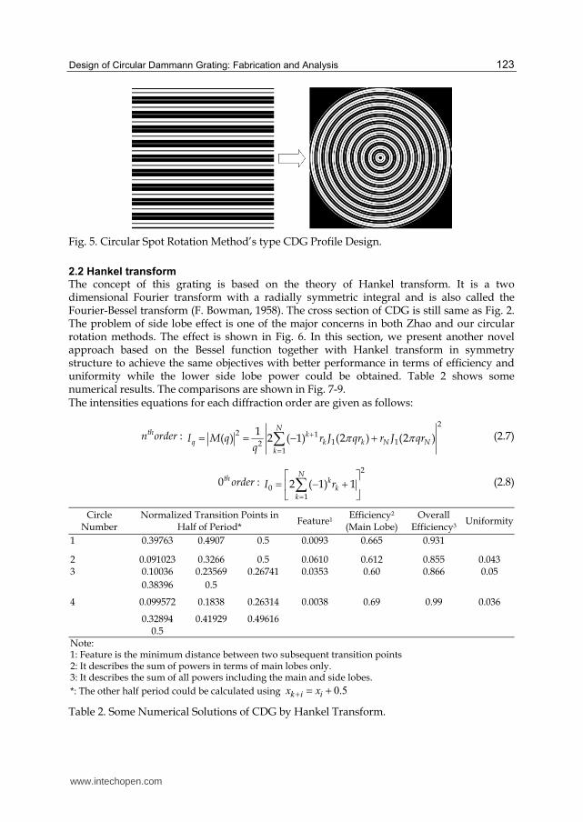
2.1 Circular spot rotation method The concept of generating CDG using this method is based on the theory of conventional Dammann Grating (C. Zhou & L. Liu, 1995). The cross section and first order spectrum of CDG is shown in Fig. 2 and 3 respectively. We assumed that if the diffraction spots rotate 360 degrees continuously, circular rings will be formed. Fig. 4 and 5 illustrate these ideas. Table 1 shows some numerical results. For the formula of Circular Dammann Grating, the intensities among different orders will then be as follows:
:thn order 2 2 22 2
1 1
1( ) {[ ( 1) cos(2 )] [ ( 1) sin(2 )] }
N Nk k
n k kk k
P M n nr nrn
π ππ = == = − + −∑ ∑ (2.1)
0 :th order
2
01
2 ( 1) 1N
kk
k
P r=
⎡ ⎤= − +⎢ ⎥⎣ ⎦∑ (2.2)
The overall normalized efficiency is therefore given as,
2 1n
n
nPη ∞−=−∞
= ∑ (2.3)
The feature size, which is the minimum distance between two different continuous transition points, is
1min k kr r+Δ = − (2.4)
The uniformity is defined as,
max( ) min( )
max( ) min( )n n
n n
I Iuni
I I
−= + (2.5)
The radius (R) of each ring with the focal length (f) of converging lens will then be
n
nR f
D
λ= (2.6)
The numerical solutions with near optimum efficiency and uniformity of CDG are listed in Table 1.
Circle number
Normalized Transition Points in Half of Period*
Efficiency Uniformity Feature Size
1 0.5 0.81 0 0.5
2 0.20525 0.29067 0.5 0.72 0.00006 0.08542
3 0.11649 0.24024 0.26741 0.38396 0.74 0.0002 0.02717
0.5
4 0.099104 0.18382 0.26295 0.32925 0.8 0.00014 0.00508
0.4196 0.49492 0.5
*The other half period could be calculated using 0.5k i ix x+ = +
Table 1. Some Numerical Solutions of CDG by Spot Rotation Method.
www.intechopen.com

Advances in Unconventional Lithography
122
Fig. 2. Cross Section of CDG.
Fig. 3. First order CDG spectrum.
Fig. 4. Concept of Circular Spot Rotation Method’s type CDG.
www.intechopen.com
Design of Circular Dammann Grating: Fabrication and Analysis
123
Fig. 5. Circular Spot Rotation Method’s type CDG Profile Design.
2.2 Hankel transform The concept of this grating is based on the theory of Hankel transform. It is a two dimensional Fourier transform with a radially symmetric integral and is also called the Fourier-Bessel transform (F. Bowman, 1958). The cross section of CDG is still same as Fig. 2. The problem of side lobe effect is one of the major concerns in both Zhao and our circular rotation methods. The effect is shown in Fig. 6. In this section, we present another novel approach based on the Bessel function together with Hankel transform in symmetry structure to achieve the same objectives with better performance in terms of efficiency and uniformity while the lower side lobe power could be obtained. Table 2 shows some numerical results. The comparisons are shown in Fig. 7-9. The intensities equations for each diffraction order are given as follows:
:thn order2
2 11 12
1
1( ) 2 ( 1) (2 ) (2 )
Nk
q k k N Nk
I M q r J qr r J qrq
π π+=
= = − +∑ (2.7)
0 :th order2
01
2 ( 1) 1N
kk
k
I r=
⎡ ⎤= − +⎢ ⎥⎣ ⎦∑ (2.8)
Circle Number
Normalized Transition Points in Half of Period*
Feature1 Efficiency2
(Main Lobe)Overall
Efficiency3 Uniformity
1 0.39763 0.4907 0.5 0.0093 0.665 0.931
2 0.091023 0.3266 0.5 0.0610 0.612 0.855 0.043 3 0.10036 0.23569 0.26741 0.0353 0.60 0.866 0.05
0.38396 0.5
4 0.099572 0.1838 0.26314 0.0038 0.69 0.99 0.036
0.32894 0.41929 0.49616 0.5
Note: 1: Feature is the minimum distance between two subsequent transition points 2: It describes the sum of powers in terms of main lobes only. 3: It describes the sum of all powers including the main and side lobes.
*: The other half period could be calculated using 0.5k i ix x+ = +
Table 2. Some Numerical Solutions of CDG by Hankel Transform.
www.intechopen.com

Advances in Unconventional Lithography
124
Fig. 6. Side Lobe Effect of CDG.
Fig. 7. Main Lobe Intensities Comparisons among Four Different Methods (Triangle: Zhao’s symmetric method, Dot: Zhao’s asymmetric method, Star: Spot Rotation Method, Cross: Hankel Transform).
www.intechopen.com

Design of Circular Dammann Grating: Fabrication and Analysis
125
Fig. 8. Side Lobe Intensities Comparisons among Three Different Methods (Triangle: Zhao’s symmetric method, Dot: Zhao’s asymmetric method, Star: Spot Rotation Method, Cross: Hankel Transform).
Fig. 9. Uniformities Comparisons among Three Different Methods (Triangle: Zhao’s symmetric method, Dot: Zhao’s asymmetric method, Star: Spot Rotation Method, Cross: Hankel Transform).
www.intechopen.com

Advances in Unconventional Lithography
126
The overall normalized efficiency, feature size, uniformity and radius are defined same as equations 2.3-2.6. Side lobe is existed around the main lobe in every diffracted order, is shown in Fig. 6, no matter which method is applied. It is because our design is not able to fully express the concept of circular phase modulation, as the circular profile can not be completely decomposed into a square pixel representation and also finite number of periods happened in practical case. Thus side lobe existed. The lobe separation is not only governed by number of period (ND), but also controlled by the input wavelength and the focal length of the lens. With the assistance of diffraction theory, the final equation is then defined, i.e.
2
3s f
ND
λ= (2.9)
Fig. 10-12 shows this relationship. From these figures, we can conclude that 100 periods is the optimum solution.
Fig. 10. Number of Period against efficiency.
www.intechopen.com

Design of Circular Dammann Grating: Fabrication and Analysis
127
Fig. 11. Number of period against beam width (FWHM).
Fig. 12. Number of Period against separation between two lobes.
www.intechopen.com

Advances in Unconventional Lithography
128
3. Fabrication
Many different fabrication methods exist for diffraction grating. Most of these techniques can be grouped into two main categories: lithographic techniques and electron beam writing. Lithographic techniques (J. Turunen, A Vasara, J Westerholm, G Jin and A Salin, 1990) use light sensitive polymers at the top of the substrate along with controlled etching or deposition methods. For standard e-beam lithography (Masato Okano, Hisao Kikuta, Yoshihiko Hirai, Kazuya Yamamoto, and Tsutom Yotsuya, 2004), an e-beam exposure contains enough of an electron dose that the exposed regions of e-beam resist are fully cleared during the development process. This can be used to produce different thicknesses of e-beam resist simply by varying the dose. The e-beam approach can generate the finest features, a serval tens of nm. However, because of the small size of the electron beam, it is extremely time consuming to expose a pattern of large size of sample.
3.1 Chemical etching fabrication
In previous sections, we have understood the fundamental theories of diffraction and a number of design approaches for CDG. To fabricate these gratings, we have to maintain the desired grating shape which is critical to guarantee high transmission of the order of interest. An optimal depth is very important since existing zero order transmission will happen afterwards. Other defeats, such as mask misalignment, sharpness of the profile, will scatter light to higher orders. Because of the size of the features and the need for flexibility of fabrications, lithographic method is an optimal for many types of DOE fabrication [M. T. Gale, 1997; J. M. Miller et al, 1993; C. Zheng, 2005). A simplified version of the photolithographic processing sequence is shown in Fig. 13.
Fig. 13. Flow Diagram of chemical etching.
Once we confirm the pattern which is determined from the design process, the depth of the diffractive phase structure, which is determined by the wavelength of the incident light and the refractive indices of the substrate and surrounding material, can be calculated. The depth can be calculated by
www.intechopen.com

Design of Circular Dammann Grating: Fabrication and Analysis
129
( )1 02h
n n
λ= − (3.1)
where λ is the input wavelength and 1n , 0n are the indices of refraction of the substrate
material and the surrounding medium at the operating wavelength respectively. The
substrate in using is quartz and the refractive index is shown in Fig. 14.
Fig. 14. Refractive Index of quartz.
Most lithographic masks are binary transmission masks. That is, they contain alternating clear and opaque areas. The opaque areas mean the Chromium remains on top of the substrate. These masks are usually made by forming the pattern in a light-sensitive photoresist on top of thin chrome later on the glass mask. Once the photoresist is developed, the chrome, where the photoresist has been removed, was protected. The mask pattern is exposed using optical pattern generators with controllable beam size. A variety of file formats, e.g. GDSII, CIF and BMP, can be used. The machine in our lab is “Microtech LW405”. The positioning accuracy is 1um and the minimum linewidth is 0.8um. These patterns are transformed into pixel forms with a given dimension and the magnified mask pattern is shown in Fig. 15. The accuracy of patterning curve is related to the wavefront error introduced by the required shape approximation. Increasing the number of pixels can help to improve the accuracy. However, as we expect, the higher degree of accuracy can result of more time spending and the amount of data is also increased. Once the mask is fabricated, which is shown in Fig. 16, we can move on to the next step.
www.intechopen.com

Advances in Unconventional Lithography
130
Fig. 15. Magnified CDG pattern.
Fig. 16. CDG Pattern with the number of periods 100.
Photolithographic methods are based on the use of photoresist create relief structures on
substrate surfaces. This structure is used to protect the underlying substrate during
subsequent processing steps. Photoresists, which is light sensitive polymer, can be either
positive, where the exposed resist dissolves, or they can be negative, where the exposed
resist remains after development. Positive photoresists (e.g. SPR6112B) is used in the
following processing example. After substrate is cleaned, the first step is to coat the
substrate with a thin (typically microns) layer of photoresist. It can be generated by spin coat
www.intechopen.com
Design of Circular Dammann Grating: Fabrication and Analysis
131
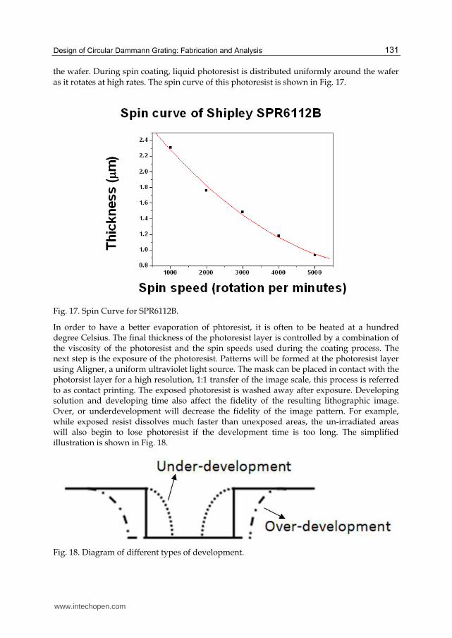
the wafer. During spin coating, liquid photoresist is distributed uniformly around the wafer
as it rotates at high rates. The spin curve of this photoresist is shown in Fig. 17.
Fig. 17. Spin Curve for SPR6112B.
In order to have a better evaporation of phtoresist, it is often to be heated at a hundred degree Celsius. The final thickness of the photoresist layer is controlled by a combination of the viscosity of the photoresist and the spin speeds used during the coating process. The next step is the exposure of the photoresist. Patterns will be formed at the photoresist layer using Aligner, a uniform ultraviolet light source. The mask can be placed in contact with the photorsist layer for a high resolution, 1:1 transfer of the image scale, this process is referred to as contact printing. The exposed photoresist is washed away after exposure. Developing solution and developing time also affect the fidelity of the resulting lithographic image. Over, or underdevelopment will decrease the fidelity of the image pattern. For example, while exposed resist dissolves much faster than unexposed areas, the un-irradiated areas will also begin to lose photoresist if the development time is too long. The simplified illustration is shown in Fig. 18.
Fig. 18. Diagram of different types of development.
www.intechopen.com

Advances in Unconventional Lithography
132
The wafer has been normally spin coated with Chromium with SiO2 as the substrate. This material can be functioned from the ultraviolet through the near infrared due to its own transmission properties and low coefficient of thermal expansion. Normally, a photoresist pattern serves as a wall that protects the area under the photoresist during etching. In our experience, a single photoresist layer without any other protection cannot stand for a long period of time. In this case, we add one more chromium layer which the purpose is same as photoresist. As a result, only the areas not covered by the chromium are removed during the etching process. The wet etching technique is isotropic, which its definition is the etching rate is equal in all directions. This desires for our grating case, particularly for applications requires sharply defined and vertical features. Standard diffractive etch chemistries for silica, usually HF acid, can act as an etching solution. In our experiment, we use another solution, named as Fluorosilicic acid. This etching solution offers a straightforward way to create smooth features in glass materials. In addition fluorosilicic acid etching is considerably safer than conventional hydrofluoric acid (HF) etching. Normally, the temperature controlled heating stage was set at 60°C, which gave an etching solution temperature of 30°C (+0.5°C). Fluorosilicic acid, 100 ml (20% concentration) was allowed to obtain an etch rate 56 nm/min in our experience.
3.2 Electron beam lithography Electron beam lithography (EBL) is based on the principle that some polymers are sensitive to electrons and can be patterned by electron exposure, which is very much like the other lithography. PMMA (Poly Methyl Methacrylate) is normally used in EBL. Its own low exposure time and low resolution are the limitations for our case. We therefore shifted to another resist named “ZEP 520A” by ZEON corporation. ZEP520A is high performance positive EB resists which show high resolution and dry etch resistance. The spin curve and refractive index of this resist are shown in Fig. 19 and 20. The schematic of electron beam system is shown in Fig. 21.
Fig. 19. Spin Curve for ZEP520A with Dilution Rate (provided by ZEON).
www.intechopen.com

Design of Circular Dammann Grating: Fabrication and Analysis
133
Fig. 20. Refractive Index of ZEP520A (provided by ZEON).
Fig. 21. Simplified System of EBL.
www.intechopen.com

Advances in Unconventional Lithography
134
At the top, it consists of an electron gun, a condenser lens to allow changes in the current and corresponding beam diameter, an objective lens to focus the beam on the wafer and a deflector to scan the e-beam around within the field. The sample is placed below on a motorized stage so that it can be patterned by the desired profile. More detailed descriptions of the different types of sources, lenses and the various other components can be found in many textbooks (C. Zheng, 2005). The simplified flow diagram is shown in Fig. 22. The CDG sample is also shown in Fig. 23. The machine in our lab is “Crestec CABL-9510C”.
Fig. 22. Flow diagram of EBL.
Fig. 23. CDG sample using EBL.
www.intechopen.com

Design of Circular Dammann Grating: Fabrication and Analysis
135
4. Conclusion
CDG is affected by the different errors, such as etched depth errors, feature errors, grating period deviations and non vertical side wall angle. Most of these errors will affect the distribution of light into diffracted order. The effects of variation in phase depth and grating duty cycle for a grating are shown in Fig. 24-26 respectively. In general, from the following figures, we can conclude that for getting over 60% efficiency, 100nm variation is allowed in both techniques.
Fig. 24. Etched Depth against efficiency with photolithography.
Fig. 25. Etched Depth against efficiency with EBL.
www.intechopen.com

Advances in Unconventional Lithography
136
Fig. 26. Duty Cycle against efficiency.
Although fabrication errors on these structures will redistribute the energy among diffraction orders and increase the efficiency of central order, the total energy remains the same. It is also noted that the choice of fabrication method introduce different errors. For example, EBL tends to have variations in exposure dosage which has excess etch depth and shape errors. But it can provide very fine width and vertical shape walls and hence it can support high density structure. Conversely, chemical etching technique can provide very sharp side walls and accurate etch depth with carful timing. But, it never supports high density structure as the linewidth it can sustain is in order of um. The users must to balance between the cost and performance requirements.
5. Acknowledgement
This project is supported by GRF (No. 112710) of the Research Grant Council in Hong Kong.
6. References
[1] E. Hecht (2002). Optics, Addison Wesley, ISBN 0-80-538566-5, US [2] C. B. Burckhardt (1966). Diffraction of a plane wave at a sinusoidally stratified dielectric
grating. J. Opt. Soc. Am. Vol. 56 pp.1502–1509, ISSN 0030-3941 [3] M. G. Moharam & T. K. Gaylord (1982). Diffraction Analysis of Dielectric Surface Relief
Gratings. Journal of the Optical Society of America, Vol. 72, pp.1385-1392, ISSN 0030-3941
[4] H. Dammann & K. Gortler (1971). High-efficiency in line multiple imaging by means of multiple phase holograms. Optics Communications, Vol.3, pp.312-315, ISSN 0030-4018
www.intechopen.com

Design of Circular Dammann Grating: Fabrication and Analysis
137
[5] H. Dammann & E. Klotz (1977). Coherent optical generation and inspection of two-dimensional periodic structures. Optica Acta, Vol.4, pp.505-515, ISSN 0950-0340
[6] J. Jahns et al (1989). Dammann gratings for laser beam shaping. Optical Engineering, Vol.28, pp.1267-1275, ISSN 0091-3286
[7] J. Turunen et al (1990). Optimization and fabrication of grating beam splitters. Journal of Physics D: Applied Physics, Vol.21, pp.102-105, ISSN 0022-3727
[8] J. F. Wen & P. S. Chung (2007). 2D optical splitters with Polymer Optical Fiber Arrays. Journal of Optics A: Pure and Applied Optics, Vol.9, pp.723-727 , ISSN 1464-4258
[9] F. J. Wen & P. S. Chung (2007). Two-dimensional optical splitters with polymer optical fibre arrays. Journal of Optics A: Pure and Applied Optics, Vol.9, pp.723-727, ISSN 1464-4258
[10] J. Jia, C. Zhou & L. Liu (2003). Superresolution technology for reduction of the far-field diffraction spot size in the laser free space communication system. Optics Communications, Vol.228, pp.271-278, ISSN 0030-4018
[11] S. Zhao, J. F. Wen & P. S. Chung (2007). Simple focal length measurement technique with a circular Dammann Grating. Applied Optics, Vol.46, pp.44-49, ISSN 0003-6935
[12] S. Zhao & P. S. Chung (2007). Collimation testing using a circular Dammann grating. Optics Communications,Vol.279, pp.1-6, ISSN 0030-4018
[13] C. Wu et al (1991). Optically pumped surface-emitting DFB GalnAsP/InP lasers with circular grating. Electronics Letters, Vol.27, pp.1819-1821, ISSN 0013-5194
[14] T. Erdogan et al (1992). Circularly-symmetric operation of a concentric-circle grating surface-emitting AlGaAs/GaAs quantum-well semiconductor laser. Applied Physics Letters, Vol.60, pp.1921-1923, ISSN 0003-6935
[15] C. Zhou, J. Jia & L. Liu (2003). Circular Dammann Grating. Optics Letters, Vol.28, pp.2174-2176, ISSN 0146-9592
[16] S. Zhao & P. S. Chung (2007). Design of Circular Dammann Grating, Optics Letters, Vol.31, pp.2387-2389, ISSN 0146-9592
[17] J. F. Wen, S. Y. Law & P. S. Chung (2007). Design of Circular Dammann Grating by employing the Circular Spot Rotation Method. Applied Optics, Vol.46, pp.5452-5455, ISSN 0003-6935
[18] J. F. Wen & P. S. Chung (2008). A new Circular Dammann Grating Using Hankel Transform. Journal Optics A: Pure and Applied Optics, Vol.10, 075306, ISSN 1464-4258
[19] J. F. Wen & P. S. Chung (2008). The use of Circular Dammann Grating for angle measurement. Applied Optics, Vol.47, pp.5197-5200, ISSN 0003-6935
[20] J. F. Wen, Z. Y. Chen, & P. S. Chung (2010). Area measurement at long-distance using a circular Dammann grating. Applied Optics, Vol.49, pp.648-652, ISSN 0003-6935
[21] J. F. Wen, Z. Y. Chen & P. S. Chung (2008). A Novel Distance Measurement Technique based on Optical Fractional Fourier Transform, Proceedings of 13th Opto-Electronics and Communications Conference, P-42, ISBN 978-0-85825-807-5, Syndey, Australia, July 7-10, 2008
[22] C. Zhou & L. Liu (1995). Numerical study of Dammann array illuminators. Applied Optics, Vol.34, pp.5961-5969, ISSN 0003-6935
[23] F. Bowman (1958). Introduction to Bessel functions. Dover, ISBN 0486604624, New York, USA
[24] J. Turunen et al (1990). Optimization and fabrication of grating beam splitters. Journal of Physics D, Vol. 21, pp.102-105, ISSN 0022-3727
www.intechopen.com

Advances in Unconventional Lithography
138
[25] Masato Okano et al (2004). Optimization of Diffraction Grating Profiles in Fabrication by Electron-Beam Lithography. Appl. Opt., Vol. 43, pp. 5137-5142, ISSN 0003-6935
[26] M. T. Gale (1997). Replication, In: Binary optics fabrication in Micro-optics: Elements, Systems and Applications, H. P. Herzig (Ed.), Taylor and Francis, ISBN 0748404813, London, England
[27] J. M. Miller et al (1993). Multilevel grating array generators: fabrication error analysis and experiments. Applied Optics, Vol.32, pp.2519-2525, ISSN 0003-6935
[28] C. Zheng (2005). Micro-Nanofabricaton Technologies and Applications, Springer, ISBN 7-04-017663-7, China
www.intechopen.com

Advances in Unconventional LithographyEdited by Dr. Gorgi Kostovski
ISBN 978-953-307-607-2Hard cover, 186 pagesPublisher InTechPublished online 09, November, 2011Published in print edition November, 2011
InTech EuropeUniversity Campus STeP Ri Slavka Krautzeka 83/A 51000 Rijeka, Croatia Phone: +385 (51) 770 447 Fax: +385 (51) 686 166www.intechopen.com
InTech ChinaUnit 405, Office Block, Hotel Equatorial Shanghai No.65, Yan An Road (West), Shanghai, 200040, China
Phone: +86-21-62489820 Fax: +86-21-62489821
The term Lithography encompasses a range of contemporary technologies for micro and nano scalefabrication. Originally driven by the evolution of the semiconductor industry, lithography has grown from itsoptical origins to demonstrate increasingly fine resolution and to permeate fields as diverse as photonics andbiology. Today, greater flexibility and affordability are demanded from lithography more than ever before.Diverse needs across many disciplines have produced a multitude of innovative new lithography techniques.This book, which is the final instalment in a series of three, provides a compelling overview of some of therecent advances in lithography, as recounted by the researchers themselves. Topics discussed includenanoimprinting for plasmonic biosensing, soft lithography for neurobiology and stem cell differentiation,colloidal substrates for two-tier self-assembled nanostructures, tuneable diffractive elements usingphotochromic polymers, and extreme-UV lithography.
How to referenceIn order to correctly reference this scholarly work, feel free to copy and paste the following:
Fung Jacky Wen and Po Sheun Chung (2011). Design of Circular Dammann Grating: Fabrication andAnalysis, Advances in Unconventional Lithography, Dr. Gorgi Kostovski (Ed.), ISBN: 978-953-307-607-2,InTech, Available from: http://www.intechopen.com/books/advances-in-unconventional-lithography/design-of-circular-dammann-grating-fabrication-and-analysis