design of broadband high-efficiency power amplifiers based
TRANSCRIPT

Design of broadbandhigh-efficiency poweramplifiers based on theharmonic-tuned
Xuefei Xuan+ and Fei Yanga)+
State Key Laboratory of Millimeter Waves, Southeast University,
Nanjing 210096, China
Abstract: A novel methodology for designing broadband high-efficiency
power amplifiers (PAs) based on the harmonic-tuned is presented in this
letter. All harmonics can be effectively manipulated by the innovative
structure to achieve high-efficiency and the dual frequencies point harmonic
matching method is also applied to the harmonic control network, which has
a positive effect on the expansion bandwidth. To verify the validity of the
proposed methodology, a gallium nitride PA is designed, implemented, and
measured. Measured results manifest a wide bandwidth from 1.1 to 2.5GHz,
with drain efficiency (DE) of 67–86%, saturated output power greater than
39.5 dBm, and large signal gain larger than 9.5 dB. The in-band second and
third harmonic suppression levels are maintained at −13 to −36 dBc and −23to −44 dBc, respectively. Measurement results confirm the theoretical find-
ings reported in this paper.
Keywords: high-efficiency, broadband, harmonic-tuned, dual frequencies
point harmonic matching, power amplifiers
Classification: Microwave and millimeter-wave devices, circuits, and
modules
References
[1] Z. Cheng, et al.: “High efficiency broadband GaN HEMT power amplifierbased on three-frequency point matching method,” Microw. Opt. Technol. Lett.59 (2017) 1850 (DOI: 10.1002/mop.30634).
[2] W. Luo, et al.: “Design of broadband power amplifier based on a series ofnovel continuous inverse modes,” Electron. Lett. 53 (2017) 685 (DOI: 10.1049/el.2017.0674).
[3] T. Sharma, et al.: “Broadband GaN class-E power amplifier for load modulateddelta sigma and 5G transmitter applications,” IEEE Access 6 (2018) 4709(DOI: 10.1109/ACCESS.2017.2789248).
[4] Z. Cheng, et al.: “A Doherty power amplifier with extended efficiency andbandwidth,” IEICE Electron. Express 14 (2017) 20170188 (DOI: 10.1587/elex.14.20170188).
[5] S. C. Cripps: RF Power Amplifiers for Wireless Communications (ArtechHouse, Norwood, MA, USA, 1999).
+These authors contributed equally to this work.
© IEICE 2018DOI: 10.1587/elex.15.20180980Received October 29, 2018Accepted November 20, 2018Publicized December 7, 2018Copyedited December 25, 2018
1
LETTER IEICE Electronics Express, Vol.15, No.24, 1–9

[6] T. Sharma, et al.: “High-efficiency input and output harmonically engineeredpower amplifiers,” IEEE Trans. Microw. Theory Techn. 66 (2018) 1002 (DOI:10.1109/TMTT.2017.2756046).
[7] N. Tuffy, et al.: “A simplified broadband design methodology for linearizedhigh-efficiency continuous class-F power amplifiers,” IEEE Trans. Microw.Theory Techn. 60 (2012) 1952 (DOI: 10.1109/TMTT.2012.2187534).
[8] T. Canning, et al.: “Continuous mode power amplifier design using harmonicclipping contours: Theory and practice,” IEEE Trans. Microw. Theory Techn.62 (2014) 100 (DOI: 10.1109/TMTT.2013.2292675).
[9] M. Yang, et al.: “Highly efficient broadband continuous inverse class-F poweramplifier design using modified elliptic low-pass filtering matching network,”IEEE Trans. Microw. Theory Techn. 64 (2016) 1515 (DOI: 10.1109/TMTT.2016.2544318).
[10] C. Huang, et al.: “Design of broadband high-efficiency power amplifiers basedon the hybrid continuous modes with phase shift parameter,” IEEE Microw.Wireless Compon. Lett. 28 (2018) 159 (DOI: 10.1109/LMWC.2017.2787061).
[11] S. Y. Zheng, et al.: “Design of ultrawideband high-efficiency extended con-tinuous class-F power amplifier,” IEEE Trans. Ind. Electron. 65 (2018) 4661(DOI: 10.1109/TIE.2017.2772163).
1 Introduction
With the evolution of the modern wireless communication technology, communi-
cation systems is required to have higher efficiency and wider operation bandwidth
[1, 2]. The PA, as one of the most crucial components in the system, is also
requested to have the ability of working in multiband. Meanwhile, since the PA is
an important energy consumer, the efficiency of the whole system is largely
determined by the efficiency of the PA [3, 4]. Recently, the harmonic-tuned PAs
have caused public concern because it is one of key technologies to improve the
efficiency. However, there are two limitations in the traditional harmonic-tuned
PAs, one is the limited orders of harmonics-tuned, which leads to the blocked
efficiency improvement, and the other is the narrowband characteristics of
the harmonic control network severely restrict the bandwidth, such as traditional
Class-F [5] and inverse Class-F [6].
To overcome the above mentioned narrowband problem, a series of continuous
modes are proposed, like continuous Class-F [7], continuous Class-B/J [8], and
continuous inverse Class-F [9], which have a positive effect on the expansion
bandwidth. Nevertheless, the continuous modes are still unable to control higher
order harmonics, so the efficiency cannot be further improved.
In order to achieve both efficiency improvement and bandwidth expansion, a
methodical design approach is presented to design a broadband high-efficiency PA
which employs a novel topology to manipulate all harmonics and dual frequencies
point harmonic matching method is implemented to the harmonic control network.
For the purpose of validation, a high-efficiency and broadband PA is designed
and fabricated over the frequency band of 1.1–2.5GHz with a relative bandwidth
of 78%. The designed PA realizes drain efficiency greater than 67% and the
86% can be attained in the highest point. The experimental results reveal that
© IEICE 2018DOI: 10.1587/elex.15.20180980Received October 29, 2018Accepted November 20, 2018Publicized December 7, 2018Copyedited December 25, 2018
2
IEICE Electronics Express, Vol.15, No.24, 1–9

the performance of PA is superior to traditional harmonic-tuned and continuous
modes.
2 Design of broadband high-efficiency PA
2.1 The theory of harmonic-tuned
According to the theory of harmonic-tuned [5], high-efficiency PA operation is
achieved by saturating the device and manipulating the generated harmonics in
such a manner as to produce nonoverlapping drain waveforms. Harmonics effect on
drain voltage waveform is drawn in Fig. 1. It is clear that the effect of the adding
harmonics is basically to shape voltage waveform changed from sinusoidal to
square wave. It can be seen from the Fig. 1 that the higher order harmonics are
manipulated, and there are better effects of voltage waveform shaping.
For instance, as a typical harmonic-tuned PA, Class-F operation demands open-
circuit terminations at odd harmonics, with short-circuit terminations at the even
harmonics [5]. These waveforms are described by the following equations:
iDðtÞ ¼ I0 þX2��¼1
I� � cosð�!t þ ��Þ k ¼ 1; 2; 3 . . . ð1Þ
VDSðtÞ ¼ VDD �X2�þ1m¼1
Vm � cosðm!t þ �mÞ: k ¼ 1; 2; 3 . . . ð2Þ
where �� and �m are the phases of the output current and voltage at the δth and mth
order, respectively.
Base on the above definition, the DC and drain dissipation of transistors can be
calculated as follows:
PDC ¼ VDD � I0 ð3Þ
Pdiss ¼ 1
T
ZT0
vDSðtÞ � iDðtÞdt: ð4Þ
Fig. 1. Harmonics effect on drain voltage waveform. (m is consistentwith the variables in Eq. (2))
© IEICE 2018DOI: 10.1587/elex.15.20180980Received October 29, 2018Accepted November 20, 2018Publicized December 7, 2018Copyedited December 25, 2018
3
IEICE Electronics Express, Vol.15, No.24, 1–9

The power of each harmonic can be determined as follow:
Pout:nf1¼ 1
2� VnIn � cosð’nÞ: ð5Þ
where n is the order of the harmonics. Therefore, the drain efficiency can be
calculated as follows:
�drain ¼ Pout:f1
PDC¼ Pout:f1
Pdiss þ Pout:f1þX1n¼2
Pout:nf1
: ð6Þ
In Eq. (6), Pdiss is the dissipation caused by the overlap of drain current and voltage
waveforms. So, from the point of view the theory of harmonic-tuned, as long as all
harmonics can be effectively control, each harmonic will not consume energy, and
the drain efficiency of 100% can be achieved.
2.2 Design of harmonic control circuit
Based on the theory of harmonic-tuned and conventional thought of harmonic
control, considering the hardness of matching circuit design and the limited area of
the circuit board, it is very difficulty to manipulate all harmonics. To solve the
above issue, a generic fabric is proposed by utilizing the periodic variation principle
of harmonic impedance.
The presented circuit topology is shown in Fig. 2 and all the parameters are
labeled. First, the design parameters TL1, TL2 and TL3 are chosen as �=4 for the
fundamental frequency. It can be seen from the even harmonics regulation in the
figure that originating from the principle of quarter-wave impedance transforma-
tion, combined with the quarter wavelength short-circuit stub TL1 operating at all
even harmonics, the input impedance of the Zin1 can be determined as follow:
Zin1 ¼ Z2n ¼ jZ1 tan�
2
f2n
f1
� �: n ¼ 1; 2; 3 . . . ð7Þ
where the characteristic impedance of stubs (Z1) is the free design parameters, f2n
is the (2n)th harmonic, Z2n is impedances of even harmonics, and f1 is the
fundamental frequency.
In the odd harmonics regulation section, the quarter wavelength open-circuit
stub TL2 is employed together with a transmission line TL3 operating at all odd
Fig. 2. Circuit design of harmonic control circuit.
© IEICE 2018DOI: 10.1587/elex.15.20180980Received October 29, 2018Accepted November 20, 2018Publicized December 7, 2018Copyedited December 25, 2018
4
IEICE Electronics Express, Vol.15, No.24, 1–9

harmonics. Thus, the input impedances of the ZA and Zin2 can be determined
separately, as follows:
ZA¼ �j Z2
tan
��
2
f2nþ1f1
� n ¼ 1; 2; 3 . . . ð8Þ
Zin2 ¼ Z2nþ1 ¼ jZ3 tan�
2
f2nþ1f1
� �: n ¼ 1; 2; 3 . . . ð9Þ
Similarly, the characteristic impedance (Z2 and Z3) of transmission line are the free
design parameters, f2nþ1 is the (2n+1)th harmonic, Z2nþ1 is impedances of odd
harmonics, and f1 is the fundamental frequency.
Based on Eq. (7) (9), it can be concluded that the impedances of even
harmonics is matched to zero, odd harmonics to infinite. Therefore, the impedances
of all harmonics can be calculated as follows:
Z2n ¼ 0
Z2nþ1 ¼ 1
(: n ¼ 1; 2; 3 . . . ð10Þ
2.3 Broadband high-efficiency matching network design
The operation bandwidth is severely limited by employing a high-Q harmonic
control network in traditional harmonic-tuned PAs [5]. Hence, the dual frequencies
point harmonic matching method is proposed to make up for the imperfection, in
this letter. To expand the bandwidth, two frequency points 1.5GHz and 2.1GHz are
selected to design output matching the harmonic control circuit, respectively.
Meanwhile, using a approach of stepped-impedance matching for fundamental
frequency, the input matching network is also put forward. The broadband high-
efficiency PA including input matching and output matching realized by using
transmission lines is depicted in Fig. 3 and all parameters are labeled.
To validate the feasibility of the proposed design approach, simulated drain
voltage and current waveforms at two frequencies of 1.5GHz and 2.1GHz are
drawn in Fig. 4. These approximately interlaced waveforms manifest the presented
harmonic-tuned is achieved at these frequencies. Meanwhile, in order to further
demonstrate the advantages, the simulated impedance of the second harmonic, third
Fig. 3. Schematic of the broadband high-efficiency PA
© IEICE 2018DOI: 10.1587/elex.15.20180980Received October 29, 2018Accepted November 20, 2018Publicized December 7, 2018Copyedited December 25, 2018
5
IEICE Electronics Express, Vol.15, No.24, 1–9
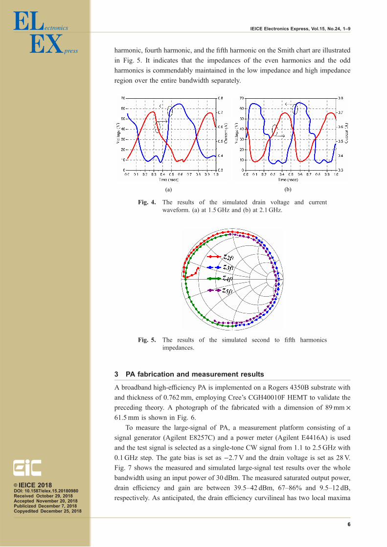
harmonic, fourth harmonic, and the fifth harmonic on the Smith chart are illustrated
in Fig. 5. It indicates that the impedances of the even harmonics and the odd
harmonics is commendably maintained in the low impedance and high impedance
region over the entire bandwidth separately.
3 PA fabrication and measurement results
A broadband high-efficiency PA is implemented on a Rogers 4350B substrate with
and thickness of 0.762mm, employing Cree’s CGH40010F HEMT to validate the
preceding theory. A photograph of the fabricated with a dimension of 89mm �61:5mm is shown in Fig. 6.
To measure the large-signal of PA, a measurement platform consisting of a
signal generator (Agilent E8257C) and a power meter (Agilent E4416A) is used
and the test signal is selected as a single-tone CW signal from 1.1 to 2.5GHz with
0.1GHz step. The gate bias is set as −2.7V and the drain voltage is set as 28V.
Fig. 7 shows the measured and simulated large-signal test results over the whole
bandwidth using an input power of 30 dBm. The measured saturated output power,
drain efficiency and gain are between 39.5–42 dBm, 67–86% and 9.5–12 dB,
respectively. As anticipated, the drain efficiency curvilineal has two local maxima
(a) (b)
Fig. 4. The results of the simulated drain voltage and currentwaveform. (a) at 1.5GHz and (b) at 2.1GHz.
Fig. 5. The results of the simulated second to fifth harmonicsimpedances.
© IEICE 2018DOI: 10.1587/elex.15.20180980Received October 29, 2018Accepted November 20, 2018Publicized December 7, 2018Copyedited December 25, 2018
6
IEICE Electronics Express, Vol.15, No.24, 1–9

at 1.5, and 2.1GHz, which corresponds to the two frequencies selected to the
harmonic matching.
Fig. 8 illustrates measured second to fifth relative harmonics level to funda-
mental frequency output power. When working below 1.3GHz, the second har-
monic is considerable because it falls in the fundamental bandwidth. The harmonic
levels are maintained at −20 to −36 dBc as the favorable harmonic impedances are
provided by harmonic-tuned network at 1.3 to 2.5GHz. The third to fifth harmonic
suppression levels across the band are maintained at −23 to −44 dBc, −28 to
−46 dBc, and −28 to −46 dBc separately. Measured DE, power added efficiency
(PAE), and gain against the corresponding output powers at different operation
frequencies are illustrated in Fig. 9. It can be observed that when the output power
are 40.5 dBm and 42 dBm, the gain is compressed to nearly 3 dB and the
corresponding input is 30 dBm. At the moment, the maximum drain efficiency of
86%, 78.2% and PAE of 81%, 72% are obtained at 2.1GHz and 1.5GHz,
respectively. A comparison with some recently reported broadband high-efficiency
PAs is outlined in Table I and the proposed PA demonstrates outstanding efficiency
performance while its broadband characteristic is comparable with other state-of-
the-art broadband PAs.
Fig. 6. Photograph of the fabricated PA (dimension: 89mm � 61:5mm).
Fig. 7. Measured and simulated DE, output power, and gain across theentire bandwidth.
© IEICE 2018DOI: 10.1587/elex.15.20180980Received October 29, 2018Accepted November 20, 2018Publicized December 7, 2018Copyedited December 25, 2018
7
IEICE Electronics Express, Vol.15, No.24, 1–9

4 Conclusion
In this paper, a systematic method is introduced to design output matching
networks for broadband high-efficiency PAs. Following on from a previous paper,
further novel theory of harmonic-tuned has been presented and combined with the
dual frequencies point harmonic matching method for efficiency enhancement in a
broad bandwidth. The proposed procedure has been demonstrated by implementing
Fig. 8. The results of the measured second to fifth relative harmonicslevel over the entire bandwidth. The results are presentedrelative to the fundamental frequency output power.
Fig. 9. The results of the measured DE, PAE, and gain versus outputpower.
Table I. Comparisons with state-of-the-art broadband PAs
Ref BW (GHz)/RWB (%) DE (%) Power (dBm) Gain (dB) Year
[7] 1.45–2.45/51 70–81 40.4–42.3 10–12.6 2012
[9] 1.35–2.5/60 68–82 41.1–42.5 15.2–17 2016
[10] 1.2–3.6/100 60–72 40–42.2 10.5–12.5 2018
[11] 0.5–2.3/128.5 60–81 39.2–41.2 >11:7 2018
Thiswork
1.1–2.5/78 67–86 39.5–42 9.5–12 2018
© IEICE 2018DOI: 10.1587/elex.15.20180980Received October 29, 2018Accepted November 20, 2018Publicized December 7, 2018Copyedited December 25, 2018
8
IEICE Electronics Express, Vol.15, No.24, 1–9

a PA, based on GaN HEMT device. Measurements of the fabricated amplifier
reveal the PA delivers 8.9–15.8W saturated output power with a DE of 67–86%.
The second and the third harmonic suppression levels are maintained at −13 to
−36 dBc and −23 to −44 dBc, respectively. The simulated and measured results
show good performances on all the indicators.
Acknowledgments
This work is supported by the National Natural Science Foundation of China (Grant
No. 11573007) and the Fundamental Research Funds for the Central Universities
of China (Grant No. 2242018k1G022).
© IEICE 2018DOI: 10.1587/elex.15.20180980Received October 29, 2018Accepted November 20, 2018Publicized December 7, 2018Copyedited December 25, 2018
9
IEICE Electronics Express, Vol.15, No.24, 1–9