design of an analog cmos based interval type-2 fuzzy logic controller chip
TRANSCRIPT

Mamta Khosla, Rakesh Kumar Sarin & Moin Uddin
International Journal of Artificial Intelligence and Expert Systems, Volume (2) : Issue (4) : 2011 167
Design of an Analog CMOS Based Interval Type-2 Fuzzy Logic Controller Chip
Mamta Khosla [email protected] Associate professor Department of Electronics and Communication Engineering Dr B R Ambekdar National Institute of Technology Jalandhar – 144011. India
Rakesh Kumar Sarin [email protected] Professor Department of Electronics and Communication Engineering Dr B R Ambekdar National Institute of Technology Jalandhar – 144011. India
Moin Uddin [email protected] Pro Vice Chancellor Delhi Technological University Delhi – 110042. India
Abstract
We propose the design of an analog Interval Type-2 (IT2) fuzzy logic controller chip that is based on the realization approach of averaging of two Type-1 Fuzzy Logic Systems (T1 FLSs). The fuzzifier is realized using transconductance mode membership function generator circuits. The membership functions are made tunable by setting some reference voltages on the IC pins. The inference is realized using current mode MIN circuits. The consequents are also tunable by providing five reference current sources on chip. Defuzzification of both the T1 FLSs is based on weighted average method realized through scalar and multiplier-divider circuits. An analog current-mode averager circuit is used for obtaining the defuzzified output of the IT2 fuzzy logic controller chip. The chip is designed for two inputs, one output and nine tunable fuzzy rules and is realized in 0.18 µm technology. Cadence Virtuoso Schematic/Layout Editor has been used for the chip design and the performances of all the circuits are confirmed through the simulations carried out using Cadence Spectre tool. The proposed architecture has an operation speed of 20 MFLIPS and a power consumption of 20mW. The whole chip occupies an area of 0.32 mm
2. As
compared to the previous designs, the proposed design has achieved a considerable high speed along with a significant reduction in power and area. Keywords: Type-2 Fuzzy logic Systems, Interval Type-2 Fuzzy Logic Systems, Footprint of Uncertainty, CMOS, Current Mirror.
1. INTRODUCTION
Type-1 fuzzy logic has been the most popular form of fuzzy logic, and has been successfully used in various domains. However, there are various sources of uncertainties facing T1 FLSs, which are usually present in most of the real world applications. T1 FLSs cannot fully model and handle these uncertainties since they use precise and crisp Type-1 Fuzzy Sets (T1 FSs). However, Type-2 Fuzzy Logic Systems (T2 FLSs), which use Type-2 FSs (T2 FSs) characterized by fuzzy membership functions (MFs), have an additional third dimension. This third dimension and Footprint of Uncertainty (FOU) provide additional design degrees of freedom for T2 FLSs to directly model and handle uncertainties [1]. Thus, T2 FLSs are expected to perform better than their traditional counter parts.

Mamta Khosla, Rakesh Kumar Sarin & Moin Uddin
International Journal of Artificial Intelligence and Expert Systems, Volume (2) : Issue (4) : 2011 168
Although T2 FLSs have been used successfully in a number of applications [2-7], their design and implementation is comparatively more difficult, time consuming and slower than T1 FLSs. This is attributed to their much higher computational complexities, difficulty in visualization and use, and non availability of suitable software tools. Thus, the designers cannot reap the benefits of T2 FLSs. Whereas, T1 FLSs are much simpler to design, simulate and realize, and their popularity has been greatly aided by the Graphical User Interface (GUI) based software tools like Fuzzy Logic Toolbox for MATLAB.
Hardware implementation of T1 FLSs is a well-known area [8]. The approaches for implementing these systems cover technologies like microcontrollers, FPGAs, digital and analog VLSI among others [8]-[16]. On the other hand, the hardware realization of T2 FLSs is a relatively nascent research area and a few digital implementations reported in literature have been around microcontrollers, FPGAs etc. [17]-[20]. Digital VLSI implementation was presented by Huang and Chen [21] where the T2 FLS was designed at the transistor level on a single chip based on 0.35 µm technology. Particularly, these implementations have focused on Interval Type-2 Fuzzy Logic Systems (IT2 FLSs), which are a special case of the T2 FLSs and are computationally much simpler than general T2 FLSs. Furthermore, many researchers have validated that IT2 FLS outperforms T1 FLS [2, 22-24].
In this paper, we have designed an analog IT2 fuzzy chip, which is based on the realization methodology of averaging of two T1 FLSs. This methodology has been validated though two case studies by the authors [25] and has also been adopted for the implementation of IT2 FLSs on FPGAs [26, 27]. To the best of our knowledge, there is no report of an analog CMOS based hardware realization of an IT2 FLS in the literature. Analog implementation is superior to digital implementation in terms of processing speed, power dissipation and chip size. The main drawback of analog circuits is their comparatively low accuracy than the digital circuits, which however, is not a severe limitation in view of the typical demands of most fuzzy applications. The main processing stages of the IT2 FLS viz. fuzzification, rule inference, defuzzification all are realized using analog circuits designed in UMC 180 MMRF CMOS (180nm 1P/6M 3.3V) technology. The workings of all the modules are verified through the simulations carried out in Cadence Spectre tool. The synthesis of the modules as a two input, one output, nine rules FLS is simulated and the results demonstrate an inference speed of 20MFLIPS and power consumption of 20mW.
The paper is organized in five sections. Section 2 briefly describes the IT2 FSs and the working of IT2 FLSs. In Section 3, we discuss the design of the IT2 processor in detail; the realization methodology followed for designing IT2 FLS using T1 FLSs is discussed; the circuits of all the analog modules used in the design and their simulation results are presented under this section. In Section 4, the design and performance of analog IT2 fuzzy chip is presented, that has been obtained by combining the various modules presented in Section 3. Finally, Section 5 concludes the paper.
2. OVERVIEW OF IT2 FSS AND IT2 FLSS 2.1 Generalized T2 FSs and Interval T2 FSs A T2 FS can be informally defined as a fuzzy set that is characterized by a fuzzy or non-crisp membership function. This means there is uncertainty in the primary membership grades of a T2 MF, which introduces a third dimension to the MF, defined by the secondary membership grades [28, 29].
Such a T2 FS, denoted by à can be expressed mathematically as in (1)
]}10[,|),(),,{(~
~ ⊆∈∀= xAJXxuxuxA µ (1)

Mamta Khosla, Rakesh Kumar Sarin & Moin Uddin
International Journal of Artificial Intelligence and Expert Systems, Volume (2) : Issue (4) : 2011 169
Where, ),(Ã uxµ is the T2 MF, 1),(0 and ~ ≤≤ uxA
µ ; x, the primary variable, has domain X; u U∈ ,
the secondary variable, has domain xJ at each x X∈ ;
xJ is called the primary membership of x
and ]1,0[⊆∈ xJu
Uncertainty in the primary memberships of a T2 FS consists of a bounded region which is called the Footprint of Uncertainty (FOU). All the embedded FSs of FOU are T1 FSs and their union covers the entire FOU, [1] as in (2)
UXx
xJAFOU∈
=)~
( (2)
IT2 is a special case of a T2 FS where all the secondary membership grades equal one. IT2 FS is completely characterized by its 2-D FOU that is bound by a Lower MF (LMF) and an Upper MF
(UMF), )(~ xA
µ and )(~ xAµ , respectively, both of which are T1 MFs. The FOU of an IT2 FS is
described in terms of these MFs, as in (3).
UXx
AAxxAFOU
∈
= )](),([)~
( ~~ µµ (3)
IT2 FSs are the most widely used T2 FSs to date, used in almost all applications because all calculations are easy to perform. Because of the computational complexity of using a general T2 FLS, most designers only use IT2 FSs in a T2 FLS, the result being an IT2 FLS. LMF and UMF together are popularly used in most of research papers to represent IT2 FLSs [28]. 2.2 Working of IT2 FLS A general block diagram for a T2 FLS is depicted in Fig. 1 [28]. It is very similar to a T1 FLS, the major structural difference being that the defuzzifier block of a T1 FLS is replaced by the Output Processing block in a T2 FLS. This block consists of a Type-Reduction sub-module followed by a Defuzzifier.
FIGURE 1: A T2 FLS block diagram.
An IT2 FLS is an FLS, where all of the consequent and antecedent T2 FSs are IT2 FSs. Hence, the working of an IT2 FLS is also similar to that of a general T2 FLS, as depicted in Fig.1. The IT2 FLS works as follows: the crisp inputs are first fuzzified into IT2 FSs, which then activate the inference engine and the rule base to produce output IT2 FSs. These IT2 FSs are then processed by a type-reducer. Type-reduction basically represents mapping of T2 FS into a T1 FS that is called a type-reduced set. A defuzzifier then defuzzifies the type-reduced set to produce crisp outputs [29].
3. DESIGN OF ANALOG MODULES FOR IT2 FLS 3.1 Realization Methodology for IT2 FLS with T1 FLSs As mentioned in Section II, an IT2 FS can be completely characterized by its 2-D FOU, which in turn can be represented in terms of two T1 FSs. There are two approaches for obtaining these T1 FSs and the corresponding T1 FLSs as shown in Fig 2.

Mamta Khosla, Rakesh Kumar Sarin & Moin Uddin
International Journal of Artificial Intelligence and Expert Systems, Volume (2) : Issue (4) : 2011 170
a) In the first approach, one T1 FLS can be formed with the LMFs of all the input and output IT2 FSs and the second T1 FLS with their corresponding UMFs. UMF and LMF are the outer and inner envelopes of the FOU respectively as shown in Fig 2.
b) In the second approach, one T1 FLS can be obtained with the Left FSs of all the input and output IT2 FSs and the second T1 FLS with their corresponding Right FSs. These Left and Right FSs are represented with bold red and blue lines respectively in Fig 2.
FIGURE 2: FOU of an IT2 FS.
Authors have proposed and validated [25] that IT2 FLS can be realized with the average of two T1 FLSs, where two T1 FLSs were formed based on the first approach as described above. For validation, this methodology was applied on (i) an arbitrary system of two inputs, one output and nine rules, and (ii) the Mackey-Glass time-series forecasting. In the second case study, T1 FLS was evolved using Particle Swarm Optimization (PSO) algorithm for the Mackey-Glass time-series data with added noise, and was then upgraded to IT2 FLS by adding FOU. Further, four experiments were conducted in the second case study for four different noise levels. For each case study, a comparative study of the results of the average of two T1 FLSs and the corresponding IT2 FLS, obtained through computer simulations in MATLAB environment validated that IT2 FLS performance is equivalent to the average of two T1 FLSs; that proves the effectiveness of the realization approach. The design of IT2 fuzzy logic controller chip presented in this paper is based on the architecture shown in Fig. 3. This architecture uses two T1 FLSs to emulate an IT2 FLS and uses the first approach for obtaining two T1 FLSs. Here, the first T1 FLS is constructed using UMFs and the second one with the LMFs so as to emulate the FOUs of all IT2 FSs in an IT2 FLS. The fuzzification, fuzzy inference and defuzzification are done as traditionally for two T1 FLSs and the outputs are then averaged to yield the final output of the IT2 FLS. The advantage of using this realization methodology is that it avoids the complications and intensive computations required for type reduction.
FIGURE 3: Realization Methodology for IT2 FLS with T1 FLSs.
Interval Type-2 FLS
Crisp Input
Type-1 FLS
(UMFs)
Type-1 FLS
(LMFs)
Average Crisp Output

Mamta Khosla, Rakesh Kumar Sarin & Moin Uddin
International Journal of Artificial Intelligence and Expert Systems, Volume (2) : Issue (4) : 2011 171
3.2 Analog Functional Blocks of IT2 FLS In this section, we describe the complete structure of the designed IT2 fuzzy processor in detail. A zero order TSK fuzzy model is used for implementing each T1 FLS i.e. the rule consequents are constant values called singletons and each rule has the format described in (4).
In the above, x and y are input variables, A and B are linguistic variables of x and y, defined by FSs. Furthermore, z is an output variable and c is some constant. The output is computed from a weighted average represented by (5), in which each consequent value zi is weighted by the activation degree wi of its corresponding rule, iα being the weight associated to i
th rule.
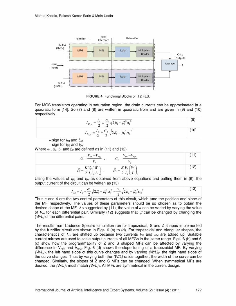
The complete schematic arrangement for the hardware implementation of the IT2 FLS is shown in Fig. 4. It has the following functional blocks:
a) Fuzzifier block fuzzifies the inputs and it contains membership function generators (MFGs) that generate MFs of different shapes viz. Z, trapezoidal, triangle and S.
b) MIN circuit is used in the inference engine for computing the activation degree of each rule.
c) Scalar circuits are used to weight the singleton consequents. d) Multiplier-Divider circuits are used for calculating the defuzzified output of each T1
FLS. e) Averager circuit calculates the defuzzified output of the IT2 processor by computing
the average of the two defuzzified values obtained from both T1 FLSs.
In the present work, an IT2 fuzzy chip for two input variables, partitioned into three FSs, and one output having five singletons is designed. Therefore, each T1 FLS viz. the T1 FLS (UMFs) and the T1 FLS (LMFs), have 2 inputs (3 MFs for each input) and 1 output (5 singletons). We use MIN method for the inference engine of T1 FLSs. For the defuzzification of each T1 FLS, weighted average method is used. Detailed description of the circuits used for each functional block of the IT2 fuzzy chip is given below. 3.2.1 Fuzzifier Circuit [31] Fuzzifier, which converts a crisp input to a fuzzy set, is the first stage in a fuzzy controller. We have used transconductance mode CMOS based circuits for implementing the fuzzifier block and its schematic is shown in Fig. 5. It consists of two differential amplifiers with one PMOS current mirror load. Vref1 and Vref2 are the control voltages that are fed to one input of each differential pair. And VIN is applied to the second inputs of both the differential pairs. Iout can be written as in (6).
IF (x is A) AND (y is B) THEN z = c
(4)
∑
∑=
iii
ii
ii
w
zw
Outputα
α
(5)
42 DDout III += (6)
Since all transistors in this circuit operate in saturation region i.e. VGS>VT and VDS>VGS-VT for each MOS transistor, therefore their drain currents can be defined by (7) and (8).
)( 21 12,1 TGSD VVKI −= (7)
)( 22 24,3 TGSD VVKI −= (8)
parameter uctance transcond theis ,2
)/( ,
2
)/( where 2
21
1 KLWK
KLWK
K ==
ref2INGSref1INGS VVV and VVV21
−=−=
1)/( LW =size of M1 & M2, 2)/( LW =size of M3 & M4
Mamta Khosla, Rakesh Kumar Sarin & Moin Uddin
International Journal of Artificial Intelligence and Expert Systems, Volume (2) : Issue (4) : 2011 172
FIGURE 4: Functional Blocks of IT2 FLS.
For MOS transistors operating in saturation region, the drain currents can be approximated in a quadratic form [14]. So (7) and (8) are written in quadratic from and are given in (9) and (10) respectively.
+ sign for ID1 and ID3 − sign for ID2 and ID4
Where α1, α2, β1 and β2 are defined as in (11) and (12)
Using the values of ID2 and ID4 as obtained from above equations and putting them in (6), the output current of the circuit can be written as (13)
Thus α and β are the two control parameters of this circuit, which tune the position and slope of the MF respectively. The values of these parameters should be so chosen as to obtain the desired shape of the MF. Αs suggested by (11), the value of α can be varied by varying the value of Vref for each differential pair. Similarly (12) suggests that β can be changed by changing the (W/L) of the differential pairs. The results from Cadence Spectre simulation run for trapezoidal, S and Z shapes implemented by the fuzzifier circuit are shown in Figs. 6 (a) to (d). For trapezoidal and triangular shapes, the characteristics of Iout are shifted up because two currents ID2 and ID4 are added up. Suitable current mirrors are used to scale output currents of all MFGs in the same range. Figs. 6 (b) and 6 (c) show how the programmability of Z and S shaped MFs can be affected by varying the difference in Vref1 and Vref2. Fig. 6 (d) shows the slope tuning of a trapezoidal MF. By varying (W/L)1, the left hand slope of this curve changes and by varying (W/L)2, the right hand slope of the curve changes. Thus by varying both the (W/L) ratios together, the width of the curve can be changed. Similarly, the slopes of Z and S MFs can be changed. When symmetrical MFs are desired, the (W/L)1 must match (W/L)2. All MFs are symmetrical in the current design.
222
21
211
12,1
αββα
−±= SD
II
(9)
222
22
222
24,3
αββα
−±= SD
II
(10)
, 2121
T
refIN
T
refIN
V
VV
V
VV −=
−= αα
(11)
2
, 2 2
21
1
=
=
L
W
I
VK
L
W
I
VK
S
T
S
T ββ (12)
22
22
22
222
221
211
1 αββα
αββα
−−−−= Sout II (13)
MFG
MIN
MIN
Scalar
Scalar
T1 FLS (LMFs)
Fuzzifier Rule
Inference Defuzzifier
Crisp Inputs
MFG
Crisp
Outputs
T1 FLS
(UMFs)
Multiplie r-Divider
Multiplie r-Divider
Averager
Mamta Khosla, Rakesh Kumar Sarin & Moin Uddin
International Journal of Artificial Intelligence and Expert Systems, Volume (2) : Issue (4) : 2011 173
FIGURE 5: Membership Function Generator (MFG) circuit.
3.2.2. MIN-MAX Circuits The most popular fuzzy logic operators used to compute the inference of a rule are logical “AND” and logical “OR”. MIN and MAX modules can be used to implement the AND and OR operations respectively. We have used current mode MIN circuits to implement the rule base. One MIN is required for calculating the inference of each rule. The circuit schematics of a two-input MIN is shown in Fig. 7 (a) [16]. It consists of MAX circuit block as shown in Fig. 7 (b) with extra current sources to complement the directions of currents [32]. Transistors M1 and M3 are source follower transistors. M2 and M4 are current sensor transistors that can sink high current. The value of VBias, which is applied to M1, M3 and M5 transistor gates, is calculated from (14).
Where, VGS= Transistor gate-source voltage, and ∆=overdrive voltage
FIGURE 6: (a). Trapezoidal curve obtained through simulation of MFG circuit Vref1=1.5V, Vref2=2V, W/L=5 6(b). S-shaped curve obtained through simulation of MFG circuit Vref1=0V, Vref2=1V, 1.3V,
4,23,1VVV GSBias ∆+= (14)
6(b) 6(a)
6(c) 6(d)

Mamta Khosla, Rakesh Kumar Sarin & Moin Uddin
International Journal of Artificial Intelligence and Expert Systems, Volume (2) : Issue (4) : 2011 174
1.5V, W/L=3 6(c). Z-shaped curve obtained through simulation of MFG circuit Vref2=0V, Vref1=500mV, 1V, 1.5V, W/L=3 6(d). Slope tuning of trapezoidal MF Vref1=1.5V, Vref2=2V, W/L=5,3.
If I1>I2 in the MAX circuit, M1 and M2 transistors will be in the saturation region, M3 and M4 will be in triode and cutoff regions respectively because of current mirror circuits. Thus, M1 current I1 would mirror in to the output. The MIN circuit operation is very similar to the MAX circuit, with the difference that the currents I1 and I2 are being stolen from the transistors M1 and M3. Therefore, in the MIN circuit, the branch from which we steal lesser current would mirror its current into the output. These circuits can work with low power supply; the minimum power supply for these circuits is calculated from (15).
Since there are a large number of MIN circuits used in a fuzzy controller, power consumption of chip will be decreased significantly with these MIN circuits working on low voltage. Size of each MIN depends upon the number of inputs only and we can increase the number of inputs of these circuits only by adding two transistors for each input such as M1 and M2. The design presented here targets 2 inputs, and therefore, two inputs MIN circuits are required. Inputs to each MIN circuit are the outputs of two MFGs from the fuzzifier block, which correspond to the antecedent part of the rule in consideration and the output of each MIN is the firing rule strength wi of that rule. Simulation results of a two input MIN circuit are given in Figs. 8 (a) and (b). Fig. 8 (a) is the DC output characteristic for different values of I2 and Fig. 8 (b) is the transient response for two different shapes of I1 and I2. Fig. 9 (a) and (b) are the DC output characteristics and transient response respectively for a two input MAX circuit.
FIGURE 7 (a): MIN circuit. FIGURE 7 (b): MAX circuit.
FIGURE 8: (a). DC response of MIN circuit with two inputs (b). Transient response of MIN circuit with two inputs
3.2.3. Scalar Circuit Scalar circuit provides many current sources of scaled value of the input current. Scalar circuit is based on current mirror as shown in Fig. 10. Iin is the input current and Io1, Io2,…, Ioi are the output
)(min 2 SatDSGSDD VVV += (15)
7(a) 7(b)
8(b) 8(a)

Mamta Khosla, Rakesh Kumar Sarin & Moin Uddin
International Journal of Artificial Intelligence and Expert Systems, Volume (2) : Issue (4) : 2011 175
currents of 1st, 2
nd, and i
th stage mirrors, respectively. Since, transistor M1 is in saturation region,
Iin can be written as (16).
Current through the ith current mirror can be written as (17).
FIGURE 9: (a). DC response of MAX circuit with two inputs (b). Transient response of MAX circuit with two inputs.
From (16) and (17), Ioi can be simplified to (18).
Where, αi is the scaling factor of the ith stage current mirror, given by (19).
Response of the scalar circuit is shown in Fig. 11 for different values of α (0.5, 1, and 2).
FIGURE 10: Scalar circuit FIGURE 11: Response of Scalar circuit (for α =0.5, 1, and 2).
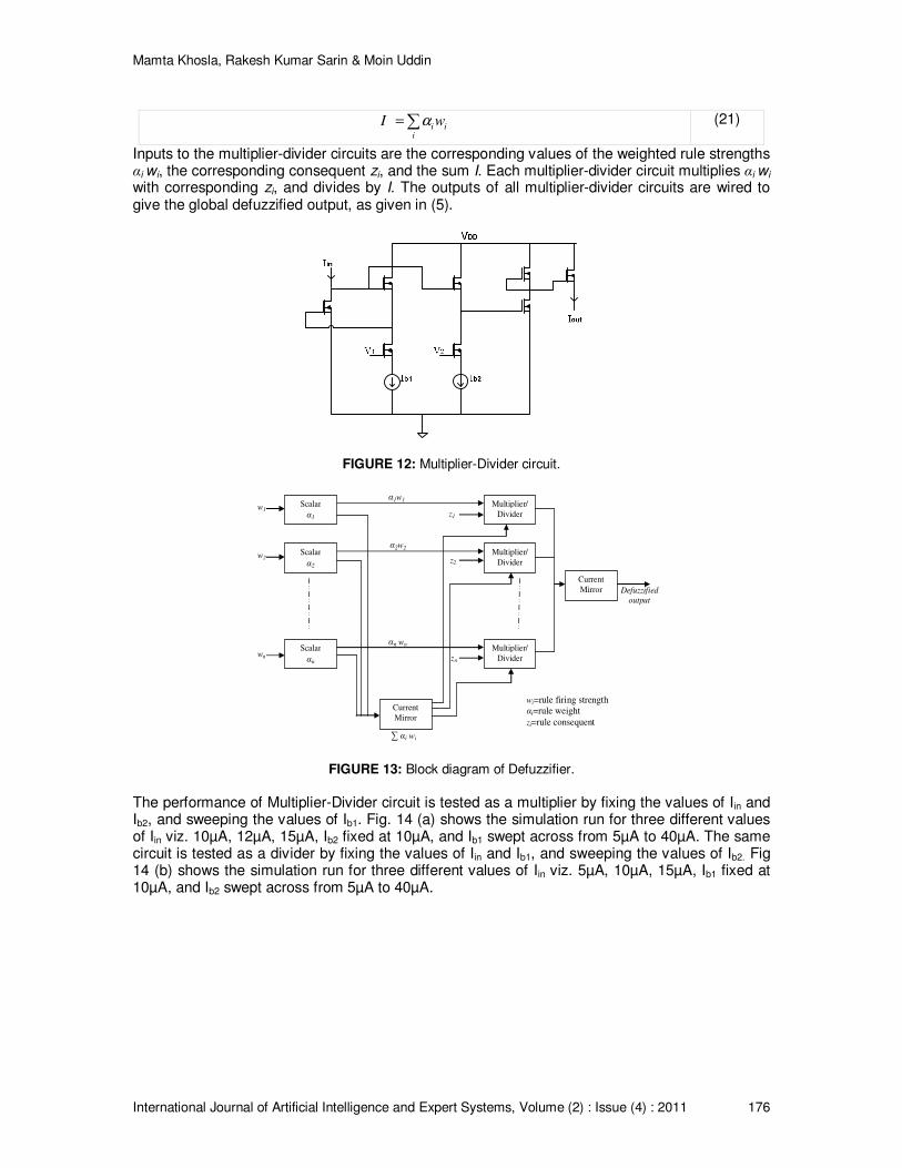
3.2.4. Multiplier-Divider Circuit Multiplier-divider circuit shown in Fig. 12 is used in the defuzzifier section [15]. It works on the principle of translinear circuits where all the transistors are operating in saturation region. The output of the circuit can be expressed as (20)
Block diagram of the defuzzification scheme followed here is shown in Fig. 13. It consists of scalar circuits in the first stage. The scalar takes the rule strength wi calculated from the MIN circuit as the input current, and generates the weighted rule strength αiwi. Outputs of all scalars are wired to produce the sum of these weighted rule strengths. The resultant current output I of the current mirror is given by (21).
2)()/(5.0 TGSinin VVLWKI −= (16)
2)()/(5.0 TGSioi VVLWKI −= (17)
inioi II α= (18)
in
ii
LW
LW
)/(
)/(=α
(19)
2
1
b
binout
I
III =
(20)
9(a) 9(b)
Mamta Khosla, Rakesh Kumar Sarin & Moin Uddin
International Journal of Artificial Intelligence and Expert Systems, Volume (2) : Issue (4) : 2011 176
Inputs to the multiplier-divider circuits are the corresponding values of the weighted rule strengths αi wi, the corresponding consequent zi, and the sum I. Each multiplier-divider circuit multiplies αi wi with corresponding zi, and divides by I. The outputs of all multiplier-divider circuits are wired to give the global defuzzified output, as given in (5).
FIGURE 12: Multiplier-Divider circuit.
Multiplier/Divider
Multiplier/Divider
Multiplier/Divider
Scalar α1
Scalar α2
Scalar αn
Current Mirror
w1
wn
w2
α1w1
α2w2
αn wn
z1
z2
zn
∑ αi wi
Defuzzified
output
Current Mirror
wi=rule firing strength
αi=rule weight zi=rule consequent
FIGURE 13: Block diagram of Defuzzifier.
The performance of Multiplier-Divider circuit is tested as a multiplier by fixing the values of Iin and Ib2, and sweeping the values of Ib1. Fig. 14 (a) shows the simulation run for three different values of Iin viz. 10µA, 12µA, 15µA, Ib2 fixed at 10µA, and Ib1 swept across from 5µA to 40µA. The same circuit is tested as a divider by fixing the values of Iin and Ib1, and sweeping the values of Ib2. Fig 14 (b) shows the simulation run for three different values of Iin viz. 5µA, 10µA, 15µA, Ib1 fixed at 10µA, and Ib2 swept across from 5µA to 40µA.
∑=i
iiwI α (21)

Mamta Khosla, Rakesh Kumar Sarin & Moin Uddin
International Journal of Artificial Intelligence and Expert Systems, Volume (2) : Issue (4) : 2011 177
FIGURE 14: (a). Multiplier-Divider circuit acting as multiplier (Iin =10µA, 12µA, 15µA, Ib2 = 10µA). (b). Multiplier-Divider circuit acting as divider (Iin =5µA, 10µA, 15µA, Ib1 = 10µA).
3.2.5 Averager Circuit The averager circuit computes the average of the defuzzified outputs of two T1 FLSs, which is the final defuzzified output of the IT2 FLS. The averager circuit works on the principle of current mirror. Defuzzified outputs of both the T1 FLSs are wired so that the sum of both becomes the drain current of M1 as shown in Fig. 15 and as represented by (22). Sizes of M1 and M2 are related by (23).
Current output from M2 is the average of the two input currents I1 and I2, where I1 is the output current from T1 FLS (UMFs) and I2 is the output current from T1 FLS (LMFs). Thus, this circuit gives the average of the two T1 FLSs. Fig. 16 shows the simulation result of Averager circuit.
FIGURE 15: Averager circuit FIGURE 16: Response of Averager circuit.
4. ANALOG IT2 FUZZY LOGIC CONTROLLER CHIP In this section, fuzzy functional blocks which have been described in the previous section, are combined into an IT2 fuzzy chip and the arrangement is shown in Fig. 17. Current mirrors are used wherever required to change the current directions. Both T1 FLSs differ only in the designs of their fuzzifiers, specifically, the sizes of the differential pair MOS transistors of the MFGs. For generating two different slopes corresponding to the UMFs and LMFs of the FOUs, W/L=4 and W/L=3 respectively are selected. Designs of all other modules viz. MIN, scalar, defuzzifier are same in both T1 FLSs of the IT2 fuzzy chip.
211 IIID += (22)
12 )/(2
1)/( LWLW =
(23)
Therefore, 2
212
III D
+=
(24)

Mamta Khosla, Rakesh Kumar Sarin & Moin Uddin
International Journal of Artificial Intelligence and Expert Systems, Volume (2) : Issue (4) : 2011 178
FIGURE 17: Arrangement of Fuzzy functional blocks for IT2 Fuzzy Chip realization
FIGURE 18: UMFs and LMFs of 3 FOUs for one variable obtained through simulation of fuzzifier circuit W/L=4 for UMFs, 3 for LMFs
TABLE 1: On-chip Voltage and Current sources.
Inp
ut
1
Outpu
Inp
ut
1
z1
Vref1 Vref2
MFG
Vref1 Vref2
MFG
Vref1 Vref2
MFG
MIN
Vref1 Vref2
MFG
Vref1 Vref2
MFG
Vref1 Vref2
MFG
MIN
MIN
MIN
MIN
MIN
MIN
MIN (3,2) MIN
Scalar – α1
Scalar – α2
Scalar – α3
Scalar – α4
Scalar – α5
Scalar – α6
Scalar – α7
Scalar – α8
Scalar – α9
Multiplier-Divider
z9 Multiplier-Divider
Current Mirror
Cur
rent
Mir
ror
z1
Vref1 Vref2
MFG
Vref1 Vref2
MFG
Vref1 Vref2
MFG
MIN
Vref1 Vref2
MFG
Vref1 Vref2
MFG
Vref1 Vref2
MFG
MIN
MIN
MIN
MIN
MIN
MIN
MIN
MIN
Scalar – α1
Scalar – α2
Scalar – α3
Scalar – α4
Scalar – α5
Scalar – α6
Scalar – α7
Scalar – α8
Scalar – α9
Multiplier-Divider
z9 Multiplier-Divider
Current Mirror
Cur
rent
Mir
ror
Averager
Inp
ut
2
Inp
ut
2
T1 FLS
(UMFs)
T1 FLS
(LMFs)
Current Sources
10µA
20µA
30µA
40µA
50µA
Voltage Sources
0.9V
1.0V
1.2V
2.1V
2.2V
2.4V
2.5V

Mamta Khosla, Rakesh Kumar Sarin & Moin Uddin
International Journal of Artificial Intelligence and Expert Systems, Volume (2) : Issue (4) : 2011 179
LMFs Vref1 Vref2
1 1 5
2 2.2 1.0
3 0 2.4
TABLE 2: Reference Voltage (V) Settings
Pins Details Number of Pins
VDD 1
GND 1 Inputs 2 Output 1 Consequents 5 On-chip Current Sources 5
On-chip Reference Voltage Sources 7 Vref1 and Vref2 for all the MFGs for T1 FLS (UMFs) and T1 FLS (LMFs) 2*[2*3+2*3]
24
Total 46
TABLE 3: External pins of IT2 Fuzzy Logic Controller Chip
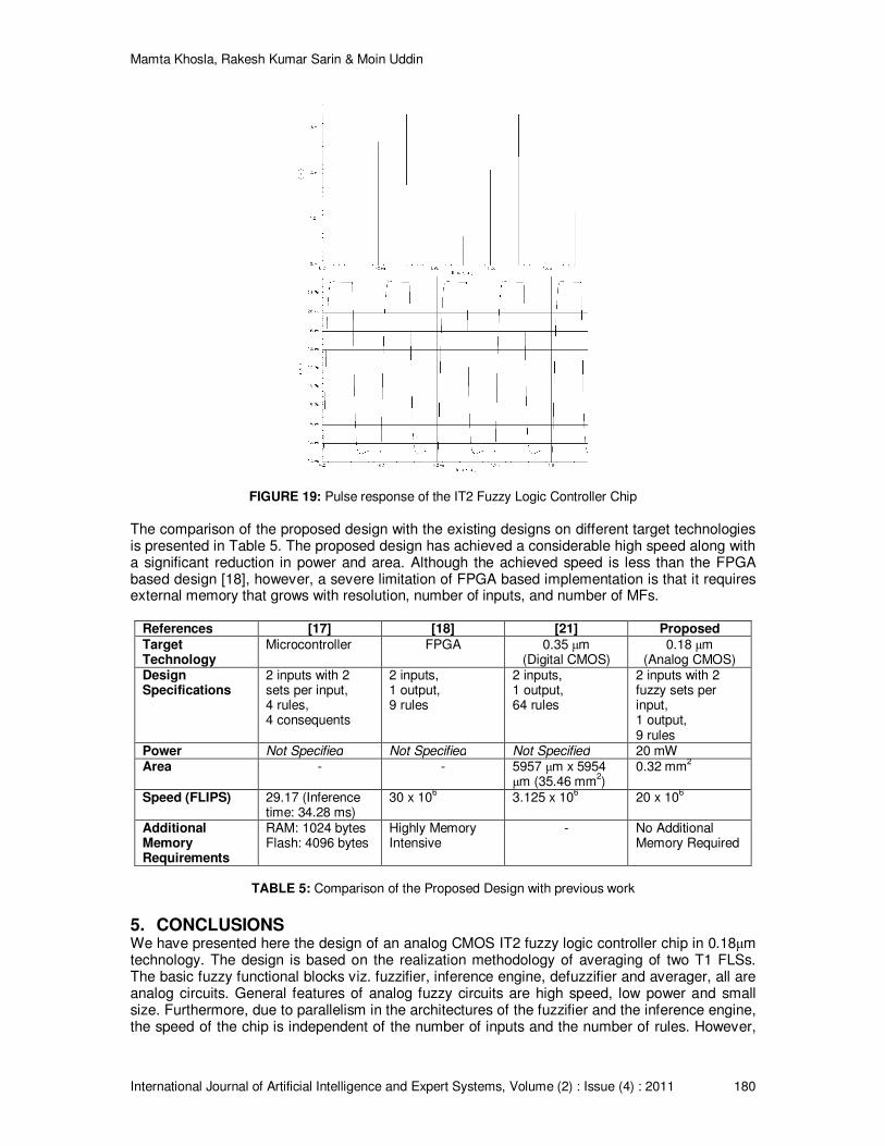
4.1. Pulse Response of IT2 Fuzzy Logic Controller Chip In order to determine the speed of the chip, a square pulse is applied to one input, while the other input is set to 0V. The input MFs for this test are shown in Fig. 18. Rule base for both T1 FLSs is taken arbitrarily and is listed in Table 4 in indexed form. The numbers in the input and output columns refer to the index number of membership functions. Results of this test obtained through Cadence Spectre Simulation are shown in Fig. 19. The response of this chip to pulse input shows a maximum delay of 50ns. This corresponds to a speed of 20 MFLIPS (mega fuzzy logic inferences per second) including the defuzzification process. Since, rule by rule architecture has been followed in this realization; the fuzzy inferences are performed in parallel. Hence, the inference speed is independent of the number of rules and number of MFs. This speed is in a good range for most applications. The chip occupies an area of 0.32 mm
2.
Rule
Number Input
#1 Input
#2 Output
1 1 1 1 2 1 2 2 3 1 3 3
4 2 1 2 5 2 2 3 6 2 3 4 7 3 1 3 8 3 2 4
9 3 3 5
TABLE 4: Fuzzy Rule base in Indexed form
UMFs Vref1 Vref2
1 0.9 5
2 2.1 1.2
3 0 2.5
Mamta Khosla, Rakesh Kumar Sarin & Moin Uddin
International Journal of Artificial Intelligence and Expert Systems, Volume (2) : Issue (4) : 2011 180
FIGURE 19: Pulse response of the IT2 Fuzzy Logic Controller Chip
The comparison of the proposed design with the existing designs on different target technologies is presented in Table 5. The proposed design has achieved a considerable high speed along with a significant reduction in power and area. Although the achieved speed is less than the FPGA based design [18], however, a severe limitation of FPGA based implementation is that it requires external memory that grows with resolution, number of inputs, and number of MFs.
References [17] [18] [21] Proposed
Target Technology
Microcontroller FPGA 0.35 µm (Digital CMOS)
0.18 µm (Analog CMOS)
Design Specifications
2 inputs with 2 sets per input, 4 rules, 4 consequents
2 inputs, 1 output, 9 rules
2 inputs, 1 output, 64 rules
2 inputs with 2 fuzzy sets per input, 1 output, 9 rules
Power Not Specified Not Specified Not Specified 20 mW Area - - 5957 µm x 5954
µm (35.46 mm2)
0.32 mm2
Speed (FLIPS) 29.17 (Inference time: 34.28 ms)
30 x 106 3.125 x 10
6 20 x 10
6
Additional Memory Requirements
RAM: 1024 bytes Flash: 4096 bytes
Highly Memory Intensive
- No Additional Memory Required
TABLE 5: Comparison of the Proposed Design with previous work
5. CONCLUSIONS We have presented here the design of an analog CMOS IT2 fuzzy logic controller chip in 0.18µm technology. The design is based on the realization methodology of averaging of two T1 FLSs. The basic fuzzy functional blocks viz. fuzzifier, inference engine, defuzzifier and averager, all are analog circuits. General features of analog fuzzy circuits are high speed, low power and small size. Furthermore, due to parallelism in the architectures of the fuzzifier and the inference engine, the speed of the chip is independent of the number of inputs and the number of rules. However,

Mamta Khosla, Rakesh Kumar Sarin & Moin Uddin
International Journal of Artificial Intelligence and Expert Systems, Volume (2) : Issue (4) : 2011 181
the power consumption will increase with the number of inputs and the number of MFs used to fuzzify each input. The shapes and positions of the MFs are tunable through IC control pins. The rule base is also programmable through control pins provided on IC. Further some references voltage sources and reference consequent current sources are designed on chip. The chip has a speed of 20 MFLIPS and power consumption of 20mW and it occupies an area of 0.32mm
2. The chip features are
listed in Table 6.
TABLE 6: IT2 Fuzzy Logic Controller Chip Features
6. ACKNOWLEDGMENT We would like to thank Government of India for providing facilities to our institute under SMDP-II project. This work has been carried out using lab facilities created under SMDP-II at Electronics & Communication Engineering Department provided by Ministry of Communication and Information Technology, New Delhi, Government of India.
7. REFERENCES [1] J.M. Mendel and R.I. John, “Type-2 Fuzzy Sets Made Simple”, IEEE Transaction on Fuzzy
Systems, vol. 10, no. 2, 2002, pp. 117–127. [2] Q. Liang and J. M. Mendel, “Equalization of nonlinear time-varying channels using type-2
fuzzy adaptive filters”, IEEE Trans. Fuzzy Syst., vol. 8, no. 5, 2000, pp. 551–563. [3] Q. Liang and J. M. Mendel, “MPEG VBR video traffic modeling and classification using fuzzy
technique”, IEEE Trans. Fuzzy Syst., vol. 9, no. 1, 2001, pp. 183–193. [4] H. B. Mitchell, “Pattern recognition using type-II fuzzy sets,” Inf. Sci., vol. 170, no. 2–4, 2005,
pp. 409–418. [5] J. Zeng and Z. Q. Liu, “Type-2 fuzzy hidden Markov models and their application to speech
recognition”, IEEE Trans. Fuzzy Syst., vol. 14, no. 3, 2006, pp. 454–467. [6] P. Melin and O. Castillo, “A new method for adaptive control of nonlinear plants using type-2
fuzzy logic and neural networks”, J. Gen. Syst., vol. 33, no. 2/3, 2004, pp. 289–304. [7] H. Hagras, “A hierarchical type-2 fuzzy logic control architecture for autonomous mobile
robots”, IEEE Trans. Fuzzy Syst., vol. 12, no. 4, 2004, pp. 524–539. [8] Baturone, Barriga, Carlos Jimenez-Fernandez and Diego, R. Lopez, Microelectronic Design
of Fuzzy-Logic Based Systems, CRC Press, 2000.
Description Features
Technology 0.18µm
No. of Inputs 2 (3 MFs each)
No. of Outputs 1 (5 singletons)
No. of pins 46
Supply Voltage 3.3V
Power Consumption 20 mW
Inference speed 20MFLIPS
Area 0.32mm2
Mamta Khosla, Rakesh Kumar Sarin & Moin Uddin
International Journal of Artificial Intelligence and Expert Systems, Volume (2) : Issue (4) : 2011 182
[9] H. Eichfeld, T. Künemund, and M. Menke, “A 12b general-purpose fuzzy logic controller chip”, IEEE Trans. Fuzzy Syst., vol. 4, no. 4, 1996, pp. 460–475.
[10] M.J. Patyra, J.L. Grantner and K. Koster, “Digital fuzzy logic controller: Design and
implementation”, IEEE Trans. Fuzzy Syst., vol. 4, no. 4, 1996, pp. 439–459. [11] J.M. Jou, P.Y. Chen and S.F. Yang, “An adaptive fuzzy logic controller: Its VLSI architecture
and applications”, IEEE Trans. Very Large Scale Integr. Syst., vol. 8, no. 1, 2000 pp. 52–60.
[12] V. Salapura, “A fuzzy RISC processor”, IEEE Trans. Fuzzy Syst., vol. 8, no. 6, 2000, pp.
781–790. [13] D. Kim, “An implementation of fuzzy logic controller on the reconfigurable FPGA system”,
IEEE Trans. Ind. Electron., vol. 47, no. 3, 2000, pp. 703–715. [14] Y. Ota and B. Wilamowski, “CMOS implementation of a Voltage-mode fuzzy Min-Max
Controller”, Journal of Circuits, Systems, and Computers, Vol. 6, No. 2, 1996, pp. 171-184. [15] M.F. Azeem, K.P. Govila, “Design of Analog CMOS Based Fuzzy Inference System”, IEEE
International Conference on Fuzzy Systems, Vancouver, 2006, pp. 1715-1720. [16] V. F. Dinavari, A. Khoei, K. Hadidi, M. Soleimani, H. Mojarad, “Design of a Current-Mode
Analog CMOS Fuzzy Logic Controller”, IEEE Eurocon, St. Petersburg, 2009, pp. 211-217. [17] J. Bulla, G. Sierra and M. Melgarejo “Implementing a Simple Microcontroller-Based Interval
Type-2 Fuzzy Processor”, Proceedings of 51st Midwest Symposium on Circuits and
Systems (MWSCAS), Knoxville (TN), 2008, pp. 69-72. [18] M. A. Melgarejo and C. A. Pena-Reyes, “Hardware architecture and FPGA implementation
of a type-2 fuzzy system”, Proc. ACM GLSVLSI, Boston, MA, 2004, pp. 458–461. [19] M. A. Melgarejo, R. A. Garcia and C. A. Pena-Reyes, “Pro-two: A hardware based platform
for real time type-2 fuzzy inference”, Proc. IEEE Int. Conf. Fuzzy Syst., vol. 2, 2004, pp. 977–982.
[20] M. Melgarejo and C. A. Pena-Reyes, “Implementing interval type-2 fuzzy processors”, IEEE
Comput. Intell. Mag., vol. 2, no. 1, 2007, pp. 63–71. [21] S. H. Huang and Y. R. Chen, “VLSI implementation of type-2 fuzzy inference processor”,
Proc. IEEE Int. Symp. Circuits Syst., vol. 4, 2005, pp. 3307–3310. [22] H. Hagras, “A Type-2 Fuzzy Logic Controller for Autonomous Mobile Robots”, in Proceeding
of IEEE FUZZ Conference, Budapest, Hungary, July 2004, pp. 965-970. [23] Q. Liang, N. N. Karnik, and J. M. Mendel, “Connection admission control in ATM networks
using survey-based type-2 fuzzy logic systems”, IEEE Trans. Syst., Man, Cybern., C, Appl. Rev., vol. 30, no. 3, 2000, pp. 329–339.
[24] Q. Liang and J. M. Mendel, “Overcoming time-varying co-channel interference using type-2
fuzzy adaptive filter”, IEEE Trans. Circuits and Systems II: Analog and Digital Signal Processing, vol. 47, No. 12, 2000, pp. 1419–1428.
[25] Mamta Khosla, R K Sarin, Moin Uddin, Arun Khosla and Satvir Singh, Realizing Interval
Type-2 Fuzzy Systems with Type-1 Fuzzy Systems. Book Chapter for Book titled Cross-

Mamta Khosla, Rakesh Kumar Sarin & Moin Uddin
International Journal of Artificial Intelligence and Expert Systems, Volume (2) : Issue (4) : 2011 183
Disciplinary Applications of Artificial Intelligence and Pattern Recognition: Advancing Technologies, IGI Global, USA. (Accepted for Publication).
[26] Roberto Sepúlveda, Oscar Castillo, Patricia Melin, Oscar Montiel, “An Efficient
Computational Method to Implement Type-2 Fuzzy Logic in Control Applications”, Analysis and Design of Intelligent Systems using Soft Computing Techniques, Springer, 2007, pp. 45-52.
[27] Roberto Sepúlveda, Oscar Montiel, Gabriel Lizárraga, Oscar Castillo, “Modeling and
Simulation of the Defuzzification Stage of a Type-2 Fuzzy Controller Using the Xilinx System Generator and Simulink”, Evolutionary Design of Intelligent Systems in Modeling, Simulation and Control, Springer, 2009, pp. 309-325.
[28] Jerry M. Mendel, “Type-2 fuzzy sets and Systems: an Overview”, IEEE Computational
Intelligence Magazine, 2007, pp. 20-29. [29] Qilian Liang and Jerry M. Mendel, “Interval Type-2 Fuzzy Logic Systems: Theory and
Design”, IEEE Transactions on Fuzzy Systems, Vol. 8, No. 5, 2000, pp.535-550. [30] J. M. Mendel, R. I. John, and F. Liu, “Interval Type-2 Fuzzy Logic Systems Made Simple”,
IEEE Transactions on Fuzzy Systems, vol. 14, no. 6, 2006, pp. 808-821. [31] Mamta Khosla, R K Sarin, Moin Uddin and Ajay Sharma, “Analog Realization of Fuzzifier for
IT2 Fuzzy Processor,” 3rd International Conference on Electronics Computer Technology- ICECT 2011, Kanyakumari, pp 239-245.
[32] Y. Ota and B. Wilamowski, “Current-mode CMOS Implementation of a Fuzzy Min-Max
Network”, Proc. World Congr. Neural Networks, vol. II, 1995, pp. 480 - 483.