design of a multi-axis implantable mems sensor for ...lew/publication pdfs/mems/jmm 2009.pdf ·...
TRANSCRIPT
IOP PUBLISHING JOURNAL OF MICROMECHANICS AND MICROENGINEERING
J. Micromech. Microeng. 19 (2009) 085016 (13pp) doi:10.1088/0960-1317/19/8/085016
Design of a multi-axis implantable MEMSsensor for intraosseous bone stressmonitoringFernando Alfaro1, Lee Weiss2, Phil Campbell2, Mark Miller3,4 andGary K Fedder2
1 Silicon Microstructures, Inc., Milpitas, CA 95035, USA2 Carnegie Mellon University, Pittsburgh, PA 15213, USA3 Allegheny General Hospital, Pittsburgh, PA 15224, USA4 University of Pittsburgh, Pittsburgh, PA 15260, USA
Received 12 February 2009, in final form 22 April 2009Published 14 July 2009Online at stacks.iop.org/JMM/19/085016
AbstractThe capability to assess the biomechanical properties of living bone is important for basicresearch as well as the clinical management of skeletal trauma and disease. Even thoughradiodensitometric imaging is commonly used to infer bone quality, bone strength does notnecessarily correlate well with these non-invasive measurements. This paper reports on thedesign, fabrication and initial testing of an implantable ultra-miniature multi-axis sensor fordirectly measuring bone stresses at a micro-scale. The device, which is fabricated withCMOS-MEMS processes, is intended to be permanently implanted within open fractures, orembedded in bone grafts, or placed on implants at the interfaces between bone and prosthetics.The stress sensor comprises an array of piezoresistive pixels to detect a stress tensor at theinterfacial area between the MEMS chip and bone, with a resolution to 100 Pa, in 1 saveraging. The sensor system design and manufacture is also compatible with the integrationof wireless RF telemetry, for power and data retrieval, all within a 3 mm × 3 mm × 0.3 mmfootprint. The piezoresistive elements are integrated within a textured surface to enhancesensor integration with bone. Finite element analysis led to a sensor design for normal andshear stress detection. A wired sensor was fabricated in the Jazz 0.35 μm BiCMOS processand then embedded in mock bone material to characterize its response to tensile and bendingloads up to 250 kPa.
(Some figures in this article are in colour only in the electronic version)
1. Introduction
Non-invasive assessment of the biomechanical propertiesof living bone primarily relies on measurements ofthe bone mineral density to infer mechanical strength.Radiodensitometric techniques are the most predominantmethods used clinically. Dual energy x-ray absorptimetry,which is a two-dimensional imaging approach, is the currentworldwide standard, while quantitative computed tomographyis a more exacting approach but requiring substantially higherradiation doses [1, 2]. Alternatively, ultrasound can be used toestimate bone density and some structural information derivedfrom alterations in velocity and attenuation of ultrasound
waves passing through bone [1–4]. This approach doesnot impart radiation, therefore can be safer to use. Theuse of low-frequency vibration to measure bone mechanicalproperties, although investigated extensively since the 1930s,has been surpassed by ultrasound due to the interference ofsoft tissues surrounding bone with vibrational analysis and theheterogeneous nature of bone itself [5]. Basically, all of thesetechniques indirectly infer bone mechanical properties and donot necessarily correlate well with bone strength. Accurate andrealiable assessment of strength requires direct measurements.Such direct biomechanical measurements of bone in vivo usesurgically implanted strain gages mounted on internal fixators[6–9], prosthetics [10] or bone surfaces [11–13]. However,
0960-1317/09/085016+13$30.00 1 © 2009 IOP Publishing Ltd Printed in the UK
J. Micromech. Microeng. 19 (2009) 085016 F Alfaro et al
these types of sensors have been used primarily for research;their cost and added surgical requirements have thus farmade them impractical for use in routine clinical applicationwhere they could potentially provide timely feedback for post-surgical management.
Benzel et al [14] describe a microminiature MEMSpressure sensor, interfaced to a separate RF coil for powerand telemetry, which would be embedded directly within bonegrafts to provide even more direct and sensitive information onbone healing in applications such as spinal fusion monitoring.We believe that there is a need for similar embeddedintraosseous sensors which, in addition, could provide multi-axis stress information and also integrate sensing and RFtelemetry in a single microminiature chip that would be easyto deploy. Multiaxial sensing is important because of theanisotropic characteristics of bone; although bone has somestructural symmetry, material properties will typically vary inall three orthogonal directions [15]. Microminature sensorscould be easily placed in open fractures at the time of surgicalrepair. Such sensors could also be deployed on implants toprovide information about bone–implant interfaces at a micro-scale, including capturing the effects of crack, friction orimplant de-cohesion. Implant loosening, for example, is asevere problem leading to revision surgery [16]. Detectionof those cases requiring surgery would benefit patients andreduce costs.
RF on-chip inductor-capacitor resonators have beenproposed as implantable strain sensors by measuring theresonator frequency shift with mechanical deformation of thechip and experimentally measured at very high loads over1900 N for potential use with steel plate implants [17]. Thepresent work focuses on sensor development for bone healingapplications where the physician applies relatively small loadson the order of 1–10 N. The sensor proposed in [17] couplestwo coils on the same substrate in sub-mm proximity using adrive from external RF probes; it does not address the problemof wireless power or operation through centimeters of tissue.Furthermore, this passive resonator approach does not addressmulti-axis sensing nor does the chip implementation addressosteointegration issues. Multi-axis stress sensing is necessaryto objectively evaluate healing of bone given its anisotropyand complex micro-structure.
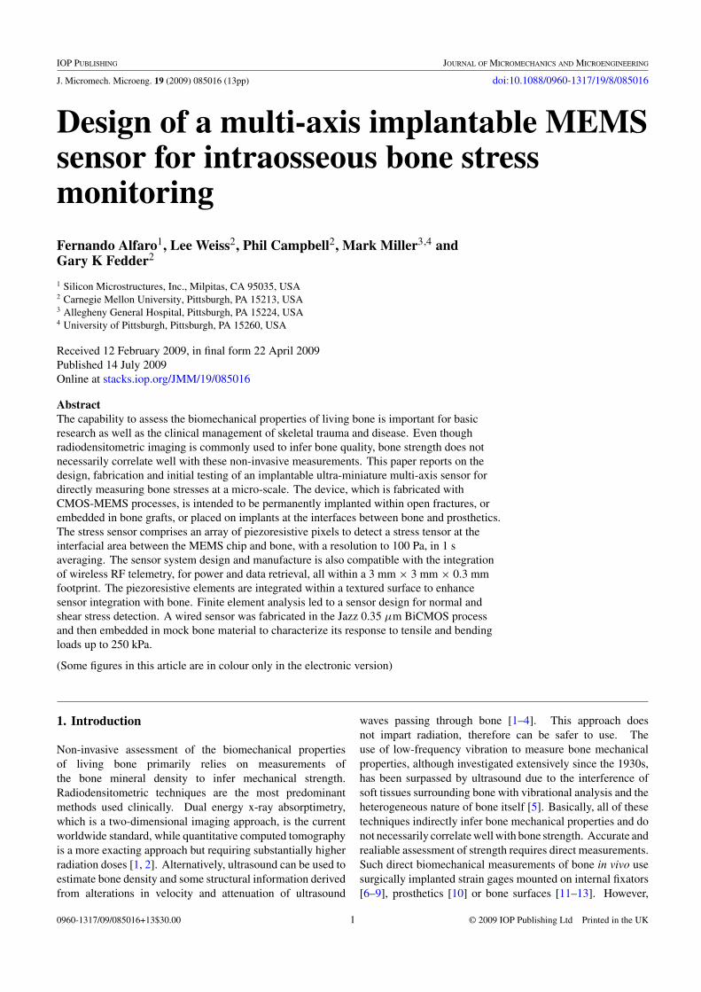
We previously proposed a wireless microminiatureintraosseous sensor system to measure multi-axis stresses atthe microscale [18]. The conceptual design of the sensor,depicted in figure 1, includes a central MEMS transducerarray, a surrounding coil antenna for wireless operation, andelectronics, all integrated on a single 3 mm × 3 mm CMOSchip. The transducer array, which has a 1 mm × 1 mmfootprint, is an 8 × 8 array of piezoresistive strain gages thatproduce the raw data needed to extract a stress tensor.
Wireless operation of the device is outside the scope of thispaper, however, it is necessary to discuss some practical issues.This work proposes a radio frequency (RF) system, basedon inductive coupling, to transfer power to and communicatewirelessly with the stress sensor. The envisioned electronicsinclude an analog RF interface, tuning capacitor, RF-to-dcrectifier system, digital control and data modulation circuits.
Silicon substrate
Stress arraywith surface texture
3 mm
0.3 mm
3 mmCoil
antenna
60 μmStress sensor in post
RFTransmitter
/Reader
External coil
θ
Figure 1. Envisioned implantable CMOS-MEMS multi-axis stresssensor.
The system would communicate with and be powered by anexternal reader/transmitter using magnetic near-field couplingthrough a resonant tuned circuit. The resonant frequencyis 13.56 MHz. While a much lower frequency can provideless signal attenuation (due to body fluid) over distance, thetransponder coil has to be physically larger. On the otherhand, a much higher frequency than 13.56 MHz enablesuse of a smaller receiving coil but suffers from more signalattenuation through tissue. Thus, resonating at 13.56 MHzprovides a good compromise for this system. For a 3 mmcoil antenna with 27 turns, a 21.8 pF capacitor is required.This is equivalent to capacitor size of 148 μm × 148 μmusing a metal–insulator–metal capacitor (1 fF μm−2) generallyavailable in RF CMOS technologies. The overall systemsize will be 3 mm × 3 mm × 0.3 mm, which should haveminimum impact on the overall strength of healed bone inwhich it is embedded. The economies of scale of CMOS-MEMS manufacturing technologies also will keep costs low,and therefore help make these sensors a practical tool forroutine clinical application.
In order to measure transmitted or residual loads, it willbe important for the transducer to become well integratedwith the surrounding bone. The incorporation of surfacetopography can enhance cell growth and osteointegration [19].In addition, coating the silicon with titanium further enhancesosteoconductivity and biocompatibility [20, 21]. Thereforebefore proceeding with detailed design of the transducer, weevaluated adult mesenchymal stem cell (hAMSC) and MG-63cell attachment and differentiation responses in vitro to severalsurface topologies on prototype of silicon chips fabricated withdeep reactive ion etching (DRIE) and coated with titanium[18]. Using these studies we determined that arrays of60 μm square posts that are 60 μm tall and spaced 60 μmapart provided satisfactory results (see figure 2 for an example)[22]. Therefore, the transducer array in figure 1 comprisessuch posts, and the top of each post incorporates a bridge offour piezoresistive stress-sensing elements and electronics formultiplexer addressing.
After the sensor has been surgically implanted, the systemsensor could be used to monitor bone healing in one of twoways. External loads could be applied to the bone duringfollow-up studies or clinical examinations. We hypothesizethat the measured load transmitted into and measured by thesensor will increase as the bone heals around the sensor. We
2

J. Micromech. Microeng. 19 (2009) 085016 F Alfaro et al
100μm
250μm 400μm
100μm
(b)
(c) (d )
(a)
50μm
Figure 2. (a) SEM of prototype titanium-coated silicon chip withtextured surface composed of 60 μm posts. (b) Live/deadfluorescent staining. Green = alive, red = dead. (c) SEMcharacterization of with MG-63 cells. (d) Si sensor topographyunderneath layer of hAMSC [22].
also speculate that measured stresses in the quiescent state (noloads applied) will correlate with bone regeneration due toresidual stresses of remodeling.
This paper reports on the next stage of sensordevelopment, including the design, fabrication and testing ofthe transducer array. A mathematical model is developed todescribe the transducer’s characteristics as a function of theorientation of applied stress and verified through finite elementanalysis. The array is fabricated in the BiCMOS process, andthen a wired version is tested by embedding it in mock bonematerial. The design and fabrication of this transducer iscompatible with its integration with an RF coil and electronicson a single chip, as will be described at the end of this paper.
2. Transducer design
2.1. Strain gage design
The analysis for the design of the piezoresistive-based sensorarray includes evaluating the sensor’s dynamic range andresolution in relation to multiple design parameters, includingresistor doping type (p- or n-), layout geometry, orientationwith respect to the crystal silicon and location on the die.Figure 3(a) shows an example of a single silicon post withpiezoresistive elements located in the silicon under the oxidelayer. The piezoresistors are arranged in a Wheatstone bridgeconfiguration, shown in figure 3(b), and signals are routedwith the interconnect stack through the suspended metal/oxidebeams. The design goals to be achieved are based on thefollowing assumptions. When the sensor is being used bya physician to evaluate bone healing, we anticipate that thephysician will apply an external pressure of around 10 kPa.Then, assuming that a 1% resolution in stress is desired, therequired minimum detectable stress for the sensor is 100 Pa.With the additional assumption that a signal-to-noise ratio(SNR) of 10 dB is acceptable, a 32 Pa equivalent input noiseis required for each piezoresistive stress sensor in the array.The maximum load that a bone can sustain is in the order ofhundreds of kPa at its upper limit. For a conservative design,this application considers a maximum load of 200 kPa.
(a) (b)
Figure 3. (a) Visualization of a 60 μm by 60 μm by 60 μm tallsilicon post indicating the location of piezoresistors in the siliconunder the oxide layer. The interconnecting beam consists of metaland oxide layers. (b) Schematic of piezoresistive Wheatstone bridge.
x , 1y , 2
z , 3
d1
y0
y1
d2
10 kPa
SYMM
SYMM
10 kPa
x , 1y , 2
z , 3KP-1KP-2
KP-4
KP-3
(a) (b)
Figure 4. One-quarter symmetric model of a bone stress sensor.
Table 1. Material properties used in FEA.
Young modulus, Poisson Density,Material E (GPa) ratio, ν ρ (kg m−3)
Cortical bone 18 0.39 2000Silicon 169 0.3 2330Beam 60 0.17 2200
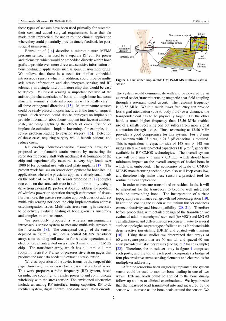
2.1.1. Finite element analysis. To aid design, finite elementanalysis (FEA) using ANSYS was used to model a prototypesensor array chip, which is shown in figure 4(a) as a one-quarter symmetric model consisting of a silicon substrate,silicon posts and oxide beams enclosed in a cube of corticalbone (not shown) that extends 1.5 mm around the chip. Thesimplified prototype did not include the coil from figure 1and is reduced in size to fit an 8 × 8 array of the 60 μmsquare posts. The material properties for the FEA solidmodel are summarized in table 1. To emulate externalstimuli, the external faces of the bone are subjected to aset of axial or shear loads along the global axes {x, y, z}.For example, a tensile stress applied to opposite faces of thebone along the x-axis corresponds to stress σxx . The chip’slocal axes {1, 2, 3} are aligned with the {x, y, z} axes. Thesuspended beams that span between posts are fabricated as partof the CMOS interconnect stack and contain silicon oxide,aluminum/titanium interconnects. The beams are modeledwith effective mechanical properties. The silicon mechanicsis approximated with a single Young’s modulus.
The FEA simulations guide placement of thepiezoresistive elements to maximize sensitivity. As oneexample simulation, a tensile load of 10 kPa is applied toopposite panels of the bone, normal to the x-axis (σxx).Symmetry conditions were applied to the interior areas of
3
J. Micromech. Microeng. 19 (2009) 085016 F Alfaro et al
d2y0 y1
[MPa]
Post Post
σ1
σ2
σ3
τ4
τ5
τ6
Figure 5. Stress components along sample line d2 in figure 4 due to10 kPa tensile stress applied along the x-axis.
the quarter model. Four keypoints were selected to setdisplacements equal to zero at anchor points. For a tensileload applied in the x-direction, the following keypoints (KP)were defined as shown in figure 4(b): KP-1 located on the yzplane has a displacement uz = 0; KP-2 in the xz plane wasset to displacement ux = 0; KP-3 and KP-4 in the xy planewas set to displacement uy = 0. Figure 5 shows the resultingstress components across the bone, posts and beam. The σ 1
component shows a higher stress at the surface of the posts withtwo peaks near the sides of the post, but lower values within thebeam that spans the two posts. This provides insight that thepiezoresistive elements should be placed on the posts, and notin the beams, to achieve a higher sensitivity. The other normalstress components (σ 2, σ 3) and shear stress components alongthe 1, 2 and 3 planes (τ 4, τ 5 and τ 6, respectively) are muchsmaller than the σ 1 component. Similar simulations wereperformed applying tensile stress along the y- and z-axes (σyy ,σ zz), and shear stresses (τ yz, τ zx , τ xy) on the side panels ofthe bone.
2.1.2. Piezoresistive stress detection. The piezoresistancechange for a two terminal piezoresistor is
�R
R= π ′
11σ1 + π ′12σ2 + π ′
13σ3 + π ′14τ4 + π ′
15τ5 + π ′16τ6, (1)
where π ′ij are the piezoresistive coefficients, which are
dependent on crystal orientation. FEA provides the tensileor shear stress values to calculate (1). The [1 0 0] directionfor n-type piezoresistors and [1 1 0] direction for p-type arechosen since these orientations provide the maximum stresssensitivity due to piezoresistive coefficients being larger inthese directions.
The piezoresistance change also depends on the locationof the piezoresistors with respect to the die and posts. This
x , 1
y , 2
z , 3
AB
C
E
F
GH
I
J
D
N
M
1 2
1
2
1 2
1 2
1 2
1
2
1
2
1
2
Post 2 ,2)
[110]
[100]
(
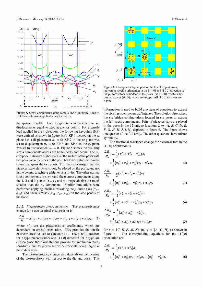
Figure 6. One-quarter layout plan of the 8 × 8 Si post array,indicating specific orientation in the [1 1 0] and [1 0 0] direction ofthe piezoresistors embedded in the posts. All [1 1 0] resistors arep-type, except {B, D}, which are n-type. All [1 0 0] resistors aren-type.
information is used to build a system of equations to extractthe six stress components of interest. The solution determinesthe six bridge configurations located in six posts to extractthe full stress components. Pairs of piezoresistors are placedin the posts in the 12 unique locations L = {A, B, C, D, E,F, G, H, M, J, I, N} depicted in figure 6. The figure showsone quarter of the full array. The other quadrants have mirrorsymmetry.
The fractional resistance change for piezoresistors in the[1 1 0] orientation is
�Rx
Rx
= 1
2
(π
p
11 + πp
12 − πp
44
)σ1
+1
2
(π
p
11 + πp
12 + πp
44
)σ2 + π
p
12σ3 (2)
�Ry
Ry
= 1
2
(π
p
11 + πp
12 + πp
44
)σ1
+1
2
(π
p
11 + πp
12 − πp
44
)σ2 + π
p
12σ3 (3)
�RB
RB
= 1
2
(πn
11 + πn12 + πn
44
)σ1
+1
2
(πn
11 + πn12 − πn
44
)σ2 + πn
12σ3 (4)
�RD
RD
= 1
2
(πn
11 + πn12 − πn
44
)σ1
+1
2
(πn
11 + πn12 + πn
44
)σ2 + πn
12σ3 (5)
for x = {C, E, F, M, N} and y = {A, G, H} as shown infigure 6. The corresponding equations for the [1 0 0]orientation are
�RI
RI
= 1
2
(πn
11 + πn12
)σ1
+1
2
(πn
11 + πn12
)σ2 + πn
12σ3 +(πn
11 − πn12
)τ6 (6)
4

J. Micromech. Microeng. 19 (2009) 085016 F Alfaro et al
RB1 RA2
RA1 RB2
VDD
V1+ -
Figure 7. Piezoresistive arrangement for Wheatstone bridge a.
�RJ
RJ
= 1
2
(πn
11 + πn12
)σ1
+1
2
(πn
11 + πn12
)σ2 + πn
12σ3 − (πn
11 − πn12
)τ6 (7)
Simplifying (1) for a {1 0 0} silicon wafer shows that theresistance of a single element is dependent on the mechanicalnormal stress components σ 1, σ 2 and σ 3, and xy shear stresscomponent τ 6. A single resistor element is not capable ofextracting an individual stress component due to the four stresscomponent dependency. However, a rosette configurationbased on two orientations and two material doping typesallows the extraction of the four stress components (σ 1, σ 2,σ 3 and τ 6). The main drawback of the rosette configurationis the dependency on temperature variations. In contrast, apiezoresistive bridge within a single post is only sensitive tothe normal stress components σ 1 and σ 2, since these stressesare uniform in such a small region. This can be demonstratedwith (2)–(7) for either doping of piezoresistors.
2.1.3. Stress tensor derivation. The piezoresistors arearranged in a set of six Wheatstone bridge configurations,labeled {a, b, c, d, e, f }, in order to cancel common modeinfluences, particularly temperature. From the structuralanalysis in the previous section, it is possible to designpiezoresistance elements within a bridge to maximize asingle component of the stress sensor based on doping type,orientation, location and geometry. As an example, the bridgea arrangement is indicated by figure 7, using the four resistorsfrom locations A and B. Similar arrangements for the otherbridges are made with the mappings: b from {C, D}, c from{M, N}, d from {E, F}, e from {G, H} and f from {I, J}.
The magnitude of the internal stress components will beaffected not only by the geometry of the transducer, but alsowith the location L on the silicon chip. For instance, regionsclose to the edges of the chip present a higher stress couplingthan center regions. The stress components σ i and τ j withinthe silicon chip are related to the external loads applied to thebone σmn, where σmn = [σxx , σyy , σ zz, τ yz, τ xz, τ xy] by
σi =∑m
∑n
Lmni σmn; i = 1, 2, 3
τj =∑m
∑n
Lmnj σmn; j = 4, 5, 6,
(8)
where Lmni represents a scaling factor coefficient of i with
respect to mn that depends on the location L where the stresscomponent is extracted from the silicon chip.
~27kPa
x , 1
y , 2
z , 3
[MPa]
~14kPa
silicon
Figure 8. Contour plot of σ 1 stress component due to 10 kPa tensileload on the x-axis. The cross section is taken at the top of the siliconin the post.
Figure 8 shows simulation results for a 10 kPa tensile loadσxx applied on the surface of the bone volume. The contourplot of the σ 1 stress component on the surface of the siliconchip illustrates the stress coupling to the external load. Amaximum stress of 26 kPa results at the posts near the edgeof the chip, whereas the stress is 14 kPa at posts in the middleregion of the chip. Similar plots were created for the differentinternal stress components, for each individual external loadapplied on the bone. The collected simulation data were usedto extract the different scaling factor coefficients Lmn
i for thesilicon chip.
The piezoresistance change as a function of external loadsis determined by substituting (8) into (2). For the bridge awith p-type piezoresistors oriented in the [1 1 0] direction inlocations (A, B), the output voltage is
Va = 1/4{(�RA1/RA1 + �RA2/RA2)
− (�RB1/RB1 + �RB2/RB2)}Vs (9)
Similar equations can be derived for the other bridges. Anumeric solution to the voltage outputs in the form of [V] =[K] · [σ ], shown in (10), was obtained by substituting thepiezoresistive coefficients and the full set of scaling factorcoefficients. In (10), [V] is in units of μV and [σ ] is in kPa.As desired in the design, bridge a has the highest sensitivityto σxx , bridge b has highest sensitivity to σyy and so on forall six bridges. By inverting [K], it is possible to extract thefull stress components from measurements of the six bridgeconfigurations located in the six posts. However, bridge ahas large cross-axis coupling (more than 14% relative to σxx)to σyy , σ zz and τ xz; bridge b has large coupling to σxx , σ zz
and τ yz; and bridge c has large coupling to σxx and σyy .The bridges d, e and f have small cross-axis coupling. Thecondition number for [K] is 6.86, which is relatively large andtranslates into an error sensitivity for stress extraction using[K]−1 of no worse than 7% of the error in the measured bridge
5
J. Micromech. Microeng. 19 (2009) 085016 F Alfaro et al
Row
add
ress
ing
Off - chip amplifier
Column addressingpixelcellVDD
C0 C1 C2
R0R1R2
n0
n1
n2
m1m0 m2
Figure 9. Basic CMOS array architecture.
voltages due to a 1% error in the input.⎡⎢⎢⎢⎢⎢⎢⎣
Va
Vb
Vc
Vd
Ve
Vf
⎤⎥⎥⎥⎥⎥⎥⎦
=
⎡⎢⎢⎢⎢⎢⎢⎣
−0.807 0.217 −0.274 0.081 −0.299 0.0050.217 −0.807 −0.262 −0.299 0.081 0.004
−0.064 −0.136 0.290 −0.011 0.029 −0.0110.049 −0.148 0.058 −1.144 −0.011 −0.052
−0.148 0.049 0.062 −0.011 −1.144 −0.017−0.016 −0.016 0.026 0.024 0.024 1.938
⎤⎥⎥⎥⎥⎥⎥⎦
·
⎡⎢⎢⎢⎢⎢⎢⎣
σxx
σyy
σzz
τyz
τxz
τxy
⎤⎥⎥⎥⎥⎥⎥⎦
(10)
3. Circuit design and implementation
3.1. Topology
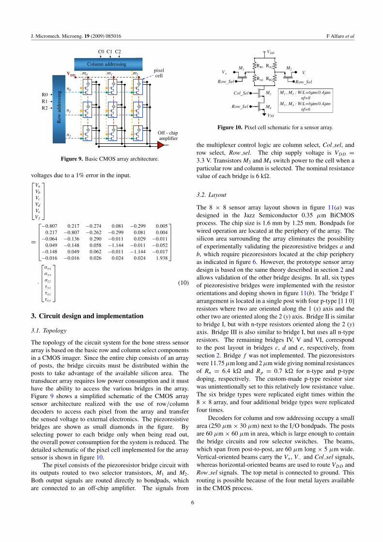
The topology of the circuit system for the bone stress sensorarray is based on the basic row and column select componentsin a CMOS imager. Since the entire chip consists of an arrayof posts, the bridge circuits must be distributed within theposts to take advantage of the available silicon area. Thetransducer array requires low power consumption and it musthave the ability to access the various bridges in the array.Figure 9 shows a simplified schematic of the CMOS arraysensor architecture realized with the use of row/columndecoders to access each pixel from the array and transferthe sensed voltage to external electronics. The piezoresistivebridges are shown as small diamonds in the figure. Byselecting power to each bridge only when being read out,the overall power consumption for the system is reduced. Thedetailed schematic of the pixel cell implemented for the arraysensor is shown in figure 10.
The pixel consists of the piezoresistor bridge circuit withits outputs routed to two selector transistors, M1 and M2.Both output signals are routed directly to bondpads, whichare connected to an off-chip amplifier. The signals from
V+ V-
VDD
Vss
M1 M2
M3
M4
Col_Sel
Row_Sel
Row_Sel
Row_Sel
RB1
RA1
RA2
RB2
M1 , M2 : W/L=6μm/0.4μmnf=8
M3 , M4 : W/L=6μm/0.4μmnf=6
Figure 10. Pixel cell schematic for a sensor array.
the multiplexer control logic are column select, Col sel, androw select, Row sel. The chip supply voltage is VDD =3.3 V. Transistors M3 and M4 switch power to the cell when aparticular row and column is selected. The nominal resistancevalue of each bridge is 6 k�.
3.2. Layout
The 8 × 8 sensor array layout shown in figure 11(a) wasdesigned in the Jazz Semiconductor 0.35 μm BiCMOSprocess. The chip size is 1.6 mm by 1.25 mm. Bondpads forwired operation are located at the periphery of the array. Thesilicon area surrounding the array eliminates the possibilityof experimentally validating the piezoresistive bridges a andb, which require piezoresistors located at the chip peripheryas indicated in figure 6. However, the prototype sensor arraydesign is based on the same theory described in section 2 andallows validation of the other bridge designs. In all, six typesof piezoresistive bridges were implemented with the resistororientations and doping shown in figure 11(b). The ‘bridge I’arrangement is located in a single post with four p-type [1 1 0]resistors where two are oriented along the 1 (x) axis and theother two are oriented along the 2 (y) axis. Bridge II is similarto bridge I, but with n-type resistors oriented along the 2 (y)axis. Bridge III is also similar to bridge I, but uses all n-typeresistors. The remaining bridges IV, V and VI, correspondto the post layout in bridges c, d and e, respectively, fromsection 2. Bridge f was not implemented. The piezoresistorswere 11.75 μm long and 2 μm wide giving nominal resistancesof Rn = 6.4 k� and Rp = 0.7 k� for n-type and p-typedoping, respectively. The custom-made p-type resistor sizewas unintentionally set to this relatively low resistance value.The six bridge types were replicated eight times within the8 × 8 array, and four additional bridge types were replicatedfour times.
Decoders for column and row addressing occupy a smallarea (250 μm × 30 μm) next to the I/O bondpads. The postsare 60 μm × 60 μm in area, which is large enough to containthe bridge circuits and row selector switches. The beams,which span from post-to-post, are 60 μm long × 5 μm wide.Vertical-oriented beams carry the V+, V− and Col sel signals,whereas horizontal-oriented beams are used to route VDD andRow sel signals. The top metal is connected to ground. Thisrouting is possible because of the four metal layers availablein the CMOS process.
6

J. Micromech. Microeng. 19 (2009) 085016 F Alfaro et al
Power supply clamp
I/O pads
C0
C1
C2
V-
V+
Vdd
Vss
R0
R1
R2
Decoder
Column switches
Testresistors
8x8 array
1.6 mm
1.25 mm
post
ESD diodes
m0 m1 m2
n0
n1
Bridge IIIBridge I
Bridge VIBridge VBridge IV
Bridge II
V+
V-
Col_sel
VDD
VSS
Row_sel
p-typeresistors
Switches
n-typeresistors
(a) (b)
Figure 11. Layout view of the 8 × 8 array bone stress sensor. (a) Full layout of the 1.6 mm × 1.25 mm sensor chip. (b) Layout detail ofsensor elements.
Electronics Resistor
(a)
n-well
Scalable CMOS Diffused Resistor Silicon Substrate
Oxide Metal interconnect
(b) (c)
Silicon Substrate Silicon Substrate
(d ) (e)
Figure 12. Layout view and cross section of the post-CMOS process. (a) Layout view of two posts. (b) CMOS chip from foundry.(c) Oxide etch. (d) DRIE. (e) Isotropic etch.
4. Prototype device fabrication
4.1. MEMS post-CMOS processing
After completion of the foundry CMOS processing, a MEMSprocess was used for the microfabrication of the sensor posts.The process is based on prior work in our group to fabricatemicrostructures with high-aspect-ratio (about 5:1) composite-beam suspensions by using conventional CMOS processingfollowed by a sequence of maskless dry-etching steps[23, 24]. Figure 12 summarizes the post-CMOS MEMSfabrication steps. The CMOS chip received from thefoundry consists of a silicon substrate with a thicknessof approximately 350 μm. The first step is an oxidereactive-ion etch (RIE) with a PlasmaTherm 790 system.The oxide etch time is approximately 5 h to etch throughthe 9 μm thick dielectric stack. The gases used areCHF3 (22.5 sccm) and O2 (16 sccm), with a pressure of100 mT and a power setting of 100 W. Once the siliconsubstrate is exposed, the chip is transferred to a SurfaceTechnology System inductively coupled plasma reactor to
perform a timed deep Si RIE step to a trench depth of60 μm. The final process step is a short Si isotropic etchto undercut and release the 5 μm wide beams.
Electronics in the posts were placed at least 10 μm fromthe Si trench edge to prevent failure of circuits because ofSi micromachined undercut. Figure 13 shows SEMs of thereleased sensor array chip. The total etch depth is 60 μm, andthe undercut of the posts is approximately 3 μm. This undercutwas not included in the stress simulation of the 60 μm ×60 μm posts due to meshing limitations of our ANSYS license.The undercut might increase the stress value estimation as itis shown in section 5.
4.2. Embedding device in tensile testing specimen
Mechanical characterization of the sensor array, as describedin the following section, was performed by first mountingit to a custom printed circuit board (PCB), to provideaccess to external wiring, embedding the array/PCB ina ‘dog-bone’ ASTM standard test specimen (shown infigure 14(a)), and then subjecting the completed test specimen
7

J. Micromech. Microeng. 19 (2009) 085016 F Alfaro et al
(a) (b)
Figure 13. SEMs of the bone stress sensor after micromachining the 0.35 μm BiCMOS chip. (a) Released 8 × 8 sensor array. (b) Detail ofposts with rounded corners.
Resin
PCBSensor
Resin
PCB Sensor
(a) (b)
Figure 14. ASTM D 638 specimen with embedded chip.
to controlled stresses. The PCB was thinned down to 300 μmto decrease its stiffness and minimize its overall effect on thespecimen’s mechanical properties. A Batwing 22 lead framefrom standard Surface Mount Technology packages [25] wasbonded to the PCB, and then the CMOS chip was bonded tothe lead frame using a silver conductive epoxy based adhesive(CW2400 CircuitWorks R©, ITW Chemtronics”). Connectionsfrom the chip pads were then wire bonded to the lead frame asshown in figure 14(b).
The material for the dog-bone specimen was Veriflex R©
resin [26], which has a compressive modulus of 1.465 GPa,similar to cancellous bone, and which also has temperature-dependent elastic properties to be able to simulate differentbone stiffnesses. The resin solution was first mixed and placedin a vacuum desiccator to remove air bubbles. The solution wasthen poured to a thickness of 0.12′′ into a 3′′ × 5′′ rectangularmold made with glass sheets. The sample was cured in anoven at 75 ◦C for 36 h. The PCB was then bonded to thisresin sheet using an epoxy-based adhesive (#4001, extra-fastsetting epoxy, Hardman). More resin was then poured overand cured on the top of the first sheet to enclose the chip.After curing and release, the two layer resin structure wascut into a dog-bone test specimen according to ASTM D638[27].
Possible mechanical failure modes of the sensor mostlikely will occur at the 9.63 μm wide by 5.3 μm tall by60 μm long CMOS-MEMS suspended beams interconnecting
the silicon posts rather than within the silicon posts, which aremuch larger. Failure from stress could originate from axialstress or by in-plane shear stress. However, no failure wasobserved in any of the embedded tests that were performed.Furthermore, a destructive test was performed to verifythe mechanical properties of the resin and no fracture ordelamination was observed in the sensor. In this test, aspecimen was subject to a tensile load in a MTS Bionix 858load test system at a rate of 2 mm in 2 min. The maximumload at failure was 1.2 kN.
The oxide-metal beams that span from post to postare estimated to have a fracture strain greater than 1%,corresponding to a normal stress of greater than 600 kPa andlarger than the intended applied loads. We believe the 1%strain estimate is conservative, since the axial stress fracturelimit of silicon dioxide fibers is listed as 8.4 GPa [28].
In the case of shear failure, for a typical stress of 10 kPaapplied to the arm the corresponding shear stress on the Si postsis only 0.8 kPa, and 4–5 kPa at the beams and posts corners.The shear fracture stress of 53 μm thick oxide microstructurering membranes has been measured at 3–5 MPa [29]. Thestrength of a given structure depends greatly on the shape andpresence of any defects, especially sharp corners. The currentdesign of the bone stress sensor includes round corners at Siposts and chamfered intersections at the end of suspendedbeams for stress relief.
8

J. Micromech. Microeng. 19 (2009) 085016 F Alfaro et al
TPR = 2 ms
2000 pts
[mV
olts
]
n = 1
Time [seconds]
n = 2 n = 128
Sample1 = SUM(AVGs mV )/128
AVG(1)=SUM(data mV)/2000
0.256s
Figure 15. Oscilloscope configuration for LabView data capture.
5. Experimental results
5.1. Tensile testing
A custom-made tensile test rig was built consisting of a fixedgripper clamped to the top part of the dog-bone specimen anda free clamp at the other end where calibrated weights wereapplied (100–500 gm). Data were recorded with NationalInstruments (NI) LabVIEW software. A NI-USB-6009 dataacquisition unit was connected through the computer USBport. Six data lines (bits) were used to activate the row decoder(3 bits) and the column decoder (3 bits), in order to accessthe 8 × 8 sensor array. The sensor’s differential output wasconnected to an off-chip precision instrumentation amplifier(Analog Devices AD624) with a voltage gain of 200. TheAD624 is a high precision, low noise (0.2 μVpp, 0.1 to 10 Hz)instrumentation amplifier designed primarily for use with lowlevel transducers. The AD624C has an input offset voltagedrift of less than 0.25 μV ◦C−1, output offset voltage driftof less than 10 μV ◦C−1, CMRR above 80 dB at unity gain(130 dB at G = 500), and a maximum nonlinearity of 0.001%at G = 1. A NI GPIB USB-B controller sampled data from anAgilent 54622A oscilloscope by averaging 2000 data points ina 2 ms time per record (TPR) as shown in figure 15. A total of128 records were collected and later averaged in software. Thecorresponding total averaging time for one measured samplewith this configuration was 256 ms (2 ms × 128 records).
Figure 16 shows the output of several type III bridgeslocated at the sixth column of the 8 × 8 array bone stresssensor prototype. This type of bridge is sensitive to tensile orcompressive stress. The total averaging time for five sampleswas 1.28 s for all data. The measured standard deviation forthis data set at the output of the off-chip amplifier was 226 μV.Assuming a 10 dB SNR, the minimum detectable signal withinthe mock bone/PCB assembly is 23.8 kPa (2.38 N). This valueis much higher than the desired resolution since most of theload is transferred to the PCB since, although the PCB is thin,it is made of a much stiffer material than the mock bone andthus shunts a significant amount of stress.
The initial measurements demonstrate the basicfunctionality of the stress sensor to detect normal stress.However, to better characterize the device it will be necessaryto avoid the hardwired test approach requiring a PCB. Thisissue will be addressed in the next version of sensor designby using an on-chip wireless system. In addition, an on-chipamplifier would increase the output signal and reduce some
0
2
4
6
8
0 10 20 30 40 50
ΔV
out [
mV
]
Load [N]
III-1
III-2
III-3
III-4
Simulation
III-type bridges
Figure 16. Output for type III bridges in tension.
0
0.75
1.5
2.25
3
0 10 20 30 40
ΔV
out [
mV
]Load [N]
VI-1
VI-2
VI-3
VI-4
Simulation
VI-type bridges
Figure 17. Output for type VI bridges in tension.
of the noise originated by the wiring from the PCB to thetesting instruments. Also, without the PCB, the test specimenpreparation will be simplified, and reduce the bubble formationdue to air trapped between the PCB and the first resin layer. Areference gage could also be attached during the test specimenpreparation to verify the axial loads during tensile or bendingtests.
The applied test loads correspond to a stress range from30 kPa to 400 kPa. The stress sensitivity prior to amplificationis 190 μV V−1 MPa−1. The output change follows the trend ofthe simulation data shown in figure 16. The nonlinearity in thebridge’s voltage output is believed to be due to non-uniformityin the resin around the device. Figure 17 shows the output ofseveral type IV bridges located at the sixth column of the8 × 8 sensor array. These pixels are sensitive to shearstress. While these sensor bridges have highly nonlinear outputwith tensile load, their measured sensitivity to axial stress issmall, as desired. Further experimental assessment of thisbridge design to validate its utility in shear stress detection isneeded.
5.2. Bend testing
A four-point bending test rig was built to measure the behaviorof the sensor under compressive and tensile loads. Figure 18shows a schematic of the bending test rig, which is based ona G22G flexure fixture. Two forces act on the upper sideof the specimen, with a span of L/3, where L refers to themajor span between the bottom supports. Figure 19 showsthe cross section of a simply supported loaded beam, with amagnified bending caused by the load. The applied load to thebeam and the support force generate internal shearing forcesand internal torque called bending moments. For clarity, the
9

J. Micromech. Microeng. 19 (2009) 085016 F Alfaro et al
L/3 /3 L/3L
Figure 18. Schematic and model of a 4-point bend test fixture.
second diagram does not show vertical shear force, but showshorizontal forces (−Fx and +Fx). As the beam bends, the topregion of the beam is put into compression and the bottomregion of the beam is put into tension. This results in internalaxial forces (horizontal, x-axis) acting in the beam. The chipis located approximately 1.5 mm with respect to the axialcenterline of the beam.
Figure 20 shows the output of replicate [1 1 0] n-typebridges located in column 2 during bending in tension, whereasfigure 21 shows the output during bending in compression.When the specimen (figure 14) is placed in the test fixture(figure 18) in the normal orientation, the sensor is above theaxial centerline of the beam. In this case, the top region is putinto compression. During tension, the test specimen is flippedupside down, and the sensor experiences a tensile force. Theobserved standard deviation for this data set at the output of theoff-chip amplifier was 160 μV. For a 10 dB SNR, the minimumdetectable signal is 18 kPa.
All of the 64 bridges were tested under bending stressand all were functional. As expected from the analysis insection 2, the bridges closer to the edge have a higher output.
5.3. Temperature characterization
The bridge circuit eliminates common-mode changes in theoutputs of the stress sensors due to temperature variationsand drift. However, the rest of the electronics, including theswitches to power each pixel, the decoders and the electrostaticdischarge protection were not designed to be immune totemperature changes. A circuit simulation was performedto quantify bridge current as a function of temperature, and
Load
Support force
M
V -Fx
+Fx
+Fx
-Fx
M
(a) (b)
Figure 19. Resultant forces and moments due to beam bending. (a) Beam section showing shear force and bending moment. (b) Axialforces due to beam bending.
0
2
4
6
8
10
12
0 10 20 30 40 50
ΔV
out [
mV
]
Load [N]
III-1
III-2
III-3
III-4
Simulation
III-type bridges
Figure 20. Output for type III bridges during bending in tension.
0
2
4
6
8
10
12
0 10 20 30 40 50-Δ
Vou
t [m
V]
-Load [N]
III-1
III-2
III-3
III-4
Simulation
III-type bridges
Figure 21. Output for type III bridges during bending incompression.
the results were compared to experimental data. A releasedchip was wirebonded to a metal lead frame on a thinned PCB.The sensor and PCB were placed inside an oven to record thebridge current, I, across a temperature range from 20 ◦C to75 ◦C, with data for two bridges shown in figure 22. Thetemperature sensitivity of the measured current matches thatobtained through simulation. The offset in the plot is due tothe difference between the nominal and actual value R0 forthe designed resistors. The simulation uses 6.4 k� resistorsand the actual resistor values were within 7% of the designedvalue. There is also an offset between the [1 1 0] and the[1 0 0] resistors, since the latter were made with custom layoutby rotating the resistors by 45◦ using a Manhattan stairstepapproximation. The power consumed by each bridge during ameasurement cycle is a maximum of 775 μW (3.3 V supply).The total energy expended for sequential activation of sixbridges is 1.2 mJ. The power could be lowered by loweringthe supply voltage. Larger values of piezoresistors would also
10

J. Micromech. Microeng. 19 (2009) 085016 F Alfaro et al
190
210
230
250
20 40 60 80
Iin
[μA
]
Temperature [Celsius]
Simulation
VI-type bridge
III-type bridge
Figure 22. Current Iin for two III-type and VI-type bridges as afunction of temperature.
-160
-140
-120
-100
-80
1.E+02 1.E+03 1.E+04 1.E+05
dB
V/H
z
[Hz]
Noise Floor
Sensor + Amp
Amp
Figure 23. Measured output referred noise.
lower power, however their size is constrained by the availablesilicon post area. Average power would be greatly reduced byrunning the sensor at a low duty cycle, for example once everyfew seconds. In wireless power operation, a capacitor to storethe scavenged energy would be required to drive the bridge atits duty cycle.
5.4. Noise analysis
The piezoresistors forming the stress sensors, have inherentnoise voltage
√υ2
n,res =√
4kBT R�f (11)
where T is the temperature in Kelvin, kB is Boltzmann’sconstant 1.38 × 10⁻²³ m2 kg s−2 K−1, R is the resistance and�f is the circuit bandwidth in Hz. A 6455 � resistive bridgein a 1 Hz bandwidth will add noise of 10.3 nV Hz−1/2. Theoff-chip amplifier has an input referred noise of 4 nV Hz−1/2.Adding the noise power together yields a total theoretical noiselevel of 11.1 nV Hz−1/2. The measured output referred noiseof the amplifier and of the total sensor/amplifier system isshown in figure 23. The total measured input referred noisewas 17.6 nV Hz−1/2, which was well above the spectrumanalyzer noise floor and close to the calculated value. For aminimum in-plane shear stress of 100 Pa, the expected outputvoltage from the bridge is 0.2 μV. Using the 17.6 nV Hz−1/2
noise voltage in the 256 ms averaging time the respective SNRis 15.2 dB. Thus, the intrinsic noise of the sensor is sufficientfor the bone stress monitoring application.
0
2
4
6
8
0 10 20 30 40 50
ΔV
out [
mV
]
Load [N]
III-1, UnloadIII-2, UnloadIII-1, LoadIII-2, Load
III-type bridges
Figure 24. Hysteresis behavior in a four-point bending fixture forIII-type bridges.
5.5. Hysteresis
Hysteresis behavior was assessed using the bending test rigdescribed above. Figure 24 shows the output voltage changeduring loading (dashed lines) and unloading (opened markers)during bending. The overall characteristic of the sensor showsgood linearity during loading and unloading for all the pixelstested. The mean relative difference between the two sets ofvalues is lower than 10% of the full scale. These voltagedifferences are attributed to movement in the fixture and/orerror due to noise during the measurement. No noticeablehysteresis was observed during different tests.
6. Conclusions
The results presented in this paper are a first step in thedevelopment of an implantable wireless piezoresistive bonestress sensor with active electronics readout. Texturing of thesilicon CMOS chip surface into 60 μm × 60 μm × 60 μm tallposts will help to enhance cell growth and osteointegration.An initial wired prototype of the multi-axis transducer withan 8 × 8 array of silicon posts with CMOS electronics wasable to successfully measure compressive and tensile stresses.The experimental prototype provides a partial validation ofthe concept in section 2. The measured input referred noiseof 17.6 nV Hz−1/2 is sufficient for the bone stress application,however a wireless chip prototype without rigid PCB wiringis required to detect the targeted 100 Pa stress levels. Futuredesigns can ac modulate the bridge current to reduce the flickernoise.
The on-chip CMOS electronics enables the measurementof internal normal and shear stress data for all three axes.A general theoretical formulation was derived for the use ofpiezoresistive bridges within the sensor’s surface topography.By incorporating an array of six Wheatstone bridges basedon the selection of p-type and n-type piezoresistive elementsrelative to the silicon crystallographic orientation, it is possibleto determine the normal and shear stresses under a singleload in a bone-like material. In order to resolve all the stresselements, piezoresistors in at least two of the bridges must beplaced far apart on the chip, as determined through simulation.In the future, piezoresistors located in posts at the peripheryof the chip will enable full validation of the array concept insection 2 through experimental measurement and extraction of
11

J. Micromech. Microeng. 19 (2009) 085016 F Alfaro et al
all six normal and shear stress components for a given externalload. Finally, the condition number of the matrix [K] in (10)could be decreased with sensor design optimization to increaseaxial sensitivity and reduce cross-coupling. Parameters such aspiezoresistive location, shape of silicon posts or incorporationof polysilicon piezoresistors on beams can be used to improvethe current design.
Design of an on-chip coil, power conditioning electronicsand RF communication electronics on the CMOS chip ischallenging, but feasible in future work. Implantation depthsover which RF telemetry will have to be established willdepend on the specific location where the sensor will beimplanted and on the physical characteristics of the patient.Interpretation of the measured signal will require knowing theorientation of the sensor within bone. Adjusting the orientationof the external coil to maximize RF coupling should providethe required information, however this represents anothersystem design challenge.
The bone stress sensor may, in the long-term, enablein vivo experiments for a deeper understanding of bone tissuestructure and function. Its capability to measure and quantifybiomechanical properties in vivo would potentially make itan enabling technology for many applications, including asa tool to gain new knowledge about bone regeneration andremodeling at the micro-scale and aid in the development andverification of new graft materials, and, ultimately to provideimproved information in real-time for clinical management ofosteogenic diseases and trauma.
Acknowledgment
This work was supported in part by The PennsylvaniaInfrastructure Technology Alliance and The TechnologyCollaborative (former Pittsburgh Digital Greenhouse). Theauthors would also like to thank the members of theCarnegie Mellon Nanofabrication Facility for assistance withfabrication, and Duquesne University for assistance with cellexperiments.
References
[1] Gilsanz V 1998 Bone density in children: a review of theavailable techniques and indications Eur. J. Radiol.26 177–82
[2] Baroncelli G I 2008 Quantitative ultrasound methods to assesbone mineral status in children: technical characteristics,performance, and clinical application Pediatr. Res. 63 220–8
[3] Hans D and Krieg M-A 2008 The clinical use of quantitativeultrasound (QUS) in the detection and management ofosteoporosis IEEE Trans. Ultrason. Ferroelectr. Freq.Control 55 1529–38
[4] Nicholson P H F 2008 Ultrasound and biomechanicalcompetence of bone IEEE Trans. Ultrason. Ferroelectr.Freq. Control 55 1539–45
[5] Nokes L D M 1999 The use of low-frequency vibration inorthopaedics Proc. Inst. Mech. Eng. 213 271–90
[6] Bergmann G, Graichen F, Siraky J, Jendrzynski Hand Rohlmann 1988 A Multichannel strain gauge telemetryfor orthopaedic implants J. Biomech. 21 169–76
[7] Burny F et al 2000 Concept, design and fabrication of smartorthopedic implants Med. Eng. Phys. 22 469–79
[8] Elvin N, Elvin A and Spector M 2000 Implantable bone straintelemetry sensing system and method US Patent 6,034,296
[9] Webster D J, Morley P L, Lenthe G H V and Muller R 2008 Anovel in vivo mouse model for mechanically stimulatedbone adaptation—a combined experimental andcomputational validation study Comput. Methods Biomech.Biomed. Eng. 11 435–41
[10] Hsieh M C, Fang Y K, Ju M S, Chen G S, Ho J J, Yang C,Wu P M, Wu G and Chen T Y F 2001 A contact-typepiezoresistive micro-shear stress sensor for above-kneeprosthesis application J. Microelectromech. Syst. 10 121–7
[11] Hoshaw S J, Fyhrie D P, Takano Y, Burr D B and Milgrom C1997 A method suitable for in vivo measurement of bonestrain in humans J. Biomech. 30 521–4
[12] Tang W 2005 Biomechanics at the micro scale EmergingInformation Technology Conf. pp 1–5
[13] Yang G, Bailey V, Wen Y H, Lin G, Tang W and Keyak J 2004Fabrication and characterization of microscale sensors forbone surface strain measurement Proc. IEEE Sensors3 1355–8
[14] Benzel E, Kayanja M, Fleischman A and Roy S 2006 Spinebiomechanics: fundamentals and future Clin. Neurosurg.53 98–105
[15] An Y H 2000 Mechanical Testing of Bone and theBone-Implant Interface ed Y H An and R A Draughn (BocaRaton, FL: CRC Press) pp 41–64
[16] Cil A, Veillette C J, Sanchez-Sotelo J, Sperling J W, Schleck Cand Cofield R H 2009 Revision of the humeral componentfor aseptic loosening in arthroplasty of the shoulder J. BoneJoint Surg. Br. 91 75–81
[17] Melik R, Perkgoz N K, Unal E, Puttlitz C and Demir H V 2008Bio-implantable passive on-chip RF-MEMS strain sensingresonators for ortopaedic applications J. Micromech.Microeng. 18 1–9
[18] Alfaro J F, Weiss L E, Campbell P G, Miller M C, Heyward C,Doctor J S and Fedder G K 2005 Bioimplantable bone stresssensor 27th Ann. Int. Conf. of the Engineering in Medicineand Biology Society, IEEE-EMBS vol 1 pp 518–21
[19] Chehroudi B, McDonnell D and Brunette D M 1997 Theeffects of micromachined surfaces on formation of boneliketissue on subcutaneous implants as assessed by radiographyand computer image processing Biomed. Mater. Res. J.34 279–90
[20] Albrektsson T and Hansson H A 1986 An ultrastructuralcharacterization of the interface between bone and sputteredtitanium or stainless steel surfaces Biomaterials7 201–5
[21] Johansson C B, Hansson H A and Albrektsson T 1990Qualitative interfacial study between bone and tantalum,niobium or commercially pure titanium Biomaterials11 277–80
[22] Heyward C 2004 The importance of Si surface topography inthe attachment, proliferation, and differentiation of humanadult mesenchymal stem cells Masters Thesis DuquesneUniversity Pittsburgh, PA
[23] Fedder G K, Santhanam S, Reed M L, Eagle S C, Guillou D F,Lu M S-C and Carley L R 1997 Laminatedhigh-aspect-ratio microstructures in a conventional CMOSprocess Sensors Actuators A 57 103–10
[24] Xie H, Zhu X, Erdmann L, Gabriel K J and Fedder G K 2000A novel micromachining process for high-aspect-ratioCMOS-MEMS Tech. Dig. of Solid-State Sensor andActuator Workshop (Hilton Head Island, SC) vol 1pp 77–80
[25] Co-planar Inc 2006 Precision stamped metal and mylarcomponents, Denville, NJ http://www.co-planar.com/
[26] CRG Industries LLC 2006 Veriflex R© shape memory polymerresin systems, Cornerstone Research Group, Inc., Dayton,OH http://www.crgrp.net/veriflex.htm
12
J. Micromech. Microeng. 19 (2009) 085016 F Alfaro et al
[27] American Society for Testing and Materials 2003 ASTMD638-03 Standard test method for tensile properties ofplastics, Philadelphia, PA http://www.astm.org/
[28] Petersen K E 1982 Silicon as a micromechanical materialProc. IEEE 70 420–57
[29] Zhang C and Najafi K Fabrication of thick silicon dioxidelayers using DRIE, oxidation and trench refill Proc. 15thIEEE Int. Conf. on Micro Electro Mechanical Systems(MEMS ‘02) (Las Vegas, NV, January 20–24 2002)pp 160–3
13