design of a high performance silicon carbide cmos
TRANSCRIPT

University of Arkansas, FayettevilleScholarWorks@UARK
Theses and Dissertations
12-2014
Design of a High Performance Silicon CarbideCMOS Operational AmplifierShaila Amin BhuyanUniversity of Arkansas, Fayetteville
Follow this and additional works at: http://scholarworks.uark.edu/etd
Part of the Electronic Devices and Semiconductor Manufacturing Commons, and the VLSI andCircuits, Embedded and Hardware Systems Commons
This Thesis is brought to you for free and open access by ScholarWorks@UARK. It has been accepted for inclusion in Theses and Dissertations by anauthorized administrator of ScholarWorks@UARK. For more information, please contact [email protected], [email protected].
Recommended CitationBhuyan, Shaila Amin, "Design of a High Performance Silicon Carbide CMOS Operational Amplifier" (2014). Theses and Dissertations.2042.http://scholarworks.uark.edu/etd/2042
Design of a High Performance Silicon Carbide CMOS Operational Amplifier
Design of a High Performance Silicon Carbide CMOS Operational Amplifier
A thesis submitted in partial fulfillment
of the requirements for the degree of
Master of Science in Electrical Engineering
by
Shaila Amin Bhuyan
University of Dhaka
Bachelor of Science in Applied Physics, Electronics and Communication Engineering, 2012
December 2014
University of Arkansas
This thesis is approved for recommendation to the Graduate Council
Dr. H. Alan Mantooth
Thesis Director
Dr. Simon Ang
Committee Member
Dr. A. Matthew Francis
Committee Member

ABSTRACT
This thesis presents the design, simulation, layout and test results of a silicon carbide (SiC)
CMOS two-stage operational amplifier (op amp) with NMOS input stage. The circuit has been
designed to provide a stable open-loop voltage gain (60 dB), unity-gain bandwidth (around 5
MHz) and maintain a high CMRR and PSRR within a useful input common mode range over
process corners and a wide temperature range (25 °C – 300 °C). Between the two stages a Miller
compensation topology is placed to improve the phase margin (around 450). Due to the
comparatively high threshold voltage values of transistors in SiC, the power supply is maintained
at 15 V. There is a maximum of 21% variation in DC gain from 25 0C to 275
0C and the unity-
gain bandwidth and slew rate improves with higher temperature. The major application area of
this op amp is in high temperature environments where silicon (Si) integrated circuits (IC) fail to
perform. In addition, the design of a second version of the operational amplifier is covered,
which aims to provide more functionality and improved performance.

ACKNOWLEDGEMENTS
I would like to express my gratitude to Dr. H. Alan Mantooth for his guidance and
encouragement throughout the pursuit of my Master’s degree. I am thankful for the opportunity
to be part of the Mixed-Signal Computer-Aided Design group. I would also like to thank my
thesis committee members, Dr. Simon Ang and Dr. A. Matthew Francis for their valuable
participation. I would like to thank the faculty and staff of the Electrical Engineering Department
for their cooperation.
I am grateful to Dr. Francis for his support, motivation and contribution throughout my entire
time at the University of Arkansas. A special thank you to my project team members, Jim
Holmes, Ashfaqur Rahman, Paul Shepherd, Matthew Barlow, Shamim Ahmed, Dillon Kaiser
and everybody else who was involved in the project. Whenever I am faced with something new
or challenging I can always run by them for their help and suggestions. I would like to extend my
thanks to everyone involved in the NSF-BIC project at University of Arkansas, Ozark Integrated
Circuits Inc. and Raytheon Systems Limited for their support and cooperation during the project.

DEDICATION
This thesis is dedicated to my husband, Fahad Hossain, who has always been my biggest
supporter, my sisters Fahima Amin Bhuyan & Saima Amin Bhuyan for always believing in me
and most importantly to my parents Dr. Aminul Haque Bhuyan and Farida Begum for their
unconditional love and confidence in me.

TABLE OF CONTENTS
Chapter 1 .......................................................................................................................................... 1
Introduction ...................................................................................................................................... 1
1.1 Overview of Operational Amplifier ...................................................................................... 2
1.2 Applications ....................................................................................................................... 5
1.2.1 2nd order Active Low Pass Filter ................................................................................... 5
1.2.2 Digital to Analog Data Converters ................................................................................ 6
1.2.3 High-Side Current Sensing Circuit ................................................................................ 7
1.3 Silicon Carbide CMOS Technology ..................................................................................... 8
1.4 Thesis Organization ............................................................................................................ 9
Chapter 2 Operational Amplifier Topologies .................................................................................. 10
2.1 Two-Stage Miller Compensated CMOS Op Amp ................................................................ 10
2.2 Three-Stage Nested Miller Compensation CMOS Op Amp .................................................. 12
Chapter 3 CMOS Operational Amplifier Design ............................................................................. 14
3.1 Design Procedure .............................................................................................................. 14
3.2 Design Specifications ........................................................................................................ 15
3.3 Circuit Design .................................................................................................................. 16
3.3.1 Compensation Circuit ................................................................................................ 18
3.3.2 Differential Input Stage .............................................................................................. 21
3.3.3 Common-Source Output Stage ................................................................................... 25
Chapter 4 Simulation of the Operational Amplifier ......................................................................... 30
4.1 Simulation Setup .............................................................................................................. 30
4.2 DC Simulation .................................................................................................................. 31
4.3 AC Simulation .................................................................................................................. 36
4.4 Transient Simulation ......................................................................................................... 39
Chapter 5 Physical Design ............................................................................................................ 41
5.1 Chip Layout ..................................................................................................................... 41
Chapter 6 Testing and Characterization .......................................................................................... 48
6.1 Bond Wire and Packaging ................................................................................................. 48
6.2 Test Setup ........................................................................................................................ 50
6.3 Test Results ...................................................................................................................... 53
Chapter 7 Conclusion ................................................................................................................... 61
References ...................................................................................................................................... 63
Appendix – A .................................................................................................................................. 65
Op Amp Test Plan ........................................................................................................................... 65
A. General Power-up Procedure ................................................................................................. 65
B. High Temperature General Procedure .................................................................................... 66
C. DC Characterization ............................................................................................................. 66
DC Offset ................................................................................................................................ 66
DC Power ................................................................................................................................ 67
Input Common Mode Range (ICMR) Voltage Measurement ....................................................... 68
D. AC Characterization ............................................................................................................. 69
Open Loop Gain ....................................................................................................................... 69
Unity-Gain Bandwidth ............................................................................................................. 70
Common Mode Rejection Ratio (CMRR) .................................................................................. 71
Power Supply Rejection Ratio (PSRR) ...................................................................................... 72
E. Transient Characterization..................................................................................................... 73
Slew Rate ................................................................................................................................ 73
Appendix – B .................................................................................................................................. 74
Design of an Op Amp in the Subsequent Run .................................................................................... 74

LIST OF FIGURES
Fig. 1.1.1. Operational amplifier equivalent circuit [5]. ................................................................. 2
Fig. 1.1.2. Non-ideal linear characteristics of op amp [6]. ............................................................. 3
Fig. 1.2.1. 2nd
order active low pass filter [8]. ................................................................................ 6
Fig. 1.2.2. Current mode R-2R DAC [9]. ....................................................................................... 7
Fig. 1.2.3. Current sensor with single op amp difference amplifier [10]. ....................................... 8
Fig. 1.3.1. SiC CMOS process architecture. ................................................................................... 9
Fig. 2.1.1. Block diagram of a two-stage op amp [4]. .................................................................. 10
Fig. 2.1.2. Unbuffered, two-stage CMOS op amp schematic. ...................................................... 11
Fig. 2.2.1. Three-stage NMC op amp block diagram [14]. ........................................................... 12
Fig. 2.2.2. Three-stage op amp schematic [9]. .............................................................................. 13
Fig. 3.3.1. Two-stage operational amplifier schematic. ................................................................ 17
Fig. 3.3.2. The two-stage op amp symbol. .................................................................................... 17
Fig. 3.3.3. Compensation circuit. .................................................................................................. 18
Fig. 3.3.4. Small-signal model of two-stage op amp with Miller compensation. ......................... 19
Fig. 3.3.5. Electrical equivalent model of two-stage op amp. ...................................................... 19
Fig. 3.3.6. Differential input stage. ............................................................................................... 22
Fig. 3.3.7. Small-signal model of the input stage. ........................................................................ 25
Fig. 3.3.8. Common-source output stage. ..................................................................................... 26
Fig. 3.3.9. Small-signal model of common source output stage. .................................................. 27
Fig. 4.2.1. Input offset voltage measurement................................................................................ 31
Fig. 4.2.2. Simulation results of input offset voltage and output voltage swing. ......................... 32
Fig. 4.2.3. Op amp in voltage-follower configuration. ................................................................. 32
Fig. 4.2.4. Simulation results of voltage follower at T = 25 °C. ................................................... 33
Fig. 4.2.5. Simulation results of voltage follower at T = 275 °C. ................................................. 33
Fig. 4.2.6 The supply current sweet over temperature. ................................................................. 34
Fig. 4.3.1. Test bench setup for AC analysis. ............................................................................... 36
Fig. 4.3.2 Magnitude plot for different temperatures. ................................................................... 38
Fig. 4.3.3 Phase plot for different temperatures............................................................................ 38
Fig. 4.4.1 Test bench for transient analysis. ................................................................................. 39
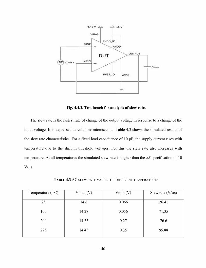
Fig. 4.4.2. Test bench for analysis of slew rate............................................................................. 40
Fig. 5.1.1. The layout of the op amp (Length = 431.6 µm; Width = 738 µm). ............................ 42
Fig. 5.1.2. NMOS input pair transistor matching. ........................................................................ 44
Fig. 5.1.3. Current mirror (M3 & M4) layout. .............................................................................. 44
Fig. 5.1.4. Current mirror (M5 & M7) layout. .............................................................................. 45
Fig. 5.1.5. Final chip layout with padframe and pin connections. ................................................ 46
Fig. 5.1.6. Die micrograph of the fabricated op amp. ................................................................... 47
Fig. 6.1.1. Bonding plan................................................................................................................ 49
Fig. 6.1.2 Final packaged chip. ..................................................................................................... 50

Fig. 6.2.1 Probe station test setup. ................................................................................................ 51
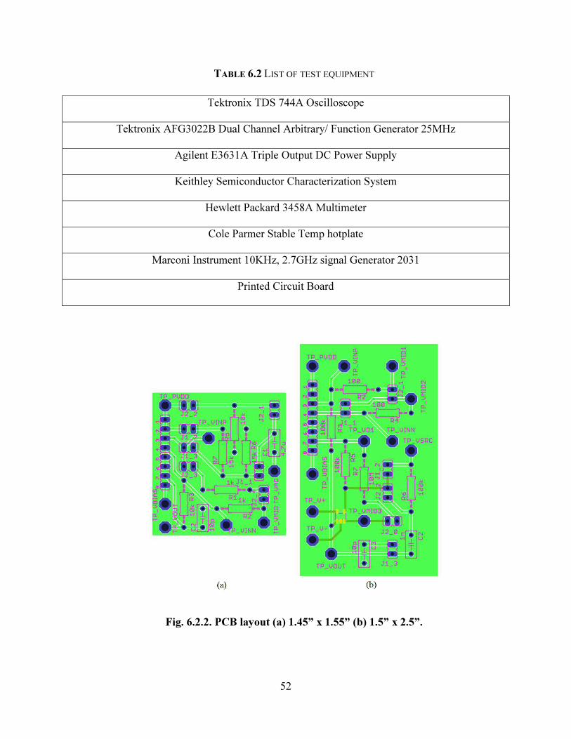
Fig. 6.2.2. PCB layout (a) 1.45” x 1.55” (b) 1.5” x 2.5”. ............................................................. 52
Fig. 6.3.1 Wafer diagram .............................................................................................................. 53
Fig. 6.3.2 DC bias sweep. ............................................................................................................. 54
Fig. 6.3.3. The offset voltage at different temperatures ................................................................ 55
Fig. 6.3.4. Input common mode range at 25 °C. ........................................................................... 55
Fig. 6.3.5 Input common mode range at 300 °C. .......................................................................... 56
Fig. 6.3.6. Slew rate measurement at 25 °C. ................................................................................. 58
Fig. 6.3.7. DC gain measurement at 25 °C. .................................................................................. 59
Fig. A.C.1. Input offset voltage measurement .............................................................................. 66
Fig. A.C.2 ICMR measurement circuit ......................................................................................... 68
Fig. A.D.1. Open loop gain test bench .......................................................................................... 69
Fig. A.D.2. Test bench for power dissipation and unity gain bandwidth ..................................... 70
Fig.A.D.3. CMRR test bench ........................................................................................................ 71
Fig. A.D.4. PSRR test bench......................................................................................................... 72
Fig. A.E.1. Slew rate test bench .................................................................................................... 73
Fig. B.1. Three stage op amp schematics...................................................................................... 74

LIST OF TABLES
TABLE 1.1 NON IDEAL LINEAR CHARACTERISTICS OF OP AMP .......................................................... 3
TABLE 3.1 OPERATIONAL AMPLIFIER DESIGN SPECIFICATIONS ....................................................... 15
TABLE 3.2 PROCESS PARAMETERS ................................................................................................. 23
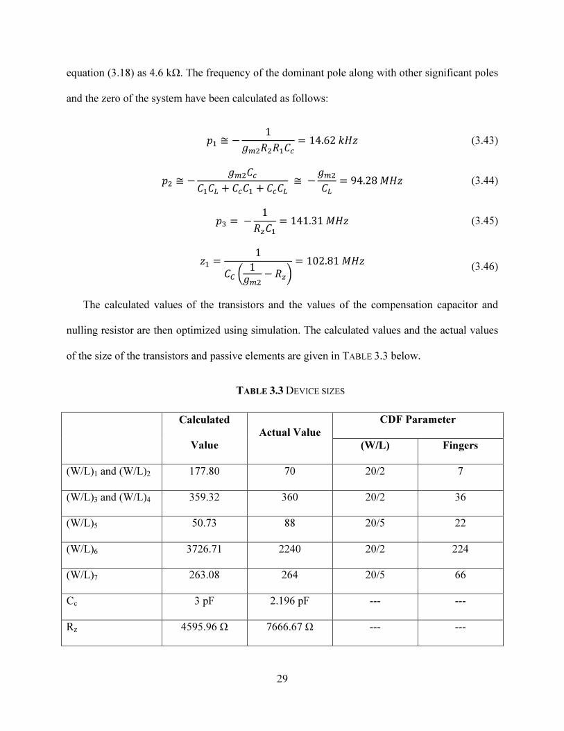
TABLE 3.3 DEVICE SIZES ................................................................................................................ 29
TABLE 4.1 DC SIMULATION CHARACTERISTICS.............................................................................. 35
TABLE 4.2 AC SIMULATION CHARACTERISTICS.............................................................................. 37
TABLE 4.3 AC SLEW RATE VALUE FOR DIFFERENT TEMPERATURES ............................................... 40
TABLE 5.1 THE INPUT AND OUTPUT PINS OF OP AMP WITH DESCRIPTION ........................................ 42
TABLE 6.1 THE BONDING DIAGRAM PIN CONFIGURATIONS ............................................................. 49
TABLE 6.2 LIST OF TEST EQUIPMENT .............................................................................................. 52
TABLE 6.3 OP AMP DC CHARACTERISTICS MEASUREMENTS .......................................................... 57
TABLE 6.4 OP AMP AC AND TRANSIENT CHARACTERISTICS MEASUREMENTS ................................ 60

1
CHAPTER 1
INTRODUCTION
An operational amplifier (op amp) is the primary building block in analog and mixed-signal
integrated circuits (ICs) and systems. It has a vast range of applications including DC bias
generation, data conversion, sensor circuits, high-speed amplification and filtering. The op amp
has several electrical characteristics such as, offset, gain-bandwidth (GB), slew rate, input
common mode range (ICMR), as well as frequency response characteristics such as phase
margin, that need to be considered during the design process [1]. At high temperatures (greater
than 225 oC) the performance parameters show promising results when silicon (Si) and silicon-
on-insulator (SOI) based devices are limited by leakage to operation at 125 oC and 225
oC,
respectively [2]. The main objective of this thesis is the design of a SiC Complementary Metal
Oxide Semiconductor (CMOS) op amp that is capable of reliable operation at high temperatures
(25 °C to more than 300 °C) where Si and SOI ICs cannot perform well.
This thesis presents a two-stage op amp designed to drive a small purely capacitive load
using an analog/mixed-signal SiC CMOS Process Design Kit (PDK) developed by Ozark IC and
the University of Arkansas students who were a part of NSF-BIC project [3]. A three-stage op
amp has also been designed in the next design cycle to provide more functionality and improved
performance. The future implementation of the op amp circuit is used in, but not limited to,
protection circuitry of a high temperature SiC gate driver.
2
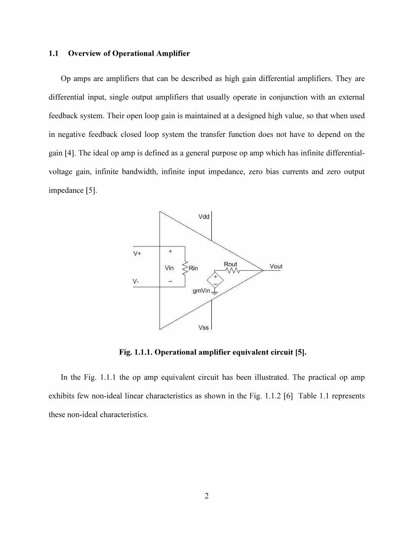
1.1 Overview of Operational Amplifier
Op amps are amplifiers that can be described as high gain differential amplifiers. They are
differential input, single output amplifiers that usually operate in conjunction with an external
feedback system. Their open loop gain is maintained at a designed high value, so that when used
in negative feedback closed loop system the transfer function does not have to depend on the
gain [4]. The ideal op amp is defined as a general purpose op amp which has infinite differential-
voltage gain, infinite bandwidth, infinite input impedance, zero bias currents and zero output
impedance [5].
Fig. 1.1.1. Operational amplifier equivalent circuit [5].
In the Fig. 1.1.1 the op amp equivalent circuit has been illustrated. The practical op amp
exhibits few non-ideal linear characteristics as shown in the Fig. 1.1.2 [6] Table 1.1 represents
these non-ideal characteristics.

3
TABLE 1.1 NON IDEAL LINEAR CHARACTERISTICS OF OP AMP
Parameter Symbol Unit
Differential input resistance Rid Ω
Differential input capacitance Cid fF
Common mode input resistance Ricm Ω
Input offset voltage Vos mV
Input bias currents Ib1 & Ib2 nA
Common mode rejection ratio CMRR ---
Voltage noise spectral density en2 mean sq volts/Hz
Current noise spectral density in2 mean sq amps/Hz
Fig. 1.1.2. Non-ideal linear characteristics of op amp [6].

4
One of the advantages of a CMOS op amp is that in negative feedback the common mode
characteristics can be ignored. Also, the values of Rid, Ricm, Ib1 and Ib2 can be ignored easily due
to the high input resistance of the MOS devices [6]. The output voltage Vout can be expressed as a
sum of the differential portion, Av(s), and the common-mode portion, Ac(s) as shown in below,
= − ± + 2
(1.1)
= (0) − 1 − 1 − 1… (1.2)
Here p1, p2, p3,… are the poles of the differential-frequency response.
The unity-gain bandwidth (GB) characteristics can be defined as the frequency where the
frequency response curve crosses the 0 dB line. In other words if the dominant pole is p1 and the
DC gain is Av(0) then,
= 0. | | (1.3)
Other characteristics of interest are the Power Supply Rejection Ratio (PSRR) and the
Common Mode Rejection Ratio (CMRR), which are defined in equation (1.4) and equation (1.5)
respectively,
=∆∆ =
= 0 ( = 0)
(1.4)
= 20 log 00 (1.5)
The input common mode range (ICMR) is the allowable voltage range of the input common-
mode signal and the slew rate (SR) is the rate of change of the output voltage (measured in

5
volts/s) due to an abrupt change in the input voltage. ICMR and SR are large signal
characteristics.
1.2 Applications
The op amp has vast applications in signal processing and mixed-signal systems, where it is
commonly used in the interface between the differential input stage and the analog to digital
converters (ADC). Due to the available high temperature functionality of SiC CMOS op amps,
they are a good match to use for signal conditioning and sensor circuitry of SiC-based power
switching devices. A few of the major applications of op amps and operational transconductance
amplifiers (OTAs) are active filters, data converters, sensors, signal conditioning and signal
amplifiers [7]. Some of the applications of op amps are described briefly below:
1.2.1 2nd order Active Low Pass Filter
Op amps and OTAs are used as an active element in signal processing and filter design as
they provide high frequency operation with less sensitivity and simpler circuit topology [8]. The
schematics of a 2nd
order active low pass filter are shown in Fig. 1.2.1 below. The circuit has low
quality factor sensitivity and low natural frequency when compared with passive filters.

6
Fig. 1.2.1. 2nd
order active low pass filter [8].
1.2.2 Digital to Analog Data Converters
Op amps have applications in data converters, both digital to analog converters (DAC) and
analog to digital converters (ADC). The primary advantage of using an op amp in DAC is that
the output load can be any arbitrary value rather than a fixed known capacitive value [9]. Fig.
1.2.2 shows the schematics of a traditional current mode R-2R ladder DAC. The required phase
margin of the op amp is set very high (90°) to have a fast settling time. The output swing can be
increased by increasing the open-loop gain or speed or by adding another op amp.

7
Fig. 1.2.2. Current mode R-2R DAC [9].
1.2.3 High-Side Current Sensing Circuit
The principle of the high side current sensor for a power switch converter is that it detects the
current through the measured path and converts it to a proportional voltage. Fig. 1.2.3 shows the
schematics of a current sensor with single op amp difference amplifier. The op amp detects and
amplifies the voltage through the sensing resistor (RSEN) and produces the measurable output
(Vout) [10]. High-side current sensing is required to monitor the accidental short circuit current
detection for the protection circuitry in power conversion systems. One of the major advantages
of using op amps in this type of circuitry is low cost, low power dissipation and high common
mode rejection ratio.

8
Fig. 1.2.3. Current sensor with single op amp difference amplifier [10].
1.3 Silicon Carbide CMOS Technology
SiC is a wide bandgap semiconductor material that can operate in temperatures up to 450 °C
[11]. A SiC CMOS integrated circuit (IC) technology has applications in automotive, aerospace
and deep well drilling as well as in SiC power electronics. The high temperature sensors and
signal processing circuits that can be built using a SiC CMOS op amp will be beneficial for these
systems [11]. The 15-V SiC CMOS technology used for this work is presented here. The process
parameters are given below:
• Operating temperature up to 400 °C
• 1.2 µm minimum feature size, single metal process
• 40 nm electrical oxide equivalent thickness
• 15 V gate to source operating voltage

Fig. 1.3
Fig. 1.3.1 shows the SiC CMOS process archite
wafer with a doped epi-layer. The process includes epitaxial deposition and ion im
form the p- and n- regions. Further ion implantation process took place to create p+ and n+
source/drain regions and threshold voltage adjustment
Afterwards the gate dielectrics, thick field oxide and the polysilicon gate electrodes a
developed. The p+ and n+ regions will have ohmic metal contacts build followed by the
deposition of patterned refractory metal interconnect. The last step
to form a passivation layer.
1.4 Thesis Organization
The organization of the thesis is as follows:
have been considered for the design process
selected topology along with the specifications, equations and hand cal
presented. Chapter 4 covers the simulation
temperature and corners. This is followed by Chapter 5 which presents the actual layout of the
designed op amp. Chapter 6 covers the
results at different temperatures
recommendations for future work.
9
1.3.1. SiC CMOS process architecture.
shows the SiC CMOS process architecture. The substrate is an n+ 4H SiC Si
layer. The process includes epitaxial deposition and ion im
regions. Further ion implantation process took place to create p+ and n+
source/drain regions and threshold voltage adjustment. All implants are annealed together.
the gate dielectrics, thick field oxide and the polysilicon gate electrodes a
The p+ and n+ regions will have ohmic metal contacts build followed by the
deposition of patterned refractory metal interconnect. The last step in the process technology
thesis is as follows: Chapter 2 covers the different topologies that
have been considered for the design process. In Chapter 3 the actual design process for the
selected topology along with the specifications, equations and hand calculation has been
Chapter 4 covers the simulation of the DC, AC and transient analysis in different
temperature and corners. This is followed by Chapter 5 which presents the actual layout of the
. Chapter 6 covers the packaging information, the test setups and
different temperatures. Finally, Chapter 7 covers the conclusion and the
recommendations for future work.
cture. The substrate is an n+ 4H SiC Si-faced
layer. The process includes epitaxial deposition and ion implantation to
regions. Further ion implantation process took place to create p+ and n+
annealed together.
the gate dielectrics, thick field oxide and the polysilicon gate electrodes are
The p+ and n+ regions will have ohmic metal contacts build followed by the
in the process technology is
different topologies that
In Chapter 3 the actual design process for the
culation has been
of the DC, AC and transient analysis in different
temperature and corners. This is followed by Chapter 5 which presents the actual layout of the
formation, the test setups and practical
covers the conclusion and the

10
CHAPTER 2
OPERATIONAL AMPLIFIER TOPOLOGIES
The operational amplifier can be implemented using a variety of topologies depending on the
application requirements, process parameters, frequency mode, required characteristic
performance and the degree of complexity available. Based on each specific design application,
different topologies have been developed. Special considerations have been taken to study
topologies that are most reliable and have a low level of complexity since the process technology
in use is still in a developing stage. Research on previously developed topologies has been
analyzed in this chapter.
2.1 Two-Stage Miller Compensated CMOS Op Amp
One of the basic structures of an op amp is the two stage CMOS op amp. In this structure the
first stage is the differential transconductance stage which provides most of the op amp gain,
followed by the second stage, which is a common source stage, that mainly provides a large
output swing as [4] shown in the Fig. 2.1.1.
Fig. 2.1.1. Block diagram of a two-stage op amp [4].

Here the differential to single
stage is not followed by any buffer stage (
both amplifier stages are properly biased
mirror or a beta multiplier as the
the stability issue that arises when used in
compensation can be accomplished
the second amplifier stage. This creates a
pole splitting technique [12]. Th
response further away from the origin of the complex frequency plane,
dominant pole which will move closer to the origin. This will also create a
(RHP) zero which can be positioned
overall schematic of the topology is presented in
two-stage system are its robustness and the simplicity. They are the most widely used topology
and heavily reliable with a new process technology
Fig. 2.1.2. Unbuffered
11
single-ended conversion takes place in the first stage and
stage is not followed by any buffer stage (the output resistance is very high). The transistors in
both amplifier stages are properly biased to operate in the saturation region by
the biasing circuit. The circuit needs a compensation strategy due to
the stability issue that arises when used in a closed-loop negative feedback system. The
can be accomplished by using Miller techniques where a capacitor is place
stage. This creates a feedback path through the capacitor and employs the
. This technique moves the poles of the open loop frequency
he origin of the complex frequency plane, with the exception of the
dominant pole which will move closer to the origin. This will also create a
positioned by placing a nulling resistor in series with the capacitor. The
overall schematic of the topology is presented in Fig. 2.1.2 below. The main advantage
robustness and the simplicity. They are the most widely used topology
and heavily reliable with a new process technology [13].
Unbuffered, two-stage CMOS op amp schematic
place in the first stage and the output
the output resistance is very high). The transistors in
to operate in the saturation region by using a current
. The circuit needs a compensation strategy due to
loop negative feedback system. The
by using Miller techniques where a capacitor is placed across
path through the capacitor and employs the
poles of the open loop frequency
with the exception of the
dominant pole which will move closer to the origin. This will also create a right-half plane
by placing a nulling resistor in series with the capacitor. The
below. The main advantages of the
robustness and the simplicity. They are the most widely used topology
stage CMOS op amp schematic.

12
2.2 Three-Stage Nested Miller Compensation CMOS Op Amp
The three-stage op amp is used in analog and mixed-signal circuits to achieve higher DC gain
and low power consumption from the supply voltage [9]. The block diagram of the three-stage
nested Miller compensated (NMC) op amp is shown in Fig. 2.2.1. The circuit has three amplifier
stages for high DC gain and two capacitors for stability. The capacitors create the frequency
compensation needed for stability [14].
Fig. 2.2.1. Three-stage NMC op amp block diagram [14].
The first two stages of the Fig. 2.2.1 can be assumed to be a cascade of two differential
amplifiers followed by the third stage which can be a common source amplifier. The Fig. 2.2.2
shows an actual topology of a three-stage op amp. Here the capacitors are placed in such a way
so that the feedback current through Cc1 combines with the feedback current through Cc2 and
flows towards the first stage. So, the compensation techniques implemented in Fig. 2.2.2 are an
indirect nested Miller compensation method [9]. The main advantage of this topology is that, by

13
using two differential amplifier stages, all of the transistors in the topology are biased with
known currents.
Fig. 2.2.2. Three-stage op amp schematic [9].

14
CHAPTER 3
CMOS OPERATIONAL AMPLIFIER DESIGN
3.1 Design Procedure
The design flow of the CMOS operational amplifier includes defining the requirements of the
amplifier, defining the process design kit, stating the targeted inputs and outputs, hand
calculations, simulations, layout, fine tuning the circuit based on parasitics, fabrication and
testing. For a successful design the designer should have a clear idea about the needs of the
system and each step of the design procedure. It is the designer’s responsibility to successfully
execute all the steps to ready the design for fabrication.
The general steps for integrated circuit design according to [6] are presented below:
1. Definition of the function and performance capability of the design: CMOS operational
amplifier design for high temperature performance.
2. Synthesis or implementation: Silicon Carbide CMOS process.
3. Simulation or modeling: Estimate the device parameters based on hand calculations. Run
simulation under different corners and temperature range to confirm the defined
characteristic specifications.
4. Geometrical description: Complete the layout using proper toolchain and perform the
design rule check.

15
5. Simulation including the geometrical parasitics: Consider the parasitic effects introduced
by the layout and re-simulate the amplifier to reconfirm the performance characteristics.
6. Fabrication: When confident with the results of 1-5 above, the circuit is submitted for
fabrication.
7. Testing & Verification: Develop the test and verification plan. Test the amplifier in real
world scenario and compare with simulation results.
At this point, the next design process begins by adding the amplifier improvements identified
from test data analysis obtained from the first fabrication run.
3.2 Design Specifications
TABLE 3.1 OPERATIONAL AMPLIFIER DESIGN SPECIFICATIONS
Parameter Symbol Value Unit
Supply Voltage AVDD 15 V
Temperature Range TA 25 – 300 oC
Gain AV 60 dB
Gain Bandwidth GB 5 MHz
Phase Margin P.M. 45 Degree
Slew Rate SR 10 V/µs
Input Common Mode Range ICMR 5 – 14 V
Output Voltage Swing ∆Vout 2 – 14 V
Load Capacitance CL 10 pF

16
The key design specifications of the CMOS SiC op amp are given in Table 3.1. The primary
motivation of the design process was to have a functional operational amplifier in a CMOS SiC
process. For this reason, the degree of complexity has been kept at minimum and the design
specifications were targeted rationally. Due to the high threshold voltages of the MOSFETs in
the SiC process the supply voltage is higher than usual (15 V). The capacitive load has been
specified as 10 pF so that the amplifier would be able to drive the load capacitances of testing
equipment, i.e. oscilloscope probes. The circuit must work properly over a wide range of
temperature while maintaining a high CMRR and PSRR within an acceptable input common-
mode range.
3.3 Circuit Design
The CMOS SiC operational amplifier has two stages. One differential input stage followed
by a common-source amplifier output stage. An additional compensation circuit is added
between these two stages for better stability and improved phase margin. The biasing of the
circuit is accomplished by using an external voltage source to reduce the circuit complexity and
to have a better control over the circuit quiescent point. The circuit does not include any buffer
stage and thus the load has been kept as a small capacitive value. The complete circuit schematic
is shown in Fig. 3.1.
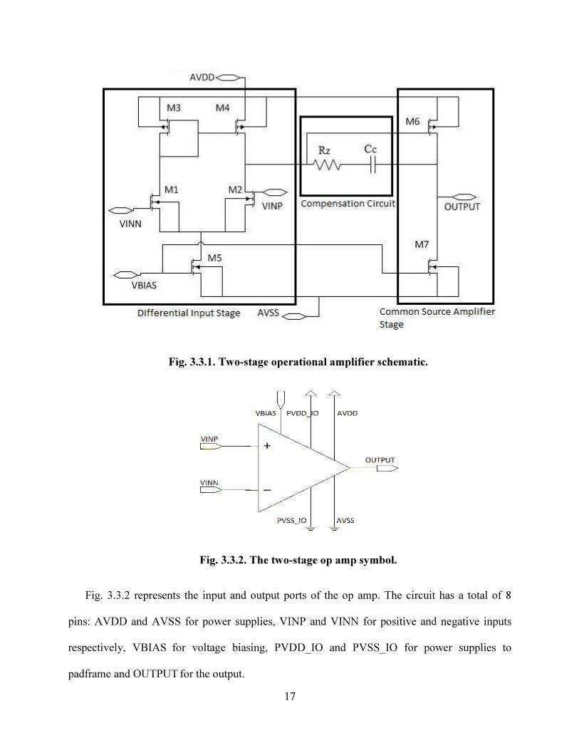
Fig. 3.3.1.
Fig.
Fig. 3.3.2 represents the input and output ports of the
pins: AVDD and AVSS for power supplies, VINP and VINN for positive and negative inputs
respectively, VBIAS for voltage biasing, PVDD_IO and PVSS_IO for power supplies to
padframe and OUTPUT for the output.
17
Two-stage operational amplifier schematic.
Fig. 3.3.2. The two-stage op amp symbol.
represents the input and output ports of the op amp. The circuit has a total of 8
pins: AVDD and AVSS for power supplies, VINP and VINN for positive and negative inputs
r voltage biasing, PVDD_IO and PVSS_IO for power supplies to
for the output.
amp. The circuit has a total of 8
pins: AVDD and AVSS for power supplies, VINP and VINN for positive and negative inputs
r voltage biasing, PVDD_IO and PVSS_IO for power supplies to

18
3.3.1 Compensation Circuit
The compensation circuit is placed between the input and output of the second stage. It
consists of a compensation capacitor (Miller capacitor) in series with a resistor (nulling resistor)
as shown in Fig. 3.3.3. The purpose of the Miller capacitor is to introduce Miller feedback to
obtain a single time-constant, dominant pole amplifier and the purpose of the nulling resistor is
to position the right-half plane zero of the system created by the Miller feedback.
Fig. 3.3.3. Compensation circuit.
The Miller effect can be defined as the increase in the effective capacitance of the input of
second stage because of the amplification through the feedback path created by the Miller
capacitance. The associated pole due to Miller capacitor moves near the origin of the complex
frequency plane and acts as a dominant pole. This reduces the bandwidth of the amplifier while
improving the phase margin. Another advantage of the Miller effect is that the output pole of the
system moves further away from the origin of the complex frequency plane due to the pole
splitting technique. This reduces the output resistance of the circuit and improves the op amp
stability.

19
The capacitance Cc in the feedback path produces a zero in the right-half portion of the
complex frequency plane. This right-half plane (RHP) zero increases the magnitude and
decreases the phase and behaves like a left-half plane (LHP) pole and a left-half plane zero.
Thus, by selecting the value of the nulling resistor Rz the effect of the RHP zero has been
minimized. This increases the gain bandwidth by moving all the poles and zeros except the
dominant pole away from the unity-gain bandwidth frequency. The small-signal model of the
system with the compensation circuit is shown in Fig. 3.3.4. Fig. 3.3.5 is the electrical equivalent
circuit of Fig. 3.3.4.
Fig. 3.3.4. Small-signal model of two-stage op amp with Miller compensation.
Fig. 3.3.5. Electrical equivalent model of two-stage op amp.
20
The additional input impedance due to Miller effect is ZM and the additional output
impedance is ZMo.
= 1 − (3.1)
= 1 − 1
(3.2)
= 1 (3.3)
= 1 − 1 + (3.4)
= 1 − 1/1 + (3.5)
Now applying Kirchhoff’s Current Law, following node voltages are obtained:
!"# + 11 + 11 + $ 1 + % 1 − = 0 (3.6)
!1 + 2 + + $ 1 + % − 1 = 0 (3.7)
The small-signal transfer function of the circuit has been given by using Cramer’s rule,
()"#() ≈
&1 − '$ 1 !2% − ()
1 + + + + +
(3.8)
= (3.9)
The op amp’s poles and zero can be found to be in (3.10) – (3.13). Here p1 is the dominant
pole frequency.
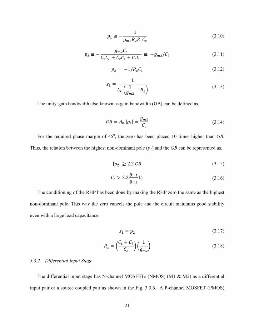
21
≅ −1 (3.10)
≅ − + + ≅ − / (3.11)
= −1/ (3.12)
= 1
$ 1 − %
(3.13)
The unity-gain bandwidth also known as gain bandwidth (GB) can be defined as,
= | | = (3.14)
For the required phase margin of 45o, the zero has been placed 10 times higher than GB.
Thus, the relation between the highest non-dominant pole (p2) and the GB can be represented as,
| | ≥ 2.2 (3.15)
> 2.2
(3.16)
The conditioning of the RHP has been done by making the RHP zero the same as the highest
non-dominant pole. This way the zero cancels the pole and the circuit maintains good stability
even with a large load capacitance.
= (3.17)
= $ + % $ 1
% (3.18)
3.3.2 Differential Input Stage
The differential input stage has N-channel MOSFETs (NMOS) (M1 & M2) as a differential
input pair or a source coupled pair as shown in the Fig. 3.3.6. A P-channel MOSFET (PMOS)

22
current mirror load, consisting of M3 & M4, is placed at the top. The purpose of the current
mirror is to create a current to voltage conversion stage. The biasing of the source coupled pair is
done with a current sink (M5) placed at the bottom. The gate of the M5 transistor is connected
with an external voltage source for fine tuning the biasing voltage.
Fig. 3.3.6. Differential input stage.
When all the transistors are in saturation region and the differential input signal is zero the
current at the output node, I1, will be zero and the input device currents will be the same in both
input branches and equal to I5/2. This current along with the Miller capacitor Cc decides the
internal slew rate (SR), which is given below,
=* (3.19)
The process parameters are given in the table below.

23
TABLE 3.2 PROCESS PARAMETERS
Parameter
NMOS PMOS
Channel
Length
L = 2 µm
Channel
Length
L = 5 µm
Channel
Length
L = 2 µm
Channel
Length
L = 5 µm
Threshold Voltage (VT) 2.9 V 3 V -3.45V -3.65 V
Transconductance Parameter (K’) 1 µA/V2 0.8 µA/V
2 0.46 µA/V
2 0.3 µA/V
2
Channel Length Modulation (λ) 0.733 V–1
0.733 V–1
0.493 V–1
0.493 V–1
The W/L ratios of the transistors are calculated by implementing the drain current equations
and the process parameters. The drain current equation of an n-channel MOSFET is given below,
* =1
2+ ,- − (3.20)
The drain current equation of a p-channel MOSFET is given below,
* = 1
2+ ,- . − //0 (3.21)
The equations for the transconductance (gm), transistor’s drain to source resistance and
transistor’s saturation voltage between the drain-source are represented below,
= 12+ $,- % * =2* (3.22)
2 = 1 = 1*3 (3.23)

24
() = − || = 1 2*+ ,- (3.24)
The Input Common Mode Range (ICMR) of the circuit is determined by the NMOS input
pair. The maximum limit of the ICMR, VIC (max) is determined by the saturation voltage limit of
the M3 & M4 transistors. The maximum common mode input voltage can be represented from
[6] as
!45 = 66 − − || + (3.25)
max = 15V − 0.55 − 3.45 + 2.9 = 13.9 (3.26)
The minimum ICMR is limited by the saturation voltages of the M1, M2 and the M5
transistors. The minimum common mode input voltage, VIC (min), can be represent from [6] as,
!"# = + 4 + + (3.27)
!"# = 0V + 1.19 + 0.85 + 2.9 = 4.94 (3.28)
Thus, the total input common mode range can be expressed as 4.94 V ≤ VIC ≤ 13.9 V, which
is very close to the specified ICMR.
The majority of the open loop voltage gain (≈40 dB) has been achieved in the input stage.
The small-signal analysis of the input stage differential amplifier has been performed to calculate
the small-signal voltage gain and output resistance of the input stage. Fig. 3.3.7 shows the small-
signal model of the input stage. Here the input branches have been assumed as perfectly matched
on both sides.
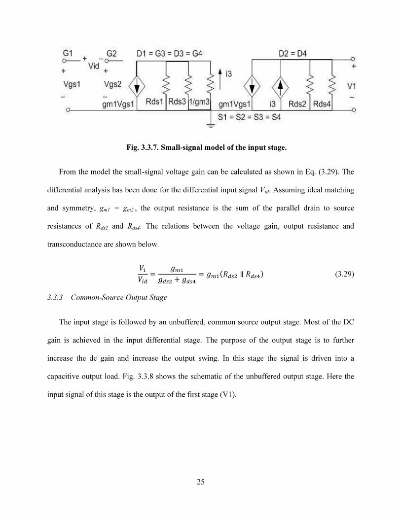
25
Fig. 3.3.7. Small-signal model of the input stage.
From the model the small-signal voltage gain can be calculated as shown in Eq. (3.29). The
differential analysis has been done for the differential input signal Vid. Assuming ideal matching
and symmetry, gm1 = gm2., the output resistance is the sum of the parallel drain to source
resistances of Rds2 and Rds4. The relations between the voltage gain, output resistance and
transconductance are shown below.
= + = ∥ (3.29)
3.3.3 Common-Source Output Stage
The input stage is followed by an unbuffered, common source output stage. Most of the DC
gain is achieved in the input differential stage. The purpose of the output stage is to further
increase the dc gain and increase the output swing. In this stage the signal is driven into a
capacitive output load. Fig. 3.3.8 shows the schematic of the unbuffered output stage. Here the
input signal of this stage is the output of the first stage (V1).

Fig.
When the differential input equals to zero, the output should also be zero
does not have any systematic input offset voltage
amplifier currents I6 and I7 should be equal.
For proper biasing, all of the transistors in
M6 and the pair M5, M7 create two mirroring currents. Now, to have proper mirroring between
M4 and M6, VSG4 = VSG6. And to have proper mirroring betwe
,
26
Fig. 3.3.8. Common-source output stage.
When the differential input equals to zero, the output should also be zero so that the op amp
does not have any systematic input offset voltage. This means when I2 = I4 = ½ I
should be equal.
For proper biasing, all of the transistors in Fig. 3.3.1 have to be in saturation. The pair M4,
M6 and the pair M5, M7 create two mirroring currents. Now, to have proper mirroring between
. And to have proper mirroring between M5 and M7, VGS5
,
2
so that the op amp
= ½ I5, the output
have to be in saturation. The pair M4,
M6 and the pair M5, M7 create two mirroring currents. Now, to have proper mirroring between
GS5 = VGS7.
(3.30)
(3.31)
(3.32)
(3.33)

27
The maximum and minimum output swing of the op amp are determined from the output
stage. The maximum output swing is limited by the minimum saturation drain-to-source voltage
of M6 before going to the active region. The minimum output swing is limited by the minimum
saturation drain-to-source voltage of M7 before going to the active region.
= − ! (3.34)
= 15 − 0.7 = 14.3 (3.35)
= + " (3.36)
= 0 + 1.4 = 1.4 (3.37)
Using the small-signal model, the small-signal output resistance and small-signal voltage
gain of the output stage can be calculated. The small-signal model of the common source
amplifier stage is presented in Fig. 3.3.9 below.
Fig. 3.3.9. Small-signal model of common source output stage.
Considering gm6 = gm2 the small-signal voltage gain and resistance equation is shown below.
=
! + " = ! ∥ " (3.38)
Thus the overall op amp gain can be represented as,
∗
= + ! + " = (3.39)

28
∗
= 807 (3.40)
And the total power dissipation of the circuit can be represent as,
= * + *! + || (3.41)
= 50 + 260μ ∗ 15 = 4.65!, (3.42)
The BSIM3 device model developed for the SiC process was used for simulation. The
scalability of this model was limited such that the allowable width (W) of each of the transistors
was set to a fixed value (20 µm) and the value of the length (L) was selected as either 2 µm or 5
µm depending on the transistor functions. For example, the L = 2 µm devices have higher
transconductance (gm) values, so they are good for devices which need high gain. The L = 5 µm
devices have higher output resistance, which makes them better for matching circuits where the
current stays constant with the changes in the drain voltage. For this the NMOS source coupled
pair (M1 and M2) and the PMOS current mirror load (M3 and M4) of the 1st stage and the
PMOS (M6) of the 2nd
stage have device length L = 2 µm and the current sink of the 1st stage and
the NMOS (M7) of the 2nd
stage have device length L = 5 µm.
The value of the compensation capacitor was calculated as 3 pF. The calculated tail current
of first stage was 50 µA and the calculated current in the second stage was 260 µA. The (W/L)
ratios of the NMOS source coupled pair were calculated as 70 from GB specifications. And the
(W/L) ratios of the PMOS current mirror and the NMOS current sink were calculated from the
ICMR specifications as 360 and 88 respectively. For the required phase margin the non-
dominant poles has been placed at least 10 times the GB. From this the (W/L) of the PMOS (M6)
acquired as 3726. The (W/L) of the NMOS (M7) were calculated from the systematic offset
requirement as 263. Lastly the value of the nulling resistor Rz has been calculated by using the
29
equation (3.18) as 4.6 kΩ. The frequency of the dominant pole along with other significant poles
and the zero of the system have been calculated as follows:
≅ −1 = 14.6289 (3.43)
≅ − + + ≅ − = 94.289 (3.44)
= − 1 = 141.319 (3.45)
= 1
$ 1 − % = 102.819
(3.46)
The calculated values of the transistors and the values of the compensation capacitor and
nulling resistor are then optimized using simulation. The calculated values and the actual values
of the size of the transistors and passive elements are given in TABLE 3.3 below.
TABLE 3.3 DEVICE SIZES
Calculated
Value
Actual Value
CDF Parameter
(W/L) Fingers
(W/L)1 and (W/L)2 177.80 70 20/2 7
(W/L)3 and (W/L)4 359.32 360 20/2 36
(W/L)5 50.73 88 20/5 22
(W/L)6 3726.71 2240 20/2 224
(W/L)7 263.08 264 20/5 66
Cc 3 pF 2.196 pF --- ---
Rz 4595.96 Ω 7666.67 Ω --- ---

30
CHAPTER 4
SIMULATION OF THE OPERATIONAL AMPLIFIER
The performance of the designed op amp was evaluated and optimized by simulation. Test
benches were developed to verify different circuit characteristics performance over different
process corners (Typical, Fast-Fast, Slow-Slow) and over temperature (25 °C to 275°C). These
variations in the process corners imply different drive strengths of the NMOS and PMOS
transistors. For example a fast-fast corner means both the NMOS and PMOS transistors have low
threshold voltages. The simulations were run using the Synopsys HSPICE simulator. The utilized
models were developed based on BSIM3 device models and the high fidelity process design kit
was created as part of NSF-BIC project. The simulation setup, design tool chain and the AC, DC
and transient performance analysis will be presented in this chapter.
4.1 Simulation Setup
The simulation setup was created to measure and verify every performance characteristics
(DC, AC and transient responses) of op amp in a close approximation of real world
environments. Every test bench was designed to calculate some specific performance of the op
amp and for this, additional passive elements such as resistors and capacitors were included to
recreate a real life test setup. The schematics of the test setups include the input signals, power
supply, the input bias voltage and the output load capacitance for each test circuit. Due to the
high threshold voltages of the transistors in SiC, the power supply is 15 V, the bias voltage for
31
every simulation was calculated as 4.45 V and the common mode voltage VICM was taken as 7 V
or around mid-rail.
4.2 DC Simulation
DC simulation was used to characterize the following specifications: input offset voltage, the
DC power dissipation, the input common mode range and the output voltage range (OVR). The
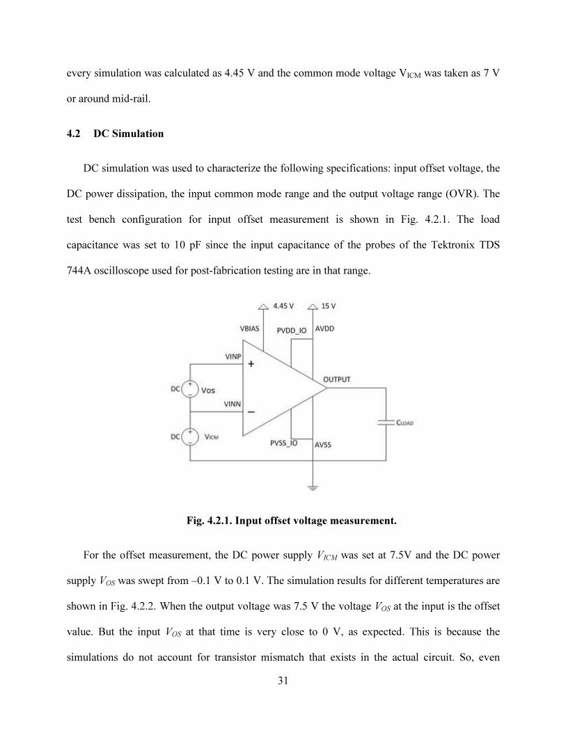
test bench configuration for input offset measurement is shown in Fig. 4.2.1. The load
capacitance was set to 10 pF since the input capacitance of the probes of the Tektronix TDS
744A oscilloscope used for post-fabrication testing are in that range.
Fig. 4.2.1. Input offset voltage measurement.
For the offset measurement, the DC power supply VICM was set at 7.5V and the DC power
supply VOS was swept from –0.1 V to 0.1 V. The simulation results for different temperatures are
shown in Fig. 4.2.2. When the output voltage was 7.5 V the voltage VOS at the input is the offset
value. But the input VOS at that time is very close to 0 V, as expected. This is because the
simulations do not account for transistor mismatch that exists in the actual circuit. So, even

32
though there seems no significant offset voltage present in the simulation, in real life testing
some offset will be present.
Fig. 4.2.2. Simulation results of input offset voltage and output voltage swing.
The next DC characteristics that were simulated were the ICMR and OVR. Fig. 4.2.4 shows
the test setup configuration. Here the op amp is placed in a voltage-follower configuration.
Fig. 4.2.3. Op amp in voltage-follower configuration.
0.001.002.003.004.005.006.007.008.009.0010.0011.0012.0013.0014.0015.0016.00
-0.1 -0.05 0 0.05 0.1 0.15
Vou
t (V
)
Vos (V)
Offset Voltage
/output T = 25
/output T = 100
/output T = 200
/output T = 275

33
In the voltage follower configuration (as a unity-gain buffer), the output of the amplifier is
connected with its negative input. This forces the output to be equal to the input voltage when the
op-amp functions. The simulation results of the voltage follower at 25 °C and at 275 °C are
shown in Fig. 4.2.4 and Fig. 4.2.5 respectively.
Fig. 4.2.4. Simulation results of voltage follower at T = 25 °C.
Fig. 4.2.5. Simulation results of voltage follower at T = 275 °C.
0.00E+00
5.00E-05
1.00E-04
1.50E-04
2.00E-04
2.50E-04
3.00E-04
3.50E-04
4.00E-04
4.50E-04
0.001.002.003.004.005.006.007.008.009.00
10.0011.0012.0013.0014.0015.00
0 5 10 15
Vou
t (V
)
Vin (V)
ICMR & OVR plot for T = 25 °C
output
I_supply
I_su
pp
ly (
A)
0.00E+00
2.00E-04
4.00E-04
6.00E-04
8.00E-04
1.00E-03
1.20E-03
1.40E-03
1.60E-03
1.80E-03
2.00E-03
0.001.002.003.004.005.006.007.008.009.00
10.0011.0012.0013.0014.0015.0016.00
0 5 10 15
Vou
t (V
)
Vin (V)
ICMR & OVR plot for T = 275 °C
/output Y
I_supply
I_su
pp
ly (
A)

34
From the simulation data the ICMR of the op amp was found to be 4.7 V to 14.58 V at 25 °C
and 4.87 V to 14.22 V at 275 °C. The OVR at 25 °C is 690 mV to 14.45 V and at 275 °C is 980
mV to 14.12 V. But in the open loop configuration, the maximum allowable input common
mode voltage (14.58 V at 25 °C and 14.22 V at 275 °C) does not provide acceptable gain (gain is
less than 55dB). So for the open loop mode, the maximum input common mode voltage is 13.7 V
at 25 °C and 10.34 V at 275 °C (allowing at least 55dB gain). At room temperature the ICMR is
within the specification but at the high temperatures the threshold voltages of the transistors
shifts and the maximum input common mode voltages is less than the specifications.
The total DC power consumption was measured by measuring the dc current supply
(I_supply) of the op amp at different temperatures. From the data the value of I_supply at 25 °C
is found to be 365.52 µA and at 275 °C is found to be 1.69 mA. Thus, the power dissipation at 25
°C is 5.483 mW and at 275 °C is 25.35 mW, respectively. Fig. 4.6 represents the current sweep
across temperature and Table 4.1 summarizes the overall DC simulation characteristics.
Fig. 4.2.6 The supply current sweet over temperature.
0.2
0.4
0.6
0.8
1
1.2
1.4
1.6
1.8
2
0.2
5.2
10.2
15.2
20.2
25.2
30.2
0 50 100 150 200 250 300
Pow
er D
issi
pati
on
(m
W)
Temperature (°C)
Power Dissipation and Current Supply
Power dissipation
Current Consumption
I_su
pp
ly (
A)
35
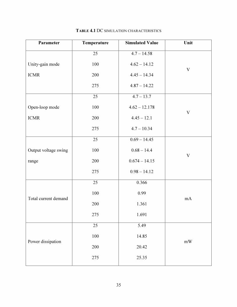
TABLE 4.1 DC SIMULATION CHARACTERISTICS
Parameter Temperature Simulated Value Unit
Unity-gain mode
ICMR
25
100
200
275
4.7 – 14.58
4.62 – 14.12
4.45 – 14.34
4.87 – 14.22
V
Open-loop mode
ICMR
25
100
200
275
4.7 – 13.7
4.62 – 12.178
4.45 – 12.1
4.7 – 10.34
V
Output voltage swing
range
25
100
200
275
0.69 – 14.45
0.68 – 14.4
0.674 – 14.15
0.98 – 14.12
V
Total current demand
25
100
200
275
0.366
0.99
1.361
1.691
mA
Power dissipation
25
100
200
275
5.49
14.85
20.42
25.35
mW

36
4.3 AC Simulation
AC simulation was used to characterize the following specifications: the open-loop gain,
unity-gain bandwidth (GB) and phase margin. All of these characteristics were measured using a
single test bench. The Fig. 4.3.1 shows the test bench setup for AC performance analysis. The
unity-gain bandwidth is furthermore verified in transient simulations.
Fig. 4.3.1. Test bench setup for AC analysis.
The open-loop gain of the op amp is limited by the bandwidth of the amplifier. There is a
tradeoff between the phase margin and the GB. To increase the phase margin, the GB and AC
gain will decrease and if we increase the GB and AC gain, the system will become less stable.
In the TABLE 4.2 the AC simulated parameters for 25 °C, 100 °C, 200 °C and 275 °C has
been presented. The simulations were executed using BSIM3 models. The simulations were run
again using an updated BSIM4 model that was developed after the fabrication.
37
TABLE 4.2 AC SIMULATION CHARACTERISTICS
Parameter
Temperature
(°C)
Simulated Value
Unit
Typical Fast-Fast Slow-Slow
Open loop
gain
25
100
200
275
74.29
66.32
65.81
60.84
59.6
52.5
36.11
42.51
73.03
63.67
57.23
57.18
dB
Unity-gain
Bandwidth
25
100
200
275
2.953
5.895
5.985
6.224
7.03
9.487
9.221
9.954
2.164
4.216
5.747
6.556
MHz
Phase Margin
25
100
200
275
40.65
42.93
45.11
42.1
36.4
36.1
50.8
50.1
38.4
40.6
41.5
41
(degree)
Fig. 4.3.2 and Fig. 4.3.3 represent the magnitude and phase plots for different temperatures
using the BSIM3 model. But in the updated BSIM4 device model, some of the circuit
performance declined: by 9% to 19% for open loop gain and 36% to 38% for phase margin;
while some performances improved: by 40% to 55% for unity-gain bandwidth.

38
Fig. 4.3.2 Magnitude plot for different temperatures.
Fig. 4.3.3 Phase plot for different temperatures.
-20
-10
0
10
20
30
40
50
60
70
80
1.00E+00 1.00E+01 1.00E+02 1.00E+03 1.00E+04 1.00E+05 1.00E+06 1.00E+07
Gain
(d
B)
Frequency (Hz)
Magnitude plot for different temperatures
25 °C
100 °C
200 °C
275 °C
-40
-20
0
20
40
60
80
100
120
140
160
180
200
1.00E+00 1.00E+01 1.00E+02 1.00E+03 1.00E+04 1.00E+05 1.00E+06 1.00E+07
Ph
ase
( °
C)
Frequency (Hz)
Phase plot for different temperatures
25 °C
100 °C
200 °C
275 °C

39
4.4 Transient Simulation
Transient simulation was used to characterize the following specifications: the closed-loop
unity-gain bandwidth and the slew rate. The test bench setup for the transient analysis is shown
in Fig. 4.4.1.
Fig. 4.4.1 Test bench for transient analysis.
To determine the closed-loop unity-gain bandwidth, the circuit was simulated with an
external feedback path. The amplitude of the ac signal was 10 mVp-p and the initial frequency
was 10 kHz. After this the frequency has been sweep until the output signal equals to input
signal. This frequency is the unity-gain bandwidth. The closed-loop unity-gain bandwidth for 25
°C is 2.6 MHz and the closed-loop unity-gain bandwidth for 275 °C is 7.2 MHz.
For the slew rate measurement the sinusoidal source is replaced by a pulse generator and the
feedback resistor replaced with a short. The frequency of the pulse signal was 10 kHz, the rise
and fall time are 5 ns each and the pulse width is 50 µs. The modified test bench for slew rate is
shown below in Fig. 4.4.2.
40
Fig. 4.4.2. Test bench for analysis of slew rate.
The slew rate is the fastest rate of change of the output voltage in response to a change of the
input voltage. It is expressed as volts per microsecond. Table 4.3 shows the simulated results of
the slew rate characteristics. For a fixed load capacitance of 10 pF, the supply current rises with
temperature due to the shift in threshold voltages. For this the slew rate also increases with
temperature. At all temperatures the simulated slew rate is higher than the SR specification of 10
V/µs.
TABLE 4.3 AC SLEW RATE VALUE FOR DIFFERENT TEMPERATURES
Temperature ( °C) Vmax (V) Vmin (V) Slew rate (V/µs)
25
100
200
275
14.6
14.27
14.33
14.45
0.066
0.056
0.27
0.35
26.41
71.35
76.6
95.88

41
CHAPTER 5
PHYSICAL DESIGN
The last step in the design process is the physical design or the layout. The toolchain for the
layout is the Virtuoso Layout Editor in the Cadence design kit. The complete layout process
includes the layout of the transistors with proper connections, the pin specification, the design
rule check verifications and layout vs schematic check. After the layout, the op amp is placed
inside the padframe and parametric extraction performed. Finally, the circuit is resimulated with
the padframe to confirm the performance characteristics.
5.1 Chip Layout
The chip layout is divided into two stages: the differential input stage and the common
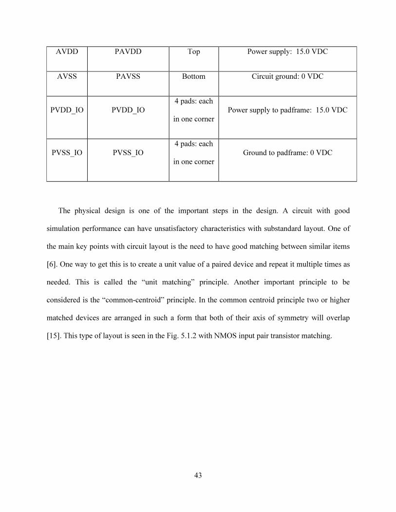
source amplifier output stage. There are a total of eight pins associated with the layout: AVDD
and AVSS for power supplies, VINP and VINN for positive and negative inputs, respectively,
VBIAS for voltage biasing, PVDD_IO and PVSS_IO for power supplies to padframe and
OUTPUT for the output. The Fig. 5.1.1 represents the layout of the op amp and the Table 5.1
represents the input and output pins of op amp and their description.

42
Fig. 5.1.1. The layout of the op amp (Length = 431.6 µm; Width = 738 µm).
TABLE 5.1 THE INPUT AND OUTPUT PINS OF OP AMP WITH DESCRIPTION
Pin Name Pad Frame Name Location Connection Description
VINP POTA2STG_VINP Upper-left Positive Input: 7.5 V DC + 1 V AC
VINN POTA2STG_VINN left Negative Input: 7.5 V DC voltage
VBIAS POTA2STG_VBIAS Lower-Left Desired Biasing Voltage: 4.45 V DC
OUTPUT POTA2STG_OUTPUT Right Output
43
AVDD PAVDD Top Power supply: 15.0 VDC
AVSS PAVSS Bottom Circuit ground: 0 VDC
PVDD_IO PVDD_IO
4 pads: each
in one corner
Power supply to padframe: 15.0 VDC
PVSS_IO PVSS_IO
4 pads: each
in one corner
Ground to padframe: 0 VDC
The physical design is one of the important steps in the design. A circuit with good
simulation performance can have unsatisfactory characteristics with substandard layout. One of
the main key points with circuit layout is the need to have good matching between similar items
[6]. One way to get this is to create a unit value of a paired device and repeat it multiple times as
needed. This is called the “unit matching” principle. Another important principle to be
considered is the “common-centroid” principle. In the common centroid principle two or higher
matched devices are arranged in such a form that both of their axis of symmetry will overlap
[15]. This type of layout is seen in the Fig. 5.1.2 with NMOS input pair transistor matching.
44
Fig. 5.1.2. NMOS input pair transistor matching.
The layout structure implements “inter-digitated arrays” or in other words, uses a single
multi-fingered transistor to represent two or more transistors. The current mirror load of the
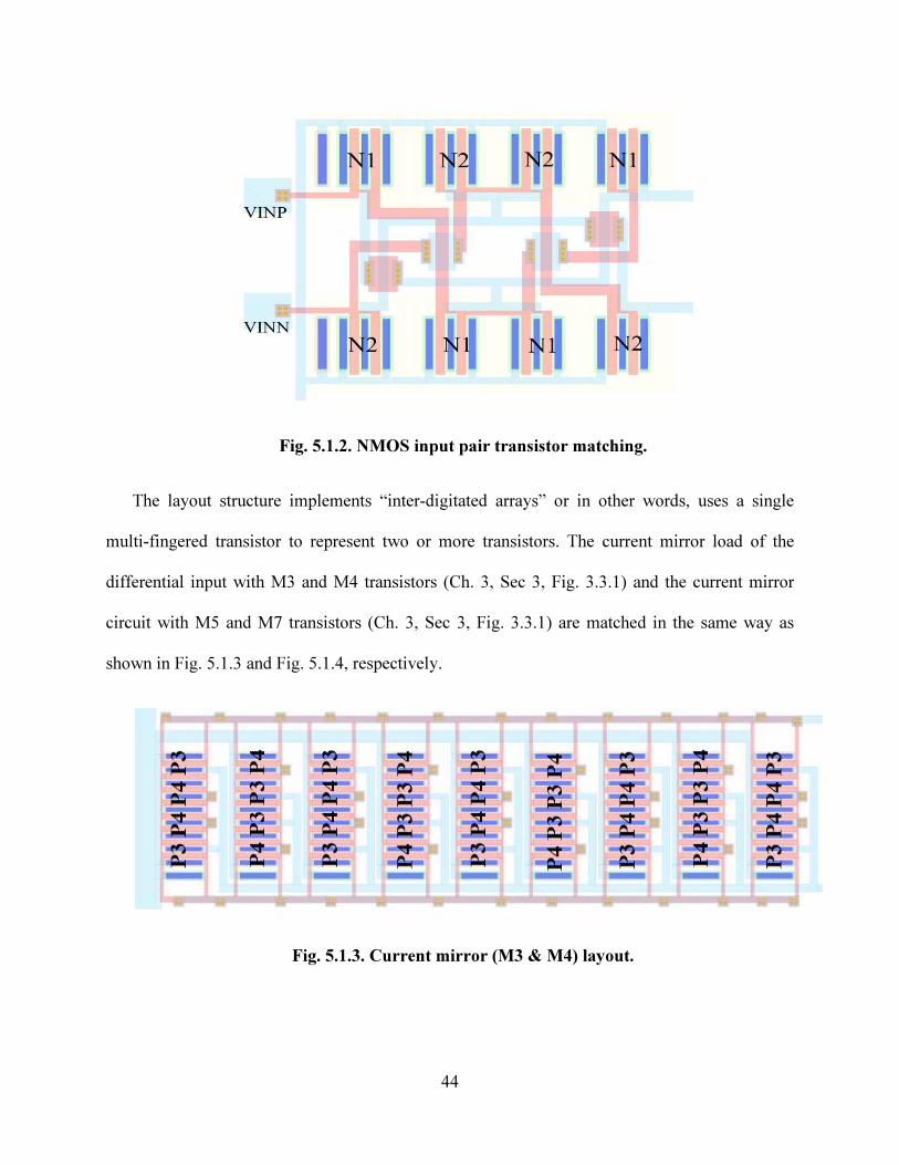
differential input with M3 and M4 transistors (Ch. 3, Sec 3, Fig. 3.3.1) and the current mirror
circuit with M5 and M7 transistors (Ch. 3, Sec 3, Fig. 3.3.1) are matched in the same way as
shown in Fig. 5.1.3 and Fig. 5.1.4, respectively.
Fig. 5.1.3. Current mirror (M3 & M4) layout.

45
Fig. 5.1.4. Current mirror (M5 & M7) layout.
The transistor-matching layout of the op amp follows the layout rules for common-centroid
layout design according to [15]. The rules are given below:
1. Coincidence: The placement of the matching transistors maintains the coincidence of
their centroids.
2. Symmetry: The device array is symmetric in both X- and Y-axes.
3. Dispersion: The device segments are uniformly distributed
4. Compactness: The device is compacted as much as possible following the device rules.
A number of contacts are placed and large paths of the poly layer have been superimposed
with metal layer to provide minimum resistance path. A large number of contacts have been
placed in these paths as well.

46
The design rules check was performed throughout the layout process and layout versus
schematic was used to confirm the proper connections in the device. Next, parasitic extraction of
the op amp was performed and the actual parasitic capacitance and resistance values from the
layout extracted. The op amp was resimulated with these extracted values to confirm its
performance.
The final layout includes the padframe with eight analog pads for proper bond wiring,
packaging and testing. The final layout with padframe and inputs & output bondpads is shown in
Fig. 5.1.5 below.
Fig. 5.1.5. Final chip layout with padframe and pin connections.
VINP
VINN
VBIAS
OUTPUT
AVDD
AVSS
PVSS_IO
PVSS_IO PVDD_IO
PVDD_IO

47
The full chip included over 40 analog, mixed-signal and digital building block circuits. The
final chip size was 21 x 12.5 mm2 and the chip was sent to fabrication on August 2013. The final
area of the op amp including the padframe is 1200 µm X 1520 µm and the final circuit includes a
total of seven transistors and one capacitor and one resistor. The die micrograph of the fabricated
op amp is shown in Fig. 5.1.6.
Fig. 5.1.6. Die micrograph of the fabricated op amp.

48
CHAPTER 6
TESTING AND CHARACTERIZATION
After the tapeout the die was sent for fabrication. Testing preparations such as test planning
and packaging options were evaluated during this time. Since the main application of the circuit
is in high temperature different bonding and packaging options that were compatible with the
temperature range were considered. A detailed test plan was developed and printed circuit board
created to reproduce the test benches used at the design and verification steps.
6.1 Bond Wire and Packaging
Due to the low pin count of the circuit, testing using a Semiprobe probe station was the
primary choice. Exhaustive DC testing was performed using the probe station and Keithley 4200
Semiconductor Characterization System. But to measure the op amp transient performance in
feedback circuitry packaging of the circuit was required.
The packaging and wire bonding was accomplished at the High Density Electronics Center
(HiDEC) at the University of Arkansas. The first step was dicing of the op amp reticle from the
fabricated 4” wafers. After this step, the die was attached into the cavity of a 64-pin ceramic
quadpack package using high-temperature epoxy and the package was kept inside a vacuum
oven for about 4 hours at 150 °C to cure the epoxy. The next step was wire bonding. The pads of
the circuit were bonded to the package by using a 1 mil gold wire with a small gold ball formed
by the bonder at the ends. The bonding plan for the op amp is shown in the Fig. 6.1.1 below.

49
Three op amps (along with one other circuit, a Schmitt trigger designed by a fellow student)
were bonded in a single package. The pin out information is detailed in TABLE 6.1.
Fig. 6.1.1. Bonding plan.
TABLE 6.1 THE BONDING DIAGRAM PIN CONFIGURATIONS
Pin No.
Corresponding
Signal
Pin No.
Corresponding
Signal
Pin No.
Corresponding
Signal
10 PAVDD 26 PAVDD 42 PAVDD
12 VINP 28 VINP 44 VINP
14 VINN 30 VINN 46 VINN
16 VBIAS 32 VBIAS 48 VBIAS
17 PVDD_IO 33 PVDD_IO 49 PVDD_IO
19 PAVSS 35 PAVSS 51 PAVSS
21 PVSS_IO 37 PVSS_IO 53 PVSS_IO
23 Output 39 Output 55 Output
50
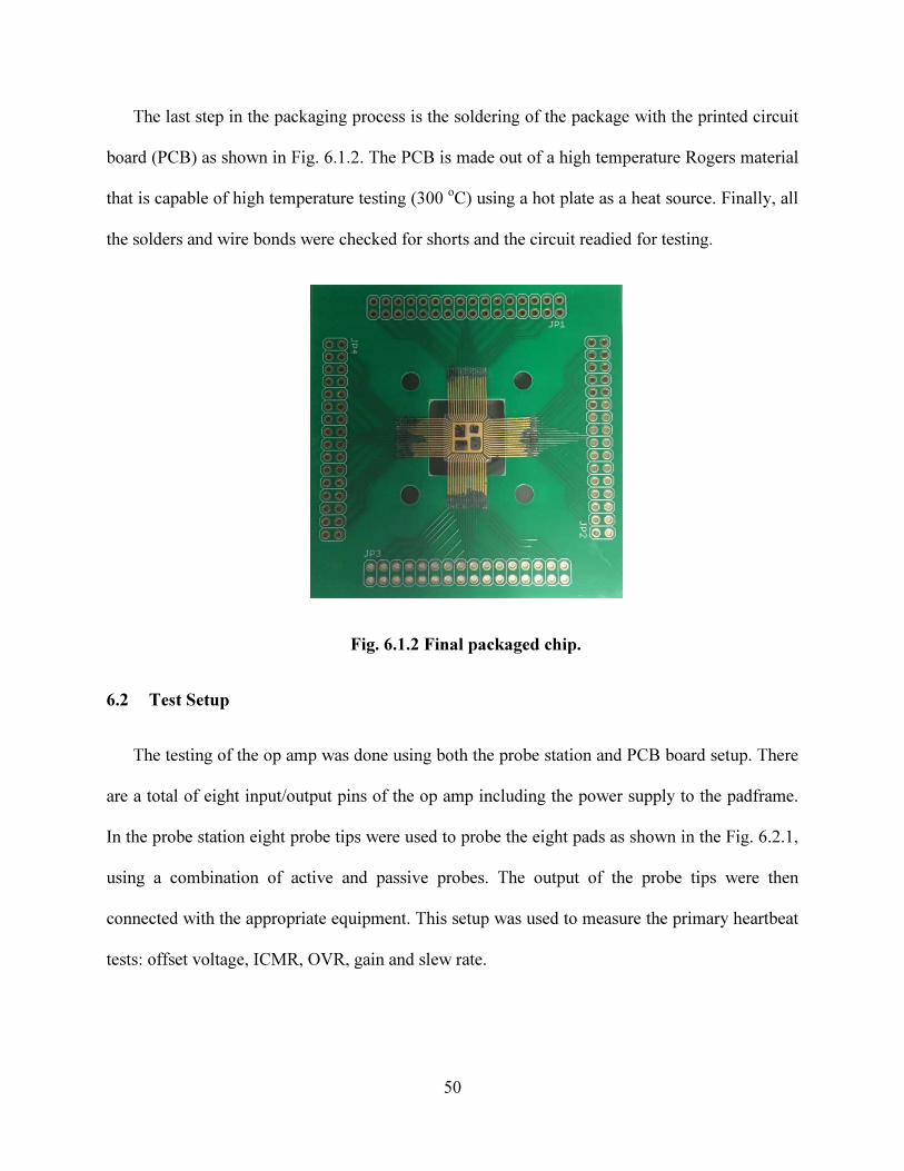
The last step in the packaging process is the soldering of the package with the printed circuit
board (PCB) as shown in Fig. 6.1.2. The PCB is made out of a high temperature Rogers material
that is capable of high temperature testing (300 oC) using a hot plate as a heat source. Finally, all
the solders and wire bonds were checked for shorts and the circuit readied for testing.
Fig. 6.1.2 Final packaged chip.
6.2 Test Setup
The testing of the op amp was done using both the probe station and PCB board setup. There
are a total of eight input/output pins of the op amp including the power supply to the padframe.
In the probe station eight probe tips were used to probe the eight pads as shown in the Fig. 6.2.1,
using a combination of active and passive probes. The output of the probe tips were then
connected with the appropriate equipment. This setup was used to measure the primary heartbeat
tests: offset voltage, ICMR, OVR, gain and slew rate.

During the testing of the op amp using
setup were kept in two different PCB using a mother
connections were made between them. This
where the packaged chip Rogers board placed in the hot plate is capable to withstand high
temperature but not vice versa. Two test boards, one 1.5 inch x 2.5 inch and another 1.45 inch
1.55 inch were developed using Eaglesoft PCB software as shown in
The list of equipment used for testing is represented in
for each characteristic measurement
Appendix A.
51
Fig. 6.2.1 Probe station test setup.
During the testing of the op amp using the PCB board setup, the packaged chip and the test
kept in two different PCB using a mother-daughter board setup and external
etween them. This was been done to facilitate high temperature testing
where the packaged chip Rogers board placed in the hot plate is capable to withstand high
temperature but not vice versa. Two test boards, one 1.5 inch x 2.5 inch and another 1.45 inch
1.55 inch were developed using Eaglesoft PCB software as shown in Fig. 6.2.2.
The list of equipment used for testing is represented in TABLE 6.2. The test plan developed
measurement along with the diagrams and connections are included in
he packaged chip and the test
daughter board setup and external
been done to facilitate high temperature testing
where the packaged chip Rogers board placed in the hot plate is capable to withstand high
temperature but not vice versa. Two test boards, one 1.5 inch x 2.5 inch and another 1.45 inch x
. The test plan developed
along with the diagrams and connections are included in
52
TABLE 6.2 LIST OF TEST EQUIPMENT
Tektronix TDS 744A Oscilloscope
Tektronix AFG3022B Dual Channel Arbitrary/ Function Generator 25MHz
Agilent E3631A Triple Output DC Power Supply
Keithley Semiconductor Characterization System
Hewlett Packard 3458A Multimeter
Cole Parmer Stable Temp hotplate
Marconi Instrument 10KHz, 2.7GHz signal Generator 2031
Printed Circuit Board
Fig. 6.2.2. PCB layout (a) 1.45” x 1.55” (b) 1.5” x 2.5”.

6.3 Test Results
This section describes the actual performance of the designed circuit at different temperature
ranges. The first test performed was
test was to observe that the circuit
been tested sporadically to check for functionality and the device yield was 100% although the
dies in the edge of the wafer showed better transient performance than dies in the center due to
their stronger PMOS and weaker
where the shaded dies represent the tested circuits.
Once functional circuits were identified, t
the optimum bias voltage (the same range as the simulation
53
This section describes the actual performance of the designed circuit at different temperature
. The first test performed was a “heartbeat” test at the probe station. The purpose of this
observe that the circuit was functional. Die from different location of the wafer ha
been tested sporadically to check for functionality and the device yield was 100% although the
dies in the edge of the wafer showed better transient performance than dies in the center due to
weaker NMOS properties. The Fig. 6.3.1 shows the wafer diagram
where the shaded dies represent the tested circuits.
Fig. 6.3.1 Wafer diagram
Once functional circuits were identified, the next test performed was a bias sweep to measure
he same range as the simulation Fig. 6.3.2). The input was provided
This section describes the actual performance of the designed circuit at different temperature
The purpose of this
Die from different location of the wafer has
been tested sporadically to check for functionality and the device yield was 100% although the
dies in the edge of the wafer showed better transient performance than dies in the center due to
shows the wafer diagram
bias sweep to measure
. The input was provided
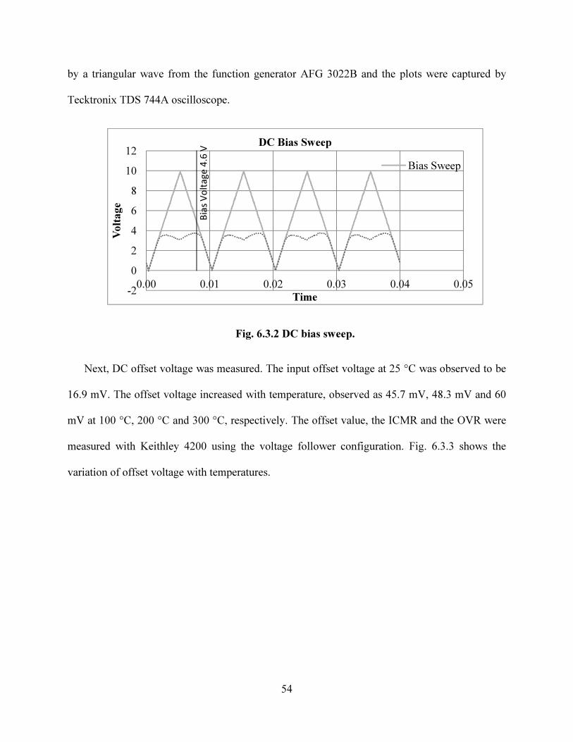
54
by a triangular wave from the function generator AFG 3022B and the plots were captured by
Tecktronix TDS 744A oscilloscope.
Fig. 6.3.2 DC bias sweep.
Next, DC offset voltage was measured. The input offset voltage at 25 °C was observed to be
16.9 mV. The offset voltage increased with temperature, observed as 45.7 mV, 48.3 mV and 60
mV at 100 °C, 200 °C and 300 °C, respectively. The offset value, the ICMR and the OVR were
measured with Keithley 4200 using the voltage follower configuration. Fig. 6.3.3 shows the
variation of offset voltage with temperatures.
-2
0
2
4
6
8
10
12
0.00 0.01 0.02 0.03 0.04 0.05
Volt
age
Time
DC Bias Sweep
Bias Sweep
Bia
s V
olt
ag
e 4
.6 V

55
Fig. 6.3.3. The offset voltage at different temperatures
The measured unity-gain mode ICMR, OVR and DC current supply at 25 °C are shown in
Fig. 6.3.4.
Fig. 6.3.4. Input common mode range at 25 °C.
The measured unity-gain mode ICMR, OVR and DC current supply at 300 °C is shown in
Fig. 6.3.5.
0
10
20
30
40
50
60
70
0 50 100 150 200 250 300 350
Volt
age
(mV
)
Temperature (°C)
Offset Voltage
Offset Voltage
7.50E-06
1.25E-05
1.75E-05
2.25E-05
2.75E-05
0.00
2.00
4.00
6.00
8.00
10.00
12.00
14.00
16.00
0.00 5.00 10.00 15.00
Vou
t (V
)
Vin (V)
Unity-gain mode ICMR at 25 °C
For 25 °C Vout
For 25 °C I_supply
I_su
pp
ly (
A)

56
Fig. 6.3.5 Input common mode range at 300 °C.
The unity-gain mode ICMR is 5.85 V to 14.03 V at 25 °C and 5.25 V to 11.8 V at 300 °C.
For all temperatures the ICMR range is smaller than simulated values. This is due to the fact that
the actual threshold voltages of the transistors are higher than the device model. The OVR is 1.73
V to 14 V at 25 °C and 0.53 V to 11.2 V at 300 °C. The OVR is also smaller than the simulated
values due to the same reason. The current consumption and power dissipation at 25 °C is 6.2
mA and 93 mW respectively, and at 300 °C is 18.8 mA and 282 mW respectively. The measured
current consumption and power dissipation is higher than simulation due to the fact that a larger
bias voltage was required to make sure all of the transistors were in saturation. The summary of
the results at different temperature is shown in TABLE 6.3.
-5.00E-03
0.00E+00
5.00E-03
1.00E-02
1.50E-02
2.00E-02
2.50E-02
0.00
2.00
4.00
6.00
8.00
10.00
12.00
14.00
0.00 5.00 10.00 15.00
Vou
t (V
)
Vin (V)
Unity-gain mode ICMR at 300 °C
For 300 °C Vout
For 300 °C I_supply
I_su
pp
ly (
A)

57
TABLE 6.3 OP AMP DC CHARACTERISTICS MEASUREMENTS
Parameter Temperature Simulated Value Measured Value Unit
Offset voltage
25
100
200
275/300*
---
---
---
---
16.9
45.7
48.3
60
mV
Unity-gain ICMR
25
100
200
275/300*
4.7 – 14.58
4.62 – 14.12
4.45 – 14.34
4.87 – 14.22
5.85 – 14.03
5.6 – 13.1
5.3 – 12.2
5.25 – 11.8
V
Output voltage swing
range
25
100
200
275/300*
0.69 – 14.45
0.68 – 14.4
0.674 – 14.15
0.98 – 14.12
1.73 – 14
1.37 – 12.8
0.53 – 11.6
0.53 – 11.2
V
Total current
consumption
25
100
200
275/300*
0.366
0.99
1.361
1.691
6.2
11.94
15.7
18.8
mA
Power dissipation
25
100
200
275/300*
5.49
14.85
20.42
25.35
93
179
235.5
282
mW
*Simulation/Measurement

58
Next, transient analysis was performed and a speculation on slew rate and unity-gain
bandwidth was measured in Fig. 6.3.6. For the slew rate measurement, a 2 Vp-p (6.5 V to 8.5 V)
square wave signal was provided to the positive input of the OTA from the function generator
AFG 3022B and the plots were captured by Tecktronix TDS 744A. The specification of the load
capacitance in the output was on the order of a few pF (≈10 pF). The output pad was probed
using a passive probe. The probe was connected to the oscilloscope through a 4.5 ft RG-174
coaxial cable followed by a 3 ft. RG-58 coaxial cable. The minimum capacitance of the RG-174
is 30.8 pF/ft. [16] and the maximum capacitance of the RG-58 is 26 pF/ft. [17]. So the worst case
load capacitance is in the range of 200 pF. The measured slew rate at 25 °C is 13.34 V/µs and at
300 °C is 50 V/µs. The Fig. 6.3.6 shows the slew rate measurement at room temperature.
Fig. 6.3.6. Slew rate measurement at 25 °C.
The unity-gain bandwidth with active probe at room temperature is 1.8 MHz and at 300 °C is
6.1 MHz. The used Picoprobe model 12C active probe has 0.1 pF capacitance [18]. The unity-

59
gain bandwidth with passive probe at room temperature is 1 MHz and at 300 °C is 3.4 MHz.
Here with the passive probe at the output, the load is assumed at least 2 times higher than the
simulation load. So the unity-gain bandwidth measurements match with the simulation results.
The open loop voltage gain at 25 °C is 63 dB and at 300 °C is 57.5 dB. Although the open
loop voltage gain in every temperature is less than the simulation value using BSIM3 model but
they match with the simulation value using BSIM4 model. The BSIM4 model has a more
accurate frequency response and this model is more closely related with the real output. The Fig.
6.3.7 represents the open loop voltage gain at room temperature.
Fig. 6.3.7. DC gain measurement at 25 °C.
The summary of the op amp results at different temperature is shown in TABLE 6.4.
-2.00
0.00
2.00
4.00
6.00
8.00
10.00
12.00
14.00
16.00
7.10 7.11 7.12 7.13
Vou
t (V
)
VINP (V)
DC Gain at 25 °C
Vout
63 dB
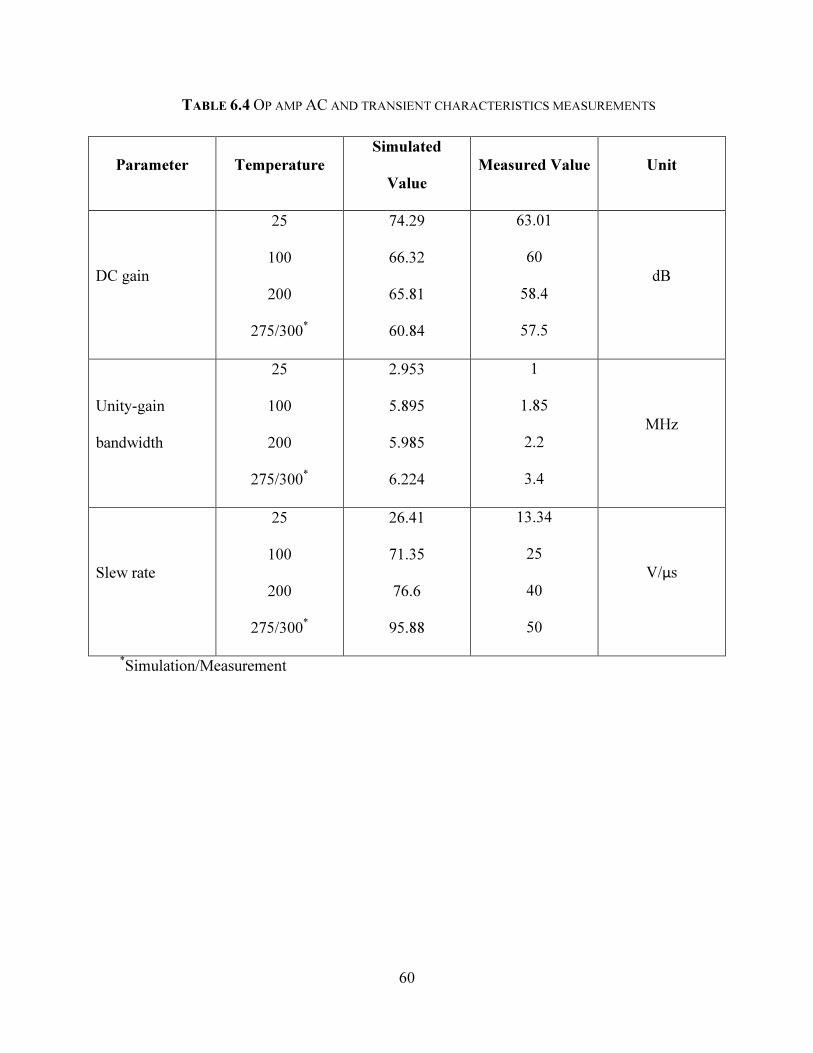
60
TABLE 6.4 OP AMP AC AND TRANSIENT CHARACTERISTICS MEASUREMENTS
Parameter Temperature
Simulated
Value
Measured Value Unit
DC gain
25
100
200
275/300*
74.29
66.32
65.81
60.84
63.01
60
58.4
57.5
dB
Unity-gain
bandwidth
25
100
200
275/300*
2.953
5.895
5.985
6.224
1
1.85
2.2
3.4
MHz
Slew rate
25
100
200
275/300*
26.41
71.35
76.6
95.88
13.34
25
40
50
V/µs
*Simulation/Measurement

61
CHAPTER 7
CONCLUSION
This thesis has presented the overall design flow of a general purpose two-stage CMOS op
amp using SiC CMOS process technology. The designed circuit is one of the pioneering op amp
in SiC CMOS technology designed to operate in high temperature range and harsh environment.
The purpose of the overall project was to build individual circuit blocks that would be further
integrated into a system level design in the next tapeout of NSF-BIC project. An improved
version of the designed amplifier has become part of the design of the protection circuitry of a
SiC gate driver system that has subsequently been submitted for fabrication.
From the beginning, the main consideration was to design a circuit that would function with
good performance characteristics. The pin count has been kept small to simplify testing using
both board and probe station methods. This reduced both the time and money required over
packaging of random die prior to validation.
The op amp is functional over a wide temperature range and has good performance
characteristics. The DC gain of the op amp ranges from 63 dB to 57 dB over temperature (25 °C
to 300 °C ) and the unity-gain bandwidth ranges from 1 MHz to 3.4 MHz over temperature (25
°C to 300 °C ). The op amp shows slew rate from 13.34 V/µs to 50 V/µs over the temperature
range. The circuit has high power dissipation: ranging from 93 mW to 282 mW. But for the SiC
CMOS process with high threshold voltages ranging from 2.9 V to 5 V with 15 V supply voltage

62
this power consumption rate is acceptable. The simulations were performed based on BSIM3
models developed for the particular process. The experimental results matches better with the
simulation results for the BSIM4 model that developed after the fabrications.
Future Work
Another version of the op amp has been developed and submitted for fabrication in a
subsequent run. The simulation of this new three-stage op amp shows good results, but the
experimental results still need to confirm functionality. The second version of the op amp needs
to be tested using the developed testplan.

63
REFERENCES
[1] J. Mahattanakul, "Design Procedure for Two-Stage CMOS Opamp With Flexible Noise-
Power Balancing Scheme," CIRCUITS AND SYSTEMS—I: REGULAR PAPERS, vol. 52,
no. 8, pp. 1508-1514, 2005.
[2] A. Vert, Z. Shen and R. Normann, "Silicon Carbide High Temperature Operational
Amplifier," in IMAPS High Temperature Electronics , Albuquerque, 2012.
[3] A. Francis, A. Rahman, J. Holmes, P. Shepherd, S. Ahmed, M. Barlow, S. Bhuyan, L.
Caley, T. Moudy, H. A. Mantooth and J. Di, "Design of Analog and Mixed-Signal
Integrated SiC CMOS Circuits with a High Fidelity Process Design Kit," in Government
Microcircuit Applications & Critical Technology Conference, Charleston , 2014.
[4] B. Razavi, Design of Analog CMOS Integrated Circuits, New York: McGraw-Hill, 2001.
[5] A. Sedra and K. Smith, Microelectronic Circuits Theory and Applications, New Delhi:
Oxford University Press, 2009.
[6] D. R. H. Phillip E. Allen, CMOS Analog Circuit Design, 3rd ed., New York: Oxford
University Press, Inc., 2012.
[7] W. Jung, "Op Amp Applications Handbook," Newnes Elsevier , Oxford, 2005.
[8] B. Al-Hashimi, J. Fidler and P. Garner, "High Frequency Active Filters using OTAs," in
Electronic Filters, IEE Colloquium, London, 1989.
[9] R. J. Baker, CMOS Circuit Design, Layout, and Simulation, New Jersey: John Wiley &
Sons, Inc. , 2010.
[10] Y. Zhen, "Current Sensing Circuit Concepts and Fundamentals," Microchip Technology
Inc., 2010-2011.
[11] R. Thompson, D. Clark, A. Murphy, A. Ramsay, D. Smith, R. Young, J. Cormack, J.
McGonigal, J. Fletcher, C. Zhu, S. Finney, L. Martin and A. Horsfall, "High Temperature
Silicon Carbide CMS Integrated Circuits," in International Microelectronics Assembly and
Packaging Society , Oxford, 2011.
64
[12] F. Amroso, A. Pugliese and G. Cappuccino, "Design Considerations for Fast Settling Two-
Stage Miller-Compensated Operational Amplifiers," in Electronics, Circuits, and Systems,
2009.
[13] J. Jung, A. Huang and Z. Du, "Simulated Performance of SiC Based OP-AMP at High
Temperature," in Power Electronics Specialists Conference, 2006.
[14] A. Gupta, D. Mishra, R. Khatri, U. Chandrawat and P. Jain, "A Two Stage and Three Stage
CMOS OPAMP with Fast Settling, High DC Gain and Low Power Designed in 180nm
Technology," in Computer Information Systems and Industrial Management Applications ,
2010.
[15] A. Hastings, The Art of Analog Layout, New Jersey: Prentice Hall, 2001.
[16] General Cable, Product data sheet for part number C1156 (RG 174/U type coaxial cable),
2011.
[17] West Penn Wire, Technical data sheet for RG58 coaxial 50 Ohm cable (Part Number 813),
2010.
[18] GGB Industries Inc., Picoprobe Model 12C.
65
APPENDIX – A
OP AMP TEST PLAN
A. General Power-up Procedure
1. Start with connecting the AVDD and PVDD_IO to +15 V and AVSS and PVSS_IO to
common ground 0V to the PCB.
2. Set VBIAS to the desired +4.45V voltage.
3. Depending on the test, place the VINN and VINP connection in the respective AC or DC
voltage.
4. Set the power supplies then press the “output off” button.
5. Recheck carefully every voltage of the pins.
6. Wire the pins of the chip in Rogers board with the PCB.
7. Proceed with the test.
8. Measure the results and record the data.
9. After finishing the testing turn of the input signals followed by the bias voltages and
power supplies.

66
B. High Temperature General Procedure
1. Continue the general power-up procedure from step 1 to 5.
2. Attach the Roger board in the high temp settings and place it in the hot plate.
3. Turn on the hot plate and set the required temperature for individual testing.
4. Continue on the general power-up steps from 6 to 9.
5. Cool down the chip to room temperature.
C. DC Characterization
DC Offset
1. The DC offset measurement test bench is shown in Fig. A.C.1.
Fig. A.C.1. Input offset voltage measurement
2. Set up using the general power–up procedure.
3. Set VINN = VINP = 7.5 V

67
4. Measure Vout using the multimeter.
5. Determine the relation between the Buffer stage and the Device under test, using the
following equation:
∆ = −∆1 (A.1)
6. The offset voltage VOS can be calculated, using the following equation:
##$ ≈ 1000
(A.2)
7. Repeat the test with temperatures ranging from 25 o
C to 300oC.
8. Measure the results and record the offset voltage.
DC Power
1. Use the test bench as shown in Fig. A.C.1.
2. Set up using the general power–up procedure.
3. Set VINN = VINP = 7.5 V
4. Measure the DC current by connecting a multimeter in current mode in series with the
power supply. For safety add a 100 Ω resistor between the multimeter and power
supply.
5. Repeat the test with temperatures ranging from 25 o
C to 300oC.
6. Measure the results and record the data.
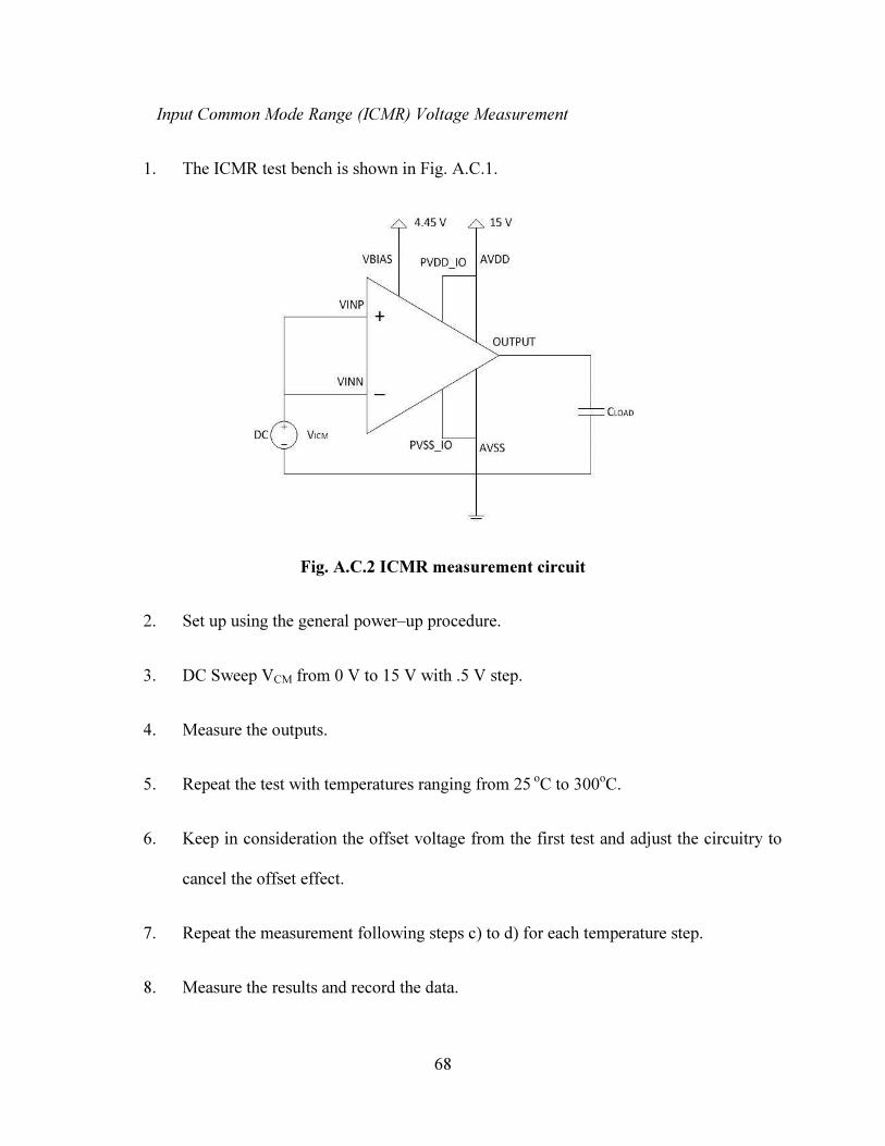
68
Input Common Mode Range (ICMR) Voltage Measurement
1. The ICMR test bench is shown in Fig. A.C.1.
Fig. A.C.2 ICMR measurement circuit
2. Set up using the general power–up procedure.
3. DC Sweep VCM from 0 V to 15 V with .5 V step.
4. Measure the outputs.
5. Repeat the test with temperatures ranging from 25 o
C to 300oC.
6. Keep in consideration the offset voltage from the first test and adjust the circuitry to
cancel the offset effect.
7. Repeat the measurement following steps c) to d) for each temperature step.
8. Measure the results and record the data.

69
D. AC Characterization
Open Loop Gain
1. The test bench for open loop voltage gain is shown in Fig. A.D.1.
Fig. A.D.1. Open loop gain test bench
2. Set up using the general power–up procedure.
3. Connect VMID to 7.5 V.
4. DC Sweep VSRC from 0V to 15V and measure Vout.
5. Calculate the open loop gain using the following equation:
: = 20 log '100Ω + 100KΩ
100Ω∗∆V%&'
∆Vout( (A.3)
7. Repeat the test with temperatures ranging from 25 o
C to 300oC.
6. Measure the results and record the data.

70
Unity-Gain Bandwidth
1. The test bench for unity-gain bandwidth is shown in Fig. A.D.2.
Fig. A.D.2. Test bench for power dissipation and unity gain bandwidth
2. Set up using the general power–up procedure.
3. From the arbitrary waveform generator set the sinusoidal input signal. Set the offset
value, the amplitude to 200 mVp-p, and the frequency to 10 kHz initially.
4. Connect VINN to 7.5 V.
5. Sweep the frequency from 1Hz to 10 MHz and measure the frequency for which the
input is equal to the output i.e. the output signal amplification is zero. This is the
unity-gain bandwidth.
6. Repeat the test with temperatures ranging from 25 o
C to 300oC.
7. Measure the results and record the data.

71
Common Mode Rejection Ratio (CMRR)
1. The test bench for CMRR is shown in Fig.A.D.3.
Fig.A.D.3. CMRR test bench
2. Set up using the general power–up procedure.
3. Connect VMID to 7.5 V.
4. Sweep VSRC from 0V to 15V and measure Vout.
5. Calculate the CMRR using the following equation:
= 20log ' 100;100; + 1008; ∗
∆∆( ( (A.4)
6. Repeat the test with temperatures ranging from 25 o
C to 300oC.
7. Measure the results and record the data

72
Power Supply Rejection Ratio (PSRR)
1. The test bench for PSRR is shown in Fig. A.D.4
Fig. A.D.4. PSRR test bench
2. Set up using the general power–up procedure.
3. From the arbitrary waveform generator set the sinusoidal input signal. Set the offset
value, the amplitude to 200 mVp-p, and the frequency to 10 kHz initially.
4. Connect VINN to 7.5 V.
5. Sweep the frequency from 1Hz to 10MHz and measure the differential output.
6. Calculate the PSRR using the following equation:
= 20 log $VACVout
X10% (A.5)
7. Repeat the test with temperatures ranging from 25 o
C to 300oC.
8. Measure the results and record the data.
10 KΩ

73
E. Transient Characterization
Slew Rate
1. The test bench for slew rate is shown in Fig. A.E.1
Fig. A.E.1. Slew rate test bench
2. Set up using the general power–up procedure.
3. From the arbitrary waveform generator set the input square signal. Set the offset
value, the amplitude to 2 Vp-p, and the frequency to 10 kHz initially.
4. Connect VINN to 7.5 V.
5. Calculate the slope of the rising and falling edge. This is the value of the slew rate.
6. Repeat the test with temperatures ranging from 25 o
C to 300oC.
7. Measure the results and record the data.

74
APPENDIX – B
DESIGN OF AN OP AMP IN THE SUBSEQUENT RUN
The designed and tested op amp has been re-designed in the next fabrication run. The op amp
in the run 1 shows instability in the updated BSIM4 model. In this model the circuit performance
such as the gain and the phase margin declined: by 9% to 19% for open loop gain and 36% to
38% for phase margin. The range of the phase margin is from 28° to 21°. For this the op amp was
unstable. Also special consideration was required for the voltage source bias input. The circuit
could be over biased or under biased for a fixed DC bias voltage in different temperatures. Also
the threshold voltage of the transistors will also shift due to the voltage biasing.
A more stable op amp with current bias input has been designed in the next run. The
schematic of the circuit is shown in the Fig. B.1 below.
Fig. B.1. Three stage op amp schematics.

75
This op amp has an added third stage. The third stage is a common source amplifier
employed to increase the gain. The increased gain has been traded for the better phase margin.
The third stage will introduce more poles and for this another compensation circuit has been
added in the op amp. This compensation circuit also consists of a Miller compensation capacitor
connected in series with a nulling resistor. The phase margin of the op amp has been improved
with the cost of the gain.