design of a distributed clock generator for multiple power
TRANSCRIPT

Master Thesis
October 2008
Design of a Distributed Clock Generator for Multiple Power Domain System-on-Chip Integrated Circuits
Msc. student: Jinbo Wan Mentor at NXP Semiconductors: Maurice Meijer,
Arnoud van der Wel Supervisor at TUDelft: Prof. John Long

Abstact
2
Abstract
Modern system-on-chip IC designs show great requirement on minimizing power con-
sumptions. One of the low power techniques is using dynamic voltage frequency scaling
for each power domain. Yet the clock generator unit is the bottleneck to apply this
technique. In this thesis, we focus on the local clock generator unit solution and design
three new local clock generators which share the power supply with digital blocks. The
best candidate provides good jitter performance (10ps) under large power supply noise,
low power consumption (900µW) and small area (90×60µm2). The influence of power
supply noise on jitter of each circuit components, like voltage control oscillator, fre-
quency divider, phase frequency detector, charge pump, loop filter and clock buffers are
studied in thoroughly.

Acknowledgments
3
Acknowledgments
First of all, I wish to show my great thanks to my supervisor in NXP company, Maurice
Meyer. He is patient, kind and can always give me the correct direction and support in
my study. Some time when I went far away from the red line, and deep into some points
which may only improve 1% of the system, Maurice can always give me remind and
drag me back. In the thesis writing time, he spent a lot of time to help me modify my
thesis and gave me a lot of good advices. Here I also want to show my apologize to
Maurice for some sudden disappears of me during the project study. And I can never
forget the BBQ party in Maurice home.
Another important person for my study is Prof. John Long in TUDelft. He is my super-
visor in the university. Although John went to meet me just once a month, he always
kept in tight concern with my project, and gave me a lot of valuable help in my study. In
fact when I review the project study now, I can find that some of his advices are hit the
nail on the head. During my thesis writing, John also spent a lot of time to help me
improve the thesis and give a lot of good comments. If possible, I hope I can doing a
PhD study under his instruction.
I wish to thank Arnoud Van Der Wel in NXP company. He is my anolog rule No.1, and
give me many great helps on the anolog circuits design and layout. During the theory
study period, he help me a lot in demonstrate the suitable project solutions. I also wish
to thank Nenad Pavlovic in the NXP company. He help me to solve the PLL problems
and give me many valuable advices on my PLL designs. In fact, it’s he who explain to
me how Cadence do in calculation the phase noise and jitter of the oscillator, and made
me understand deeply in such fields.
Whithout Leo Warmerdam and Wouter Lintsen, I can’t carry out the project in NXP
company. Here I wish to own my great thanks to them for providing such a good chance
for met.
There are still many peoples who give me kind help during my project study, like
wendy.smit who help me to repair my computer and Desiree E M Janssen who help me
to solve the financial problem in the NXP. I can’t remember all of the name. But I wish
to show my best wishes to them. Thanks for all of you!

Table of Contents
4
Table of Contents
1. Introduction............................................................................................................ 13
1.1. Clock Generation in Modern System Chips................................................... 13
1.2. Project Description......................................................................................... 15
1.3. Report Outline ................................................................................................ 15
Reference ................................................................................................................. 16
2. SoC Clock Generation Approach......................................................................... 17
2.1. Clocking Requirements for Digital Logic Blocks.......................................... 17
2.2. Review of the Central Clocking Approach .................................................... 19
2.3. Review of the Local Clocking Approach....................................................... 21
2.4. Inter Power Domain Communication Schemes for L-CGU .......................... 23
2.5. L-CGU Requirements and Design Specifications.......................................... 24
2.6. Summary ........................................................................................................ 25
Reference ................................................................................................................. 26
3. Jitter Performance Models ................................................................................... 27
3.1. Jitter Definitions............................................................................................. 27
3.2. Phase noise ..................................................................................................... 29
3.2.1. ( )ovS f : Passband spectrum of the oscillator signal ( )ov t ................. 30
3.2.2. ( )L f∆ : Single Side Band (SSB) Phase Noise.................................... 30
3.2.3. ( )S fφ : Baseband spectrum of the phase noise ( )tφ ......................... 31
3.3. Phase noise and jitter relationship.................................................................. 33
3.3.1. White PM phase noise only (noise floor): ( )S fφ = 0c ........................ 35
3.3.2. White FM phase noise only (-20dB/dec): ( )S fφ = 22
fc ...................... 35
Master Thesis of Jinbo Wan
5
3.4. Power supply noise (PSN) determined jitter .................................................. 36
3.4.1. Time-domain PSN analysis ................................................................ 36
3.4.2. Frequency-domain PSN analysis........................................................ 37
3.5. Jitter analysis in CMOS circuits..................................................................... 40
3.5.1. A single CMOS inverter..................................................................... 40
3.5.2. A CMOS Inverter Chain..................................................................... 45
3.6. Summary ........................................................................................................ 49
Appendix 3A............................................................................................................ 49
Reference ................................................................................................................. 51
4. Design Space Exploration of L-CGU Components............................................. 52
4.1. L-CGU Basic Architecture............................................................................. 52
4.2. Selection of a Suitable Oscillator Type.......................................................... 54
4.2.1. Inverter-Based Ring Oscillator........................................................... 55
4.2.2. Differential Ring-Oscillator................................................................ 56
4.2.3. Relaxation Oscillator .......................................................................... 58
4.2.4. Colpitts LC Oscillator......................................................................... 58
4.2.5. Differential LC Oscillators ................................................................. 59
4.2.6. Oscillator Type Selection ................................................................... 60
4.3. Analysis of the PLL Building Blocks ............................................................ 61
4.3.1. Voltage-Control Oscillator Considerations ........................................ 61
4.3.2. Frequency Divider .............................................................................. 63
4.3.3. Phase Frequency Detector and Charge Pump .................................... 65
4.3.4. Loop Filter .......................................................................................... 69
4.4. Summary ........................................................................................................ 70
Reference ................................................................................................................. 71
5. L-CGU Design........................................................................................................ 73
5.1. L-CGU System Architecture.......................................................................... 73

Table of Contents
6
5.2. Voltage Control Oscillator ............................................................................. 75
5.2.1. Differential ring-oscillator VCO ........................................................ 76
5.2.2. Reduce the jitter of the VCO under large power supply noise........... 83
5.2.3. Improved differential ring-oscillator VCO......................................... 85
5.2.4. LC VCO part ...................................................................................... 90
5.3. Frequency Divider (FDIV)............................................................................. 96
5.3.1. Schematic designs of FDIV................................................................ 96
5.3.2. Layouts of FDIV............................................................................... 102
5.4. Phase Frequency Detector (PFD)................................................................. 104
5.4.1. Schematic of PFD............................................................................. 104
5.4.2. Layout of PFD .................................................................................. 105
5.5. Charge Pump (CP) ....................................................................................... 105
5.5.1. Schematic design of the CP.............................................................. 106
5.5.2. Layout of the CP............................................................................... 106
5.6. Loop Filter (LF) ........................................................................................... 107
5.7. Lock Detector (LD)...................................................................................... 109
5.8. The implemented PLLs ................................................................................ 109
5.8.1. Schematics of the PLLs .................................................................... 110
5.8.2. Layouts of the PLLs ......................................................................... 111
5.9. Summary ...................................................................................................... 112
Appendix 5A Pins for all three PLLs .................................................................. 114
5A.1 Pins for differential ring PLL (20 pins + 2 vdd, gnd)....................... 114
5A.2 Pins for improved differential ring PLL (22 pins + 2 vdd, gnd) ...... 116
5A.3 Pins for LC PLL (24 pins + 2 vdd, gnd)........................................... 118
Appendix 5B Calibration Procedure for the Improved Differential Ring PLL... 121
Reference ............................................................................................................... 124
6. L-CGU Simulation and Testing.......................................................................... 125
6.1. Extracted Layout Simulation Results ........................................................... 125

Master Thesis of Jinbo Wan
7
6.1.1. PLLs Function Simulation................................................................ 125
6.1.2. PLL Phase Noise and Jitter Simulation ............................................ 137
6.1.3. PLL Simulation Conclusion ............................................................. 141
6.2. PLL Test-Chip Design and Measurement Set-up ........................................ 141
6.2.1. PLL Test-Chip Overview ................................................................. 142
6.2.2. RF Test Buffer.................................................................................. 144
6.3. Summary ...................................................................................................... 145
Appendix 6A Matlab Program for the PLL Phase Noise and Jitter Calculations146
Reference ............................................................................................................... 149
7. Conclusions........................................................................................................... 150
Future Work................................................................................................................ 152

List of Figures
8
List of Figures
Figure 1.1 Example of a multiple power-domain SoC........................... 13
Figure 2.1 Circuit area versus performance for different clock uncertainty
settings for a RISC processor design in 65nm LP-CMOS ... 18
Figure 2.2 Frequency versus Power Consumption for Different Supply
Voltage Settings for a 65nm LP-CMOS ring-oscillator circuit18
Figure 2.3 Example of a Central Clocking Approach in an SoC ........... 19
Figure 2.4 A central CGU example ....................................................... 20
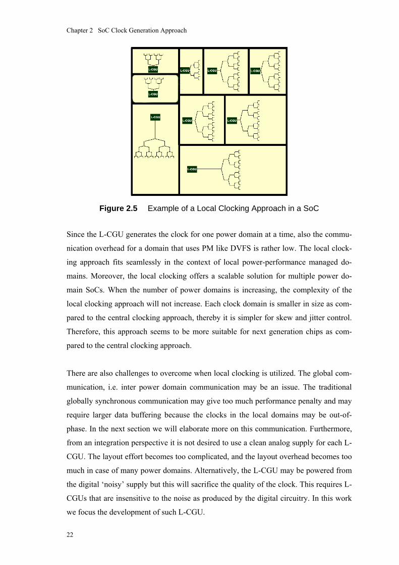
Figure 2.5 Example of a Local Clocking Approach in a SoC ................ 22
Figure 2.6 Example communication schemes for inter power domain
communications................................................................. 23
Figure 3.1 Time sequence iτ ............................................................. 27
Figure 3.2 Jitter metric definition [3.1]................................................... 29
Figure 3.3 Theoretical spectrum ( )ovS f of oscillator output ( )ov t [3.4] .. 30
Figure 3.4 Typical spectral components of oscillator phase noise [3.4] 33
Figure 3.5 Example colored noise spectra of PSN with same noise
variance............................................................................... 38
Figure 3.6 Numerical solution of expression (3.23)............................... 39
Figure 3.7 Inverter with positive input step signal [3.9] ......................... 40
Figure 3.8 Transfer curve for jitter from output noise [3.9] .................... 41
Figure 3.9 Equivalent circuit of an inverter for a rising output voltage... 43
Figure 3.10 Test-bench for the jitter of an inverter chain ........................ 46
Figure 3.11 Simulation results of the inverter chain................................ 47
Figure 3A.1 Noise folding effect of )( fS φ∆ [3.11]................................... 50
Figure 4.1 Integer-N PLL structure ....................................................... 53
Figure 4.2 Different oscillator types ...................................................... 54
Figure 4.3 Frequency divider phase model........................................... 63
Figure 4.4 Re-synchronization for a Frequency Divider........................ 64
Figure 4.5 The logic model and phase model of PFD-CP..................... 66
Figure 4.6 Spurs in output frequency spectrum [4.7] ............................ 67
Figure 4.7 Charge-pump output current in locked state due to noise

Master Thesis of Jinbo Wan
9
[4.8]………........................................................................... 67
Figure 4.8 Charge-pump output current in locked state due to mismatch
[4.8]….. ................................................................................ 68
Figure 4.9 Loop filter in a PFD-CP PLL ................................................ 69
Figure 4.10 Simulation result for the LF output at the condition of nonoise,
with Vdd noise and with gnd noise..................................... 70
Figure 5.1 General block diagram of the L-CGU................................... 73
Figure 5.2 Integer-N PLL structur ......................................................... 74
Figure 5.3 Structure of the differential ring-oscillator VCO.................... 76
Figure 5.4 Top level schematic of the differential ring VCO.................. 77
Figure 5.5 Replica bias for tuning the VCO .......................................... 77
Figure 5.6 Differential delay cell with symmetric load........................... 77
Figure 5.7 VCO output buffer................................................................ 78
Figure 5.8 Layout of the first differential ring-oscillator VCO................. 80
Figure 5.9 Simulation results of oscillation frequency versus tuning
voltage of the differential ring-oscillator VCO for various
process corners … ............................................................. 81
Figure 5.10 Phase noise of the differential ring-oscillator VCO at
1092MHz, no power supply noise. RMS period jitter (at
546MHz): 3ps……… ........................................................... 82
Figure 5.11 Phase noise of the differential ring-oscillator VCO at
1092MHz, with power supply noise added. RMS period jitter
(at 546MHz): 108ps ............................................................. 82
Figure 5.12 Power supply noise coupling to the output through load
resistors… ........................................................................... 83
Figure 5.13 Parasitics seen at the differential output of the delay cell .... 84
Figure 5.14 Reference ports of the tuning components influenced by
power supply noise.............................................................. 85
Figure 5.15 Sketched circuit for the improved differential ring VCO delay
cell……... ............................................................................. 86
Figure 5.16 Top level schematics for improved differential ring VCO ..... 86
Figure 5.17 Schematic circuit for the delay cell of the improved VCO .... 87
Figure 5.18 Layout of the improved differential ring-oscillator VCO........ 88
Figure 5.19 Simulated frequency tuning range at nominal process
List of Figures
10
corner…… ......................................................................... 89
Figure 5.20 Simulated phase noise at 1.092GHz under no power supply
noise, only power noise and only ground noise situations . 89
Figure 5.21 LC VCO part structure ......................................................... 90
Figure 5.22 Top level schematic of the LC VCO..................................... 91
Figure 5.23 Circuit schematic of the LC VCO ......................................... 92
Figure 5.24 Circuit schematic of the VCO output buffer.......................... 92
Figure 5.25 Layout of the LC VCO ......................................................... 94
Figure 5.26 Frequency range at all calibration situations........................ 95
Figure 5.27 LC VCO phase noise at 4.368GHz, no power supply noise 95
Figure 5.28 LC VCO phase noise at 4.368GHz, with power supply
noise……............................................................................. 96
Figure 5.29 Circuit schematic of the frequency divider FDIV M .............. 97
Figure 5.30 Circuit schematic of the frequency divider FDIV N .............. 98
Figure 5.31 Divide-by-2/3 cell logic......................................................... 98
Figure 5.32 Circuit schematic of the frequency divider FDIV X............. 100
Figure 5.33 The FDIV X buffer to convert a differential to single-ended
output…… ......................................................................... 100
Figure 5.34 Source Coupled Logic D-latch combined with an AND
function…. ......................................................................... 101
Figure 5.35 Layout of FDIV M............................................................... 102
Figure 5.36 Layout of FDIV N ............................................................... 102
Figure 5.37 Layout of the high-frequency divider FDIV X ..................... 103
Figure 5.38 PFD circuit schematic........................................................ 104
Figure 5.39 PFD layout......................................................................... 105
Figure 5.40 PFD circuit schematic........................................................ 106
Figure 5.41 Layout of the CP................................................................ 107
Figure 5.42 Loop filter circuit schematic ............................................... 108
Figure 5.43 Lock detector circuit schematic.......................................... 109
Figure 5.44 Lock detector circuit layout ................................................ 109
Figure 5.45 Top level schematic for the two differential ring PLLs........ 110
Figure 5.46 Top level schematic for the LC PLL................................... 110
Figure 5.47 Clock gating function, 50% duty cycle guarantee function and
clock re-synchronization function....................................... 111

Master Thesis of Jinbo Wan
11
Figure 5.48 The first differential ring PLL layout (60×60 2mµ )............... 113
Figure 5.49 The improved differential ring PLL layout (90×60µm2) ...113
Figure 5.50 The LC PLL layout (about 300×400 2mµ ) .......................... 114
Figure 5A.1 Symbol for the differential ring PLL.................................... 115
Figure 5A.2 Symbol for the improved differential ring PLL.................... 117
Figure 5A.3 Symbol for the LC PLL ...................................................... 119
Figure 5B.1 Logics to detect whether the VCO frequency need to be lower
or higher…......................................................................... 122
Figure 5B.2 Wave explanation for Figure 5B.1 ..................................... 123
Figure 6.1 Simulation test benches for the VCO frequency range test 126
Figure 6.2 Test benches for the whole PLLs transient simulation....... 130
Figure 6.3 Transient simulation of the first differential ring PLL in
transistor level…................................................................ 133
Figure 6.4 Transient simulation of the improved differential ring PLL in
transistor level at 546MHz output ...................................... 135
Figure 6.5 Transient simulation of the LC PLL in transistor level at
546MHz output…............................................................... 137
Figure 6.6 Phase noise ( )S fφ of the first differential ring PLL at 546MHz
output…… ......................................................................... 138
Figure 6.7 Phase noise ( )S fφ of the improved differential ring PLL at
546MHz output…............................................................. 139
Figure 6.8 Phase noise ( )S fφ of the LC PLL at 546MHz output ........ 139
Figure 6.9 Layout of the first implemented PLL test-chip in 65nm
CMOS……......................................................................... 143
Figure 6.10 Circuit schematic of the RF test buffer............................... 145
Figure 6.11 Layout of the RF test buffer ............................................... 145

List of Tables
12
List of Tables
Table 2.1 L-CGU Design Specifications .................................................... 25
Table 4.1 Oscillator types compare matrix ................................................ 63
Table 5.1 PLL output frequencies and divider numbers.......................... 74
Table 5.2 Frequency plan for LC VCO and the divider number of
FDIV_X…….. ................................................................................ 91
Table 5.3 Divide number settings for FDIV M ........................................... 97
Table 5.4 Divide number settings for FDIV N ........................................... 99
Table 5.5 Divide number settings for FDIV X (including ÷2 stage, which
is not shown in Figure 5.32 ) .................................................. 101
Table 5.6 Settings for CP and LF for the three implemented PLLs..... 108
Table 5A.1 Pins description for the differential ring PLL .......................... 115
Table 5A.2 Pins description for the improved differential ring PLL......... 117
Table 5A.3 Pins description for the LC PLL ............................................... 119
Table 6.1 Frequency range for each VCO under different process
corners…. .................................................................................... 127
Table 6.2 Jitter contributions of each PLL at 546MHz output............... 140
Table 6.3 PLL simulation results ............................................................... 141
Table 7.1 L-CGU Design Characteristics in 65nm LP-CMOS .............. 151

Master Thesis of Jinbo Wan
13
1. Introduction
CMOS technology scaling has been driven by Moore’s Law for more than forty years.
Nowadays, the minimum feature size in integrated circuit (IC) designs is as small as
45nm. ICs realised in such advanced CMOS technology can integrate a billion of tran-
sistors on the same silicon die. As CMOS technology advances, the integration density
is increased, which enables more cost-effective solutions and smaller form-factor de-
vices. Moreover, ICs fabricated in newer CMOS technologies can operate at higher
operating frequencies, thereby opening avenues for higher performance electronic prod-
ucts. Despite these benefits, the power consumption has become a major concern be-
cause the dense devices produce a significant amount of heat imposing constraints on
circuit performance and IC packaging. The case for portable devices is obvious, e.g. the
goal is to maximize battery time. Designing ICs for low power will be a key practical
and competitive advantage in the coming decade [1.1][1.2].
1.1. Clock Generation in Modern System Chips Modern system-on-chip (SoC) IC designs are getting equipped with multiple power
domains to meet the chip power-performance demands [1.3][1.4]. A power domain is a
region in the IC that is powered from its own dedicated power supply voltage (VDD), and
operates at its own dedicated frequency (f). A power domain may contain multiple
intellectual property (IP) cores of which each shared the same power-performance
demands. Figure 1.1 shows an example of a multiple power-domain SoC design in
which power domains are defined based on the functionality of the IP cores.
Figure 1.1 Example of a multiple power-domain SoC

Chapter 1 Introduction
14
In this respect, power domains are optimized to have power characteristics that are
unique from the rest of the design. On one hand, this may concern dedicated hardware
(HW) blocks that should operate at a fixed VDD and f. On the other hand, the may con-
cerns processor cores that require dynamic voltage and frequency scaling (DVFS).
Power domains may contain advanced power management features, e.g. clock gating,
power-down support with or without state-retention, DVFS, and defined operating
modes [1.5][1.6].
Traditionally, ICs make use of a custom-designed on-chip clock generator unit (CGU)
which produces the operating frequencies required in the whole chip design [1.7][1.8].
Typically, this component contains various phase-locked-loops (PLL) for frequency
generation, and they are referenced to a low-frequency crystal oscillator on the printed-
circuit-board (PCB). Also, it contains the frequency dividers and control logic for sup-
porting a wide range of operating frequencies and clock gating functionality. We will
refer to such CGU as central clock generator unit (C-CGU) in the remainder of this
report. With the increasing amount of power domains in the IC, also the need for more
independent operating frequencies increases. The CGU requirements for power domains
that need DVFS support will be more stringent, because the required frequency changes
at run-time. When only a few power domains are present in the IC, a C-CGU can meet
the requirements with moderate complexity. However, with the number of power do-
mains increasing, the operating frequencies required and the associated control over-
head will totally overwhelm the C-CGU, which constrains IC power-performance opti-
mization. Another issue with a C-CGU is the clock distribution which will become
problematic in large high-performance ICs [1.9]. This will degrade the quality of the
clock signals as provided to the local flip-flop registers in the design. Consequently,
larger design margins for clock uncertainty are needed that eventually degrade the
maximum performance of the IC.
An alternative, yet revolutionary clocking approach is the use of local clock generator
units (L-CGU) [1.10]. Each power domain contains its own L-CGU which generates the
required frequencies for the respective power domain. It can solve the problems associ-
ated to the C-CGU, and offers a modular and flexible clocking approach. However, the
challenge of an L-CGU is to generate a good quality clock while located in the close
proximity to the digital circuitry that acts as noise source. Furthermore, the penalty for a

Master Thesis of Jinbo Wan
15
clean analog VDD for each L-CGU becomes too high during chip integration. Finally,
the traditional globally synchronous inter power domain communication scheme needs
to be revisited.
1.2. Project Description This work concerns an investigation of clock generators suitable for use in a local
clocking scheme for digital logic CMOS circuits. Such L-CGU should have low-jitter
characteristics for providing a good quality clock to the power domain. It should be
programmable to support various operating frequencies with glitch-free frequency
transitioning to enable DVFS support. Also, it should support clock gating functionality
for standby operation. The L-CGU should operate from a ‘noisy’ digital power supply
voltage to simplify integration complexity. Finally, the L-CGU should have a minimum
overhead in terms of area occupation and power consumption. The following research
questions should be addressed:
• What kinds of oscillator are suitable for L-CGU application?
• How the power supply noise influence the jitter of the L-CGU?
• What is the lowest possible jitter that can be achieved by an L-CGU?
• What the clock buffer network influence to the final jitter performance when the
L-CGU output need to be distributed?
Potential candidate L-CGUs should be compared on their characteristics (e.g. jitter,
power consumption, area, etc.). The outcome of this work should be an implementation
of the most promising clock generator in 65nm LP-CMOS. Furthermore, the clock
buffer jitter contribution should also be investigated, which will serve as a starting point
for optimizing the clock distribution network.
1.3. Report Outline Chapter 2 will review the clock generation approach and compare C-CGU and L-CGU.
The requirements for the L-CGU design will be presented at the end of Chapter 2.
Chapter 3 will focus on jitter analysis. The relationship between jitter and phase noise
will be discussed. Power supply noise influence to jitter will be studied. And at last the
jitter produced by the clock buffer in the clock distribution networks will be discussed.
Chapter 4 will present the L-CGU system structure and the brief analysis for each part
in the L-CGU. Chapter 5 will show both schematics and layout of the L-CGU. The

Chapter 1 Introduction
16
simulation results and test bench will be introduced in Chapter 6. And finally, Chapter 7
concluded the thesis work and prospect the future works.
Reference [1.1] J. Kim et. al., “A Low Power SOC Architecture for The V2.0+EDR Blue-
tooth,” International Conference on Consumer Electronics, p1-15, Jan. 2008.
[1.2] A. C. W. Wong et. al., “A 1V Wireless Transceiver for an Ultra Low Power
SoC for Biotelemetry Applications,” 33rd European Solid State Circuits Con-
ference, Sept. 2007,
[1.3] K. Flautner et. al., “IEM926: an Energy Efficient SoC with Dynamic Voltage
Scaling,” Proceedings of the Design, Automation and Test in Europe Confer-
ence and Exhibition, vol. 3, 324-327, Feb. 2004.
[1.4] T. Hattori et. al., “Hierarchical Power Distribution and Power Management
Scheme for a Single Chip Mobile Processor,” 43rd ACM/IEEE Design Auto-
mation Conference, 292-295, San Francisco, Jul. 2006.
[1.5] K. Funaoka et. al., “Dynamic Voltage and Frequency Scaling for Optimal Real-
Time Scheduling on Multiprocessors,” International Symposium on Industrial
Embedded Systems, 27-33, La Grande Motte, Jun. 2008.
[1.6] E. Beigne et. al., “Dynamic Voltage and Frequency Scaling Architecture for
Units Integration within a GALS NoC,” International Symposium on Net-
works-on-Chip, 129-138, Apr. 2008.
[1.7] L. Joonhee et. al., “A 480-MHz to 1-GHz Sub-Picosecond Clock Generator
With a Fast and Accurate Automatic Frequency Calibration in 0.13-µm
CMOS,” IEEE Asian Solid-State Circuits Conference, 67-70, Nov. 2007.
[1.8] J. Goto et. al., “A Programmable Clock Generator With 50 to 350 MHz Lock
Range for Video Signal Processors,” Proceedings of the IEEE Custom Inte-
grated Circuits Conference, 4.4.1-4.4.4, May 1993.
[1.9] A. V. Mule et. al., “Electrical and Optical Clock Distribution Networks for
Gigascale Microprocessors,” IEEE Transactions on Very Large Scale Integra-
tion (VLSI) Systems, vol. 10, is. 5, 582-594, Oct. 2002.
[1.10] T. Olsson, P. Nilsson, “A Low-Complexity Method for Distributed Clocking
on Digital ASICs,” Proceedings of 2004 IEEE Asia-Pacific Conference on Ad-
vanced System Integrated Circuits, 344-347, Aug. 2004.

Master Thesis of Jinbo Wan
17
2. SoC Clock Generation Approach
Power efficient design technologies have become key drivers in modern integrated
circuits targeting portable to high-performance application ranges. The implementation
of circuits and systems in new deep submicron technologies requires new ideas to make
the system performance successfully feasible. In this chapter we will first elaborate on
the clocking needs in high-performance digital logic CMOS circuits. Next, we will
review the central and local clocking approaches for power domain SoCs, and discuss
inter domain communication schemes. Finally, we formulate the requirements for the L-
CGU design.
2.1. Clocking Requirements for Digital Logic Blocks The ongoing CMOS technology scaling enables higher frequency operation. The shorter
clock periods require also a reduction of timing margins for maximizing the useful cycle
time. Consequently, clock design becomes increasingly challenging for meeting clock,
skew and jitter targets.
Traditionally, circuit designers use 10% clock uncertainty margin of the total clock
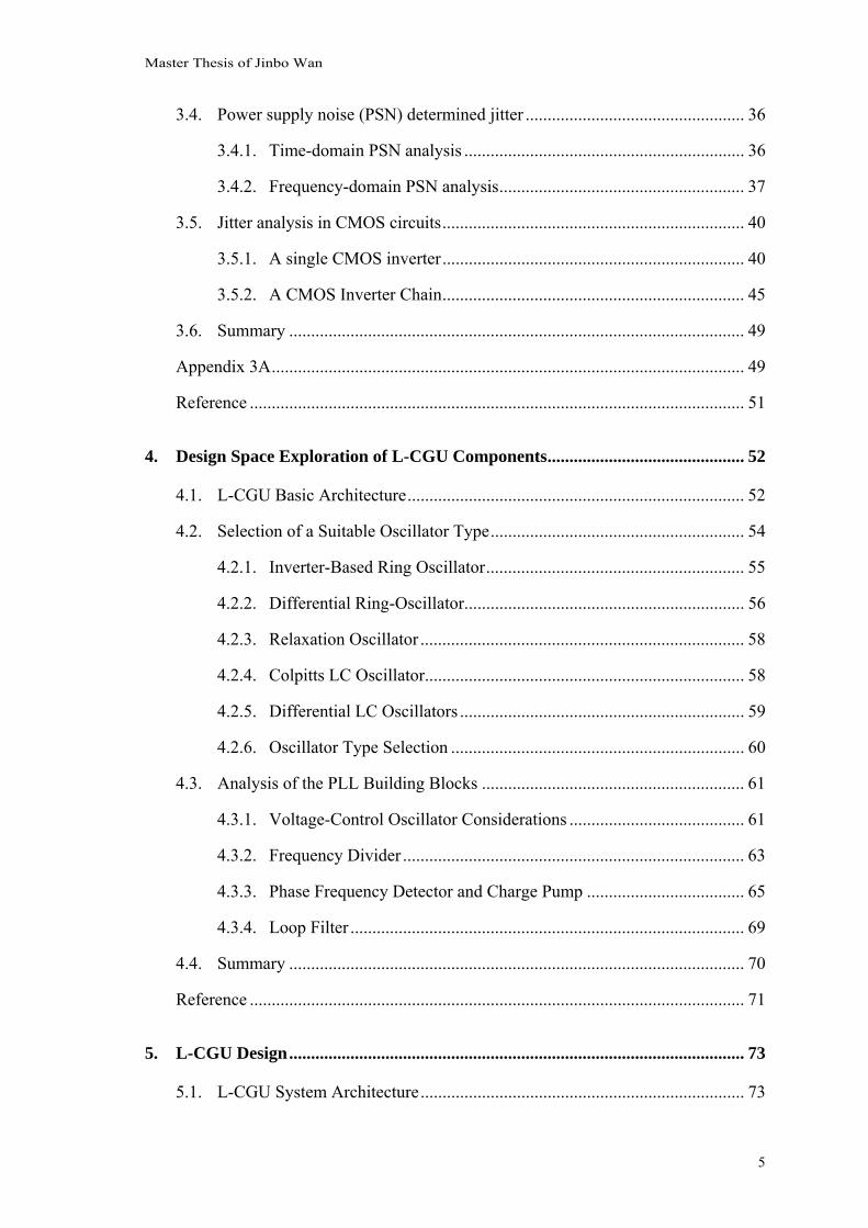
budget when implementing their circuits. Figure 2.1 puts in perspective the influence of
clock uncertainty on circuit area and performance. The values have been obtained from
logic synthesis for maximum speed with Cadence Ambit for a RISC processor design in
65nm LP-CMOS. In this example, the use of a clock uncertainty of 300ps results in an
area penalty of 20% with respect to the case of no clock uncertainty. Alternatively, the
minimum clock period can be decreased by 8%, leading to an improved circuit per-
formance. Although the use of a ‘no clock uncertainty’ margin is not realistic, the de-
sign over-dimensioning for larger clock uncertainties has become evident. A high-
quality clock generation and clock distribution is of prime importance in high-
performance IC designs.
Chapter 2 SoC Clock Generation Approach
18
0
5000
10000
15000
20000
25000
30000
3.2 3.4 3.6 3.8 4.0 4.2 4.4 4.6 4.8 5.0 5.2 5.4
Clock Period [ns]
Cir
cuit
Are
a [u
m2]
clock uncertainty: [0,100,200,300]ps
-20%
-8%
Figure 2.1 Circuit area versus performance for different clock uncertainty settings for a RISC processor design in 65nm LP-CMOS
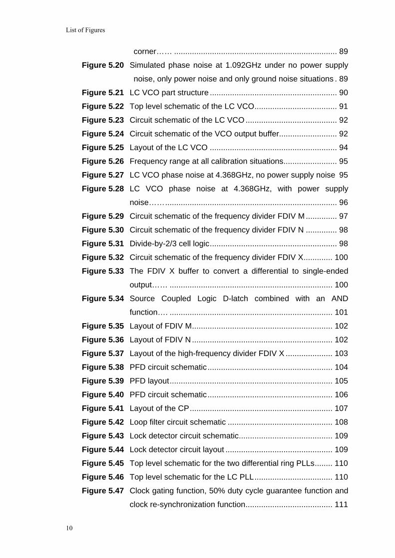
The power consumption in modern ICs has become of a primary concern. The use of
power domain approaches is a means to further reduce power consumption by selecting
optimum VDD’s and frequencies at design-time or during circuit operation. An example
of a power management (PM) technique for reducing active-mode power consumption
is dynamic voltage and frequency scaling (DVFS) [2.1]. DVFS can be utilized only in
those cases where the circuit does not require peak performance. Significant power
savings can be achieved. Figure 2.2 illustrates the dependency between frequency and
power consumption when operating at the optimum VDD (ref. DVFS).
0.0
0.2
0.4
0.6
0.8
1.0
0.0 0.1 0.2 0.3 0.4 0.5 0.6 0.7 0.8 0.9 1.0
Relative Power Consumption
Rel
ativ
e O
pera
ting
Freq
uenc
y
1.2V
1.1V
1.0V
0.9V
0.8V
0.7V
0.6V
Figure 2.2 Frequency versus Power Consumption for Different Supply Voltage Settings for a 65nm LP-CMOS ring-oscillator circuit
Master Thesis of Jinbo Wan
19
DVFS requires a clock generator that supports multiple clock frequencies. Without
frequency scaling support, this PM technique can not be utilized. Moreover, the transi-
tioning between frequency points needs to be free of spurious glitches since the circuit
is operational at that time. It also needs to be fast, because this offers the most power
benefits. Furthermore, a sequence is need between frequency and VDD control in order
to guarantee circuit operation. For example, the frequency needs to be reduced before
the VDD is reduced, and the VDD must be increased before the frequency is increased.
The required frequency control needs intelligence clock management. Especially, in
multiple power-domain ICs the clock management can become a bottleneck, depending
on the amount of power domains that require DVFS support.
Finally, modern ICs also require standby-mode power management. Clock generators
need to be equipped with clock gating support to avoid the needless switching of circuit
nodes while the clock generator is still running. There should also be clock enable
support to fully stop the clock generator, which reduces its power consumption to a
minimum.
2.2. Review of the Central Clocking Approach The traditional clock generation scheme in digital SoCs is the centralized or global
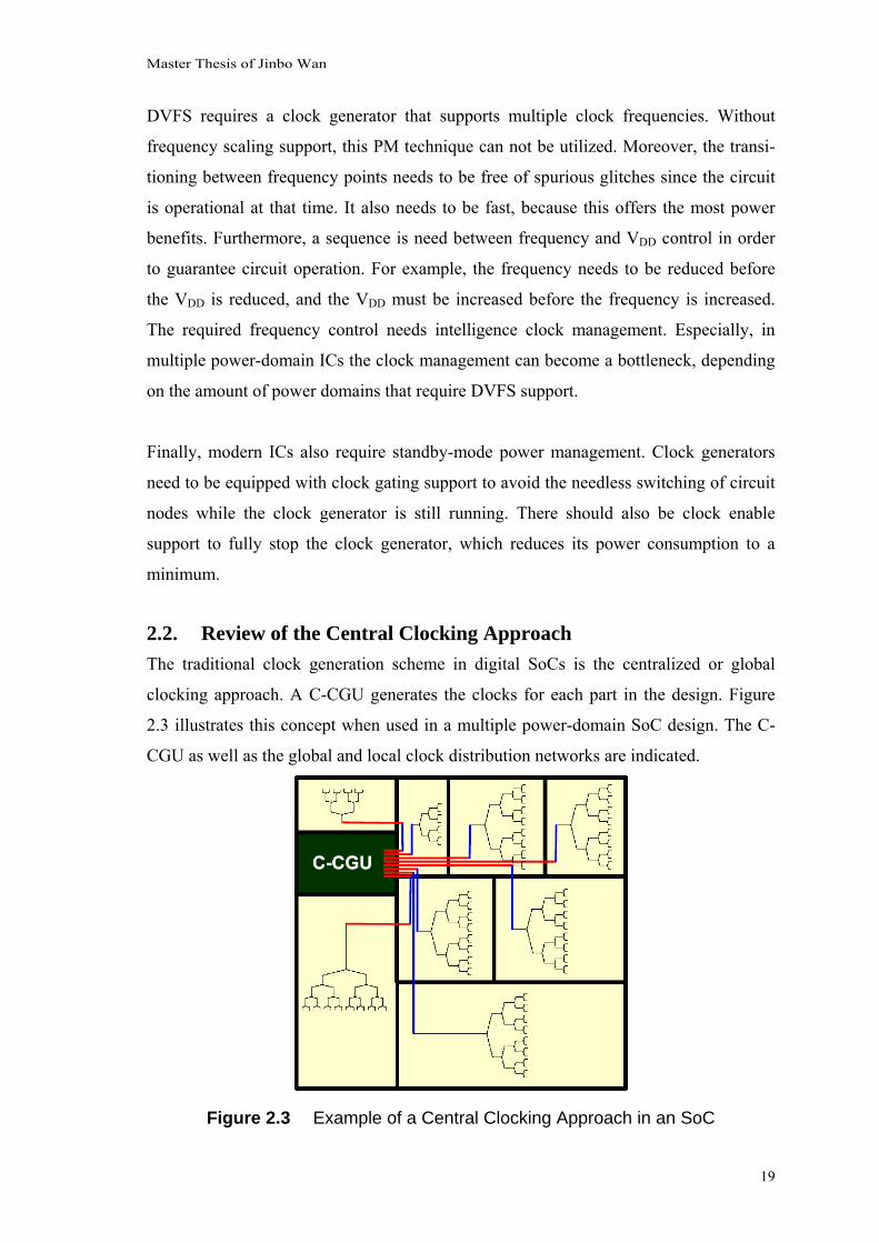
clocking approach. A C-CGU generates the clocks for each part in the design. Figure
2.3 illustrates this concept when used in a multiple power-domain SoC design. The C-
CGU as well as the global and local clock distribution networks are indicated.
Figure 2.3 Example of a Central Clocking Approach in an SoC

Chapter 2 SoC Clock Generation Approach
20
The main benefit of a central clock is that the C-CGU can be supplied from its own
clean analog power supply and ground connections. Although this requires extra pack-
age pins, it is very effective to suppress the influences of noise as generated by the
digital circuitry. Consequently, this will improve the quality of the clock.
The drawbacks of a C-CGU are as follows. Since there is only one clock generator in
the SoC, it needs to support all the required operating frequencies for the HW blocks.
This makes the C-CGU complicated. Moreover, the clock management may be dramati-
cally complex for a larger number of power domains. Each power domain needs to
interact with the C-CGU to request a certain frequency of operation, or clock gating for
standby mode. This will result in a communication bottleneck in case many power
domains communicate with the C-CGU. Furthermore, for each SoC their may be differ-
ent clocking needs and C-CGU customization is required, or alternatively, a generic C-
CGU is taken which is not used to its full potential.
An example of a C-CGU is shown in Figure 2.4. Modern C-CGUs can easily contain
tens of phase-locked-loops (PLL) and several reference inputs. The C-CGU shown in
Figure 2.4 is a programmable CGU. The number of external clock inputs, PLLs (and
type), frequency dividers (and type), and clock outputs are selectable at compile time.
Test control block (TCB) determines the C-CGU working mode. Design for debug
(DfD) and delay fault test (DFT) blocks are used to monitor the PLLs status and test.
Power (PWR) block control the CGU power consumption by setting some PLLs into
sleep mode when they are not needed.
Figure 2.4 A central CGU example

Master Thesis of Jinbo Wan
21
The clock distribution for a central clocking scheme is becoming extremely challenging
for high-performance ICs. On one hand this is caused by the further CMOS technology
scaling. The die area may not scale with the same amount as the transistor area, thus, the
coverage area for clock distribution may increase. On the other hand, higher perform-
ance operation reduces the cycle time. The clock uncertainty margin needs to be scaled
accordingly to have the maximum benefit from performance increase due to technology
scaling. In a central clocking scheme, the clock needs to distribute globally (to the
different HW blocks) and locally (within each HW block). It is essential that all regis-
ters, or leaf cells of the clock distribution, receive the clock in-phase (or at a defined
phase-shift) with the master clock to avoid communication problems. These matters
make a central clocking scheme not easily scalable. The clock distribution itself is also a
source of clock uncertainty. Since the clock buffers are typically powered from the
digital ‘noisy’ supply to lower implementation complexity, they are sensitive to the
power supply noise that exists on the supply due to the switching digital circuitry. As a
result, the quality of the clock signal at the output of the clock generator is degraded to a
large extent when it arrives at the receiving flip-flop clock input. For clock skew man-
agement, a place-and-route tool inserts many clock buffers in clock distribution network,
however, the clock jitter increases for the amount of clock buffers in the path are in-
creasing. Thus, the clock quality is very much dependent on the clock tree optimization.
2.3. Review of the Local Clocking Approach A local clocking approach can alleviate the drawbacks associated to a central clocking
approach. Now, each power domain is equipped with its own L-CGU, and it needs to
provide the clock frequencies to all HW blocks that share the same power domain.
Typically, a power domain contains a single HW block, and the L-CGU only needs to
provide a single clock. Figure 2.5 illustrates the local clocking concept when used in a
multiple power-domain SoC design. Observe from this Figure, the modularity of a local
clocking approach. The global clock distribution network as found in the central clock-
ing approach is not required in case of local clocking.
Chapter 2 SoC Clock Generation Approach
22
Figure 2.5 Example of a Local Clocking Approach in a SoC
Since the L-CGU generates the clock for one power domain at a time, also the commu-
nication overhead for a domain that uses PM like DVFS is rather low. The local clock-
ing approach fits seamlessly in the context of local power-performance managed do-
mains. Moreover, the local clocking offers a scalable solution for multiple power do-
main SoCs. When the number of power domains is increasing, the complexity of the
local clocking approach will not increase. Each clock domain is smaller in size as com-
pared to the central clocking approach, thereby it is simpler for skew and jitter control.
Therefore, this approach seems to be more suitable for next generation chips as com-
pared to the central clocking approach.
There are also challenges to overcome when local clocking is utilized. The global com-
munication, i.e. inter power domain communication may be an issue. The traditional
globally synchronous communication may give too much performance penalty and may
require larger data buffering because the clocks in the local domains may be out-of-
phase. In the next section we will elaborate more on this communication. Furthermore,
from an integration perspective it is not desired to use a clean analog supply for each L-
CGU. The layout effort becomes too complicated, and the layout overhead becomes too
much in case of many power domains. Alternatively, the L-CGU may be powered from
the digital ‘noisy’ supply but this will sacrifice the quality of the clock. This requires L-
CGUs that are insensitive to the noise as produced by the digital circuitry. In this work
we focus the development of such L-CGU.
Master Thesis of Jinbo Wan
23
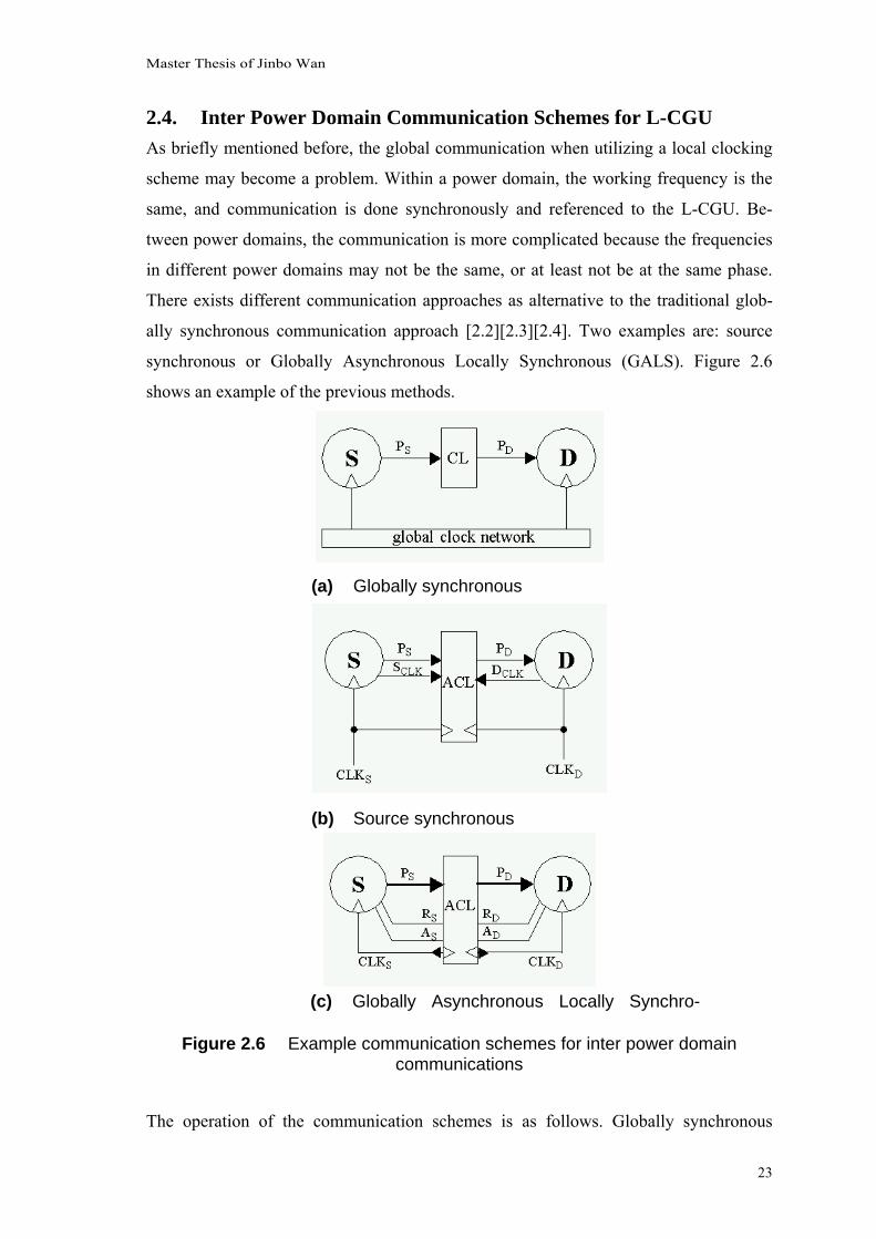
2.4. Inter Power Domain Communication Schemes for L-CGU As briefly mentioned before, the global communication when utilizing a local clocking
scheme may become a problem. Within a power domain, the working frequency is the
same, and communication is done synchronously and referenced to the L-CGU. Be-
tween power domains, the communication is more complicated because the frequencies
in different power domains may not be the same, or at least not be at the same phase.
There exists different communication approaches as alternative to the traditional glob-
ally synchronous communication approach [2.2][2.3][2.4]. Two examples are: source
synchronous or Globally Asynchronous Locally Synchronous (GALS). Figure 2.6
shows an example of the previous methods.
Figure 2.6 Example communication schemes for inter power domain communications
The operation of the communication schemes is as follows. Globally synchronous
(a) Globally synchronous
(b) Source synchronous
(c) Globally Asynchronous Locally Synchro-

Chapter 2 SoC Clock Generation Approach
24
communication (see Figure 2.6a) uses a global clock reference to communicate between
a sending power domain and receiving power domain over a Connection Link (CL). It
requires a clock in the chip that is properly balanced. This communication scheme is
simple but faces insertion delay, high power and clock skew problem. Source Synchro-
nous is more complicated (see Figure 2.6b), there is a buffer needed in which data is
stored by using a source clock, and data is read by using a destination clock. The buffer
is indicated in Figure 2.6b as Asynchronous Connection Link (ACL). The clock-data
skew is critical in this approach. Source Synchronous communication is suitable for use
in combination with a local clocking approach since both source and destination clocks
are used for the communication. The imbalance of these clocks has an effect on the
buffer size. GALS communication is realized by handshake (or asynchronous) control.
As in case of Source Synchronous, there is a buffer in which data is stored and data is
read from. Synchronous communication is used within the power domains. Also, GALS
communication is suitable for use in combination with a local clocking approach.
At this point it should be clear that there exist global communication schemes suitable
for inter power domain communications when power domains are equipped with an L-
CGU. The global communication is beyond the scope of this work. Our focus is on is on
the clock generation and clock distribution, particularly the design of an L-CGU.
2.5. L-CGU Requirements and Design Specifications In this section we will summarize the requirements and design specifications related to
the L-CGU design.
The main requirement is an L-CGU topology that is insensitive to external noises (i.e.
power supply noise, substrate noise, …) such that the L-CGU is able to generate a high
quality clock. The L-CGU output frequency should be accurate and stable, i.e. the clock
jitter should be as low as possible. The output frequency should be independent of
process parameter variations and temperature conditions. The L-CGU should be pow-
ered from the digital ‘noisy’ supply to simplify the IC top-level integration.
Other requirements are: 1) the L-CGU should be fully integratable in bulk CMOS tech-
nology, 2) a small circuit area, 3) a low active and static power consumption, 4) the L-
CGU should support multiple frequency points, frequency scaling, clock gating for L-

Master Thesis of Jinbo Wan
25
CGU output gating and clock enabling for full L-CGU stop, 5) seamless and glith-free
frequency transitioning, 6) a digital L-CGU interface for frequency programming, and 7)
an output signal that indicates if the L-CGU output is stable.
The L-CGU design should be implemented in a 65nm LP-CMOS technology. The
previous summarized requirements have been translated into design specifications of
the L-CGU, which are shown in Table 2.1. These design specifications have been used
as the basis for the L-CGU design which will be shown in the following chapters.
Table 2.1 L-CGU Design Specifications
Items Requirements
CMOS technology 65nm LP-CMOS
Supported Operating
Frequencies
550MHz, 500MHz, 450MHz, 400MHz, 350MHz, 300MHz,
250MHz, 200MHz, 150MHz, 100MHz, 50MHz
Jitter specification Max RMS period jitter<30ps at 550MHz output frequency
Frequency Switching • Switch time as small as possible
• Glitch-free frequency transitioning
• Clock gating and clock enabling support
Area Occupation At least <0.1mm2, as small as possible
Active Power Con-
sumption
Lower than 1mW
L-CGU Supply Volt-
age • Nominal digital VDD of 1.2V
L-CGU Outputs Clock frequency signal, clock valid signal
2.6. Summary In this chapter, the clock requirements for the digital logic blocks in modern SoC design
are first reviewed. The two approach for clock generation: the L-CGU and the C-CGU
are investigated. Depends on these reviews, the requirements for the L-CGU are pre-
sented. Also the inter power domain communication schemes for the L-CGU is briefly
examined. Next chapter, we will analyze the requirements for the L-CGU. The most
critical one—jitter performance, will be focused.

Chapter 2 SoC Clock Generation Approach
26
Reference [2.1] G. Semeraro, D. H. Albonesi, S. G. Dropsho, G. Magklis, S. Dwarkadas, and M.
L. Scott, “Dynamic frequency and voltage control for a multiple clock domain
microarchitecture,” in Proc. IEEE/ACM Int. Symp. Microarch., 2002, pp. 356–
367.
[2.2] E. Reese et al., “A Phase-Tolerant 3.8 GB/s Data-Conimunicatioii Router for a
Supercomputer Backplane“, ISSCC Digest of Technical Papers, pp. 296-297,
February 1994.
[2.3] D. M. Chapiro, “Globally-asynchronous locally-synchronous systems,” Ph.D.
dissertation, Comput. Sci. Dept., Stanford Univ., Palo Alto, CA, 1984.
[2.4] D. Bormann and P. Cheung, “Asynchronous wrapper for heterogeneous sys-
tems,” in Proc. ICCD, 1997, pp. 307–314.
Master Thesis of Jinbo Wan
27
3. Jitter Performance Models
The most critical requirement of the L-CGU is the quality of the output clock signal,
which is quantified by the timing jitter. Although jitter is widely used, the symbols and
definitions of jitter are still not unique. In this chapter, we will first provide the reader
with an overview and definition of jitter as used in this work, and its relation to phase
noise. Next, we present the jitter due to power supply noise, and the associated power
supply noise model used for emulating a noisy digital environment. Finally, we analyze
the jitter performance of a single CMOS inverter as well as a CMOS inverter chain.
3.1. Jitter Definitions Jitter is measure for the clock uncertainty in time domain. In this section we will use the
jitter definitions from Ken Kundert [3.1].
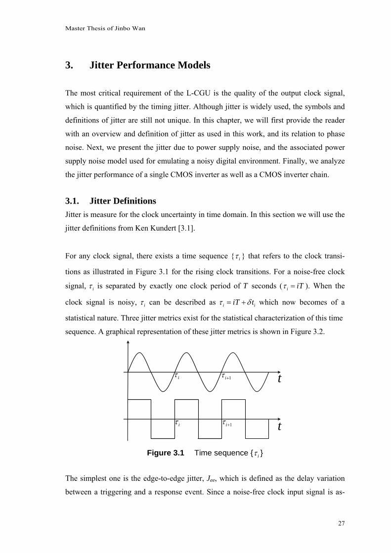
For any clock signal, there exists a time sequence iτ that refers to the clock transi-
tions as illustrated in Figure 3.1 for the rising clock transitions. For a noise-free clock
signal, iτ is separated by exactly one clock period of T seconds ( i iTτ = ). When the
clock signal is noisy, iτ can be described as i iiT tτ δ= + which now becomes of a
statistical nature. Three jitter metrics exist for the statistical characterization of this time
sequence. A graphical representation of these jitter metrics is shown in Figure 3.2.
Figure 3.1 Time sequence iτ
The simplest one is the edge-to-edge jitter, Jee, which is defined as the delay variation
between a triggering and a response event. Since a noise-free clock input signal is as-
t
t
iτ
iτ
1iτ +
1iτ +

Chapter 3 Jitter Performance Models
28
sumed, the edge-to-edge RMS jitter eeJ can be described as
2 ( ) var( ) var( ) var( )ee i i iJ i iT tτ δ τ= − = = (3.1)
Jee is an input referred jitter metric which is only defined for driven systems. Examples
of driven systems are: a phase-frequency detector (PFD), a frequency divider (FDIV)
and clock buffer. For such systems, a transition at the output is a direct result of a transi-
tion at the input. The reason why Jee is only defined for driven systems is because the
reference point is fixed and free of noise. Consequently, it can not be used for autono-
mous systems such as a voltage-controlled oscillator (VCO).
The second jitter metric is K-Cycle jitter, kJ . Jk measures the uncertainty of the clock
signal over k clock cycles. It is defined as the standard deviation of i k iτ τ+ − .
2 ( ) var( )k i k iJ i τ τ+= − (3.2)
The reference point (τi) refers to a point on a previous k -cycle transition, and therefore
it is not free of noise which increases the jitter. K-Cycle jitter is suitable as a metric in
both driven and autonomous systems. A special case is found for k=1; J1 is the standard
deviation of the length of a single clock period. This case is often referred as period
jitter or cycle jitter, which is denoted as J (where J=J1). In Cadence SpectreRFTM, K-
Cycle jitter is expressed as cJ .
The third jitter metric is cycle-to-cycle jitter, Jcc. Consider 1i i iT τ τ+= − to be the period
of cycle i . Now, Jcc can be described as 2
1( ) var( )cc i iJ i T T+= − (3.3)
Jcc is a jitter metric for identifying large adjacent clock cycle displacements. It is similar
to edge-to-edge jitter because it does not contain information about the correlation in the
jitter between distant clock transitions. However, the difference is due to the fact that it
is a measure of short-term jitter, because it is relatively insensitive to long-term jitter.
That is to say it can get rid of flicker noise influence. Also, Jcc is suitable as a metric in
both driven and autonomous systems.

Master Thesis of Jinbo Wan
29
Figure 3.2 Jitter metric definition [3.1]
If the clock signal noise is either stationary or T-cyclostationary [3.1], then the time
sequence iτ is stationary. This means that the jitter metrics do not vary with i . Con-
sequently, ( )eeJ i , ( )kJ i , and ( )ccJ i can be written as eeJ , kJ , and cJ .
We will use period jitter, J, for characterizing the performance of the L-CGU compo-
nents. The values of J, which will be shown in the remained chapters, are the root-
mean-square (rms) value, not the peak value.
3.2. Phase noise Jitter is a simple measure of the clock quality. Yet it cannot give much insight into the
design. Based on the jitter measurement, we don’t know important information such as
which parts of the circuit dominate the jitter performance and need to be improved, or
which circuit part doesn’t matter and can be relaxed in its design requirements. Corre-
spondingly, phase noise can give much insight to help the design and is more familiar to
oscillator designers. What’s more, the relationship between jitter and phase noise is
determined and very clear.
There exists several different spectral density functions commonly used to characterize
phase noise [3.2][3.3]. In this section we referred to the definition in Gardner’s book
[3.4] and only elaborate on those functions that are relevant for this work. For this
purpose, we make use of a generic oscillator whose output voltage ( )ov t has a sinusoi-
dal waveform at a nominal frequency 0f Hertz.
0( ) cos[2 ( )]ov t A f t tπ φ= + (3.4)

Chapter 3 Jitter Performance Models
30
where A is the voltage amplitude, and ( )tφ contains all phase and frequency deviations
from the nominal frequency 0f and phase 02 f tπ . The presence of amplitude noise is not
separately accounted for because oscillators contain an amplitude-control mechanism
largely suppress this noise. Hence, we treat all the noise as phase noise.
3.2.1. ( )ovS f : Passband spectrum of the oscillator signal ( )ov t
( )ovS f is the Fourier transform of the autocorrelation function of the random process
( )ov t . It is one-side spectral description, and requires a stationary autocorrelation func-
tion. Figure 3.3 shows an example of ( )ovS f for three different cases of phase noise.
When phase noise is absent, the spectrum contains a single frequency at 0f and can be
expressed as2
0( )2A f fδ − . When phase noise occurs, the spectrum is spread. Irrespec-
tive of the amount of phase noise present in the signal, the integral of ( )ovS f over all
frequencies equals 2
2A . In other words, the variance of ( )ov t equals
2
2A .
2
0
var[ ( )] ( )2oo vAv t S f df
∞
= =∫ (3.5)
Figure 3.3 Theoretical spectrum ( )ovS f of oscillator output ( )ov t [3.4]
3.2.2. ( )L f∆ : Single Side Band (SSB) Phase Noise
SSB phase noise ( )L f∆ is the normalized version of ( )ovS f , which is defined as
2
)()( 2
0
AffS
fL ov ∆+=∆ (3.6)
( )L f∆ is the noise power, relative to the total power in the signal, in a bandwidth of
( )ovS f

Master Thesis of Jinbo Wan
31
1Hz in a single sideband at a frequency offset f∆ from the carrier frequency 0f . The
value of ( )L f∆ is commonly expressed as )](log[10 fL ∆ dBc/Hz. dBc means “dB
relative to carrier,” where the term “carrier” actually means total power in the signal. In
fact, in SpectreRFTM, ( )L f∆ is calculated by the noise power divide fundamental fre-
quency power, not the total power. This is a good approximation for a sinewave oscilla-
tor output, but is not correct for other waveforms such as square wave.
3.2.3. ( )S fφ : Baseband spectrum of the phase noise ( )tφ
Both ( )ovS f and ( )L f∆ are spectra of the physical RF signal ( )ov t . Their peaks are at
the carrier frequency 0f , and their sidebands are located at either side of the peaks.
Contrarily, ( )S fφ is defined as a low-pass, single-side spectrum of phase noise modula-
tion ( )tφ . This baseband phase noise expression is more convenient for use in our calcu-
lations. J.A.Barnes et.al. [3.5] showed that the continuous phase noise spectra can be
well approximated as
01
22
33
44)( c
fc
fc
fc
fc
fS ++++=φ , (3.7)
where ic is a constant.
The 44
fc term is the result of random walking noises which modulate the frequency. It is
only relevant to consider for high-precision frequency standards, i.e., atomic frequency
standards, at frequency well below 1Hz. This term can be neglected in case of PLLs.
The 33
fc term is due to flicker noises which modulate the frequency, also called flicker
FM phase noise. For a high frequency reference PLLs, this component comes from the
VCO, and can be greatly suppressed by the loop. Moreover, when calculating the period
jitter from phase noise, the contribution of this phase noise component is very small
[3.6]. Therefore, we do not account for this noise, unless the corner between 33
fc term
and 22
fc term, flicker corner, is beyond the PLL loop bandwidth.

Chapter 3 Jitter Performance Models
32
The 22
fc term comes from white noise that modulates the frequency, also called white
FM phase noise. This phase noise is the most relevant one in oscillators and PLLs. Most
of the phase noise as referred to in this work, relates to this phase noise component.
The fc1 term is caused by flicker noise phase modulation, often called flicker PM phase
noise. Typically, it is only present in a narrow frequency range, and sometimes even
overlapping with white FM phase noise. Therefore, we do not consider this phase noise
component in this work.
Finally, 0c is the noise floor due to white noise phase modulation. For PLLs, this noise
comes from driven components which do not influence the oscillation frequency, e.g.,
the frequency divider and other digital logic and buffer circuits. These circuits add
uncorrelated phase noise to the noise floor. In fact, most of the jitter contributed by
clock buffers is from this part. It is considered an important component in this work.
Figure 3.4 shows a graphical representation of expression (3.7). In a log-log plot, this
expression provides a piece-wise linear representation of the phase noise spectrum and
frequency dependency. Each line segment has different slopes as illustrated in Figure
3.4.

Master Thesis of Jinbo Wan
33
Figure 3.4 Typical spectral components of oscillator phase noise [3.4]
In summary, we will consider only the 22
fc
and 0c phase noise parts which are the
result of white noise sources. Consequently, we simplify expression (3.6) to
022)( c
fcfS +=φ (3.8)
3.3. Phase noise and jitter relationship Phase noise is a continuous stochastic process indicating random accelerations and
decelerations in phase φ as an oscillator orbits at a nominally constant frequency 0f in
steady state [3.6]. Jitter arises from sampling the orbit at certain points (transition
points). The two are fundamentally different and the relationship is not obvious. In this
section we will derive simplified relationships between jitter and phase noise.
A noisy clock output signal )(tvn can be expressed as a noise-free signal )(tv , plus a
noise )(tn . An alternative representation is to add a jitter term )(tj to time t . Yet an-
-40dB/decade (c4/f4)
-30dB/decade (c3/f3)
-20dB/decade (c2/f2)
-10dB/decade (c1/f)
0dB/decade (c0)
log(f)
10 lo
g[3.
Sф
(f)] (
dB )

Chapter 3 Jitter Performance Models
34
other representation is use phase noise ( )tφ instead of the jitter term, since )(tj can be
translated to phase by multiply 02 fπ . This gives
]2
)([
)]([)()()(
0fttv
tjtvtntvtvn
πφ
+=
+=+=
(3.9)
For time points when )(tvn is positive-going and crossing the threshold value, normally
zero for sinewave and 2ddV for a digital clock, we obtain a sequence of time points
iτ
2
)()(
0ft
ttjt iiiii π
φτ +=+= . (3.10)
While combining (3.2) and (3.10), we obtain the following expression for period jitter
20
20
2
4)](var[
]2
)(var[
ft
ft
J ii
πφ
πφ ∆
=∆
= (3.11)
where f0 is the oscillation frequency, and )()()( 1 iii ttt φφφ −=∆ + .
The variance of )( itφ∆ can be calculated by using the Wiener-Khinchine theorem [3.7].
The deducing procedure is shown in Appendix 3A. Finally we get the exact relationship
between jitter and phase noise, shown in expression (3.12).
∫ ∆=∆
=2
0_2
022
02
20
)(4
14
)](var[ f
foldi dffS
fft
J φππφ
(3.12)
In the expression (3.12), )(_ fS foldφ∆ is the folded version of )( fS φ∆ by sample effect
and defined only over the frequency range [0, 20f ].
In practice, the phase noise of an oscillator is very small for frequencies beyond 20f .
As a result, the spectrum folding of )( fS φ∆ due to sampling can be neglected. There-
fore, the relationship between period jitter and phase noise can be approximated with a
simpler expression. By combining (3.12) and other expressions in Appendix 3A, we

Master Thesis of Jinbo Wan
35
obtain the commonly used general form of the jitter and phase noise relationship.
dff
fffSdffS
fJ ∫∫
∞∞
∆ =≈0
20
02
02
02
2
)()(sin
)()(4
1ππ
π φφ (3.13)
To further simplify (3.13), we will now determine jitter and phase noise relationship for
the special case when phase noise arises from white noise sources only. Next, we will
consider phase noise ( )S fφ that consists of two components, namely 22
fc and 0c as
shown in (3.8).
3.3.1. White PM phase noise only (noise floor): ( )S fφ = 0c
For this phase noise component, the integration result of (3.13) is infinite when the
upper integration limit is infinite, which means that the jitter is infinitely large. The
error comes from the upper limit of the integration. In fact, the noise floor is influenced
by the spectrum folding. The spectrum folding due to sampling effect makes the inte-
gration upper limit finite, as in case of (3.12). Lee et.al. showed that the upper integra-
tion limit can be approximated by 20f in case of white PM phase noise [3.8]. As a
result, (3.13) can be re-written to
2 02 2
0 0
1( )(2 ) 4
cJ S ff fφπ π
= = ⋅ (3.14)
3.3.2. White FM phase noise only (-20dB/dec): ( )S fφ = 22
fc
The integration of (3.13) is finite in case of white FM phase noise. Lee et.al. showed
the use of an upper integration limit of ∞ for this noise component. Therefore, we
obtain
30
2
30
23
0
2
02
2
30
2
02
0
02
222
2)(
22sin
)()(sin
fffS
fc
fc
dxx
xfc
dff
fffc
J ⋅==⋅=== ∫∫∞∞
φπ
ππππ
(3.15)
Finally, we have obtained simple jitter and phase noise relationships in the presence of
white noise only. The relationship found for the case of white PM phase noise (noise
floor) only is suitable for driven systems in which an output event occurs as a direct
result of, and some time after, an input event. The jitter appears as a modulation of the

Chapter 3 Jitter Performance Models
36
phase of the output. So the jitter produced by such systems is also called synchronous
jitter, phase modulated or PM jitter. The relationship found for the case of white FM
phase noise (-20dB/dec part) only is suitable for autonomous systems such as oscillators.
The jitter appears as a modulation of the frequency of the output, which is why it is
sometimes referred to as accumulating jitter, frequency modulated or FM jitter.
3.4. Power supply noise (PSN) determined jitter The amount of jitter in a clock generator is strongly dependent on the quality of the
power supply voltage. Since the L-CGU needs to operate from a digital ‘noisy’ supply
voltage, a power supply noise (PSN) model is needed for analyzing the jitter perform-
ance. Our analysis is constrained to the PSN influence on the VCO performance, be-
cause most of the jitter comes from the VCO in well-designed PLLs.
Within the IC power domains, the PSN is caused by the switching logic gates inside the
digital blocks. The exact PSN spectrum is different from power domain to power do-
main, and from chip to chip. Therefore, we have developed a general PSN model for
our purpose. Every digital circuit design has a requirement for maximum acceptable
power supply voltage variation as a consequence to meet performance specifications. A
commonly used maximum power supply voltage variation is ±10% of the nominal ddV .
We use the same value in this work. Since our L-CGU needs to be implemented in
65nm LP-CMOS, its nominal ddV equals 1.2V and a maximum ddV variation of 120mV
will be tolerated.
3.4.1. Time-domain PSN analysis
We assume a transient PSN that is described by a Gaussian distribution with a zero-
mean value and a 3σ value equal to 10% of ddV .
dd ddnom nV V v= + : 0
:: 0.1* / 3 0.04
n
n
vn
v ddnom
v Gaussian distributionV V
µ
σ⎧⎪⎨ =⎪⎩
(3.16)
The oscillation frequency is sensitive to ddV described by a frequency-voltage sensitiv-
ity VddK . The oscillation frequency under PSN conditions becomes

Master Thesis of Jinbo Wan
37
0 Vdd nf f K v= + 0::
:n
f
f Vdd v
ff Gaussian distribution
Kµσ σ⎧⎪⎨⎪⎩
(3.17)
The oscillation period equals 1 f , and may be no longer Gaussian distributed. However,
when the PSN is much smaller than the nominal ddV , the following linear approxima-
tion can be made:
0
0 01
f f
dTT T T T ff df =
= = + ∆ ≈ + ∆ :T Gaussian distribution 0
20
1:
: n
T
Vdd vT
fK
f
µ
σσ
⎧⎪⎪⎨⎪⎪⎩
(3.18)
In case f fµ σ>> , that is to say 10f fµ σ≥ , the oscillation period 1Tf
= can assumed
to be a Gaussian distribution. For this case, the period jitter can be determined by
20
nVdd vT
KJ
fσ
σ= = (3.19)
This expression will give us an upper bound of the period jitter, as we will see later. For
other conditions, the oscillation period can not be treated as a Gaussian distribution, and
the previous expression for period jitter is not valid.
3.4.2. Frequency-domain PSN analysis In the previous analysis we have obtained jitter due to normally distributed PSN in time
domain, which has no relationship to the frequency spectrum. In this section we will
develop a PSN model accounting for this relationship.
The phase noise induced by PSN can be expressed in (3.20) [3.6].
( ) ( )2
2 n
Vddv
KS f S ffφ = (3.20)
By combining (3.13) and (3.20), we obtain the general relationship for period jitter for
any PSN spectrum:

Chapter 3 Jitter Performance Models
38
( ) ( )
( )( )
( )( )
2
2 22
022 22
0 0022
0 0
sin
sin
n
n
Vddv
Vddv
KS f S f fffKJ S f dff
f ffJ S f df
f
φ
φ
π
ππ
π
∞
∞
⎫= ⎛ ⎞⎪
⎜ ⎟⎪⎪ ⎝ ⎠⎛ ⎞ ⇒ =⎬
⎜ ⎟ ⎪⎝ ⎠ ⎪=⎪⎭
∫∫
(3.21)
Typically, the PSN spectrum is of a band limited nature [3.9]. We assume such PSN
spectrum with a noise bandwidth of NBf and a magnitude of Ncolor. The maximum
noise power has been calculated assuming the normally distributed PSN as shown in
(3.16). Figure 3.6 shows a graphical representation of the PSN spectrum for three dif-
ferent noise bandwidths.
f0
( )nVS f
_1NBf _ 2NBf _3NBf ⋅ ⋅ ⋅
_1colorN
_ 2colorN
_ 3colorN
2_ _nv color i NB iN fσ =
Figure 3.5 Example colored noise spectra of PSN with same noise variance
Based on the colored noise spectrum, the period jitter can be expressed as
20 0
nv Vdd NBK fJ Ff f
σ ⎛ ⎞= ⎜ ⎟
⎝ ⎠ (3.22)
and
0
1/ 2
20
20 0
sinNBff
NB
NB
f f xF dxf f x
π
π
⎛ ⎞⎜ ⎟⎛ ⎞
=⎜ ⎟ ⎜ ⎟⎝ ⎠ ⎜ ⎟
⎝ ⎠
∫ (3.23)
Expression (3.23) can not be expressed in a closed-form. From numerical analysis we

Master Thesis of Jinbo Wan
39
have found that the solution of this expression is always smaller than 1 (see Figure 3.7).
( )F •
0
N Bff
Figure 3.6 Numerical solution of expression (3.23)
Therefore, the following relation for period jitter holds
2 20 0 0
n nv Vdd v VddNBK KfJ Ff f f
σ σ⎛ ⎞= ≤⎜ ⎟
⎝ ⎠ (3.24)
The maximum jitter is reached when the PSN spectrum equals to 2 ( )nv fσ δ . In practice,
the PSN spectrum can not be a delta function, and (3.19) gives an overestimated result.
The results of (3.23) for fNB=f0 shows that the period jitter is 0.6719 times the value as
obtained from (3.19). The actual value of fNB is dependent on the chip design and pack-
age parasitics, but may be smaller than f0. In modern IC designs, fNB is in the range of
hundreds of MHz.
It is more convenient to use a white noise PSN spectrum instead of a colored one. We
compared both spectra with equal noise spectrum amplitude for the case of white noise
and 0f bandwidth colored noise (which means Nwhite=Ncolor). For white noise, the period
jitter can be calculated by
23/ 2 200 0
0.7072 2
n nVdd v Vdd vVddwhite
K KKJ Nff f
σ σ= = = (3.25)

Chapter 3 Jitter Performance Models
40
For 0f bandwidth colored noise, the period jitter can be gotten from figure 3.6 and
expressed in (3.26)
20
0.6719nVdd vKJ
fσ
= (3.26)
The resulted jitter of (3.25) and (3.26) is much closed. It means that we can use the
white PSN spectrum with the amplitude equal to 0f bandwidth colored noise. The re-
sulted jitter is 2 times smaller than the over estimated one from (3.19), which is
considered as a reasonable approximation.
3.5. Jitter analysis in CMOS circuits Before discussing in detail the L-CGU, we will first conclude this chapter by elaborat-
ing the jitter characteristics of several CMOS circuits. The analysis of such circuits is
valuable, since they are used as the cornerstones of the clock distribution network in
digital circuits. In this section we analyze the jitter characteristics of a single inverter
and an inverter chain.
3.5.1. A single CMOS inverter The most simple CMOS circuit is the inverter. There are two kinds of noise sources in
an inverter that contribute to jitter. The first noise source is intrinsic noise due to e.g.,
channel noise in MOS devices. The second noise source is extrinsic noise such as PSN.
While the former noise source can not be suppressed, it is the case for the latter noise
source. Typically, extrinsic noise is the dominant in digital CMOS circuits.
3.5.1.1 Intrinsic noise injected jitter
The intrinsic noise sources that contribute to phase noise and jitter have been analyzed
by Abidi et.al. [3.9]. We follow his approach, but applied several changes in the expres-
sions.
Figure 3.7 Inverter with positive input step signal [3.9]

Master Thesis of Jinbo Wan
41
Consider the case of a rising input step voltage of the inverter as shown in Figure 3.8.
The PMOS is shut off, and the NMOS is discharging C from ddV to 0. For this case, the
propagation delay is referred to as dNt . The inverter switching threshold is assumed to
be located at 2ddV . Furthermore, we assume that even if the NMOS enters triode dur-
ing dNt , its drain current DNsatI will not change appreciably. Therefore, the output volt-
age crosses the switching threshold with a slope equal to
out DNsatdv dt I C= (3.27)
For calculating jitter, the output voltage noise ( )n t at the switching threshold should be
calculated first. This voltage noise can then be used to calculate jitter by using the signal
slope characteristics, as illustrated in Figure 3.9. For simplicity, we assume that the jitter
of the rising or falling transitions is equal.
Figure 3.8 Transfer curve for jitter from output noise [3.9]
Recall (3.9) for expressing a noisy clock output signal )(tvn . Using a Taylor series
expansion to approximate (3.9), the period jitter J can be calculated
( )( ) ( ) ( )ndv tv t v t j t
dt≈ + with ( )( ) ( )dv tn t j t
dt= (3.28)
2
1var[ ( ) ( )] 2 var[ ( )]i i iJ j t j t j t+= − = (3.29)
We assume stationary or cyclostationary noise, which is uncorrelated between time 1it +
and it . By combining (3.28) and (3.29) we can calculate the jitter based on the output

Chapter 3 Jitter Performance Models
42
voltage slope at the transition time. The resulting expression becomes 2
2
)(1)](var[2)](var[2 ⎟⎟
⎠
⎞⎜⎜⎝
⎛⋅==
dttdvtntjJ
iii (3.30)
Next we determine the expression of )](var[ itn . The details of this derivation can be
found in[3.9]. Its result, together with (3.27) and (3.29) give the following expression of
period jitter
dNDNsat
i
dNidN t
IS
dttdvtnJ n
2
22
)(1)](var[2 =⎟⎟
⎠
⎞⎜⎜⎝
⎛⋅= (3.31)
where IDNsat is the current that charges capacitor C over a time window tdN.
The spectral density of current noise ni is
tNdd
DNsatNmNDSNi VV
IkTgkTgkTS
n −⋅
⋅===α
γγγ 444 0 (3.32)
where α is the velocity saturation index from Sakurai’s alpha power model [3.10]. The
α is 2 for long channel devices, and about 1.3 for short channel devices.
Finally, we obtain a compact expression for jitter caused by current noise integrating on
the capacitor C by combining (3.31) and (3.32)
)(4
22
tNDDDNsat
dNNdN
DNsat
i
VVItkT
tIS
J n
−==
γα (3.33)
Jitter is also influenced by initial noise on capacitor C, prior to the switching event, due
to the channel resistance of the PMOS pull-up device. The mean square noise and the
associated jitter of this initial noise are
222 2
)(]var[
2
]var[
DNsatDNsat
ini
ini
IkTC
CIn
J
CkTn
==
= (3.34)
The expression of the total jitter due to these uncorrelated noise sources becomes
22 2
)(4
DNsattNDDDNsat
dNN
IkTC
VVItkT
J +−
=γα
(3.35)

Master Thesis of Jinbo Wan
43
Since the total jitter does not influence the driving signal, the phase noise can be ob-
tained from the relation between period jitter and white PM phase noise, as shown in
(3.14).
3.5.1.2 Extrinsic noise injected jitter
Consider a CMOS inverter driven by ideal clock source under PSN conditions. Like
before, the jitter can be calculated from the output voltage noise and the output voltage
slope at the switching threshold of the inverter. The output voltage slope can be ob-
tained from (3.27) while replacing IDNsat with ID to have a generic expression.
Figure 3.9 Equivalent circuit of an inverter for a rising output voltage
Consider the case of rising output voltage of the inverter under PSN as shown in Figure
3.10. We assume that noise is injected only at the Vdd side, i.e. the ground is free of
noise. The NMOS is shut off, and the PMOS is charging C from 0 to ddV . The noise
current that charges capacitor C can be calculated from the common gate configuration.
ddnmn vgi = (3.36)
where ddnv is the voltage noise at power supply ddV .
Now we follow the same approach as before in case of the intrinsic noise injected jitter.
The output voltage noise )( dPtn at the switching threshold can be calculated as follows.
∫∫ ==dPdP t
ddnm
t
ndP dtvCgdti
Ctn
00
1)( (3.37)
2)](var[ 2
2dP
vddnm
dPt
SCg
tn = (3.38)
vddnS is the power noise spectrum and we assume white noise. In such cases, the period

Chapter 3 Jitter Performance Models
44
jitter due to PSN for a rising output transition is
( ) dPvddntPdd
dPvddnDP
m
DP
dPvddn
m
outdP
tSVV
tSIg
ICt
SCg
dtdvtnJ
2
2
2
2
2
2
2
2
22
22
1)](var[2
−=
==
⎟⎟⎠
⎞⎜⎜⎝
⎛⋅=
α
(3.39)
where α is Sakurai’s velocity saturation index.
Jitter is also influenced by initial noise on capacitor C, prior to the falling output switch-
ing event, due to the channel resistance of the PMOS pull-up device.
2
22
21)](var[2
41)](var[
DNP
vddndN
PvddndN
IC
RS
sloptnJ
CRStn
=⎟⎟⎠
⎞⎜⎜⎝
⎛=
⋅=
(3.40)
where PR is the PMOS channel resistance in triode region. As compared to the jitter
associated to the rising output edge, this jitter is normally much smaller.
When the case of PSN at the Vss connection, vssnS , is considered, a similar observation
is made as in case of PSN at the Vdd connection ( vddnS ). The only difference is that the
results for the falling and rising output edge are reversed. As a result, the expressions of
total jitter are as follows.
For the rising output edge of the inverter:
( ) 22
22
2 DPN
vssndPvddn
tPdd IC
RS
tSVV
J +−
=α (3.41)
For falling output edge of the inverter:
( ) 22
22
2 DNP
vddndNvssn
tNdd IC
RS
tSVV
J +−
=α (3.42)
When operating at ‘noisy’ digital power supplies, the jitter due to extrinsic noise domi-

Master Thesis of Jinbo Wan
45
nates the jitter caused by intrinsic noise sources.
3.5.2. A CMOS Inverter Chain The analysis for a single CMOS inverter can be easily extended to a chain of inverters.
In this section we will present the results for an inverter chain that consists of M stages.
We assume that the MOS devices of each stage have equal dt , tV and DI .
3.5.2.1 Intrinsic noise injected jitter
The intrinsic noise sources of different inverters are uncorrelated. Therefore, the total
jitter is the mean square sum of the jitter of a single inverter.
Suppose there are M stages in the chain. The total period jitter of the inverter chain can
be described as
22
1
2 ( ) 2( )
Mdi i
Ni Pii Di DD ti Di
kTt kTCJI V V I
α γ γ=
⎡ ⎤= + +⎢ ⎥−⎣ ⎦∑ (3.43)
3.5.2.2 Extrinsic noise injected jitter
When considering PSN, the analysis of jitter for the inverter chain is more complicated
than in case of a single inverter. Since all inverter stages share the same power supply,
the PSN may not be correlated because each inverter switches at a different point in
time. We assumed PSN to be white and uncorrelated for each stage when the output
transition occurs.
Also, the jitter performance of the first stage and the other stages is different. The first
stage is driven by an ideal clock signal which is free of noise. Therefore, we compose
the total jitter of the inverter chain by the jitter of first stage and the jitter of other stages.
For an inverter chain that includes M stages where M is a even number. Considering
PSN at the Vdd side only, the total period jitter can be expressed as below.
For a rising input transition
( ) ( )
2 22 1/ 22 2 11
_ 2 _ 2 12 22 21 1_1 _1 _ 2 1 _ 2 12 2
MMvddn vddn i
vddn dP i vddn dN ii iP DN P i DN idd tP dd tN
S S CCJ S t S tR I R IV V V V
α α−+
+= = + +
⎛ ⎞⎜ ⎟= + + +⎜ ⎟− −⎝ ⎠
∑ ∑
(3.44)

Chapter 3 Jitter Performance Models
46
For a falling input transition:
( ) ( )
( )
2 2/ 2 12
_1 _ 2 12 21
222
_ 22 21 _ 2 _ 22
M
vddn dP vddn dP iidd tP dd tP
Mvddn i
vddn dN ii P i DN idd tN
J S t S tV V V V
S CS tR IV V
α α
α
−
+=
=
= + +− −
⎛ ⎞⎜ ⎟+⎜ ⎟−⎝ ⎠
∑
∑ (3.45)
Expressions (3.44) and (3.45) can be simplified under certain assumptions. Typically,
the initial noise due to the MOS channel resistance is smaller than the PSN injected
noise. If all stages in the inverter chain including the first stage, have the same jitter
performance, (3.44) and (3.45) can be simplified to
( )
22
_2 vddn d totaldd t
J S tV V
α≈
− (3.46)
where totaldt _ is the total delay of the inverter chain.
SpectreRFTM circuit simulations have been performed to validate the correctness of
(3.46). A six stage inverter chain has been used as test-circuit in 65nm CMOS. For each
stage, the PMOS and NMOS transistors use W/L of 0.83µm/0.06µm, and
0.58µm/0.06µm, respectively. Each stage is loaded by a capacitor. The input of the
chain is driven by a pulse-shaped input voltage with signal slopes of 100ps. All stages
can have by different power supply noise sources or the same power supply noise
sources. The nominal Vdd is 1.2V. The test-circuit and test-bench has been illustrated in
Figure 3.11.
Figure 3.10 Test-bench for the jitter of an inverter chain
For obtaining valid results, the simulation conditions for SpectreRFTM should be prop-
erly set. The number of harmonics in PSS, and the maximum sideband in PNOISE

Master Thesis of Jinbo Wan
47
should be set large enough to cover all noise folding. If the number of harmonics is set
correctly, the increase of this number will lead to a different jitter simulation result.
(a) Period jitter versus load capacitance
(b) inverter chain propagation delay versus load capacitance
Figure 3.11 Simulation results of the inverter chain

Chapter 3 Jitter Performance Models
48
We set the number of harmonics to cover a frequency band of about 50GHz, e.g., 1000
harmonics for 50MHz input, and 100 harmonics for a 500MHz input.
Simulation results for different load capacitor values while using a 50MHz input signal
in Figure 3.12. A white-noise PSN spectrum amplitude of 1.227E-12 2V Hz has been
used. The pink line in Figure 3.12a is the calculation using (3.46). The lower red line is
the simulated jitter when all stages use one common power noise source. The upper blue
line is the simulated jitter when each stage has its own independent power noise source,
each having the same noise value. Observe the trend lines of (3.46) and the case of a
common PSN noise source are the same, while (3.46) somewhat overestimates the jitter.
Although the case of independent PSN sources shows a slightly different trend, (3.46) is
still able to approximate jitter with sufficient accuracy. Furthermore, we have observed
that the period jitter is not influenced by the change of input frequency.
The previous analysis showed similar results in case of PSN at the Vss connection.
Therefore, the simplified expression for this case becomes
( )
22
_2 vssn d totaldd t
J S tV V
α≈
− (3.47)
Finally, the period jitter of inverter chain due to PSN in both Vdd and Vss connection is
( )( )
22
_2 vssn vddn d totaldd t
J S S tV V
α≈ +
− (3.48)
It shows that when power ground noise dominate, the jitter of clock buffer chain is
mainly determined by the noise level in power ground connections ( vssn vddnS S+ ), the
total delay of the clock buffer chain ( _d totalt ), the supply voltage level ( ddV ), threshold
( tV ) and technology (α ). Normally, clock buffers are powered by digital supply and
use the same technology as digital circuits. So the only thing we can control is the total
delay of the clock buffer chain ( _d totalt ). No matter what the number and size of clock
buffers are, if the total delay of the clock buffers is reduced, then the jitter of them will
be reduced too.
Master Thesis of Jinbo Wan
49
3.6. Summary The most critical requirement of the L-CGU is jitter. Thus Chapter 3 is all focus on jitter
analysis. Since phase noise brings much more insight in oscillator designs than jitter, we
first discuss the jitter and phase noise relationship as well as the definitions for jitter and
phase noise in the beginning of Chapter 3. After that, the power supply noise together
its influence to jitter are studied. Finally the jitter contributed by the clock buffer (in-
verter chain) under power supply noise is examined and a useful estimation formula is
presented.
Appendix 3A In this appendix we will derive the expression for jitter and phase noise relationship.
The derivation is used as background for section 3.3.
The variance of )( itφ∆ can be calculated by using the Wiener-Khinchine theorem. The
approach is to first determine the spectral density of )( itφ∆ , and then integrating over
the entire frequency range. Since )(tφ is a continuously evolving variable, )(tφ∆ is
found by the first-difference operation for a time period equal to the clock period
00 1 fT = . Thus the spectral density )( fS φ∆ is given by
)(sin)(41)()( 022/2 0 fffSefSfS ff πφ
πφφ =−= −
∆ (3A.1)
Sofar we have obtained the spectral density of )(tφ∆ . How about the spectral density
of )( itφ∆ ? The )( itφ∆ is the sampled version of )(tφ∆ at a sampling frequency 0f . Ac-
cording to the Nyquist sampling theory, the spectral density of )( itφ∆ is the folded
version of )( fS φ∆ and defined only over the frequency range [3.0, 20f ]. Figure 3A.1
shows an illustration of the noise folding in which )(_ fS foldφ∆ the spectral density of
sampled sequence )( itφ∆ .

Chapter 3 Jitter Performance Models
50
Figure 3A.1 Noise folding effect of )( fS φ∆ [3.11]
Mathematically, the spectrum folding operation can be expressed as
∑∞
−∞=∆∆ −=
kfold kffSfS )(ˆ)(ˆ
0_ φφ (3A.2)
To properly account for spectrum folding, we have used the double-sided representation
)(ˆ_ fS foldφ∆ and )(ˆ fS φ∆ for )(_ fS foldφ∆ and )( fS φ∆ , respectively. Being a real se-
quence, the spectrum )(ˆ_ fS foldφ∆ is also conjugated symmetric about 0. For the single-
sided transform, )(_ fS foldφ∆ , the frequency range of interest becomes 0 to 20f . Every-
thing outside this range is either a repeat, or a repeat of a mirror image. Contributions to
this range from large values of k in (3A.2) are negligible because the finite bandwidth of
( )S fφ .
Now we can obtain the relationship between period jitter and phase noise using the
Wiener-Khinchine theorem. Expression (3A.3) shows the exact form of that relationship:
)(ˆ fS φ∆
)(_ fS foldφ∆

Master Thesis of Jinbo Wan
51
∫ ∆=∆
=2
0_2
022
02
20
)(4
14
)](var[ f
foldi dffS
fft
J φππφ
(3A.3)
Reference [3.1] K. Kundert, “Predicting the Phase Noise and Jitter of PLL-Based Frequency
Synthesizers,” Available from www.designers-guide.org/Analysis.
[3.2] L. S. Cutler and C. L. Searle, “Some Aspects of the Theory and Measurement of
Frequency Fluctuations in Frequency Standards,” Proc. IEEE 54, 136-154, Feb.
1966.
[3.3] D. W. Allan, J. H. Shoaf, and D. Halford, “Statistics of Time and Frequency
Data Analysis,” in B. E. Blair, ed., Time and Frequency: Theory and Fundamen-
tals, Natl. Bur. Std. Monogr. 140, U.S. Department of Commerce, Washington,
DC, 1974, Chap 8.
[3.4] F. Gardner, Phaselock Techniques, 3rd edition, Hoboken: John Wiley & Sons,
2005.
[3.5] J. A. Barnes et. al., “Characterization of Frequency Stability,” IEEE Trans.
Instrum. Meas. IM-20, 105-120, May 1971.
[3.6] A. Demir, “Computing Timing Jitter From Phase Noise Spectra for Oscillators
and Phase-Locked Loops With White and 1/f Noise,” IEEE Trans. Circuits Syst.
I 53, 1869-1884, Sep. 2006.
[3.7] A. Papoulis and S. U. Pillai, Probability, Random Variables, and Stochastic
Processes. New York: McGraw Hill, 2002.
[3.8] D. C. Lee, “Analysis of Jitter in Phase-Locked Loops,” IEEE Trans. Circuits
Syst. II 49, 704-711, Nov. 2002.
[3.9] F. Herzel, B. Razavi, “A Study of Oscillator Jitter Due to Supply and Substrate
Noise,” IEEE Trans. Circuits Syst. II 46, 56-62, Jan. 1999
[3.10] Hyunsik Im et. al., “Physical Insight into Fractional Power Dependence of Satu-
ration Current on Gate Voltage in Advanced Short Channel MOSFETs (Alpha-
Power Law Model),” Proc. ISLPED’02, 13-18, 2002.
[3.11] K. Kundert, “Simulating Switched-Capacitor Filters with SpectreRF,” Available
from www.designers-guide.org/Analysis.

Chapter 4 Design Space Exploration of L-CGU Components
52
4. Design Space Exploration of L-CGU Components
Since the L-CGU needs to be supplied from a digital ‘noise’ supply, it is extremely
difficult to generate an accurate clock signal when operating in such a harsh environ-
ment. We qualify the L-CGU by analyzing its clock jitter performance as it is perceived
as an important parameter by digital IC designers. In this chapter, we perform a design
space exploration for the L-CGU to determine suitable circuit solutions to meet design
specifications. First, we will define the L-CGU basic structure. Next, we will discuss the
different L-CGU components required, and analyze their jitter performance. Finally, we
propose an L-CGU solution.
4.1. L-CGU Basic Architecture The L-CGU design specifications have been summarized in Table 2.1, as shown in
Chapter 2. Eleven different output frequencies are required ranging from 550MHz down
to 50MHz with frequency steps of 50MHz. The support of these many frequencies can
be done through frequency multiplication or frequency division.
Frequency multiplication is based on the use of an integer-N phase locked loop (PLL).
The reference clock should be an integer N times lower frequency than the required
PLL output frequency. Examples of the reference clock are 50MHz, 25MHz, 10MHz.
Since the input or reference clock is lower or equal to the PLL output frequency, this
solution is referred to as frequency multiplication. An integer-N PLL can achieve low
jitter and phase noise, while offering good frequency stability. Its locking time is deter-
mined by its bandwidth and normally in the microsecond range. Another solution is
frequency division, which requires an oscillator that runs at a common multiple of the
required frequency. All of the required frequencies are obtained by division from the
common multiple frequency. Yet the common multiple frequency for 50MHz to
550MHz is too high (16.632THz). One may also use fractional dividers which require a
lower multiple frequency. For example, if using 550MHz as the common multiple
frequency, the division factors will be 11, 11/2, 11/3…, 11/10. However, the implemen-
tation of the fractional divider is complicated, while it suffers from large jitter and phase
noise. In this project we will use both frequency multiplication and frequency division
for the L-CGU. The final L-CGU design will be composed by an integer-N PLL to-

Master Thesis of Jinbo Wan
53
gether with a programmable frequency divider at the PLL output, which will be intro-
duced in Chapter 5.
Figure 4.1 Integer-N PLL structure
The heart of the L-CGU is an integer-N PLL, whose generic structure is shown in Fig-
ure 4.1. Let’s consider the how to meet the requirements in Table 2.1. For a low-area
solution, the voltage-controlled oscillator (VCO) and loop filter (LF) should be imple-
mented to be as small as possible since these building blocks will occupy most of the
area. The most power-hungry part of the PLL is the VCO. However, also the frequency
divider (FDIV) could be power hungry if its input frequency is so high that can not be
realized by CMOS digital logic. For the other parts, the power consumption is low
because of their low operating frequencies, and since most of them are fully realized by
using CMOS digital logic. The PLL structure inherently guarantees no glitch at the
output when switching between frequency points.
In case frequency transitioning time is critical, a solution could be the use of two PLLs
in the L-CGU. A frequency transitioning is done by simply switching between the clock
outputs of the PLLs which requires additional digital control logic. This concept was
demonstrated for a digital ring-oscillator based CGU by Meijer et.al. [4.1]. If the
switching time is not critical, only one PLL is sufficient.
The most critical L-CGU design requirement is the jitter performance. Since the power
supply and ground are shared with digital blocks, PSN will worsen jitter performance to
easily exceed the 30ps specification. In the following section, the individual L-CGU
building blocks will be analyzed in detail, with a main focus on jitter performance.
PFD
FDIV 1/N
LF CP VCO reff
outf
cpI cVref

Chapter 4 Design Space Exploration of L-CGU Components
54
4.2. Selection of a Suitable Oscillator Type Oscillators are the heart of the PLL, thus they are the critical elements in every PLL
design. For a good PLL design, the phase noise and jitter performance will be domi-
nated by the oscillator. We examine the jitter and phase noise performance of different
oscillator types. The purpose is to select a good oscillator for the L-CGU design.
Figure 4.2 Different oscillator types
There exist many kinds of oscillators. Each oscillator type has its own benefits and
drawbacks. In our analysis we will focus on the phase noise (or jitter) performance
aspect only, while considering two categories of oscillators: RC oscillators and LC
oscillators. The RC oscillators can be divided into three types: inverter-based ring oscil-
lator, differential ring oscillator and relaxation oscillator. The LC oscillators commonly
have four types: Colpitts LC oscillator, current-biased LC oscillator, voltage-biased LC
a) Delay cell of in-verter ring osc
c) Relaxation oscil-lator
d) Colpitts LC osc e) Current biased LC osc
f) Current biased LC osc
g) Comple-mentary LC osc
b) Delay cell of differen-tial ring osc

Master Thesis of Jinbo Wan
55
oscillator and complementary LC oscillator. Figure 4.2 shows a schematic overview of
the full or part of these seven oscillators. The oscillators are compared on different
quality metrics as summarized in Table 4.1. In common, the oscillator performance is
compared by using a normalized figure of merit (FOM) that includes performance,
phase noise and power consumption. The FOM is expressed as [4.2] 2
0 1( )
fFOMf L f P
⎛ ⎞= ⎜ ⎟⎝ ⎠
(4.1)
Where P is the power consumption in mW, L(f) is the phase noise at an offset f from a
center frequency f0.
In this section we will compare the oscillators one by one to find a suitable oscillator for
the L-CGU design.
4.2.1. Inverter-Based Ring Oscillator
A thorough analysis of the inverter-based ring oscillator has been performed by Abidi
et.al. [4.3]. We will use their results without detailed derivations of the relevant expres-
sions.
The oscillation frequency 0f of inverter-based ring oscillator depends on the number of
stages in the ring, and the stage delay. This can be expressed as
0dd
IfNV C
= (4.2)
I and C are the saturation current and load capacitance, both for a single stage, Vdd is the
supply voltage, and N is the number of stages. The maximum frequency is achieved
when the ring oscillator contains three stages only. Since only one stage is switching at
a given point in time, this type of ring oscillator is consuming only little power con-
sumption independent of the number of stages.
The period jitter can be calculated by
2
0
2 1N P
dd t dd
kTJIf V V V
γ γ⎛ ⎞+= +⎜ ⎟−⎝ ⎠
(4.3)

Chapter 4 Design Space Exploration of L-CGU Components
56
where Vt is the device threshold voltage, and Nγ and Pγ are the channel noise parame-
ters of NMOS and PMOS transistors, respectively. The phase noise can be calculated by 2
04 1 1( ) ( )N Pdd t dd
fkTS fI V V V fφ γ γ
⎛ ⎞⎛ ⎞= + +⎜ ⎟⎜ ⎟− ⎝ ⎠⎝ ⎠
(4.4)
In practice, the oscillator designers often use SSB phase noise ( )L f . When using the
narrow band FM approximation, ( )
( )2
S fL f φ= [4.4], the SSB phase noise is
202 1 1( ) ( )N P
dd t dd
fkTL fI V V V f
γ γ⎛ ⎞⎛ ⎞
= + +⎜ ⎟⎜ ⎟− ⎝ ⎠⎝ ⎠ (4.5)
For long-channel devices, Nγ and Pγ can achieve its minimum value of 2/3. In 65nm
CMOS technology, the tV is about3ddV . So the minimum jitter and SSB phase noise are
ddVIf
kTJ0
2min
6= and
20
min6( )
dd
fkTL fIV f
⎛ ⎞= ⎜ ⎟
⎝ ⎠ (4.6)
Consequently, the best achievable FOM is
0.167bestFOM
kT= (4.7)
4.2.2. Differential Ring-Oscillator A thorough analysis of the differential ring-oscillator has also been performed by Abidi
et.al. [4.3]. We will use their results without detailed derivations of the relevant expres-
sions.
The oscillation frequency of differential ring-oscillator is
01
2 ln 2 2ln 2tail
op
IfNRC NCV
= =⋅ ⋅
(4.8)
where N is the number of stages, R is the load resistor per stage, C is the loading ca-
pacitor per stage, Itail is the tail current per stage, and Vop is the output voltage amplitude

Master Thesis of Jinbo Wan
57
per stage.
The period jitter can be calculated by
22
0
32 1ln 2 2 4
mt mdt d
tail
g gkTJf I R
γ γ⎛ ⎞= + +⎜ ⎟⎝ ⎠
(4.9)
where tγ and dγ are the channel noise parameters of tail transistor and differential-pair
transistors, mtg and mdg are the associated transconductances.
The SSB phase noise is 2
02
20
32 1( )ln 2 2 4
2 1 3 1ln 2 4
mt mdt d
tail
t dtail efft effd op
g g fkTL fI R f
fkTI V V V f
γ γ
γ γ
⎛ ⎞⎛ ⎞= + + ⋅⎜ ⎟⎜ ⎟⎝ ⎠ ⎝ ⎠
⎛ ⎞ ⎛ ⎞= + + ⋅⎜ ⎟ ⎜ ⎟⎜ ⎟ ⎝ ⎠⎝ ⎠
(4.10)
For long-channel devices, tγ and dγ can achieve its minimum value of 2/3. Vop should
be made as large as possible to achieve better phase noise. When opV is maximized,
2op
effd efft dd
VV V V+ + = (4.11)
Using the Lagrange multiplier method, we can obtain the minimum value of the middle
part of (4.10). The minimum value is achieved when Vop=0.634Vdd, Veffd=0.317Vdd and
Vefft=0.366Vdd. As a result, the minimum jitter and SSB phase noise are
ddtailVIf
kTJ0
2min
4.14= and
20
min4.14)( ⎟⎟
⎠
⎞⎜⎜⎝
⎛=
ff
VIkTfLddtail
(4.12)
The power consumption of differential ring-oscillator is much larger than an inverter-
based ring oscillator. This is because each stage consumes a static current, thus its total
power is the sum of the power of each stage.
The highest achievable FOM is

Chapter 4 Design Space Exploration of L-CGU Components
58
0.07bestFOM
NkT= (4.13)
4.2.3. Relaxation Oscillator The relaxation oscillator has been analyzed by Reza Navid et.al. [4.5]. We will use their
results without detailed derivations of the relevant expressions. The minimum SSB
phase noise with considering only resistor noise is 2
0min
3.1( ) fkTL fP f
⎛ ⎞≈ ⎜ ⎟
⎝ ⎠ (4.14)
As a result, the best achievable FOM is
0.33bestFOM
kT= (4.15)
Reza Navid et.al. mentioned that the SSB phase noise as expressed in (4.14) is usually
more than 20dB higher than the actual measured one [4.5]. So the (4.14) and (4.15) are
not of much practical value.
The oscillation frequency of relaxation oscillator is
01 2
2 1
1
ln dd
dd
fV V VRCV V V
=⎛ ⎞−
⋅⎜ ⎟−⎝ ⎠
(4.16)
where 1V and 2V are the two trigger threshold voltage in the relaxation oscillator.
4.2.4. Colpitts LC Oscillator
Typically, Colpitts LC oscillators are used in combination with an external inductor,
because it only needs one connection for the external inductor. A detailed analysis of
the Colpitts LC oscillator has been performed by Emad Hegazi et.al. [4.6]. From [4.6]
is clear that the phase noise is not better than that of differential LC oscillators. More-
over, it is difficult to guarantee that the oscillation is starting up. Consequently, the
Colpitts LC oscillator has been rarely used in IC designs, and will not be considered
further.
Master Thesis of Jinbo Wan
59
4.2.5. Differential LC Oscillators Differential LC oscillators have been analyzed by Emad Hegazi et.al. [4.6]. We will use
their results without detailed derivations of the relevant expressions.
All LC oscillators have the same expression for operation frequency.
01fLC
= (4.17)
The SSB phase noise can be written like 2
02
4( )2out
fkTRL f FV Qf
⎛ ⎞= ⎜ ⎟
⎝ ⎠ (4.18)
where R is the LC tank resistor, Q is the quality factor of LC tank, F is the oscillator
noise figure, and Vout is the voltage amplitude of the output signal.
For a current-biased LC oscillator, F can be expressed as
114d t mtF g Rγ γ= + + (4.19)
where 1 is contributed by the LC tank resistor R, dγ is due to the differential-pair tran-
sistor channel noise, and the dominant term 14 t mtg Rγ is due to the tail current source
transistor.
For a voltage-biased LC oscillator, F can be expressed as
1 dF γ= + (4.20)
For a complementary LC oscillator, F can be expressed as
114dN dP t mtF g Rγ γ γ= + + + (4.21)
where dNγ and dPγ are the differential-pair channel noise parameters for NMOS and
PMOS devices.
Chapter 4 Design Space Exploration of L-CGU Components
60
Next we will compare the best FOM for these three types of differential LC oscillators.
For the current-biased type, the best FOM is obtained when the 14 t mtg Rγ term in (4.19)
is eliminated by noise filtering, and dγ is set to a minimum value of 2/3. Therefore, the
best achievable FOM becomes 2 22 0.38
(1 )bestd
Q QFOMkT kTα α
π γ= =
+ and 2out
dd
VV
α = ≤ (4.22)
For the voltage-biased type, the best FOM is obtained when dγ achieve its minimum
value of 2/3. The Q value is only half of the unloaded LC tank Q value because of the
heavy load of the differential pair. Therefore, the best achievable FOM becomes 2
22 0.194(1 )best
d
QQFOM
kT kT
α
π γ= =
+ and 2out
dd
VV
α = = (4.23)
For the complementary type, the best FOM is obtained when the 14 t mtg Rγ term in (4.21)
is eliminated by noise filtering, and ,dN dPγ γ are set to the minimum value of 2/3. More-
over, the complementary differential LC oscillator can save nearly half of the power
that is consumed by the current biased type. The best achievable FOM is 2 24 0.55
(1 )bestdN dP
Q QFOMkT kT
α απ γ γ
= =+ +
and 1out
dd
VV
α = ≤ (4.24)
4.2.6. Oscillator Type Selection An overview of the quality metrics for the previous oscillators has been given in Table
4.1. We will now trade-off the different oscillator types to select suitable oscillators for
the L-CGU design.
First, a suitable oscillator should be easy to design and guarantee oscillation start-up.
Since the relaxation oscillator and Colpitts LC oscillator do not satisfy this requirement,
they have been ruled out.
Second, a suitable oscillator should have a low sensitivity to power supply variation

Master Thesis of Jinbo Wan
61
because of the low jitter requirement. The differential structures are capable to convert
the power supply noise to common-mode, and suppress it. Therefore, this type of oscil-
lator is better suitable than a single-ended type. This rules out both the inverter-based
ring-oscillator and the voltage-biased differential LC oscillator. The latter one is not a
real differential oscillator due to the absence of the tail current source.
The remaining oscillators are the differential ring-oscillator, the current-biased differen-
tial LC oscillator, and complementary differential LC oscillator. All of these oscillators
could be the candidates. However, the complementary differential LC oscillator can
perform the same as the current-biased LC differential oscillator while consuming only
half current. Hence only two oscillators are valuable in the L-CGU applications: the
differential ring oscillator and complementary differential LC oscillator.
Normally, the complementary differential LC oscillator can achieve the best phase noise
and jitter performance, while the differential ring oscillator consume much smaller
current and area. In the project, the most important requirement for the L-CGU is the
jitter. So based on the consideration of low jitter, we use both of these two oscillators to
design the L-CGU. Finally, through comparing the measurement results, the best oscil-
lator type for the L-CGU can be obtained.
4.3. Analysis of the PLL Building Blocks In this section we will discuss the different PLL building blocks of which the L-CGU is
composed. Like before, we mainly focus on the jitter and phase noise performance. For
each building block, we will present analytical formulae to give insight in its perform-
ance.
4.3.1. Voltage-Control Oscillator Considerations
Table 4.1 gives an overview of fixed frequency point oscillators. Since the PLL makes
use of a VCO, a frequency tuning function needs to be added to enable the oscillator to
generate the multiple required clock frequencies. The presence of a frequency tuning
function worsens the jitter and phase noise performance of the oscillator, because noise
will be coupled to the VCO’s tuning port that modulates the frequency.
The phase noise added by tuning port noise can be calculated as
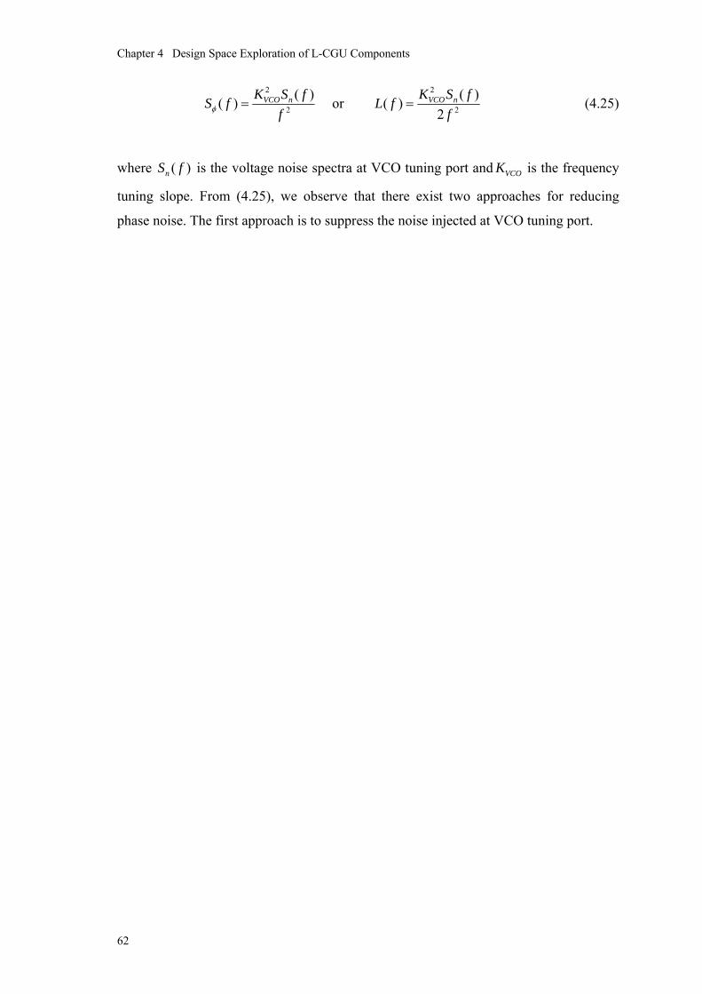
Chapter 4 Design Space Exploration of L-CGU Components
62
2
2
( )( ) VCO nK S fS ffφ = or
2
2
( )( )2
VCO nK S fL ff
= (4.25)
where ( )nS f is the voltage noise spectra at VCO tuning port and VCOK is the frequency
tuning slope. From (4.25), we observe that there exist two approaches for reducing
phase noise. The first approach is to suppress the noise injected at VCO tuning port.
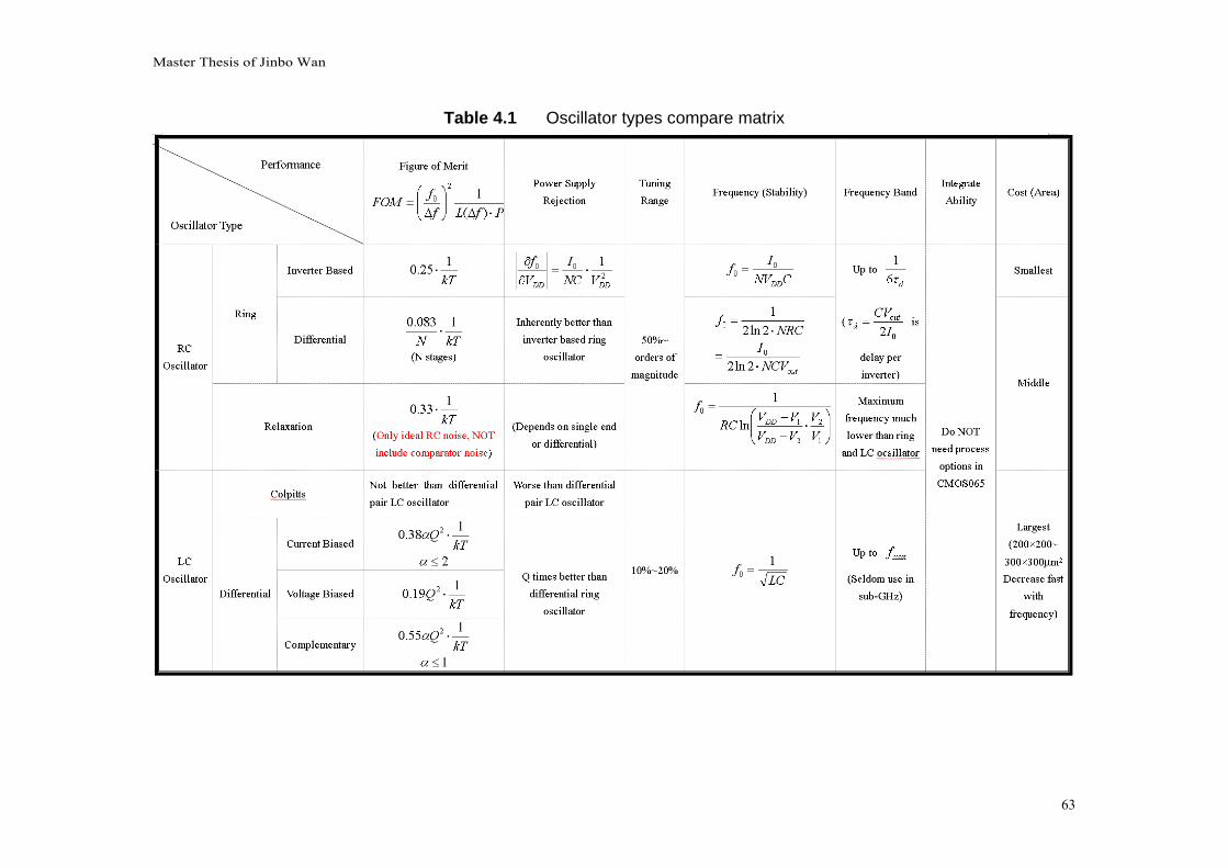
Master Thesis of Jinbo Wan
63
Table 4.1 Oscillator types compare matrix

Chapter 4 Design Space Exploration of L-CGU Components
64
This may require significant design effort and complexity, especially in the presence of
PSN. Another way to reduce the phase noise is lowing VCOK . This approach is more
robust because it does not require the suppression of noise, but it needs more considera-
tion on how to cover the whole frequency range. For the L-CGU we use the latter ap-
proach which will be shown in more detail in Section 5.2.2 of the next chapter.
4.3.2. Frequency Divider The frequency divider (FDIV) reduces a high input frequency to a lower one. The divi-
sion ratio can be an even number, an integer or even a fractional number. Ideally, the
FDIV does not add noise to its output signal. Moreover, it is capable of even reducing
the phase noise that is present in its input signal. Next, we will discuss the FDIV jitter
and phase noise characteristics. For this purpose, we make use of the phase model of
FDIV is shown in Figure 4.3.
Figure 4.3 Frequency divider phase model
inout
ffN
= , inout N
φφ = , __ 2
( )( ) in
out
S fS f
Nφ
φ = (4.26)
The FDIV output jitter can be obtained from both the white PM phase noise and white
FM phase noise (see section 3.3). For the white PM phase noise (noise floor), the FDIV
output jitter is 2
_ _2_ _ _2 2 2 2
( )1 1 1 1( ) ( )4 4 4
in in PMout PM out in
out in in
S f JJ S f S f
f N f N N f Nφ
φ φπ π π= ⋅ = ⋅ = ⋅ = (4.27)
For the white FM phase noise (-20dBc per decade part), the FDIV output jitter is 2 2 2
_2 2_ _ _ _3 2 3 3 3
( )( ) ( )
2 2 2in
out FM out in in FMout in in
S ff f fJ S f N S f N Jf N f N f
φφ φ= ⋅ = ⋅ = ⋅ ⋅ = ⋅ (4.28)
The total FDIV output jitter is found by taking the mean square sum of these two parts.
The strict analysis of the FDIV phase noise and jitter is complicated because of different
1/Ninfin
outffN
=
inφ inout N
φφ =

Master Thesis of Jinbo Wan
65
possible FDIV implementations. Commonly, the approach is to first calculate the output
noise voltage at the switching threshold and divide it by the voltage slope at that point. 2
_1( ) 2 ( )out n fold
out
S f f S fdv dtφ π
⎡ ⎤= ⎢ ⎥⎣ ⎦
(4.29)
22 12 var[ ( )]
out
J n iTdv dt⎡ ⎤
= ⎢ ⎥⎣ ⎦
(4.30)
_var[ ( )] ( )2out
n foldfn iT S f= (4.31)
Expression (4.31) has been confirmed with Wiener-Khinchine theorem [4.7].
In practice, the FDIV will contribute to jitter and phase noise as a result of intrinsic and
extrinsic noise sources. Since the FDIV is a driven system, its phase noise can not influ-
ence the output frequency of the PLL. The FDIV noise will only convert to the white
PM phase noise, e.g., it increases the phase noise floor. Fortunately, the FDIV phase
noise can be reduced using re-synchronization. The output signal of the FDIV is re-
synchronized with the FDIV input signal, which reduces any phase noise degradation
due to the FDIV. An example of re-synchronization is shown in Figure 4.4.
a) Asynchronous FDIV
b) Resynchronized FDIV

Chapter 4 Design Space Exploration of L-CGU Components
66
Figure 4.4 Re-synchronization for a Frequency Divider For an asynchronous FDIV, the noise of each stage is accumulated and the FDIV output
signal will contain this accumulated noise. A resynchronized FDIV can remove the
accumulated noises by using resynchronized D flip-flop. As a result, the FDIV output
noise will only contain the noise of the D flip-flop, and significant noise reduction is
achieved. One should make the FDIV delay without resynchronization smaller than half
of the input period (T/2). Otherwise, the circuit may become unstable after adding a
resynchronized D flip-flop.
In this work we will focus on programmable integer number FDIV. The design details
will be provided in the next chapter.
4.3.3. Phase Frequency Detector and Charge Pump The phase frequency detector (PFD) compares the phase difference of a reference and
feedback signal. It produces pulse output signals (up and down), whose pulse widths are
proportional to the phase difference. The PFD does not continuously monitor the phase
difference, but only compares the phase at the rising (or falling) edge of the inputs. In
this respect, the circuit operation may cause pulse width and timing mismatch issues at
its output. The charge pump (CP) converts the PFD output signals to a current output.
This output will be immediately passed to a low pass filter that is designed to suppress
signals at frequencies of 1/T and above. In most cases the pulsed nature of this signal
can be ignored in favor of its average value, cpi . The transfer function of the com-
bined PFD-CP is
det ( ) ( )2 2 2
cp cpcp ref fd ref fd error
I IKi φ φ φ φ φπ π π
= − = − = (4.32)
The logic model and phase model of PFD-CP is shown in Figure 4.5.
Next, we analyze the noise contribution of the PFD-CP. The intrinsic and extrinsic
noises of PFD add jitter to its outputs, which in their turn add disturbance to the pulse
width and timing of up down signal. This disturbance will affect the CP output cpi ac-
cordingly, which then converts to voltage noise through low pass filter and finally adds

Master Thesis of Jinbo Wan
67
to the control port of VCO. Now suppose the transfer function of the low pass filter
is ( )LFZ f . Then the phase noise due to PFD-CP output current cpi is
22
2( ) ( ) ( )cp
VCOi LF
KS f S f Z ffφ = (4.33)
Figure 4.5 The logic model and phase model of PFD-CP
The PFD-CP jitter and phase noise is caused by two effects. The first effect is because
of random noise and PSN, which produces a continuous phase noise in the PLL. Fortu-
nately, this contribution can be neglected because the charge pump is closed most of the
time when the PLL is locked. The second effect is because of the spurious signals in the
PLL output produced by the CP output current. This is the main jitter contribution to the
jitter on which we will focus our analysis. The spurs show themselves at reference
frequency reff and its harmonics, which are called reference spur. An illustration is
shown in Figure 4.6.
There are two sources which produce reference spur. The first source is the noise pro-
duced by other components of PLL that modulate the phase error. The modulated phase
error will modulate the PFD-CP current and generate reference spur. Figure 4.7 illus-
trates the cpi pulse sequences generated by noise in PLL. The detail analysis is made in
the book of Keliu Shu et.al [4.8].
The second source that produces the reference spur is the mismatch inside the PFD-CP.
a) Logic model of PFD-CP b) Phase model of PFD-CP

Chapter 4 Design Space Exploration of L-CGU Components
68
The following analysis will assume no phase error input to PFD-CP for acquiring in-
sight in the reference sour contribution to the phase noise. Figure 4.8 illustrates the
PFD-CP output current in one reference period refT due to non-idealities of the charge
pump.
Figure 4.6 Spurs in output frequency spectrum [4.7]
Figure 4.7 Charge-pump output current in locked state due to noise [4.8]
Since the PFD-CP output current outi is a periodic signal with period of refT , it can be
decomposed into a discrete Fourier series
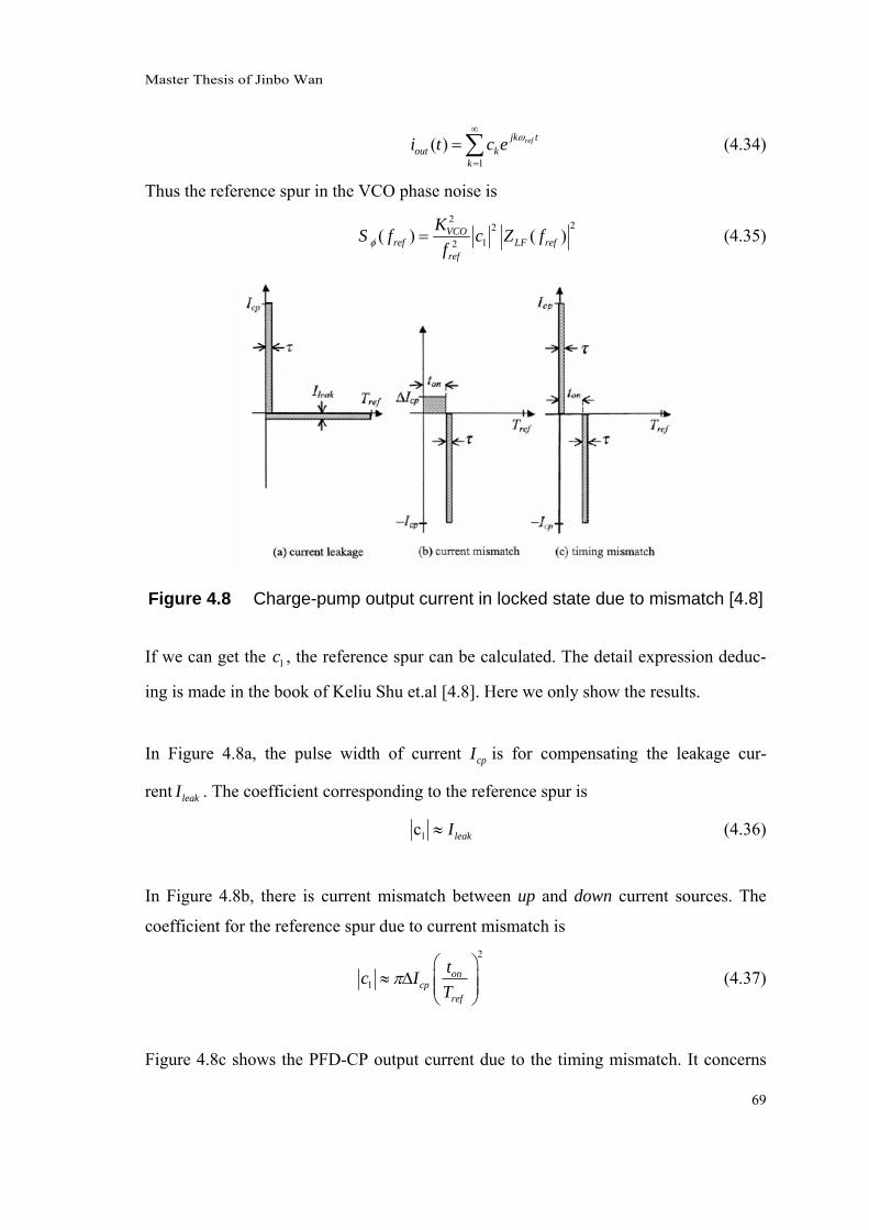
Master Thesis of Jinbo Wan
69
1( ) refjk t
out kk
i t c e ω∞
=
=∑ (4.34)
Thus the reference spur in the VCO phase noise is 2 22
12( ) ( )VCOref LF ref
ref
KS f c Z ffφ = (4.35)
Figure 4.8 Charge-pump output current in locked state due to mismatch [4.8]
If we can get the 1c , the reference spur can be calculated. The detail expression deduc-
ing is made in the book of Keliu Shu et.al [4.8]. Here we only show the results.
In Figure 4.8a, the pulse width of current cpI is for compensating the leakage cur-
rent leakI . The coefficient corresponding to the reference spur is
1c leakI≈ (4.36)
In Figure 4.8b, there is current mismatch between up and down current sources. The
coefficient for the reference spur due to current mismatch is 2
1on
cpref
tc IT
π⎛ ⎞
≈ ∆ ⎜ ⎟⎜ ⎟⎝ ⎠
(4.37)
Figure 4.8c shows the PFD-CP output current due to the timing mismatch. It concerns

Chapter 4 Design Space Exploration of L-CGU Components
70
timing mismatch between the falling edges of up and down, which causes both a posi-
tive and negative current pulse cpI with a pulse width equal to the timing mismatch.
The coefficient for the reference spur due to the timing mismatch is
1 2 oncp
ref ref
tc IT Tτπ≈ (4.38)
Besides the three kinds of mismatches as discussed above, the mismatches of clock
feed-through and charge sharing of up and dn switches also contribute to the reference
spur. Sometimes, dummy switches are used to reduce clock feed-through and charge
sharing.
Note that in a PLL with on-chip loop filter and VCO, the reference spur can be partially
contributed by the periodic PSN due to the periodic operation of the PFD, charge-pump
and loop divider.
4.3.4. Loop Filter
In a PFD-CP PLL, the loop filter (LF) is a kind of trans-impedance. An example of the
common structure is shown in Figure 4.9. The resistance and capacitance values are
calculated based on the required PLL loop bandwidth and phase margin.
Figure 4.9 Loop filter in a PFD-CP PLL
Normally, the capacitance values are very large which leads to a large LF layout area.
The noise from ground and substrate can be coupled to the LF output very easily. See
one simulation result example in figure 4.10. Since the LF output is directly connected
to VCO tuning port, such noise coupling would degrade the jitter and phase noise per-
formance. In this work, substrate shielding is not an option because the ground is shared

Master Thesis of Jinbo Wan
71
with digital blocks. The only viable way to reduce this noise coupling effect is to reduce
the VCO tuning slope VCOK .
With gnd noise
With Vdd noiseNo noise
Figure 4.10 Simulation result for the LF output at the condition of no noise, with Vdd noise and with gnd noise.
4.4. Summary In this chapter, we present our L-CGU solution. The L-CGU is based on an integer-N
PLL. The most important part in the L-CGU is the oscillator. In order to find the suit-
able oscillator type for the L-CGU application, seven different kinds of oscillators are
compared in phase noise, power consumption, area, power supply sensitivity, and inte-
gration capability. The two suitable oscillator types are chosen as the core for the L-
CGU. In the following sections, the jitters under power supply noise of clock buffer,
frequency divider (FDIV), phase frequency detector and charge pump (PFD-CP), loop
filter (LF) are analyzed. Next chapter we will show the detail design of the L-CGU,
which include both schematics and layouts.

Chapter 4 Design Space Exploration of L-CGU Components
72
Reference [4.1] M. Meijer, Pessolano, J.Pineda de Gyvez, “Glitch-Free Discretely Programma-
ble Clock Generation on Chip,” IEEE International Symposium on Circuits and
Systems, 1839 – 1842, May 2005.
[4.2] P. Kinget, “Integrated GHz Voltage Control Oscillators,” in Analog Circuit
Design: (X)DSL and other Communication Systems; RF MOST Models; Inte-
grated Filter and Oscillators, W. Sansen, J Huijsing, and R. van de Plassche,
Eds Boston: Kluwer, 353-381, 1999,
[4.3] A. A. Abidi, “Phase Noise and Jitter in CMOS Ring Oscillators,” IEEE Journal
of Solid-State Circuits, vol. 41, no. 8, 1803-1816, Aug. 2006.
[4.4] M. Lax, “Classical noise. V. Noise in self-sustained oscillators,” Phys. Rev., vol.
160, no. 2, 291–307, 1967.
[4.5] R. Navid, Thomas H. Lee, R. W. Dutton, “Minimum Achievable Phase Noise of
RC Oscillators,” IEEE Journal of Solid-State Circuits, vol. 40, no. 3, 630-637,
Mar. 2005.
[4.6] E. Hegazi, J. Rael, A. A. Abidi, The Designer’s Guide to High-Purity Oscilla-
tors, New York: Kluwer, 2005.
[4.7] A. Papoulis and S. U. Pillai, Probability, Random Variables, and Stochastic
Processes, New York: McGraw Hill, 2002.
[4.8] K. Shu et. al., CMOS PLL Synthesizers - Analysis and Design, Boston: Springer,
2005.

Master Thesis of Jinbo Wan
73
5. L-CGU Design So far we have discussed the requirements for the L-CGU. A detailed analysis has been
performed on the most critical requirement, namely the jitter performance when operat-
ing from a digital ‘noisy’ supply. In this chapter we will present the L-CGU schematic
designs and layouts implemented in a 65nm low-power CMOS technology. The simula-
tion results that are shown in this chapter are based on SpectreTM circuit simulations
using extracted layouts. The supply voltage for all circuits is 1.2V and can tolerate ±
10% variations (1.08V~1.32V).
5.1. L-CGU System Architecture The L-CGU is based on an integer-N PLL which produces all the required clock frequen-
cies and control functions such as, e.g. frequency transitioning, clock gating and clock
enabling. Control logic is used to provide an easy way for monitor and control the PLL
working conditions. Since the working condition of the L-CGU is determined by the
application, the control logic may be different from power domains to power domains.
Normally the control logic will be designed by the system engineer who what to use the
L-CGU. So in this thesis, only the integer-N PLL of the L-CGU is introduced. The con-
trol logics used in the thesis test chip are just some scan chain registers. Figure 5.1 shows
a general block diagram of the L-CGU.
Integer-N PLL
Control logic
out
L-CGU
Figure 5.1 General block diagram of the L-CGU
Figure 5.2 shows a block diagram of the integer-N PLL. The basic components are the

Chapter 5 L-CGU Design
74
voltage-controlled oscillator (VCO), phase-frequency detector (PFD), charge pump (CP),
loop filter (LF), frequency dividers (FDIV), and a lock detector.
Figure 5.2 Integer-N PLL structure
The PLL output frequency, fout, is N M times the reference frequency fref.
refVCOout
N fffM M
⋅= = (5.1)
In this work, we use a 26MHz reference frequency that is commonly available in mobile
systems, and generated by a crystal oscillator. Since fout is a multiplication of fref, the
clock output frequencies are slightly shifted from the requirements shown in Table 2.1.
The PLL output frequencies for given frequency divider settings are shown in Table 5.1.
Table 5.1 PLL output frequencies and divider numbers
Frequency[5.MHz] 48.75 97.5 156 195 247 312 338 390 442 494 546
N 15 15 12 15 19 12 13 15 17 19 21
M 8 4 2 2 2 1 1 1 1 1 1
As compared to conventional integer-N PLLs, our integer-N PLL differs on two parts.
The first one is the VCO design which is the most critical part in the PLL; it should
generate a robust oscillation frequency insensitive to supply noise. We consider two
types of VCO designs: 1) a differential ring-oscillator VCO, and 2) a differential LC
VCO. In the course of this work we have designed two differential ring-oscillator VCOs
and one differential LC VCO. The second part is the Lock Detector. Lock Detector
reff
fdf
up
down
cpi tunev
VCOf outf
NPE
Lock
CP
LF
VCOPFD
FDIV MFDIV N
Lock Detector C
ontro
l
Con
trol
5 2

Master Thesis of Jinbo Wan
75
which is used to monitor the PLL status during frequency transitioning. It produces two
output signals: no phase error (NPE) and Lock, which will be explained in section 5.7.
The PLL is a 3th-order type II charge pump PLL. To make the PLL loop stable, its loop
bandwidth cf is set to be tenth of the reference frequency: 2.6MHz.
11
1 2
2.62 10cp VCO ref
c
I K fCf R MHzN C Cπ
= = =+
(5.2)
In (5.2), cpI is the charge pump current. VCOK is the VCO tuning sensitivity in (Hz/Volt).
1R , 1C and 2C are the components value in the loop filter (LF). The normalized third
pole is set to be 9 to get fast lock [5.1].
2
3
9b ττ
= = (5.3)
where 2τ is the time constant of the “stabilizing” zero, and 3τ is the time constant of the
pole which is used to attenuate the reference frequency and its harmonics. They will be
discussed in Section 5.6.
In order to get the maximum phase margin, the normalized loop bandwidth is set to be 3.
2' 2 3cK f bπ τ= = = (5.4)
This gives a phase margin of53° [5.2].
5.2. Voltage Control Oscillator The VCO determines most of the PLL performance, such as jitters, clock frequencies,
power consumption, and the area occupation. We have developed three different VCO’s
for trading-off L-CGU characteristics and comparison purposes. The design has been
started with a differential ring-oscillator VCO, and a differential LC VCO. Later, we
have improved the differential ring-oscillator VCO, and have developed a third VCO.
Each VCO has been used to design and implement a PLL in 65nm CMOS. Next, we will
discuss the different VCO designs in detail.

Chapter 5 L-CGU Design
76
5.2.1. Differential ring-oscillator VCO Figure 5.3 shows a simplified block diagram of the differential ring-oscillator VCO. Its
oscillation frequency ranges from 624MHz up to 1092MHz. The Ring-VCO output
frequency is divided by 2 to guarantee 50% duty cycle at the VCO output. Finally, the
VCO output frequency ranges from 312MHz up to 546MHz.
RingVCO ÷2
VCO part
648~1092MHz
324~546MHz
Figure 5.3 Structure of the differential ring-oscillator VCO
5.2.1.1 Schematics design for differential ring-oscillator VCO
The implemented differential ring-oscillator VCO is based on the famous design of John
G. Maneatis [5.3]. The delay cells in the ring-oscillator use symmetric loads as tuning
resistors. The two tuning voltages, which tune the symmetric load PMOS and tail current
source, are generated from replica bias. The sine-wave shaped output amplitude of the
delay cell is impacted by the tuning voltage, and is not suitable as ring-VCO output.
Therefore, a high gain buffer for generating a full voltage swing square wave. We refer to
[5.3] for the detailed design considerations. Figure 5.4 shows the top-level circuit sche-
matic of the differential ring-oscillator VCO. It consists of three delay stages, a replica
bias circuit and an output buffer. The circuit schematics of the replica bias, differential
delay cell, and output buffer are shown in Figure 5.5, Figure 5.6, and Figure 5.7, respec-
tively.

Master Thesis of Jinbo Wan
77
Figure 5.4 Top level schematic of the differential ring VCO
Figure 5.5 Replica bias for tuning the VCO
Figure 5.6 Differential delay cell with symmetric load
Replica Buffer 3 stages differential delay cells

Chapter 5 L-CGU Design
78
Figure 5.7 VCO output buffer
One difference from [5.3] is that we add fixed capacitors to each differential delay cell.
By using fixed capacitors, the influence of parasitic capacitances is reduced, which in its
turn reduces the sensitivity to the power supply noise. To maximize the capacitance value
of these capacitances, the number of the delay stages is set to a minimum of 3 stages.
The tail current for each delay cell is setting by the replica bias and in sequence con-
trolled by the tuning voltage. So there is only one current which required to be biased
outside. It is the bias current for the differential amplifier within the replica bias, which
named “Ibias”. The normal current for “Ibias” is 45μA. Yet it needn’t to be very accu-
rate. Current from 20μA to 70μA are all acceptable.
The power consumption of the differential ring-oscillator VCO is variable with output
frequency. When operates at its highest required frequency 1.092GHz and fabricates at
nominal process corner, the total current for the VCO is around 800μA.
5.2.1.2 Layout for differential ring-oscillator VCO
The layout design has a large impact on the final circuit performance. A badly designed
layout increases the circuit parasitics, lowers the maximum operating frequency, worsens
the noise coupling and makes the circuit mismatch unbalanced. Therefore, it is of prime

Master Thesis of Jinbo Wan
79
importance that the layout is carefully designed for achieving a good performing circuit.
All differential transistor pairs make use of a common-centroid layout organization to
ensure proper matching of transistor pairs [5.4].
The layout of the differential ring-oscillator VCO is shown in Figure 5.8. The layout
consists of three parts. The bottom part is the replica bias, which processes the tuning
signal from the LF output. The top part is the VCO output buffer that converts the differ-
ential output of the ring-oscillator to a full-swing square wave signal. The middle part
consists of three differential delay cells that constitute the ring-socillator. Their layout is
stacked to make a symmetrical ring-oscillator layout. So any coupling noise will mostly
convert to common mode noise. However, such layout configuration will make the wire
connections among the delay cells unequal in length. Moreover, the output buffer is
connected with the upper delay cell. This makes the delay cells to be not equally loaded,
and the phase is not divided in exactly 120 degrees. Since we do not care about the phase
at the VCO output, this layout configuration is acceptable.
The whole VCO layout is made to be as symmetrical as possible. Each transistor group is
surrounded with a guard ring. The whole VCO is surrounded with power ground rings
together with a big guard ring. The power and ground connections are made large in
width (about 1µm) to reduce the resistance in the power ground networks. The area for
the differential ring-oscillator VCO is 18μm×48μm.
5.2.1.2 Simulations for differential ring-oscillator VCO
The VCO tuning range is found to be very large, e.g. from several tens of MHz to about
1.2GHz. Figure 5.9 shows the simulation results of the oscillation frequency versus
tuning voltage. A tuning voltage has been applied from 0V up to 0.9V. The different
lines indicate the results from five process corners: fnfp (purple), fnsp (blue), nominal
(red), snfp (yellow), and snsp (light blue). The lines saturate for tuning voltages lower
than 0.2V because the “vbp” output of replica bias (see Figure 5.5) can not follow the
change of tuning voltage anymore.

Chapter 5 L-CGU Design
80
Buffer
3 stage delay cells
Replica bias tuning
Figure 5.8 Layout of the first differential ring-oscillator VCO
Power ring, ground ring and guard ring. They are stacked

Master Thesis of Jinbo Wan
81
Figure 5.9 Simulation results of oscillation frequency versus tuning voltage of the differential ring-oscillator VCO for various process corners
Figure 5.10 shows the simulated phase noise without any power supply noise. Figure
5.11 shows the simulated phase noise while applying white power supply noise accord-
ing to our model shown in Section 3.4 using noise spectrum amplitude of about 1.23E-
12 2V Hz . A comparison of Figure 5.10 and Figure 5.11 shows that the phase noise
becomes more than 30dB worse when power supply noise is present. While including the
divide-by-2 frequency divider, we calculated the RMS jitter of the VCO at 546MHz. We
observed a jitter of 3ps in case of no power supply noise, while the jitter with power
supply noise is 108ps! Such large jitter cannot be tolerated for the L-CGU design.

Chapter 5 L-CGU Design
82
Figure 5.10 Phase noise of the differential ring-oscillator VCO at 1092MHz, no power supply noise. RMS period jitter (at 546MHz): 3ps
Figure 5.11 Phase noise of the differential ring-oscillator VCO at 1092MHz, with power supply noise added. RMS period jitter (at 546MHz): 108ps

Master Thesis of Jinbo Wan
83
5.2.2. Reduce the jitter of the VCO under large power supply noise In order to find the root cause of the large jitter in case of power supply noise, we ana-
lyzed the differential ring-oscillator VCO in more detail. The phase noise induced by
power supply noise can be expressed as follows,
( ) ( )2
22Vdd
VddKL f S f
f= (5.5)
( )VddS f is the power supply noise spectrum. VddK is the sensitivity of the VCO output
frequency to the power supply variation. ( )VddS f can not be lowered easily in this pro-
ject, because not only the power supply of the L-CGU is shared with digital IP blocks,
but also the L-CGU itself is totally embedded in the digital circuits. So the only way to
reduce the phase noise is to reduce the frequency sensitivity VddK . In fact, there are at
least three ways to reduce the VCO sensitivity to power supply noise.
The first way is through balancing the load resistors. The power supply noise directly
couples to the delay cell output through the load resistors (see Figure 5.12). Since this
noise is common mode, it can greatly rejected by the next delay stage when the circuit is
fully symmetric. However, mismatch may occur in the symmetric load PMOS pair,
which makes their equivalent resistance not equal at all times. This makes common mode
rejection ratio (CMRR) poor, and VddK is influenced.
Figure 5.12 Power supply noise coupling to the output through load resistors

Chapter 5 L-CGU Design
84
The second way is to reduce the power supply controlled parasitics. The VCO oscillation
frequency is determined by the RC time constant of the delay cell. By making the RC
time constant insensitive to power supply, the VddK can be reduced. When fixed load
resistors and fixed capacitors are used, the parasitic capacitance change seen at the delay
cell differential output changes because of a change in DC bias point (see Figure 5.13).
Such change in DC bias point can reduced if the fixed resistance and fixed capacitance
values dominate the parasitic ones. Moreover, a large tail current source impedance can
also help to reduce VddK .. Unfortunately, there is not much voltage headroom for a stack
of three transistors in case of the delay cell shown in Figure 5.6. Consequently, the tail
current source operates close to the triode region, and its output impedance is not large.
Also, symmetric load PMOS pairs add parasitic capacitances.
Figure 5.13 Parasitics seen at the differential output of the delay cell
The third way to reduce the VCO sensitivity to power supply noise is by accurate voltage
control. In a differential ring VCO, the frequency tuning is realized through voltage
control components, such as voltage control resistors or varactors. The value of such
components is determined by the voltage apply at the tuning port and the voltage at the
reference port. Normally the reference port is biased at a fixed DC value. Yet when
power supply varies, the reference port no longer fixed any more. It is equal to applying a
tuning voltage at the voltage control component. And as a result, the frequency will
change with respect to the varying of the power supply. For example, in Figure 5.14,
suppose the frequency is controlled by varactors. Then vout+ and vout- are reference

Master Thesis of Jinbo Wan
85
ports. When Vdd changes, the DC bias voltages at vout+ and vout- are changed accord-
ingly. It’s equal to tuning the varactors, although the voltages applied at tuning ports are
not varied. Based on the above discussion, an immediate observation can be made: the
larger the VCO tuning sensitivity VCOK , the larger the power supply sensitivity VddK .
Wide tuning VCOs often have poor phase noise performance when the power supply is
noisy. In the designed a differential ring VCO, the tuning range is wide and VCOK is very
large (about 3.3GHz/V). Moreover, the replica bias will induce some power supply noise
to the tuning port. So the phase noise is very bad when we add power supply noise.
Figure 5.14 Reference ports of the tuning components influenced by power supply noise
5.2.3. Improved differential ring-oscillator VCO Based on the previous observations, we have designed an improved differential ring-
oscillator VCO. Figure 5.15 shows a schematic diagram of its delay cell. We use a spe-
cial capacitor tuning instead of resistor tuning; a number of small tuning varactors are
connected in parallel with a switchable large fixed capacitor tank. This lowers the influ-
ence of parasitic capacitances at the differential output nodes. Moreover, we use fixed
polysilicon resistor loads. This provides better load resistor balancing and high CMRR
for power supply noise. Also, it increases the voltage head room for the tail current
source, which can now operate strong inversion to increase its output impedance.

Chapter 5 L-CGU Design
86
Figure 5.15 Sketched circuit for the improved differential ring VCO delay cell
5.2.3.1 Schematics design for the improved differential ring-oscillator VCO
Figure 5.16 shows the top-level schematic of the improved differential ring-oscillator
VCO. The two footer NMOS transistors are for bias and shutdown purpose. The circuit
schematic of the differential delay cell is shown in Figure 5.17. The VCO output buffer is
the same as shown in Figure 5.7.
Figure 5.16 Top level schematics for improved differential ring VCO
Unlike the previous differential ring-oscillator VCO, the tail current for each delay cell is
constant and does not change with the VCO operating frequency. The outside applied

Master Thesis of Jinbo Wan
87
bias current (through “Ibias”) is 30μA. Under this bias setting, the tail current for each
delay cell is 100μA. The bias current range for “Ibias” is from 20μA to 40μA.
The total current consumption of the improved differential ring-oscillator VCO is around
550μA.
Figure 5.17 Schematic circuit for the delay cell of the improved VCO
5.2.3.2 Layout for the improved differential ring-oscillator VCO
Figure 5.18 shows the layout of the improved differential ring-oscillator VCO. The
layout structure is similar to Figure 5.8 except the replica bias which is not needed. The
VCO output buffer is the same as used before. Some decoupling capacitors are used to
fill in the space at both sides of the buffer. The delay cells of the improved differential
ring-oscillator VCO are larger as compared to the previous ones. This is because the
fixed metal capacitors in the tuning tank are larger (45fF compare to 10fF). Between
these metal capacitors, some space should be kept to reduce the direct coupling, other-
wise the VCO oscillation frequency will reduce and the switches in the tuning tank will

Chapter 5 L-CGU Design
88
loose their effect. Moreover, power and ground rings are used to surround each delay cell.
They can reduce the direct coupling between delay cells through the edges of the big
metal capacitors. The whole layout of the improved differential ring VCO is designed to
be fully symmetrical, and the area is 55μm× 42μm.
Figure 5.18 Layout of the improved differential ring-oscillator VCO
5.2.3.3 Simulations for the improved differential ring-oscillator VCO
The simulated frequency tuning range and phase noise are shown in Figure 5.19 and
Figure 5.20, respectively.
Again, we calculated the RMS period jitter after the divide-by-2 frequency divider using
the same method as before, e.g. the jitter at 546MHz VCO output. We observed a jitter
of 2.1ps in case of no power supply noise, while the jitter with both power and ground

Master Thesis of Jinbo Wan
89
Figure 5.19 Simulated frequency tuning range at nominal process corner
Figure 5.20 Simulated phase noise at 1.092GHz under no power supply noise, only power noise and only ground noise situations

Chapter 5 L-CGU Design
90
noise is 7.4ps. We conclude that the improved differential ring-oscillator VCO is much
better than old one.
The drawbacks of the improved differential ring VCO is the larger area cost and the need
of initial calibration. From the simulation result show in Table 6.1 of Chapter 6, we see
that the frequency range of the improved differential ring-oscillator VCO is limited, and
does not cover the basic requirement, i.e. 624MHz up to 1092MHz for all process cor-
ners. One solution to this problem is to redesign this VCO and add another switch capaci-
tor pair to the tuning tank to enlarge the frequency range. However, adding such capaci-
tor pair will increase the circuit area significantly because of the large required capaci-
tance value. Moreover, the maximum VCO frequency will be reduced due to the large
parasitic capacitive loading. Another solution is to increase the tuning varactor value to
cover more frequency range. Unfortunately, this will increase KVCO, which in its turn,
will degrade the VCO jitter performance. We do not use follow this solution, but rather
we use a calibration approach to solve this problem. The calibration approach of the
improved differential ring VCO based PLL is shown in Appendix 5B.
5.2.4. LC VCO part The second type of L-CGU is based on an LC VCO. We developed an LC VCO based
PLL for test and comparison purposes against the differential ring-oscillator based PLLs.
Figure 5.21 shows a simplified block diagram of the LC VCO. A high-frequency fre-
quency divider (FDIV X) has been designed allowing the VCO to operate at an oscilla-
tion frequency in between 3.9GHz and 4.42GHz with a small tuning range (of about
12%). Table 5.2 shows the relation of the frequency divider number, X, and the VCO
output frequency.
Figure 5.21 LC VCO part structure

Master Thesis of Jinbo Wan
91
The design of the frequency divider (FDIV X) will be discussed in section 5.3.
Table 5.2 Frequency plan for LC VCO and the divider number of FDIV X Output frequency [5.MHz] 312 338 390 442 494 546
LC-VCO frequency [5.MHz] 4368 4056 3900 4420 3952 4368
X 14 12 10 10 8 8
5.2.4.1 Schematics design for the LC VCO
Figure 5.22 shows the toplevel schematic of the LC VCO. The circuit details of the LC
VCO and the output buffer are shown in Figure 5.23 and Figure 5.24, respectively. The
LC VCO is implemented as a complementary LC oscillator. The varactor is implemented
as NMOS in Nwell for biasing the device in the depletion region or accumulation region
only. The varactor can achieve a very wide tuning range, because its reference port is
biased at about VDD/2. Moreover, the oscillator voltage swing is limited in between 0 and
VDD which enables a reliable operation in a 65nm low-power CMOS technology. We
make use of two control signals (switch0 and switch1 in Figure 5.22, and Figure 5.23) for
frequency calibration purposes. The reason for such calibration is because the inductor
model provided in the technology library may not be very accurate. In the final imple-
mentation, the use of these calibration signals and the associated capacitor tanks may be
discarded.
Figure 5.22 Top level schematic of the LC VCO

Chapter 5 L-CGU Design
92
Figure 5.23 Circuit schematic of the LC VCO
Figure 5.24 Circuit schematic of the VCO output buffer

Master Thesis of Jinbo Wan
93
The buffer shown in Figure 5.24 has two functions. First, it isolates the VCO and the
FDIV X which followed the VCO. Second, it converts the dc bias of the VCO output (0V)
to the require level by the FDIV X (0.8V). For the isolation function, two small capaci-
tors (10fF) are used at the input of the buffer. They will largely reduce the influence from
the output buffer to the VCO, and achieve very good isolation. At the same time, the
small capacitors serials in the signal route will reduce the amplitude of the VCO output
signals, which will increase the noise floor. Yet the increase of the noise floor will not be
found because it is overwhelmed by the large power supply noise. For the bias level
converting, the buffer used the similar circuits, the same components values, and same
bias current with the FDIV X, together with negative DC feed back.
There are two outside bias pins for the LC VCO. One for oscillator core (“Itail”) and the
other for the buffer (“Ibuffer”). Normally, the bias current for “Itail” is 40μA, and
“Ibuffer” is 50μA. Under these bias currents, the tail current of the complementary LC
oscillator is 350μA, and the tail current for each differential stage in the buffer is 150μ
A. The bias range for “Itail” is from 30μA to 80μA, and the bias range for “Ibuffer” is
from 45μA to 80μA. The total current consumption of the LC VCO (include the buffer)
is around 750μA.
5.2.4.2 Layout for the LC VCO
Figure 5.25 shows the layout of the LC VCO. This is the biggest VCO due to the need of
a spiral inductor. We used a “0” shaped inductor which was supported in the technology
library. The spiral inductor use three top layer (metal 6, metal 7 and AP) with inner
diameter 60μm, line width 10μm, spacing 2.51μm and 5 loops. The inductance is
about 3.079nH with serial resistance about 1.64Ω. The differential floating shield induc-
tor we used in the layout may pick up some noise, which is difficult to simulate. Meas-
urement results should provide insight on this.
The LC VCO is surrounded by power and ground rings together with a big guard ring.
These rings are stacked and at least “5*W” (50μm) far from the inductor. Otherwise the

Chapter 5 L-CGU Design
94
magnetic coupling from the inductor to the rings will reduce the Q value of the resonate
tank. The power and ground rings are interrupted at the top centre to avoid the induced
loop current. The wire connections between the inductor to the oscillator circuit are made
by stacked metal layers, which can achieve both low resistance and low capacitance. The
whole layout is designed to be fully symmetrical. The area is about 360μm×325μm.
Figure 5.25 Layout of the LC VCO
5.2.4.3 Simulations for the LC VCO
Figure 5.26 illustrates the frequency range of the LC VCO at all possible calibrating
situations. Figure 5.27 and Figure 5.28 show the phase noise at the LC-VCO output at
4.368GHz for the case without and with power supply noise, respectively. We have
determined the RMS period jitter at VCO output at 546MHz. The jitter without power
supply noise is found to be about 0.2ps, while the jitter with power supply noise is found
to be about 10ps.

Master Thesis of Jinbo Wan
95
Figure 5.26 Frequency range at all calibration situations
Figure 5.27 LC VCO phase noise at 4.368GHz, no power supply noise

Chapter 5 L-CGU Design
96
Figure 5.28 LC VCO phase noise at 4.368GHz, with power supply noise
In this section, we have described three different VCO designs as developed in this work.
The first differential ring-oscillator VCO is easy to use and is smallest in area, but suffers
from the worst jitter performance under power supply noise conditions as compared to
the other VCO’s. The improved differential ring-oscillator VCO offers a very good jitter
performance, even under power supply noise conditions. However, it requires initial
calibration for process condition compensation and it is consumes more silicon area. The
LC VCO has the largest silicon footprint, and it consumes the most power consumption.
However, it is easy to use and offers a good jitter performance.
5.3. Frequency Divider (FDIV) In this section we will show the design of the three frequency dividers (FDIV M, FDIV
N, and FDIV X). The differential ring-oscillator VCO based PLL does not make use of
the FDIV X frequency divider.
5.3.1. Schematic designs of FDIV
The simplest frequency divider is FDIV M for which the circuit schematic is shown in

Master Thesis of Jinbo Wan
97
Figure 5.29. It divides the input clock frequency by a factor of 1, 2, 4, or 8 based on the
selection signal (see Table 5.3). The FDIV M output is re-clocked by the clock frequency
of two times the input one to get rid of the frequency divider jitter (the re-clocking is not
shown in Figure 5.29). Using the FDIV M input to re-clock its output will not work,
because the delay through the 4:1 MUX is simply too small when the FDIV M is set to
be divide-by-1. In this case, the re-clocking D flip-flop can not produce a stable output
signal when its data and clock input change at the same time.
Figure 5.29 Circuit schematic of the frequency divider FDIV M
Table 5.3 Divide number settings for FDIV M
p1 p0 Divider number 0 0 ÷1
0 1 ÷2
1 0 ÷4
1 1 ÷8
The FDIV N is realized by using a special programmable frequency divider structure, as
proposed by C. Vaucher [5.2] (shown in Figure 5.30). It is composed of a basic divide-
by-2/3 cell as shown in Figure 5.31. This kind of frequency divider can achieve very
wide divide range as well as a short propagation delay. Its division number can be set
from ÷8 to ÷31, thereby it fully covers the required divide range: ÷12, ÷13, ÷15, ÷
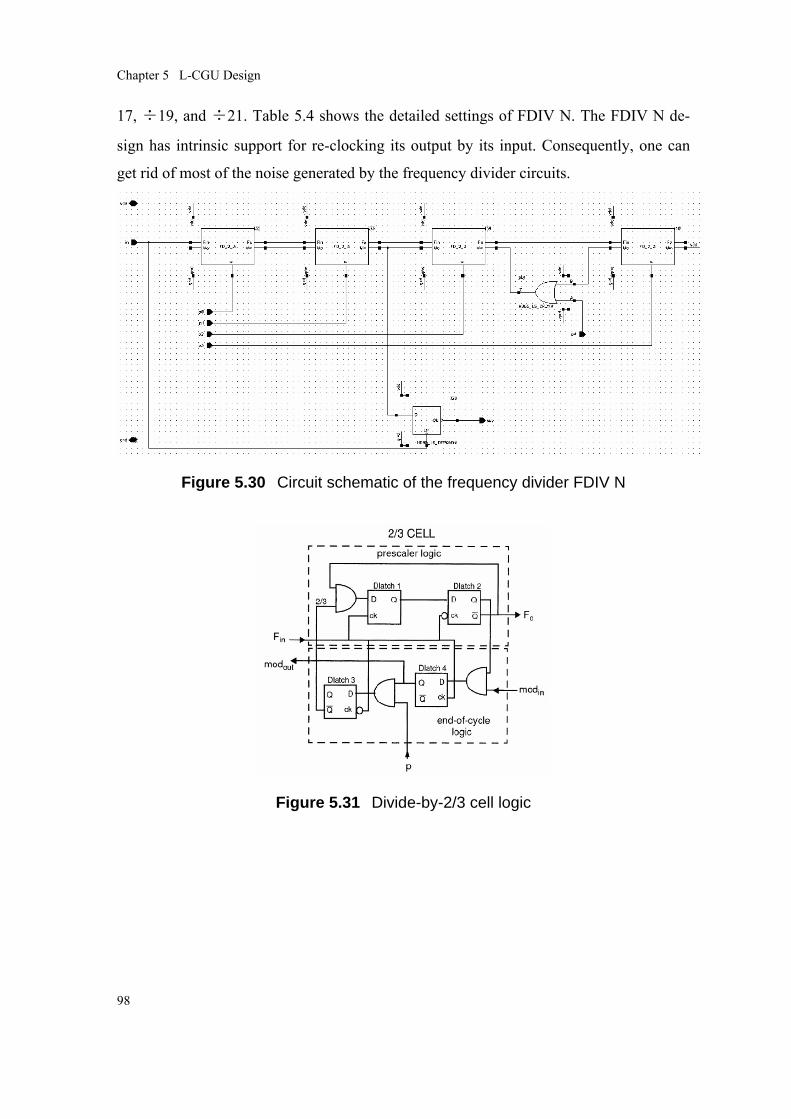
Chapter 5 L-CGU Design
98
17, ÷19, and ÷21. Table 5.4 shows the detailed settings of FDIV N. The FDIV N de-
sign has intrinsic support for re-clocking its output by its input. Consequently, one can
get rid of most of the noise generated by the frequency divider circuits.
Figure 5.30 Circuit schematic of the frequency divider FDIV N
Figure 5.31 Divide-by-2/3 cell logic

Master Thesis of Jinbo Wan
99
Table 5.4 Divide number settings for FDIV N
p4 p3 p2 p1 p0 Divider number
1 X 0 0 0 ÷8
1 X 0 0 1 ÷9
1 X 0 1 0 ÷10
1 X 0 1 1 ÷11
1 X 1 0 0 ÷12
1 X 1 0 1 ÷13
1 X 1 1 0 ÷14
1 X 1 1 1 ÷15
0 0 0 0 0 ÷16
0 0 0 0 1 ÷17
0 0 0 1 0 ÷18
0 0 0 1 1 ÷19
0 0 1 0 0 ÷20
0 0 1 0 1 ÷21
0 0 1 1 0 ÷22
0 0 1 1 1 ÷23
0 1 0 0 0 ÷24
0 1 0 0 1 ÷25
0 1 0 1 0 ÷26
0 1 0 1 1 ÷27
0 1 1 0 0 ÷28
0 1 1 0 1 ÷29
0 1 1 1 0 ÷30
0 1 1 1 1 ÷31
The FDIV X used by the LC VCO is based on the same concept as the FDIV N, but its
circuit implementation is different. Since the FDIV X input frequency could be higher
than 5GHz, it requires special high-speed circuits because conventional standard cell
circuits are speed-limited. The FDIV X makes use of Source Coupled Logic (SCL) cir-

Chapter 5 L-CGU Design
100
cuits, which offer such high frequency operation at the expense of power consumption.
Figure 5.32 illustrates the toplevel schematic of FDIV X. The first divide-by-2/3 cell
consumes full power (total tail current for the first divide-by-2/3 cell is 600μA) and
working at full speed (higher to 5GHz), while the second divide-by-2/3 cell consumes
only half power because its input frequency is only half of the first cell and can work at
lower speed.
Figure 5.32 Circuit schematic of the frequency divider FDIV X
Since the SCL logic output is a differential signal, a buffer is used for converting the
differential output to a single-ended full-swing square wave. A circuit schematic of this
buffer is shown in Figure 5.33.
Figure 5.33 The FDIV X buffer to convert a differential to single-ended output

Master Thesis of Jinbo Wan
101
One of the SCL D-latches with AND function is shown in Figure 5.34. A key point in the
design is to keep the loop gain of the cross-coupled pair large enough to ensure a stable
operation of the latch.
Figure 5.34 Source Coupled Logic D-latch combined with an AND function
The divide number settings of FDIV X are shown in Table 5.5. They include a divide-by-
2 D flip-flop for guaranteeing a 50% duty–cycle operation. This D flip-flop is located at
he FDIV X output and not shown in Figure 5.32.
Table 5.5 Divide number settings for FDIV X (including ÷2 stage, which is not shown in Figure 5.32 )
p1 p0 Divider number
0 0 ÷8
0 1 ÷10
1 0 ÷12

Chapter 5 L-CGU Design
102
1 1 ÷14
5.3.2. Layouts of FDIV
The FDIV M and FDIV N are composed of logic gates from the digital standard-cell
library. Their layout is straightforward, and does not require a symmetrical layout. This is
because is simply implements a given logic function which is operating at a relatively
low frequency. The layout of the FDIV M and FDIV N are shown in Figure 5.35 and
Figure 5.36 separately.
Figure 5.35 Layout of FDIV M
Figure 5.36 Layout of FDIV N

Master Thesis of Jinbo Wan
103
The FDIV X is used in the LC PLL only; its layout is shown in Figure 5.37. Like the
previous frequency dividers, the layout of FDIV X does not need to be symmetrical.
However, the main concern is to make the connections as short as possible for achieving
the required high-frequency operation. We designed the FDIV X to operate up to 6GHz
independent of the process corner.
Figure 5.37 Layout of the high-frequency divider FDIV X
The two connections in the differential pair in the FDIV X should be matched to ensure
the phase of the differential signals to remain the same. Another point of attention is the
folding of the MOS transistors in the SCL D-latches. The eight SCL D-latches are placed
symmetrically with respect to the vertical axis, i.e. towards right or towards left. For
proper matching, the MOS transistors should be insensitive to such placement. We have
solved this problem by folding the MOS transistors such they become centro-symmetric.
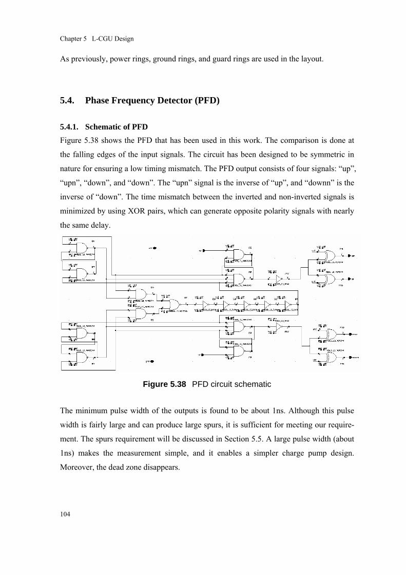
Chapter 5 L-CGU Design
104
As previously, power rings, ground rings, and guard rings are used in the layout.
5.4. Phase Frequency Detector (PFD)
5.4.1. Schematic of PFD Figure 5.38 shows the PFD that has been used in this work. The comparison is done at
the falling edges of the input signals. The circuit has been designed to be symmetric in
nature for ensuring a low timing mismatch. The PFD output consists of four signals: “up”,
“upn”, “down”, and “down”. The “upn” signal is the inverse of “up”, and “downn” is the
inverse of “down”. The time mismatch between the inverted and non-inverted signals is
minimized by using XOR pairs, which can generate opposite polarity signals with nearly
the same delay.
Figure 5.38 PFD circuit schematic
The minimum pulse width of the outputs is found to be about 1ns. Although this pulse
width is fairly large and can produce large spurs, it is sufficient for meeting our require-
ment. The spurs requirement will be discussed in Section 5.5. A large pulse width (about
1ns) makes the measurement simple, and it enables a simpler charge pump design.
Moreover, the dead zone disappears.

Master Thesis of Jinbo Wan
105
5.4.2. Layout of PFD The PFD is composed of logic gates from the digital standard-cell library. Its layout is
straightforward, but it is made symmetrical to minimize potential timing mismatch within
the circuit. The circuit is surrounded by power rings, ground rings, and guard rings. The
layout of the PFD is shown in Figure 5.39.
Figure 5.39 PFD layout
5.5. Charge Pump (CP) Most of the spurs in a PLL are generated by the charge pump. The largest spur is located
at the reference frequency (reference spur), and it has the biggest influence on the PLL
jitter performance. Therefore, the most important requirement for the CP design is the
reference spur level. Since the total RMS jitter target for the PLL is 30ps, the reference
spur should contribute less than one-tenth of 30ps, that’s to say 3ps. Based on the phase-
noise jitter relationship, the reference spur level should be lower than -32.25dBc.

Chapter 5 L-CGU Design
106
From the reference spur analysis of Chapter 4, we can get the following conclusion:
If current leakage dominates the reference spur, then 20leakI nA<
If current mismatch dominates the reference spur, then 70cpI uA∆ <
If timing mismatch dominates the reference spur, then 4nsτ <
We noticed that the above requirements for the CP are quite loose. As a consequence,
even the simplest CP can be used.
5.5.1. Schematic design of the CP The CP circuit schematic is shown Figure 5.40.
Figure 5.40 PFD circuit schematic
The CP current is determined by the PLL loop parameters. This gives [5.2]:
1
21
ccp
VCO
N f bIR K b
π=
− (5.6)
where R1 is the resistor value in the loop filter, N is the frequency divide number (FDIV
N). The CP current settings for each implemented PLL are shown in Table 5.6.
5.5.2. Layout of the CP
Figure 5.41 shows the CP layout. The design is symmetrical (except the input and output
connections), and all MOS transistor pairs are placed in a common-centroid layout or-

Master Thesis of Jinbo Wan
107
ganization. These efforts reduce the mismatch between the up and down current sources.
Figure 5.41 Layout of the CP
5.6. Loop Filter (LF) Figure 5.42 shows the loop filter used in this work. Normally, the LF will occupy a lot of
area in the PLL because of the large capacitors. For the improved differential ring PLL
and the LC PLL, the mental-insulator-mental (MIM) capacitor are used with good accu-
racy. For the first differential ring PLL, the MOS capacitors are used, which achieve the
highest capacitance-per-area ratio. Since their capacitance voltage-dependent, we have
verified that this variation does not cause loop instabilities. The phase margin is deter-
mined by b , which is determined by the ratio of the capacitors in the LF. See (5.6). So
the capacitance values can be calculated from PLL loop parameters as shown in expres-
sion (5.7) [5.2].

Chapter 5 L-CGU Design
108
2 1
3 2
1 CbC
ττ
= = + (5.7)
11
21
21 −
==bCCand
RC τ (5.8)
Figure 5.42 Loop filter circuit schematic
A potential problem in the LF is the coupled noise. Due to the LF size and the large
capacitance values, the noise from ground and substrate could easily be injected to the
LF output, which is directly connected to the VCO tuning port. In our design, we did not
use a shield for reducing the noise coupling. Therefore, the only way to reduce this noise
influence is by making KVCO of the VCO as small as possible. Since the improved differ-
ential ring-oscillator VCO has the smallest KVCO, it achieves the best suppression for such
noise coupling. Finally, the LF components values for the three developed PLLs are
shown in Table 5.6.
Table 5.6 Settings for CP and LF for the three implemented PLLs R1 C1 C2 Icp
Differential ring PLL 50K 3.6pF 450fF 3uA
Improved differential ring PLL 10K 1pF 125fF 15uA
LC PLL 50K 3.6pF 450fF 12uA
The layout of the LFs are not shown here separately, there will be shown in the whole
PLL layout at Section 5.8

Master Thesis of Jinbo Wan
109
5.7. Lock Detector (LD) The lock detector indicates if the PLL is locked, or not. It shares the inputs with the PFD,
which are the reference frequency signal and the feedback signal from the FDIV N out-
put. When the time mismatch between the falling edges of both signals is smaller than
1ns, the no phase error (NPE) output will be set to logic “1”. If NPE remains at logic “1”
for seven consecutive reference clock periods (it is chosen arbitrarily and also can be
judged from the NPE signal by outside logic), the PLL is considered to be locked and the
lock output is set to logic “1”. The NPE and lock outputs will be released when the time
mismatch exceeds 1ns. The 1ns threshold in time mismatch is equal to a 10-degree in
phase mismatch for 26MHz reference. Figure 5.43 shows the lock detector circuit sche-
matic, and Figure 5.44 shows its layout. Delay cells (each for
about 500ps, total about 1ns)
Delay cells (each for about 500ps, total for
about 2ns)
Figure 5.43 Lock detector circuit schematic
Figure 5.44 Lock detector circuit layout
5.8. The implemented PLLs Three PLLs have been developed which use the same components except the VCO. The
pin descriptions of the PLLs are shown in Appendix 5A.

Chapter 5 L-CGU Design
110
5.8.1. Schematics of the PLLs
Figure 5.45 shows the top-level schematic of the two differential ring-oscillator based
PLLs. They have the same schematic structure while the VCO part is different. The
complementary LC based PLL is shown in Figure 5.46. It includes one more part—FDIV
X compare to the other two ring PLLs. All three PLLs use the same clock gating function,
50% duty cycle guarantee function and clock re-synchronization function. They are
shown in Figure 5.47. The A block is a frequency divide-by-2 function, which is used to
divide the VCO output frequency to guarantee 50% duty cycle. The B block in Figure
5.47 is the clock gating function. The C block is clock re-synchronization, which is used
to get rid of the jitter produced by block A, FDIV M and block B.
Figure 5.45 Top level schematic for the two differential ring PLLs
Figure 5.46 Top level schematic for the LC PLL

Master Thesis of Jinbo Wan
111
Figure 5.47 Clock gating function, 50% duty cycle guarantee function and clock re-synchronization function
The first differential ring-oscillator based PLL and the LC based PLL are both very easy
to use. Their output frequency can be adapted by changing the divider numbers of the
FDIV N and FDIV M. After such change, the “lock” output indicates when the PLL is in
lock.
The improved differential ring-oscillator based PLL requires an initial calibration proce-
dure. This is because the switching tank configuration is not the same for each die sample
due to the impact of process variations. As a result, a process calibration is needed before
the chip is used. After this calibration, the improved differential ring PLL can be used in
the same way as the other two PLLs. The initial calibration process is shown in more
detail in Appendix 5B.
5.8.2. Layouts of the PLLs This section shows the complete PLL layouts for the three different implementations.
Figure 5.48 shows the layout of the differential ring-oscillator based PLL. Figure 5.49
shows the layout of the improved differential ring-oscillator based PLL. Finally, Figure
5.50 shows the layout of the LC PLL. The individual PLL building blocks are indicated
in each respective layout.

Chapter 5 L-CGU Design
112
Each PLL is surrounded by decoupling capacitors, power and ground rings, and guard
rings. The total decoupling capacitance added to each PLL is made equal to avoid differ-
ences in jitter performance due to differences in decoupling capacitance.
As explained in Section 5.6, the loop filter capacitances of the differential ring-oscillator
based PLL are different as compared to the other PLLs. The MOS capacitors used in the
LF have been separated into many smaller ones. The reason for such separation is to
satisfy the charge release time. If this time is violated, the usable frequency range of the
MOS capacitor will be limited. In the other two PLLs, the LF capacitors are implemented
as MIM capacitors, which are large area but reliable in capacitance value.
The area occupation of the first differential ring PLL is 60×60 2mµ . The improved differ-
ential ring PLL occupies 90×60 2mµ . The LC PLL is the largest one (due to the required
inductor): 385×325 2mµ . The LC PLL is about 34 times larger than the first differential
ring PLL, and 23 times larger as compared to the improved differential ring PLL.
5.9. Summary In this chapter, we have shown the design details of the three developed PLLs which are
the main parts of the L-CGUs and will be measured. The designs of each part of the
PLLs are given. Among them, a improved differential ring-oscillator VCO is created,
which has better jitter and phase noise performance than other kinds of ring VCOs under
power supply noise. Other interesting parts such as high frequency programmable FD,
PFD and CP are shown in this chapter. Finally the whole designs of the three PLLs are
presented. Next chapter, the simulation results for these three PLLs will be shown and
the test chip structure will be introduced.

Master Thesis of Jinbo Wan
113
Figure 5.48 The first differential ring PLL layout (60×60 2mµ )
Figure 5.49 The improved differential ring PLL layout (90×60μm2)

Chapter 5 L-CGU Design
114
Figure 5.50 The LC PLL layout (about 300×400 2mµ )
Appendix 5A Pins for all three PLLs In this appendix we will show the input output pins for the three designed PLLs.
5A.1 Pins for differential ring PLL (20 pins + 2 vdd, gnd) Figure 5A.1 is the symbol for the differential ring PLL used in the Cadence schematic
design. All input and output pins which have been shown in the Figure 5A.1 are de-

Master Thesis of Jinbo Wan
115
scribed in Table 5A.1.
Figure 5A.1 Symbol for the differential ring PLL
Table 5A.1 Pins description for the differential ring PLL
Pins Type Num. Function Character
n0 ~ n4 Digital Input 5 Set the divide ratio of
FD_N
m0 ~m1 Digital Input 2 Set the divide ratio of
FD_M
clken Digital Input 1 Enable the PLL output
shutdown Digital Input 1 Shut down the VCO
ref Clock Input 1 Reference clock input 26MHz crystal
clock
out Clock Output 1 PLL frequency output Up to 546MHz.
Max. load 289fF
fd Clock Output 1 FD_N output (for test) About 26MHz.
Max. load 289fF

Chapter 5 L-CGU Design
116
osc Clock Output 1 VCO output (for test) Up to 1.092GHz.
Max. load 289fF
up, downn Pulse output 2 PFD output (for test) Minimum pulse
width 1ns.
Max. load 289fF
no_phase_error Digital output 1 Indicate no phase error Active if phase
error between ref
and fd is 0 or 180
degree.
lock Digital output 1 Lock detected Active if no
phase error for
continues 7
reference clock
cycles.
Icp Analog input 1 Bias current for Charge
Pump
Normally 3uA
Ibias Analog input 1 Bias current for VCO
replica bias circuit
Normally 44uA
(do not need to
be very accurate)
vbn Analog output 1 VCO tail NMOS gate
voltage (for test)
Low frequency
(Can be deleted)
vdd, gnd Power supply
and ground
2 1.2V
5A.2 Pins for improved differential ring PLL (22 pins + 2 vdd, gnd) Figure 5A.2 is the symbol for the improved differential ring PLL used in the Cadence
schematic design. All input and output pins which have been shown in the Figure 5A.2
are described in Table 5A.2.

Master Thesis of Jinbo Wan
117
Figure 5A.2 Symbol for the improved differential ring PLL
Table 5A.2 Pins description for the improved differential ring PLL
Pins Type Num. Function Character
n0 ~ n4 Digital Input 5 Set the divide ratio of
FD_N
m0 ~m1 Digital Input 2 Set the divide ratio of
FD_M
clken Digital Input 1 Enable the PLL output
shutdown Digital Input 1 Shut down the VCO
ref Clock Input 1 Reference clock input 26MHz crystal
clock
out Clock Output 1 PLL frequency output Up to 546MHz.
Max. load 289fF
fd Clock Output 1 FD_N output (for test) About 26MHz.
Max. load 289fF
osc Clock Output 1 VCO output (for test) Up to 1.092GHz.

Chapter 5 L-CGU Design
118
Max. load 289fF
up, downn Pulse output 2 PFD output (for test) Minimum pulse
width 1ns.
Max. load 289fF
no_phase_error Digital output 1 Indicate no phase error Active if phase
error between ref
and fd is 0 or 180
degree.
lock Digital output 1 Lock detected Active if no
phase error for
continues 7
reference clock
cycles.
Icp Analog input 1 Bias current for Charge
Pump
Normally 3uA
Ibias Analog input 1 Bias current for VCO
replica bias circuit
Normally 44uA
(do not need to
be very accurate)
s0 ~ s2 Digital input 3 Setting the VCO tuning
tank capacitors
vdd, gnd Power supply
and ground
2 1.2V
5A.3 Pins for LC PLL (24 pins + 2 vdd, gnd)
Figure 5A.3 is the symbol for the LC PLL used in the Cadence schematic design. All
input and output pins which have been shown in the Figure 5A.3 are described in Table
5A.3.

Master Thesis of Jinbo Wan
119
Figure 5A.3 Symbol for the LC PLL
Table 5A.3 Pins description for the LC PLL
Pins Type Num. Function Character
n0 ~ n4 Digital Input 5 Set the divide ratio of
FD_N
m0 ~m1 Digital Input 2 Set the divide ratio of
FD_M
x0 ~ x1 Digital Input 2 Set the divide ratio of
FD_X
s0 ~ s1 Digital Input 2 Set the VCO frequency
band. (for test)
clken Digital Input 1 Enable the PLL output
shutdown Digital Input 1 Shut down the VCO
ref Clock Input 1 Reference clock input 26MHz crystal
clock
out Clock Output 1 PLL frequency output Up to 546MHz.

Chapter 5 L-CGU Design
120
Max. load 289fF
fd Clock Output 1 FD_N output (for test) About 26MHz.
Max. load 289fF
osc Clock Output 1 VCO output (for test) Up to 1.092GHz.
Max. load 289fF
Up, downn Pulse output 2 PFD output (for test) Minimum pulse
width 1ns.
Max. load 289fF
No_phase_error Digital output 1 Indicate no phase error Active if phase
error between ref
and fd is 0 or 180
degree.
lock Digital output 1 Lock detected Active if no
phase error for
continues 7
reference clock
cycles.
Icp Analog input 1 Bias current for Charge
Pump
Normally 3uA
Itail Analog input 1 Bias current for LC
VCO
Normally 40uA
Ibuffer Analog input 1 Bias current for VCO
Buffer and FD_X SCL
logic
Normally 44uA
vdd, gnd Power supply
and ground
2 1.2V

Master Thesis of Jinbo Wan
121
Appendix 5B Calibration Procedure for the Improved Differential Ring PLL
In this appendix, the calibration for the improved differential ring PLL will be introduced.
First, the requirement for the calibration is discussed and then the calibration procedure is
presented.
From the VCO frequency post-layout simulation result in Table 6.1, we found the fre-
quency range of the improved differential ring VCO is not very wide and cannot cover
the basic requirement: 624MHz to 1092MHz over all process corners. One way to solve
this problem is to redesign the VCO and add anther switched capacitor pair to enlarge the
frequency range. But the added capacitor pair will be very large in both value and area,
and it also will reduce the maximum frequency of the VCO through the coupling bypass
the switching. Another way is to increase the tuning varactor value to cover a wider
frequency range. Yet this will increase the VCOK , and then increase the frequency sensitiv-
ity to power supply.
We use calibration to solve the problem. The basic frequency range requirement is to
cover 624MHz, 676MHz, 780MHz, 884MHz, 988MHz, and 1092MHz, which will pro-
duce 312MHz to 546MHz output clock through frequency divide-by-2. Yet if we in-
crease the lowest frequency two times, we will get 624*2=1248MHz and output through
a frequency divide-by-4 to get 312MHz. The divide-by-4 function can be realized by
FDIV M through changing the settings. Now we get the new frequency range require-
ment: 676MHz~1248MHz (676MHz is the second lower frequency point in previous
requirement). For the same reason, we can get another frequency range requirement:
780MHz~1352MHz. All the process corners are included in these frequency ranges. The
things we need to do is to determine which frequency band is used when a chip is fabri-
cated. This work can be done by an initial calibration procedure.
When the PLL is power up, the control logic will search for the configuration bits, such
as “s2s1s0”, N and M, for each required frequencies, and write down these successful
configuration information to a config-table. This is called initial calibration and after that,

Chapter 5 L-CGU Design
122
no calibration would be required in normal situation except temperature or supply volt-
age changes (how large are these changes still haven’t been measured) make the current
configuration not valid any more. At this situation, the calibration needs to be performed
again to update the config-table.
The calibration procedure is described following. First select a required output frequency
to configuration and set the “s2s1s0”, numbers for N and M. Then waiting for a mount of
time (waiting time) to see if the PLL is lock or not. Since the PLL will lock in 1µs when
the configuration is correct, the waiting time can be set to any time larger than 1µs. For
stable reason, we use 10µs. If the PLL can’t lock with waiting time, we need to know
whether the VCO frequency needs to be lower or higher. This information can be get
using the logic shown in Figure 5B.1, and the working principle is present as a wave
form in Figure 5B.2. In Figure 5B.1 and 5B.2, the “downn”, “up”, “ref”, and “fd” signal
has been described in Appendix 5A. The point a to e is marked in Figure 5B.1.
Figure 5B.1 Logics to detect whether the VCO frequency need to be lower or higher

Master Thesis of Jinbo Wan
123
ref
fd
downn
up
Point a
Point b
Point c
Point d
Point e
Point f
(a) The situation when the VCO (b) The situation when the VCO
frequency needs to be lower frequency needs to be higher
Figure 5B.2 Wave explanation for Figure 5B.1
After know that the PLL can’t lock because VCO frequency need to be lower or higher,
we can change the “s2s1s0” setting and try again. The flow chart for one frequency cali-
bration procedure is shown is Figure 5B.3.
When doing the calibration for frequency 624MHz and 676MHz, it may happen that the
“s2s1s0” has been set to 111 but still can’t lock. At these situations, multiply the number
of N and M by 2 (N=2*N, M=2*M) and set the “s2s1s0” to 000. Then doing calibration
again, and they will find there positions. Now the required frequency range of the im-
proved differential ring VCO has been shifted from 624MHz~1092MHz to
676MHz~1248MHz or to 780MHz~1352MHz.

Chapter 5 L-CGU Design
124
Figure 5B.3 One frequency calibration procedure flow chart
Reference [5.1] F. Gardner, Phaselock Techniques, 3rd edition, Hoboken: John Wiley & Sons,
2005.
[5.2] C. S. Vaucher, Architectures For RF Frequency Synthesizers, Dordrecht: Kluwer,
2002
[5.3] J. G. Maneatis, “Low-Jitter Process-Independent DLL and PLL Based on Self-
Biased Techniques,” IEEE Journal of Solid-State Circuits, vol. 31, no. 11, 1723-
1732, Nov. 1996.
[5.4] A. Hastings, The Art of Analog Layout, New York: Prentice Hall, 2000.
Master Thesis of Jinbo Wan
125
6. L-CGU Simulation and Testing The proposed L-CGU solution is based on an integer-N PLL. Three suitable PLL designs
have been discussed in detail in the previous chapter. In this chapter we will present the
simulation results as obtained from simulations on extracted layouts. For each PLL, we
will quantify the output frequencies, the jitter performance, locking time and power
consumption. Finally, we will show the test-chip which has implemented in a 65nm low-
power CMOS process.
6.1. Extracted Layout Simulation Results This section will show the results obtained from circuit simulations on extracted layouts
for each PLL. Firstly, the PLLs function simulation will be shown, which make sure that
the PLLs are working under all process corners. Then the most important performances –
jitter and phase noise simulation results will be shown. Upon these results, the results
table will be concluded. The circuit simulations have been performed using the Spec-
treRFTM circuit simulator. The layout extraction has been performed using Cadence
AssuraTM.
6.1.1. PLLs Function Simulation
PLLs function simulations are performed to make sure that the PLLs will work under all
process corners. These simulations include the VCOs frequency range test, the PLLs loop
bandwidth and phase margin test, and finally transient simulation to check the whole
PLL.
In the VCOs frequency range test, the VCOs frequency ranges under all process corners
are test to make sure the required frequency range is covered. The simulation test bench
for the differential ring VCO and the improved differential ring VCO is shown in Figure
6.1 (a). The test bench for the LC VCO is shown in Figure 6.1 (b). The supply voltage
used for all simulations is 1.2V. Bias currents use the normal value mentioned in Section
5.2. “Shutdown” signals are not active to make the VCOs oscillate. For the two ring
VCO, “vtune” is swept from 0V ~ 1.2V, and the frequency test point is shown in Figure

Chapter 6 L-CGU Simulation and Testing
126
6.1 (a). For the LC VCO, tank control signals “s1 s0” are swept from “0 0” to “1 1”.
Under each “s1 s0” configuration, the “vtune” is swept from 0V ~ 1.2V, and the fre-
quency test point is shown in Figure 6.1 (b). Harmonic balance simulation (PSS in Spec-
treRFTM) is engaged.
Test frequency here
(a) Simulation test bench for the differential ring VCO and the improved differ-
ential ring VCO
Test frequency here
(b) Simulation test benches for the LC VCO
Figure 6.1 Simulation test benches for the VCO frequency range test

Master Thesis of Jinbo Wan
127
The frequency range test results are concluded in Table 6.1. It can be observed that both
the differential ring-oscillator VCO, as well as the LC VCO cover the required frequency
range for all process corners. The improved differential ring VCO can cover the required
frequency range for all process corners through calibration (see Appendix 5B).
Table 6.1 Frequency range for each VCO under different process corners
Required frequency range
[6.MHz]
Simulated frequency range of the VCO [6.MHz]
nominal fnfp fnsp snfp snsp
Differential ring VCO 624-1092 204.9-
1495
330.4-
2053
346.5-
1576
274.1-
1488
286.8-
1117
Improved differential ring VCO
624-1092
676-1248*
780-1352*
631-
1271
723.9-
1453
694.9-
1391
623.3-
1279
605.9-
1231
LC VCO 3900~4420 3758-
5069
3807-
4958
3761-
4863
3753-
5240
3494-
4734
* Refered to Appendix 5B, the frequency range for the improved differential ring
VCO can be switched between these three ranges.
Another important thing is to make sure that the PLL can lock stably. In fact, we are not
worry about the unlock problem. The lock can be sure when the PLL loop bandwidth is
smaller than the tenth of the reference frequency, and the phase margin is 53 degree
which we selected. From Section 5.6, we know the phase margin is determined by b ,
which is determined by the ratio of the capacitors in the LF. So the phase margin is kept
under all process corners. The only thing we need to do is keep the loop bandwidth
smaller than tenth of the reference frequency. The loop bandwidth is expressed in (5.2).
The VCOK will change will different process corner, but fortunately the cpI is controlled
by ourselves in the test. So we can sure that the PLL can lock in all process corners.
After we sure the VCOs is no problem and the PLL is stable in theory, the whole PLLs
need to be checked in transient simulation. The transient simulation for the whole PLLs

Chapter 6 L-CGU Simulation and Testing
128
can guarantee the success of the design. In fact some stupid mistakes often occur when
the whole PLLs are connected, such as misconnect the reference and feedback signal at
PFD input to make the loop positive feedback and never lock. These kinds of mistakes
can only be find when using transient simulation to test the whole PLLs. The test benches
are shown in Figure 6.2. The supply voltage is 1.2V. Bias currents for the VCOs are the
same with the VCOs frequency range test in Figure 6.1 and the values are the normal
values mentioned in Section 5.2. The charge pump currents are the same as shown in
Table 5.6. Reference clock frequencies are all 26MHz.
(a) Test bench for the differential ring PLL simulation

Master Thesis of Jinbo Wan
129
(b) Test bench for the improved differential ring PLL simulation

Chapter 6 L-CGU Simulation and Testing
130
(c) Test bench for the LC PLL simulation
Figure 6.2 Test benches for the whole PLLs transient simulation
There are 11 working modes (corresponding to 11 output frequencies) for each PLL
under each process corner. We can not show all of them in the thesis, otherwise it will
become unacceptable long. Here only the simulation results for the PLLs working at
highest frequency mode (output 546MHz) in nominal process corner are shown in Figure
6.3, Figure 6.4, and Figure 6.5.
In Figure 6.3 ~ 6.5, “vtune” is the LF output and VCO tuning voltage. Form “vtune”, the
PLL locking procedure is very clear. “No phase error” monitors the PLL status, and if the
“no phase error” keeps high for seven continues reference clock cycles, the “lock” will be
active and means the PLL is locked stably now. For all three PLLs, the “lock” is active
within 1µs. “Up” and “down” signals are the outputs of PFD. From the zoomed pictures,
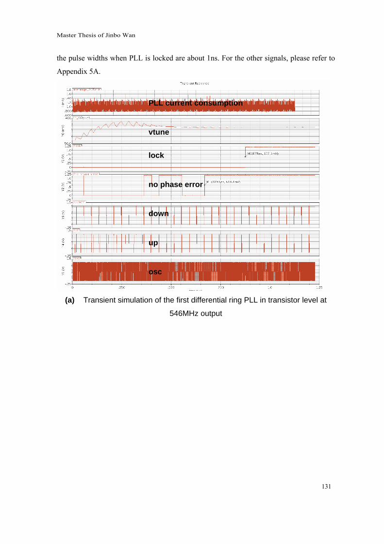
Master Thesis of Jinbo Wan
131
the pulse widths when PLL is locked are about 1ns. For the other signals, please refer to
Appendix 5A.
(a) Transient simulation of the first differential ring PLL in transistor level at
546MHz output
vtune
lock
no phase error
down
up
osc
PLL current consumption

Chapter 6 L-CGU Simulation and Testing
132
(b) Transient simulation of the first differential ring PLL in transistor level at
546MHz output (continued)
vbn
no phase error
fd
ref
down
up

Master Thesis of Jinbo Wan
133
(c) Transient simulation of the first differential ring PLL in transistor level at
546MHz output (zoom in “output” and “osc” to see them clearly)
Figure 6.3 Transient simulation of the first differential ring PLL in transistor level
down
up
osc
out
fd
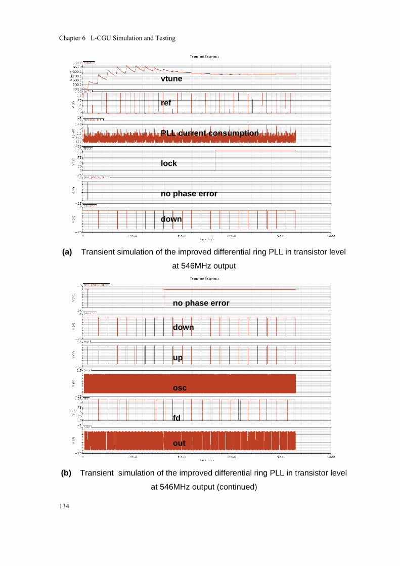
Chapter 6 L-CGU Simulation and Testing
134
(a) Transient simulation of the improved differential ring PLL in transistor level
at 546MHz output
(b) Transient simulation of the improved differential ring PLL in transistor level
at 546MHz output (continued)
vtune
ref
PLL current consumption
lock
no phase error
down
no phase error
down
up
osc
fd
out

Master Thesis of Jinbo Wan
135
(c) Transient simulation of the improved differential ring PLL in transistor level
at 546MHz output (zoom in “output” and “osc” to see them clearly)
Figure 6.4 Transient simulation of the improved differential ring PLL in transistor level at 546MHz output
oscillator output (before buffer)
down
up
osc
out

Chapter 6 L-CGU Simulation and Testing
136
(a) Transient simulation of the LC PLL in transistor level at 546MHz output
(b) Transient simulation of the LC PLL in transistor level at 546MHz output
(continued)
PLL current consumption
lock
no phase error
down
up
ref
down
up
ref
fd
osc
out

Master Thesis of Jinbo Wan
137
(c) Transient simulation of the LC PLL in transistor level at 546MHz output
(zoom in “output” and “osc” to see them clearly)
Figure 6.5 Transient simulation of the LC PLL in transistor level at 546MHz output
The PLLs current consumptions are also shown in Figure 6.3~6.5. For the improved
differential ring PLL, the total current for the PLL at 546MHz is about 735μA. It is
smaller compare to 1mA of the differential ring PLL and 1.7mA of the LC PLL.
6.1.2. PLL Phase Noise and Jitter Simulation
The phase noise and jitter of a PLL can not be easily obtained from SpectreRFTM circuit
simulations. A more convenient approach is to extract phase noise for each PLL building
block, and combine those results to obtain the overall PLL phase noise using a numerical
down
up
ref
fd
osc
out

Chapter 6 L-CGU Simulation and Testing
138
solver like MatLab [6.1]. We have followed this approach.
Figure 6.6, Figure 6.7 and Figure 6.8 show the phase noises of the three developed PLLs.
The blue-line marked “PLL” is the overall phase noise at the PLL output. The green-line
marked “VCO” is the phase noise for the whole VCO in the PLL. The red-line marked
“ref” is the phase noise of the reference crystal oscillator. The light-blue-line is the refer-
ence crystal oscillator phase noise as transferred to the PLL output. The pink-line is the
phase noise of the whole VCO as transferred to the PLL output. The yellow-line is the
phase noise added by the FDIV N. The black-line is the voltage noise at the LF output,
which is the noise contribution mainly due to the noise coupled from the ground through
big capacitors in the LF. The PLL phase noise in figure 6.6~6.8 has a unit of “dB” not
“dBc”. That is because the phase noise we used here is the baseband spectrum ( )S fφ not
the SSB phase noise ( )L f∆ .
Figure 6.6 Phase noise ( )S fφ of the first differential ring PLL at 546MHz output

Master Thesis of Jinbo Wan
139
Figure 6.7 Phase noise ( )S fφ of the improved differential ring PLL at 546MHz output
Figure 6.8 Phase noise ( )S fφ of the LC PLL at 546MHz output
The RMS period jitter of the three developed PLLs is summarized in Table 6.2. These
values have been determined by using the jitter and phase noise relationship as shown in
expression (3.13). The Matlab program to calculate these results is shown in Appendix
6A.

Chapter 6 L-CGU Simulation and Testing
140
Table 6.2 Jitter contributions of each PLL at 546MHz output
VCO part Jitter contribu-
tions
(rms period
jitter)
20 /dB dec−
phase
noise
Noise
floor
Total
Loop
Filter
other
parts
(Ref,
FDIV N,
PFD and
CP)
Total PLL
jitter
Differential
ring PLL 95ps 6.8ps 95.3ps 80.7ps 1.4ps 125ps
Improved
differential ring
PLL
5ps 6.8ps 8.5ps 5.4ps 1.4ps 10ps
LC PLL 8.6ps 6.8ps 11ps 10.7ps 1.4ps 15.4ps
Table 6.2 indicates that the phase noise of the PLL components, except the VCO and LF,
has only a small contribution to the period jitter (see column “other parts”). This relates
to the phase noise part within the PLL loop bandwidth (0-2.6MHz). This reason for this
is because their jitter is suppressed by the LF.
The PLL’s white FM phase noise (-20dB/dec) beyond the loop bandwidth contributes
most to the jitter when VCOK is large. This includes the VCO white FM phase noise and
the LF noise contribution. The jitter will reduce when VCOK is reduced.
Although the noise floor part induced jitter is not so large (6.8ps), it is considered as an
important contribution due to its dependency on the PSN spectrum characteristics. The
PSN spectrum amplitude directly impacts the noise floor, for example a noise floor in-
crease of about 10dB will results in a 30ps jitter contribution instead of 6.8ps. In that case,
the noise floor contribution will dominate the total jitter in the improved differential ring-
oscillator PLL and the LC PLL.

Master Thesis of Jinbo Wan
141
6.1.3. PLL Simulation Conclusion The simulation results for the three PLLs are concluded in Table 6.3. So far it seems that
the improved differential ring-oscillator PLL offers the most advantages for use in an L-
CGU application.
Table 6.3 PLL simulation results
Items Differential ring PLL
Improved differ-ential ring PLL
LC PLL
Operating Frequen-
cies
546MHz, 494MHz, 442MHz, 390MHz, 338MHz, 312MHz,
247MHz, 195MHz, 156MHz, 97.5MHz, 48.75MHz
Jitter at 546MHz 125ps 10ps 15.4ps
Lock time <1µs
Area Occupation 60µm×60µm 90µm×60µm 385µm×325µm
Active Power Con-
sumption
(at 546MHz)
1.2V×1mA 1.2V×735µA 1.2V×1.7mA
L-CGU Supply Volt-
age Nominal digital VDD of 1.2V
Clock gating, clock
enable, and no glitch
during switching
yes
others calibration re-
quired
6.2. PLL Test-Chip Design and Measurement Set-up To validate previous observations for the developed PLLs based on simulation results
from extracted circuit layouts, two PLL test-chips have been designed in TSMC’s 65nm
low-power CMOS technology. This IC technology makes use of 7 metal layers, and the
nominal digital power supply voltage is 1.2V. All three PLLs have been taped-out. The
reason for this is to perform a silicon characterization of the PLL performance than rather

Chapter 6 L-CGU Simulation and Testing
142
relying on the simulation results. At this moment in time, it is not clear of the power
supply noise spectrum used to model the disturbance of the digital block is representative.
Through silicon measurements this model, as well as the noise influence on the PLL
performance will be validated.
The first test-chip contains a digital logic block for noise generation, the differential ring-
oscillator PLL, and the LC PLL. The chip has been taped out in May 2008. At that mo-
ment in time, the improved differential ring-oscillator was not developed yet. Recently, a
second test-chip has been prepared that contains this PLL. The tape-out of this test-chip
is planned in September 2008. In the next subsection we will provide more details about
the content of the first test-chip.
6.2.1. PLL Test-Chip Overview A PLL test-chip has been designed that is composed of, amongst others a digital logic
block, the differential ring-oscillator PLL and the LC PLL. Figure 6.9 shows the layout
of this test-chip design. The test-chip design occupies a silicon area of 2mm×1.5mm,
and has 80 bondpads.
The purpose of the digital logic block is to offer a programmable circuit solution for
generating power supply noise. The digital logic block implements a circular shiftregister
of 8K flip-flops, while using delay lines in between two consecutive flip-flops. On aver-
age, the logic depth of the delay lines is about 20 logic gates. The shiftregister can be
loaded with a data vector for programming the average circuit activity. Its working mode
can be set to generate no circuit activity (clock gated or power down), clock activity only,
or clock activity plus data activity of 0-100%. The circuit activity can be programmed to
be homogeneous, or spatially distributed in particular regions of the shiftregister. In
addition, the digital block is equipped with a linear feedback shift register (LSFR) to
generate random circuit activity which can be inserted at various locations in the shift
register. Finally, the operating frequency of the digital block is programmable, and it is
provided through an I/O pad. It should be clear that such circuit enables a flexible and
programmable solution to generate power supply noise with different magnitudes and
frequency spectrum.

Master Thesis of Jinbo Wan
143
The digital logic block uses four power and ground connections, which are located at the
same position at a different corner of the digital logic block. Such configuration ensures
that a symmetrical noise propagation throughout the logic block. At the top-right corner,
power and ground observation pads have been placed for measuring the power supply
noise spectrum up to a few gigahertz. The digital block is surrounded by power switches
for power gating purposes. Finally, the block is surrounded by power and ground rings.
Figure 6.9 Layout of the first implemented PLL test-chip in 65nm CMOS
The differential ring-oscillator PLL is located in the bottom-right corner of the chip. The
LC PLL is located in the bottom-left corner of the chip. Both PLLs are connected to the
power supply of the digital logic block at the same location, but at a different side of the
digital logic block. The PLLs are equipped with a scan-chain based control register for
setting the proper control signals to the PLLs.

Chapter 6 L-CGU Simulation and Testing
144
Since PLL output frequencies are up to a value of 550MHz, special output buffers are
needed for enabling reliable jitter and phase noise measurements. In this test-chip, five of
those high-frequency outputs make use of the special RF test buffer. The circuit and
layout details of the RF test-buffer will be disclosed in Section 6.2.2.
Finally, the PLL test-chip also contains contributions from other projects, which will not
be described in this thesis.
6.2.2. RF Test Buffer A special output buffer has been designed for providing a reliable off-chip output con-
nection of high-frequency signals. Each PLL has two high-frequency square wave signals
which require such output buffering (see Appendix 5A). The first output signal is “osc”,
which is the test signal of the VCO output. When the PLL is locked, its frequency range
is in between 624MHz and 1092MHz. The second output signal is “output”, which is the
PLL output. When the PLL is locked, its frequency range is in between 48.75MHz and
546MHz. Based on these requirements, the designed RF test buffer allows an input fre-
quency up to 2 GHz and produces at least a -9dBm output. The output impedance of the
RF test buffer is 50Ω, which is easy to match the test cables. For a reliable phase noise
and jitter measurement, the signal power at the input port of the measurement equipment
should not be lower than -16dBm. It is important to mention that a DC blocking capacitor
(such as 1000pF) is required in between the RF test buffer output and the measurement
equipment. This capacitor is used for blocking the DC bias voltage of the RF test buffer ,
and it should be located close to the chip output pin on the application printed-circuit
board
Figure 6.10 shows the circuit schematic of the proposed RF test buffer. One RF test
buffer consumes about 10mA of current. This large current made us to choose a differen-
tial structure, because it can reduce the current injected into the substrate. The required
differential inputs are produced by the same design in the PFD. In order to ensure that the
PLL output phase noise and jitter is not polluted by the RF test buffer, the buffer has
been supplied from a dedicated but clean analog power supply and ground. Figure 6.11
shows the layout of the RF test buffer. It occupies 0.005 mm2 of silicon area.

Master Thesis of Jinbo Wan
145
Figure 6.10 Circuit schematic of the RF test buffer
Figure 6.11 Layout of the RF test buffer
6.3. Summary The simulation results for the three PLLs which were designed in Chapter 5 are shown
and discussed. Based on the results, the improved differential ring PLL has found to be

Chapter 6 L-CGU Simulation and Testing
146
the lowest jitter, smallest power consumption and acceptable in area. It is the best candi-
date for the L-CGU applications. The test structure and some supplements such as test
RF buffer are also introduced in this chapter.
Appendix 6A Matlab Program for the PLL Phase Noise and Jitter Calculations
The phase noise and jitter calculation programs for three PLLs are the same except for
the PLL loop parameters and phase noise simulation values. So here only the program
for the differential ring PLL is shown below.
clear; K_vco = 3e9*2*pi/2; % Be careful of the unit f_osc = 26e6; f_vco = 1092e6/2; % f_exp = [6.3:0.01:9]; f = 10.^f_exp; s = i*2*pi*f; % Be careful of the unit N = f_vco/f_osc; % K =2*pi*f_osc/10; % K = K_det*K_vco*K1/N; % Be careful of the unit b = 9; % b = 1 + C/C3; % b = 9 is wanted tal_2 = sqrt(b)/K;%*2*pi); % tal_2 = R2*C; K_nomal = K*tal_2;%*2*pi; % K_normal = 3 is wanted pole_3 = b/tal_2; zero_1 = 1/tal_2; damp_app = sqrt(K_nomal/4); % Aprroximate damping factor. When the third pole is far away, the third order pll is aproximate second order pll within loop band width. wn_app = K/(2*damp_app); % Aprroximate natural freq % Charge pump filter R1 = 51.6e3 C1 = tal_2/R1 C2 = C1/(b-1) % PFD ip = K*2*pi*N*b/(K_vco*R1*(b-1)) K_det = ip/(2*pi); % Z_f = (b-1)*(s*tal_2+1)./(b*s*C1.*(s*tal_2/b+1)); G_f = K_det*K_vco*Z_f./s; H_f = G_f*N./(N+G_f);

Master Thesis of Jinbo Wan
147
E_f = N./(N+G_f); figure(1); semilogx(f,20*log10(abs(H_f))); grid on; title('PLL System Transfer Function H(f)'); xlabel('frequency'); ylabel('dB'); figure(2); semilogx(f,20*log10(abs(E_f))); grid on; title('PLL Error Transfer Function E(f)'); xlabel('frequency'); ylabel('dB'); %%%%%%%%%%%%%%% t = [6.0:3*0.1/f_osc:3*10/f_osc]; delta_w = 100e3*2*pi; phase_error_t = delta_w/wn_app*(sin(sqrt(1-damp_app^2)*wn_app.*t)/sqrt(1-damp_app^2)).*exp(-damp_app*wn_app*t); figure(3); plot(t, phase_error_t); grid on; title('Transient Phase Error'); xlabel('second'); ylabel('rad'); % Phase nosie of VCO (without power supply noise) after divide-by-2 at 546MHz S0_VCO = -120; % Noise floor in dB !! S2_VCO = -51.16 -6+3; % White FM part in dB !! f2_VCO = 1e6; % The offset frequency point to get S2_VCO S3_VCO = -56.69 -6+3; % Flicker FM part in dB !! f3_VCO = 1e5; % The offset frequency point to get S3_VCO Sf_VCO = (10^((S3_VCO+30*log10(f3_VCO))/10)./f.^3 + 10^((S2_VCO+20*log10(f2_VCO))/10)./f.^2 + 10^(S0_VCO/10)); % Phase nosie of ref OSC S0_OSC = -150; % Noise floor in dB !! S2_OSC = -140 +3; % White FM part in dB !! f2_OSC = 1e3; % The offset frequency point to get S2_OSC S3_OSC = -80 +3; % Flicker FM part in dB !! f3_OSC = 10; % The offset frequency point to get S3_OSC Sf_OSC = (10^((S3_OSC+30*log10(f3_OSC))/10)./f.^3 + 10^((S2_OSC+20*log10(f2_OSC))/10)./f.^2 + 10^(S0_OSC/10)); % Phase noise of frequency divider S0_FD = -110.1; % White noise in dB S1_FD = -107; % Flicker noise in dB f1_FD = 1e3; % The offset frequency point to get S1_FD Sf_FD = 10^((S1_FD+10*log10(f1_FD))/10)./f + 10^(S0_FD/10);

Chapter 6 L-CGU Simulation and Testing
148
% voltage noise of PFD, CP and filter at the filter output V0_filter = -119.1; % White noise in dB V1_filter = -107; % Flicker noise in dB f1_filter = 1e3; % The offset frequency point to get V1_filter V_filter = 10^((V1_filter+10*log10(f1_filter))/10)./f + 10^(V0_filter/10); % PLL Phase nosie Sf_pll =(Sf_OSC + Sf_FD + V_filter./(abs(Z_f*K_det).^2)).*abs(H_f).^2 + Sf_VCO.*abs(E_f).^2; Sf_pll_dB = 10*log10(Sf_pll); figure(4); semilogx(f, Sf_pll_dB, '.', f, 10*log10(Sf_VCO),'--', f, 10*log10(Sf_OSC), '*', f, 10*log10(Sf_OSC.*abs(H_f).^2), f, 10*log10(Sf_VCO.*abs(E_f).^2),':', f, 10*log10(Sf_FD), f, 10*log10(V_filter),'+'); grid on; ylim([6.-160 -50]); title('PLL Phase Noise'); xlabel('offset frequency'); ylabel('dB'); legend('PLL','VCO phase noise', 'ref', 'ref * H(f)', 'VCO * E(f)',' FDIV N phase noise', 'voltage noise of the LF output'); %%%%%%%%%Jitter Z_fun =@(freq) (b-1)*(i*2*pi*freq*tal_2+1)./(b*i*2*pi*freq*C1.*(i*2*pi*freq*tal_2/b+1)); G_fun =@(freq) K_det*K_vco*Z_fun(freq)./(i*2*pi*freq); H_fun =@(freq) G_fun(freq)*N./(N+G_fun(freq)); E_fun =@(freq) N./(N+G_fun(freq)); Sf_VCO_fun =@(freq) (10^((S3_VCO+30*log10(f3_VCO))/10)./freq.^3 + 10^((S2_VCO+20*log10(f2_VCO))/10)./freq.^2 + 10^(S0_VCO/10)); Sf_OSC_fun =@(freq) (10^((S3_OSC+30*log10(f3_OSC))/10)./freq.^3 + 10^((S2_OSC+20*log10(f2_OSC))/10)./freq.^2 + 10^(S0_OSC/10)); Sf_FD_fun =@(freq) 10^((S1_FD+10*log10(f1_FD))/10)./freq + 10^(S0_FD/10); V_filter_fun =@(freq) 10^((V1_filter+10*log10(f1_filter))/10)./freq + 10^(V0_filter/10); int_fun_VCO_white_FM_part = @(freq) 10^((S2_VCO+20*log10(f2_VCO))/10)./freq.^2.*abs(E_fun(freq)).^2.*(sin(pi*freq/f_vco)).^2/(pi*f_vco)^2; int_fun_VCO_noise_floor_part = @(freq) 10^(S0_VCO/10).*abs(E_fun(freq)).^2.*(sin(pi*freq/f_vco)).^2/(pi*f_vco)^2; int_fun_VCO_part_total = @(freq) Sf_VCO_fun(freq).*abs(E_fun(freq)).^2.*(sin(pi*freq/f_vco)).^2/(pi*f_vco)^2; int_fun_LF_part = @(freq) (V_filter_fun(freq)./(abs(Z_fun(freq)*K_det).^2)).*abs(H_fun(freq)).^2.*(sin(pi*freq/f_vco)).^2/(pi*f_vco)^2;

Master Thesis of Jinbo Wan
149
int_fun_other_pll_part = @(freq) (Sf_OSC_fun(freq) + Sf_FD_fun(freq)).*abs(H_fun(freq)).^2.*(sin(pi*freq/f_vco)).^2/(pi*f_vco)^2; int_fun_total_jitter_PLL = @(freq) int_fun_VCO_part_total(freq) + int_fun_LF_part(freq) + int_fun_other_pll_part(freq); Jc_VCO_white_FM_part = sqrt(quad(int_fun_VCO_white_FM_part,1E3, f_vco/2)) Jc_fun_VCO_noise_floor_part = sqrt(quad(int_fun_VCO_noise_floor_part,1E3, f_vco/2)) Jc_VCO_part_total = sqrt(quad(int_fun_VCO_part_total,1E3, f_vco/2)) Jc_LF_part = sqrt(quad(int_fun_LF_part,1E3, f_vco/2)) Jc_other_pll_part = sqrt(quad(int_fun_other_pll_part,1E3, f_vco/2)) Jc_total = sqrt(quad(int_fun_total_jitter_PLL,1E3, f_vco/2))
Reference [6.1] K. Kundert, “Predicting the Phase Noise and Jitter of PLL-Based Frequency
Synthesizers,” Available from www.designers-guide.org/Analysis.

Future Work
150
7. Conclusions In this work we have investigated suitable local clock generator units (L-CGU) for use in
multiple-power domain system chips. Local clocking is attractive for advanced power
management applications for replacing the traditional central clocking. The most impor-
tant requirement of the L-CGU is that it should generate a robust high-quality, low-jitter
clock (period jitter <30ps), while operating from the digital ‘noisy’ power supply. The L-
CGU output frequency should be from 550MHz down to 50MHz with steps of 50MHz.
Phase noise and jitter under noisy power supply conditions has been analyzed. A power
supply noise model has been developed that enabled us to explore trade-offs involved
between different oscillators approaches.
A number of oscillator types have been compared on various defined quality metrics.
Two suitable candidates for use in an L-CGU have been identified. The first solution is a
differential ring-oscillator based VCO, and the second one is a complementary differen-
tial LC oscillator. Both oscillator types have been implemented in a PLL in 65nm LP-
CMOS.
A L-CGU has been implemented by an integer-N PLL. Three different versions have
been developed. The first version is based on a differential ring-oscillator VCO, the
second version based on an improved differential ring-oscillator VCO, and the third one
is based on the differential LC oscillator. Post-layout extracted simulations showed that
the improved differential ring-oscillator PLL achieves the best jitter performance, lowest
power consumption, and small area occupation. However, it requires an initial calibration
before use. It is considered as the preferred solution for implementation of an L-CGU.
Table 7.1 summarizes the key design characteristics of the different implementations.

Master Thesis of Jinbo Wan
151
Table 7.1 L-CGU Design Characteristics in 65nm LP-CMOS
RMS period
jitter
Active current Circuit Area Specialties
Differential ring
PLL
125ps 1mA 60×60µm2 no
Improved differen-
tial ring PLL
10ps 735µA 90×60µm2 initial calibration
LC PLL 15.4ps 1.7mA 300×
400µm2
no
Furthermore, we have analyzed the jitter performance of clock net buffers under power
supply noise conditions. In general, we found that the jitter in digital circuits can be
dominated by the jitter contributed by the clock buffers in the clock distribution network.
In that case, the efforts to develop a high-quality low-jitter L-CGU would have no mean-
ing.

Future Work
152
Future Work Although we have developed a suitable L-CGU solution, more work is needed to find
answers to some questions that could not be addressed in the timeframe of this investiga-
tion.
First, the power supply noise model that has been developed in this work needs to be
validated and calibrated through silicon measurements. This is possible when the imple-
mented test-chip design will return from fabrication and assembly.
Second, silicon measurements of the developed L-CGUs are required to confirm our
observations in this investigation. Noise correlations should be studied as well as the
means how to reduce the noise floor of the buffers.
Third, an investigation should be started on the jitter performance of the clock distribu-
tion network. The clock distribution could be responsible for most of the jitter experi-
enced in digital circuits. The optimization for achieving a low-jitter and low clock skew
clock delivery is recognized as a very challenging task.