design of a 3d integrated circuit for manipulating and sensing
TRANSCRIPT

DESIGN OF A 3D INTEGRATED CIRCUIT FOR MANIPULATING AND SENSING BIOLOGICAL NANOPARTICLES
by
Samuel J. Dickerson
B.S. in Computer Engineering, University of Pittsburgh, 2003
Submitted to the Graduate Faculty of
the School of Engineering in partial fulfillment
of the requirements for the degree of
Master of Science
University of Pittsburgh
2007

ii
UNIVERSITY OF PITTSBURGH
SCHOOL OF ENGINEERING
This thesis was presented
by
Samuel J. Dickerson
It was defended on
April 13, 2007
and approved by
Steven P. Levitan, Professor, Electrical and Computer Engineering (Thesis Co-Advisor)
Donald M. Chiarulli, Professor, Computer Science (Thesis Co-Advisor)
William Stanchina, Chairman and Professor, Electrical and Computer Engineering
Kevin P. Chen, Assistant Professor, Electrical and Computer Engineering

iii
Copyright © by Samuel J. Dickerson
2007

DESIGN OF A 3D INTEGRATED CIRCUIT FOR MANIPULATING AND SENSING BIOLOGICAL NANOPARTICLES
Samuel J. Dickerson, M.S.
University of Pittsburgh, 2007
We present the design of a mixed-technology microsystem for electronically manipulating and
optically detecting nanometer scale particles in a fluid. This lab-on-a-chip is designed using 3D
integrated circuit technology. By taking advantage of processing features inherent to 3D chip-
stacking technology, we create very dense dielectrophoresis electrode arrays. During the 3D
fabrication process, the top-most chip tier is assembled upside down and the substrate material is
removed. This puts the polysilicon layer, which is used to create geometries with the process’
minimum feature size, in close proximity to a fluid channel etched into the top of the stack. This
technique allows us to create electrode arrays that have a gap spacing of 270 nm in a 0.18 µm
SOI technology. Using 3D CMOS technology also provides the additional benefit of being able
to densely integrate analog and digital control circuitry for the electrodes by using the additional
levels of the chip stack.
For sensing particles that are manipulated by dielectrophoresis, we present a method by
which randomly distributed nanometer scale particles can be arranged into periodic striped
patterns, creating an effective diffraction grating. The efficiency of this grating can be used to
perform a label-free optical analysis of the particles.
The functionality of the 3D lab-on-a-chip is verified with simulations of Kaposi’s
sarcoma-associated herpes virus particles, which have a radius of approximately 125 nm, being
manipulated by dielectrophoresis and detected optically.
iv

TABLE OF CONTENTS
ABSTRACT................................................................................................................................. IV
PREFACE..................................................................................................................................... X
1.0 INTRODUCTION........................................................................................................ 1
1.1 PROBLEM STATEMENT................................................................................. 5
1.2 STATEMENT OF WORK.................................................................................. 6
1.3 KEY CONTRIBUTIONS.................................................................................... 7
1.4 THESIS ROAD MAP.......................................................................................... 8
2.0 THEORY OF DIELECTROPHORESIS................................................................... 9
2.1 FORCES EXERTED ON NANOSCALE PARTICLES................................ 13
2.1.1 Hydrodynamic forces.................................................................................. 14
2.1.2 Electro-thermal forces ................................................................................ 15
2.1.3 Random Brownian force ............................................................................ 15
3.0 3D LAB-ON-A-CHIP FOR DIELECTROPHORESIS .......................................... 17
3.1 FABRICATION OF 3D INTEGRATED CIRCUITS .................................... 17
3.2 DESIGN OF 3D LAB-ON-A-CHIP ................................................................. 19
3.2.1 Design of Dielectrophoresis Electrodes..................................................... 19
3.2.2 Design of Analog Electronics ..................................................................... 21
3.2.3 Design of Digital Electronics ...................................................................... 22
v

4.0 OPTICAL DETECTION OF TRAPPED PARTICLES ........................................ 25
4.1 DIFFRACTION GRATING THEORY........................................................... 26
4.2 SENSING PARTICLES USING DIFFRACTIVE OPTICS.......................... 27
5.0 SIMULATION STUDY OF 3D LAB-ON-A-CHIP ................................................ 30
5.1 SIMULATIONS OF THE ELECTRONICS................................................... 31
5.2 FINITE ELEMENT ANALYSIS OF DIELECTORPHORESIS FIELDS .. 34
5.3 FINITE ELEMENT ANALYSIS OF TEMPERATURE GRADIENTS...... 38
5.4 CALCULATION OF FLUID VELOCITY PROFILE .................................. 39
5.5 VIRTUAL-WORK CALCULATION OF ELECTRICAL FORCES .......... 41
5.5.1 Electrical Modeling of KSHV Particles .................................................... 41
5.5.2 Virtual Work Calculation of Dielectrophoretic Force Vector................ 42
5.6 DISCRETE-TIME SIMULATION OF PARTICLE MOTION ................... 43
5.7 RIGOROUS COUPLED WAVE ANALYSIS OF GRATINGS ................... 47
5.7.1 2D Diffractive Analysis............................................................................... 48
5.7.2 3D Diffractive Analysis............................................................................... 51
6.0 POST-FABRICATION PROCEDURES FOR 3D LAB-ON-A-CHIP ................. 54
6.1 TEST PLAN ....................................................................................................... 55
7.0 SUMMARY ................................................................................................................ 58
7.1 CONCLUSIONS................................................................................................ 59
7.2 FUTURE WORK............................................................................................... 60
APPENDIX A. 3D INTEGRATED CIRCUIT PROCESS DESIGN LAYERS..................... 62
APPENDIX B. 3D LAB-ON-A-CHIP PINOUT........................................................................ 63
BIBLIOGRAPHY....................................................................................................................... 65
vi

LIST OF TABLES
Table 5.1. Average power consumption of 3D lab-on-a-chip ...................................................... 33
Table 7.1. Summary of 3D lab-on-a-chip specifications .............................................................. 58
Table B.1. 3D lab-on-a-chip pin names and descriptions..............................................................64
vii

LIST OF FIGURES
Figure 1.1. Goal of lab-on-a-chip devices ...................................................................................... 1
Figure 1.2. Image of one KSHV virion............................................................................................3
Figure 1.3. Biological scaling versus integrated circuit technology scaling....................................4
Figure 1.4. 3D lab-on-a-chip............................................................................................................5
Figure 2.1. Electrically neutral particle in a non-uniform electric field ..........................................9
Figure 2.2. Example dielectrophoretic spectrum ...........................................................................12
Figure 2.3. Forces exerted on a particle moving in fluid ...............................................................13
Figure 3.1. Fabrication procedures for MIT 3D integrated circuit process ...................................18
Figure 3.2. Organization of 3D lab-on-a-chip ...............................................................................19
Figure 3.3. Cross-sectional view of 3D lab-on-a-chip...................................................................20
Figure 3.4. Analog multiplexer circuit...........................................................................................22
Figure 3.5. Block diagram of digital circuits .................................................................................22
Figure 3.6. VLSI layout of lab-on-a-chip ......................................................................................23
Figure 4.1. Diffraction grating .......................................................................................................26
Figure 4.2. Particles arranged into diffraction grating...................................................................29
Figure 5.1. Simulation flow used to model 3D lab-on-a-chip .......................................................31
Figure 5.2. Waveforms of four 4:1 analog multiplexers................................................................32
Figure 5.3. Frequency response of electrodes................................................................................33
viii

Figure 5.4. Electric field with single maximum ............................................................................34
Figure 5.5. Profile of single-maximum electric field.....................................................................35
Figure 5.6. Alternating electric field minima and maxima............................................................36
Figure 5.7. Negative dielectrophoresis trapping ............................................................................37
Figure 5.8. Temperature variations due to joule heating................................................................39
Figure 5.9. Direction of electro-thermal force vector ....................................................................40
Figure 5.10. KSHV virion electrical model ...................................................................................42
Figure 5.11. 3D model used to calculate dielectrophoretic force vector .......................................43
Figure 5.12. Motion simulation of particles...................................................................................45
Figure 5.13. Multi-layered grating model......................................................................................47
Figure 5.14. Reflected diffraction efficiency versus diffraction order ..........................................49
Figure 5.15. Reflected diffraction efficiency versus cross-sectional area of particles ..................50
Figure 5.16. Depiction of the differences in the nanoparticle grating based on concentrations....51
Figure 5.17. Diffraction efficiency versus diffraction order for 3D grating model .......................52
Figure 6.1. Setup for measuring diffraction efficiency of gratings................................................56
Figure A.1. Cross-section of design layers in lincoln labs 0.18 µm process .................................62
Figure B.1. Pinout of 3D lab-on-a-chip .........................................................................................63
ix

PREFACE
I would first like to thank my advisors, Dr. Steven Levitan and Dr. Donald Chiarulli. Most
graduate students get one advisor throughout their academic career, but I’ve been fortunate to
have two great ones. Special thanks to Steve for taking me into his research group and to Don
for making sure I never have a dull moment.
I would also like to thank Sandy, Joni, Theresa, Bill and Jim for all the assistance they’ve
given me in my day-to-day activities, without whom the third floor of Benedum hall would be in
chaos.
I especially would like to thank all of the many other students with whom I’ve had the
pleasure to work with throughout the years, Bryan, Jose, Mike, Majd, Arnaldo, Joel and Ben.
Each of them are unique folks whom, as much as I try to, I will never forget. A special thanks to
Jason for selflessly giving of himself to me and others with whatever oddball task we bother him
with.
I would like to thank Aunt Carolyn and Papa for their support. Thanks to Aunt Joan for
her parking space and suggestion to “go to college”. I would like to thank Isaac for giving me an
early start on my way to geekiness with his comic book movies and video games, making me fit
in with the other engineers. Thanks to mom and dad for being the best parents ever, and keeping
me supplied with vitamins to keep my brain going.
x

Finally, I would like to thank the most important person to me, a person so important that
not only do they get their own paragraph in my thesis; but their own page, my wonderful wife
Naomi. Without her I would probably starve, stink, and wear wrinkled clothes (more often) and
just wouldn’t enjoy things as much, you truly are the best wife.
-Sam
xi

1.0 INTRODUCTION
In this thesis, we present the design of a lab-on-a-chip that can manipulate biological particles
that are on the same size scale as viruses and propose a new method for sensing them. Lab-on-a-
chip devices are an emerging microsystem technology for which the goal is to integrate multiple
laboratory functions on to a single chip (figure 1.1). These chips are primarily used to assay
biological particles. They can perform functions such as sample preparation, microfluidic
transport, synthesis, analysis and detection.
Figure 1.1 Illustration of the goal of lab-on-a-chip microsystems, to integrate multiple laboratory functions onto a single chip [44],[45].
There are many advantages that come from the miniaturization of biological laboratory
functions [46]. For example, it reduces sample size requirements, as only nano-liter or pico-liter
1

volumes are needed to carry out an analysis. Lab-on-a-chip microsystems are capable of
performing high-throughput analyses, reducing the required processing time from hours to a
matter of seconds. These devices allow for experimentation to be done with superior resolution,
allowing for isolation and manipulation of single biological particles such as cells and viruses.
Furthermore, lab-on-a-chip microsystems are cost-efficient because electronics can be integrated
onto them and they are fabricated using processes in which they can be mass-produced. All of
these factors make the future of lab-on-a-chip microsystems bright. One recent market analysis
reports that applications of microfluidics to the life sciences have a global market that could rise
to around 1.9 billion U.S. dollars by 2010[47]. In addition, the availability of devices that can
automatically perform rapid diagnostics in a compact, inexpensive package is going to be
particularly beneficial to countries in the developing world that lack the infrastructure to support
modern medical technologies [44].
Dielectrophoresis is used in a broad range of lab-on-a-chip applications such as
cytometry, cell sorting, and mixture separation. It is the physical phenomena where electric fields
are used to control the movement of particles that are in a fluid. The technique has been shown
to be a viable method for manipulating small particles without the need for contact [1,2,3] and it
is the method used by the lab-on-a-chip presented in this thesis. Current dielectrophoresis-based
lab-on-a-chip implementations have primarily focused on the manipulation of cells and have
already been found to be promising for furthering cancer research [4,5,6,7]. Part of our research
goals is to apply these techniques to smaller particles, such as viruses and macromolecules.
Kaposi’s sarcoma-associated herpes virus (KSHV) is a recently discovered DNA virus
that causes disease in humans [8]. KSHV is one of the most interesting subjects in molecular
virology because it is one of the few examples of a virus that can cause cancerous tumors. The
2

study of KSHV allows researchers to form a link between the structure of tumor viruses and
modern cancer biology [9]. KSHV is a spherical virion that has a radius of approximately 125
nm (figure 1.2). KSHV’s extremely small size creates the need for instrumentation that will
allow it to be efficiently manipulated and analyzed. We use KSHV as a model for the kinds of
biological particles we would like to manipulate and detect with our lab-on-a-chip design.
Figure 1.2. Image of one KSHV virion [10]
One trend of microelectronics research is similar to that of biomedical research in that
both technologies are scaling downwards in size (figure 1.3). However, current technology
limitations restrict most lab-on-a-chip devices to fabricating dielectrophoresis electrodes that are
not well-suited for the manipulation of biological nanoparticles, such as viruses. Figure 1.3
shows a depiction of a typical integrated circuit. Integrated circuits are fabricated by using
photolithography to pattern multiple layers that are used to create active devices and
interconnect. The topmost layer patterned on an integrated circuit, used for external I/O, can
only be fabricated at micron-scale dimensions and is the design layer that is most commonly
used to create lab-on-a-chip electrodes. Even for advanced technologies, the design layers that
are used to create geometries with nano-scale feature sizes are located towards the bottom of a
chip and are surrounded by a thick substrate layer, making them inaccessible for use as
electrodes. These restrictions make it a challenge to implement a system that can efficiently
manipulate nanometer scale biological particles using conventional integrated circuit technology.
3

Figure 1.3. Illustration of biological scaling versus integrated circuit technology scaling [38]
Another challenge facing the development of lab-on-a-chip devices is the development of
detection mechanisms that are inexpensive and non-invasive. Microscopy techniques are non-
invasive but, they are costly and not suitable for use in a mobile device. The technique of
labeling particles (fluorescence, magnetic, etc.) is a low-cost detection solution but, it often
requires that the analyte be modified in some unnatural way and is also not well-suited for use
outside of a laboratory setting.
Overcoming these two challenges gives the motivation for this work: The design of a
dielectrophoresis-based lab-on-a-chip that can efficiently manipulate and detect nanometer scale
particles (figure 1.4). The lab-on-a-chip is designed using 3D integrated circuit technology, in
4

which chips are stacked vertically. We take advantage of fabrication features found in this
technology to create a high-density electrode array for dielectrophoresis. In addition to
manipulating nanometer scale biological particles, we also present a new label-free optical
detection scheme for sensing particles on lab-on-a-chip microsystems.
Figure 1.4. 3D lab-on-a-chip presented in this work. Inset shows a close-up view of its high-density electrode array.
1.1 PROBLEM STATEMENT
The research questions we address in this thesis are: What is the best way to design a lab-on-a-
chip that can efficiently manipulate virus-sized particles? How can information about nanometer
scale particles being manipulated by the lab-on-a-chip be analyzed in a practical way? And
finally, how can the behavior of a lab-on-a-chip microsystem that operates in many physical
domains be accurately modeled?
5

1.2 STATEMENT OF WORK
In order to answer the aforementioned questions, we performed the following tasks:
• Design of 3D lab-on-a-chip: We designed a dielectrophoresis-based lab-on-a-chip using
3D integrated circuit technology. The design includes an electrode array for
dielectrophoresis, microfluidic trenches, digital circuits and analog electronics. The
GDSII layout of the design was submitted to be fabricated in MIT Lincoln Labs 0.18 µm
SOI 3D process.
• Development of technique for detection of nanometer scale particles: We developed
a novel scheme for detecting biological particles on lab-on-a-chip microsystems. We
show how very small particles can be manipulated such that they can be detected using
conventional diffractive optics.
• Modeling of 3D lab-on-a-chip: We verified the functionality of the lab-on-a-chip by
performing a simulation study of it manipulating Kaposi’s sarcoma-associated herpes
virus particles. This task includes the use of multiple CAD tools to characterize the
behavior of our system in the electronic, electrostatic, optical, thermodynamic,
microfluidic and mechanical domains. We also wrote a custom discrete-time simulator
that uses these simulation results to model the movement of the particles within the
microfluidic trench.
6

1.3 KEY CONTRIBUTIONS
From the results of our work, we make the following research contributions:
• Novel lab-on-a-chip design: This is the first lab-on-a-chip to be implemented using 3D
integrated circuit technology. In the design, we introduce innovative concepts for
creating on-chip electrode arrays and microfluidic channels. Our design also
demonstrates the advantages that 3D integration provides in terms of adding robust
functionality to lab-on-a-chip devices.
• New technique for detection of nanometer scale particles: We provide a new, cost-
effective solution to sensing extremely small particles on lab-on-a-chip microsystems.
Our technique avoids the use of expensive equipment to collect information about
particles that are below the diffraction limit of optical microscopes. The technique we
devised is especially well suited for biological particles.
• Methodology for simulating lab-on-a-chip microsystems: We show how a lab-on-a-
chip microsystem that simultaneously interacts in many domains can be accurately
modeled by using various CAD tools for each of those domains and then integrating the
results with the use of a custom tool.
7

1.4 THESIS ROAD MAP
The rest of this thesis organized as follows: Chapter 2 gives a theoretical background of
dielectrophoresis and discusses some of the issues that arise when dielectrophoresis is used to
control nanometer scale particles. Detailed descriptions of the lab-on-a-chip architecture and
fabrication procedures are provided in chapter 3. Chapter 4 shows the technique we developed to
sense particle samples on lab-on-a-chip microsystems with diffractive optics. Chapter 5 presents
the results from a simulation study of the lab-on-a-chip manipulating and detecting KSHV
particles. Post-fabrication procedures and a test plan for the initial prototypes are given in
chapter 6. Finally, we present a summary of our work and conclusions in Chapter 7, followed by
a discussion of possible future directions.
8

2.0 THEORY OF DIELECTROPHORESIS
In this chapter, we provide an overview of the theory behind the central mechanism we use to
manipulate particles, dielectrophoresis (DEP). Dielectrophoresis is the physical phenomenon
whereby a particle with no net charge undergoes motion in response to a spatially non-uniform
electric field [11]. When an electrically neutral particle is placed in the presence of a set of
electrodes configured to create a non-uniform electric field, the particle becomes polarized. As a
result of this polarization (figure 2.1), the negative charges are separated by a small distance
from the positive charges and because the particle is neutral, the two charges on the body are
opposite but equal in magnitude.
Figure 2.1 Electrically neutral particle in the presence of a spatially non-uniform electric-field. The dipole moment induced within the particle results in a translational force.
9

In order to derive the translational force that causes the particle to move, the polarized
body can be modeled as a small physical dipole [12]. The force on an infinitesimal dipole is
EpF effdipole
rrr∇⋅= (2.1)
Equation (2.1) shows that there is no net force on a dipole unless the externally imposed electric
field is nonuniform. In the case of a sphere suspended in a dielectric medium (for
dielectrophoresis, the medium is typically an aqueous solution), the effective dipole moment
induced by the electric field Er
is defined as
E2
r4p *m
*p
*m
*p
m3
peff
rr⎟⎟⎠
⎞⎜⎜⎝
⎛
+
−=
εεεε
επ (2.2)
where rp is the radius of the particle, εm is the permittivity of the medium and , represents
the complex permittivities of the particle and medium respectivly. Complex permittivity is a
function of an objects conductivity σ and is given by
*pε
*mε
ωσεε j* −= (2.3)
at an angular frequency of ω. From equations (2.1) and (2.2) the expression for the time
averaged force exerted on the particle in an AC field is:
[ ] 2RMSCM
3pmDEP EKr2F ∇= Reπε
r (2.4)
where
**
**
mp
mpCM 2K
εεεε
+
−= (2.5)
The term KCM is known as the Clausius-Mossotti factor [12] and is a measure of relative
permittivities between the particle and the surrounding medium. It can be seen from equations
(2.4) and (2.5) that this factor determines the direction of the dielectrophoretic force. When the
10

sign of Re[Kcm] is positive, the particle is more polarizable than its surrounding medium and it
undergoes what is known as positive dielectrophoresis (pDEP). While undergoing positive
dielectrophoresis, the force vector is directed along the gradient of electric field intensity .
Under these conditions, the particles are attracted to the locations of electric field intensity
maxima and repelled from the minima. The opposite occurs when Re[K
2RMSE∇
cm] is negative, referred
to as negative dielectrophoresis (nDEP).
Dielectrophoresis techniques work for both AC and DC excitations of the electric field.
By substituting equation (2.3) into (2.5), the high and low frequency limits for Re[Kcm] are found
to be
[ ]mp
mpCM0 2
Kσσσσ
ω +
−=
→Relim (2.6)
[ ]mp
mpCM 2
Kεεεε
ω +−
=∞→
Relim (2.7)
Equations (2.6) and (2.7) show that the relative difference in ohmic losses dominates the low
frequency behavior of , while dielectric polarization effects are more significant at high
frequencies. These equations also show that Re[K
DEPFr
cm] is bounded (-½ < Re[Kcm] < 1) regardless
of frequency. Figure 2.2 shows an example dielectrophoretic spectrum with σp < σm and εp > εm.
For this case, the particles would move under the influence of nDEP forces at low frequencies
and pDEP forces at all frequencies above the zero-crossing of Re[Kcm].
11

Figure 2.2 Example dielectrophoretic spectrum with σp < σm and εp > εm
In summary, from equations (2.4)-(2.7) we observe the following main features of
dielectrophoresis:
• is present only when the electric field is spatially nonuniform. DEPFr
• can be observed with AC as well as DC excitations of the electric field. DEPFr
• is not affected by the polarity of DEPFr
Er
. It depends only on Er
or RMSEr
• is directly proportional to the volume of the particle. DEPFr
• direction depends on the relative permittivities, as indicated by KDEPFr
cm
o pDEP forces (Re[Kcm] > 0) cause particles to move towards the regions with
the strongest electric field strength.
o nDEP forces (Re[Kcm] < 0) cause particles to move towards the regions with
the weakest electric field strength.
12

2.1 FORCES EXERTED ON NANOSCALE PARTICLES
Particles actuated by dielectrophoresis move in a fluidic medium, therefore other forces have to
be taken into consideration when describing their motion (figure 2.3). The most considerable of
which are the hydrodynamic forces. The velocity of the particles will be significantly slowed by
the resistance of drag forces while buoyancy forces may cause them to naturally float. In
addition to these, under certain conditions forces that have been considered insignificant when
manipulating micron scale particles (e.g. cells) can become more pronounced at the nanometer
scale (e.g. viruses). This includes both electro-thermal effects that induce additional drag and
random Brownian forces. These effects have been observed experimentally [13,14,15]. If the
dielectrophoretic force is not strong enough, these forces will cause the particles to move at
unreasonably slow speeds, move to unintended locations or, possibly, not move at all.
In this section, we provide a brief review of these forces as they relate to
dielectrophoresis. Full derivations are not provided and other references are suggested. See
references [14,16,17] for a more complete treatment.
Figure 2.3 Forces exerted on a particle moving in fluid, under the influence of dielectrophoresis
13

2.1.1 Hydrodynamic forces
In fluid mechanics, the Reynolds number is the ratio used to measure the relative importance of
inertial forces to viscous forces and is defined as [18]
m
mmLReηνρ
= (2.8)
where ρm is the fluid density, νm is the mean fluid velocity, L is the characteristic length of the
system and ηm is the dynamic fluid viscosity. Nanometer scale particles have very small
Reynolds numbers; therefore they experience laminar Stokes flows in which inertia is negligible
[18].
The motion of fluids is described by a set of partial differential equations known as the
Navier-Stokes equations. For the case of a small Reynolds number sphere undergoing laminar
flow in an incompressible, Newtonian fluid, these equations reduce to a simple closed form [18].
Since we are manipulating nanometer scale biological particles in an aqueous medium that meets
the previously mentioned criteria (e.g. water or a KCL buffer solution) we can model the drag
force exerted on the moving particles using Stoke’s law:
( )pmpmdrag r6F ννπη −= (2.9)
where νp is the velocity of the particle. Stokes’s law has been experimentally verified to be an
accurate estimate of the drag force when Re< 0.5 and deviates by only about 10% at Re = 1 [19].
The other hydrodynamic force exerted on particles manipulated by dielectrophoresis is
buoyancy [16]
( )gVF mppbuoy ρρ −= (2.10)
where g is the acceleration due to gravity and the ρp and Vp represent the density and volume of
the particle. Since the volume of a nano-particle is small, the magnitude of the buoyancy force is
14

also small. However, the densities may be such that DEPFr
will have to overcome particles
natural tendency to float or sediment over time.
2.1.2 Electro-thermal forces
The high intensity electric fields often needed to manipulate particles have been observed to
produce joule heating inside the fluidic medium [13,15], especially when dielectrophoresis is
occurring at AC frequencies in the MHz range. This ohmic heating causes a temperature
gradient that in turn results in spatial conductivity and permittivity gradients within the
suspending medium. The variation of electrical properties within the medium results in
coulombic and dielectric body forces that will induce extra fluid flow. The time-averaged body
force on the fluid is given by [20]
( ) ( ) ⎥⎦
⎤⎢⎣
⎡∇−⋅∇
+−
= TE21EET
iRe
21F
2
m*
mm
mmthermal
rrrrαε
ωεσβαεσ (2.11)
where α and β are the linear and volumetric coefficients of thermal expansion and T is the
absolute temperature. The additional drag force from the electro-thermally induced flow can be
found by solving the Navier-Stokes equations and using equation (2.11) as the volume force
term.
2.1.3 Random Brownian force
Brownian motion is the random movement of particles suspended in a fluid [15]. Since water
molecules move at random, a suspended particle receives a random number of impacts of
random strength and direction in any short period of time. Water molecules are about 1 nm in
15

size; therefore particles such as viruses are small enough to feel the effects of these impacts. Due
to its random nature, no net movement results from these impacts.
Brownian motion is modeled mathematically by the random walk theorem [17]. It will
follow a Gaussian profile with a displacement given by
tr3
Tkx
mp
B
ηπ∆ = (2.12)
where kB is Boltzman’s constant and t is the period of observation. In order to move an isolated
particle in a deterministic manner during this period, the displacement due to the
dielectrophoretic force should be greater than ∆x. As is shown by the simulation results
presented in section 5.6, the magnitude of the dielectrophoretic forces that can be generated by
our lab-on-a-chip is large enough that random displacement due to Brownian motion won’t
hinder our ability to manipulate particles.
16

3.0 3D LAB-ON-A-CHIP FOR DIELECTROPHORESIS
In this chapter, we present a detailed description of our dielectrophoresis-based lab-on-a-chip
design. The first section contains a brief summary of the 3D integration process. This is
followed by a description how we take advantage of features inherent to 3D integration to create
dense electrode arrays and areas for containing fluids. We also give a detailed description of the
electronics integrated on the chip.
3.1 FABRICATION OF 3D INTEGRATED CIRCUITS
The lab-on-a-chip we designed is fabricated using MIT Lincoln Labs 3D, 0.18 um, silicon-on-
insulator (SOI) technology [21]. For this integrated circuit process, three dimensional circuit
structures are formed by transferring and interconnecting conventional silicon wafers in a
vertically tiered fashion, as seen in the illustration of figure 3.1. The 3D integration process
begins with the fabrication of three fully depleted SOI tiers. The handle silicon is removed from
the second tier. After which, it is turned upside down and bonded to the first wafer tier using a
low-temperature oxide bond. The third tier is transferred to the two-level stack using the same
processing steps as for the second tier. Three-dimensional vias are etched through the oxide
layers of the tiers and filled with tungsten, allowing for vertical interconnect between tiers. Each
17

tier has three metal layers that can be used for routing and can support the creation of transistors.
Appendix A shows a cross-sectional view of the layers present in the final assembly.
Figure 3.1. Fabrication procedures MIT Lincoln Labs 0.18 µm 3D integrated circuit process (used with permission) [20]
Since the topmost tier is assembled upside down with respect to its normal orientation,
the polysilicon layer that is normally towards the bottom surface of a chip is in close proximity
to the top outside surface. For integrated circuit processes, polysilicon is the design layer used to
create geometries with the minimum size supported by the technology since this is the material
that is used to make the gates of the MOS transistors. The minimum feature size that can be
fabricated with the technology used in this design is 180 nm. For this reason, we used the
polysilicon layer on that tier to design the dielectrophoresis electrodes for our lab-on-a-chip.
18

3.2 DESIGN OF 3D LAB-ON-A-CHIP
The three-dimensional chip stack, depicted by figure 3.2, is organized as follows: the topmost
chip tier, tier three, is the location of a microfluidic trench used for containment of the aqueous
medium and the polysilicon electrode array. The voltage on each electrode is individually driven
by analog circuitry located on the middle tier. The bottom tier, tier one, contains the digital
circuits that are used for control of the waveform on each electrode.
Figure 3.2. Organization of 3D lab-on-a-chip. The top chip tier is used for the dielectrophoresis electrode array. The electrodes are driven by analog circuitry on the middle tier, while the bottom tier contains digital control logic and memory.
3.2.1 Design of Dielectrophoresis Electrodes
The central components of the lab-on-a-chip design are the microfluidic trench and
dielectrophoresis electrode array. The design of these components begins by designating a large
19

area as an electrical contact pad and then chemically etching away the top-level metal layer. A
cross-sectional view of the lab-on-a-chip after the completion of this step is shown in figure 3.3.
This etch has a two-fold purpose. First, etching away the metal leaves a 2 µm deep trench on top
of the chip. This trench is what is used for containment of the aqueous solution and particles.
Second, it puts the bottom surface of that trench only 600 nm away from the polysilicon layer,
separated by a thin layer of silicon-dioxide (SiO2).
Figure 3.3. Cross-sectional view of 3D lab-on-a-chip. Displayed on each tier are the active silicon and interconnect layers. The center over-glass cut is how the on-chip fludic trenches are formed [20].
We designated a 1,000 um x 200 µm area for the microfluidic trench. A linear array of
2,048 electrodes, each being 180 nm wide and 200 µm long, is able to fit under this region. The
design rules of the fabrication technology limit the electrode gap spacing to 270 nm, resulting in
an array with a center to center pitch of 450 nm.
Using the polysilicon layer to form electrodes yields several advantages that would not
have been possible if a conventional integrated circuit process was used. First, having sub-
surface electrodes simplifies the problem of on-chip fluid containment by eliminating the need to
20

build additional retaining structures in a post-processing step. Second, the resulting electrode
array is much denser than the arrays used in current labs-on-chips implemented in integrated
circuit technologies. Those systems are only able to form trapping electrodes using the top metal
layers normally reserved for bonding pads and result in a minimum gap spacing that is in the 2
µm to 20 µm range [22, 23]. Having a finer electrode pitch yields a higher degree of selectivity
when manipulating submicron size particles. As seen in equation (2.4), the volume of the
particle is directly proportional to the magnitude of the dielectrophoretic force. Therefore, as the
size of the particle decreases, the magnitude of the dielectrophoretic force exerted on it
decreases. In order to capture a nanometer scale particle, the strength of the electric field
surrounding it needs to be very strong [24]. This can be accomplished by minimizing the array
pitch, since the electric field magnitude is inversely proportional to the electrode gap spacing.
3.2.2 Design of Analog Electronics
The electronic design of the chip is based on an array of 2,048 analog multiplexers that select the
waveform on each of the 2,048 electrodes. These multiplexers connect the electrodes to external
waveform generators. This architecture provides flexibility for post-fabrication experimentation
because the design is not limited by the generation of on-chip waveforms.
Figure 3.4 shows the schematic for one of the analog multiplexers. A CMOS
transmission-gate implementation was used because of its relatively small area and low power
consumption. Routing constraints limited the maximum number of multiplexer inputs to four.
21

Figure 3.4 Analog multiplexer circuit used to control voltage waveform on each electrode
3.2.3 Design of Digital Electronics
The block diagram in figure 3.5 shows how the analog selector circuits are controlled digitally.
The select input of each analog mux is driven by a 2-bit wide, 4-bit deep circular shift register.
The shift registers have two modes, load and circulate. In order to minimize the number of I/O
pins necessary for loading, the output of the last register in each row is used as the input to the
subsequent row. The output of the final register in the chain is buffered and connected to an
output pad so that it can be observed for post-fabrication diagnostics. Once the time sequenced
pattern for each row has been initialized and the chip placed into circulation mode, the signal on
the electrode can switch between one of four analog inputs on every clock cycle.
Figure 3.5 Block diagram of digital circuits used to control each analog multiplexer.
Since such a large number of registers are required to control the electrode array, we
designed a balanced clock tree to ensure synchronization of the control logic. We also made the
22

decision to distribute the inverted clock signal through the tree instead of generating it locally
within each master-slave flip-flop. This tradeoff doubles the size of our clock tree but results in
an overall area savings by eliminating one inverter cell for each bit of each shift register.
Figure 3.6 shows a superposition of the VLSI layout of all three chip-tiers. The layout
was done using the Cadence Virtuoso GDSII editor. Because the design is in a 3D process, there
were additional floorplanning and routing issues that are not present in the design of
conventional chips. For this 3D process, all three-dimensional vias made between chip tiers have
to be exactly 1.75 µm x 1.75 µm in area with a minimum spacing of 5.8 µm between contacts.
This is quite large in size when compared to the minimum feature size of the technology, 0.18
µm. As seen in the layer map (appendix A), an additional area penalty is taken on tier 2 and tier 3
when 3D contacts have to be made. These contacts cut through the entire tier, blocking any area
that could be used for transistors or metal-layer routing in that region. Tier 1 has the most
available area for placement and routing because 3D vias do not pass all the way through it
(appendix A). This led to the decision to place the chip components that consumes the most area,
the digital logic cells, on that bottom tier.
Figure 3.6 VLSI layout of lab-on-a-chip. Layers on all three chip tiers shown.
23
An additional benefit of placing all of the digital circuits on the bottom tier is that it locates them
at a further distance from the trench area. The digital section of the chip consumes the most
power and consequently produces the most heat. This extra heat makes the problem joule heating
of the fluid worse, generating even more unwanted Stokes forces on the particles.
For the final step of the design process, we used Mentor Graphics Calibre physical
verification toolset to perform layout versus schematic and design rule checks. Calibre was
selected because its supports hierarchical extractions of netlists from layouts, which are less
computationally intensive to verify than flat netlists.
24

4.0 OPTICAL DETECTION OF TRAPPED PARTICLES
Lab-on-a-chip microsystems have to have a method in place for collecting data about the
analysis taking place on the chip. However, since virus particles are below the diffraction limit
of conventional microscopes, detecting them on lab-on-a-chip devices is a difficult problem.
Electron microscopy is needed to actually “see” them, which is both costly and impractical.
Currently, the most common approach to the problem of detection is to fluorescently
mark the particles being manipulated [25,26,27,28,29]. The use of fluorescence is suitable for
testing the functionality lab-on-a-chip prototypes, but not for actual use in biomedical
applications. Using fluorescence requires extra preparation and handling of the samples prior to
testing. Also, in the case of analyzing living organisms, having to alter their biochemistry is
undesirable. Other researchers [22] have proposed integrating photodetectors directly onto the
labs-on-chips. This technique does not scale well and requires that the chip is designed using a
process that can support on-chip photodetectors.
In this chapter we present a technique we developed to detect the presence of particles on
lab-on-a-chips. Our approach is to use dielectrophoresis to arrange particles into periodic striped
patterns that resemble the form of a diffractive phase grating. This allows the particles to be
sensed using conventional lab optics without having to alter their optical properties.
25

4.1 DIFFRACTION GRATING THEORY
A diffraction grating (figure 4.1) is a reflecting or transparent element whose optical properties
are periodically modulated [30]. They are commonly realized by a collection of diffracting
elements separated by a distance comparable to the wavelength of light being used. When light is
incident on a grating, constructive interference effects cause the light to be both transmitted and
reflected in discrete directions, known as diffraction orders.
Figure 4.1 Diffraction Grating in which incident light is transmitted and reflected into diffracted orders at an angle of θ to the normal plane .
Diffractive elements placed at a pitch d with light of wavelength λ incident at angle β, is
described by the grating equation:
( )βθλ sinsin += dm ( m = 1, 2,3,…) (4.1)
where θ is the diffracted angle at which constructive interference occurs in the mth diffractive
order. Equation (4.1) also shows that only diffraction orders for which md2
<λ are physically
realizable. When light diffracts off a grating, both transmitted and reflected rays exist for a given
order. However, the relative intensity between the reflected and transmitted orders will vary
depending on whether or not it is designed to primarily be a transmission or reflection grating.
26

In addition to creating diffraction gratings by using periodic patterns of transparent and
opaque regions, gratings can be produced by modulating the refractive index of a substrate.
Gratings of this type are referred to as “phase gratings”[48]. Either rigorous coupled wave
analysis (RCWA) or modal analysis is generally required to accurately model the diffraction
efficiency of a phase grating [49]. However, the first order efficiency (ηg) of a phase grating can
be estimated by[48]:
( ) ⎥⎦⎤
⎢⎣
⎡ ⋅⋅=
βλ∆π
ηcos
wnsin g2
g (4.2)
Equation (4.2) is the result of a simplified coupled-wave analysis that includes only the 0th and
1st diffraction orders and shows that the intensity of the diffracted light depends on the average
index modulation contrast (∆ng) and the distance light has to travel through the substrate that is
being modulated (w).
4.2 SENSING PARTICLES USING DIFFRACTIVE OPTICS
Figure 4.2(a) shows a situation in which particles are randomly distributed throughout the fluidic
containment area of our lab-on-a-chip. If the chip is programmed to create a pattern of
alternating electric field maxima and minima, particles will be attracted to the maxima and
arranged into a periodic form, similar to what is seen in figure 4.2(b). Once the system has
reached a steady state and all of the particles are trapped by dielectrophoresis, the index of
refraction along the bottom surface of the trench will be periodically modulated. We
approximate this variation of optical properties as a diffraction grating. The diffraction
efficiency of this particle-based grating can be measured by shining monochromatic light on it
27

and then measuring the intensity of the reflected diffraction orders. This measurement allows us
to correlate that efficiency to the presence of particles in the medium, thereby alleviating the
need for submicron detection techniques. Sensing nanoparticles in this manner also has the
benefit of not requiring the use of biological-labeling techniques.
The most straightforward detection scheme that can be realized using this technique is a
simple determination of whether or not particles are present in the sample under test. Since the
periodicity of trapped particles is programmable, the angle at which to expect diffracted orders
for a given incident wavelength can be predetermined by using equation (4.1). If light can be
detected in those diffraction orders, it can be concluded that the particles are present in the
sample.
It is also possible to perform a more sophisticated analysis of the sample by measuring
the intensity of the diffracted orders. From equation (4.2), we can see that if the average
contrast, incident angle and wavelength are all fixed, then the magnitude of the intensity can be
used to create a mapping between it and the size of the contrast regions that were created by the
particles.
The simulations in the next chapter demonstrate how the lab-on-a-chip can be used to
arrange particles into the form of a diffraction grating and present a quantitative analysis of its
detection capabilities.
28

Figure 4.2(a) Random distribution of particles contained within the fluidic trench of lab-on-a-chip
Figure 4.2(b) Particles arranged by dielectrophoresis into a periodic grating pattern that can be detected using conventional diffractive optics
29

5.0 SIMULATION STUDY OF 3D LAB-ON-A-CHIP
In this chapter we present the results of a simulation study to characterize the functionality of our
lab-on-a-chip. The model particle for our study is the KSHV virion. Simulating lab-on-a-chip
devices is an arduous task because they operate in many physical domains, some of which are
tightly coupled to others (e.g. electrical, , optical, thermal, fluidic, etc.). Therefore, the simulation
requires the use of many design automation tools.
Our simulation flow (figure 5.1) begins with the electronic design of the digital and
analog components in the Cadence environment. We use the electrode geometries from this
design and the results of HSPICE electrical simulations as inputs to both the Ansoft and
COMSOL finite element solvers. Ansoft is used to compute the dielectrophoretic force vectors
while the multi-domain coupling capabilities of COMSOL are used to calculate the thermally-
induced fluid motion that results from the interaction between the electrostatic, thermal and
fluidic domains. The resulting fluid velocity profile and the electrical force vectors are used to
observe the movement of the virus particles in a custom discrete-time simulator written in
Matlab. Finally, the optical characteristics of the steady-state arrangement of particles are
analyzed using the RSOFT DiffractMOD package. We present each of these steps in detail in the
following sections.
30

Figure 5.1 Simulation flow used to model behavior of 3D lab-on-a-chip
5.1 SIMULATIONS OF THE ELECTRONICS
The waveforms of figures 5.2 and 5.3 show the results of analog circuit simulations using
Synopsys HSPICE. Figure 5.2 shows the result of four analog multiplexers each selecting from
waveforms of 3MHz, 1MHz, 250 kHz and DC onto four of the electrodes. The shift registers
that control each of the multiplexers select lines share a common clock signal. From this
simulation, we can see that the analog multiplexers are able to pass voltage waveforms without
distortion. The circular shift registers are switching the signals on the electrodes at a clock
frequency of 125 kHz. Further simulations of netlists extracted from the GDSII layouts show
31
that the maximum switching frequency at which the clock tree and registers still operate reliably
is 250 MHz.
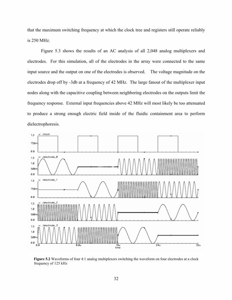
Figure 5.3 shows the results of an AC analysis of all 2,048 analog multiplexers and
electrodes. For this simulation, all of the electrodes in the array were connected to the same
input source and the output on one of the electrodes is observed. The voltage magnitude on the
electrodes drop off by -3db at a frequency of 42 MHz. The large fanout of the multiplexer input
nodes along with the capacitive coupling between neighboring electrodes on the outputs limit the
frequency response. External input frequencies above 42 MHz will most likely be too attenuated
to produce a strong enough electric field inside of the fluidic containment area to perform
dielectrophoresis.
Figure 5.2 Waveforms of four 4:1 analog multiplexers switching the waveform on four electrodes at a clock frequency of 125 kHz
32

Figure 5.3 Frequency response of electrodes. Large fanout of multiplexer input nodes and capacitive coupling of neighboring electrodes results in a -3dB frequency of 42 MHz.
Table 5.1 summarizes the average power consumption of the lab-on-a-chip. The power
consumed is primarily due to the clock tree and array of shift registers. The analog frequencies
commonly used for dielectrophoresis are relatively low (kHz to low MHz). Therefore, as can be
seen in the table, the power consumption of the chip is expected to be fairly small
Table 5.1 Average power consumption of 3D lab-on-a-chip
Clock Frequency Average Power
25 kHz 330 µW 250 kHz 646 µW 2.5 MHz 3.36 mW 25 MHz 183 mW
250 MHz 1.73 W
From the simulations presented in this section we learn what voltage waveforms can be
placed on the electrodes. In the next section, we use this information to perform a finite element
analysis of the dielectrophoresis fields.
33

5.2 FINITE ELEMENT ANALYSIS OF DIELECTROPHORESIS FIELDS
Figure 5.4 shows the results of a 2D COMSOL finite element analysis of an electric field created
inside of the trench by the electrodes. The conductivities and permittivities of the oxide layer
and polysilicon electrodes are assigned values that reflect their material properties. The boundary
condition at the top of the trench is set to be a grounded reference plane. Grounding the top
surface of the fluid containment area both increases the magnitude of the intensity gradient
( ) and results in more distinctly shaped electric field peaks and valleys. The electrode in
the center of figure 5.4 is assigned a voltage of 1.5 V, while the remaining electrodes are
grounded. This configuration creates an electric field maximum above the center electrode. The
2RMSE∇
Figure 5.4 Electric field with single maximum. All electrodes except for centermost are grounded. Center electrode set to 1.5 V. Arrows show direction of intensity gradient.
arrows in figure 5.4 show the direction of the term. The force vector will be directed
along these same paths in the case of particles undergoing positive dielectrophoresis, trapping
2RMSE∇ DEPF
r
34

them in the region above the center electrode. Figure 5.5 is a plot from the same simulation with
the scale adjusted so that electric field can be seen within the trench but not around the
electrodes. The magnitude of the electric field at the oxide/fluid interface is 5.3x10⁴ Vm-1. This
shows that even though the electrodes are separated from the fluidic medium by an insulating
dielectric, the separation distance is small enough to support the creation of considerable electric
fields within the trench.
Figure 5.5 Profile of single-maximum electric field in center of trench area. Electric field magnitude at oxide-fluid interface above the center electrode is 5.3x10⁴ Vm-1.
Figure 5.6 shows the results of another 2D analysis in which each of the electrodes
alternate between 1.5 V and ground. This electrode configuration in turn creates a pattern of
alternating minima and maxima along the bottom surface of the trench. Particles undergoing
dielectrophoresis in this case will be trapped along the bottom surface in a similar periodic form.
The center-to-center pitch of the trapping points is 900 nm. This simulation is an example of an
35

electric field profile that can be used to create the particle-based grating structures discussed in
section 4.2 and is the basis of the optical simulations presented in section 5.7.
Figure 5.6 Alternating electric field minima and maxima created along bottom surface of trench by alternating voltages on neighboring electrodes between 1.5 V and ground. Arrows show direction of intensity gradient.
The simulations shown in figures 5.7(a) – 5.7(c) demonstrate how the electrodes can be
time-sequenced to deterministically move particles. The sequence begins by creating a single
electric field minima in the center of the trench (figure 5.7(a)), trapping particles in that area.
For these simulations, the electrodes were configured to create electric field minima because
negative dielectrophoresis is the most stable way to trap a particle [12]. Figures 5.7(b) and 5.7(c)
show how the electrodes can be progressively activated in a shift-register fashion to create
moving traps that the particles will follow. The amount of time it takes to complete this sequence
depends on the velocity of the particles, which is examined in the simulations of section 5.6.
36

Figure 5.7(a). The Single negative dielectrophoresis trap in center will attract particles to the region above it. The arrows show direction of dielectrophoretic force vector. Electrode polarity annotated on bottom of plot.
Figure 5.7(b). The change in electrodes polarity causes the location of the electric field minima to change
Figure 5.7(c). The particles new steady-state position shifted over 450 nm to the right by time sequencing the electrode polarities in a shift-register fashion.
37

For the electric field simulations presented in this section, the reference plane at the top
of the trench is immersed in the medium and since buffer solutions used to contain biological
media are usually conductive, joule heating of the fluid can occur. Joule heating of the aqueous
medium will result in a thermally induced fluid flow that will exert additional drag force on the
manipulated particles. We examine these factors in the following sections.
5.3 FINITE ELEMENT ANALYSIS OF TEMPERATURE GRADIENTS
The combination of an intense electric field inside of a conductive medium results in joule
heating [14]. Heat is generated by power that is dissipated within the trench area. The
volumetric power dissipation is given by the equation [14]:
( )32 −⋅= mWEW mm σ (5.1)
Figure 5.8 shows the temperature distribution resulting from the electric field profile
shown in figure 5.7(a). This simulation is done using the COMSOL heat transfer finite element
solver. For this analysis, the nominal temperature of the medium is set to 300 K, the thermal
conductivity of the KCL buffer solution [32] is 0.61 W·m-1·K-1 and the expression for Wm is used
as the heat source. The density and heat capacity of the solution are assigned values identical to
water (1000 kg·m-3 and 4.72 kJ·kg-1·K-1). The temperature distribution varies from 300.000 K to
300.003 K. Since the temperature does not vary much, the magnitude of the electro-thermal
forces associated with this gradient will be small. This temperature profile is used in the next
section to calculate the velocity of the thermally induced fluid motion.
38

Figure 5.8 Temperature variations due to joule heating of fluid immersing the reference plane
5.4 CALCULATION OF FLUID VELOCITY PROFILE
The temperature field shown in figure 5.8 generates gradients in σm and εm, giving rise to an
electrical body force on the fluid and resulting in additional drag force on the particles. Figure
5.9 shows the direction of Fthermal in this case. In order to capture a profile of the stirring motion
this force induces in the medium, the Navier-Stokes equations have to be solved with Fthermal as
the volume force term. However, since the profile presented in this section is the result of a DC
electric field we can simplify the model with an approximation. At low frequencies, the
coulombic force dominates the thermally induced fluid motion. Therefore, the magnitude of the
fluid velocity (vmax) can be approximated by the equation [17]:
T1
dkV
105v m
memm
4emm4
max ∂∂
×≈ − σση
σε (5.2)
39

where km is the thermal conductivity of the medium, de is the distance from the electric field
peak, Ve is the voltage difference across the electrodes (in our case Ve is adjusted to account for
the reduction of the electric field by the oxide layer) and T
1 m
m ∂∂σ
σ ≈ 0.02K-1 for electrolytic
solutions [17].
Figure 5.9 Direction of electro-thermal force vector (Fthermal ) within the trench area
Theoretically this expression goes to infinity as de→0. However, equation (5.2) has been
shown to agree with finite element calculations if de is set to a value that is approximately equal
to the length of the gradient [17], which is on the order of 1 µm in this simulation. This
approximation results in a maximum fluid velocity of 1x10-15 µm·s-1 in the direction of Fthermal.
The simulation results presented in section 5.6 show that the velocity of the particles due to
dielectrophoresis is many orders of magnitude greater that this thermally induced fluid velocity.
Therefore, the additional drag force exerted by this flow does not significantly alter the motion of
the particles.
40

5.5 VIRTUAL-WORK CALCULATION OF ELECTRICAL FORCES
While the expression for given in equation (2.4) provides insight on how the particle
interacts with its surrounding medium, it is a derivation of force based on the assumption that the
electric field does not change significantly over the length of the particle [12]. This assumption is
not valid when the radius of the particle is on the same order of magnitude as the gap spacing
between trapping electrodes. When they are similar in dimension, as is the case for the
simulations presented in this chapter, a more rigorous analysis is required. Therefore, we used a
simulator with the capability to accurately predict values of the dielectrophoretic force vector
using the virtual-work method [36]. In order to predict how a KSHV virion will respond to
dielectrophoresis using this method, we first have to model its electrical properties.
DEPFr
5.5.1 Electrical Modeling of KSHV Particles
Previous research has shown the use of dielectrophoresis to manipulate herpes simplex virions
[27,33,34,35]. Since KSHV is very similar in its physical structure to HSV, we used the same
electrical model as in reference [27] for this work. Figure 5.10 shows the physical structure of
the virion, or complete virus particle, is modeled as two concentric shells, as depicted by figure.
The outside layer is an approximately 20 nm thick insulating shell, referred to as the lipid
bilayer. That shell encloses a thick conductive gel called the tegument. The lipid bilayer is
modeled as having a surface conductance of 10 nSm-1 and permittivity of 10ε0. The electrical
properties of the tegument are modeled as having a conductivity of 0.005 Sm-1 and permittivity
of 70ε0. The physiological buffer used in this model is a KCL solution with conductivity of 0.1
41

Sm-1 and permittivity of 78ε0. Using a medium that is more conductive than the virions ensures
that the particles will undergo negative dielectrophoresis at low frequencies.
Figure 5.10 KSHV virion modeled as two concentric shells. The outer layer, the lipid bilayer, is an insulating shell that surrounds a conductive inner core, the tegument.
5.5.2 Virtual Work Calculation of Dielectrophoretic Force Vector
Figure 5.11 shows the model used in the Ansoft Maxwell finite-element solver to calculate the
electrical force exerted on the particle. The KSHV shell-model, polysilicon electrodes, oxide
layers and fluidic medium are all included in the model. Because of the presence of the particle,
the model is no longer infinitely symmetric in the third dimension (x-axis in figure 5.11), making
it necessary to do the simulations in 3D. The simulations are done by traversing the KSHV
model in 250 nm increments throughout every point in the medium, re-meshing and resolving
the model at each step. Since the electric field is uniform across the third dimension, there is no
dielectrophoretic force along that axis and the particle is not traversed there. In the case of the
electric field profile shown in figure 5.7(a), the magnitude of the dielectrophoretic force ranges
on the order of 10-14 N to 10-16 N, depending on its proximity to the electric field minima.
42

Figure 5.11 3D model used to calculate dielectrophoretic force vector using the virtual-work method
The virtual-work method is a very accurate approach to calculating electrical forces [36]
but, it is computationally expensive. It takes 4 days running on a workstation with dual 2.2 GHz
Intel Xeon processors and 4GB of RAM to evaluate the force vector at all 328 points in the
space.
5.6 DISCRETE-TIME SIMULATION OF PARTICLE MOTION
We created a custom particle-motion simulator using Matlab that incorporates all of the forces
described in chapter 2. These forces were either imported from simulation or calculated directly.
Using a time-based simulator allows us to observe the movement of the virus models and the
speed at which they travel.
43

The basis of the motion simulator are Newton’s laws of motion, which in the case of a
particle moving in our system can be written as
dtdv
mFF ppdragext =− (5.3)
where Fext = FDEP + Fbrownian + Fthermal+ Fbuoyancy and mp is the mass of a KSHV virion. Solving
for the velocity of the particle vp by separation of variables gives
( )pm
extm
t
pm
extmpp r6
Fver6
Fv0vv p
πηπητ ++⎟
⎟⎠
⎞⎜⎜⎝
⎛−−=
− (5.4)
pm
pp r6
mπητ = (5.5)
The mass of a KSHV virion is mp ≈ 3.3x10⁻¹⁹ kg [10], resulting in a time constant of τp ≈158 ps.
The typical observation period for dielectrophoresis of small particles is on the order of seconds
[17], which is much greater than the time constant. Therefore, the acceleration terms in equation
(5.4) can be neglected and the particle can be considered to move at its terminal velocity:
pm
extmp r6
Fvv
πη+= (5.4)
This is in agreement with what is mentioned in section 2.1.1 about inertia being negligible for
particles with very low Reynolds numbers.
44

Figures 5.12(a) through 5.12(d) show the results of a motion simulation in which a large
concentration of virions are randomly placed inside of the trench. The electric field profile used
in this simulation is the same as the one shown in figure 5.6, the voltages on each of the
electrodes alternate between 1.5 V DC and ground. Because the electric field does not vary
along the axis parallel to the electrodes, this profile was extruded into the third dimension.
Figure 5.12(a) shows the distribution of the particles at time t = 0 s. As seen in figure 5.12(d), the
particles reach their steady-state by t = 16 s and remain trapped after that. The average velocity
of the particles is approximately 0.12 µm·s-1 and their motion is not significantly affected by
Brownian motion, joule heating or buoyancy effects.
Figure 5.12(a) Initial position of particles (t = 0 s)
Figure 5.12(b) Distribution of particles at t = 7 s
45

Figure 5.12(c) Distribution of particles at t = 11 s
Figure 5.12(d) Distribution of particles for t > 16 s
The optical characteristics of the steady state arrangement of particles shown in figure
5.12(d) is analyzed in the next section.
46

5.7 RIGOROUS COUPLED WAVE ANALYSIS OF GRATINGS
In this section, we characterize the diffraction efficiency of the particle grating structures. Since
the grating has a multi-layered profile, its optical characteristics are complex. Therfore, we
performed a rigorous coupled wave analysis (RWCA) of the structure using the RSOFT
DiffractMOD software package to accurately calculate efficiency. Figure 5.13 shows a cross-
sectional view of the RSOFT model. The RWCA algorithm assumes the diffractive structure is
infinitely periodic in one or more dimensions, so it only requires information about one period of
the grating structure to calculate how the light diffracts, however figure 5.13 includes multiple
periods for clarity.
Figure 5.13 Multi-layered grating structure used in rigorous coupled wave analysis. The period of the trapped virus particles is set to 900 nm, while the index modulation depth, w, is varied. Indices of refraction for each layer annotated on left hand side of figure.
47

The incident light is a single-wavelength plane wave that propagates through layers
representing air, the glass lid, the buffer solution, the chip oxide layers, polysilicon electrodes
and trapped virus particles. The angle of incidence is 00 with respect to the normal plane of the
trapped particles. Since the index of refraction for KSHV particles is not readily available, the
value used in this model, nvirus = 1.57, is taken from a similar virus for which this data is
published [37]. For the RWCA simulations presented in this chapter, the period of trapped
particles is set to 900 nm, which corresponds with the electric field profile seen in figure 5.6 and
used in the simulation of figure 5.12.
5.7.1 2D Diffractive Analysis
The first step of the analysis is the selection of the incident wavelength. For a 00 incident angle,
the wavelength is bounded by equation (4.1) to md
<λ . However, care must be taken not to
select too short of a wavelength. This is demonstrated by the simulation results shown in figure
5.14(a). Figure 5.14(a) is a plot of reflected power, relative to the input power, versus the angle
of observation. The discrete diffraction orders are annotated on the graph. For this simulation,
the width of the trapped particle region is 250 nm and the incident wavelength is 200 nm. Such a
short wavelength leads to multiple unwanted diffraction orders that disperse energy at very wide
angles. Using ultraviolet light in this case also gives rise to reflected orders due diffraction off of
the electrode array, because it too is a periodic modulation of the index of refraction. Both of
these effects can be avoided by selecting a longer wavelength.
Figure 5.14(b) shows results from the same simulation with the incident wavelength
changed to 500 nm. Only one diffraction order {-1, 1} due to the trapped particles can
48

physically exist at this wavelength. The reflected power of this order is 13.8% of the input
power and is observed at an angle of 33.750. Since periodicity of the dielectrophoretic traps is a
controlled variable, the existence of this order can be used as indicator of whether or not virus
particles are present.
Figure 5.14(a) Reflected diffraction efficiency versus of observation angle for w = 250 nm and λ=200 nm. Multiple unwanted orders exist due to short wavelength and diffraction off of electrode array. Discrete diffraction order annotated on plot.
Figure 5.14(b) Reflected diffraction efficiency for w = 250 nm and λ=500 nm. Only one reflected order {-1,1} exists due diffraction off of trapped particles.
49

Figure 5.15 shows the results of multiple simulations in which the width of the cross-
sectional area of the particles is varied. The diffraction efficiency gradually increases as with the
area and reaches peak at w ≈ 400 nm. The maximum diameter of a KSHV particle will most
likely be smaller than this peak. Therefore, if it is assumed the particles are trapped in a single-
file line, the graphs of figure 5.15 can be used a tuning-curve to create a mapping between the
average size of the trapped particles and diffraction efficiency.
This change in efficiency can be measured in a laboratory environment by observing the
decrease in power at the 0th order, which corresponds to light undergoing specular reflection.
Likewise the increase in power of the {-1,1} reflected order can be detected.
Figure 5.15 Reflected diffraction efficiency versus cross sectional area of trapped particle regions.
The simulations presented in this section are based on assumption that the optical model
of figure 5.13 can be extruded infinitely into the third dimension. If the concentration of
50

particles in the buffer solution is low enough, this assumption is not valid. We examine this
situation in the next section by performing 3D RWCA simulations.
5.7.2 3D Diffractive Analysis
In order to perform a 3D analysis, we used the same model of figure 5.13 and specified lengths
for the third dimension. Because RWCA can only simulate structures that are infinitely periodic
in all but one dimension, the change in particle concentration is modeled by varying the
periodicity of particles along that third axis (z-axis). Figure 5.16 shows how the structure of the
diffraction grating will be significantly changed depending on the concentration of particles in
the solution. If the concentration is significantly low, then the particles will no longer form solid
lines.
Figure 5.16 Depiction of the difference in the structure of the nanoparticle diffraction grating based on the concentration of particles
Figures 5.17(a) through 5.17(b) are grids that show reflected efficiency versus the
diffraction order at which it is found. The scales are adjusted so that all the present orders can be
seen. In the simulation of figure 5.17(a), w = 250 nm, λ = 500 nm and the period of the particles
on the z-axis is 0 nm. This corresponds exactly to the 2D example presented in figure 5.14(b).
and only the (0,1), (0,0), (0,-1) diffraction orders are present. The periodicity of the particles
51

along the z-axis is increased to 571 nm and 800 nm in figures 5.17(b) and 5.17(c). These
changes result in the existence of new diffraction orders that can be used to estimate particle
concentration. For example, the change from the particles not being periodic along z to a
periodicity 571 nm (5.17 (b)) resulted in the addition of the (-1,0), (1,0) orders to the diffraction
pattern.
Figure 5.17(a). Diffraction order vs. efficiency for w=250 nm, λ=500 nm. Period of particles along z-axis is 0 nm.
Figure 5.17(b). Periodicity of trapped particles along z-axis changed to 571 nm.
52

Figure 5.17(c). Periodicity of trapped particles along z-axis changed to 800 nm.
53

6.0 POST-FABRICATION PROCEDURES FOR 3D LAB-ON-A-CHIP
There are several post processing steps that will need to be completed after the chip has been
fabricated and prior to testing its functionality. First, the top level metal will be etched away in
order to form the microfluidic trenches used for solution containment. A lithographic mask will
be used to coat the top surface of the chip with photoresist and the trench areas will be revealed
by way of exposure to UV light. The top metal will be removed by using a wet chemical etch,
with the oxide layer on the bottom and sidewalls of the trench acting as the etch stop.
If we find that the efficiency of the naturally reflected diffraction orders are too low, our
next step will be to coat the bottom surface of the fluidic containment areas with a high-reflective
dielectric thin-film. The deposition of such a thin-film would bring the reflectivity of the oxide
surface within the 90% to ~100% range [38], greatly improving the signal-to-noise ratio of the
measured intensity.
The chip will not be placed in an IC package, but will be affixed directly to a custom
PCB with an epoxy. All 34 of the electrical I/O contacts will be made from the chip to the board
using a manual wire bonder (See appendix B for complete chip pinout).
The final steps before testing the functionality of the chip will be to fill the on-chip trench
with the aqueous medium and particles of interest. Current pressure-regulated microinjectors are
capable of injecting and vacuuming volumes as small as femtoliters [XX]. Since the volume of
the trench in our design is 400 picoliters, we will require the use such a microinjection system.
54

The microfluidic channel will then be sealed with a conductive glass lid that will be used as the
reference plane.
6.1 TEST PLAN
One goal of labs-on-chips is to be able to integrate as many laboratory functions as possible onto
one device. As the complexity of these chips increases, so does the number of things that can
lead to their failure. Therefore, it is essential to have a thorough test plan for initial prototypes.
The first functional test we carry out will determine if the digital circuitry is alive and
working. We will load the chain of shift registers with a pattern of alternating 1’s and 0’s. An
output pad is connected to the output of the last register in the chain so that it can be observed on
an oscilloscope. This pad will not be wire bonded to the PCB but will be probed using a
micropositioner. If the same pattern that was initially loaded is observed on the output, then we
will be able to conclude that the clock tree is functioning properly and that we are able to
successfully write both 1’s and 0’s to each bit of each shift register.
The first test of the chips ability to manipulate particles will be done with latex spheres
that are approximately 250 nm in diameter. We chose to experiment first with latex particles
because they are easier to obtain and require less effort to handle than live virions. Manufactured
particles also have less variation in size when compared to a sample of living organisms,
therefore, the response of each particle to dielectrophoresis will be more predictable. Previous
work [34] has shown that when spheres of this type and dimension are placed between out-of-
phase electrodes in a KCL solution with a conductivity of 250 µSm-1, they will experience
positive dielectrophoresis at a frequency of 1 MHz. We will use this setup as our starting point.
55

If no movement is detected using these parameters, we will be able to sweep the frequency
and/or adjust the conductivity of the KCL solution. We will avoid the need for electron
microscopy to detect particle movements by fluorescently marking the spheres and observing
collections of particles with an optical microscope.
The next experiment will measure the diffraction efficiency of the trapped particles.
Figure 6.1 shows the setup that will be used to test the efficiency [30]. The monochromator will
filter the desired wavelength from the light source and the collimator will then direct the beam
towards the grating. The incident light will be polarized to help eliminate reflections from the
fluidic medium on the chip and its glass lid. The light will then pass through an aperture,
truncating the beam to a width that is appropriate for the grating. The diffracted orders will be
converted to an electrical signal by the detector and after amplification, will be compared to a
directly measured reference signal in order to evaluate the grating efficiency.
Figure 6.1 Setup for measuring diffraction efficiency of gratings
The final test will be a repetition of these experiments with KSHV virions. Experimental
results [27] have shown that when HSV particles are placed in a mannitol solution of
conductivity 0.005 Sm-1, the particles will transition from undergoing positive to negative
dielectrophoresis in the frequency in the range of 4 to 5 MHz, which is well within the operating
56

range of the circuitry on the 3D lab-on-a-chip. Once we reach this phase of testing, collaboration
with molecular virologists will be required for assistance with the handling of KSHV particles.
57

7.0 SUMMARY
The design of a lab-on-a-chip in 3D integrated circuit technology is presented in this thesis. The
main features of the chip are summarized by table 7.1. The lab-on-a-chip has the capabilities to
manipulate nanometer scale particles by way of dielectrophoresis. We take advantage of features
inherent to 3D chip-making technology to create an on-chip microfluidic trench with an
extremely dense electrode array under it. In addition to the components necessary for
dielectrophoresis, we also integrate analog and digital electronics onto the chip. We also
demonstrate in this thesis a new technique for detecting manipulated particles by arranging them
into diffraction grating structures. We verify the operation of the lab-on-a-chip by performing a
simulation study of its capabilities to manipulate KSHV virus particles and have them optically
detected. We also give a plan for the post-fabrication steps and testing procedures that will be
done on the initial prototype devices.
Table 7.1 Summary of 3D lab-on-a-chip specifications
Technology 3D 0.18µm SOI Power supply 1.5V Chip area 2x4 mm2
# of dielectrophoresis electrodes 2,048 Electrode width 180 nm Electrode center-to-center pitch 450 nm
58

7.1 CONCLUSIONS
In this section, we present our conclusions about the lab-on-a-chip design, our optical detection
scheme and the simulation flow we used. Our lab-on-a-chip is the first ever to be designed in 3D
integrated circuit technology and clearly shows the benefits of doing so. With this technology,
we were able to create the most dense electrode array ever to be designed in a CMOS compatible
process. In addition, our design does not require cumbersome post-processing steps for creating
on-chip microfluidic channels. Also, having the capability to directly integrate a large amount of
digital and analog electronics on to the chip makes it tremendously flexible; allowing it to be
adapted to many applications even after it has been fabricated. All of these features make 3D
chip stacking technology a promising platform for lab-on-a-chip design.
The technique we developed for detecting small particles is especially well-suited for lab-
on-a-chip devices. This method of sensing is not tied to the design we presented here; it can be
utilized with any lab-on-a-chip that has the capabilities to arrange particles into a grating-like
form. Also, our technique has the added benefit that it does not require extra preparation of the
sample-under-test, which is highly undesirable in the case of biological particles. Our sensing
mechanism has the additional benefit of being relatively inexpensive; the optical components
needed to implement our scheme have a price that is comparable to the low-cost optics found in
modern CD players.
Due to the multidisciplinary nature of our chip, we had to research the fields of biology,
chemistry, optics, fluid mechanics, thermodynamics, electrostatics, and electronic design. The
design of this chip is a reminder that very few, if any, microsystem designers are experts in all of
these fields. Therefore, we realize that there is a need for CAD tools to help with the end-to-end
design of such multi-domain mixed-signal microsystems. The current methodology is to use a
59

different tool for each domain present and then stitch together the results using an additional tool,
in our case Matlab. This process is time consuming, and in some cases, inefficient and will need
to be addressed when such technologies such as labs-on-chips become more widespread.
7.2 FUTURE WORK
The short-term future work associated with this thesis is the improvement of our simulation flow.
The first of which is the modeling of the dielectrophoretic force. Some have suggested [39]
modeling the particle as a multi-pole rather than dipole. This raises the question, would doing so
strike enough balance in the computation time/accuracy tradeoff that we could eliminate timely
virtual-work computations? Also, there are other forces in action that are not included in our
models. For example, researchers have shown that there exists a particle to particle interaction
force that causes pearl-like chaining of the particles [40]. There also exists an AC osmotic force
on the fluid that is associated with the electrical double layer at the interface of the medium [17].
The temperature gradients cause dynamic changes in the viscosity and density of the medium.
We have included a few secondary forces in this work (electro-thermal effect, Brownian motion
and buoyancy) and have found them to be insignificant but, is the aggregate effect of all these
minor forces enough to significantly change the motion of the particles? There are also
limitations to the optical simulations we performed. We were restricted by the tools we used to
simulating infinitely periodic diffractive structures. However in reality, if the concentration of
the particles is relatively low, chances are each row of trapped particles will look somewhat
different. If that is the case, will there still be some sort of diffraction pattern due to the particles
that we can detect and does there exist an efficient way to simulate it?
60
In addition to our test plan (chapter 6), there are many other tests we can perform because
of the flexibility of our design. We’ve essentially created a test-bed with the ability to perform
multiple types of dielectrophoresis experiments. For example, we could carry out traveling wave
dielectrophoresis [41], field-flow fractionation [42], or multi-frequency dielectrophoresis
experiments [50]. One future possibility stemming from our work could be the characterization
of the optical properties of virus particles. There is very little published information about
properties such as the index of refraction of virus particles. Our chip could be used to initiate
new research and lead to new types of optical biological sensors.
Finally, our long term goal is to find specific applications for our 3D lab-on-a-chip. For
example, we could possibly develop a blood filtration device that is programmed to route “bad”
particles in one direction and “good” particles in another. If we do further research on scaling
down our particle detection method and develop a way to get that information on to the chip, we
can implement much more elaborate systems. An example of this could be a wearable device
that monitors a patient for a certain type of virus. Such a device could possibly use
dielectrophoresis to attract viruses to certain locations, use the feedback from the sensor to do a
sophisticated analysis of the viruses with its integrated microprocessor and then alert the patient
that he needs to increase his medication dosage to a certain level or maybe even rush to the
hospital! The future possibilities for microsystems like our 3D lab-on-a-chip are both numerous
and promising.
61

APPENDIX A
3D INTEGRATED CIRCUIT PROCESS DESIGN LAYERS
Figure A.1 Cross-section of design layers in Lincoln Labs 0.18 µm 3D SOI process [21]
62

APPENDIX B
3D LAB-ON-A-CHIP PINOUT
Figure B.1 Pinout of 3D Lab-on-a-chip
63
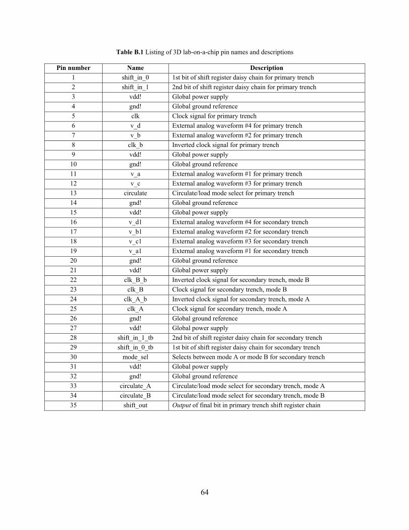
Table B.1 Listing of 3D lab-on-a-chip pin names and descriptions
Pin number Name Description 1 shift_in_0 1st bit of shift register daisy chain for primary trench 2 shift_in_1 2nd bit of shift register daisy chain for primary trench 3 vdd! Global power supply 4 gnd! Global ground reference 5 clk Clock signal for primary trench 6 v_d External analog waveform #4 for primary trench 7 v_b External analog waveform #2 for primary trench 8 clk_b Inverted clock signal for primary trench 9 vdd! Global power supply
10 gnd! Global ground reference 11 v_a External analog waveform #1 for primary trench 12 v_c External analog waveform #3 for primary trench 13 circulate Circulate/load mode select for primary trench 14 gnd! Global ground reference 15 vdd! Global power supply 16 v_d1 External analog waveform #4 for secondary trench 17 v_b1 External analog waveform #2 for secondary trench 18 v_c1 External analog waveform #3 for secondary trench 19 v_a1 External analog waveform #1 for secondary trench 20 gnd! Global ground reference 21 vdd! Global power supply 22 clk_B_b Inverted clock signal for secondary trench, mode B 23 clk_B Clock signal for secondary trench, mode B 24 clk_A_b Inverted clock signal for secondary trench, mode A 25 clk_A Clock signal for secondary trench, mode A 26 gnd! Global ground reference 27 vdd! Global power supply 28 shift_in_1_tb 2nd bit of shift register daisy chain for secondary trench 29 shift_in_0_tb 1st bit of shift register daisy chain for secondary trench 30 mode_sel Selects between mode A or mode B for secondary trench 31 vdd! Global power supply 32 gnd! Global ground reference 33 circulate_A Circulate/load mode select for secondary trench, mode A 34 circulate_B Circulate/load mode select for secondary trench, mode B 35 shift_out Output of final bit in primary trench shift register chain
64

BIBLIOGRAPHY
1. Pohl, Herbert A. “The Motion and Precipitation of Suspensoids in Divergent Electric Fields”, J. Appl. Phys. 22, 869, 1951
2. Ghallab,Y.;Badawy,W., “Sensing methods for dielectrophoresis phenomenon: From bulky instruments to lab-on-a-chip”, Circuits and Systems Magazine, IEEE, Vol.4, Iss.3, Third Quarter 2004, pp: 5- 15
3. Hughes, Michael Pycraft, “AC electrokinetics: applications for nanotechnology”, Nanotechnology, 11, pp. 124-132 , 2000
4. Gambari R, Borgatti M, Altomare L, Manaresi N, Medoro G, Romani A, Tartagni M, Guerrieri R., “Applications to cancer research of "lab-on-a-chip" devices based on dielectrophoresis(DEP)”,Technol. Cancer Res. Treat. 2003 Feb;2(1):31-40
5. Huang, Y., Yang, J., Wang, X. B., Becker, F. F., Gascoyne, P. R., “The removal of human breast cancer cells from hematopoietic CD34+ stem cells by dielectrophoretic field-flow-fractionation.” J Hematother Stem Cell Res., 1999, Oct;8(5):481-90.
6. Xu, C., Wang, Y., Cao, M., Lu, Z. “Dielectrophoresis of Human Red Cells in Microchips.” Electrophoresis 20, 1829-31,1999.
7. Paul Yager, Thayne Edwards, Elain Fu, Kristen Helton, Kjell Nelson, Milton R. Tam and Bernhard H. Weigl “Microfluidic diagnostic technologies for global public health”, Nature 442, 412-418(27 July 2006)
8. Chang, Y., Cesarman, E., Pessin, M. S., Lee, F., Culpepper, J., Knowles, D. M., and Moore, P. S.. “Identification of herpesvirus-like DNA sequences in AIDS-associated Kaposi's sarcoma”. Science. 265, 1865-69, (1994).
9. http://en.wikipedia.org/wiki/Kaposi's_sarcoma-associated_herpesvirus
10. Trus B.L., et al. “Capsid structure of Kaposi’s sarcoma-associated herpesvirus, a gammaherpesvirus, compared to those of an alphaherpesvirus,herpes simplex virus type 1, and a betaherpesvirus”, cytomegalovirus. J. Virol. ,2001
65
11. Saliterman, S., Fundamentals of BioMEMS and Medical Microdevices, SPIE Press, 2006.
12. T.B. Jones, Electromechanics of Particles, Cambridge Univ. Press, 1995.
13. N. G. Green, A. Ramos, A. González, H. Morgan, and A. Castellanos, “Fluid flow induced by nonuniform ac electric fields in electrolytes on Experimental measurements microelectrodes”. I., Phys. Rev. E 61, 4011 (2000)
14. A Ramos, H Morgan, N G Green and A Castellanos, “Ac electrokinetics: a review of forces in microelectrode structures”, J. Phys. D: Appl. Phys. 31 2338-2353, 1998
15. Einstein, A.,“The theory of the brownian movement” ,Ann. der Physik, vol.17,1905
16. Green, NG and Ramos, A. and Morgan, H, “AC electrokinetics: a survey of sub-micrometre particle dynamics”, J. Phys. D: Appl. Phys, vol. 33, 2000
17. Castellanos, A. and Ramos, A. and Gonzalez, A. and Green, N.G. and Morgan, H,
“Electrohydrodynamics and dielectrophoresis in microsystems: scaling laws”, Journal of Physics D: Applied Physics, vol 36, no. 20, 2003
18. E. M. Purcell, “Life at low Reynolds number”, American Journal of Physics Jan. 1977 Vol. 45 Issue 1, pp.3-11
19. Panton, Ronald, L. Incompressible Flow, third edition, Wiley, 2005.
20. Nicolas G. Green, Antonio Ramos, Antonio Gonzalez, Antonio Castellanos and Hywel Morgan, “Electrothermally induced fluid flow on microelectrodes”, Journal of Electrostatics, Volume 53, Issue 2, August 2001, Pages 71-87.
21. MIT Lincoln Laboratory. MITLL Low-Power FDSOI CMOS Process Design Guide, September, 2006.
22. Manaresi, N.; Romani, A.; Medoro, G.; Altomare, L.; Leonardi, A.; Tartagni, M.; Guerrieri,R., “A CMOS chip for individual cell manipulation and detection” Solid-State Circuits, IEEE Journal of, Vol.38, Iss.12, Dec. 2003 Pages: 2297- 2305
23. Enteshari, A.; Jullien, G.A.; Yadid-Pecht, O.; Kaler, K.V.I.S. “All CMOS low power platform for dielectrophoresis bio-analysis” Solid-State Circuits Conference, 2005. ESSCIRC 2005,Vol.,Iss.,12-16,Sept.2005
24. Lifeng Zheng; Shengdong Li; Burke, P.J.; Brody, J.P., “Towards single molecule manipulation with dielectrophoresis using nanoelectrodes”,. IEEE-NANO. Vol.1, Iss., 12-14 Aug. 2003
66

25. Cui, L. and Zhang, T. and Morgan, H, “Optical particle detection integrated in a dielectrophoretic lab-on-a-chip.” Journal of Micromechanics and Microengineering, vol. 12, no. 1,2002
26. Green, N. G., H. Morgan, and J. J. Milner. “Manipulation and trapping of submicron bioparticles using dielectrophoresis”. J. Biochem. Biophys. Methods. 35:89-102, 1997
27. Hughes, M. P., H. Morgan, F. J. Rixon, J. P. H. Burt, and R. Pethig.. “Manipulation of herpes simplex virus type 1 by dielectrophoresis”. Biochim. Biophys. Acta. 1425:119-126, 1998
28. Kentsch, J.; Durr, M.; Schnelle, T.; Gradl, G.; Muller, T.; Jager, M.; Normann, A.; Stelzle, “Microdevices for separation, accumulation, and analysis of biological micro- and nanoparticles” Nanobiotechnology, IEE Proceedings, Vol.150, Iss.2, 1 Nov. 2003
29. Bakewell, DJ and Morgan, H., “Quantifying dielectrophoretic collections of sub-micron particles on microelectrodes”, Measurement Science and Technology, vol. 15, no.1, 2004
30. Palmer, Christopher. Diffraction Grating Handbook, 6th edition, Newport Corporation (2005).
31. Serway, Raymond. Physics For Scientist and Engineers with Modern Physiscs, 3rd edition, Saunders College Publishing, (1990)
32. Ramires M.L.V, Nieto de Castro C.A, “Thermal Conductivity of Aqueous Potassium Chloride Solutions”, International Journal of Thermophysics, vol. 21, May 2000
33. Michael P. Hughes, Hywel Morgan and Frazer J. Rixon, “Measuring the dielectric properties of herpes simplex virus type 1 virions with dielectrophoresis”, Biochimica et Biophysica Acta, Volume 1571, Issue 1, 10 May 2002, Pages 1-8.
34. Morgan, H. and Hughes, M.P. and Green, N.G., “Separation of Submicron Bioparticles by Dielectrophoresis”, Biophysical Journal, vol. 77, no. 1, 1999
35. Hughes, M.P. and Morgan, H. and Rixon, F.J., “Dielectrophoretic manipulation and characterization of herpes simplex virus-1 capsids”, European Biophysics Journal, vol. 30, no. 4, 2001
36. J. L. Coulomb and G. Meunier, “Finite element implementation of virtual work principle for magnetic or electric force and torque computation,” IEEE Trans. Magn., vol. 20, pp. 1894–1896, Sept. 1984.
37. Oster, G., “Two-Phase Formation In Solutions Of Tobacco Mosaic Virus and the Problem Of Long-Range Forces”, The Journal of General Physiology, vol. 33, no. 5, 1950
67

38. http://en.wikipedia.org/wiki/Dielectric_mirror
39. Jones, T.B., “Basic Theory of Dielectrophoresis and Electrorotation”, IEEE Engineering In Medicine and Biology Magazine, vol. 33, 2003
40. Kadaksham, A.T.J. and Singh, P. and Aubry, N., “Dielectrophoresis of nanoparticles”, Electrophoresis, vol. 25, no. 21-22, 2004
41. Hagedorn, R. and Fuhr, G. and Muller, T. and Gimsa, J., “Traveling-wave dielectrophoresis of microparticles”, Electrophoresis, vol. 13, no. 1-2, 1992
42. Huang, Y. and Wang, XB and Becker, FF and Gascoyne, PR. “Introducing dielectrophoresis as a new force field for field-flow fractionation”, Biophysical Journal, vol. 73, no. 2, 1997
43. Huang, Y. and Wang, XB and Becker, FF and Gascoyne, PR. “Introducing dielectrophoresis as a new force field for field-flow fractionation”, Biophysical Journal, vol. 73, no. 2, 1997
44. Yager,P., “Microfluidic diagnostic technologies for global public health”, Nature, July 2006
45. http://cels.uri.edu/news/archive/NewsNSF.html
46. Dittrich, P. and Manz, A., “Lab-on-a-chip: microfluidics in drug discovery”, Nature Reviews Drug Discovery, March 2006
47. http://www.physorg.com/news78508313.html
48. Barden, S. et al. “Volume-phase holographic gratings and their potential for astronomical applications” Proceedings SPIE vol. 3355. Optical Astronomical Instrumentation, 1998
49. Barden, S. et al. “Volume-Phase Holographic Gratings and the Efficiency of Three Simple Volume-Phase Holographic Gratings” Publications of the Astronomical Society of the Pacific, volume 112 (2000), pages 809–820
50. Change, D., Lorie, S. “Separation of bioparticles using the travelling wave dielectrophoresis with multiple frequencies”, IEEE Conference on Decision and Control, December, 2003.
68