design of a 32x32 variable-packet-size bu ered crossbar
TRANSCRIPT

FORTH-ICS/TR-339 July 2004
Design of a 32x32
Variable-Packet-Size
Buffered Crossbar Switch Chip
Dimitrios G. Simos
Abstract
Switches and routers are the basic building blocks of most modern interconnections andof the Internet, aiming at providing datapath connectivity, while solving output contention, themajor problem of distributed, multi-party communication. The latter is accomplished throughbuffering, access control, flow control, or datagram dropping. Modern high-end switches are calledupon to provide aggregate throughputs in the terabit per-second range, which greatly challengesboth their architecture and implementation technology.
The aim of this work is to prove the feasibility of a novel buffered crossbar organization,operating directly on variable-size packets. Such operation, combined with distributed scheduling,removes the need for internal speedup, thus fully utilizing the incoming throughput.
We proved the feasibility of this novel architecture by fully designing such a 32x32 bufferedcrossbar, in the form of an ASIC chip core, providing 300 Gbit/sec of aggregate bandwidthin 0.18 µm technology, or higher throughput in more advanced technologies. The design wassynthesized, placed, and routed, using a hierarchical ASIC flow, resulting in a 420 mm2, 6 Wattcore in 0.18 µm CMOS technology. In 0.13 µm CMOS, area would be reduced to 200 mm2, andpower consumption to 3.2 W. Power estimation showed that the majority of power is consumedin driving cross-chip wires, while memories and logic are minority consumers.
Hierarchical ASIC flows are difficult to use, but became necessary due to the large size of thedesign. We present the detailed system design (block diagrams as well as critical circuit details),followed by a detailed description of the design flow, including its numerous intricacies and thelessons that we learnt. In particular, we describe the choice of a hierarchy that is appropriatefor effective placement, routing, and timing behavior. The final placement and routing showedthat the synthesis tool had underestimated the design area by 30%, due to the dominance of long(end-to-end) wires in this design.
i

ii

iii
Design of a 32x32
Variable-Packet-Size
Buffered Crossbar Switch Chip
Dimitrios G. Simos
Computer Architecture & VLSI Systems (CARV) LaboratoryInstitute of Computer Science (ICS)
Foundation for Research and Technology – Hellas (FORTH)Science and Technology Park of Crete
P.O. Box 1385, Heraklion, Crete, GR-711-10 GreeceTel.: +30-81-391660 Fax: +30-81-391661
email: [email protected]
Technical Report FORTH-ICS/TR-339 – July 2004
Copyright 2004 by FORTH
Work performed as a M.Sc. Thesis at the Department of Computer Science,University of Crete, under the supervision of prof. Manolis Katevenis
Abstract
Switches and routers are the basic building blocks of most modern inter-connections and of the Internet, aiming at providing datapath connectivity, whilesolving output contention, the major problem of distributed, multi-party commu-nication. The latter is accomplished through buffering, access control, flow control,or datagram dropping. Modern high-end switches are called upon to provide ag-gregate throughputs in the terabit per-second range, which greatly challenges boththeir architecture and implementation technology.
The aim of this work is to prove the feasibility of a novel buffered crossbarorganization, operating directly on variable-size packets. Such operation, com-bined with distributed scheduling, removes the need for internal speedup, thusfully utilizing the incoming throughput.
We proved the feasibility of this novel architecture by fully designing such a32x32 buffered crossbar, in the form of an ASIC chip core, providing 300 Gbit/secof aggregate bandwidth in 0.18 µm technology, or higher throughput in more ad-vanced technologies. The design was synthesized, placed, and routed, using ahierarchical ASIC flow, resulting in a 420 mm2, 6 Watt core in 0.18 µm CMOStechnology. In 0.13 µm CMOS, area would be reduced to 200 mm2, and power

iv
consumption to 3.2 W. Power estimation showed that the majority of power isconsumed in driving cross-chip wires, while memories and logic are minority con-sumers.
Hierarchical ASIC flows are difficult to use, but became necessary due to thelarge size of the design. We present the detailed system design (block diagrams aswell as critical circuit details), followed by a detailed description of the design flow,including its numerous intricacies and the lessons that we learnt. In particular,we describe the choice of a hierarchy that is appropriate for effective placement,routing, and timing behavior. The final placement and routing showed that thesynthesis tool had underestimated the design area by 30%, due to the dominanceof long (end-to-end) wires in this design.

v
AcknowledgmentsThis work was performed at and financially supported by the Institute
of Computer Science (ICS) of the Foundation for Research & Technology -Hellas (FORTH), Heraklion, Crete, Greece, partly through project 002075”SIVSS” of the European Union FP6 IST Programme. The CAD tools wereprovided by the University of Crete, through Europractice.
Besides these organizations, I would also like to thank all those peoplewho helped me throughout this work. First of all, I would like to thank mysupervisor, prof. Manolis Katevenis for defining the chip architecture afteroriginally observing that a buffered crossbar can operate directly on variable-size packets. Also, more importantly, his priceless suggestions on organizingand carrying out a project, and his simple yet scientific way of thinking andteaching, became valuable guides for me during the last few years. I deeplythank him for that.
I would also like to thank the rest of the Packet Switch Architecturegroup at ICS-FORTH for their help: Dr. Ioannis Papaefstathiou and prof.Dionysios Pnevmatikatos for their suggestions and observations on all the de-sign stages of the chip –their experience in the development of large projectsproved invaluable; Nikolaos Chrysos and Georgios Passas, for our conver-sations and their help during the last 2 years; Giorgos Kalokairinos for hissupport.
Also, I give my thanks to Dr. Christos Sotiriou for his suggestions on theback-end flow; Vassilis Papaefstathiou for our valuable hardware-orienteddiscussions during our breaks; and Michalis Ligerakis for his help.
I would also like to thank Dr. Ioannis Papaefstathiou, prof. Aggelos Bilas,Aggelos Ioannou, Nikolaos Chrysos, Olga Dokianaki, and Evriklis Kounalakisfor their corrections on parts of this thesis report.
Thanks are also due to all my friends, especially to: Dimitris Zaharakis,Katerina Iskioupi, Thom Kleitsakis, Haris Kondylakis and Dimitris Chris-telis. Your support will never be forgotten.
I also thank my brothers, Panos and Vassilis, and, last but not least, mydeepest thanks go to my parents, Giorgos and Sevasti, for their support allthese years: nothing would have been accomplished without your contribu-tion; I therefore dedicate this work to you.

vi

Contents
1 Introduction and Motivation 11.1 Queueing Architectures . . . . . . . . . . . . . . . . . . . . . . 11.2 Related Work . . . . . . . . . . . . . . . . . . . . . . . . . . . 6
1.2.1 Unbuffered Crossbar Implementations . . . . . . . . . . 61.2.2 Buffered Crossbar Implementations . . . . . . . . . . . 7
1.3 Contributions of this Work . . . . . . . . . . . . . . . . . . . . 81.4 Motivation: Large-Scale CICQ Switch Feasibility . . . . . . . 9
1.4.1 Transistor sizes . . . . . . . . . . . . . . . . . . . . . . 101.4.2 On-Chip Memory . . . . . . . . . . . . . . . . . . . . . 101.4.3 Chip/Wafer Sizes . . . . . . . . . . . . . . . . . . . . . 111.4.4 Power Consumption . . . . . . . . . . . . . . . . . . . 11
2 Switch Organization and Operation 122.1 Introduction . . . . . . . . . . . . . . . . . . . . . . . . . . . . 122.2 Internal Architecture . . . . . . . . . . . . . . . . . . . . . . . 12
2.2.1 Crosspoint Blocks (Crosspoints) . . . . . . . . . . . . . 142.2.2 Output Schedulers . . . . . . . . . . . . . . . . . . . . 172.2.3 Credit Schedulers . . . . . . . . . . . . . . . . . . . . . 192.2.4 Line Card Logic . . . . . . . . . . . . . . . . . . . . . . 22
2.3 Conclusions . . . . . . . . . . . . . . . . . . . . . . . . . . . . 24
3 Logic Synthesis 253.1 Introduction . . . . . . . . . . . . . . . . . . . . . . . . . . . . 253.2 Synthesis Flow . . . . . . . . . . . . . . . . . . . . . . . . . . 253.3 Flat vs. Hierarchical Synthesis . . . . . . . . . . . . . . . . . . 263.4 Synthesis Results . . . . . . . . . . . . . . . . . . . . . . . . . 283.5 Post-synthesis Verification & Conclusions . . . . . . . . . . . . 29
4 Placement and Routing 314.1 Flat vs. Hierarchical Placement & Routing . . . . . . . . . . . 314.2 Choosing a Hierarchy Organization . . . . . . . . . . . . . . . 334.3 Placement and Routing Flow . . . . . . . . . . . . . . . . . . 354.4 Column Placement and Routing . . . . . . . . . . . . . . . . . 384.5 Credit Scheduler Placement and Routing . . . . . . . . . . . . 38
vii

CONTENTS viii
4.6 Adding Another Level of Hierarchy: Top Level Placement andRouting . . . . . . . . . . . . . . . . . . . . . . . . . . . . . . 39
4.7 Chip Packaging and Placement and Routing Results . . . . . . 414.7.1 Chip Packaging . . . . . . . . . . . . . . . . . . . . . . 414.7.2 P&R Results . . . . . . . . . . . . . . . . . . . . . . . 43
4.8 Conclusions: Dealing With Large and Regular Designs . . . . 44
5 Power Consumption 465.1 Crossbar Switch Power Consumption Estimation: Work Done
Sofar . . . . . . . . . . . . . . . . . . . . . . . . . . . . . . . . 485.2 Power Analysis Flow: RTL vs. Gate Level vs. Post-P&R . . . 49
5.2.1 Gate Level Power Estimation . . . . . . . . . . . . . . 505.2.2 Post-P&R Power Estimation . . . . . . . . . . . . . . . 51
5.3 Switch Power Consumption Breakdown . . . . . . . . . . . . . 525.4 Conclusions . . . . . . . . . . . . . . . . . . . . . . . . . . . . 54
6 Conclusions and Future Work 56
A Organization of a 4-input WRR Scheduler 58A.1 Introduction to Scheduling Policies . . . . . . . . . . . . . . . 58A.2 Weighted Round Robin Scheduling . . . . . . . . . . . . . . . 59A.3 4×4 Output Scheduler Organization . . . . . . . . . . . . . . . 60A.4 WRR Output Scheduler Implementation . . . . . . . . . . . . 62
B Power Estimation Tutorial 64B.1 Gate Level Power Estimation . . . . . . . . . . . . . . . . . . 64B.2 Post-P&R Level Power Estimation . . . . . . . . . . . . . . . 66
C Cadence Encounter Tutorial and Scripts 67C.1 Setting the Environment . . . . . . . . . . . . . . . . . . . . . 67C.2 Placement & Routing Stages . . . . . . . . . . . . . . . . . . . 68
C.2.1 Design Import . . . . . . . . . . . . . . . . . . . . . . . 68C.2.2 Floorplaning & Pin Assignment . . . . . . . . . . . . . 68C.2.3 Medium Effort Placement . . . . . . . . . . . . . . . . 70C.2.4 Trial Routing . . . . . . . . . . . . . . . . . . . . . . . 71C.2.5 Clock Tree Synthesis . . . . . . . . . . . . . . . . . . . 73C.2.6 Timing Driven Placement . . . . . . . . . . . . . . . . 75C.2.7 Timing Driven Final and Global Route . . . . . . . . . 75C.2.8 Timing Reports and Design Optimizations . . . . . . . 77
D Switch Synchronization Details 80D.1 Introduction . . . . . . . . . . . . . . . . . . . . . . . . . . . . 80D.2 The Metastability Problem . . . . . . . . . . . . . . . . . . . . 80D.3 Synchronizer Requirements . . . . . . . . . . . . . . . . . . . . 82D.4 1-bit Synchronizer Design . . . . . . . . . . . . . . . . . . . . 83

CONTENTS ix
E Power Optimization Techniques 84E.1 RTL Power Optimization . . . . . . . . . . . . . . . . . . . . . 84
E.1.1 Glitch Minimization . . . . . . . . . . . . . . . . . . . 84E.1.2 Exploitation of Resource Sharing . . . . . . . . . . . . 85E.1.3 Dynamic Power Management . . . . . . . . . . . . . . 86
E.2 Gate Level Power Optimization . . . . . . . . . . . . . . . . . 88E.2.1 Technology-independent Techniques . . . . . . . . . . . 88E.2.2 Technology-dependent Techniques . . . . . . . . . . . . 89
F LFSR Random Number Generators 93F.1 Traffic Analysis . . . . . . . . . . . . . . . . . . . . . . . . . . 93F.2 Hardware Random Number Generators . . . . . . . . . . . . . 94F.3 Non-uniform Number Hardware Sequence Generation . . . . . 96
G Thesis Overview 97

List of Figures
1.1 Conceptual Derivation & Taxonomy of Queueing Architectures 21.2 Output Queueing Architecture . . . . . . . . . . . . . . . . . . 31.3 Input Queueing Architecture . . . . . . . . . . . . . . . . . . . 41.4 Combined Input Output Queueing or Internal Speedup Archi-
tecture . . . . . . . . . . . . . . . . . . . . . . . . . . . . . . . 51.5 Combined Input Crosspoint Queueing (CICQ) Architecture . . 6
2.1 32×32 Crossbar Switch Block Diagram . . . . . . . . . . . . . 132.2 Supported Packet Format . . . . . . . . . . . . . . . . . . . . 142.3 Crosspoint Block Diagram . . . . . . . . . . . . . . . . . . . . 152.4 Crosspoint Organization . . . . . . . . . . . . . . . . . . . . . 152.5 1-bit Synchronizer Circuit . . . . . . . . . . . . . . . . . . . . 172.6 RR Output Scheduler Block Diagram . . . . . . . . . . . . . . 182.7 RR Output Scheduler Organization . . . . . . . . . . . . . . . 192.8 Credit Format . . . . . . . . . . . . . . . . . . . . . . . . . . . 202.9 RR Credit Scheduler Block Diagram . . . . . . . . . . . . . . 202.10 RR Credit Scheduler Organization . . . . . . . . . . . . . . . . 212.11 Line Card Block Diagram . . . . . . . . . . . . . . . . . . . . 222.12 Line Card Packet Transmission FSM . . . . . . . . . . . . . . 23
3.1 Generic Synthesis Flow . . . . . . . . . . . . . . . . . . . . . . 273.2 Synthesis Hierarchy Organization . . . . . . . . . . . . . . . . 28
4.1 Routing Global Wires in Hierarchical Designs . . . . . . . . . 324.2 Switch Internal Organization: Block Interfaces . . . . . . . . . 334.3 Column Orientation Alternatives . . . . . . . . . . . . . . . . 344.4 Memory Layout . . . . . . . . . . . . . . . . . . . . . . . . . . 354.5 Placement and Routing Flow . . . . . . . . . . . . . . . . . . 364.6 Final Crosspoint Column Layout . . . . . . . . . . . . . . . . 394.7 16-column Higher Level P&R . . . . . . . . . . . . . . . . . . 404.8 Final Switch Core Layout . . . . . . . . . . . . . . . . . . . . 414.9 Wire Bond and Flip Chip BGA Packaging Solutions . . . . . . 42
5.1 Dynamic Power is Dissipated Even If the Output does notChange . . . . . . . . . . . . . . . . . . . . . . . . . . . . . . . 46
5.2 Components of Power Dissipation . . . . . . . . . . . . . . . . 47
x
LIST OF FIGURES xi
5.3 General Gate Level Power Estimation Flow . . . . . . . . . . . 515.4 Power Consumption Breakdown of the 32x32 Buffered Cross-
bar Switch . . . . . . . . . . . . . . . . . . . . . . . . . . . . . 525.5 Power Consumption Percentage Breakdown of the 32×32 Buffered
Crossbar Switch . . . . . . . . . . . . . . . . . . . . . . . . . . 525.6 Buffering of Long Input Lines. . . . . . . . . . . . . . . . . . . 535.7 Module Power Activity in Worst-Case Steady-state Operation 54
A.1 Priority Queue WRR Scheduling Example . . . . . . . . . . . 60A.2 4-Input WRR Output Scheduler Block Diagram . . . . . . . . 60A.3 WRR Output Scheduler Internal Organization . . . . . . . . . 62A.4 WRR Output Scheduler Chip Layout . . . . . . . . . . . . . . 63
B.1 Power Savings vs. Power Estimation per Design Level . . . . . 64B.2 Detailed Gate-Level Power Estimation Flow . . . . . . . . . . 66
C.1 Chip Overview . . . . . . . . . . . . . . . . . . . . . . . . . . 69C.2 Clock Tree Example . . . . . . . . . . . . . . . . . . . . . . . 74
D.1 The Problem of Communicating Across Clock Domains . . . . 80D.2 Flip-Flop Timing Specification . . . . . . . . . . . . . . . . . . 81D.3 Long Delay and Metastability Due to Data Conflicts . . . . . 81D.4 The 2 Flip-Flop Synchronizer . . . . . . . . . . . . . . . . . . 83
E.1 Path Balancing and Depth Reduction Power Optimization . . 85E.2 Exploitation of Resource Sharing Power Optimization . . . . . 85E.3 Pre-computation Power Optimization . . . . . . . . . . . . . . 86E.4 Clock Gating Power Optimization . . . . . . . . . . . . . . . . 87E.5 State Assignment Power Optimization . . . . . . . . . . . . . 88E.6 FSM Decomposition Power Optimization . . . . . . . . . . . . 89E.7 Retiming Power Optimization . . . . . . . . . . . . . . . . . . 90E.8 Technology Mapping Power Optimization . . . . . . . . . . . . 90E.9 Technology Library Primitive Characteristics . . . . . . . . . . 91E.10 Buffer Insertion Power Optimization . . . . . . . . . . . . . . 91E.11 Dual-voltage Gate Power Optimization . . . . . . . . . . . . . 92
F.1 IP Packet Length Distribution . . . . . . . . . . . . . . . . . . 94F.2 4-bit Leap-forward Linear Feedback Shift Register (LFSR) Or-
ganization . . . . . . . . . . . . . . . . . . . . . . . . . . . . . 95
G.1 Project Timeline . . . . . . . . . . . . . . . . . . . . . . . . . 97

List of Tables
3.1 Synthesis Results . . . . . . . . . . . . . . . . . . . . . . . . . 293.2 Per Input/Output/Crosspoint Logic Costs . . . . . . . . . . . 30
4.1 Placement and Routing Results . . . . . . . . . . . . . . . . . 43
G.1 Thesis Code Size . . . . . . . . . . . . . . . . . . . . . . . . . 97
xii

Chapter 1
Introduction and Motivation
One important feature of crosspoint queued switches, which had not receivedmuch attention until recently, is the ability to route directly variable sizepackets, without the need to segment them at the ingress and reassemblethem at the egress; this feature, combined with other crosspoint queueing ad-vantages, allowed us to design a fairly large (32×32) buffered crossbar switchoperating at nearly 10 Gbit/sec link speeds, with no internal speedup. Thedesign was synthesized and placed and routed by following a standard hier-archical ASIC flow, which resulted in a 420 mm2, 6 Watt chip in a 0.18µmtechnology. In this chapter we briefly present the most important OutputQueueing architectures, along with their corresponding advantages and dis-advantages. We introduce Crosspoint Queueing and we present previouswork carried out in this field. Finally, we show roadmaps for current and fu-ture technologies which prove that large-scale crosspoint queueing will soonovercome its main drawback sofar, memory complexity.
1.1 Queueing Architectures
In order to introduce the reader to buffered crosspoint queueing, we firsthave to look into the various queueing architectures that have emerged upto now. Single-stage switches can be classified by their switching fabric andbuffer architectures. The switching fabric is the physical connection within aswitch between the input and output ports; it can be proved that all switchesneed a crossbar inside their switching fabric [1]. Usually packets need to bequeued in buffers when short-term overloading occurs, where the sum of inputrates for a single output port exceeds the outgoing link rate; hence, buffer-ing characterizes all kinds of switches. In Figure 1.1 we can see a concep-tual derivation and taxonomy of all types of queueing architectures, namely“Output Queueing (OQ)”, “Input Queueing (IQ)”, “Combined Input OutputQueueing (CIOQ - Internal Speedup)”, “Shared Buffer”, “Block CrosspointQueueing” and “Crosspoint Queueing (CQ)”; all architectures presented inthis figure are being demonstrated on a 8 × 8 switch - 8 inputs and 8 out-
1

CHAPTER 1. INTRODUCTION AND MOTIVATION 2
puts. In this introductory section, we will analyze OQ, IQ, CIOQ, CQ, andthe not-illustrated combination of “Combined Input Crosspoint Queueing(CICQ)”.
QueueingBlock Crosspoint
QueueingCrosspointQueueing
Possibly Input/ CIOQQueueing BufferShared
Output
Figure 1.1: Conceptual derivation & taxonomy of Queueing Architectures.
Traditional OQ is depicted in Figure 1.2. It is the reference switch archi-tecture, as it is capable of delivering the best possible performance achievable;this stems from the fact that, in the absense of head-of-line (HOL) blockingat the ingress and internal blocking, minimum delay is guaranteed. HOLblocking occurs when a packet at the head of a queue that is destined to acongested output has to wait and possibly block other packets destined touncongested outputs. Unfortunately, this “ideal” architecture is infeasible inthe case of medium-to-large switch sizes and high link speeds, as it requireslarge memory throughput, hence it is expensive, or even not implementable:for a N port OQ switch, the buffer memory must operate N times the linkspeed in order to avoid packet loss; this event can happen when all input

CHAPTER 1. INTRODUCTION AND MOTIVATION 3
ports transfer packets to a single output port 1. This “hot-spot” case occursvery often in client/server applications, where a popular server is connectedto a single switch port and client requests arrive to the other N − 1 ports [2].This speedup problem, combined with the fact that link speeds are increas-ing much faster than memory speeds, makes pure OQ architecture infeasiblefor gigabit rate networks. Furthermore, another disadvantage of the OQarchitecture is the inefficiency of the buffer space partitioning: some mem-ories may remain “almost” empty, whereas others might be “almost” full,although we have “paid” much in memory. This feature characterizes allswitch architectures, apart from the Shared Buffer one.
M 2
out 1 out 2 out 4out 3
in 1in 2in 3in 4
M 1 M 3 M 4
Figure 1.2: Output Queueing (OQ) architecture: a 4×4-switch example isillustrated.
Input Queueing (IQ - see Figure 1.3) uses buffers at the ingress to storeincoming data. These buffers must have a constant throughput of 2, andcan have a single queue, or multiple queues; in the latter case the architec-ture is called “Advanced Input Queueing” or “Virtual Output Queueing”. IQswitches with a single queue per input were studied and shown by Karol et al.[4] to have a limiting throughput of around 60% of their incoming through-put for Bernoulli packet arrivals with uniformly selected output ports. Thislimited throughput is due to HOL blocking at the input queues. There aretwo solutions to this problem: speedup the switching fabric 2, or implementVirtual Output Queues (VOQs) at the ingress line cards; the latter solutionhas proved to be the most feasible one; as a result, most architectures basedon IQ are of the VOQ-IQ style.
Unfortunately, if an unbuffered crossbar is used as the switching fabric ofa VOQ-IQ switch: (a) synchronous operation is imposed; and (b) crossbarschedulers are inefficient, as it is hard to implement high throughput globalschedulers. Synchronous operation has the result that: (i) variable-size pack-ets have to be segmented into fixed-size cells before entering the crossbar andthen reassembled at the egress; (ii) all cells have to be synchronized to a com-mon internal clock, thus expensive synchronization circuits have to be used.
1Consider, for example the case when all inputs wish to write to the same output: inthe OQ example presented in Figure 1.2, memories must have write throughput of 4 andread throughput of 1; note that if we economize on write throughput, like “Knock-Out”architecture [3] does, then we risk to have to drop some packets on some situations.
2Later on we will see that fabric speedup in IQ switches is needed for scheduling reasons,as well.

CHAPTER 1. INTRODUCTION AND MOTIVATION 4
Furthermore, crossbar schedulers: (i) find it difficult to operate in very shortcell times, as they cannot offer both high throughput and low latency; and(ii) it is hard to offer weighted fair queueing (WFQ) QoS [1]. Scheduling inVOQ-IQ switches is difficult because matching scheduling algorithms requirecomplete “knowledge” of the input-to-output port head-of-line transmissionrequests 3.
N
input
data
grant
req
buffermemory
input
data
grant
req
buffermemory
2
N
input
data
grant1
req
buffermemory
Scheduler&
BufferlessSwitching
Fabric
21
Figure 1.3: Input Queueing (IQ) architecture.
These problems can be overcome in two ways: (a) by using internalspeedup and a traditional unbuffered crossbar switching fabric; and (b) byusing a buffered crossbar as the switching fabric, but with no (or little) needfor speedup. In the case that the switching fabric and schedulers are runat a higher speed, we have the Interal Speedup or Combined Input OutputQueueing (CIOQ) switch (see Figure 1.4). Notice that most of the timesthe buffers at the ingress will be almost empty, while the ones at the egressalmost full. Memory throughput still remains constant (1 + s, where s is thespeedup factor), but this speedup factor, usually two to three in commercialproducts, actually limits the line rate, compared to the case when anotherarchitecture that did not require speedup was used instead.
The other solution is to add buffers to the crosspoints (shown in Fig-ure 1.5); this organization is called Combined Input Crosspoint Queueing(CICQ). By this organization, information entering on different inputs canbe destined to any output, as it does not have to be delivered to that outputright away; it can be buffered to the corresponding crosspoint buffer instead.As a result, scheduling decisions need not be correlated to each other. Hence,no central scheduler is needed: input transmissions are independent of eachother and independent of output transmissions. The N 2 buffers needed inthe case of a N × N switch cannot be too large, due to implementation in-feasibility. Instead, small buffers can be used, “backed up” by larger ones at
3Two of the most well known such scheduling algorithms are Parallel Iterated Matching(PIM) by Anderson et al. [13] and iterated SLIP (iSLIP) by McKeown [12].

CHAPTER 1. INTRODUCTION AND MOTIVATION 5
(sN x sN)
outputqueue
S > 1
1
output 1
1 inputqueue
S > 1
inputqueue
S > 1
input 2
input N
1input 1
inputqueue
S > 1
outputqueue
S > 1
1
outputqueue
S > 1
1
output 2 output N
Scheduler&
Switching Fabric
Figure 1.4: Combined Input Output Queueing (CIOQ) or Internal Speeduparchitecture: speedup factor is s.
the input line cards, in a VOQ organization. Backpressure ensures that nocrosspoint buffer will overflow.
Due to the fact that the schedulers operate independent of each other,no synchronized decisions are imposed; hence fixed-size cell operation andsynchronization to a common clock are not needed any more. Furthermore,the loosely-coupled input and output schedulers, although not solving thematching problem in a short-term way 4, can find very efficient long-termsolutions to the crossbar scheduling problem, and are capable of offeringadvanced QoS, without the need for speedup. Egress buffering is also notneeded, because no packet reassembly is required and no output queue canbe built up, as there is no internal speedup.
To summarize, by adopting the CICQ architecture: (a) scheduling issimplified; (b) there is no need to mutually synchronize the line cards and tosegment and reassemble packets, as direct operation on variable-size packetsis trivially supported ; (c) no internal speedup is required; and (d) very little(or no) memory is needed at the egress.
The major drawback of the CICQ architecture is the need to partitionthe switching fabric memory into N 2 (in the N × N case) buffers that mustbe located at the crosspoints. This characteristic prevented designers fromadopting this organization in the case of medium- or large-scale switch so-lutions. In a later section we show that sub-micron technology transistordownscaling and new memory technologies have eliminated this drawback.
As a conclusion, provided that an Advanced Input Queued (VOQ) switch
4As an unbuffered crossbar would do.

CHAPTER 1. INTRODUCTION AND MOTIVATION 6
in N
VO
Qs
SCH
ED
UL
ER
& M
UX
SCH
ED
UL
ER
& M
UXV
OQ
sV
OQ
s SCH
ED
UL
ER
& M
UX
M
M
M M
in 1
out 1 out 2
M M
in 2
M M
M
out N
Figure 1.5: Combined Input Crosspoint Queueing (CICQ) architecture:small buffers at each crosspoint are “backed-up” by larger VOQs at theingress line cards.
had a buffered crossbar as its switching fabric, scheduling would be simplerand packets would not have to be segmented and reassebled; as a result, nospeedup would be necessary. In this work, we design, simulate, synthesizeand place and route such a (medium-scale) buffered crossbar switch, anddemonstrate its feasibility.
1.2 Related Work
In this subsection we present the most important unbuffered and bufferedcrossbar switch implementations that have emerged during the last few years.The aim is to show the progress that has taken place in this field, as well ashighlight the special characteristics of our switch architecture.
1.2.1 Unbuffered Crossbar Implementations
Various researchers have designed and implemented unbuffered crossbar switchesin the past.
Heer et al. [16] “Self-routing Crossbar Switch” was a 12 port, 2 Gbit/secper-port unbuffered switch implementation, running internally at 125 MHzand consuming 2.5 W of power. The overal area of the pad-limited designwas 64 mm2, whereas the core area for the switching matrix, control logicand memories was about 25 mm2 in a Siemens 0.25 µm tecnology.
McKeown et al. designed a 320 Gbit/sec, fixed-size packet, input queuedswitch, with an unbuffered crossbar switching fabric and a sophisticatedscheduler, back in 1996, called “Tiny Tera” [11]. The switch had 32 input

CHAPTER 1. INTRODUCTION AND MOTIVATION 7
ports, operated at almost 10 Gbit/sec link speeds, distinguished 4 classes ofservice and efficiently supported multicast traffic. The switch did not sufferfrom HOL blocking, due to the use of Virtual Output Queues at the in-put buffers, whereas the scheduling algorithm was iSLIP [12]. The crossbarswitch comprised of 1-bit crossbar slices and packets were segmented andsent through the crossbar in 64-bit chunks.
1.2.2 Buffered Crossbar Implementations
Yoshigoe and Christensen simulated the idea of a “Parallel-Polled VirtualOutput Queued (PP-VOQ)” buffered crossbar switch [14], with crosspointmemories of 1500 Bytes. The simulations, although of great value, did nottake into account: (a) small/large RTT values; and (b) complicated andrealistic enough traffic patterns. The same authors also proved the feasibil-ity of a 24-port 10 Gbit/sec per-port FPGA implementation of a crossbarswitch [15]. The input and output scheduling was plain Round-Robin, butby the use of a new Round-Robin Poller design. Target technology was theXilinx [9] Virtex II series of FPGAs. The overall design was placed on a busmotherboard, with 6 line cards and one crossbar card attached to it. Thecrossbar card consisted of four crossbar slices, each of which communicatedwith the line cards, via the motherboard, through 24 “Rocket I/O” [10] tran-ceivers (3.125 Gbit/sec each). Memory and VOQ datapath was 16 bits wideand crosspoint buffer occupancy was transmitted over a dedicated parallelinterface from the crosspoints to the line cards. The auhors also implied thatlarger switches would be feasible in the future, due to larger amount of fastI/O circuits present in modern FPGAs. The switch did not support directrouting of variable-size packets, which was implied in [14].
Kariniemi et. al. [17] developed a 4×4, 5 Gbit/sec ATM buffered crossbarswitch on an FPGA, for cable TV backbone networks. Internal SRAMsvaried in size, from 32 to one KByte, due to the various ATM rates supported,with a total memory size of 1.12 Mbits.
One of the most important buffered crossbar implementations came fromIBM Zurich [18]. It was a 4 Tbit/sec incoming throughput switching fabric(but 2.5 Tbit/sec incoming throughput switch), single-stage, combined input(with VOQs) and crosspoint queued (CICQ) switch, that supported longRound Trip Times (RTT), with line rates of 10 to 40 Gbit/sec (OC-192 toOC-768). Owing to the size of the switching fabric and the number of linecards, the switch was distributed over multiple racks, which could be as faras hundreds of feet apart; totally, 40 switching fabric and 64 interface chipswere used. The switch supported 8 classes of service (priorities), but dataentering the switch was still segmented into fixed-size packets of 64 or 80Bytes, resulting in a line rate speedup of 1.6, in order to compensate for theswitch packet header and segmentation overhead (hence the 4 Tbit/sec and2.5 Tbit/sec difference). The chips were fabricated in a 0.11 µm technologyand standard cell design methodologies were used. RTT supported could

CHAPTER 1. INTRODUCTION AND MOTIVATION 8
be as large as 64 packet cycles between the line cards and the switch core,and each crosspoint memory was 2 × RTT large, supporting both unicastand multicast traffic, which translated into at least 8 KBytes each. Thesame authors also stated that a die size of 250 mm2, a pin count of 1000signal I/Os (totally 1500-pin package), and a single-chip power consumptionof under 25 W are cost-effective borders for current state-of-the-art CMOStechnologies 5.
Today, FPGA vendors provide buffered crossbar switch solutions basedon their latest FPGA models and I/O protocols, such as Altera [5] [6] andXilinx [7] [8]. Such switch proposals however, lack scalability and enabledesigners to develop switches of sizes up to 16×16; larger switches can bebuilt by slicing the datapath to more than one FPGAs. Needless to say,the bottleneck in this case is the large (O(N 2)) memory overhead, whichinherently characterizes the buffered crossbar architecture.
Katevenis et al. [19] designed and simulated various speedup-less bufferedcrossbar sizes operating directly on variable-size packets, under complex andrealistic Internet backbone traffic patterns and under different Round TripTime (RTT) values 6. The results showed that a crosspoint buffer size ofMaximumPacketSize + RTT × LineRate is sufficient in order to achievefull output utilization 7. Also, the organization proposed outperformed mostiSLIP-based unbuffered switches, with speedup factors up to 2, and per-formed very close to the ideal OQ architecture, both in delay and throughputterms.
1.3 Contributions of this Work
The major contributions of the project within which this work was performedare: (a) to the best of our knowledge, it is the first ASIC core design of abuffered crossbar switch directly supporting variable-size packets; (b) theswitch supports quite long RTT values efficiently; and (c) our performance iscloser to ideal Output Queueing than that of alternative current designs, asproved in [19]. The contribution of this thesis is the design of the ASIC core,from block diagram level, through RTL description, synthesis, placement,routing, timing optimization, verification, and power estimation. The pur-pose of this thesis was to prove the feasibility of single-chip buffered crossbarswitch designs in current and future CMOS technologies. In this thesis wedescribe the internal organization of the switch chip, showing its simplicity.Furthemore, we present the exact synthesis, placement and routing, power
5These figures were taken into account in our buffered crossbar switch, too: the 32×32buffered crossbar switch designed in this work has an extrapolated area of 190 mm2 andconsumes 26.2 W in a 0.13 µm technology.
6Traffic generation is analyzed in detail in [29].7For example, for a 1500 Byte maximum packet size (TCP/IP), 10 Gbit/sec link speed
and 400 nsec RTT, crosspoint buffer must be 2 KBytes.

CHAPTER 1. INTRODUCTION AND MOTIVATION 9
estimation, and timing optimization flows based on the available tools, fol-lowed by fairly detailed tutorials; lastly, we provide guidelines which shouldbe kept in mind when designing very large chips, such as design partition-ing, hierarchy organization, important synthesis advices and place & routecommon problems and solutions.
1.4 Motivation: Large-Scale CICQ Switch Fea-
sibility
As mentioned earlier, the result of this work was the ASIC-flow implementa-tion of a 32×32 buffered crossbar switch, supporting directly variable-packet-sizes, and resulted in a 420mm2, 6 Watt chip in a 0.18µm technology. Thisproves the feasibility of the concept: using a non-state-of-the-art technology(0.18µm), a single-chip, multiport (32×32) switch can be designed and im-plemented today. There are, however, two points worth mentioning: (a) thearea is so large, that fabrication will only be possible with the largest waferavailable today and yield will probably be unacceptably low; (b) the switchcan handle easily today’s traffic protocols (10/100 Mbps Ethernet packetsizes, that is, up to 1500 Bytes), but with “only” 2 KBytes of embeddedSRAM per crosspoint, it lacks sufficient support for Gigabit Ethernet. Notethat Fast Ethernet (100 Mbps) is currently the most used Ethernet standard,but Gigabit Ethernet is also starting to be used in backbone networks and 10Gbps Ethernet is also emerging. Both support very large packet sizes, called“Jumboframes”, with length of up to 9 KBytes.
In order to support such long packet sizes, without segementation andreassembly, each crosspoint memory would have to be approximately 10KBytes. Traditional SRAMs of such size have an area density of 12mm2
per Mbit[31], resulting in memory requirements of around 1.1mm2 for eachsuch memory! To make matters worse, such large on-chip SRAMs have ap-proximately 0.3 mW/MHz power consumption, resulting in 90mW for eachof them and 2.9 Watts for the average worst-case scenario of a 32×32 switch,where 32 memories are active all the time 8 ; the respective values for 2KByte SRAMs are 0.28mm2, 33 mW per-memory and 1W worst case powerconsuption.
As a result, feasibility of multiport switches, supporting future bottom-layer protocols and technologies is a very important issue. In this section wewill examine various ways to overcome area limitations, by adopting emerg-ing memory technologies. Transistor and chip sizes, as well as chip powerconsumption are also taken into account in this technology roadmap analy-sis. The latter seems to be another bottleneck in current and future ASICdesigns, as it determines chip performance and, most importantly, its cost.
8In section 5.3 we explain why this is the worst-case typical-operation scenario.

CHAPTER 1. INTRODUCTION AND MOTIVATION 10
1.4.1 Transistor sizes
Transistor sizing has been improving for the past 30 years according to the“Moore’s Law”, which states that transistor density is doubling every 15-20months. Although this law is somewhat philosophical and has changed alittle bit since it first appeared by Gordon Moore, it still remains the mainsource for roadmap analyses, one of which appeares in [36].
Transistor down-sizing affects technology size, which is 90 nm today andwill fall to 65 nm by 2007 and 45 nm by 2010 9. The above roadmap actuallyimplies that logic becomes denser and denser, which means smaller chips.Technology downscaling will allow densities of 220 MTransistors/cm2 at 80nm (2005) to 450 MTransistors/cm2 at 57nm (2008). A switch chip likethe one presented will have an extrapolated area of 200 mm2 at 130 nm,which becomes 110 mm2 at 90 nm and 80 mm2 at 80 nm technology, evenreaching 50 mm2 in the year 2008.
1.4.2 On-Chip Memory
The switch chip designed for this work has a total of 1024 SRAM memo-ries (32 × 32), one in each crosspoint. This large memory count, along withmemory size (2KBytes), has been the main bottleneck in multi-port bufferedcrossbar switches, as it is an inherent characteristic of the buffered crossbararchitecture. One technology that can overcome this limitation is EmbeddedDRAM (eDRAM). eDRAM offers many advantages, compared to conven-tional on-chip SRAM: (a) it is 1.5x to 4x denser[39], thus enabling smallerdie sizes; (b) although active power is comparable for both types of memories,eDRAM draws orders of magnitude less standby current than a respectiveSRAM; (c) eDRAMs provide very wide I/O, although their random accesstimes still lack those of conventional SRAMs (e.g. 90 nm fast eDRAMscan run at exess of 300 MHz[40, 41], whereas embedded SRAMs have al-ready passed the 500 MHz “barrier”); (d) eDRAMs store larger amount ofcharge per cell than SRAMs, thus having minimal Soft-Error Rate per bit,whereas SRAMs need specific error checking and correction (ECC) hardwareto overcome error limitations, with impacts on area and performance. Onepotential disadvantage is increased eDRAM cost[42], which is due to: (a) 20%increase to standard 6 Metal Layer process, due to increased mask numberrequired (incremental processing cost); and (b) 5-10% cost increase, due tomore complicated testing required. Nevertheless, incremental processing andtest costs, like the ones mentioned, are offset by improved silicon yield, aseDRAMs are easily repaired when manufactured.
As a result, a 10 KByte eDRAM-per-crosspoint 32×32 switch will befeasible in the very near future. Furthermore, taking into account that in the
9Note that advertisements may state that smaller technologies have been implementedin the laboratory, but it can take 2 to 3 years until the first companies reach actualproduction.

CHAPTER 1. INTRODUCTION AND MOTIVATION 11
switch designed for this thesis, memory area accounted for approximately70% of the total chip core area, the use of eDRAMs of the same size wouldlower chip size by approximately 50%, thus improving potential yield.
1.4.3 Chip/Wafer Sizes
Despite the tremendous technology improvements that will take place in thenext 15 years, companies seem to have agreed on a standard upper waferdiameter limit of 300mm, which may grow to 450mm after nearly a decade.ASIC chip sizes also seem to limit themselves to 570mm2. Having the tremen-dous downsizing caused by transistor technology and a possible adoption ofnew memory architectures in mind, overall yield will certainly increase, thusmaking large crossbar switch chips even more feasible and cost-effective.
1.4.4 Power Consumption
Power consumption is possibly becoming one of the most critical elements inhardware design today, as it can be the limiting factor of design performance.Projections show [36] [37] that in a few years: (a) power delivery and dis-sipation will be prohibitively high; (b) power density (W/cm2) will grow toenormous figures 10. This results in large power/ground wiring requirements,sets packaging limits, caused both by technology barriers, as well as cost11,and impacts on signal noise margins and reliability. As a result, power con-sumption must always remain as low possible, in order to avoid expensivepackaging and cooling solutions.
10Today, high-performance processors consume above 100 W (i.e., the 2 CPU, 2 MBL2 cache IBM Power4 consumes 115W in a 3.8cm2 die) and have power densities near anuclear reactor, increasing linearly every year.
1150W/cm2 for forced-air cooling and 120 W total power consumption; today’s power-dependent pricing is about 1$ per Watt.
Chapter 2
Switch Organization andOperation
2.1 Introduction
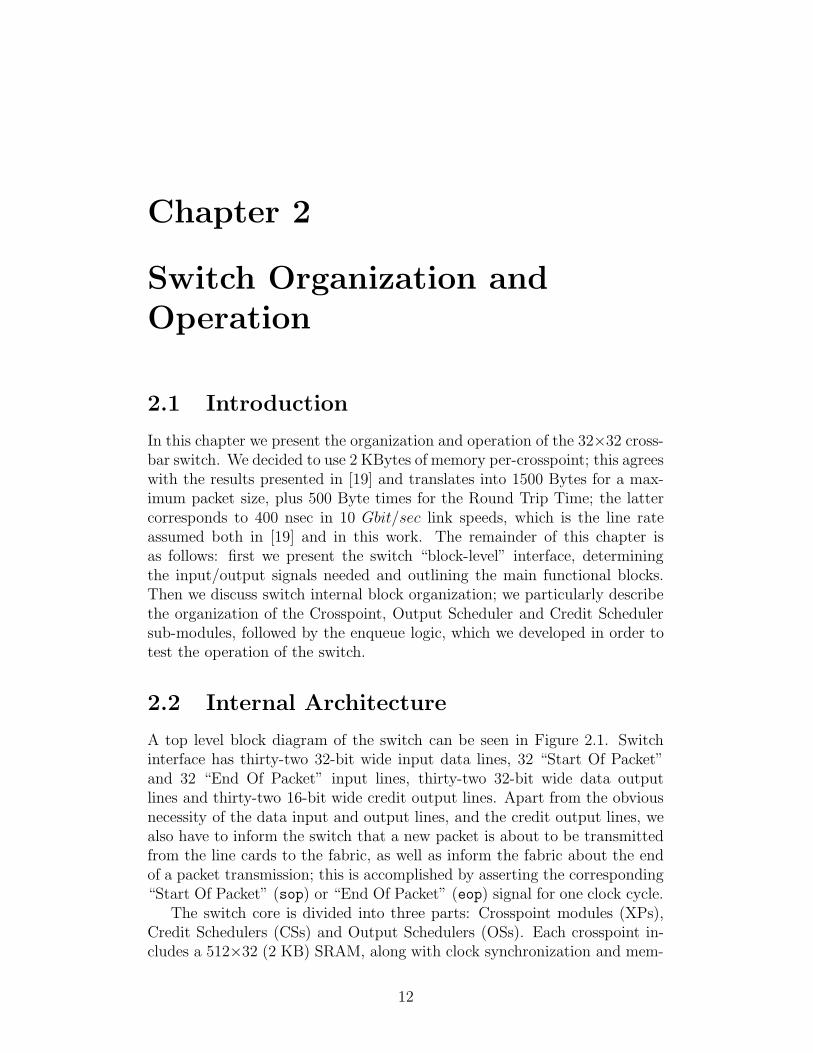
In this chapter we present the organization and operation of the 32×32 cross-bar switch. We decided to use 2 KBytes of memory per-crosspoint; this agreeswith the results presented in [19] and translates into 1500 Bytes for a max-imum packet size, plus 500 Byte times for the Round Trip Time; the lattercorresponds to 400 nsec in 10 Gbit/sec link speeds, which is the line rateassumed both in [19] and in this work. The remainder of this chapter isas follows: first we present the switch “block-level” interface, determiningthe input/output signals needed and outlining the main functional blocks.Then we discuss switch internal block organization; we particularly describethe organization of the Crosspoint, Output Scheduler and Credit Schedulersub-modules, followed by the enqueue logic, which we developed in order totest the operation of the switch.
2.2 Internal Architecture
A top level block diagram of the switch can be seen in Figure 2.1. Switchinterface has thirty-two 32-bit wide input data lines, 32 “Start Of Packet”and 32 “End Of Packet” input lines, thirty-two 32-bit wide data outputlines and thirty-two 16-bit wide credit output lines. Apart from the obviousnecessity of the data input and output lines, and the credit output lines, wealso have to inform the switch that a new packet is about to be transmittedfrom the line cards to the fabric, as well as inform the fabric about the endof a packet transmission; this is accomplished by asserting the corresponding“Start Of Packet” (sop) or “End Of Packet” (eop) signal for one clock cycle.
The switch core is divided into three parts: Crosspoint modules (XPs),Credit Schedulers (CSs) and Output Schedulers (OSs). Each crosspoint in-cludes a 512×32 (2 KB) SRAM, along with clock synchronization and mem-
12

CHAPTER 2. SWITCH ORGANIZATION AND OPERATION 13
output 2
32XP XP XP XP
CRS
32
1,1XP XP XP XP
1,2 1,3 1,32
line in 1
1CRS
2,1 2,3
2
2,32
32XP XP XP XP
CRS32
32,1 32,2 32,3 32,32
OS 1
creditpulses
32
32
creditpulses
32
32
creditpulses
32
32
line out 1
creditpulses
32
32
XPoutputs outputs
XPoutputs
XPoutputs
XP32 3232 32
line out 2 line out 3
OS 2 OS 3 OS 32
line out 32
2,2
16credit
eopsop
sopeop
line in 2
credit
16output 32
LINE
LINE
CARD 1LINE
CARD 2
CARD 32
sopeop
line in 32
credit
16
output 1
Figure 2.1: 32×32 crossbar switch block diagram: the switch consists of 32 × 32 =1024 crosspoints, and 32 output and credit schedulers. Line card logic is locatedoutside the switch core.
ory enqueue/dequeue logic. A 32×32 switch needs 32×32=1024 XPs, thus 16Mbits of memory. Credit Schedulers contain mechanisms for collecting andsending credit information to the input line cards, whereas Output Sched-ulers are responsible for selecting eligible flows that can send their packetsto the chip outputs. Both the Credit and Output Schedulers implementthe plain Round Robin discipline. Other scheduling disciplines, being fairer,could also be supported (i.e. [34]).
We place the clock domain boundaries in the crosspoint modules; thus,elastic buffers at the chip inputs are eliminated, which reduces latency andpower consumption, as each word of packet payload is only written once intoand read once out of a memory during its transition through the chip [19].Note that the only control information that has to traverse two differentclock domains in the switch organization presented, is the “new packet”arrival notification pulse. What is more, the two clock domains must operate

CHAPTER 2. SWITCH ORGANIZATION AND OPERATION 14
in almost the same frequency, as the input and output links have the samespeed. These observations significantly simplify crossbar design, as such 1-bitsynchronization circuits are very simple and efficient.
Before explaining the three main switch components in more detail, itshould be noted that the switch supports directly TCP/IP packets, of sizes40-1500 Bytes. Packet size must be a multiple of 4 and, if this is not thecase, the input line cards have to fill the remaining bytes of the last wordand accordingly increase the size of the packet. The only other informationneeded for the switch to operate is an output destination 32-bit multicast bit-mask, which is sent just before the actual packet; this information is paddedby the line card logic and the positions of the “1” indicate the crosspoints inwhich the packet is destined to or, equivalently, the outputs that the packetmust be sent to. Destination bit-mask and packet size are accompanied bya “time of transmission” value and a “packet serial number” in the payload,both of which were added for debugging and statistic purposes (see Figure2.2).
0
destinationbit−mask transmission
time of
31 0 31 0 31size
packetserial number
packet packetdata
31016
packet payload
Figure 2.2: Supported packet format: apart from packet size (16 bits), atime of transmission (32 bits) and a packet serial number (32 bits) value waspadded for statistic and debugging purposes. Packet payload follows. Noticethe 32-bit mask added at the begining of the packet.
2.2.1 Crosspoint Blocks (Crosspoints)
Crosspoints (XPs) are responsible for storing/retrieving packets into/fromtheir corresponding buffer memories. Figure 2.3 shows the top-level blockdiagram of the crosspoint: a 32-bit wide packet data bus enters each cross-point, along with the sop and eop signals. Each crosspoint receives a deq
signal from the corresponding column output scheduler and sends to theoutput a 32-bit data_out value. Notice the two different clock domains:the clock domain controlled by clk_wr contains the writing circuits, whileclk_rd handles the data reads.
Crosspoint organization is shown in Figure 2.4. Each XP has a 32-bitwide input datapath, along with two control signals: a “Start Of Packet”(sop) signal, which must be asserted for one clock cycle during the trans-mission of the first packet word and an “End Of Packet” (eop) signal, whichis asserted during the transmission of the last packet words. The sop signalinforms XP logic that a new packet is being sent. Each crosspoint looks indi-vidually at a 32-bit destination bit-mask, described in the previous section,

CHAPTER 2. SWITCH ORGANIZATION AND OPERATION 15
reset
CROSSPOINTsop
eop
line in data out
deq
3232
clk_wr clk_rd
Figure 2.3: Crosspoint block diagram.
and accordingly decides if the certain packet should be handled by it or not.The eop signal informs the crosspoint logic that the data enqueueing muststop.
to next
synchronized
wrData
wrAddr
enqueue
32
32
32
one−bitsynchronizer
my_pck data outdeq
data in
eop
sop
RS
my_pckXP
MEM
9
dequeue
9
write clockdomain
read clockdomain
to column output scheduler
wr_en rd_en
rdAddr
rdData
"column" XP
Figure 2.4: Crosspoint organization: notice the two clock domains; they meetin the memory and in the 1-bit synchronizer circuit.
Both sop and eop signals are needed in order to reduce the complexity ofthe switch core. In fact, in order to remove those 64 signals, we would haveto include some line-card and the packet enqueue control logic inside theswitch, which would add to its area and complexity. On the other hand, ifthose logic blocks were placed inside the switch, credits would not have to be

CHAPTER 2. SWITCH ORGANIZATION AND OPERATION 16
sent to the line cards, which would decrease the number of I/O ports needed.Although the last argument is very important in the case of medium- tolarge-scale buffered crossbars (as chip I/O throughput is limited and has toremain low for pin count, power consumption, and pricing reasons), a cleverorganization of credit logic can remove this initially predicted overhead 1.
In particular, in order to remove the eop signal, extra logic would haveto be added inside the switch, which would detect the sop arrival, sendthe enqueue signal to the corresponding crosspoint, capture and decrementthe packet’s size, and deassert the enqueue signal when the packet is written.During most of the stages of this work, this logic was actually included in theswitch, but its necessity proved worthless, as with just a little I/O throughputoverhead 2, this logic was easily omitted from the fabric. Note that only 32such “enqueue logic” blocks were used, as we only needed one per switchrow: every crosspoint that actually enqueued a packet would “listen” to theeop signal generated by that logic; the rest would just ignore it.
When both sop and the corresponding bit of the bit-mask are asserted,the crosspoint logic must perform a packet enqueue to the SRAM. This iscarried out by setting a latched signal, called my_pck, which in turn assertsthe SRAM’s write enable and increments the 9-bit enqueue address counter.When eop signal arrives, the enqueue FSM deasserts write enable and stopsthe enqueue pointer from incrementing.
We must also forward the my_pck signal to the corresponding outputscheduler, informing that a packet is being enqueued to one of the 32 cross-points connected to the column’s scheduler. This event wakes up the outputscheduler if the output link has been idle. We thus feed this new-packet-arrival signal to a simple 1-bit synchronizer, which is depicted in Figure 2.5.The signal sets an RS flip-flop and its output Q is sampled by a series ofthree D flip-flops clocked by the output clock domain (clk_rd). When thepulse is received, an acknowledgment signal travels back, which resets the RSflip-flop. The synchronization delay is 5 clock cycles, far less than the min-imum packet size (40 Bytes) enqueue time, which, in the case of our 32-bitdatapath, corresponds to 10 cycles. Note that the two clock frequencies arealways close to each other, which is always the case in switches, since theyhave the same input and output throughput. Synchronizer design is brieflypresented in the Appendix.
Packets are enqueued/dequeued in a 512×32 (2 KByte) Two-Port Reg-ister File SRAM from Virtual Silicon Technology [43]. This memory hasa 32-bit port for read and an independent 32-bit port for write; read andwrite addresses are 9 bits wide (see Figure 2.3). The independent read andwrite cycles are timed with respect to their own clocks, namely clk_rd andclk_wr respectively. It should be noted that during a read cycle, the output
1This organization is thoroughly presented in a following section.2Not high chip I/O overhead, though, as “End Of Packet” transmission is carried out
at most every “minimum-packet-size” time, which is 10 clock cycles in our 32-bit datapath;hence fast and expensive tranceivers are not needed.

CHAPTER 2. SWITCH ORGANIZATION AND OPERATION 17
clk_in
my_pck
synchronizedmy_pck
clk out
bit_d0 bit_d1 bit_det
positive edge detector
bit_d2 bit_d3
ack signal
RS Flip−Flop
Figure 2.5: 1-bit synchronizer circuit.
bus values are held if read enable is not asserted. This read enable feature isused to save RAM power without the need for external clock gating.
The last part of the crosspoint logic is the dequeue sub-module. Wheneverthe output scheduler decides to dequeue a packet from the specific crosspoint,it asserts the deq signal, which fires the dequeue FSM corresponding to thatoutput; read enable is asserted and dequeue pointer is then incremented. Thedeq signal remains asserted for the time needed to fully dequeue the packet,and is controlled by the output scheduler dequeue logic.
2.2.2 Output Schedulers
The output schedulers are responsible for: (a) selecting the next eligible flowfrom a certain crosspoint of the same column; (b) initializing the transmissionof packets to the specific switch output; and (c) sending a credit back to theline cards. A flow is called eligible if the corresponding crosspoint containspackets that are waiting to be sent. If there are more than one eligible flows,the output scheduler has to select one of them; this selection can dependon the flow priority (possibly its weight - i.e. in Weighted Round Robinscheduling), or on a plain round robin policy. In this work we did not aimat implementing new and sophisticated output scheduler policies, but ratheruse a plain round robin scheduler: the output scheduler maintains a list ofthe eligible flows and after serving one flow, it selects the next eligible flowof the list 3. The output scheduler knows which flows are eligible or notthrough the synchronized my_pck signals it receives from the crosspoints ofthe same column. Since the synchronization delay is 5 clock cycles and apacket transmission lasts for 10 cycles, we claim that the scheduler supportscut-through operation (with a 5 cycle overhead): when all 32 crosspoints
3In the first stages of this thesis, we developed a Weighted Round Robin output sched-uler with “smart comparator usage” for a 4×4 crossbar switch, that would be implementedin an FPGA. This scheduler is examined in the Appendix.

CHAPTER 2. SWITCH ORGANIZATION AND OPERATION 18
of a column are empty and a minimum-size packet arrives to one of them,only 5 clock cycles are needed to initialize its dequeue to the switch output,whereas the time needed for the packet to be written to the crosspoint is 10clock cycles.
Output scheduler block diagram can be seen in Figure 2.6, while its orga-nization is presented in Figure 2.7. The scheduler has thirty-two 32-bit data
deq
32
32line out 1
32
32
32
line out 2
line out 3
line out 4
line out 32
data out32OUTPUT
SCHEDULER
clk_rdreset
3232 32
my_pcksynchronized credit
signals
Figure 2.6: RR Output Scheduler block diagram.
inputs, which originate from the column crosspoint memories’ data outputs.32 synchronized my_pck signals are also sent from the crosspoint synchroniza-tion logic. The output scheduler sends 32 credit signals back to the switchinputs and a 32-bit deq bus to the column crosspoints. The dequeue signalsact as read enable for the crosspoint memories.
In order to produce the list of eligible flows, the scheduler maintainsthirty-two 6-bit packet counters 4, which are incremented each time a syn-chronized my_pck signal arrives and decremented when the selected packet isbeing dequeued; when these counters are equal to zero, the flow is ineligible.The 32-bit eligibility mask that is created in this way enters a Round-RobinPriority Enforcer, which is responsible for selecting the next eligible flow (itsoutput is a 32-bit value, with one bit equal to “1” and 31 bits equal to zero).This 32-bit crosspoint selection bus is sent to the column crosspoints and atthe same time the specific packet counter value is decremented. When thefirst packet word is dequeued from the crosspoint and arrives at the sched-uler, the packet size is stored, in order to allow the scheduler to know whenit should stop dequeueing. If, while one packet has been almost dequeued,there exists at least one eligible flow in the same column, the scheduler hasto start pre-scheduling, in order to choose the next eligible flow and not missany clock cycles in between. Hence, back-to-back operation is achieved.
4Six bits are sufficient because each crosspoint buffer can store at most 50 (minimum-size) packets.

CHAPTER 2. SWITCH ORGANIZATION AND OPERATION 19
data out
signalsdeq
eligibility 6−bitpacket counters
RoundRobinPr. Enf.
32
eligibilitymask
XP 1,x
XP 2,x
XP 3,x
XP 32,x
outputMUX
32
32
32 deq
deq
deq
deq data out
data out
data out
pck_fin
flow_sel
data out(to switch output)
pck sizecounter
+/−
+/−
+/−
+/−
+/−
32
(from crosspoint column)synchronized
my_pck(outside output scheduler)(to credit schedulers)
credit signals crosspoint column
Figure 2.7: RR Output Scheduler organization: crosspoint memories are illustratedfor clarity; they do not belong to the output scheduler.
2.2.3 Credit Schedulers
Credit schedulers are responsible for: (a) collecting the credit signals fromthe output schedulers; and (b) sending them back to the line cards; there isone line card per row. Since it is the line cards’ responsibility to recover thereceiving clock (as happens with outgoing packet data), credits are sent inrespect to the output clock, hence no synchronization circuitry is required.
The credit format should satisfy one constraint: it should contain theabsolutely necessary information that the line card should know, in orderto save I/O bandwidth (package pins and expensive I/O pads). In order toremove as much logic possible from the switch core, we decided that the linecards should perform all necessary credit computing operations. For errorresilience purposes, the credit schedulers adopt a QFC-like [30] approach:instead of sending the information that “the next packet has just left fromcrosspoint . . . ” 5, they just send “the total, cumulative number of packetsthat have left up to now from crosspoint . . . , modulo 2k, is equal to . . . ” [19].As a result: (i) we do not need to send one credit for every packet; and (ii)even if some credits get lost, the next arriving credit carries cumulative in-formation from past ones, too 6. Line card logic is responsible for concluding
5This information could have the form of a 5-bit encoded crosspoint (i.e. output)number, but one such credit loss would have undesirable effects.
6We just have to ensure that at least one credit will safely arrive for every 2k departing

CHAPTER 2. SWITCH ORGANIZATION AND OPERATION 20
that the credit number just received is different from the previously storedcorresponding value, hence a new credit has arrived. Credit format is shownin figure 2.8. It is 16 bits wide, with the most significant 7 bits reserved forfuture use (possibly 2 bits for error checking purposes, plus 3 bits for sup-porting up to 8 distinct priorities). The next 4 bits contain the actual creditvalue (number of packets sent from the corresponding crosspoint), while the5 least significant bits refer to the crosspoint’s ID.
4
������������������������������������
������������������������������������
���������������
���������������
������������������������������������
������������������������������������
���������������
�����
��������
��������
�����������������������������������
�����������������������������������015
valuecredit counter crosspoint ID
2 error checking bits)RFU (possibly 3 priority &
8
Figure 2.8: Credit format.
Figure 2.9 shows the credit scheduler block diagram. Each credit sched-uler module receives a 32-bit credit mask, referring to dequeues from thecorrespoinding row crosspoints, and sends a 16-bit credit bus to the respec-tive line card logic.
32
SCHEDULER
CREDIT
reset
creditout credit pulse
clk_rd
16
Figure 2.9: RR Credit Scheduler block diagram.
Credit scheduler internal organization is shown in Figure 2.10. The sched-uler maintains 32 4-bit “sent-packet” counters, which contain the number ofpackets that have been dequeued from the respective row crosspoints. Ob-viously this counter wraps around when 16 packets have been dequeued andthe 17-nth credit has just arrived.
Each time a credit arrives, the respective credit counter sets its outputcredit_change bit, informing the scheduler that its value has just changed.The 32-bit credit_change_mask value is connected to a Round Robin Prior-ity Enforcer, which selects the next (changed) credit value that will be sent tothe line cards. This is indicated by its 32-bit output, credit_choose_mask,which, except for selecting the credit value that will be sent to the line cards,is also responsible for resetting the credit_change flag of the correspondingcounter.
packets, i.e. before the counter wraps around.

CHAPTER 2. SWITCH ORGANIZATION AND OPERATION 21
ID
RobinRound
Pr. Enf.
32
credit
maskchange
5
RFU32
16
valuescountercredit
32
32
32 to 5ENC
creditoutput
(to switch output)
credit_choose_mask
credit_pulse_mask(from crosspoint row)
+
+
+
+
4−bit pack counters
4
4
7
5
row crosspoint
Figure 2.10: RR Credit Scheduler organization.
Assuming that credit switch outputs will use about 1/8 of the bandwidthof every switch packet data input/output 7, each 16-bit credit value will need4 clock cycles in order to be sent to the line card 8. As a result, scheduling iscarried out in 4-cycle intervals. Since scheduling time is 4 clock cycles, thescheduler needs 4 × 32 = 128 clock cycles to send all 32 credit values.
Credit signals can arrive at any time from the output schedulers, withthe extreme of all 32 bits of the credit_pulse_mask being set in one clockcycle. In this case, credit_change_mask is all “1” and one credit countervalue is selected to be sent. Due to the fact that the next credit signalswill come at least one minimum-packet transmission time after this event(10 clock cycles), no counter can overflow sooner than 170 clock cycles havepassed; hence, the scheduler has enough time to send all 32 credits beforeany counter wraps around.
Last of all, it should be noted that if the credit_change_mask is allzeroes, meaning that no credit has been received for at least the last 128clock cycles (nearly 13 packet-times), the credit scheduler sends the storedcredit counter values. In this way, the line card logic can check if the credit
7This is desirable in order to save package pins and I/O tranceiver pads.8In one cycle, 32 packet data bits are received/sent, hence if credits use 1/8 of this
bandwidth (4 bits per cycle), 4 cycles are needed for the transmission of the 16-bit creditvalue.

CHAPTER 2. SWITCH ORGANIZATION AND OPERATION 22
value has changed since last time and thus perform error checking.
2.2.4 Line Card Logic
The switch presented sofar could be tested in two ways: (a) by feeding thesimulator with trace files containing real or generated traffic; and/or (b) bydesigning a simple line card and feeding the switch with traffic from the linecard’s traffic generator. During the initial stages of the switch design, weused traces generated from the simulator which was written in C++ and isthoroughly presented in [29] and [19]. The trace files consisted of packet sizesand the exact time they were arriving at the switch inputs. Later on, thecredit logic designed in the simulator changed from the one we used and, as aresult, in order to test and verify the switch operation, we designed a Verilogmodel of the line card.
Line card block diagram is presented in Figure 2.11. Each line card is
to switch row
32
16
resetclk_wr
LINE
CARD
LOGICeop
sop
line out
credit in (from switch cr. output)
Figure 2.11: Line Card block diagram
responsible for sending packet data (32-bit line out bus), and the “Start OfPacket” (sop) and “End Of Packet” (eop) signals to the respective switchrow. Feedback information from the switch is packed in the 16-bit creditbus that is sent through the corresponding switch credit scheduler to theline card block. Line card constists of two parts: (a) packet constructionand transmission logic; and (b) credit processing logic. These two parts arecompletely independent, as a credit can come at any time, regardless of thestate of a possible packet transmission. The two parts are discussed in moredetail in the next two subsections.
Packet Construction and Transmission Logic
As each line card has multiple (32) Virtual Output Queues (VOQs), 32 FIFOqueues are maintained; these contain the size of each packet that has justbegun transmission from the line card to the switch. A 32-entry “emptycrosspoint buffer size” array is also used, in order to store the empty spaceof each crosspoint buffer of the corresponding switch row. The packet trans-mission FSM is shown in Figure 2.12. This FSM is in the IDLE state if nopacket can/has to be constructed and sent. When the enq signal is set, the

CHAPTER 2. SWITCH ORGANIZATION AND OPERATION 23
!pck_fin &
XMIT
IDLEPREPVOQ
XMITBM
PLXMIT
TS
PCK SNXMIT
enq
!pck_fits
pck_fin &!pre_schedule
!pck_fin &!pre_schedule
pck_fits
pre_schedule
Figure 2.12: Line card packet transmission FSM.
FSM goes to VOQ_PREP state. If the new packet’s size fits into the corre-sponding crosspoint buffer, pck_fits is asserted, packet size is enqueued inthe respective FIFO, the specific crosspoint buffer size is decremented bythe pck_sz value and the corresponding packet counter is incremented. Thenext four states are responsible for sending to the switch the packet bit mask(XMIT_BM), packet length (XMIT_PL), a timestamp (XMIT_TS) and the packet’sserial number (XMIT_PCK_SN); packet format is shown in section 2.2. In orderto support back-to-back transmission (pre_schedule is asserted), the FSMgoes to the VOQ_PREP state before the packet’s last word is sent to the switch,and the preperations for a new packet transmission start.
Credit Processing Logic
In this behavioral module, a 32-entry credit array is maintained in order tostore the previous credit counter values. These values are compared withthe newly received ones: if they differ, then we have a new credit for thatparticular VOQ. As a result, a FIFO dequeue has to be performed, the newcredit value must be stored and the empty space of that particular crosspointhas to be incremented by the packet size stored in the head of the FIFO.
Switch Verification
The switch is tested by using the Cadence [20] NCLaunch tool. Three typesof traffic are sent: (a) all minimum-size packets (40 Bytes); (b) randomlyselected packets; and (c) only maximum-size packets (1500 Bytes). Packetsare sent either back-to-back, or with a random interpacket delay. We usetwo test scenarios: (a) all inputs send packets to all outputs randomly; (b)all inputs send packets to a specific output; obviously, the scenario that puts

CHAPTER 2. SWITCH ORGANIZATION AND OPERATION 24
more stress on the switch core is when smallest size packets are sent back-to-back to a specific output. In that case, the crosspoint buffers of thatswitch “column” are filled with 40-Byte packets and the output schedulerhas to make a decision in 10 clock cycles, which is the transmission time ofa minimum-size packet. In this way, we achieve back-to-back operation.
2.3 Conclusions
In this chapter we presented in detail the switch and line card internal orga-nization and operation. Crosspoint logic should be as small as possible, asthe O(N2) crossbar complexity could prove, in the later design stages (syn-thesis and placement & routing), to be a prohibitive implementation factor.By minimizing the logic at the clock domain boundaries, synchronization be-comes easy and simple. Furthermore, no packet segmentation and reassemblyis required, by directly supporting variable-size operation and with paddinga 32-bit destination bit-mask at the beginning of each packet header. Outputand credit schedulers are as simple as possible, whereas their aggregate sizeis orders of magnitude smaller than total memory area; hence, more complexpolicies can also be supported, without significantly affecting the total switchcore area.

Chapter 3
Logic Synthesis
3.1 Introduction
Logic synthesis is one of the most important phases of the design flow in state-of-the-art circuits. It aims at transforming the HDL (usually Verilog HDLor VHDL) description of the circuit into a technology-dependent, Gate-Levelnetlist. Through this process, the hardware designer defines the environ-mental conditions, contraints, compile methodology, design rules and targetlibraries, in order to achieve certain design goals set by the initial specifica-tions. The Gate-Level representation of the circuit is the input file to thePlace & Route tool, which is described in the next chapter.
The tool we use for the logic synthesis of the switch is Synopsys DesignCompiler (DC) [46], the most widely used synthesis tool. Design Compileroptimizes logic designs for speed, area and wire routability. From the definedgoals, DC synthesizes the circuit and tailors it to a target technology. Therest of this chapter is as follows: first we present the two ways the synthesisprocedure can be carried out, flat and hierarchical, and compare them. Wethen describe the synthesis flow we followed for the 32×32 buffered crossbarswitch, accompanied by our synthesis results. Later on, we will comparethese results to the placement & routing ones and useful conclusions will bedrawn. Finally, we briefly talk about post-synthesis verification.
3.2 Synthesis Flow
The synthesis flow that we follow can be seen in Figure 3.1. We initiallyread the design under synthesis; this enables DC to load all design instancesinto memory and report possible HDL errors. Next we set initial designconstraints, such as: (a) maximum circuit area, or zero if ultra “size” mini-mization has to be performed; (b) circuit clock(s); (c) maximum transitiontime of specific nets; (d) maximum capacitance of nets, etc. Circuit areaand clock cycle specification are usually enough in order to synthesize mostcircuits. Design must then be checked. This enables Synopsys to report mis-
25

CHAPTER 3. LOGIC SYNTHESIS 26
takes which usually have to do with wrong module instantiations, or interfacemismatches. After this “check design” phase is complete, we optimize thedesign, by setting again the appropriate values for the different constraints.Usually, we wish to minimize circuit area and increase operating frequency.Some nets may also have to be constrained in terms of capacitance or tim-ing, but these decisions can usually only be taken into account after actualchip layout is defined. As a result, the latter has to be almost defined be-fore synthesis commences. After this final phase, we analyse the reports ofthe tool and check for unmet constraints. If such exist, the designer usuallyhas to: (a) rewrite HDL code, in order, for example, to meet certain tim-ing constraints; (b) modify the constraints themselves, which unfortunatelymay result in a slightly different design; (c) change compile attributes, forexample, change tool optimization priorities; (d) ungroup (i.e. remove anyhierarchy from design blocks), in order to offer the tool the ability to handlelarger modules and possibly produce better analysis and optimization results;unfortunately, we cannot completely remove the hierarchy in the case of verylarge designs. Last of all, we can analyze power consumption and performpower optimizations. Synthesis power estimation is presented in chapter 5,while power optimization techniques can be found in the Appendix.
3.3 Flat vs. Hierarchical Synthesis
Flat designs contain no subdesigns and have only one structural level; theyonly contain library cells. Design Compiler does not optimize across hi-erarchical boundaries; therefore, by removing the hierarchy within certaindesigns, timing results can be improved. Removing of hierarchy is calledungrouping. Through this task, subdesigns of a given level of hierarchy aremerged into the parent design.
Although flat synthesis usually provides the best results, this approachcannot be followed in the case of large designs. This is because, at the pres-ence of a large number of multi-instantiated modules, ungrouping will buildevery instantiated module from scratch, thus needing large computationalresources. In such cases, a hierarchical approach is proposed: each moduleis synthesized, fully optimized, and saved as a separate design. Then, it isloaded back to the tool and linked into the higher hierarchy module. Synop-sys will then only have to deal with identicaly-synthesized module instantia-tions, which will reduce execution time. One disadvantage of the hierarchicalapproach is that the tool cannot perform low-level optimizations, after thehigher-level design is synthesized. Such optimizations are useful when, forexample, the designer wishes to optimize the design for power consumption.In that case, cells that are located at non-critical paths are usually replacedby others that are smaller, hence consume less power, but are slower. Suchoptimizations cannot be performed inside low-hierarchy blocks directly atthe top-level of a hierarchical design.

CHAPTER 3. LOGIC SYNTHESIS 27
Check
DesignRead in
timing goalsand realisticSet attributes
Errors
Optimize
resultsGood
Done
Fixerrors
Rewrite HDL code,Change constraints,
Ungroup design blocksModify compile attributes,
Start
design
Figure 3.1: Generic synthesis flow.
Synthesis hierarchy organization followed can be seen in Figure 3.2. Wesynthesize low hierarchy blocks, like crosspoints, output and credit schedulersin a flat manner. This is decided in order to achieve maximum optimizationon those blocks; the latter is required because, due to the large instantiationnumber of these blocks (1024 crosspoint and 32 output and credit sched-uler modules), lack of optimization can eventually limit the design goals.These low hierarchy blocks are then grouped into higher hierarchy modules:32 columns include 32 crosspoints and one output scheduler module each,whereas one credit module is used to group the 32 credit schedulers. Thesegroupings are performed in the RTL, but can also be carried out success-fully through the Synopsys environment, by using the group command. Asa result, the top design module consists of merely 32 column and one creditmodule.
It should be noted that during the Placement and Routing (P&R) designstage, we observed that the tool could not successfully perform P&R of these

CHAPTER 3. LOGIC SYNTHESIS 28
Module
BufferedCrossbar Top
Module
Approach (link)
Approach
Hierarchical
(ungroup)
Flat
BufferedCrossbar Top
Module
CrosspointColumn
flatCSXP
flat
OS flat
CreditHier.
module
32 crosspoints
32 crosspointcolumns
32 creditschedulers
Alternative (Final)HierarchyApproach (group)
16 ColumnModule
16 Column
Figure 3.2: Synthesis hierarchy organization: crosspoint modules (XP), out-put schedulers (OS) and credit schedulers (CS) were synthesized in a flatmanner. Each crossbar column was synthesized by linking 32 cosspoints andone output scheduler module. The 32 credit scheduler modules were linkedinto a higher hierarchy module, as well. The 32 crosspoint columns and thecredit module were linked into the top hierarchy module. Later on, it wasrealized that placement and routing would be performed easier if we addedanother level of hierarchy, by grouping the 32 columns into two sets of 16;this procedure required circuit resynthesis and is illustrated on the left sideof the figure.
33 modules; this was mainly due to the large size of files handled by the tool.As a result, we decided to go back to the synthesis stage and regroup the 32columns into 2 sets of 16; P&R would therefore be performed hierarchicallyinto these 2 modules, which would connect to the credit block in the top-level. This grouping was carried out through the Synopsys environment, byusing the group command.
3.4 Synthesis Results
The synthesis process is completed relatively easily and timing contraintsare met, while circuit area is kept to a minimum. Timing constraints are ofthe greatest importance, as we opted for a clock frequency of 300 MHz (3.35nsec clock cycle); we were constrained to 300 MHz due to the fact that it was
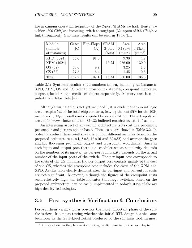
CHAPTER 3. LOGIC SYNTHESIS 29
the maximum operating frequency of the 2-port SRAMs we had. Hence, weachieve 300 Gbit/sec incoming switch throughput (32 inputs of 9.6 Gbit/seclink throughput). Synthesis results can be seen in Table 3.1.
Module Gates Flip-Flops SRAM Area Area(number (K) (K) 2-port 0.18µm 0.13µmof instances) (bits) (mm2) (mm2)
XPD (1024) 65.0 91.0 9.30 4.2XPM (1024) 16 M 286.00 130.0OS (32) 68.0 9.7 3.25 1.5CS (32) 27.5 6.4 1.45 0.6
Total 162.7 107.1 16 M 300.00 136.3
Table 3.1: Synthesis results: total numbers shown, including all instances.XPD, XPM, OS and CS refer to crosspoint datapath, crosspoint memories,output schedulers and credit schedulers respectively. Memory area is com-puted from datasheets [43].
Although wiring area is not yet included 1, it is evident that circuit logicarea occupies 5% of the total chip core area, leaving the rest 95% for the 1024memories. 0.13µm results are computed by extrapolation. The extrapolatedarea of 140mm2 shows that the 32×32 buffered crossbar switch is feasible.
An interesting aspect of any switch architecture is its cost in a per-input,per-output and per-crosspoint basis. Those costs are shown in Table 3.2. Inorder to produce these results, we design four different switches based on theproposed architecture (4×4, 8×8, 16×16 and 32×32) and average the gateand flip flop sums per input, output and crosspoint, accordingly. Since ineach input and output port there is a scheduler whose complexity dependson the numbers of its inputs, the per-port complexity depends on the actualnumber of the input ports of the switch. The per-input cost corresponds tothe costs of the CS modules, the per-output cost consists mainly of the costof the OS, whereas the crosspoint cost includes the costs of the XPM andXPD. As this table clearly demonstrates, the per-input and per-output costsare not significant. Moreover, although the figures of the crosspoint costsseem relatively high, the table indicates that large switches, based on theproposed architecture, can be easily implemented in today’s state-of-the arthigh density technologies.
3.5 Post-synthesis Verification & Conclusions
Post-synthesis verification is possibly the most important phase of the syn-thesis flow. It aims at testing whether the initial RTL design has the samebehaviour as the Gate-Level netlist produced by the synthesis tool. In most
1But is included in the placement & routing results presented in the next chapter.

CHAPTER 3. LOGIC SYNTHESIS 30
Gates FFper-input 27 x i 2.5 x iper-output 70 x i 10 x iper-crosspoint 63 70
Table 3.2: Per input/output/crosspoint logic costs; i in the number of theinput ports of the switch.
of the cases the initial results are not the same, and the designer has to care-fully investigate the reason for the erroneous behaviour of the Gate-Levelnetlist. Usual mistakes happen when the circuit does not reset correctly, amistake that can pass unseen from the HDL compiler & simulator, but, ofcourse, the actual circuit will not work correctly.
Our synthesized Gate-Level netlist is imported back to the Verilog com-piler (Cadence NCLaunch [20]) and is tested within the same environmentas the initial RTL design. The final netlist proves to behave correctly. Thenetlist is now ready to be imported to the Place & Route tool for the finalphase of the design process.

Chapter 4
Placement and Routing
In this chapter we explore the Placement and Routing (P&R) process fol-lowed when implementing the 32×32 buffered crossbar switch examined inthe previous chapters. This process was a major part of this thesis, both intime and effort terms. Although the chip is “regular”, as shown in the nextsection, it proves too large for the available P&R tool to handle in a flatmanner; as a result, we have to resort in a hierarchical P&R process, whichposes many difficulties, in terms of choosing the optimal hierarchy organiza-tion that will reduce interface cost and result in a regular final chip aspectratio. The rest of this chapter is as follows: at first we compare flat versushierarchical P&R and present the exact flow followed in our case. Next, weexamine the various hierarchy organizations proposed during the P&R pro-cess and propose our final organization, followed by a thorough presentationof the P&R process for the major hierarchy components of the switch. Lastof all, we present our post-P&R area and power consumption results.
4.1 Flat vs. Hierarchical Placement & Rout-
ing
The 32×32 crossbar chip is a highly regular chip, consisting merely of 32identical “rows” and 32 indentical “columns” (see Figure 2.1). P&R can betherefore be quite straightforward, in the presence of a tool destined for “handdesign”: the designer places each crosspoint at specific positions and wiresare routed through each row and column. Because such a tool does not exist,we have to use automatic P&R tools. It should be noted that automatic P&Rtools offer some freedom for user-defined logic cell/block placement, but sucha process is difficult when carried out for a large number of logic cells/blocks.Furthermore, the tools we can use have gate limitations in their automaticP&R algorithms, as a result we follow a hierarchical P&R approach. Last,the number and size of instances must also be taken into account, as thepresence of a large number of complicated instances (which means timingand layout file complexity) can pose great difficulties in the P&R process.
31
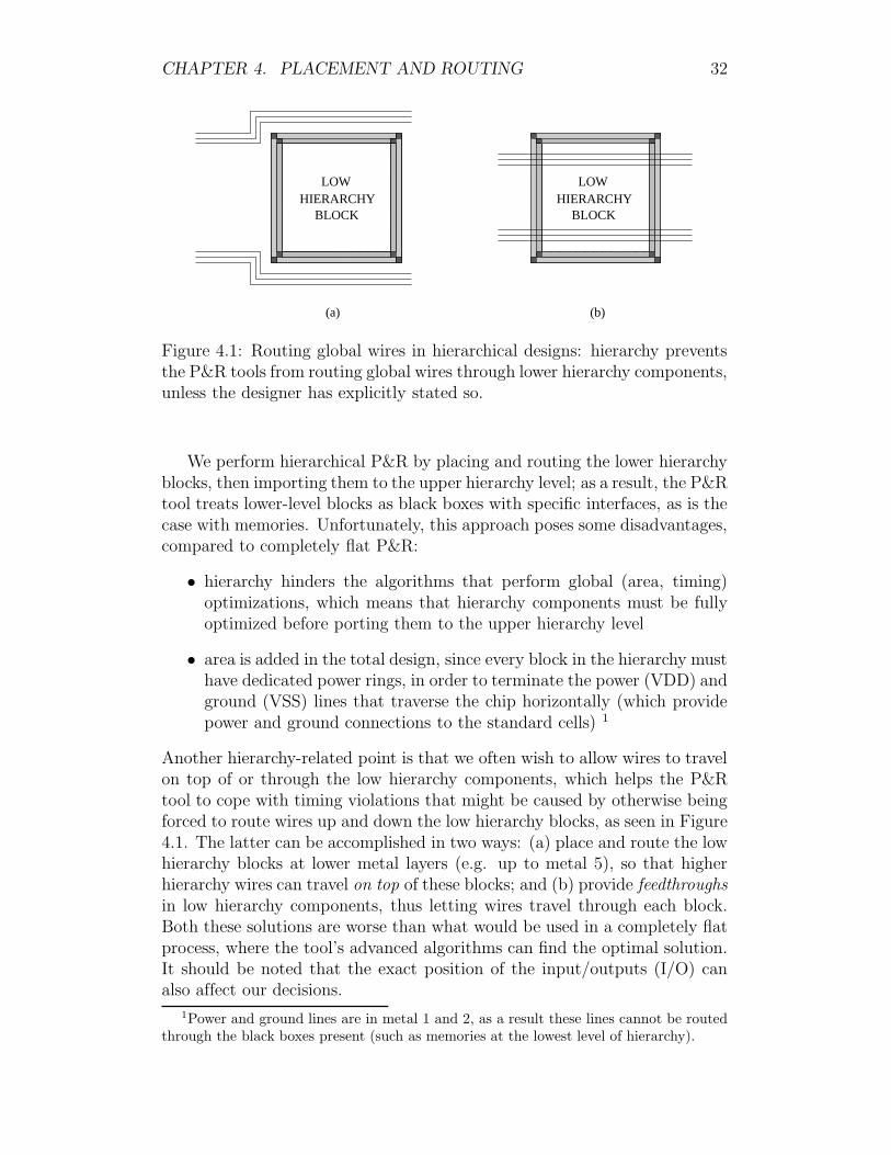
CHAPTER 4. PLACEMENT AND ROUTING 32
(b)
�������
�������
���������������������
���������������������������������
��������������������������
������������
��������������������������
�������
�������
�������
���������������������
���������������������
���������������������
�������������������������������������
������������������������������
������������������������������
���������������������������������������������������
���������������������
�������
BLOCK
LOWHIERARCHY
BLOCK
LOWHIERARCHY
(a)
Figure 4.1: Routing global wires in hierarchical designs: hierarchy preventsthe P&R tools from routing global wires through lower hierarchy components,unless the designer has explicitly stated so.
We perform hierarchical P&R by placing and routing the lower hierarchyblocks, then importing them to the upper hierarchy level; as a result, the P&Rtool treats lower-level blocks as black boxes with specific interfaces, as is thecase with memories. Unfortunately, this approach poses some disadvantages,compared to completely flat P&R:
• hierarchy hinders the algorithms that perform global (area, timing)optimizations, which means that hierarchy components must be fullyoptimized before porting them to the upper hierarchy level
• area is added in the total design, since every block in the hierarchy musthave dedicated power rings, in order to terminate the power (VDD) andground (VSS) lines that traverse the chip horizontally (which providepower and ground connections to the standard cells) 1
Another hierarchy-related point is that we often wish to allow wires to travelon top of or through the low hierarchy components, which helps the P&Rtool to cope with timing violations that might be caused by otherwise beingforced to route wires up and down the low hierarchy blocks, as seen in Figure4.1. The latter can be accomplished in two ways: (a) place and route the lowhierarchy blocks at lower metal layers (e.g. up to metal 5), so that higherhierarchy wires can travel on top of these blocks; and (b) provide feedthroughsin low hierarchy components, thus letting wires travel through each block.Both these solutions are worse than what would be used in a completely flatprocess, where the tool’s advanced algorithms can find the optimal solution.It should be noted that the exact position of the input/outputs (I/O) canalso affect our decisions.
1Power and ground lines are in metal 1 and 2, as a result these lines cannot be routedthrough the black boxes present (such as memories at the lowest level of hierarchy).

CHAPTER 4. PLACEMENT AND ROUTING 33
32 credit schedulers
OS
XP 1
XP 2
XP 3
XP 4
XP 5
XP 32
32
line in 132
32
32
32
32
32
32
line in 2
line in 3
line in 4
line in 5
eopsop
sopeop
eopsop
eopsop
eopsop
line in 32eopsop
32
32
32
32
32
32C
OL
UM
N 2
CO
LU
MN
3
CO
LU
MN
4
CO
LU
MN
32
16 16 16 16 16 16
credit pulses
32 32 3232
32 data outputs
32 credit outputs
32 li
ne in
puts
CRS 1 CRS 32CRS 4CRS 3CRS 2
Figure 4.2: Switch internal organization: block interfaces.
4.2 Choosing a Hierarchy Organization
As can be seen in Figure 4.2, each switch column has thirty-two 32-bit datainputs, 64 single bit sop and eop inputs, one 32-bit data output and thirty-two 16-bit credit outputs; these amount to 1088 inputs and 48 outputs. Fromthe figure it is evident that input lines have to connect to every switch column;as a result, in order to avoid long and unwanted data lines, we come up withthe two strategies mentioned in the previous section: (a) place and routeeach column up to a lower metal layer, so that data lines can travel overevery column; and (b) pass all data lines through every column from the RTLlevel, using dummy wires. We conclude that the latter solution is preferrable,because, as we are aiming at the smalest possible column area, solution (a)will most probably be not as “area-aware” as solution (b). This is because,if we follow solution (a), each column will be placed & routed up to metallayer 5, leaving the (highest) metal layer 6 unrouted by local column wires;hence, column area optimization will not be accomplished.
Another interesting point is memory orientation. As shown in Figure 4.4,memory interface lies on the three of the four sides of the memory, with datalines lying on the south side of its surface. This initially leads us to placeevery memory with its long side on the “x-axis”, which results in a fairly“low” and “wide” column (see Figure 4.3(a)).

CHAPTER 4. PLACEMENT AND ROUTING 34
(b)
13000 um 28000 um
line in line out
credits
FINAL CHIP ASPECT
data out
1100 um
FINAL CHIP ASPECT
400 um
data out
credits
line in line out
data out
credits
line outline in
900 um
FINAL CHIP ASPECTRATIO: 3.6 x 1.4 mm
(a) (c)
RATIO: 2.9 x 1.4 mm
13500 um
RATIO: 1.3 x 2.9 mm
Figure 4.3: Column orientation alternatives: Case (a) has the worst aspectratio, almost 1:3 and was thus abandoned. Case (b), although having betterand acceptable aspect ratio (1:2), was unroutable. Case (c) proved to beeasy to route, without making the aspect ratio any worse. Chip core aspectratios can be seen in the bottom of the figure.
As a result, data lines enter the column from the west sides (and exit fromthe opposite side), credit signals exit from the north side, leaving the southside for data outputs. Fortunately, the P&R tool we use, Cadence Encounter,offers the ability to manualy place hard blocks (memories) and even softblocks, like our designed modules, although not so exact, as is the case withhard blocks. Unfortunately, this organization leads to an aspect ratio of 1:3for the whole chip core, which is obviously not prefferable. By placing thememories with their “small” side on the x-axis (see Figure 4.3(b)), althoughresulting in an aspect ratio of 1:2, will also result in very long columns,which makes P&R difficult, if not impossible, as long wires have to traversethe whole column height; the tool will thus have to buffer strongly thesewires, which adds to the total column area and core power consumption.
On the other hand, the placement of Figure 4.3(c) seems to be the bestalternative present. In this organization, the 32 columns are divided in 2and placed with their “small” sides on the x-axis. As a result, total columnwidth is approximately 900 µm and the corresponding height 14000 µm,

CHAPTER 4. PLACEMENT AND ROUTING 35
in
dequeuepointer
11
335 um
880 um
11 enqueuepointer
32 32
dataout
data
Figure 4.4: Memory layout: all signals connect to the lower 1/3 of the mem-ory (noted with the dotted line). Memory is placed & routed up to metallayer 4.
which results in a 15000µm×29000µm switch core, with total area 420 mm2
and aspect ratio of 1:2.
4.3 Placement and Routing Flow
We place & route the switch chip core with Cadence Encounter [20]. P&Rflow followed can be seen in Figure 4.5. It comprises of various stages, some ofthem being optional, although important for new design cases; we present acomprehensive P&R tutorial in the Appendix. At first the design is importedto the tool. The files needed are technology dependent and are either given bythe technology vendor (in our case Virtual Silicon UMC 0.18µm [21]) or areproduced by the synthesis tool (in our case Synopsys Design Compiler). Thevendor provides the P&R tool with (a) technology library - .lib files, whichcontain the exact electrical characteristics of the library standard cells, (b)layout - .lef files, which include standard cell actual layout, pin placementand metal layer usage and (c) verilog - .v files, containing the interface ofevery standard cell. The same vendor also provides the memory models, sothe memory timing library - .tlf file was also included. From the synthesistool point of view, the only information needed to be passed on to the P&Rtool is the Synopsys technology mapped - .v Gate-Level representation of thedesign.
After importing the design, the designer has to Floorplan the variousverilog modules and/or black boxes in the actual chip. Modules can be either“softly” placed, that is the tool can alter their shape, or “hard” placed,in which case their shape cannot change significantly or at all during theplacement phase. Power rings are created and block rings are added forpower/ground termination purposes. Input/Output pins are also placed inthis stage: from the switch layout provided in Figure 4.2, it seems obvious to

CHAPTER 4. PLACEMENT AND ROUTING 36
No
Designplaceable?
NanoRoute)
placementHigh effort,timing driven
success?
Clock tree synthesis
routeable?Design
Medium effort trial route
Medium effort trial placement
−I/O placement−black box placement−row utilization
Floorplaning
−technology library files − .lib−layout files − .lef−timing library files − .tlf−standard cell HDL files − .v−design HDL gate level netlist files − .v
Design import
CTS
violations?Timing
Finish
High effort timing drivenrouting (WROUTE or
Yes
No
Yes
No
Yes
No
Yes
Figure 4.5: Placement and Routing Flow followed. Some stages (pad place-ment, crosstalk checks, DFT) were omitted, as we opted in demonstratingthe feasibility of the idea, not manufacture an actual chip.
place all input pins (data and sop / eop signals) on the west side of the chip,data output lines on the south side and credit outputs on the north side.Note that decisions carried out in this stage are of the greatest importance,
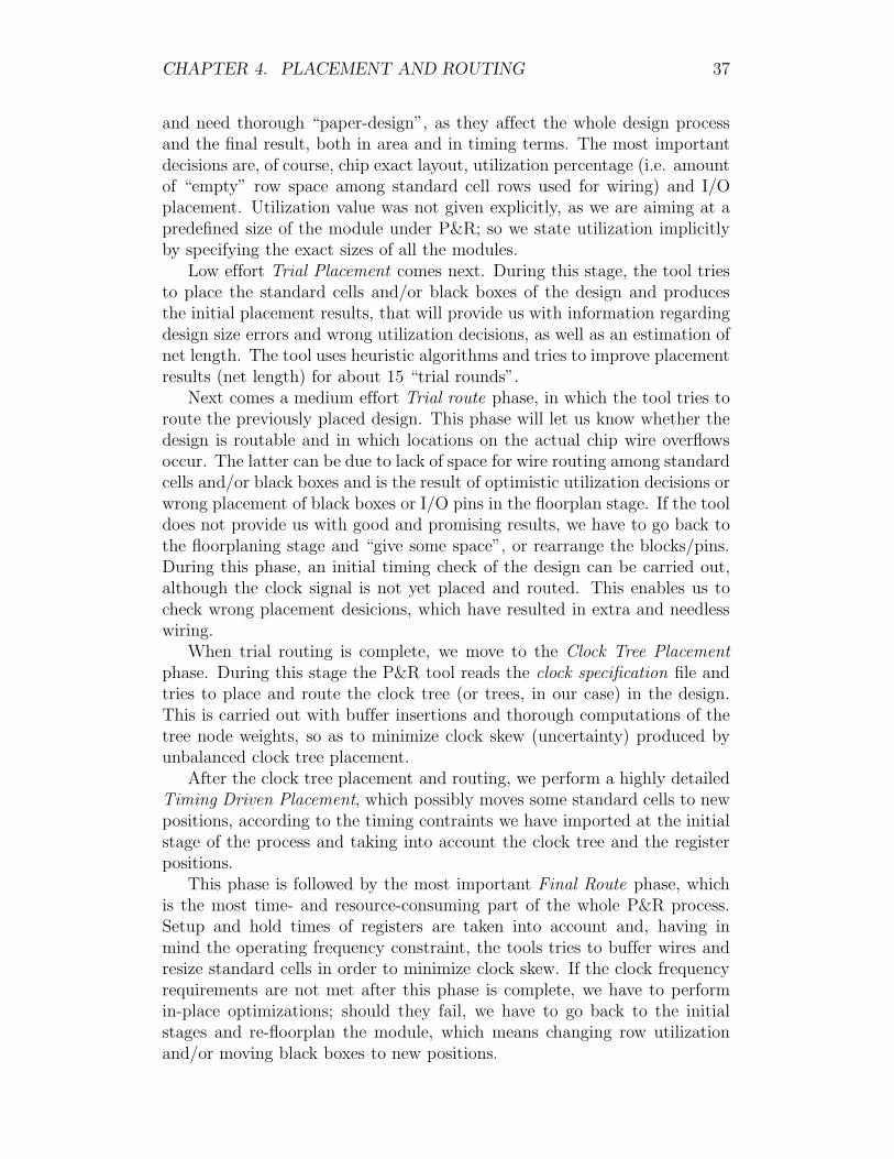
CHAPTER 4. PLACEMENT AND ROUTING 37
and need thorough “paper-design”, as they affect the whole design processand the final result, both in area and in timing terms. The most importantdecisions are, of course, chip exact layout, utilization percentage (i.e. amountof “empty” row space among standard cell rows used for wiring) and I/Oplacement. Utilization value was not given explicitly, as we are aiming at apredefined size of the module under P&R; so we state utilization implicitlyby specifying the exact sizes of all the modules.
Low effort Trial Placement comes next. During this stage, the tool triesto place the standard cells and/or black boxes of the design and producesthe initial placement results, that will provide us with information regardingdesign size errors and wrong utilization decisions, as well as an estimation ofnet length. The tool uses heuristic algorithms and tries to improve placementresults (net length) for about 15 “trial rounds”.
Next comes a medium effort Trial route phase, in which the tool tries toroute the previously placed design. This phase will let us know whether thedesign is routable and in which locations on the actual chip wire overflowsoccur. The latter can be due to lack of space for wire routing among standardcells and/or black boxes and is the result of optimistic utilization decisions orwrong placement of black boxes or I/O pins in the floorplan stage. If the tooldoes not provide us with good and promising results, we have to go back tothe floorplaning stage and “give some space”, or rearrange the blocks/pins.During this phase, an initial timing check of the design can be carried out,although the clock signal is not yet placed and routed. This enables us tocheck wrong placement desicions, which have resulted in extra and needlesswiring.
When trial routing is complete, we move to the Clock Tree Placementphase. During this stage the P&R tool reads the clock specification file andtries to place and route the clock tree (or trees, in our case) in the design.This is carried out with buffer insertions and thorough computations of thetree node weights, so as to minimize clock skew (uncertainty) produced byunbalanced clock tree placement.
After the clock tree placement and routing, we perform a highly detailedTiming Driven Placement, which possibly moves some standard cells to newpositions, according to the timing contraints we have imported at the initialstage of the process and taking into account the clock tree and the registerpositions.
This phase is followed by the most important Final Route phase, whichis the most time- and resource-consuming part of the whole P&R process.Setup and hold times of registers are taken into account and, having inmind the operating frequency constraint, the tools tries to buffer wires andresize standard cells in order to minimize clock skew. If the clock frequencyrequirements are not met after this phase is complete, we have to performin-place optimizations; should they fail, we have to go back to the initialstages and re-floorplan the module, which means changing row utilizationand/or moving black boxes to new positions.
CHAPTER 4. PLACEMENT AND ROUTING 38
4.4 Column Placement and Routing
As mentioned earlier, after thorough investigation of various column place-ment and routing organizations, we came up to a solution that seemed to benearly optimal; this was accomplished by organizing all 32 memories of eachcrossbar column into 2 columns of 16 each and placing the memories withtheir “small” sides on the x-axis (see 4.3(c)).
By this organization, the input lines enter the column from the west side,the data outputs are located on the south side, and the credit outputs comeout from the north side of the column. The input line feedthroughs (datainput lines and sop and eop signals) exit the column’s east side, in order toenter the next column’s respective west inputs. Note that all inputs and theeast outputs are the internal interface of the crosspoint modules, whereasdata and credit outputs come from the output scheduler module.
After placing the memories “by hand”, we also had to restrict the outputscheduler module placement to the lower half of the column; this was carriedout because it was noted that if there were no restrictions imposed on themodule placement, the tool could not place the output scheduler’s standardcells cleverly enough, in order to avoid timing violations. In such cases thedesigner must “assist” the tool, either by restricting the area (up to a rea-sonable size, of course), changing I/O pin placement or even changing thetiming requirements themselves.
Finally, we should note that the credit signals, which originate from theoutput scheduler module, have to be routed across a long way, until theyoutput the column module. As a result, if we do not locate “by hand” the 32output credit pulse registers of each column at the column’s northest position(right “below” the credit outputs), the tool is unable to meet the timinggoals. Actually, this problem is faced in conjunction with the respectivecredit scheduler inputs, which are located in another component on top ofthe crossbar columns (see Figure 4.2). A final placed and routed view of thecolumn can be seen in Figure 4.6.
4.5 Credit Scheduler Placement and Routing
As mentioned earlier, there exist 32 credit schedulers in the crossbar chipand are responsible for sending in a round-robin manner the credit values tothe line card schedulers. There are also two alternatives in this P&R process:flat and hierarchical. Flat P&R of the credit schedulers proves to be a verytime consuming task, as it has to be carried out during the final stage of theP&R, in which case the tool has to handle all 32 column instances and theflat credit schedulers as well. As a result, large layout, netlist and timingfiles have to be processed by the tool, and at the same time, the 32 creditscheduler blocks have to be placed & routed in a flat manner. As a result,we decide to P&R the credit schedulers in a very narrow “line” and then

CHAPTER 4. PLACEMENT AND ROUTING 39
Figure 4.6: Final crosspoint column layout: The picture is rotated 90o clock-wise for space reasons. The output scheduler is located on the left (actualbottom) half of the column, with the data output bus coming from the west(actual south) side. Notice the line in/out metal 6 feedthroughs, that connectto the corresponding line in data inputs of the adjacent column. Dequeuepulse registers were manually located on the east (actual north) column side,in order to avoid inter-block timing violations (their outputs, credit pulses,connect to the credit schedulers, which will be placed on the right (actualnorth) side of the columns.
“hand-place” that block just above the column blocks (see Figure 4.2).By following this organization, the credit scheduler input signals (1024
credit signals) enter the block from the south side, while the credit outputs(32 16-bit buses) come out from the north side. We also have to place thecredit scheduler modules “by hand” at specific positions inside the “line”block and restrict those modules, in order to prevent the tool from movingstandard cells of the 32 modules at far located positions.
Credit scheduler P&R is thus straighforward and is completed easily, alsomeeting the timing requirements. The credit input pulse registers must beplaced as close to the credit scheduler block inputs possible and the toolmanages to comply with this requirement, without human intervention. Asa result, the credit scheduler input registers and the column credit pulseoutput registers (destination and source respectively) are located very closeto each other, thus meeting the clock requirements of these adjacent blocks.Note that those requirements are not met with the initial column placementdecisions and are only solved by placing “by hand” the credit pulse outputregisters, as mentioned in the previous subsection.
4.6 Adding Another Level of Hierarchy: Top
Level Placement and Routing
After organizing the switch core in 32 column modules and one module con-sisting of credit schedulers, we realize that the tool cannot handle the place-ment and routing of so many and so large instances within a respectabletime. This has to do primarily with the machine that was used to P&R the

CHAPTER 4. PLACEMENT AND ROUTING 40
chip 2 and the large size of timing and layout files that have to be analysedby the tool in the final stage. Note that these files are crucial in determiningwhether timing will be met in the final chip.
Figure 4.7: 16-column higher level P&R: Data inputs can be seen connectingto all 16 columns via feedthroughs.
As a result, we conclude that if we add another level of hierarchy in thecolumn organization, the problem will be solved. Organizing the columns inhigher levels of hierarchy is an easy task and is carried out by grouping themduring the synthesis procedure by using the Synopsys group command. Areasonable hierarchy choice is to group the 32 columns in 2 pairs of 16 each,placing and routing these two blocks separately and then combining onlythree highest hierarchy blocks (two groups of 16 columns and one block ofcredit schedulers). This task is carried out successfully; a 16-column resulting
2The only machine we can use has 4 SPARC processors, 400 MHz each, and 3 GB RAM.Use of a faster machine can possibly produce faster results, but hierarchical approach willmost probably be anavoidable.
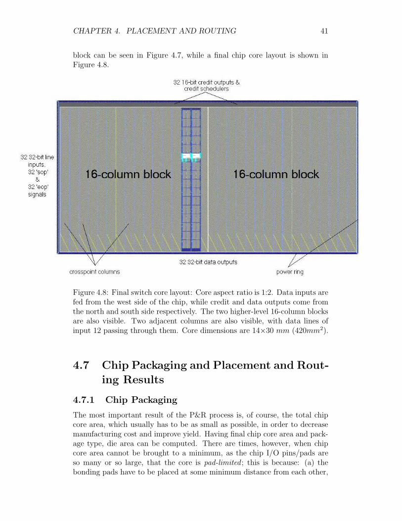
CHAPTER 4. PLACEMENT AND ROUTING 41
block can be seen in Figure 4.7, while a final chip core layout is shown inFigure 4.8.
Figure 4.8: Final switch core layout: Core aspect ratio is 1:2. Data inputs arefed from the west side of the chip, while credit and data outputs come fromthe north and south side respectively. The two higher-level 16-column blocksare also visible. Two adjacent columns are also visible, with data lines ofinput 12 passing through them. Core dimensions are 14×30 mm (420mm2).
4.7 Chip Packaging and Placement and Rout-
ing Results
4.7.1 Chip Packaging
The most important result of the P&R process is, of course, the total chipcore area, which usually has to be as small as possible, in order to decreasemanufacturing cost and improve yield. Having final chip core area and pack-age type, die area can be computed. There are times, however, when chipcore area cannot be brought to a minimum, as the chip I/O pins/pads areso many or so large, that the core is pad-limited ; this is because: (a) thebonding pads have to be placed at some minimum distance from each other,

CHAPTER 4. PLACEMENT AND ROUTING 42
but the periphery of the core cannot fit this requirement; (b) the tranceivercircuits (SERDES) that have to be used occupy periphery larger than thatof the core. The opposite situation is called core-limited and means that thecore is large enough to eventually determine die area.
Note that depending on the number of I/O signals and chip peripherylength, some packaging technologies may result in a pad- and others in a core-limited chip. For example, one of the most popular package types used todayfor ASICs is Ball Grid Array (BGA) [38]. BGA can be either Wire Bond orFlip Chip. In Wire Bond BGA, I/O pins have to be placed at the chip coreperiphery, as shown in Figure 4.9(a), and then connected to bonding padsthrough special I/O cells. Bonding pads are then connected via bond wiresto the BGA package balls. Pads cannot be placed too close to each other:today’s values are 70µm pitch for single-row and 40-50µm staggered pitch iftwo rows are used. This places restrictions on the maximum number of I/Osthat the chip can fit, as they are proportional to its periphery; bonding padnumber is also proportional to die area square root. As a result, although thispackaging method is cheap, it cannot be used when we have large number ofI/Os. Furthermore, bonding wires are relatively long (3-5 mm) and thereforethe connections have high inductance. Flip Chip BGA 4.9(b) can be usedinstead: Although more expensive, this method allows much more I/O pinsto be connected to the (flipped) chip core, which saves die area in pad-limiteddesigns. Signal inductance is also limited, as interconnect length is an orderof magnitude less than that of Wire Bond BGA.
Macro Blocks
Core Logic
Die
Package
PCBTraces
BGAPackage
Balls/Pins
(b)
TracesPackage
70 um
I/O Cells
Core Logic
Die
Package
PCBTraces
BGAPackage
Balls/Pins
Bonding Pads
BondWires
PackageTraces
(a)
I/O Cell/Bump
Figure 4.9: Wire Bond (a) and Flip Chip (b) BGA packaging solutions: ifthe chip proves to be pad-limited in a Wire Bond approach, turning into FlipChip may prevent the core area increase that would have to be adopted if(a) was used.
In the case of the 32×32 buffered crossbar switch, fast and relativelylarge I/O tranceivers (SERDES) have to be used, as input and output datalink speed is nearly 10 Gbit/sec, whereas credit output link speed is 1/4 of

CHAPTER 4. PLACEMENT AND ROUTING 43
the former, namely 2.5 Gbit/sec. If 3.125 Gbit/sec tranceivers (2.5 Gbit/secuseful rate) are used, then 4 and one uni-directional tranceivers are needed forevery data line and credit line respectively. Thus, we need (32+32)×4+32 =288 uni-directional tranceivers for the whole chip, in addition to 64 traditionalwires for the sop and eop signals. If the 32×32 buffered crossbar switch chipis to be placed in a Wire Bond package, then all tranceiver modules will haveto placed on the core periphery. Taking into account that a uni-directional3.125 Gbit/sec tranceiver has an approximated area of 500×500µm in a 0.18µm technology 3, then periphery length must be 144 mm. From the resultspresented shortly, chip core dimensions are 1.4 × 3cm, thus its periphery is88 mm. As a result, our design is pad-limited. Use of the alternative FlipChip packaging method might eliminate this phenomenon.
4.7.2 P&R Results
The 32×32 buffered crossbar chip we place & route has a total area of 420mm2, with an aspect ratio of around 1:2 (1.4×3 cm). Area results, as wellas gate and flip-flop count per module can be seen in Table 4.1.
Module Gates Flip-Flops SRAM Area Area(number (K) (K) 2-port 0.18µm 0.13µmof instances) (bits) (mm2) (mm2)
XPD (1024) 68 91.0 9.5 4.3XPM (1024) 16 M 286.0 130.0OS (32) 100 9.7 4.0 1.8CS (32) 50 6.4 2.0 0.4Clock Tree Buffering 7 0.7 0.3Long Wire Optimization Buffering 38 1.5 0.7Wiring/Hier. Overhead 116.3 53.0
Total 263 107.1 16 M 420.0 190.5
Table 4.1: Placement and routing results: total numbers shown, including allinstances. XPD, XPM, OS and CS refer to crosspoint datapath, crosspointmemories, output schedulers and credit schedulers respectively. Memoryarea is computed from its datasheet [43]. Optimization buffering includesbuffers added after the post-route optimization phase. 0.13µm area resultsare computed by extrapolation.
Note the area differences compared to the corresponding synthesis results(shown in Table 3.1): Area is 40% larger, while gate count has increased by60%. These discrepancies are due to: (a) wiring; (b) hierarchy overhead;and (c) clock tree and optimization buffer insertion. It is reminded that each
3This result is an approximation taken from [27]: there, a single-chip bi-directional
3.125 Gbit/sec tranceiver circuit is 1 × 1mm in 0.18 µm.

CHAPTER 4. PLACEMENT AND ROUTING 44
column had to be fully optimized before importing it to the top-level core. Asa result, in most cases the tool added buffers in all hierarchy levels in order tomeet timing constraints; these buffers, although usually small, are numerous:if we take into account only each column interface, then buffering each columnoutputs adds almost 35000 buffers in the switch core, thus increasing its areaand power consumption 4.
4.8 Conclusions: Dealing With Large and Reg-
ular Designs
The P&R process presented in the previous subsections poses many differencescompared to flat P&R, which is usually followed in the case of small designs.First of all, this process was imposed because of the large number of gates,but, mainly, by the large number of black boxes (memories) which lie in theswitch. The latter results from the O(N2) complexity of the crossbar switch,which is an inherent characteristic of the crossbar architecture. HierarchicalP&R has itself many challenges, the most important being the correct deci-sion of the hierarchy that must be chosen in order to help, not the designer,but the tool, in performing quick and resource-aware P&R.
Wiring seems to be the most crucial factor of the hierarchical P&R pro-cess. Wires that interconnect low-level modules must be taken into account,in order to prevent the tool from using unneedlessly long wiring while con-necting the modules. In our case, from the solutions investigated, manualcreation of feedthroughs within the modules seemed to be the most appro-priate, as it led to straightforward layout with small area overhead. Anotherimportant factor that must be taken into account is the final pin layout,which inevitably influences the P&R process speed and success. It should benoted that hierarchical decisions taken during P&R phase may not be thesame as the ones taken during synthesis. These hierarchical changes can beperformed both in the RTL and the Gate Level, the first having the disadvan-tage that a slight change in hierarchy directly affects RTL, needing carefuland error-prone changes. In the Gate Level, hierarchy changes can be easilycarried out by using the Synopsys group command.
Of course, hierarchical P&R most often leeds to larger designs, as there isarea overhead that has to be added in order to P&R lower hierarchy blocks.Unfortunately, in our case, we had to make a tradeoff between following hi-erarchical P&R, because of the tool’s limitations, and producing the smallestchip possible, as the design area (during synthesis) was already closing 300mm2. Thus, the tremendous difference between the Gate Level area resultand the final placed & routed chip area result (300mm2 and 420mm2 respec-tively), should not surprise us: a growth of 40-50% should be a rule of thumbin large designs, especially when a hierarchical P&R approach is followed.
4Buffer insertion effect on power consumption is discussed in the next chapter.

CHAPTER 4. PLACEMENT AND ROUTING 45
Place & route flow is, undebatably, the most time consuming part ofthe chip design, as: (a) it demands careful “hand” design and analysis ofthe alternative organization ways; and (b) each stage is time consumingand usually the designer has to restart the flow from the very beginning ifsomething goes wrong. This “back-and-forth” situation can be carried outtens of times before the first promising results are reported; therefore, forindustrial designs, careful management of the project has to be performedin order to meet time to market demands; the faster the design is designed,verified and synthesised, the better.
Finally, it should be noted that the regularity of the design actually as-sisted us, both by making hierarchy decisions easy and by helping the toolwith the P&R process, as the number of different modules in each level waslimited: For example, each “column” comprised of 32 identical crosspointmodules and one output scheduler module, whereas the switch was made upof 32 “columns” and one credit scheduler “line”. If there was no regular-ity, P&R of such a large design would probably have been much more timeconsuming.

Chapter 5
Power Consumption
Total power consumption is the sum of two different types of power: dynamicand static [47]. Dynamic power is dissipated when the circuit is active, thatis, when the voltage on a net changes due to stimulus applied to the circuit.Notice that because voltage on a net can change without necessarily result-ing in a logic transition of the output, dynamic power can be dissipated evenwhen an output net doesn’t change its logic value (see Figure 5.1). Staticpower is the power dissipated by a gate when it is not switching, that is,when it is inactive or static. Static power can be dissipated in several ways;the largest percentage results from the source-to-drain transistor subthresh-old leakage caused by reduced threshold voltages preventing the gate fromcompletely turning off. Static power is also dissipated when current leaks be-tween the diffusion layers and the substrate of a transistor; For this reason,static power is often called leakage power.
D
A
B
C
Figure 5.1: Dynamic power is dissipated even if the output does not change:Logic cell inputs A, B and C can switch from logic 0 to 1, and net D canswitch from 1 to 0, but the output will remain unaffected, althought dynamicpower was consumpted.
The dynamic power dissipation of a circuit is composed of two factors:switching power and internal power. Switching power results from charg-ing and discharging the load capacitance of an output cell 1 and equals toPSW = pswfckCV 2
DD, where psw is the probability that a node will switch upand down, fck is the clock frequency, C is the load capacitance and VDD is the
1Cells are complex or simple gates in which logic is transformed by synthesis.
46

CHAPTER 5. POWER CONSUMPTION 47
supply voltage. Internal power is any power dissipated within the boundaryof a cell. During switching, a circuit dissipates internal power by the charg-ing and discharging of any existing capacitances internal to the cell. Internalpower includes power dissipated by a momentary short circuit between theP and N transistors of a gate, called short-circuit power.
Switching power is the dominant (90% and relatively decreasing) com-ponent in current CMOS technologies. Internal (mainly short-circuit) powerconstitutes about 8% of the total power consumption, with an absolute de-creasing trend; the rest 2% (although relatively increasing) comes from leak-age (static) power. Although for circuits with fast transistion times (i.e. fastclocks), short-circuit power consumption can be small, for slow-transitionones the short-circuit power dissipation can account for as high as 30% ofthe total power dissipated by the gate. Short-circuit power is affected bythe dimensions of the transistors and the load capacitance of the gate’s out-put. If we ignore short-circuit and leakage power consumption, we observethat for the same technology and same circuit working characteristics (i.e.the same clock frequency, supply voltage and switching activity), switchingcapacitance is the only factor that can be controlled and reduced (bufferingof long nets is a possible solution) 2. Short-circuit power dissipation is il-lustrated in Figure 5.2: if we apply positive voltage at the input then, asthe signal transitions from low to high, the N-type transistor turns on andthe P-type transistor turns off. However, for a short time during the inputtransistion, both P- and N-type transistors are switched on simultaneously.During this time, current ISC flows from VDD to GND, causing the dissipa-tion of short-circuit power (PSC). Figure 5.2 also illustrates where exactly
t
V
t
OUTIN ISC
ILK
ILK
N
P
CLOAD
ISW
VDD
GND
V
Figure 5.2: Components of power dissipation illustrated in the case of aninverter: ILK, ISC , and ISW are leakage, short-circuit and switching currentsrespectively.
dynamic (switching and short-circuit) power is dissipated.
2Capacitance limitation is also the key factor that has to be minimized in order toavoid timing violations.

CHAPTER 5. POWER CONSUMPTION 48
In the following sections we will talk about the work carried out in mea-suring and reducing switch (especially crossbar) power consumption, brieflyintroduce the Gate Level and Placement & Routing power estimation flows,and present the power estimation results of our 32×32 buffered crossbar de-sign. In the appendix we talk about the most important power minimizationtechniques that can be applied in the RTL and Gate Level design stages.
5.1 Crossbar Switch Power Consumption Es-
timation: Work Done Sofar
Various researchers have tried to come up with crossbar power consumptionconclusions, as well as discover the most power consuming components ofsuch devices. Ye et al. [44] performed Verilog RTL simulations on the fourmost important switch fabric topologies (crossbar, fully connected, Banyanand Batcher-Banyan) and introduced a framework to estimate their powerconsumption 3. They divided a switch into four main parts (ingress and egresspacket processing units, arbiter and switch fabric) and analysed only the lat-ter component. “Bit Energy” is also introduced; it comprises of the energyconsumed by a single bit travelling on switching nodes, in buffer memoriesand on interconnection wires. They concluded that (a) interconnect con-tention increases significantly switch power consumption 4; (b) for switcheswith small number of ports, internal node switching dominates, while inmulti-port switches (beyond 32×32), interconnect power is the dominant fac-tor. Their simulation results show that a 32×32 bufferless crossbar switchingfabric consumes approximately 300 mW, under uniform traffic conditions andload almost 60%.
Wang et al. [45] developed an architectural-level power-performance sim-ulator for switches and routers, called Orion. They introduced router powermodels of the three most power consuming router building blocks, namelymemories, crossbars and arbiters. The authors applied their theoretical mod-els to two commercial routers, the Alpha 21364 and the IBM Infiniband 8-port 12X. Their most interesting (for the purposes of this work) result wasthe power estimation of the Alpha 21364’s switching fabric, which comprisesof two 8×5 crossbars: the estimated average power consumption was about700 mW, for 100% input load, whereas worst case power estimation is almostdouble the figures of the average case. Their results were close to the esti-mated values published by the companies that design these products. Theyalso came to the conclusion that: (a) crossbar and buffer memory powerconsumption grow approximately linearly to the data arrival rate, as theyare both “datapath” components; (b) the larger the memory, the higher the
3Switch I/O consumption is not taken into account in their study.4Nevertheless, a crossbar switching fabric does not suffer from internal blocking, hence
interconnect contention is negligible in our case.

CHAPTER 5. POWER CONSUMPTION 49
power it will comparably consume; (c) router links 5 consume a large amount(almost double) of the switch core total power consumption. Based on theabove assumptions, we can conclude that our switch’s crosspoint datapathpower consumption will be at least 500 mW 6.
Various researchers have provided approximate I/O and power consump-tion figures and predictions, in order to assist designers in performing efficientpower budgeting. According to [35], single-chip I/O power consumption fac-tor is expected to grow, from 16% in the case of a 6 Gbit/sec 16×16 switch,to 50% for a 64 Gbit/sec 32×32 switch. [18] states that any state-of-the-artswitch is severely limited by I/O pins and their power consumption: high-speed and high-density SERDES (tranceivers) available in ASIC librariestoday give approximately 125 mW per 2.5 Gbit/sec useful bandwidth full-duplex (3.125 Gbit/sec in 8B/10B encoding); as a result, a 4 Tbit/sec switchwould require about 104 pins and would dissipate roughly 256 W of I/Opower! This is obviously prohibitive for single-chip implementations: in or-der to comply with Network Equipment Building Standards (NEBS) rules[33], a single board must not dissipate more than 150-250 W, while single-chippower dissipation must remain under 25 W to avoid hot spots and expensivecooling solutions.
Last of all, [31] states that on-chip buffer memories (0.18µm) consume5-10 mW in order to support sustainable Gbit bandwidth, while the samefigure for chip I/O power consumption grows to 40 mW/Gbps in 0.18µm and25 mW/Gbps in 0.13µm. Thus, I/O throughput is 5 to 10 times higher thanon-chip buffer memory throughput in terms of power consumption, whicheventually limits the total achievable single-chip switch throughput: a singleswitch chip with 64 10 Gbit/sec incoming links will have an approximate I/Opower consumption of 32 W in a 0.13µm technology. To make matters worse,in order to limit package pin count, the designers would favor high-speedlinks (e.g. 3.125 Gbit/sec SERDES/ tranceivers), which are large enough(almost 1mm2 per 3.125 Gbit/sec tranceiver in 0.18µm [27]) to result in apad-limited chip core. Hence, I/O power consumption is possibly one of themost important factors when designing single-chip switches; moreover, in abuffered crossbar, special care should be taken for memory consumption, aswell.
5.2 Power Analysis Flow: RTL vs. Gate Level
vs. Post-P&R
Power analysis can be carried out in many design stages, the lowest levelsbeing RTL, Gate Level and post-P&R. The more “abstract” the circuit’s
5Links include expensive Serializer-Deserializer (SERDES) circuits; the term “tran-ceiver” is usually used instead.
6The actual figure will grow, due to the extra logic included in each crosspoint; suchlogic is not needed in the unbuffered crossbar implementations analyzed above.

CHAPTER 5. POWER CONSUMPTION 50
description is, the more imprecise the power analysis results are; hence, RTLpower estimation is considered erroneous, whereas the Gate Level and post-P&R ones are more accurate. In this thesis we estimated the power con-sumption on both the Gate Level and post-P&R level (on some design com-ponents). In the remainder of this section we will briefly present these poweranalysis flows, both in the Gate and post-P&R level.
5.2.1 Gate Level Power Estimation
The Gate Level power estimation is carried out by the Synopsys Power Com-piler, which is included in the framework of the Synopsys Design Compiler[47]. Synopsys Power Compiler uses various formulas and the informationmodeled in the logic cell technology library, in order to evaluate the staticpower of a design. Apart from using equations, Power Compiler uses two- orthree-dimentional lookup tables that contain power consumption values forvarious output load capacitances and input transition times. Note that cellsoften consume different amounts of internal power depending on which inputpin transitions take place or depending on the state of the cell; hence, inter-nal power is state- and path- dependent. For example, in a cell with manylevels of logic (see Figure 5.1), a transition on an input signal that affectsmany levels consumes more power than that of an input signal that affectsless levels; Power Compiler takes such differences into account. An exam-ple of a cell with varying state-dependent internal power consumption is aRAM, where different amounts of power is dissipated depending on whetherit is in read or write mode. Dynamic power is computed by the formulamentioned in the introductory section; capacitance information is obtainedby the wireload model 7 specified by the user or the tool, as well as by thetechnology library information for the gates connected to the net 8.
Cell internal power and net toggling (i.e. the frequency of the inputtransitions) have a direct effect on the dynamic power of a design. PowerCompiler needs such information in order to perform power reporting or op-timizations; net toggling is also called switching activity. Switching activitycan be given to the tool in two ways: (a) by specifying the toggle rate in termsof static probability, in which case the results are probably inaccurate; and(b) by measuring the switching activity under a certain simulation scenarioand back-annotating it to the power estimation tool; measurements can becarried out on some or all design objects. Switching activity annotation isperformed by compiling and simulating the design within an HDL simulatorthat can capture switching activity; in our case, Cadence Verilog XL [20]verilog_toggle command was used. We can also include interconnect andcell delay information into the annotation tool; this is carried out by loading
7A large wireload model, e.g. 80K, should thus be preffered upon a smaller one incases when the module under synthesis includes large amounts of wiring. This decision,however, cannot be usually made unless physical layout decisions have been made.
8Capacitance information can be also back-annotated after physical design.

CHAPTER 5. POWER CONSUMPTION 51
the “Standard Delay Format” file (.sdf) written out by Design Compiler dur-ing the synthesis phase. Furthermore, a library forward-annotation file, thatcontains information from the technology library regarding the cells’ state-and path-dependent power models, can be used; this file, as well as the sim-ulator switching activity annotation result file, is written in the SwitchingActivity Interchange Format, hence its extension is .saif. After switchingactivity is annotated, it is loaded into the Power Compiler, read and ana-lyzed. The power estimation flow is shown in Figure 5.3. In the Appendix,we describe this procedure in detail.
power estimation & report
−Gate level netlist (.v)−Net interconnect file (.sdf)−Library forward−annotation file (.saif)
Capture switching activitythrough HDL simulation
(e.g. verilog_toggle)
Back−annotation SAIF file
Power Compiler
Figure 5.3: General Gate level power estimation flow.
5.2.2 Post-P&R Power Estimation
The post-P&R power estimation is carried out after the circuit is placedand routed. This kind of power estimation requires the same information asthe Gate Level one; that is, the net and cell delay file (.sdf), the libraryannotation file (.saif) and, of course, the post-P&R netlist of the design(.v). The latter file, as well as the Standard Delay Format (.sdf) file areproduced by the P&R tool; the .saif file is the same one that was used forsynthesis. The power estimation procedure is carried out in the Synopsysenvironment by the Power Compiler tool, and the steps described in the lastsection are followed.

CHAPTER 5. POWER CONSUMPTION 52
5.3 Switch Power Consumption Breakdown
We measure both Gate Level and post-P&R steady-state 9 power consump-tion of the 32×32 buffered crossbar switch; in this section we present themost accurate post-P&R results 10. Power estimation is carried out by send-ing minimum-size packets (40 Bytes) back-to-back (100% load), from everyinput to uniformly selected outputs. Packet payload is selected so as tomaximize net switching.
The power consumption breakdown can be seen in figures 5.4 and 5.5.
Total chip power consumption: 28.75 W
XPM1
OS CS0.40.5
OutputLineInput Line Wiring
0.6Wiring3
Chip core power consumption: 5.75 WSERDES power consumption: 23 W
0.25XPD
Figure 5.4: Power consumption breakdown: XPD = crosspoint datapath,XPM = crosspoint memories, OS = output schedulers, CS = credit sched-ulers. All numbers are in Watt.
XPMXPD
Input Line Wiring
CS
OS
Wiring
OutputLine
52%
10%
9%
7%
17%5%
Figure 5.5: Power consumption percentage breakdown of the 32×32 bufferedcrossbar switch.
Crosspoint datapath consumes 250mW of power, while output and creditschedulers dissipate 500 and 400mW respectively. Crosspoint memories con-
9“Steady-state” power consumption differs from the absolute worst-case one; this isanalyzed shortly.
10Post-P&R power estimation is followed in order to measure the consumption of eachswitch component. Power estimation of the total switch core, however, is carried out atthe Gate Level.
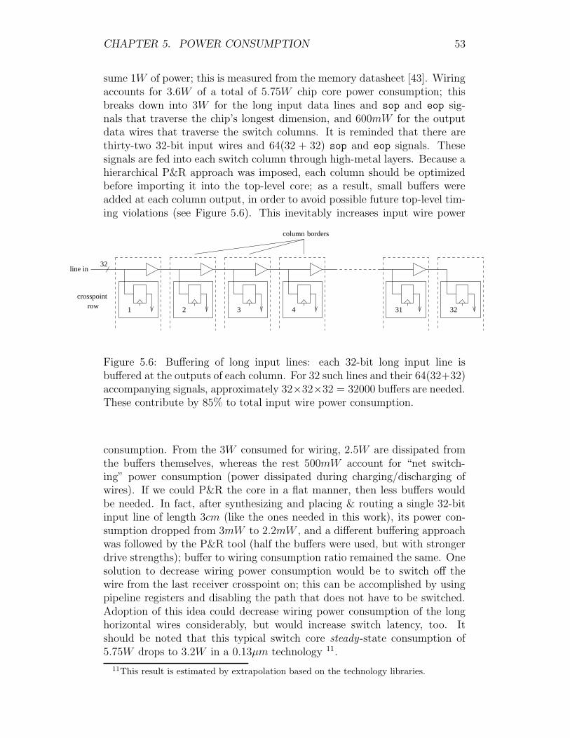
CHAPTER 5. POWER CONSUMPTION 53
sume 1W of power; this is measured from the memory datasheet [43]. Wiringaccounts for 3.6W of a total of 5.75W chip core power consumption; thisbreaks down into 3W for the long input data lines and sop and eop sig-nals that traverse the chip’s longest dimension, and 600mW for the outputdata wires that traverse the switch columns. It is reminded that there arethirty-two 32-bit input wires and 64(32 + 32) sop and eop signals. Thesesignals are fed into each switch column through high-metal layers. Because ahierarchical P&R approach was imposed, each column should be optimizedbefore importing it into the top-level core; as a result, small buffers wereadded at each column output, in order to avoid possible future top-level tim-ing violations (see Figure 5.6). This inevitably increases input wire power
borders
32line in
1 3
crosspointrow 2 4 31 32
column
Figure 5.6: Buffering of long input lines: each 32-bit long input line isbuffered at the outputs of each column. For 32 such lines and their 64(32+32)accompanying signals, approximately 32×32×32 = 32000 buffers are needed.These contribute by 85% to total input wire power consumption.
consumption. From the 3W consumed for wiring, 2.5W are dissipated fromthe buffers themselves, whereas the rest 500mW account for “net switch-ing” power consumption (power dissipated during charging/discharging ofwires). If we could P&R the core in a flat manner, then less buffers wouldbe needed. In fact, after synthesizing and placing & routing a single 32-bitinput line of length 3cm (like the ones needed in this work), its power con-sumption dropped from 3mW to 2.2mW , and a different buffering approachwas followed by the P&R tool (half the buffers were used, but with strongerdrive strengths); buffer to wiring consumption ratio remained the same. Onesolution to decrease wiring power consumption would be to switch off thewire from the last receiver crosspoint on; this can be accomplished by usingpipeline registers and disabling the path that does not have to be switched.Adoption of this idea could decrease wiring power consumption of the longhorizontal wires considerably, but would increase switch latency, too. Itshould be noted that this typical switch core steady-state consumption of5.75W drops to 3.2W in a 0.13µm technology 11.
11This result is estimated by extrapolation based on the technology libraries.
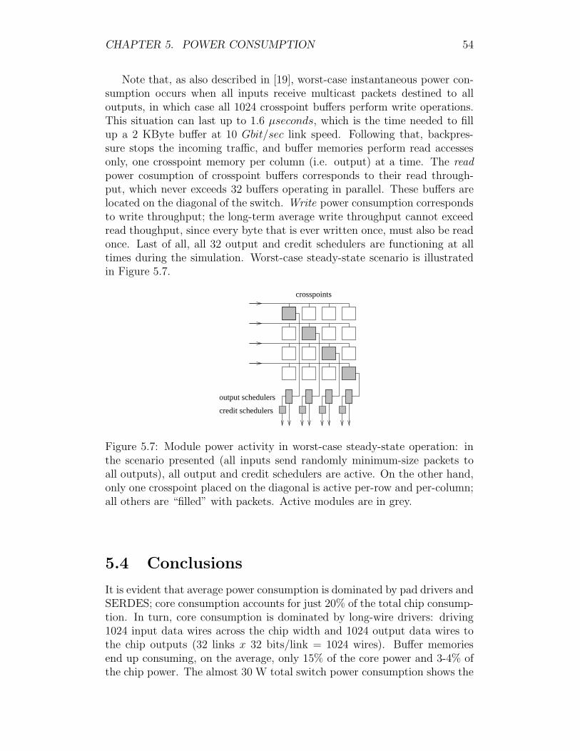
CHAPTER 5. POWER CONSUMPTION 54
Note that, as also described in [19], worst-case instantaneous power con-sumption occurs when all inputs receive multicast packets destined to alloutputs, in which case all 1024 crosspoint buffers perform write operations.This situation can last up to 1.6 µseconds, which is the time needed to fillup a 2 KByte buffer at 10 Gbit/sec link speed. Following that, backpres-sure stops the incoming traffic, and buffer memories perform read accessesonly, one crosspoint memory per column (i.e. output) at a time. The readpower cosumption of crosspoint buffers corresponds to their read through-put, which never exceeds 32 buffers operating in parallel. These buffers arelocated on the diagonal of the switch. Write power consumption correspondsto write throughput; the long-term average write throughput cannot exceedread thoughput, since every byte that is ever written once, must also be readonce. Last of all, all 32 output and credit schedulers are functioning at alltimes during the simulation. Worst-case steady-state scenario is illustratedin Figure 5.7.
output schedulers
credit schedulers
crosspoints
Figure 5.7: Module power activity in worst-case steady-state operation: inthe scenario presented (all inputs send randomly minimum-size packets toall outputs), all output and credit schedulers are active. On the other hand,only one crosspoint placed on the diagonal is active per-row and per-column;all others are “filled” with packets. Active modules are in grey.
5.4 Conclusions
It is evident that average power consumption is dominated by pad drivers andSERDES; core consumption accounts for just 20% of the total chip consump-tion. In turn, core consumption is dominated by long-wire drivers: driving1024 input data wires across the chip width and 1024 output data wires tothe chip outputs (32 links x 32 bits/link = 1024 wires). Buffer memoriesend up consuming, on the average, only 15% of the core power and 3-4% ofthe chip power. The almost 30 W total switch power consumption shows the

CHAPTER 5. POWER CONSUMPTION 55
feasibility of our design, as with a medium-priced packaging technology, itspower dissipation will not cause any problems.

Chapter 6
Conclusions and Future Work
In this work we presented a novel buffered crossbar organization, and provedits feasibility by designing a 32×32 speedup-less such switch core, with ag-gregate incoming throughput of 300 Gbit/sec; final chip core area was 420mm2 in a 0.18 µm and 200 mm2 in a 0.13 µm CMOS technology, while itspower consumption dropped just below 6 Watts (3.2 W in 0.13 µm). Tak-ing into account that a similar switch would approximate 110 mm2 in theemerging 0.09 µm technologies, we can claim that the adopted organizationcan become the switching building block of the future.
The fact that output scheduling was distributed over every output, re-moved the need for a very fast, complicated scheduler, that would control allconnection requests; as a result, speedup due to scheduling inefficiencies waseliminated. Switch novelty stems from the fact that no packet segmentationand reassembly (SAR) had to be carried out; hence no speedup due to SARhad to be adopted, either.
We divided the switch into 2 clock domains: the use of 2-port SRAMsat each crosspoint removed the need for elastic buffers at the switch inputs,in order to synchronize all incoming data to a single local clock; the onlyother synchronization needed concerned a single-bit control signal at eachcrosspoint, and was dealt with an effective 1-bit synchronizer. The simpleand effective Round Robin policy was followed at both the output and creditschedulers. The latter sends credits to the input line cards in a QFC-likemanner, thus compensating for possible credit losses.
We synthesized and placed and routed the switch by following hierarchi-cal flows, which was due to the large number of memories (1024) and theresulting chip size. Such flows are usually carried during the developmentof large or complicated designs, and were completely new approaches to us.Hierarchical flows posed some difficulties though, in particular choosing theoptimal hierarchy organization that would assist the tools in producing fastresults. P&R, being more complicated, error-prone, and time consuming,covered almost half of this work’s duration.
Multiple priority support is a usual feature of commercial switches. Tosupport multiple priorities under the proposed architecture and maintain full
56

CHAPTER 6. CONCLUSIONS AND FUTURE WORK 57
efficiency (no HOL or buffer hogging) we need L∗2KB of buffer space, whereL is the number of priorities. For example, if 8 priorities were used, thenour implementation would need 8 × 2× 1024 = 16MBytes of total memory,which will be only feasible in future CMOS and/or memory technologies.Fortunately, as Chrysos et al. [24] have shown, only two 2KByte buffers areneeded per crosspoint: through simulation, and assuming 8 priority levels,the 2× 2KByte per-crosspoint proposed system performs almost identicallyto the 8×2KByte per-crosspoint ideal system under realistic traffic, whereas,even under highly irregular traffic, average delay of any priority level is notincreased by more than 75%, compared to the ideal system. If this organi-zation is adopted, then 8 priorities will only need 32 Mbits of total SRAMmemory, divided into 2048 2Kbyte SRAMs, which is feasible in current state-of-the-art CMOS technologies (0.13/0.09µm).
Also, another interesting point is the fact that, in fast networks, maximumpacket size has been increased from 1500 Bytes, to almost 9 KBytes. Thisposes significant difficulties in case the proposed organization is followed,due to the fact that buffer size equals RTT + MaximumPacketSize; hence,under medium RTT values, each buffer would have to be almost 10 KBytes,as a result, a 32×32 single-priority, buffered crossbar would need 80 Mbitsof distributed, on-chip SRAM memory, in order to operate efficiently underheavy load. This memory area is too large, even if we take into account thetechnology downscaling fashion. Embedded DRAM (eDRAM) is a possiblesolution as, being up to 4 times denser than conventional SRAM, could lowerchip area to normal sizes. eDRAM adoption would, of course, impact on thecrossbar organization, as well.
Appendix A
Organization of a 4-input WRRScheduler
As noted in chapter 2, during the initial stages of this thesis we investi-gated the design and implementation of a 4×4 buffered crossbar switch thatwould be downloaded in an Altera FPGA. The number of input/output ports(switch size) was bounded by the memory requirements, as 32 KBytes areneeded for a 16-crosspoint switch. Operating frequency was specified to 50MHz, hence the switch would have link speed of 1.5 Gbit/sec link. Althoughthis attempt was later abandoned (and replaced by the more “ambitious”32×32 buffered crossbar ASIC chip design & implementation), a 4-inputWeighted Round Robin output scheduler was designed, in order to select theappropriate flow among the 4 crosspoints of each column of the 4×4 switch.In the next sections we will briefly present various scheduling policies thatare being used in network traffic management circuits, followed by a shortintroduction to Weighted Round Robin (WRR) discipline. Finally, we willpresent the internal organization and operation of our 4-input WRR outputscheduler.
A.1 Introduction to Scheduling Policies
In this subsection we will assume N flows and P priorities; each flow has one ofthese P priorities [31]. The simplest scheduling discipline is the strict (static)priority scheduling, where each flow 1 belongs to a certain static prioritylevel. The scheduler’s goal is to serve the highest-priority eligible flow. Thisdiscipline is very easy to implement by using a priority enforcer/encoder.Unfortunately, the strict priority scheduling scheme suffers from a starvationissue: if flow i is not policed or regulated and becomes persistent (i.e. alwayshas a non-empty, eligible queue), then all levels below i will be starved; thatis why we have to ensure that all levels but the last (lowest priority) one willbe be policed or regulated.
1Each flow may be an aggregate of many sub-flows
58

APPENDIX A. ORGANIZATION OF A 4-INPUT WRR SCHEDULER59
The other extreme of priority scheduling is plain round robin (equality)scheduling, which was actually the only scheduling discipline used in the32×32 buffered crossbar switch presented in this thesis. In plain round robin,the scheduler visits each eligible flow, regardless of its priority or persistency;hence, all flows have the same priority. Round robin scheduling can be im-plemented in two ways: (a) by using a circular priority encoder/enforcer and(b) by using a linked list of the eligible flow IDs. Method (a) needs simplecircuitry (round robin priority enforcers), while efficient organizations existfor small, medium, or large number of flows. Implementation (b) has thedifficulty of where to reinsert a flow that was ineligible and has just becomeeligible, with most of the possible solutions leading to unfairness.
A.2 Weighted Round Robin Scheduling
Last of all, there is a way to serve each flow according to its priority, butwith a round robin manner as well. If each flow had a weight, that wouldcorrespond to its priority, then the round robin policy could be changedby the following way: assume that we maintain a (varying) set of eligibleflows and we associate a value, called “Next Service Time” (NST) with eachof them. Then, in summary, the scheduler has to (a) find and serve the(eligible) flow that has the minimum (earliest) NST, and (b) re-schedule fora future time the flow just served.
When scheduling starts, each flow is possibly served randomly 2. Whena flow is served, the (virtual) time it will be served again is computed bymultiplying its weight 3 by the packet size that is being dequeued by theflow and adding the result to its current “service time”. Thus, intuitivelly,the flow will be served some (virtual) time in the future, relative to thetime it was being served and its priority (weight). An WRR schedulingexample is shown in Figure A.1, where 4 flows, A to D , with various weightsand eligibility statuses are being scheduled. Flow initial service order israndom. Last of all, it should be noted that according to the reinsertiontime of a flow that was ineligible and suddenly becomes eligible, as well asthe Next Service Time computation, many variants of WRR scheduling havebeen examined in the past, with the most important being “Weighted FairQueueing (WFQ)”, “Self-Clocked Fair Queueing (SCFQ)”, “Worst-Case FairWeighted Fair Queueing (WF2Q)”, “Start-time Fair Queueing (SFQ)” and“Virtual Clock”.
2In the case of multiple low-rate flows and less high-rate flows, unfavorable initilizationmay cause large jitter to the latter; aggregation of low-rate flows and round robin serviceinside them solves the problem.
3Sometimes the inverse value is used, called “Service Interval” (SI).

APPENDIX A. ORGANIZATION OF A 4-INPUT WRR SCHEDULER60
flow B SI
B
C
D
Eligibilitystatus
WeightFactor
50
30
10
10
Interval (SI)Service
20
33
100
100NO
YES
YES
YESA
Flow
A
0
A C B
105 20 4043
A B A
60
B A
76 80
A
100105 109
BC
120
A A B
140 142 175
B D
190
C
205 208
B B
241servicetime
(virtual)
eligiblebecomes
ineligiblebecomes
flow A SI
flow C SIflow D SI
Figure A.1: Priority queue WRR scheduling example: Flows A to D haveweights 50%, 30%, 10% and 10% respectively; hence their Service Intervals(SIs) are 20, 33, 100 and 100. Initial service is random. Notice that flow A,which was served at (virtual) time 0, will be served again in time 0+20 = 20,whereas flow B was served at time 10 and will be re-served at 10 + 33 = 43.
A.3 4×4 Output Scheduler Organization
Output scheduler block diagra can be seen in Figure A.2. The scheduler has4 32-bit input data buses, accompanied by 4 synchronized “Start Of Packet”(sop) signals. The block outputs a 32-bit data_out bus to the switch outputs,as well as a 4-bit wide deq bus, which connects to the corresponding rd_en
signals of the column crosspoints’ memories.
WRR
32
32
32
32line_out 4
line_out 3
line_out 2
line_out 1
32data_out
4 4
clk_rd
reset
syncsop
deq
4−INPUT
SCHEDULEROUTPUT
Figure A.2: 4-input WRR output scheduler block diagram.
Figure A.3 presents the WRR scheduler internal organization. Flow eligi-bility flags are computed via 4 packet adders: if an adder equals zero, its flowis ineligible. Packet counters are incremented by the synchronized sop signalthat the column crosspoint that enqueues the packet sends to the outputscheduler. This eligibility flag fires the FSM that controlls packet dequeuesand WRR operation.

APPENDIX A. ORGANIZATION OF A 4-INPUT WRR SCHEDULER61
The most important operation of the specific scheduler is the computationof the minimum NST, among 4 values. This can be accomplished in two ways:(a) by using 3 comparators, organized in a tree fashion, along with three 32-bit multiplexors (top left of Figure A.3); (b) by using 6 comparators, whichcompare all 4 NST values with each other (center of Figure A.3). Althoughthe first method needs only half the comparators compared to solution (b), italso requires 3 2-input, 32-bit multiplexors, which are considered expensivein this context; hence, we eventually used method (b). By comparing allNST values (from now on called NST_1 to NST_4) with each other, 6 “lessthan” signals are generated: NST_4 less than NST_3, NST_4 less than NST_2,NST_4 less than NST_1, NST_3 less than NST_2, NST_3 less than NST_1 andNST_2 less than NST_1. These signals, along with the 4 eligibility flags, arefed into a combinational logic 3-level circuit, which chooses the next eligible,minimum NST value. For example, the logic used for NST_4 is as follows:
if (NST_4 eligible)
if (NST_3 eligible AND NST_4 < NST_3) OR NST_3 ineligible, OR
if (NST_2 eligible AND NST_4 < NST_2) OR NST_2 ineligible, OR
if (NST_1 eligible AND NST_4 < NST_1) OR NST_1 ineligible, OR
then min_NST = NST_4
...
where min_NST is the minimum Next Service Time among the 4 flows. Threesimilar if clauses are used for the rest of the flows. The flow_sel resultof the combinational logic curcuit is used to select (a) the line_out busthat will be sent to the scheduler output, (b) the SI value that will be usedfor multiplication with the packet’s size, (c) the NST register that will beupdated with the new NST value.
Four 16-bit registers are used to store the SIs; these values are multipliedby packet size, in order to compute the NST of the flow currently beingdequeued. The multiplier has a two clock cycle latency and its exit is the16x16 = 32−bit value that must be added to the previous NST of the specificflow. After the NST is updated, all ineligible NSTs have to be brought tothe current NST, too (Weighted Fair Queueing policy).
Dequeueing stops either when the packet is fully dequeued (eop_deq)and there is no other eligible flow, or when there still exist eligible flows,thus next-flow minimum NST computation has to start before the currentlydequeueing finishes (pre_schedule ).
Last of all, it should be noted that the 32-bit adder, the 16-bit multiplierand the 32-bit comparators all have a 2 clock cycle latency, thus they allneed 40 nsec to produce a result. This constraint was imposed by FPGAlimitations.

APPENDIX A. ORGANIZATION OF A 4-INPUT WRR SCHEDULER62
32
CMP
CMP
CMP
CMP
CMP
+/− +/− +/−+/−
CMP
CMP
CMP
CMP
���� ����
��
�� �
��
����
��
������
��� !"
1
2
3
4
adder32−bit
line_out 1
line_out 2
line_out 3
line_out 4
32
32
32
32
16
pck_sz
INTERVALS
32
flow_sel
32
min_NST
SERVICENEXT
TIMES
4<3
4<2
4<13<2
3<1
2<1
2
flow_sel
CL3−level
updateNSTs
comparators32−bit
16
SERVICE
flow_sel
2
mult16−bit
2flow_sel
(from column XPs)
(to column XPs)deq [3:0]
sop_sync 1sop_sync 2sop_sync 3sop_sync 4
(from column XPs)
32
(to switch output)data_out
(from FSM)
4counterspacket
Alternative
2<1
4<3
result
1
2
3
4
structurecomparator
eop_deq/pre_schedule
dec
1SI SI
3SI
4SI
2
2
elig. states
32
NSTmin
32 32
32
32
32
32
Figure A.3: Weighted Round Robin (WRR) output scheduler internal or-ganization. 6 comparators are used in order to compare all 4 Next ServiceTimes (NST) with each other. This comparison stage can be otherwise im-plemented by using 3 comparators, in a tree order, and 2 32-bit multiplexors.This organization is shown on the top left of the figure.
A.4 WRR Output Scheduler Implementation
We intended to download the WRR output scheduler (along with the restof the switch) in an Altera EP20K1500E FPGA (1, 500, 000 ASIC-equivalentgates, 51, 840 Logic Elements, 442, 368 RAM bits), located on the AlteraSOPC Development Board [26]. Target operating frequency was 50 MHz;this would result in a 4×4 crossbar switch with link rates of 1.5 Gbit/sec.

APPENDIX A. ORGANIZATION OF A 4-INPUT WRR SCHEDULER63
This attempt was later abandonded, since it was decided to move on thedesign & development of the 32×32 crossbar switch, which was thoroughlypresented in the first chapters of this thesis. Nevertheless, we measuredoutput scheduler area and speed, in the case of an ASIC construction. Thus,we followed the chip design flow presented in the previous chapters to designan single output scheduler chip 4. Scheduler clock achieved was 100 MHz5 , while chip area was 360×360 µm. The chip, along with the scheduler’smajor part physical placement, can be seen in Figure A.4.
Figure A.4: WRR output scheduler chip layout: total chip area is 360×360µm (0.13 mm2).
4Multiplier, adder and comparator latency contraints were insignificant in the caseof the ASIC implementation, since almost double operating frequencies could be accom-plished.
5This could result in a 4×4 3.2 Gbit/sec link speed crossbar switch.

Appendix B
Power Estimation Tutorial
Circuit power estimation can be carried out in all “detail” levels: system,algorithm, RTL, Gate Level and post-P&R levels are possible candidates.Although the largest power savings (nearly 75%) can be achieved at theSystem Level, power can be saved during the rest design stages as well [22].On the other hand, power estimation becomes more exact as the designproceeds to its latest stages (see Figure B.1). In this chapter we will analyze
GateP&R
SiliconTransistorLevel
>75%
>50%
50−75%
25−50%
5−15%
10−20%
15−50%
15−40%
SavingsPower 3−5%
Accuracy Error 5−10%
LevelSystem
LevelAlgorithm
LevelTransferRegister
Level
Figure B.1: Power savings vs. power estimation per design level: in the earlydesign stages (system/algorithm/RTL) power reduction decisions are easilymade and power saving decisions can be significant. On the other hand, laterdesign stages (Gate Level/P&R) provide better power estimation results.
in detail the power estimation procedure followed in the two final stages ofthe design process, namely Gate Level and P&R.
B.1 Gate Level Power Estimation
In order to perform Gate Level power estimation, we must first decide on theaccuracy of the desired estimation. If we want to analyze, not only cell powerdissipation, but interconnect consumption as well, we must synthesize thecircuit and write the interconnect and cell delay file (.sdf); this informationis read with the command $sdf_annotate. The Gate Level netlist (.v) is alsoneeded. Notice that, if we aim at estimating the consumption of a specificdesign component, we can use the RTL description for the rest of the design,and the Gate Level netlist for the specific component. This accounts for the
64
APPENDIX B. POWER ESTIMATION TUTORIAL 65
.sdf case as well. Last of all, the library forward annotation SAIF file mustbe included, too (its format is .saif); this file is written from the Synopsysenvironment with the command
lib2saif -output XX.saif
were XX.saif is the library output annotation file. Toggle region must bealso specified; in this way, the designer explicitely defines the componentunder power estimation. Switching activity is captured with the command$toggle_start and this process is finished with the command $toggle_stop;switching activity report is written with the command $toggle_report.
The files mentioned above must be read and analyzed by an HDL com-piler and simulator that supports switching activity computation, such asverilog_toggle. These files must be included in the design’s testbench; forexample, in order to simulate a crosspoint column module called xp_col,we need the files xp_col.sdf, tech_library.saif, as well as the compo-nent’s Gate Level netlist xp_col_mapped.v. The .sdf and .saif files areread wherever, in the testbench, the designer wants to compute the circuit’sswitching activity, with the following commands (this process is called SAIFannotation):
$sdf_annotate("xp_col.sdf", bufXbar32x32_tb.bx.xp_col_inst_32, , "sdf_annot.log");
$read_lib_saif("xp_col.saif");
$set_toggle_region(bufXbar32x32_tb.bx.xp_col_inst_32);
$toggle_start;
...
... ( t e s t b e n c h )
...
$toggle_stop;
$toggle_report("xp_col.rpt.saif", 1e-12, "bufXbar32x32_tb.bx.xp_col_inst_32");
$finish;
This procedure outputs the SAIF back-annotation file, which is then im-ported to the Synopsys Design Compiler (Power Compiler). The design mustbe annotated with the information written in the SAIF back-annotation filebefore and after each compile of the design; for example, in the case of thecrosspoint column presented above, the Design Compiler script will look likethe following:
...
read_saif -input xp_col.rpt.saif -instance bufXbar32x32_tb/bx/xp_col_inst_32
compile -incremental
change_names -rules verilog -hierarchy
read_saif -input xp_col.rpt.saif -instance bufXbar32x32_tb/bx/xp_col_inst_32
report_power
...
Note the change_names command; it is invoked in order to prevent De-sign Compiler from changing the design naming rules, from the “traditional”
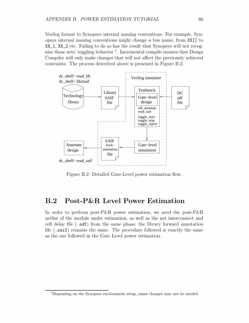
APPENDIX B. POWER ESTIMATION TUTORIAL 66
Verilog format to Synopsys internal naming conventions. For example, Syn-opsys internal naming conventions might change a bus name, from XX[] toXX_1, XX_2 etc. Failing to do so has the result that Synopsys will not recog-nise those nets’ toggling behavior 1. Incremental compile ensures that DesignCompiler will only make changes that will not affect the previously achievedcontraints. The process described above is presened in Figure B.2.
toggle_report
LibrarySAIFfile file
DCsdf
Annotate Gate−levelsimulation
dc_shell> read_saif
SAIF
filedesign
back−annotation
Gate−level
dc_shell> lib2saifdc_shell> read_lib
Technology
library
Testbench
design
Verilog simulator
sdf_annotateread_saif
toggle_starttoggle_stop
Figure B.2: Detailed Gate-Level power estimation flow.
B.2 Post-P&R Level Power Estimation
In order to perform post-P&R power estimation, we need the post-P&Rnetlist of the module under estimation, as well as the net interconnect andcell delay file (.sdf) from the same phase; the library forward annotationfile (.saif) remains the same. The procedure followed is exactly the sameas the one followed in the Gate Level power estimation.
1Depending on the Synopsys environment setup, name changes may not be needed.

Appendix C
Cadence Encounter Tutorialand Scripts
As mentioned in chapter 4, P&R was carried out in the Cadence Encounterenvironment. The tool is very memory-consuming, especially in the case oflarge designs 1. In the following sections, we provide a quick tutorial on theusage of the tool, accompanied by conclusions drawn during the P&R phaseof the switch design.
C.1 Setting the Environment
Cadence Encounter is run with the command encounter, after an includescript is executed. The tool is operated in two modes, command line andgraphics. The first is used to output the tool’s results after each operation;those results are also written in log files (extension .logXX , were X is a fileserial number), whereas the commands executed are appended in commandfiles (extension .cmdXX). The graphics mode is used to offer the freedom tothe designer to observe the placed and routed design and physicaly alter it.
Before running the tool, it is crucial to have a concrete directory organi-zation. This is due to the large number of different types of files needed toimport and use during the P&R phase. These directories are:
• /lef, with the layout header and technology files. Layout files containthe real physical layout of all standard cells of the technology library.
• /lib, with the technology library file. This directory contains the elec-trical characteristics (capacitance, timing) of all the standard cells.
• /tlf, with the timing library files of black boxes. When black boxes,like memories, are used in the design, it is usual to describe their timingcharacteristics by using such tlf files; lib files can be used instead.
1For example, in order to fully P&R in tight space constraints a 32-crosspoint switchcolumn, along with its output scheduler, time consumed was almost 8 hours.
67

APPENDIX C. CADENCE ENCOUNTER TUTORIAL AND SCRIPTS68
• /verilog, with the verilog descriptions. This directory contains: (a)the interfaces of all standard cells and/or black boxes; (b) the HDLGate-Level netlist of the design, which is written by the synthesis tool.This HDL file must be uniquified by running the Encounter commanduniquifyNetlist. Unification simply changes multi-instantiated mod-ule names into discreet ones.
• /save, where Encounter will save the design after each phase of itsexecution. A rule of thumb is: (a) to save the whole design after eachphase is complete; (b) the name of the saved file and directory shouldbe design_name_AFTER_phase_name, where phase_name is a discreetname for the phase that has just completed, like TRIAL_ROUTE.
The last two other files needed are related to the circuit clock(s): (a)the .sdc file contains the clock net names and their frequencies; (b) the.clockspec file refers to the first and also informs the tool about the elec-trical characteristics of the clock net and of the buffers that the tool may usewhen creating the clock tree. The .clockspec file is the only file importedat a later stage. All other files must be imported during the initial stage ofthe P&R process (Design Import phase).
C.2 Placement & Routing Stages
In this section we will present the exact flow followed during the P&R processand also provide the reader with useful advices. In Figure C.1 we can see achip core, along with the most often used terms in this short tutorial.
C.2.1 Design Import
As mentioned earlier, in this stage all files needed by the tool are loaded intomemory. The tool loads the standard cell library and the design in memory,as well as performs initial checks on the design. Obvious mistakes that havenot been corrected during the synthesis stage are reported during this phase.
C.2.2 Floorplaning & Pin Assignment
During this phase the design is floorplaned; this means specifying the exactsize of the chip core and the width of the power ring, putting certain blackboxes into certain locations etc. Initially, the designer has to decide upon thesize of the core, its utilization and the power ring width. The core dimensionscan be either explicitly stated, that is to give the exact dimensions of therectangle, or given by a row utilization number. In the latter case, the coreremains square and the utilization percentage defines its exact size. Rowutilization is entered as a percentage and determines the amount of unusedrow space that will be put between adjacent rows. This space will be later

APPENDIX C. CADENCE ENCOUNTER TUTORIAL AND SCRIPTS69
cell rows
������������������
������������������ ������������������������������������������
������
����
������������������������
��������������������
� � � � � � � �
��������������������
����������������������������
��������������������
������������
������������
�������������������������
�������������������������
������������������������������������������������������������
������������������������������������������������������������
stripes
ringpower
blackbox
ring/haloblock power
standard cells(registers, gates)
chip core
standard
Figure C.1: Chip Overview: Chip core, rows, power ring, power stripes, blackboxes and standard cells are visible; routing is omitted.
used for wiring. Should the designer decide to use the second approach inorder to define the core size, care should be taken in case the design has alot of “wiring”, as is the case with switches. In that case, a row utilizationof 50% seems enough; in other cases, usual utilization figures are in the areaof 70%.
Floorplaning also involves setting the width of the power ring. The powerring is made of two parallel metals, one of which carries the power, while theother acts as the ground. The power rings should be wide enough to be ableto feed the whole circuit with power. In cases of large chips, power/groundstripes should also be included. These traverse the chip in horizontal orvertical parallel lines at certain distances from each other.
When black boxes are included, care must be taken. The designer usu-ally wishes to place them at certain positions inside the core, so the toolprovides this freedom. Those black boxes have to be connected to the chip’spower/ground lines and must be surrounded by a very narrow power ringthemselves. This is because the power lines which will be at the top andbottom of each cell row need to be terminated and the black boxes wouldobscur them from reaching the other end of the core. Last of all, black boxesmust be surrounded by a “block halo”, on top of their power rings, which

APPENDIX C. CADENCE ENCOUNTER TUTORIAL AND SCRIPTS70
will prevent standard cells from being placed too close to them.Pin assignment should also be carried out in this phase. This is accom-
plished through an Encounter embedded application, called “Pin Editor”.Although the Graphical User Interface (GUI) of the application is staight-forward, care should be taken in the assignment: before it starts, “groupbus” should be enabled, in order to make the assignment easier. Also, itwas noted that, although we chose to place some pins on the north, or east,or west sides of the chip, the application put them all on the south side.This bug is overcome by re-placing the wrongfully placed pins. Note thatthe “preplace pin” opion must be always selected, as in the opposite case thepins are not fixed and it was noticed that sometimes the tool moved the pinsto other sides of the chip during the later stages. After pin assignment iscomplete, it must be saved with the command
saveIoFile XX.io
where XX.io is the pin assignment file and then immediately loaded with thecommand
loadIoFile XX.io
in order to prevent the tool from “forgetting” the assignment. After the pinassignment is saved, it can be loaded from the beginning of the design process,along with the other design files (“setting the environment phase”); as aresult, concurrent P&R attempts will do not require new pin assignments.
C.2.3 Medium Effort Placement
After the design is flooplaned, an initial placement of cells and/or black boxeshas to be performed. This task is carried out automatically by Encounterand provides the designer with the initial results of the P&R process, whichmust always be taken into account. The tool reports initial net length, whichincludes the length of all wires connecting the placed standard cells and triesto improve this result, by running the medium effort placement algorithm forabout 15 times. If the design fits into the area provided by the floorplaningphase, medium effort placement is successful; otherwise the tool will informthe designer about the violations. Another form of violation is the “blackbox” one, and is created when a black box is wrongfully placed by the designeroutside the chip borders, or when the block halo does not exist and standardcells are located too close to the black box. Medium effort floorplaning isrun with the Encounter shell command
amoebaPlace
while placement can be checked with the command
checkplace

APPENDIX C. CADENCE ENCOUNTER TUTORIAL AND SCRIPTS71
A possible medium effort report might look like the following text:
<CMD> amoebaPlace
Extracting standard cell pins and blockage ......
Pin and blockage extraction finished
Extracting macro/IO cell pins and blockage ......
Pin and blockage extraction finished
*** Starting "Amoeba(TM) placement v0.254.2.15 (mem=244.1M)" ...
Options: gp=mq-medium dp=medium
Options: congestDrivenI75 congestDrivenQ congestDrivenR1
*info: there are 2 cells with cell padding / block halo
#std cell=47808 #block=2 (0 floating + 2 preplaced) #ioInst=0 #net=52033 #term=156067 #term/net=3.00, #fixedIo=2624, #floatIo=0, #fixedPin=2368,
#floatPin=1
Total std cell len = 237.4733 (mm), area = 1.4628 (mm^2)
*info: identify 1 tech site => 1 tech site pattern
*info: estimated cell pwr/gnd rail width = 0.770 um
*info: average module density = 0.024
*info: AmoebaPlace has switched to wireLength driven mode for this low density design.
*info: density for module ’crs_pes_col_inst’ = 0.024
= stdcell_area 359808 (1462835 mu^2) / alloc_area 14715214 (59826174 mu^2).
*info: density for the rest of the design = 0.000
= stdcell_area 0 (0 mu^2) / alloc_area 12975183 (52751904 mu^2).
*info: identify 96 spare/floating instances which are grouped into 96 clusters.
*info: fixed term percentage = 5.906%
*info: fixed term center of gravity = (9751152 6169775) in coreBox (100320 100240, 35100320 19100240)
*info: partition deviation = 0.770
0|: Est. net length = 1.806e+08 (7.48e+07 1.06e+08) cpu=0:02:24 mem=890.3M
1-: Est. net length = 1.132e+08 (7.41e+07 3.91e+07) cpu=0:00:14.9 mem=890.3M
2|: Est. net length = 1.029e+08 (6.39e+07 3.91e+07) cpu=0:01:15 mem=890.3M
3-: Est. net length = 8.440e+07 (6.12e+07 2.32e+07) cpu=0:00:33.4 mem=890.3M
4|: Est. net length = 7.671e+07 (5.35e+07 2.32e+07) cpu=0:01:17 mem=890.3M
5-: Est. net length = 7.283e+07 (5.33e+07 1.95e+07) cpu=0:00:33.1 mem=890.3M
6|: Est. net length = 7.052e+07 (5.10e+07 1.95e+07) cpu=0:01:03 mem=890.3M
7-: Est. net length = 7.104e+07 (5.06e+07 2.04e+07) cpu=0:01:01 mem=890.3M
8|: Est. net length = 6.956e+07 (4.92e+07 2.04e+07) cpu=0:01:01 mem=890.3M
9-: Est. net length = 6.720e+07 (4.76e+07 1.96e+07) cpu=0:00:54.4 mem=890.3M
10|: Est. net length = 6.656e+07 (4.70e+07 1.96e+07) cpu=0:00:36.4 mem=890.3M
11-: Est. net length = 6.512e+07 (4.53e+07 1.98e+07) cpu=0:01:43 mem=906.6M
12|: Est. net length = 6.515e+07 (4.49e+07 2.02e+07) cpu=0:03:11 mem=916.1M
13-: Est. net length = 6.537e+07 (4.51e+07 2.02e+07) cpu=0:03:41 mem=931.2M
14|: Est. net length = 6.555e+07 (4.50e+07 2.05e+07) cpu=0:03:06 mem=952.0M
..+: Est. net length = 6.761e+07 (4.76e+07 2.00e+07) cpu=0:05:01 mem=1054.9M
*** cost = 6.761e+07 (4.76e+07 2.00e+07) (cpu for global=0:27:35) ***
*info: there are 2 cells with cell padding / block halo
Options: gp=mq-medium wireLengthDriven dp=medium
Starting fine tune place ...
CPU Time for Phases I and II = 0:00:21.8, Real Time = 0:00:22.0
Statistics of distance of Instance movement in detailed placement
maximum (X+Y) = 137.50 um
inst (crs_pes_col_inst/crs_32x32_RR_4/RR_pe_cr/PEnfAll/U52) with max move: (35087.6, 18075.1) -> (34956.2, 18069)
mean (X+Y) = 12.23 um
*** cpu=0:00:34.6 mem=1054.9M ***
Total net length = 5.992e+07 (4.238e+07 1.754e+07) (ext = 3.254e+07)
*** End placement (cpu=0:37:49, real=0:38:01, mem=1054.9M) ***
<CMD> checkPlace
*info: there are 2 cells with cell padding / block halo
Options: gp=mq-medium dp=medium
Check Place(new) starts ...
** Info: Total stdCell area is 5.535816e+08.
** Info: Total core area is 6.650000e+08.
** Info: Density is 8.324535e-01.
** Info: Placed = 47810
** Info: Unplaced = 0
We can see that the placement algorithm tries to fit all standard cellsand/or black boxes into the specified core area, while keeping net length toa minimum, in order to minimize possible timing violations in later stages.
C.2.4 Trial Routing
Trial routing is carried out next. During trial routing, Encounter routes thenets of the design and tries to minimize their length, or minimize the chip viausage (vias add a lot to signal delays). From the trial route report, we cansee whether the the design is routable or not. If the nets are routed too closeto each other, crosstalk interference is introduced, and the tool reports thisviolation in a “congestion distribution” table (the “-” lines refer to violated
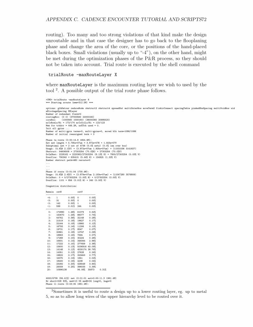
APPENDIX C. CADENCE ENCOUNTER TUTORIAL AND SCRIPTS72
routing). Too many and too strong violations of that kind make the designunroutable and in that case the designer has to go back to the flooplaningphase and change the area of the core, or the positions of the hand-placedblack boxes. Small violations (usually up to “-4”), on the other hand, mightbe met during the optimization phases of the P&R process, so they shouldnot be taken into account. Trial route is executed by the shell command
trialRoute -maxRouteLayer X
where maxRouteLayer is the maximum routing layer we wish to used by thetool 2. A possible output of the trial route phase follows.
<CMD> trialRoute -maxRouteLayer 6
*** Starting xroute (mem=312.5M) ***
options: glbDetour reduceNode obstruct2 obstruct4 spreadOut multiOuterRow moveTermZ fixAirConnect spacingTable pinAndObsSpacing multiVoidRow wid
eBlockageSpacing MSLayer
Number of redundant fterm=0
routingBox: (0 0) (37000560 22000160)
coreBox: (1000560 1000160) (36000360 20995520)
nrIoRowLo/Hi = 173/174 nrIoColLo/Hi = 123/123
Mem for trkArr = 446.2M, nrETrk used = 0.
Init all gpins ...
Number of multi-gpin terms=0, multi-gpins=0, moved blk term=1086/1086
Number of initial reassigned term = 0
Phase 1a route (0:00:14.8 1654.4M):
Est net length = 5.795e+07um = 3.872e+07H + 1.923e+07V
Suboptimal net = 2 out of 4738 (0.0% nets) (0.0% len over box)
Usage: (4.6%H 2.1%V) = (3.872e+07um 1.925e+07um) = (11531036 3141827)
Obstruct: 54606508 = 27303254 (70.0%H) + 27303254 (70.0%V)
OvInObst: 2228162 = 2220362/27303254 (8.13% H) + 7800/27303254 (0.03% V)
Overflow: 790340 = 635415 (5.44% H) + 154925 (1.33% V)
Number obstruct path=480 reroute=0
...
...
...
Phase 1f route (0:01:04 1730.4M):
Usage: (4.6%H 2.4%V) = (3.879e+07um 2.193e+07um) = (11547280 3576809)
OvInObst: 0 = 0/27303254 (0.00% H) + 0/27303254 (0.00% V)
Overflow: 1101 = 856 (0.01% H) + 245 (0.00% V)
Congestion distribution:
Remain cntH cntV
--------------------------------------
-4: 1 0.00% 0 0.00%
-3: 31 0.00% 0 0.00%
-2: 142 0.00% 1 0.00%
-1: 599 0.01% 244 0.00%
--------------------------------------
0: 172990 1.48% 61079 0.52%
1: 150670 1.29% 86077 0.74%
2: 44762 0.38% 32148 0.28%
3: 21519 0.18% 19627 0.17%
4: 22164 0.19% 13860 0.12%
5: 16793 0.14% 11306 0.10%
6: 19731 0.17% 8547 0.07%
7: 20861 0.18% 10747 0.09%
8: 18863 0.16% 7694 0.07%
9: 17268 0.15% 30224 0.26%
10: 16931 0.14% 346064 2.96%
11: 17222 0.15% 277659 2.38%
12: 15600 0.13% 5036916 43.09%
13: 14148 0.12% 4530174 38.76%
14: 14351 0.12% 27628 0.24%
15: 19822 0.17% 323453 2.77%
16: 16375 0.14% 1841 0.02%
17: 18400 0.16% 4238 0.04%
18: 23292 0.20% 426549 3.65%
19: 29309 0.25% 396033 3.39%
20: 10996138 94.08% 35873 0.31%
4000/4739 (84.41%) net (0:01:01 est=0:00:11.3 1961.4M)
Nr short=228 83%, med=13 5% medR=34 long=0, huge=0
Phase 1l route (0:03:05 1961.4M):
2Sometimes it is useful to route a design up to a lower routing layer, eg. up to metal5, so as to allow long wires of the upper hierarchy level to be routed over it.

APPENDIX C. CADENCE ENCOUNTER TUTORIAL AND SCRIPTS73
Number of deextended terms = 1086
Prep phase2 (0:00:00.0 1961.4M):
...
...
...
*** Completed Phase 1 route (0:35:35 1961.4M) ***
Phase 2a route (0:01:49 1961.4M)
Phase 2b route (0:01:45 1961.4M)
Total length: 6.070e+07um, number of vias: 23989
M1(H) length: 7.300e+00um, number of vias: 7
M2(V) length: 6.764e+06um, number of vias: 2925
M3(H) length: 1.833e+07um, number of vias: 5829
M4(V) length: 1.099e+07um, number of vias: 9178
M5(H) length: 2.046e+07um, number of vias: 6050
M6(V) length: 4.159e+06um
*** Completed Phase 2 route (0:03:34 1961.4M) ***
*** xroute (cpu=0:39:09 mem=1961.4M) ***
<CMD> saveDesign /proj/carv/users/simos/unix/MSc/bufXbar32x32/SOC_ENCOUNTER/bx_top/save/bx_top_AFTER_TRIAL_ROUTE.enc
*** Completed saveRoute (cpu=0:00:07.6 real=0:00:09.0 mem=1961.4M) ***
We can see the congestion distribution table, with minor horizontal andvertical violations; experience showed that such small violations can be min-imized in later phases. Trial routing involves two phases, and each phaseconsists of many sub-phases; each phase tries to minimize congestion vio-lations, obstructions and overflows. Especially phase 1.f shows the biggestchanges, compared to the improvements achieved between other concurrentphases. If the design still includes large distribution violations after thatphase, it is certainly unroutable 3 .
C.2.5 Clock Tree Synthesis
The clock nets are by far the most important ones in a synchronous design;hence, they are routed separately in the clock tree synthesis phase. Of course,clock nets must be buffered inside the chip as evenly as possible, in order toavoid clock skew (uncertainty - see Figure C.2).
The .clockspec file is included during this phase, so the tool knows whichtypes of buffers to use when producing the clock tree. Obviously, space mustbe left inside the core, in order to place those buffers, so floorplaning shouldnot “stress” the core area. The tool produces full reports of the clock treedepth and of the final clock skew. Clock tree synthesis is performed by thefollowing commands: first we have to specify the clock specification file,
specifyClockTree -clkFile XX.clockspec
Next we create the clock save directory, with the command
createSaveDir dir_name
Clock checks are then performed by running
checkUnique
3Note that routing violations are visible in the Encounter graphics mode, but thedesigner must have selected that option.

APPENDIX C. CADENCE ENCOUNTER TUTORIAL AND SCRIPTS74
registersclock pin
clock tree
circuit
Figure C.2: Clock Tree Example
Last of all, the actual clock synthesis procedure is executed, with the com-mand
ckSynthesis -rguide dir_name/XX.guide -report dir_name/XX.ctsrpt
where XX.guide and XX.ctsrpt are internal Encounter files 4
A sample output of the clock synthesis, though inevitably “cut” due tospace limitations, can be seen in the following text.
<CMD> specifyClockTree -clkfile xp_col_rd.clockspec
specifyClockTree Option : -clkfile xp_col_rd.clockspec
RouteType : FE_CTS_DEFAULT
PreferredExtraSpace : 1
Shield : NONE
PreferLayer : M2 M3
Avg. Cap : 0.157351 (ff/um) [0.000157351]
Avg. Res : 0.221429(ohm/um) [0.000221429]
M1 w=0.24(um) s=0.24(um) p=0.56(um) es=0.88(um) cap=0.146(ff/um) res=0.321(ohm/um)
M2 w=0.28(um) s=0.28(um) p=0.66(um) es=1.04(um) cap=0.153(ff/um) res=0.221(ohm/um)
M3 w=0.28(um) s=0.28(um) p=0.56(um) es=0.84(um) cap=0.162(ff/um) res=0.221(ohm/um)
M4 w=0.28(um) s=0.28(um) p=0.66(um) es=1.04(um) cap=0.153(ff/um) res=0.221(ohm/um)
M5 w=0.28(um) s=0.28(um) p=0.56(um) es=0.84(um) cap=0.162(ff/um) res=0.221(ohm/um)
M6 w=0.44(um) s=0.44(um) p=1.32(um) es=2.2(um) cap=0.129(ff/um) res=0.0932(ohm/um)
...
...
...
********** Clock clk_wr Pre-Route Timing Analysis **********
Nr. of Subtrees : 1
Nr. of Sinks : 2
Nr. of Buffer : 44
Nr. of Level (including gates) : 39
Max trig. edge delay at sink(R): xp_hier_col_2_inst/clk_wr 4992.4(ps)
Min trig. edge delay at sink(R): xp_hier_col_1_inst/clk_wr 4989.4(ps)
(Actual) (Required)
Rise Phase Delay : 4989.4~4992.4(ps) 0~5000(ps)
Fall Phase Delay : 5600.1~5679.3(ps) 0~5000(ps)
Trig. Edge Skew : 3(ps) 500(ps)
Rise Skew : 3(ps)
Fall Skew : 79.2(ps)
Max. Rise Buffer Tran. : 482.6(ps) 500(ps)
4Due to the large number of commands that must be executed, clock tree synthesis ismore prefferably run from the Enounter graphics mode.
APPENDIX C. CADENCE ENCOUNTER TUTORIAL AND SCRIPTS75
Max. Fall Buffer Tran. : 471.7(ps) 500(ps)
Max. Rise Sink Tran. : 900.2(ps) 500(ps)
Max. Fall Sink Tran. : 628.5(ps) 500(ps)
Generating Clock Analysis Report bx_top_cts/bx_top_cts.ctsrpt ....
Generating Clock Routing Guide bx_top_cts/bx_top_cts.guide ....
Clock Analysis (CPU Time 0:00:00.2)
<CMD> saveClockNets -output bx_top_cts/bx_top_cts.ctsntf
<CMD> saveNetlist bx_top_cts/bx_top_cts.v
Writing Netlist "bx_top_cts/bx_top_cts.v" ...
<CMD> savePlace bx_top_cts/bx_top_cts.place
<CMD> saveDesign /proj/carv/users/simos/unix/MSc/bufXbar32x32/SOC_ENCOUNTER/bx_top/save/bx_top_AFTER_CLK_SYN.enc
C.2.6 Timing Driven Placement
After the clock tree is placed and routed, the placement stage is re-run, butin a high-effort, timing driven mode. This allows the tool to possibly movesome standard cells to new positions, in order to achieve timing goals. Anexample output of this process is shown below. We can see that, in this case,the tool has actually moved some cells.
<CMD> amoebaPlace
*** Starting "Amoeba(TM) placement v0.254.2.15 (mem=241.3M)" ...
Options: gp=mq-medium dp=medium
Options: congestDrivenI75 congestDrivenQ congestDrivenR1
...
...
...
Starting fine tune place ...
CPU Time for Phases I and II = 0:00:22.6, Real Time = 0:00:23.0
Statistics of distance of Instance movement in detailed placement
maximum (X+Y) = 162.36 um
inst (crs_pes_col_inst/crs_32x32_RR_24/cr_choose_reg_1) with max move: (761.64, 17791.8) -> (617.76, 17773.3)
mean (X+Y) = 18.84 um
*** cpu=0:00:35.9 mem=1052.0M ***
Total net length = 4.134e+07 (3.025e+07 1.109e+07) (ext = 1.223e+07)
*** End placement (cpu=0:38:31, real=0:39:33, mem=1052.0M) ***
...
C.2.7 Timing Driven Final and Global Route
This is the last main phase of the P&R process. In this phase, the tool routesonce more the design and tries to use the minimum net length and numberof vias, choose the appropriate metal layer for each net, and possibly addbuffers or resize cells, in order to achieve unmet timing constraints. 5 Thedesigner can choose which final router the tool is going to use: WRoute orNanoRoute. The latter is a new router and is actually suggested by Cadence,as it is considered to be faster and better, although the author has observedthat WRoute has provided better results in some cases; hence, possibly bothmust be tried. A limited output of the NanoRoute final router, along withthe commands executed, can be seen below 6:
5It is reminded that the time t needed to load a wire equals t = C∆V /I , where C isthe wire’s capacitance, ∆V the voltage drop/increase and I the current flowing throughthe wire. Hence, for the same ∆V , time is reduced if (a) we allow more current to flowthrough the wire, as a result the wire must be wider, in order to have small resistance; (b)load capacitance is small; this can be achieved by buffering the net.
6Due to the large number of commands that must be executed, we suggest to runNanoRoute in the Enounter graphics mode, than in the command line interface.

APPENDIX C. CADENCE ENCOUNTER TUTORIAL AND SCRIPTS76
<CMD> getNanoRouteMode -quiet routeSiEffort
<CMD> getNanoRouteMode -quiet
<CMD> setNanoRouteMode -quiet drouteFixAntenna true
<CMD> setNanoRouteMode -quiet routeInsertAntennaDiode false
<CMD> setNanoRouteMode -quiet routeAntennaCellName default
<CMD> setNanoRouteMode -quiet routeWithTimingDriven true
<CMD> setNanoRouteMode -quiet routeWithTimingOpt true
<CMD> setNanoRouteMode -quiet optimizeBi true
<CMD> setNanoRouteMode -quiet optimizeGs true
<CMD> setNanoRouteMode -quiet optimizeFixSetupTime true
<CMD> setNanoRouteMode -quiet optimizeTargetSetupSlack 0.000000
<CMD> setNanoRouteMode -quiet optimizeFixMaxCap false
<CMD> setNanoRouteMode -quiet optimizeFixHoldTime false
<CMD> setNanoRouteMode -quiet optimizeTargetHoldSlack 0.000000
<CMD> setNanoRouteMode -quiet optimizeFixMaxTran false
<CMD> setNanoRouteMode -quiet optimizeDontUseCellFile default
<CMD> setNanoRouteMode -quiet routeWithSiDriven false
<CMD> setNanoRouteMode -quiet routeSiEffort min
<CMD> setNanoRouteMode -quiet siNoiseCTotalThreshold 0.050000
<CMD> setNanoRouteMode -quiet siNoiseCouplingCapThreshold 0.005000
<CMD> setNanoRouteMode -quiet routeWithSiPostRouteFix false
<CMD> setNanoRouteMode -quiet drouteAutoStop true
<CMD> setNanoRouteMode -quiet routeSelectedNetOnly false
<CMD> setNanoRouteMode -quiet routeFixPrewire false
<CMD> setNanoRouteMode -quiet drouteStartIteration default
<CMD> setNanoRouteMode -quiet envNumberProcessor 1
<CMD> setNanoRouteMode -quiet routeTopRoutingLayer default
<CMD> setNanoRouteMode -quiet drouteEndIteration default
<CMD> deleteSwitchingWindows
<CMD> cleanupDetailRC
<CMD> globalDetailRoute
globalDetailRoute
...
...
...
WRoute is run with the command
wroute -timingDriven
WRoute and NanoRoute perform Physically Knowledgable Synthesis - PKS,that is, they both try to optimize design timing by actually changing somestandard cells (cell resizing), or adding buffers to nets, while having in mindthe actual physical layout of the design. Usually, after many optimizationattempts, the algorithm finishes and reports the “worst” path in therms oftiming. A possible report of that kind is shown below:
+-----------------------------------------+
| Report | report_timing |
|------------------+----------------------|
| Options | |
+------------------+----------------------+
| Date | 20040417.162148 |
| Tool | pks_shell |
| Release | v5.9-s043 |
| Version | Apr 18 2003 19:47:51 |
+------------------+----------------------+
| Module | crs_pes_col |
| Timing | LATE |
| Slew Propagation | WORST |
| PVT Mode | max |
| Tree Type | worst_case |
| Process | 1.00 |
| Voltage | 1.98 |
| Temperature | 0.00 |
| time unit | 1.00 ns |
| capacitance unit | 1.00 pF |
| resistance unit | 1.00 kOhm |
+-----------------------------------------+
Path 1: MET Setup Check with Pin crs_32x32_RR_32/cr_choose_reg_4/CK
Endpoint: crs_32x32_RR_32/cr_choose_reg_4/SE (^) checked with leading edge of ’clk_rd’
Beginpoint: crs_32x32_RR_32/cr_change_32_reg/Q (^) triggered by leading edge of ’clk_rd’
Other End Arrival Time 9.24
- Setup 0.11
+ Phase Shift 3.35
= Required Time 12.48
- Arrival Time 12.03
= Slack Time 0.45
Clock Rise Edge 0.00
+ Drive Adjustment 4.11

APPENDIX C. CADENCE ENCOUNTER TUTORIAL AND SCRIPTS77
= Beginpoint Arrival Time 4.11
+---------------------------------------------------------------------------------------------------------------+
| Instance | Arc | Cell | Delay | Arrival | Required |
| | | | | Time | Time |
|---------------------------------------+---------------+--------------------------+-------+---------+----------|
| | clk_rd ^ | | | 4.11 | 4.56 |
| clk_rd__L1_I0 | A ^ -> Z ^ | BUFD16 | 2.49 | 6.60 | 7.06 |
| clk_rd__L2_I0 | A ^ -> Z ^ | BUFD16 | 1.01 | 7.61 | 8.07 |
| clk_rd__L3_I0 | A ^ -> Z ^ | BUFD16 | 0.15 | 7.76 | 8.21 |
| clk_rd__L4_I0 | A ^ -> Z ^ | BUFD16 | 0.10 | 7.86 | 8.31 |
| clk_rd__L5_I0 | A ^ -> Z ^ | BUFD16 | 0.21 | 8.07 | 8.52 |
| clk_rd__L6_I0 | A ^ -> Z ^ | BUFD16 | 0.39 | 8.46 | 8.91 |
| clk_rd__L7_I13 | A ^ -> Z ^ | BUFD16 | 0.63 | 9.09 | 9.54 |
| crs_32x32_RR_32 | clk_rd ^ | cr_sched_32x32_RR_SPC_31 | | 9.09 | 9.54 |
| crs_32x32_RR_32/cr_change_32_reg | CK ^ -> Q ^ | DFEPQ2 | 0.46 | 9.55 | 10.01 |
| crs_32x32_RR_32/RR_pe_cr | In[0] ^ | RR_prior_enf_cs_SPC_31 | | 9.55 | 10.01 |
| crs_32x32_RR_32/RR_pe_cr/U3 | A1 ^ -> Z ^ | NOR2M1D2 | 0.16 | 9.71 | 10.16 |
| crs_32x32_RR_32/RR_pe_cr/PEnfPar | In[0] ^ | CRS_0_SPC_31 | | 9.71 | 10.16 |
| crs_32x32_RR_32/RR_pe_cr/PEnfPar/U95 | A4 ^ -> Z v | NOR4M1D2 | 0.04 | 9.75 | 10.20 |
| crs_32x32_RR_32/RR_pe_cr/PEnfPar/U90 | A2 v -> Z ^ | NOR4D4 | 0.19 | 9.94 | 10.39 |
| crs_32x32_RR_32/RR_pe_cr/PEnfPar/U14 | A4 ^ -> Z v | NAN4M2D1 | 0.15 | 10.09 | 10.54 |
| crs_32x32_RR_32/RR_pe_cr/PEnfPar/U47 | A v -> Z ^ | INVD2 | 0.10 | 10.18 | 10.64 |
| crs_32x32_RR_32/RR_pe_cr/PEnfPar/U83 | A2 ^ -> Z v | NAN2D1 | 0.07 | 10.26 | 10.71 |
| crs_32x32_RR_32/RR_pe_cr/PEnfPar/U81 | A3 v -> Z ^ | NAN4M2D2 | 0.08 | 10.33 | 10.79 |
| crs_32x32_RR_32/RR_pe_cr/PEnfPar/U85 | A2 ^ -> Z v | NOR2D2 | 0.08 | 10.41 | 10.87 |
| crs_32x32_RR_32/RR_pe_cr/PEnfPar/U92 | A4 v -> Z ^ | NAN4M2D2 | 0.06 | 10.47 | 10.93 |
| crs_32x32_RR_32/RR_pe_cr/PEnfPar/U21 | A4 ^ -> Z v | NAN4M1D2 | 0.08 | 10.55 | 11.01 |
| crs_32x32_RR_32/RR_pe_cr/PEnfPar/U87 | A1 v -> Z ^ | NOR4D1 | 0.12 | 10.68 | 11.13 |
| crs_32x32_RR_32/RR_pe_cr/PEnfPar/U69 | A2 ^ -> Z ^ | AND2D2 | 0.15 | 10.83 | 11.28 |
| crs_32x32_RR_32/RR_pe_cr/PEnfPar/U38 | A ^ -> Z v | INVD1 | 0.08 | 10.91 | 11.36 |
| crs_32x32_RR_32/RR_pe_cr/PEnfPar/U74 | A3 v -> Z ^ | NOR4D2 | 0.13 | 11.04 | 11.49 |
| crs_32x32_RR_32/RR_pe_cr/PEnfPar/U73 | A2 ^ -> Z v | NAN2D2 | 0.08 | 11.12 | 11.57 |
| crs_32x32_RR_32/RR_pe_cr/PEnfPar/U15 | A3 v -> Z ^ | NOR3M1D2 | 0.12 | 11.24 | 11.70 |
| crs_32x32_RR_32/RR_pe_cr/PEnfPar/U116 | A3 ^ -> Z v | NAN3M1D2 | 0.10 | 11.34 | 11.79 |
| crs_32x32_RR_32/RR_pe_cr/PEnfPar/U11 | A3 v -> Z v | OR4D1 | 0.24 | 11.58 | 12.03 |
| crs_32x32_RR_32/RR_pe_cr/PEnfPar | OneDetected v | CRS_0_SPC_31 | | 11.58 | 12.03 |
| crs_32x32_RR_32/RR_pe_cr/U65 | A v -> Z v | BUFD20 | 0.13 | 11.71 | 12.16 |
| crs_32x32_RR_32/RR_pe_cr/U24 | SL v -> Z ^ | MUX2DL | 0.32 | 12.03 | 12.48 |
| crs_32x32_RR_32/RR_pe_cr | Out[4] ^ | RR_prior_enf_cs_SPC_31 | | 12.03 | 12.48 |
| crs_32x32_RR_32/cr_choose_reg_4 | SE ^ | SDFPQ1 | 0.00 | 12.03 | 12.48 |
+---------------------------------------------------------------------------------------------------------------+
Timing driven total CPU time = 620.930000 seconds. <PLC-530>.
Info: Writing "/dev/null" ... <PLC-601>.
Info: Written out 582720 gcells for 6 layers <PLC-601>.
Info: End routability analysis: cpu: 0:12:30, real: 0:12:38, peak: 387.36 megs. <PLC-601>.
...
...
...
Begin antenna checking ...
Layer H-Length V-Length Down-Via Violation ( Antenna)
---------------------------------------------------------------------
1st routing 189230 987 0 0 ( 0)
2nd routing 7714 918427 235465 0 ( 0)
3rd routing 1906908 366 128602 0 ( 0)
4th routing 150 195163 46695 0 ( 0)
5th routing 410392 51 4363 0 ( 0)
6th routing 333 138479 1752 0 ( 0)
---------------------------------------------------------------------
2514730 1253475 416877 0 ( 0)
End antenna checking: cpu: 0:00:19, real: 0:00:20, peak: 94.87 megs.
End final routing: cpu: 0:17:20, real: 0:17:29, peak: 94.87 megs.
Begin DB out ...
Writing "crs_pes_col.wdb" ...
Written out 11 layers, 6 routing layers, 0 overlap layer
Written out 510 macros, 82 used
Written out 47975 components
47975 core components: 0 unplaced, 47975 placed, 0 fixed
Written out 1538 physical pins
1538 physical pins: 0 unplaced, 1538 placed, 0 fixed
Written out 49129 nets, 49033 routed
Written out 2 special nets, 2 routed
Written out 263166 terminals
Written out 232684 real and virtual terminals
End DB out: cpu: 0:00:00, real: 0:00:04, peak: 94.87 megs.
...
C.2.8 Timing Reports and Design Optimizations
Timing violations are obviously the most important ones in the whole designprocess. Therefore, Encounter is able to report design timing violations,both in pre- and post-routed clock design instances. In the first case, clockis considered to be ideal. This report is generated in the very early design

APPENDIX C. CADENCE ENCOUNTER TUTORIAL AND SCRIPTS78
stages, that is right after the trial route phase. In this way, the designer canhave a very early picture of the design’s timing violations, and thus concludeon whether it is worth continuing the P&R process, or go back to earlierstages. The same timing report can be generated after the global and finalrouting phase and provides the designer with the actual timing violations thatpossibly exist. In order to produce a timing violation report, the design mustfirst be RC extracted: at first, the designer has to define the RC extractionmodel detail, with the command
setExtractRCMode -detail/-default -reduce 5 -noise
and then RC extraction is performed with the shell command
extractRC -outfile XX.cap
where XX.cap is the capacitance information output file. A possible outputof these two commands is shown below:
RC Extraction for instance crs_pes_col
RC Database Name : crs_pes_col.rcdb.gz
Detail Parasite RC Extraction for crs_pes_col
wire [660 220 20019570 169940] IOBox[0 0 20020560 170080]
bounrary [0 0 20020560 170080]
max_track=10
**WARN: Since cap. table file was not provided, it will be created internally with the following process info:
* Layer Id : 1 - M1
Thicknesss : 0.48
Min Width : 0.24
Layer Dielectric : 4.1
* Layer Id : 2 - M2
Thicknesss : 0.58
Min Width : 0.28
Layer Dielectric : 4.1
* Layer Id : 3 - M3
Thicknesss : 0.58
Min Width : 0.28
Layer Dielectric : 4.1
* Layer Id : 4 - M4
Thicknesss : 0.58
Min Width : 0.28
Layer Dielectric : 4.1
* Layer Id : 5 - M5
Thicknesss : 0.58
Min Width : 0.28
Layer Dielectric : 4.1
* Layer Id : 6 - M6
Thicknesss : 0.86
Min Width : 0.44
Layer Dielectric : 4.1
...
...
...
Nr. Extracted Resistors : 258800
Nr. Extracted Ground Cap. : 211830
Nr. Extracted Coupling Cap. : 2001384
Detail RC Extraction Completed (CPU Time= 0:01:25 MEM= 260.6M)
RC Extraction Completed (CPU Time= 0:01:25 MEM= 260.6M)
Last of all, the actual timing model is extracted by the command
genTlfModel
whereas, after these commands are executed, timing report can be generatedwith the command
reportViolation -outfile XX.tarpt -num 50
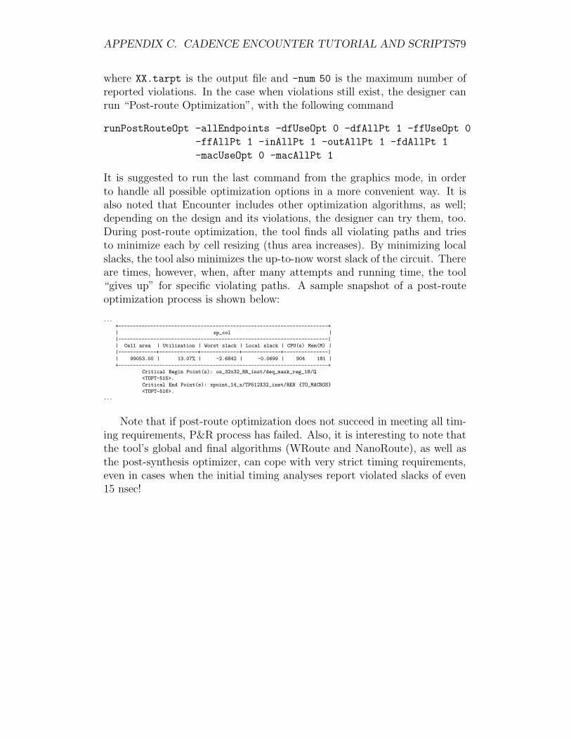
APPENDIX C. CADENCE ENCOUNTER TUTORIAL AND SCRIPTS79
where XX.tarpt is the output file and -num 50 is the maximum number ofreported violations. In the case when violations still exist, the designer canrun “Post-route Optimization”, with the following command
runPostRouteOpt -allEndpoints -dfUseOpt 0 -dfAllPt 1 -ffUseOpt 0
-ffAllPt 1 -inAllPt 1 -outAllPt 1 -fdAllPt 1
-macUseOpt 0 -macAllPt 1
It is suggested to run the last command from the graphics mode, in orderto handle all possible optimization options in a more convenient way. It isalso noted that Encounter includes other optimization algorithms, as well;depending on the design and its violations, the designer can try them, too.During post-route optimization, the tool finds all violating paths and triesto minimize each by cell resizing (thus area increases). By minimizing localslacks, the tool also minimizes the up-to-now worst slack of the circuit. Thereare times, however, when, after many attempts and running time, the tool“gives up” for specific violating paths. A sample snapshot of a post-routeoptimization process is shown below:
...
+-----------------------------------------------------------------------+
| xp_col |
|-----------------------------------------------------------------------|
| Cell area | Utilization | Worst slack | Local slack | CPU(s) Mem(M) |
|-------------+-------------+-------------+-------------+---------------|
| 99053.00 | 13.07% | -2.6842 | -0.0699 | 904 181 |
+-----------------------------------------------------------------------+
Critical Begin Point(s): os_32x32_RR_inst/deq_mask_reg_18/Q
<TOPT-515>.
Critical End Point(s): xpoint_14_x/TP512X32_inst/REN {TO_MACROS}
<TOPT-516>.
...
Note that if post-route optimization does not succeed in meeting all tim-ing requirements, P&R process has failed. Also, it is interesting to note thatthe tool’s global and final algorithms (WRoute and NanoRoute), as well asthe post-synthesis optimizer, can cope with very strict timing requirements,even in cases when the initial timing analyses report violated slacks of even15 nsec!

Appendix D
Switch Synchronization Details
D.1 Introduction
Switches are multi-clock ASICs. This is because, if the input links are fast(i.e. more than 1 Gbit/sec), tranceiver circuits used also carry the other-endtransmitter clock; this clock is recovered by the tranceiver circuits locatedat the switch inputs (see Figure D.1). If the links are long, then the phase
LIN
E C
AR
DS
clk_s
clk_s
RCVR1
RCVR2
RCVR3
RCVR4
SWITCHCORE
clk_s
clk_s
clk1
clk2
clk3
clk4
out1
out2
out3
out4
in1
in2
in3
in4
LC1
LC2
LC3
LC4
clk1_i
clk2_i
clk3_i
clk4_i
Figure D.1: The problem of communicating across clock domains: clocks clk1to clk4 are the recovered versions of the initial line card (LC) clocks clk1 i toclk4 i. Clock recovery is carried out by the switch tranceiver circuits. Theseclocks differ from each other, due to phase variations, and they all have tobe synchronized to the switch core’s clock.
of the recovered clock, at the receiver (i.e. switch), can vary widely relativeto the phase of the transmitted clock (i.e. line card), at the other end. Thisposes metastability issues.
D.2 The Metastability Problem
Figure D.2 shows a typical positive edge flip-flop timing specification. Inputdata must be stable setup time (tSU) before the edge arrives and must remain
80
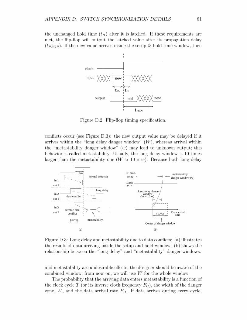
APPENDIX D. SWITCH SYNCHRONIZATION DETAILS 81
the unchanged hold time (tH) after it is latched. If these requirements aremet, the flip-flop will output the latched value after its propagation delay(tPROP ). If the new value arrives inside the setup & hold time window, then
PROP
tHtSU
new
newold
clock
input
output
t
Figure D.2: Flip-flop timing specification.
conflicts occur (see Figure D.3): the new output value may be delayed if itarrives within the “long delay danger window” (W ), whereas arrival withinthe “metastability danger window” (w) may lead to unknown output; thisbehavior is called metastability. Usually, the long delay window is 10 timeslarger than the metastability one (W ≈ 10 × w). Because both long delay
(W = 10 w)
t SU+tH
t SU+tH
in 1
out 1
in 2
out 2
t PD
data conflict
conflictterrible data
metastability
long delay
in 3
out 3
normal behavior
Clockcycle
FF prop.delay
Data arrivaltime
Center of danger window
(a) (b)
metastabilitydanger window (w)
long delay dangerwindow
Figure D.3: Long delay and metastability due to data conflicts: (a) illustratesthe results of data arriving inside the setup and hold window. (b) shows therelationship between the “long delay” and “metastability” danger windows.
and metastability are undesirable effects, the designer should be aware of thecombined window; from now on, we will use W for the whole window.
The probability that the arriving data enters metastability is a function ofthe clock cycle T (or its inverse clock frequency FC), the width of the dangerzone, W , and the data arrival rate FD. If data arrives during every cycle,
APPENDIX D. SWITCH SYNCHRONIZATION DETAILS 82
then the probability p equals p(enter metastability) = W/T = W × FC .When data arrival rate is FD, the rate R of entering metastability equalsR(entering metastability) = W×FC×FD. As an example, consider the “newpacket” notification pulse that traverses the two clock domains of the switchpresented in this work. In a 0.18µm technology, gate delay is approximately60psec and W is estimated to be approximately 90psec; clock frequency is300MHz (clock cycle 3.35nsec). If data must be synchronized every 10clock cycles (as is the worst case with the “new packet” signal), then themetastability rate equals R = W × FC × FD = 800KHz, that is, once every1.25 nsec, which is unacceptably large.
After a metastability conflict occurs: (a) the output may send the correctvalue after a long delay; or (b) the output may go to 1 or 0 in random. Inpractice, the decision time of a synchronizer is exponentially distributed [32].Thus, if a system is designed to wait a time, τ , before sampling the synchro-nizer, the probability of synchronization failure decreases exponentially as τis increased. Given metastability at t = 0, the metastability probability att > 0 is e−t/τ . A failure exists if metastability remains during the next clockcycle, too. Failure will be thus p(enter m.s.) × p(stil m.s. after T), and thecorresponding failure rate will equal
Rate(failure) = Rate(enter m.s.)×p(still m.s. after T) = W×FC×FD×e−T/τ
Mean Time Between Failure (MTBF) will then equal
MTBF = 1/Rate(failure) = eT/τ/W × FC × FD
Depending on the parameter τ , MTBF can be almost eliminated.
D.3 Synchronizer Requirements
From the above, it is evident that all recovered clocks have to be synchronizedto a common clock, clk_s. Switch outputs, on the other hand, can besynchronized to the switch core clock clk_s; this reduces outgoing latency.
There is large number of possible synchronization solutions. The decisionon which to use depends mostly on the latency requirements and the syn-chronization protocol used. Switches usually use elastic buffers at the inputs,in order to synchronize the received multi-bit information (packet data) [31].Elastic buffers are merely 2-port SRAMs with two asynchronous ports; aread and a write pointer are used to select the read and write position inthe memory array; these two pointers are synchronized to their respectiveclocks. Elastic buffers are large and complicated circuits, and require theuse of an SRAM in every synchronization boundary. The 32×32 bufferedcrossbar switch would need one such elastic buffer at each input.
But since SRAMs were inevitably used at the switch crosspoints, choos-ing to use 2-port versions would immediately solve the data synchronization

APPENDIX D. SWITCH SYNCHRONIZATION DETAILS 83
problem, without the need for elastic buffers. The only other information thathas to be synchronized is a control signal: the 1-bit “new packet” notifica-tion pulse. This signal is produced at most every minimum-size packet time,10 clock cycles. Since 1024 (32×32) such signals have to be synchronized,the synchronization circuit has to be the simplest possible. Also note thatthe various incoming clocks must have approximately the same frequency asthe switch core’s clock, as the switch incoming throughput is the same asthe outgoing one, and no speedup is required, due to the adopted architec-ture; hence the synchronizer used must be able to efficiently deal with smallfrequency and phase variations, while keeping its complexity to a minimum.
D.4 1-bit Synchronizer Design
The two flip-flop synchronizer is possibly the most efficient solution in suchpleisiochronous situations (see Figure D.4). Two flip-flops are used in order to
achnowledgment signal
bit_d0 bit_d1 bit_d2 bit_det
(synchronized to sender’sinput value
clock clk_in)
synchronizedvalue
positive edge detector
clk outreceiver’s clock
Figure D.4: The 2 flip-flop synchronizer.
allow the single-bit data a complete cycle for settling; hence, settling time is 2clock cycles, whereas synchronization latency is 3 clock cycles. We decided touse 3 flip-flops for settling, in order to be more redundant. The synchronizedsignal is driven into a positive edge detector, which eventually lathes thesignal and outputs a complete pulse. This protocol is called “4-phase”, sincea complete cycle of the incoming pulse triggers one synchronization event.

Appendix E
Power Optimization Techniques
Low power consumption has become a crucial issue in IC design. In portabledevices, low power consumption has long been considered one of the maindesign contraints. In high-performance processors, on the other hand, powerconsumption was traditionally the secondary constraining factor; however,this has changed due to the concerns on the cooling and packaging cost.What is more, the increase in power consumption has resulted in highertemperature, which in turn reduces reliability 1. Therefore, low power tech-niques are important for current and future VLSI design. In this section wewill examine theoretically various methods which, if used correctly, can de-crease a circuits’s power consumption. Some of these methods are adopted bythe Synopsys Power Compiler power optimization algorithms. The methodspresented can also be found in [25].
E.1 RTL Power Optimization
E.1.1 Glitch Minimization
A design’s structure in the RTL level can have a significant affect on inter-block glitches. This seems logical when we face a circuit’s blocks as largegates that connect to each other. Glitch propagation through these RTLblocks can affect power.
Path Balancing and Depth Reduction
Glitch can be reduced if we balance signal paths, as well as by increasingcircuit depth 2. For example, in Figure E.1 we can see two implementationsof a 4-number adder. If all inputs arrive at the same time, in the case of
1Realiability is a crucial demand in switching devices: 5 minutes/year downtime isconsidered to be a reasonable value.
2Of course, increasing the depth , increases the capacitance; on the other hand, reducingthe depth imposes the use of more registers, hence power is increased. Such tradeoffs willbe largely encountered in the following techniques as well.
84

APPENDIX E. POWER OPTIMIZATION TECHNIQUES 85
the chain adder of Figure E.1(a), adder 2 will compute twice every clockcycle and adder 3 will compute 3 times per cycle. This results in uselesstransitions that consume power. On the other hand, in the case of the treeadder of Figure E.1(b), all paths are balanced, hence glitching is minimal.
(b)
Adder 1 Adder 2
Adder 2
Adder 2
Adder 2A
B
C
D
OutAdder 3
D
C
B
AOut
(a)
Figure E.1: Path balancing and depth reduction power optimization: case(a) is an unbalanced chain adder, while (b) is a completely balanced, almostglitch free tree adder.
E.1.2 Exploitation of Resource Sharing
Resource sharing is a tradeoff between area and performance, but it canaffect power consumption as well. Usually, when we share a unit, we needmultiplexors at its inputs, which results in increased power consumption. Forexample, we can choose to use a parallel architecture (by duplicating the re-sources) in case we need a high-throughput circuit, or a time-multiplexedarchitecture for low-throughput circuits. As an example, in Figure E.2,the parallel implementation (E.2(a)) approach consumes less power than thetime-multiplexed one (E.2(b)), because the latter involves using multiplex-ors and due to the fact that the time-multiplexed approach destroys datacorrelation.
O1Adder 1
Adder 2
B
A
COut
(a)
O1
OutAdder
(b)
C
B
A
Figure E.2: Exploitation of resource sharing power optimization: case (a) isa parallel implentation, while (b) time-multiplexes input data, in order toconsume less area, but is not as power-aware as approach (a).

APPENDIX E. POWER OPTIMIZATION TECHNIQUES 86
E.1.3 Dynamic Power Management
The idea of dynamic power management is to shut down some blocks (ALUs,registers) that are not performing valuable jobs all the time. There are 4approaches to this idea.
Pre-computation
With pre-computation we compute some of the circuit outputs one or morecycles earlier, in order to decrease the switching of the combinational cir-cuit. This can be achieved by implementing predictor functions, which mustcover as many circuit states possible. This method can achieve as much as60% power savings, but with small area overhead in pipelined circuits, andis difficult to implement in sequential circuits. For example, the predictorfunctions in the case of the comparator shown in Figure E.3 are very sim-ple: If we compare the multi-bit numbers C & D, functions g1 and g2 areg1 = C[n − 1]D[n − 1]
′
for C > D, and g2 = C[n − 1]′
D[n − 1] for C < D;as a result, g1 + g2 = (C[n − 1]XORD[n − 1])
′
. For equiprobable inputs,XNOR power consumption is p(XNOR) = 0.5, so we achieve an average of50% power reduction.
XNOR
R1
R2
en
C[n−1]
D[n−1]
D[n−2]
C[0]
D[0]
C[n−2]R3
f
C > D
Figure E.3: Pre-computation power optimization: the result of the C > Dcomparison is evaluated by first comparing the most significant bits of C andD and then by comparing the rest. Power consumption savings can be asmuch as 60%.
Gated Clocks
Clock gating can be directly implemented on our code. The designer findsthe cases when a specific subcircuit must remain idle and builds an activationfunction. Gating is performed by AND-ing the real clock with the latchedoutput (in order to avoid glitches) of the activation function. Such techniquescan reduce the power consumption of FSMs by almost 30%. For testability
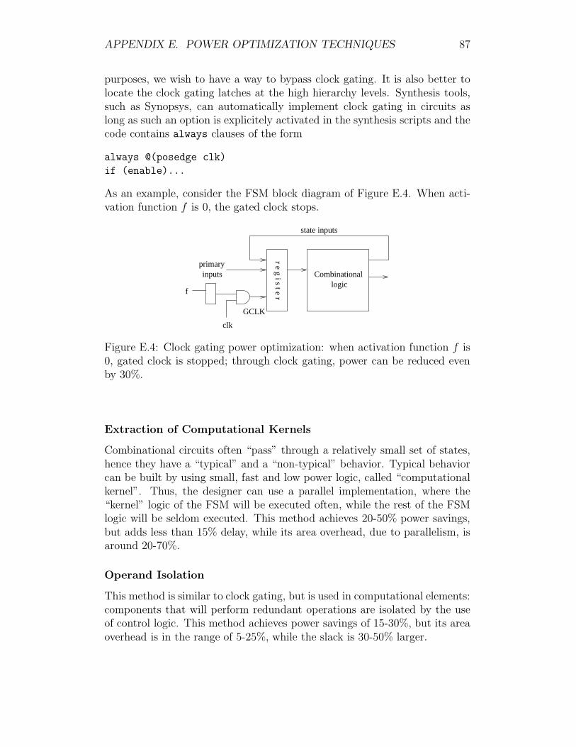
APPENDIX E. POWER OPTIMIZATION TECHNIQUES 87
purposes, we wish to have a way to bypass clock gating. It is also better tolocate the clock gating latches at the high hierarchy levels. Synthesis tools,such as Synopsys, can automatically implement clock gating in circuits aslong as such an option is explicitely activated in the synthesis scripts and thecode contains always clauses of the form
always @(posedge clk)
if (enable)...
As an example, consider the FSM block diagram of Figure E.4. When acti-vation function f is 0, the gated clock stops.
GCLK
state inputs
logicCombinationalinputs
primary
f
clk
r e g i s t e r
Figure E.4: Clock gating power optimization: when activation function f is0, gated clock is stopped; through clock gating, power can be reduced evenby 30%.
Extraction of Computational Kernels
Combinational circuits often “pass” through a relatively small set of states,hence they have a “typical” and a “non-typical” behavior. Typical behaviorcan be built by using small, fast and low power logic, called “computationalkernel”. Thus, the designer can use a parallel implementation, where the“kernel” logic of the FSM will be executed often, while the rest of the FSMlogic will be seldom executed. This method achieves 20-50% power savings,but adds less than 15% delay, while its area overhead, due to parallelism, isaround 20-70%.
Operand Isolation
This method is similar to clock gating, but is used in computational elements:components that will perform redundant operations are isolated by the useof control logic. This method achieves power savings of 15-30%, but its areaoverhead is in the range of 5-25%, while the slack is 30-50% larger.
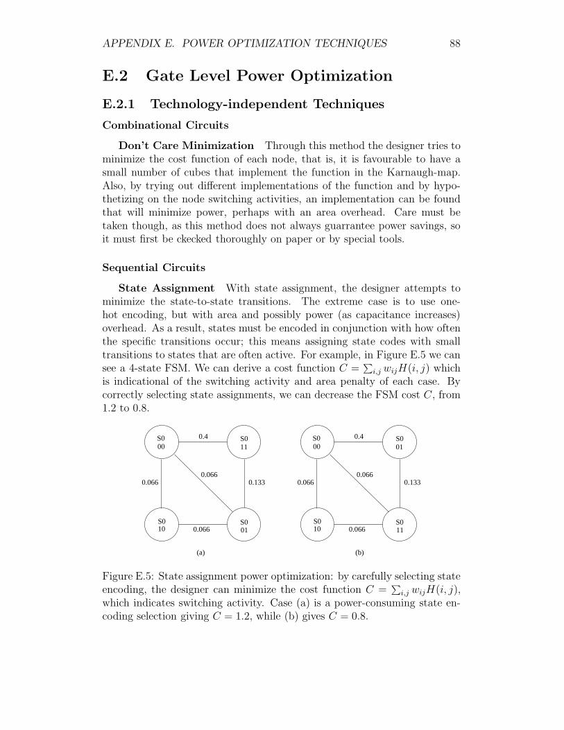
APPENDIX E. POWER OPTIMIZATION TECHNIQUES 88
E.2 Gate Level Power Optimization
E.2.1 Technology-independent Techniques
Combinational Circuits
Don’t Care Minimization Through this method the designer tries tominimize the cost function of each node, that is, it is favourable to have asmall number of cubes that implement the function in the Karnaugh-map.Also, by trying out different implementations of the function and by hypo-thetizing on the node switching activities, an implementation can be foundthat will minimize power, perhaps with an area overhead. Care must betaken though, as this method does not always guarrantee power savings, soit must first be ckecked thoroughly on paper or by special tools.
Sequential Circuits
State Assignment With state assignment, the designer attempts tominimize the state-to-state transitions. The extreme case is to use one-hot encoding, but with area and possibly power (as capacitance increases)overhead. As a result, states must be encoded in conjunction with how oftenthe specific transitions occur; this means assigning state codes with smalltransitions to states that are often active. For example, in Figure E.5 we cansee a 4-state FSM. We can derive a cost function C =
∑
i,j wijH(i, j) whichis indicational of the switching activity and area penalty of each case. Bycorrectly selecting state assignments, we can decrease the FSM cost C, from1.2 to 0.8.
(b)
0.1330.066
S000
10S0
0.066
0.066
11S00.4
01S0
0.1330.066
S000
10S0
0.066
0.066
S00.4
S0
01
11
(a)
Figure E.5: State assignment power optimization: by carefully selecting stateencoding, the designer can minimize the cost function C =
∑
i,j wijH(i, j),which indicates switching activity. Case (a) is a power-consuming state en-coding selection giving C = 1.2, while (b) gives C = 0.8.

APPENDIX E. POWER OPTIMIZATION TECHNIQUES 89
FSM Decomposition With this technique, the FSM is divided intoone ore more sub-FSMs; this is done because not all the sub-FSMs will beactive at any time, hence some power management can be achieved. FSMpartitioning into sub-FSMs is carefully carried out in order to minimize inter-FSM communication. The overhead of this method, an example of which canbe seen in Figure E.6, is the area overhead for the addition of the sub-FSMactivation/inactivation logic.
(b)
S0 S1
S2
S3S4
S5
(a)
M2(S3,S4,S5)
(S0,S1,S2)M1
Figure E.6: FSM decomposition power optimization: in (a) we can see atraditional FSM, which can be partinioned into two sub-FSMs, M1 & M2,(b), only one of which will be active at any time.
Retiming & Guarded Evaluation Retiming is a performance ori-ented method. Latches are added to the glitchy nodes and 5-10% powersavings can be achieved in pipelined circuits. Area overhead is not negligi-ble, though. This optimization is not supported by Synopsys Power Com-piler, thus the designer has to perform it on his own (see Figure E.7). Withguarded evaluation, dynamic power management is carried out, but in theGate-Level: guard logic (latches with enable) are added to block inputs.
E.2.2 Technology-dependent Techniques
Technology Mapping
The idea of technology mapping is to hide high-switching nodes inside thegates. If, for example, the tool synthesizes a function f , at first it performs“decomposition of f”, thus building the “subject graph”, which is the circuitthat implements f , built from primitive elements. Next the tool performs“subject graph covering”, that is, it chooses the appropriate gates from thetechnology library, in order to “hide” some high switching activity inside the

APPENDIX E. POWER OPTIMIZATION TECHNIQUES 90
(b)(a)
Figure E.7: Retiming power optimization: lathes are added (b) to glitchynodes; power reduction is in the range of 5-10%, but area overhead can besignificant.
gate; these gates will be directly built on silicon, so their switching activitywill as low possible. An example of this mapping can be seen in Figure E.8.
H
L L
Figure E.8: Technology mapping power optimization: the covered circuit onthe left is the “subject graph”, which is then “covered” into a three inputNAND gate, shown on the right; thus, the high switching internal node ofthe subject graph is “hidden” inside the gate implementation.
Gate Resizing
All technology libraries contain a number of basic primitives (gates, mul-tiplexors, registers), but for every primitive, multiple editions exist, withdifferent characteristics (size, speed, power consumption), as shown in Fig-ure E.9. The synthesis tool chooses which instance to use depending on thecontraints the designer has imposed. Hence, the tool chooses to use fast,but power consuming primitives in the critical path, and small, slow and lowpower primitives for other, non-critical, paths. Power savings can be up to30%.
Buffer Insertion
Having a fully mapped gate level netlist, with exact timing data, we can addbuffers and thus decrease the capacitance and the transition time of a node.For example, in Figure E.10 we can see how a buffer insertion between adriving NAND gate and two receiver flip flops reduces capacitance (hencepower consumption) and node transition time.

APPENDIX E. POWER OPTIMIZATION TECHNIQUES 91
high powerslowlow power
small size medium sizemedium speedmedium power
largefast
Figure E.9: Technology library primitive characteristics: the library containsdifferent editions of the same primitives, which differ in area, speed and powerconsumption. Hence, the synthesis tool can choose to use a specific primitive,depending on the contraints set by the designer.
−Buffer = 1
Internal Power−NAND = 3−FF1, FF2 = 5Total = 13−Tr. time n1 = 4
clkclk
n1 n1 n2
Internal Power
(a) (b)
−NAND = 2.5
−Tr. time n1, n2 = 2Total = 12.5−FF1, FF2 = 4.5
Figure E.10: Buffer insertion power optimization: case (a) shows a NANDgate driving two flip flops in parallel. By adding a buffer in the node (case(b)), NAND gate and flip flop power consumption decrease. Of course, bufferinsertion should be carefully performed: mistakes may increase total power.
Dual-voltage Gates
Gates with low supply voltage consume small amounts of power, but are slow,too. The synthesis tool might be able to replace gates that do not affect thetiming contraints with others of a lower supply voltage (see Figure E.11).Generally speaking, no more than two different supply voltages should beused in a circuit; this method is also preferrably followed locally in a design,as the special circuits needed at the low voltage outputs (level shifters), havelarge area and consume power 3.
3Special algorithms do exist that minimize the use of level shifters.

APPENDIX E. POWER OPTIMIZATION TECHNIQUES 92
(a)
slowlow power
small size
medium sizemedium speedmedium power
largefasthigh power
HVdd (2.5 V)
−fast−high power
slowlow power
small size
medium sizemedium speedmedium power
largefasthigh power
−low power−slow
L Vdd (1.8 V)
(b)
Figure E.11: Dual-voltage gate power optimization: case (a) is a high voltage(2.5V) technology library of three NAND gates, which are fast and non-poweraware. Case (b) is a low voltage (1.8V) version of the same technology; it isslower, but consumes less power.
Leakage Power Minimization
By synthesizing the design with gates of high threshold voltage VThreshold, wecan achieve a minimum leakage power implementation. Timing constraintsare then met by replacing the gates of the critical path with gates of smallerthreshold voltage. Of course, switching power decreases as threshold voltagedrops, and at the same time leakage power increases; thus, care must betaken.
Appendix F
LFSR Random NumberGenerators
Switch verification is a difficult task, with the most challenging part beingthe generation of realistic input traffic that must resemble, as close possible,real internet traffic. Because of the high link bandwidth (almost 10 Gbit/sec)supported by our 32×32 buffered crossbar switch, emulating internet back-bone traffic was desirable. After traffic analysis data is acquired, traffic mustbe generated and sent to the switch inputs. Although this task is usuallyperformed in software 1, generating traffic that follows specific mathematicaldistributions is quite difficult in hardware. In this section we will presentthe most important internet traffic analysis results, and propose a way toproduce number sequences that follow a specific distribution in hardware,especially in FPGAs. Random number generation is mostly analysed, sinceevery other distribution can be implemented by transformating a randomnumber sequence.
F.1 Traffic Analysis
Traffic analyses were found in [23], while a cumulative distribution of packetsizes, and of bytes by the size of packets carrying them is presented in Fig-ure F.1. The figure is a good example of the difference between per-packetand per-byte analyses. As we can see, there is a predominance of smallpackets, with peaks at the common sizes of 44, 552, 576, and 1500 bytes.The small packets, 40-44 bytes in length, include TCP acknowledgementsegments, TCP control segments such as SYN, FIN, and RST packets, andtelnet packets carrying single characters (keystrokes of a telnet session).Many TCP implementations that do not implement Path MTU Discoveryuse either 512 or 536 bytes as the default Maximum Segment Size (MSS)for nonlocal IP destinations, yielding a 552-byte or 576-byte packet size. A
1Such software traffic generation is briefly presented in [19], whereas a more technicaland detailed presentation can be found in [29].
93

APPENDIX F. LFSR RANDOM NUMBER GENERATORS 94
Figure F.1: IP packet length distribution: Data taken from a www.caida.orgyear 2000 simulation.
Maximum Transmission Unit (MTU) size of 1500 bytes is characteristic ofEthernet-attached hosts. Almost 75% of the packets are smaller than thetypical TCP MSS of 552 bytes. Nearly half of the packets are 40 to 44 bytesin length. Note, however, that in terms of bytes, the picture is much differ-ent. While almost 60% of packets are 44 bytes or less, constituting a totalof 7% of the byte volume, over half of the bytes are carried in packets of size1500 bytes or larger.
F.2 Hardware Random Number Generators
Generally speaking, there are several requirements that a random numbergenerator (RNG) must satisfy, the most important being: (a) uniformity,(b) independence, (c) long period, (d) repeatability, (e) portability, and, ofcourse, (f) efficiency [28]. The latter requirement is the most difficult to meetin hardware and the most important, too, as hardware recourses are critical,both for ASICs and FPGAs.
RNGs can be either “truly random” or “pseudo random”, with the for-mer to excibit true randomness (so the value of the next number is unpre-dictable), and the latter to only appear random. Truly RNGs can only be
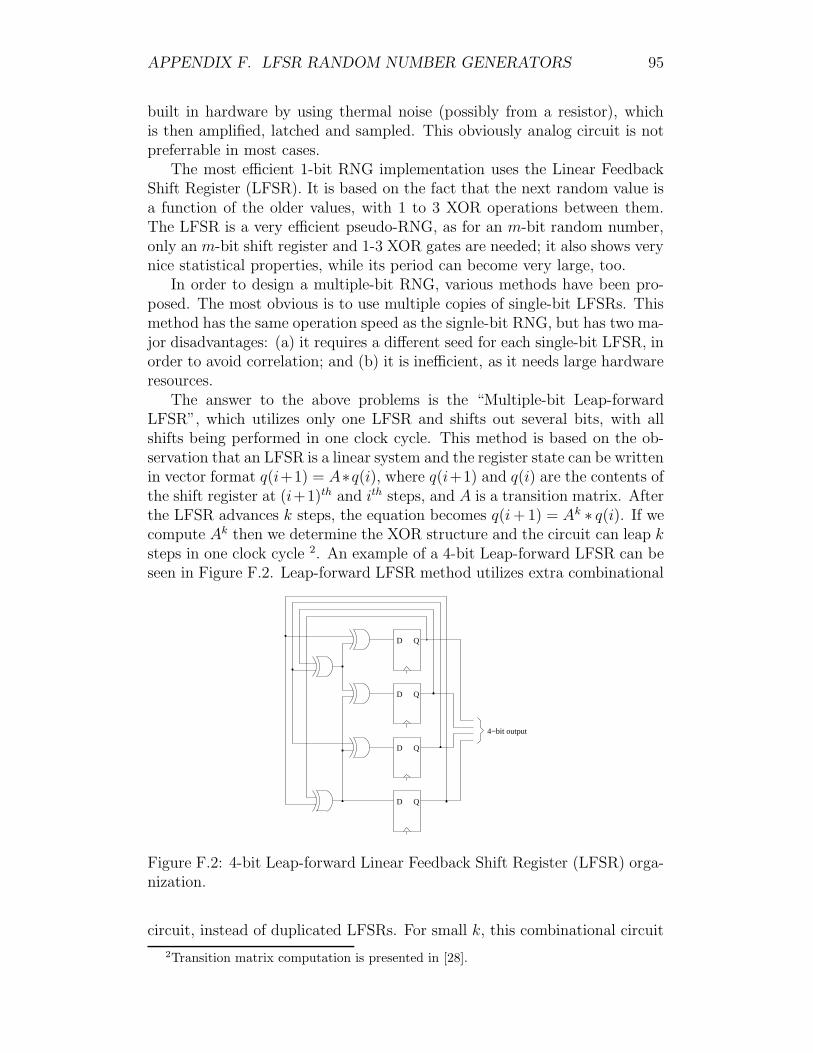
APPENDIX F. LFSR RANDOM NUMBER GENERATORS 95
built in hardware by using thermal noise (possibly from a resistor), whichis then amplified, latched and sampled. This obviously analog circuit is notpreferrable in most cases.
The most efficient 1-bit RNG implementation uses the Linear FeedbackShift Register (LFSR). It is based on the fact that the next random value isa function of the older values, with 1 to 3 XOR operations between them.The LFSR is a very efficient pseudo-RNG, as for an m-bit random number,only an m-bit shift register and 1-3 XOR gates are needed; it also shows verynice statistical properties, while its period can become very large, too.
In order to design a multiple-bit RNG, various methods have been pro-posed. The most obvious is to use multiple copies of single-bit LFSRs. Thismethod has the same operation speed as the signle-bit RNG, but has two ma-jor disadvantages: (a) it requires a different seed for each single-bit LFSR, inorder to avoid correlation; and (b) it is inefficient, as it needs large hardwareresources.
The answer to the above problems is the “Multiple-bit Leap-forwardLFSR”, which utilizes only one LFSR and shifts out several bits, with allshifts being performed in one clock cycle. This method is based on the ob-servation that an LFSR is a linear system and the register state can be writtenin vector format q(i+1) = A∗q(i), where q(i+1) and q(i) are the contents ofthe shift register at (i+1)th and ith steps, and A is a transition matrix. Afterthe LFSR advances k steps, the equation becomes q(i + 1) = Ak
∗ q(i). If wecompute Ak then we determine the XOR structure and the circuit can leap ksteps in one clock cycle 2. An example of a 4-bit Leap-forward LFSR can beseen in Figure F.2. Leap-forward LFSR method utilizes extra combinational
4−bit output
D Q
D Q
D Q
D Q
������
��
������
��
������
� ���
����
������
Figure F.2: 4-bit Leap-forward Linear Feedback Shift Register (LFSR) orga-nization.
circuit, instead of duplicated LFSRs. For small k, this combinational circuit
2Transition matrix computation is presented in [28].

APPENDIX F. LFSR RANDOM NUMBER GENERATORS 96
is not very complex and is thus ideal for FPGAs, since it balances register andcombinational circuitry. However, for large k, the XOR structure grows verylarge and becomes the dominant factor; in that case, a “Lagged Fibonnaci”RNG can be used instead.
F.3 Non-uniform Number Hardware Sequence
Generation
In order to produce general, non-uniform random numbers that follow a spe-cific distribution, a similar procedure can be followed: first we generate auniformly-distributed random number, and then we perform an extra pro-cessing step, in order to produce the desired value. There are two methodsto implement that extra step, but the easiest and most straightforward is the“inverse tranform method”: assuming a random variable X, with a proba-bility distribution function (pdf) P (X = xj) = pj, where j = 1, . . . , m and∑
j pj = 1. We generate an n-bit random number U and set X as
X =
x1 if 0 <= U < p02n
x2 if p02n <= U < p1s
n
· · ·
Hence, in the worst case, we need a 2n by log2m ROM look-up table. Bycomputing the above values off-line, storing them in a ROM and addressingit with a uniformly distributed random number (possibly computed by aLFSR-RNG), the desired values are generated.

Appendix G
Thesis Overview
This thesis was carried out from February 2003 until June 2004 and wascomposed of 5 stages: (a) initial work, (b) switch architecture, HDL codingand verification, (c) synthesis and verification, (d) placement and routing and(e) thesis report. Figure G.1 shows the time spent in each of those stages; itshould be noted that most stages overlapped.
Thesis
Feb 03 Apr 03 Sep 03 Nov 03 May 04 Jun 04
Placement &Initialwork
Sw. architecture, HDL coding &verification
Synthesis &verification routing report
Figure G.1: Project timeline.
Entire code size of the project can be seen in table G.1. “Core VerilogCode” code infers to the 32×32 switch code written from scratch; “Automat-ically Generated Code” had to be produced in order to instantiate the 1024crosspoints and the 32 credit and output schedulers, as well as organize theswitch in columns. This was carried out by a C file. “Miscellaneous VerilogCode” was mostly written for the development of a 4×4 buffered crossbarswitch with WRR schedulers, as well as for tests on LFSR random numbergenerators.
Core Verilog Code 5500Autom. Generated Verilog Code 10500
Miscellaneous Verilog Code 2000Synopsys & SoC Encounter Scripts 800
C Code 600
Table G.1: Thesis code size.
97
Bibliography
[1] “Buffered Crossbar (CICQ) Switch Architecture”, ComputerArchitecture and VLSI Laboratory, Institute of Computer Sci-ence, Foundation for Research and Technology, Hellas (FORTH);http://archvlsi.ics.forth.gr/bufXbar/
[2] Kenji Yoshigoe and Kenneth J. Christensen: “An Evolution to CrossbarSwitches with Virtual Output Queueing and Buffered Cross Points”,IEEE Network, September/October 2003
[3] Yeh, Hluchyj, Acampora: “The Knockout Switch: A Simple, ModularArchitecture for High-Performance Packet Switching”, IEEE Journal ofSelected Areas in Communications, pp. 1274-1283, Oct 1987.
[4] M. Karol, M. Hluchyj, and S. Morgan: “Input versus Output Queueingon a Space Division Packet Switch”, IEEE Trans. Commun., vol. 35,no. 12, Dec. 1987, pp. 1347-56
[5] Altera Corporation: “Crosspoint Switch Matrices in MAXII & MAX 3000A Devices”, Altera Application Note 294 ;http://www.altera.com/literature/an/an294.pdf
[6] Altera Corporation: “Using Stratix GX inSwitch Fabric Systems”, Altera White Paper ;http://www.altera.com/literature/wp/wp switch fabric.pdf
[7] Vinita Singhal, Robert Le: “High-Speed Buffered Crossbar SwitchDesign Using Virtex-EM Devices”, Xilinx Application Note 240 ;http://direct.xilinx.com/bvdocs/appnotes/xapp240.pdf
[8] Xilinx Corporation: “Building Crosspoint Switches with CoolRunner-IICPLDs”, Xilinx Application Note 380 ; http://www.xilinx.com/ publi-cations/products/cool2/apps pdf/xapp380.pdf
[9] Xilinx Corporation; http://www.xilinx.com
[10] Xilinx Corporation: “Rocket IO Multi-Gigabit Tranceiver”;http://www.xilinx.com/products/virtex2pro/rocketio.htm
98

BIBLIOGRAPHY 99
[11] Nick McKeown, Martin Izzard, Adisak Mekkittikul, William Ellersick,Mark Horowitz: “The Tiny Tera: A Packet Switch Core”, HOTI V,Stanford University, August 1996; http://tiny-tera.stanford.edu/tiny-tera/papers/papers/HOTI 96.ps
[12] Nick McKeown: “The iSLIP Scheduling Algorithm for Input-Queued Switches”, IEEE/ACM Transactions on Network-ing, vol. 7, no. 2, April 1999, pp. 188-201; http://tiny-tera.stanford.edu/ nickm/papers/ToN April 99.pdf
[13] T. Anderson et al.: “High-Speed Switch Scheduling for Local-Area Net-works”, ACM Trans. Computer Systems, vol. 11, no. 4, Nov. 1993, pp.319-52
[14] K. Yoshigoe and K. Christensen: ”A Parallel-Polled Virtual OutputQueued Switch with a Buffered Crossbar”, 2001 IEEE Workshop onHigh Performance Switching and Routing, pp. 271-275, May 2001;http://www.csee.usf.edu/ kyoshigo/hpsr01.pdf
[15] K. Yoshigoe, K. Christensen, and A. Jacob: ”The RR/RRCICQ Switch: Hardware Design for 10-Gbps Link Speed”, Pro-ceedings of the IEEE 2003 International Performance, Comput-ing, and Communications Conference, pp. 481-485, April 2003;http://www.csee.usf.edu/ kyoshigo/ipccc03.pdf
[16] Christopher Heer, Andreas Kirstadter, Christian Sauer: “Self-Routing Crossbar Switch with Internal Contention Resolution”, In-ternational IEEE Conference on Electronics, Circuits, and Systems,ICECS 2001, Sept. 2-5, Malta; http://www.lkn.ei.tum.de/lkn/ mitar-beiter/akirstaedter/papers/2001 ICECS Chipset.pdf
[17] Heikki Kariniemi, Jari Nurmi: “A Crossbar-based ATMSwitch on FPGA for 2.488 Gbits/s CATV Network withScalable Header Remapping Function”, Institute of Digitaland Computer Systems, Tampere University of Technology ;http://www.scit.wlv.ac.uk/ in8189/CSNDSP2002/Papers/C1/C1.4.pdf
[18] F. Abel, C. Minkenberg, R. Luijten, M. Gusat, I. Illiadis: “A Four-Terabit Packet Switch Supporting Long Round-Trip Times”, IEEE Mi-cro Magazine, vol. 23, no. 1, Jan/Feb 2003, pp. 10-24
[19] M. Katevenis, G. Passas, D. Simos, I. Papaefstathiou, N.Chrysos: “Variable Packet Size Buffered Crossbar (CICQ)Switches”, Proc. IEEE International Conference on Communica-tions (ICC 2004), Paris, France, June 2004, vol. 2, pp. 1090-1096;http://archvlsi.ics.forth.gr/bufxbar/
[20] Cadence Corporation; http://www.cadence.com

BIBLIOGRAPHY 100
[21] UMC 0.18 micron Libraries; http://www.umc.com/english/design/b3.asp
[22] Xiang Li: “Saving Power with Power Compiler”;http://vlsi1.engr.utk.edu/ xiang/652/POWER-COMPILER.ppt
[23] Cooperative Association for Internet Data Analysis: “Packet LengthDistributions”; http://www.caida.org
[24] N. Chrysos, M. Katevenis: “Mutliple Priorities in a Two-Lane Buffered Crossbar”, to be published in Globecom 2004 ;http://archvlsi.ics.forth.gr/bufxbar/mprio bxb chrys 04-03.pdf
[25] S. Devadas and S. Malik: “A Survey of OptimizationTechniques Targeting Low Power VLSI Circuits”, Proc.IEEE Design Automation Conf., pp. 242-247, June 1995;http://portal.acm.org/ ft gateway.cfm?id=217536&type=pdf&coll=portal&dl=ACM&CFID=24235476&CFTOKEN=52253054
[26] Altera Corporation: “System-on-a-Programmable-Chip DevelopmentBoard User Guide”; http://www.altera.com/literature/ug/sopcug.pdf
[27] Ahmed Younis et al.: “A Low Jitter, Low Power, CMOS 1.25-3.125 Gbps Tranceiver”, Proc. of 2001 ESSCIRC, pp. 148-151;http://www.imec.be/esscirc/esscirc2001/Proceedings/data/79.pdf
[28] Pong P. Chu and Robert E. Jones: “Design Techniquesof FPGA Based Random Number Generator”, Militaryand Aerospace Applications of Programmable Devices andTechnologies Conference, 1999 ; http://academic.csuohio.edu:8080/chup/chu web stuff/research stuff/Random.PDF
[29] Georgios Passas: “Performance Evaluation of VariablePacket Size Buffered Crossbar Switches”, Institute of Com-puter Science, FORTH, Technical Report 328, Heraklion,Crete, Greece, November 2003; ftp://ftp.ics.forth.gr/tech-reports/2003/2003.TR328 Evaluation Packet-Size Buffered Crossbar Switches.pdf
[30] Quantum Flow Control (QFC) Alliance: “Quantum Flow Control: Acell-relay protocol supporting an Available Bit Rate Service”, version2.0, July 1995; originally at http://www.qfc.org but no longer there –copy at http://archvlsi.ics.forth.gr/ kateveni/534/qfc/
[31] “CS-534, Packet Switch Architecture”, Computer Science Department,University of Crete, lecture notes; http://www.archvlsi.ics.forth.gr/ kat-eveni/534/04a/s22 chip.html
[32] William J. Dally, John Poulton: “Digital Systems Engineering”, Cam-bridge University Press, ISBN 0521592925
BIBLIOGRAPHY 101
[33] Network Equipment Building Standards (NEBS); http://www.nebs-faq.com/, http://www.telcordia.com/
[34] K. Harteros: “Fast Parallel Comparison Circuits for Schedul-ing”, Institute of Computer Science, FORTH, Techni-cal Report FORTH-ICS/TR-304, 78 pages, March 2002;http://archvlsi.ics.forth.gr/muqpro/cmpTree.html
[35] Cyriel Minkenberg, Ronald P. Luijten, Francois Abel, Wolf-gang Denzel, Mitchell Gusat: “Current Issues in PacketSwitch Design”, HOTNETS ‘02, 10/02 Princeton, NJ, USA;http://www.acm.org/sigs/sigcomm/HotNets-I/papers/minkenberg.pdf
[36] “International Technology Roadmap for Semi-conductors”, 2003 Edition, Executive Summary;http://public.itrs.net/Files/2003ITRS/Home2003.htm
[37] “ECE260B - CSE241A”, University of California, San Diego, Winter2004, lecture notes; http://vlsicad.ucsd.edu/courses/ece260b-w04/
[38] “ECE260B - CSE241A: Packaging”, University of California, San Diego,Winter 2004, lecture notes; http://vlsicad.ucsd.edu/courses/ece260b-w04/ece260b-w04-packaging.pdf
[39] IBM Microelectronics Presentation: “Embedded DRAMComparison Charts”, IBM Microelectronics; http://www-306.ibm.com/chips/techlib/techlib.nsf/products/Embedded DRAM
[40] John Barth, Darren Anand, Jeff Dreibelbis, Erik Nelson: “A300MHz Multi-Banked eDRAM Macro Featuring GND Sense,Bit-Line Twisting and Direct Reference Cell Write”, ISSCC2002, Session 9, DRAM and Ferroelectric Memories, 9.3;http://www-306.ibm.com/chips/techlib/ techlib.nsf/techdocs/48D7E84C4F67E55287256DD700021AA1/$file/isscc02 D09 3.pdf
[41] Chorng-Lii Hwang et al.: “A 2.9ns Random Access Cycle Em-bedded DRAM with a Destructive-Read Architecture”, IBM Micro-electronics; http://www-306.ibm.com/ chips/techlib/techlib.nsf/ tech-docs/E95CC111124D5A5587256DD6007DE26D
[42] Steve Tomashot: “An Embedded DRAM Approach”, IBM Cor-poration; http://www-306.ibm.com/ chips/techlib/techlib.nsf/ tech-docs/C4DA54943C004A1987256DC8004EA766/$file/emdramprez.pdf
[43] “eSi-RAM/2PTM Two-Port Register File SRAM”, 512 Words 32 Bitsper word, Data Sheet

BIBLIOGRAPHY 102
[44] Terry Tao Ye, Luca Benini, Giovanni De Micheli: “Analysis of PowerConsumption on Switch Fabrics in Network Routers”, Proceedings ofDesign Automation Conference, DAC 2002, IEEE, pp. 524 -529, June,2002; http://www.gigascale.org/pubs/408/34-02-ye.pdf
[45] Hang-Sheng Wang, Li-Shiuan Peh, Sharad Malik: “A PowerModel for Routers: Modelling the Alpha 21364 and In-finiband Routers”, IEEE Micro, Jan-Feb 2003, pp. 26-35;http://www.princeton.edu/ peh/publications/powermodel.pdf
[46] Synopsys Corporation; http://www.synopsys.com
[47] “Power Compiler User Guide”, Synopsys Corporation, June 2003