design guide for rf low-noise transistor in lidar applications
TRANSCRIPT
Application Note Please read the Important Notice and Warnings at the end of this document V X.Y
www.infineon.com page 1 of 14 2018-05-23
AN_1809_PL32_1811_161136
Design guide for RF low-noise transistor in LiDAR
applications
RF bipolar transistor
About this document
Scope and purpose
This application note provides an application circuit design example of broadband low-noise signal amplification with Infineon’s low-noise silicon germanium carbon (SiGe:C) transistor BFR740L3RH for light detection and ranging (LiDAR). In this document the transistor circuit schematic, PCB layout and measurement
results are shown.
Intended audience
This document is intended for engineers who need to design LiDAR application circuits.
Table of contents
About this document ............................................................................................................................................. 1
Table of contents ................................................................................................................................................... 1
1 Introduction ................................................................................................................................................. 2 1.1 LiDAR architecture ................................................................................................................................... 2 1.2 Infineon RF transistors family ................................................................................................................. 3
2 LiDAR LNA circuit with the BFR740L3RH transistor ...................................................................................... 4
2.1 Performance overview ............................................................................................................................ 4
2.2 Schematic ................................................................................................................................................ 4 2.3 Bill of materials (BOM) ............................................................................................................................ 5
2.4 Evaluation board and layout information .............................................................................................. 6
2.5 Measurement results of the LiDAR LNA with BFR740L3RH transistor ................................................... 7
3 Authors ...................................................................................................................................................... 12
Revision history ................................................................................................................................................... 13
Application Note 2 of 14 V X.Y
2018-05-23
Design guide for RF low-noise transistor in LiDAR applications RF bipolar transistor
Introduction
1 Introduction
1.1 LiDAR architecture
LiDAR is a remote sensing technique that measures the distance to a target and creates a 3D map of the target
object. Its versatility and high resolution make it suitable for application in guidance, rangefinders, drones, laser safety scanners, architectural surveying equipment, gas analysis, retinal imaging, robotics, etc.
LiDAR uses different architectures as direct and indirect time-of-flight (ToF) measurement, or triangulation for
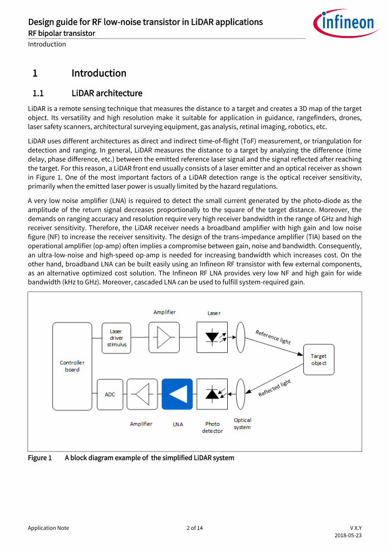
detection and ranging. In general, LiDAR measures the distance to a target by analyzing the difference (time delay, phase difference, etc.) between the emitted reference laser signal and the signal reflected after reaching the target. For this reason, a LiDAR front end usually consists of a laser emitter and an optical receiver as shown
in Figure 1. One of the most important factors of a LiDAR detection range is the optical receiver sensitivity, primarily when the emitted laser power is usually limited by the hazard regulations.
A very low noise amplifier (LNA) is required to detect the small current generated by the photo-diode as the
amplitude of the return signal decreases proportionally to the square of the target distance. Moreover, the
demands on ranging accuracy and resolution require very high receiver bandwidth in the range of GHz and high receiver sensitivity. Therefore, the LiDAR receiver needs a broadband amplifier with high gain and low noise
figure (NF) to increase the receiver sensitivity. The design of the trans-impedance amplifier (TIA) based on the operational amplifier (op-amp) often implies a compromise between gain, noise and bandwidth. Consequently,
an ultra-low-noise and high-speed op-amp is needed for increasing bandwidth which increases cost. On the
other hand, broadband LNA can be built easily using an Infineon RF transistor with few external components, as an alternative optimized cost solution. The Infineon RF LNA provides very low NF and high gain for wide bandwidth (kHz to GHz). Moreover, cascaded LNA can be used to fulfill system-required gain.
Figure 1 A block diagram example of the simplified LiDAR system
Application Note 3 of 14 V X.Y
2018-05-23
Design guide for RF low-noise transistor in LiDAR applications RF bipolar transistor
Introduction
1.2 Infineon RF transistors family
Infineon Technologies provides high-performance RF transistors suitable for LiDAR LNA applications. Infineon’s
reliable high-volume RF transistor offers exceptionally low NF, high gain and high linearity at low power
consumption levels for RF applications. The seventh-generation transistor is based on robust ultra-low-noise SiGe:C technologies. Their optimized inner transistor cell structure leads to best-in-class power gains and NFs
in a broad bandwidth, including LiDAR operating frequency. The transistor optimizes design flexibility to suit customer requirements.
Application Note 4 of 14 V X.Y
2018-05-23
Design guide for RF low-noise transistor in LiDAR applications RF bipolar transistor
LiDAR LNA circuit with the BFR740L3RH transistor
2 LiDAR LNA circuit with the BFR740L3RH transistor
2.1 Performance overview
The following table shows the LiDAR LNA performance with RF low-noise bipolar transistor BFR740L3RH.
Table 1 Summary of measurement results for the LiDAR LNA with BFR740L3RH transistor
Parameter Symbol Value Unit Notes
Device
BFR740L3RH
Bias voltage VCC 3.3 V
Bias current ICC 13 mA
3 dB bandwidth f3 dB 2.8 kHz - 450 MHz
Frequency f 10 200 400 MHz
Gain G 22.2 21.8 20.6 dB
NF NF 1.0 1.0 1.0 dB
Input return loss RLin 17.2 16 17.9 dB
Output return loss RLout 22.1 16.1 12.7 dB
Reverse isolation ISOrev 26.9 27.1 27.5 dB
Output 1 dB compression point OP1dB 0.4 0.0 0.2 dBm
Output third order interception point
OIP3 9.2 7.3 5.6 dBm Power at input: -35 dBm, Tone spacing: 1 MHz
Stability K >1
Measured from 300 kHz to 10 GHz
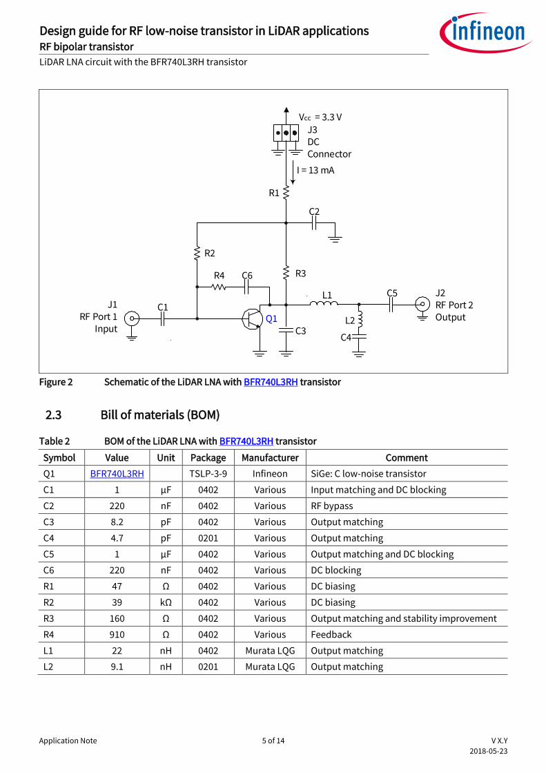
2.2 Schematic
The following figure shows the general schematic of the LiDAR LNA with BFR740L3RH RF low-noise transistor. In
the LNA circuit, resistors R1, R2 and R3 stand for transistor voltage and current bias; meanwhile, R1 and R3 form
a negative DC feedback mechanism to stabilize the transistor bias points in various conditions. Resistor R4 and capacitor C6 serve as the negative feedback to improve input and output impedance matching and in
conjunction with the resistor R3 achieve flat gain over the operating frequency. The transistor’s input matching is performed by the capacitors C1, C6 and the resistor R4. The network of R3, C3, C4, C5, L1 and L2 matches the
transistor to the output port. Capacitor C2 works as an RF bypass which also suppresses low-frequency noise. In general, resistors R3 and R4 stabilize the circuit, whose stability is measured up to 10 GHz.
Application Note 5 of 14 V X.Y
2018-05-23
Design guide for RF low-noise transistor in LiDAR applications RF bipolar transistor
LiDAR LNA circuit with the BFR740L3RH transistor
Q1
J3DC Connector
C1
Vcc = 3.3 V
C5
C2
R3
J2RF Port 2Output
J1RF Port 1
Input
C6R4
I = 13 mA
R2
R1
L2
C4C3
L1
Figure 2 Schematic of the LiDAR LNA with BFR740L3RH transistor
2.3 Bill of materials (BOM)
Table 2 BOM of the LiDAR LNA with BFR740L3RH transistor
Symbol Value Unit Package Manufacturer Comment
Q1 BFR740L3RH
TSLP-3-9 Infineon SiGe: C low-noise transistor
C1 1 μF 0402 Various Input matching and DC blocking
C2 220 nF 0402 Various RF bypass
C3 8.2 pF 0402 Various Output matching
C4 4.7 pF 0201 Various Output matching
C5 1 μF 0402 Various Output matching and DC blocking
C6 220 nF 0402 Various DC blocking
R1 47 Ω 0402 Various DC biasing
R2 39 kΩ 0402 Various DC biasing
R3 160 Ω 0402 Various Output matching and stability improvement
R4 910 Ω 0402 Various Feedback
L1 22 nH 0402 Murata LQG Output matching
L2 9.1 nH 0201 Murata LQG Output matching
Application Note 6 of 14 V X.Y
2018-05-23
Design guide for RF low-noise transistor in LiDAR applications RF bipolar transistor
LiDAR LNA circuit with the BFR740L3RH transistor
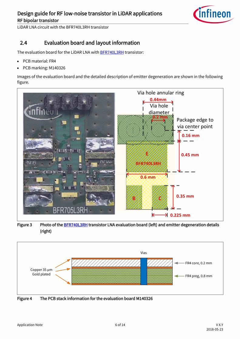
2.4 Evaluation board and layout information
The evaluation board for the LiDAR LNA with BFR740L3RH transistor:
PCB material: FR4
PCB marking: M140326
Images of the evaluation board and the detailed description of emitter degeneration are shown in the following figure.
BFR740L3RH
Package edge to via center point
Via hole annular ring
0.16 mm
E
B C
0.2 mm
Via hole diameter
0.44mm
0.35 mm
0.225 mm
0.45 mm
0.6 mm
Figure 3 Photo of the BFR740L3RH transistor LNA evaluation board (left) and emitter degeneration details
(right)
Copper 35 µmGold plated
FR4 core, 0.2 mm
FR4 preg, 0.8 mm
Vias
Figure 4 The PCB stack information for the evaluation board M140326
Application Note 7 of 14 V X.Y
2018-05-23
Design guide for RF low-noise transistor in LiDAR applications RF bipolar transistor
LiDAR LNA circuit with the BFR740L3RH transistor
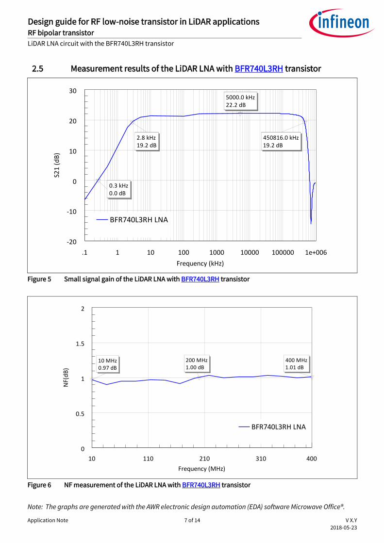
2.5 Measurement results of the LiDAR LNA with BFR740L3RH transistor
Figure 5 Small signal gain of the LiDAR LNA with BFR740L3RH transistor
Figure 6 NF measurement of the LiDAR LNA with BFR740L3RH transistor
Note: The graphs are generated with the AWR electronic design automation (EDA) software Microwave Office®.
.1 1 10 100 1000 10000 100000 1e+006
Frequency (kHz)
-20
-10
0
10
20
30
S21
(d
B)
0.3 kHz0.0 dB
2.8 kHz19.2 dB
450816.0 kHz19.2 dB
5000.0 kHz22.2 dB
BFR740L3RH LNA
10 110 210 310 400
Frequency (MHz)
0
0.5
1
1.5
2
NF(
dB
)
10 MHz0.97 dB
400 MHz1.01 dB
200 MHz1.00 dB
BFR740L3RH LNA
Application Note 8 of 14 V X.Y
2018-05-23
Design guide for RF low-noise transistor in LiDAR applications RF bipolar transistor
LiDAR LNA circuit with the BFR740L3RH transistor
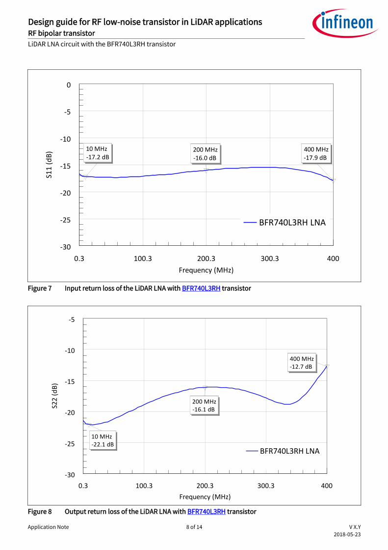
Figure 7 Input return loss of the LiDAR LNA with BFR740L3RH transistor
Figure 8 Output return loss of the LiDAR LNA with BFR740L3RH transistor
0.3 100.3 200.3 300.3 400
Frequency (MHz)
-30
-25
-20
-15
-10
-5
0
S11
(d
B) 400 MHz
-17.9 dB200 MHz-16.0 dB
10 MHz-17.2 dB
BFR740L3RH LNA
0.3 100.3 200.3 300.3 400
Frequency (MHz)
-30
-25
-20
-15
-10
-5
S22
(d
B)
400 MHz-12.7 dB
200 MHz-16.1 dB
10 MHz-22.1 dB
BFR740L3RH LNA
Application Note 9 of 14 V X.Y
2018-05-23
Design guide for RF low-noise transistor in LiDAR applications RF bipolar transistor
LiDAR LNA circuit with the BFR740L3RH transistor
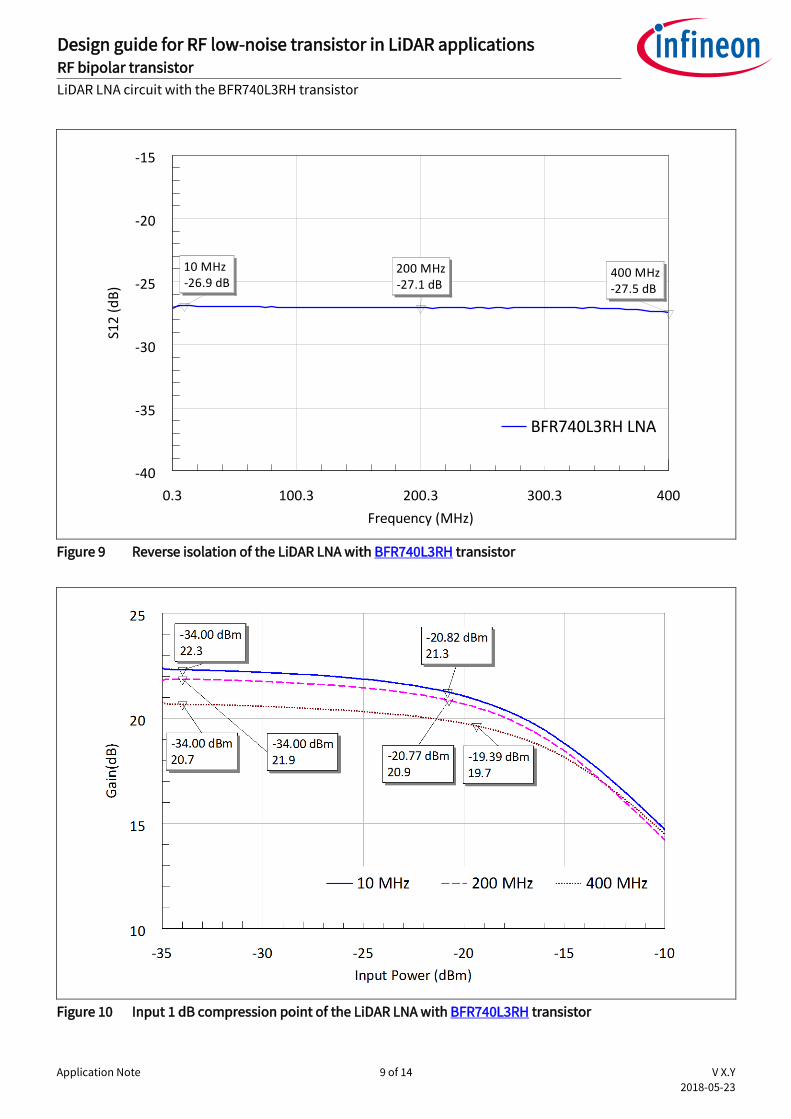
Figure 9 Reverse isolation of the LiDAR LNA with BFR740L3RH transistor
Figure 10 Input 1 dB compression point of the LiDAR LNA with BFR740L3RH transistor
0.3 100.3 200.3 300.3 400
Frequency (MHz)
-40
-35
-30
-25
-20
-15
S12
(d
B)
400 MHz-27.5 dB
200 MHz-27.1 dB
10 MHz-26.9 dB
BFR740L3RH LNA
Application Note 10 of 14 V X.Y
2018-05-23
Design guide for RF low-noise transistor in LiDAR applications RF bipolar transistor
LiDAR LNA circuit with the BFR740L3RH transistor
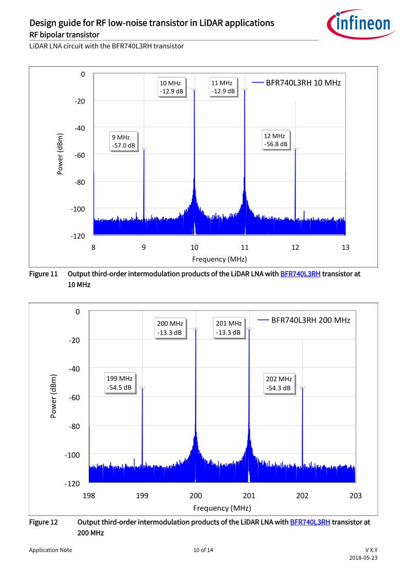
Figure 11 Output third-order intermodulation products of the LiDAR LNA with BFR740L3RH transistor at
10 MHz
Figure 12 Output third-order intermodulation products of the LiDAR LNA with BFR740L3RH transistor at
200 MHz
8 9 10 11 12 13
Frequency (MHz)
-120
-100
-80
-60
-40
-20
0
Po
wer
(d
Bm
)
11 MHz-12.9 dB
10 MHz-12.9 dB
9 MHz-57.0 dB
12 MHz-56.8 dB
BFR740L3RH 10 MHz
198 199 200 201 202 203
Frequency (MHz)
-120
-100
-80
-60
-40
-20
0
Po
wer
(d
Bm
)
202 MHz
-54.3 dB
201 MHz
-13.3 dB
199 MHz
-54.5 dB
200 MHz
-13.3 dB
BFR740L3RH 200 MHz
Application Note 11 of 14 V X.Y
2018-05-23
Design guide for RF low-noise transistor in LiDAR applications RF bipolar transistor
LiDAR LNA circuit with the BFR740L3RH transistor
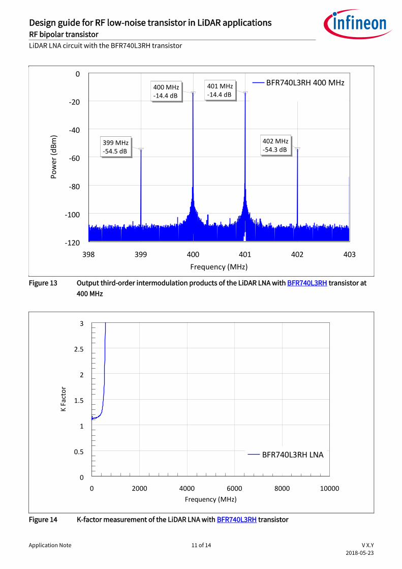
Figure 13 Output third-order intermodulation products of the LiDAR LNA with BFR740L3RH transistor at
400 MHz
Figure 14 K-factor measurement of the LiDAR LNA with BFR740L3RH transistor
398 399 400 401 402 403
Frequency (MHz)
-120
-100
-80
-60
-40
-20
0
Po
wer
(d
Bm
)
402 MHz-54.3 dB
399 MHz-54.5 dB
401 MHz-14.4 dB
400 MHz-14.4 dB
BFR740L3RH 400 MHz
0 2000 4000 6000 8000 10000
Frequency (MHz)
0
0.5
1
1.5
2
2.5
3
K F
acto
r
BFR740L3RH LNA
Application Note 12 of 14 V X.Y
2018-05-23
Design guide for RF low-noise transistor in LiDAR applications RF bipolar transistor
Authors
3 Authors
Mamun Md Abdullah Al, RF application engineer of business unit RF and sensors.
Dr. Jie Fang, RF staff application engineer of business unit RF and sensors.
Application Note 13 of 14 V X.Y
2018-05-23
Design guide for RF low-noise transistor in LiDAR applications RF bipolar transistor
Revision history
Revision history
Document version
Date of release Description of changes

Trademarks All referenced product or service names and trademarks are the property of their respective owners.
Edition 2018-05-23
AN_1809_PL32_1811_161136
Published by
Infineon Technologies AG
81726 Munich, Germany
© 2018 Infineon Technologies AG.
All Rights Reserved.
Do you have a question about this document?
Email: [email protected]
Document reference
IMPORTANT NOTICE The information contained in this application note is given as a hint for the implementation of the product only and shall in no event be regarded as a description or warranty of a certain functionality, condition or quality of the product. Before implementation of the product, the recipient of this application note must verify any function and other technical information given herein in the real application. Infineon Technologies hereby disclaims any and all warranties and liabilities of any kind (including without limitation warranties of non-infringement of intellectual property rights of any third party) with respect to any and all information given in this application note. The data contained in this document is exclusively intended for technically trained staff. It is the responsibility of customer’s technical departments to evaluate the suitability of the product for the intended application and the completeness of the product information given in this document with respect to such application.
For further information on the product, technology, delivery terms and conditions and prices please contact your nearest Infineon Technologies office (www.infineon.com).
WARNINGS Due to technical requirements products may contain dangerous substances. For information on the types in question please contact your nearest Infineon Technologies office. Except as otherwise explicitly approved by Infineon Technologies in a written document signed by authorized representatives of Infineon Technologies, Infineon Technologies’ products may not be used in any applications where a failure of the product or any consequences of the use thereof can reasonably be expected to result in personal injury.