design, fabrication, and characterization of all-inorganic
TRANSCRIPT

University of Arkansas, FayettevilleScholarWorks@UARK
Theses and Dissertations
5-2018
Design, Fabrication, and Characterization of All-Inorganic Quantum Dot Light Emitting DiodesRamesh VasanUniversity of Arkansas, Fayetteville
Follow this and additional works at: http://scholarworks.uark.edu/etd
Part of the Electronic Devices and Semiconductor Manufacturing Commons, Nanoscience andNanotechnology Commons, and the Semiconductor and Optical Materials Commons
This Dissertation is brought to you for free and open access by ScholarWorks@UARK. It has been accepted for inclusion in Theses and Dissertations byan authorized administrator of ScholarWorks@UARK. For more information, please contact [email protected], [email protected].
Recommended CitationVasan, Ramesh, "Design, Fabrication, and Characterization of All-Inorganic Quantum Dot Light Emitting Diodes" (2018). Theses andDissertations. 2737.http://scholarworks.uark.edu/etd/2737

Design, Fabrication, and Characterization of All-Inorganic Quantum Dot Light Emitting Diodes
A dissertation submitted in partial fulfillment
of the requirements for the degree of
Doctor of Philosophy in Engineering
by
Ramesh Vasan
Anna University, India
Bachelor of Engineering in Electronics and Instrumentation, 2010
University of Arkansas
Master of Science in Electrical Engineering, 2013
May 2018
University of Arkansas
This dissertation is approved for recommendation to the Graduate Council
____________________________
Omar Manasreh, Ph.D.
Dissertation Director
_____________________________ ____________________________
Simon Ang, Ph.D. Jingxian Wu, Ph.D.
Committee Member Committee Member
_____________________________
Surendra Singh, Ph.D.
Committee Member
ABSTRACT
Quantum dot light emitting diodes are investigated as a replacement to the existing
organic light emitting diodes that are commonly used for thin film lighting and display
applications. In this, all-inorganic quantum dot light emitting diodes with inorganic quantum dot
emissive layer and inorganic charge transport layers are designed, fabricated, and characterized.
Inorganic materials are more environmentally stable and can handle higher current densities than
organic materials. The device consists of CdSe/ZnS alloyed core/shell quantum dots as the
emissive layer and metal oxide charge transport layer. The charge transport in these devices is
found to occur through resonant energy transfer and direct charge injection.
Nickel oxide thin film is engineered with defect states within the bandgap by changing
the stoichiometry of film. These defect states take part in the charge transport via resonant
energy transfer mechanism. The energy transfer mechanism is modeled by measuring the
lifetime of quantum dots in the presence of nickel oxide thin film. Energy transfer between
nickel oxide defect states and quantum dots occurs at time scales as low as 0.26 ns. This
mechanism is exploited to fabricate high efficiency light emitting diodes. Efficient green,
yellow, and red emitting devices are fabricated and characterized. The peak external quantum
efficiencies of 11.4%, 1.6% and 6.04% are obtained for green, yellow, and red emitting devices,
respectively. The performance of green LED is much better than that of the other two colors as
the photoluminescence quantum yield of green quantum dots are much higher than the other two
quantum dot samples.
Nickel oxide is also synthesized as nanoparticles for potential application in hole
transport. Charge transport in devices with nickel oxide nanoparticles occurs via direct charge
injection mechanism. The nanoparticles are near-stoichiometric with very low defect densities.
The quantum dots exhibit shorter average lifetimes when mixed with nickel oxide nanoparticle
powder indicating a favorable band alignment for direct charge injection. Quantum dot LED is
fabricated with nickel oxide nanoparticle hole transport layer and red emitting quantum dots.
The light output characteristics are evaluated and a peak external quantum efficiency of 2.36% is
obtained.

@2018 by Ramesh Vasan
All Rights Reserved

ACKNOWLEDGEMENTS
First of all, I would like to thank my family for their love and support. Without their
support it would not have been possible for me to complete my graduate study.
I would like to express my deep gratitude to my graduate advisor and dissertation
director, Dr. Omar Manasreh for providing me an opportunity to do this research project. His
guidance and support for the past seven years has been invaluable in completing my studies.
I am thankful to Dr. Simon Ang, Dr. Jingxian Wu, and Dr. Surendra Singh for being in
my dissertation committee and providing their valuable expertise in completing this work.
I would like to thank Dr. Colin Heyes, his group members, and post-doctoral researcher
Dr. Feng Gao from the Chemistry department for helping me understand the charge transport in
quantum dot LED investigated in this project.
I am thankful to Dr. Mourad Benamara, Dr. Andrian Kuchuk, and Mr. Timothy Morgan
from the Institute of Nanoscience and engineering for helping me with several material
characterization measurements.
I wish to thank Mr. Haider Salman, Mr. Mohammad Marie and other past and present
group members for their support and help in completing this project.
This work was supported by the NASA-EPSCoR program (Grant 242026-
1BBX11AQ36A).
TABLE OF CONTENTS
1. Introduction…………………………………………………………………………………..1
1.1. Solid State Lighting………………………………………………………………………2
1.1.1. LED parameters………………………………………………………………….10
1.2. Thin film LED technologies…………………………………………………………….11
1.2.1. Organic LED……………………………………………………………………..11
1.2.2. Quantum dot LED………………………………………………………………..14
1.3. Research Objectives……………………………………………………………………..19
2. Experimental Procedures…………………………………………………………………..21
2.1. Material Synthesis, sample and device fabrication……………………………………...21
2.1.1. CdSe/ZnS core shell alloyed quantum dots……………………………………...21
2.1.2. Nickel oxide synthesis…………………………………………………………...24
2.1.2.1. Thin film…………………………………………………………………24
2.1.2.2. Nanoparticles…………………………………………………………….26
2.1.3. Zinc oxide nanoparticles…………………………………………………………26
2.1.4. Quantum dots/nickel oxide thin film bilayer sample…………………………….27
2.1.5. Nickel oxide Schottky diode……………………………………………………..28
2.1.6. Thin film transistor………………………………………………………………29
2.1.7. QLED devices fabrication………………………………………………………..30
2.2. Characterization tools…………………………………………………………………...31
2.2.1. UV-Vis spectroscopy…………………………………………………………….31
2.2.2. Luminescence……………………………………………………………………32
2.2.3. Time resolved photoluminescence……………………………………………….34

2.2.4. Current-Voltage Characteristics………………………………………………….35
2.2.5. Raman spectroscopy……………………………………………………………..37
2.2.6. X-ray Diffraction………………………………………………………………...39
2.2.7. X-ray Photoelectron Spectroscopy………………………………………………40
2.2.8. Atomic Force Microscope………………………………………………………..42
3. Results and Discussions…………………………………………………………………….44
3.1. Material Characterization……………………………………………………………….44
3.1.1. CdSe/ZnS alloyed core/shell quantum dots……………………………………...44
3.1.1.1. Optical Properties………………………………………………………...44
3.1.1.2. Lifetime measurements…………………………………………………..47
3.1.2. Nickel oxide thin film……………………………………………………………50
3.1.2.1. Structural properties……………………………………………………...50
3.1.2.2. Morphological properties………………………………………………...58
3.1.2.3. Optical properties………………………………………………………...59
3.1.2.4. Electrical Properties……………………………………………………...61
3.1.3. Nickel oxide nanoparticles……………………………………………….………67
3.1.3.1. Structural and compositional properties…………………………………67
3.1.3.2. Optical properties………………………………………………………...70
3.1.4. Zinc oxide nanoparticles…………………………………………………………71
3.1.4.1. Structural properties……………………………………………………...71
3.1.4.2. Optical properties………………………………………………………...72
3.1.4.3. Electrical properties…………………………………...…………………73
3.2. Charge transport model…………………………………….……………………………74

3.2.1. Resonant energy transfer ……………...…………………………………………74
3.2.2. Direct charge injection ………………..…………………………………………83
3.3. QLED device results…………………………………………………………………….85
3.3.1. All-inorganic QLED with nickel oxide thin film HTL………..…………………85
3.3.1.1. Green emitting QLED……………………………………………………85
3.3.1.2. Yellow emitting QLED…………………………………..………………90
3.3.1.3. Red emitting QLED………...……………………………………………94
3.3.2. Hybrid QLED with PEDOT:PSS/nickel oxide nanoparticles HTL……….……100
3.3.2.1. Red emitting hybrid QLED…………………………………………..…100
4. Conclusion and Future work…………………………………………………………..…104
4.1. Conclusion…………………………………………………………………..…………104
4.2. Future work………………………………………………………………………….…105
References………………………………………………………………………………….106

LIST OF FIGURES
Figure 1.1. Schematic of a solid state LED chip that is packaged inside a plastic casing………..3
Figure 1.2. The band diagram schematics of (a) p-type, (b) n-type and (c) p-n junction are shown
with the EF…………………………………………………………………………………………6
Figure 1.3. The band bending of the p-n junction energy band under forward bias voltage is
depicted with quasi fermi levels. The process of charge injection across the junction and
recombination are shown………………………………………………………………………….7
Figure 1.4. (a) White light is generated using blue/UV LED and RGB phosphors or combining
the emission discrete red, green, and blue LEDs in the same package. (b) Cutaway schematic of
phosphor based white LED with yellow phosphor and blue LED……………………………….10
Figure 1.5. The white light quality of LEDs is compared to sunlight, incandescent and compact
fluorescent lamps. [17]…………………………………………………………………………...10
Figure 1.6. The schematic of OLED device that is fabricated on glass substrate by layer-by-layer
deposition. ………………………………………………………………………………………12
Figure 1.7. Progress in white light technologies with prediction that white OLED reaching a
maximum luminous efficacy of 150 lm/W by 2020 [25]………………………………………..13
Figure 1.8. Schematic of (a) organic (b) hybrid and (c) all-inorganic QLED showing the
transport layer and emissive layer is shown……………………………………………………..15
Figure 1.9. Charge transport in QLED is explained using a schematic. The red arrows depict
direct charge injection and green arrows depict the energy transfer mechanism………………..16
Figure 1.10. Progress in the performance of QLED architectures over a period of 30 years that
are commonly reported in literature……………………………………………………………...19
Figure 2.1. Schematics of a (a) conventional core/shell quantum dot and (b) alloyed core/shell
quantum dot are depicting the core/shell interface. (c) The core/shell quantum dots are
synthesized using a Schlenk line and three neck flask setup.……………………………………22
Figure 2.2. (a) The dark green and clear nickel hydroxide sol-gel is used as the precursor to the
formation of nickel oxide thin film. (b) Transparency of nickel oxide thin film on glass is
compared to that of a pristine glass slide………………………………………………………...25
Figure 2.3. Nickel oxide nanoparticles are dispersed in butanol for spin caoting application….26
Figure 2.4. Zinc oxide nanoparticles are dispersed in 1-butanol for spin coating application….27
Figure 2.5. Quantum dots are spin coated on (a) pristine glass slide and (b) nickel oxide to
measure the fluorescence lifetime………………………………………………………………..28
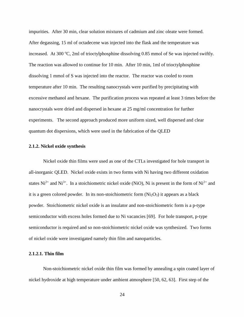
Figure 2.6. A Schottky diode using nickel oxide is fabricated to extract the electrical properties
of the nickel oxide………………………………………………………………………………..29
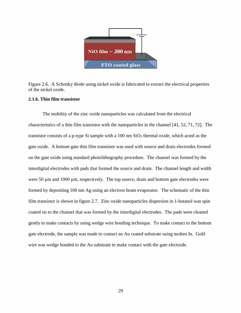
Figure 2.7. A thin film transistor with a bottom gate architecture and zinc oxide nanoparticle
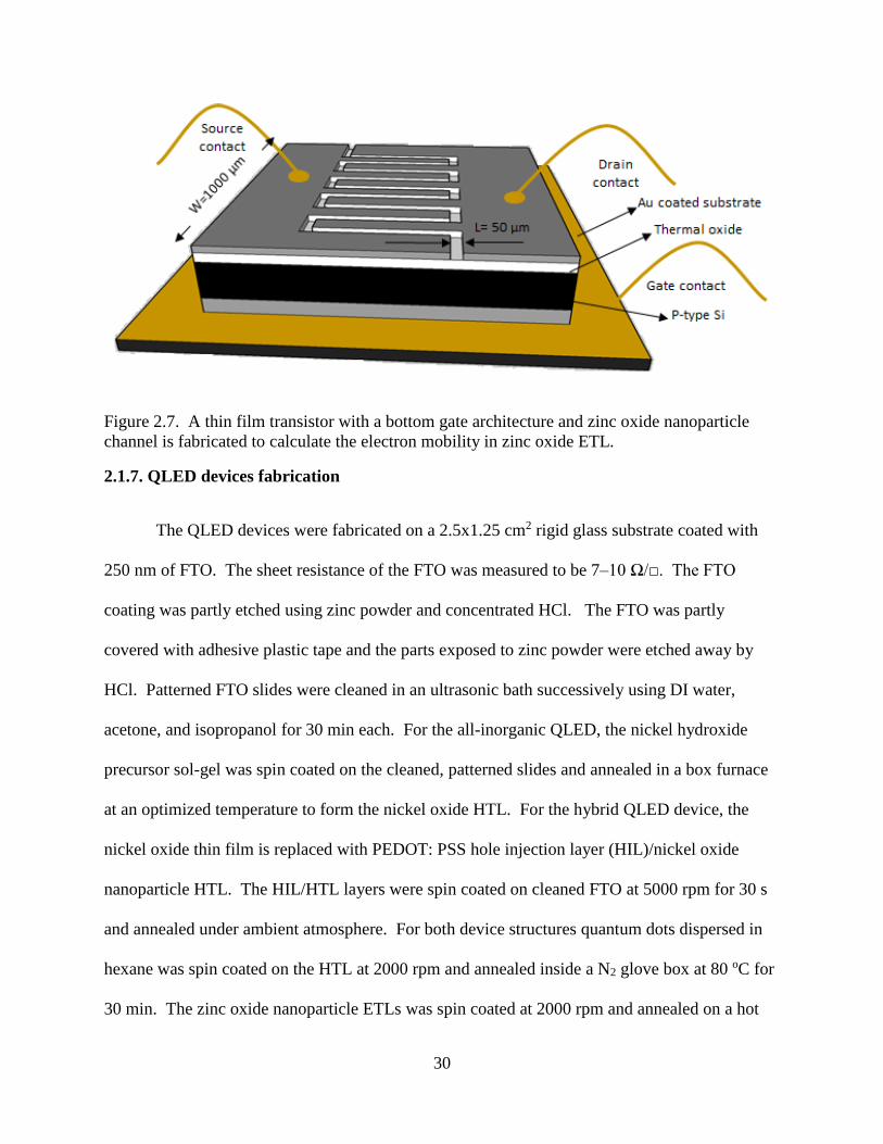
channel is fabricated to calculate the electron mobility in zinc oxide ETL……………………...30
Figure 2.8. Schematics of (a) all-inorganic and (b) hybrid QLEDs that are fabricated using a
layer-by-layer deposition technique……………………………………………………………...31
Figure 2.9. Screenshots of the Keithley test modules used for (a) 2 wire and (b) 3 wire device
measurements…………………………………………………………………………………….37
Figure 2.10. Energy band schematics of Rayleigh and Raman scattering mechanisms. Raman
scattering can be of two types namely Stokes and anti-Stokes shifts……………………………38
Figure 2.11. Auger and photoemission are the processes associated with X-ray photoelectron
spectroscopy……………………………………………………………………………………...40
Figure 2.12. The principle of X-ray photoelectron spectroscopy is shown in the schematic…...41
Figure 2.13. Schematic of an atomic force microscopy used to measure the morphology of the
sample surface is shown………………………………………………………………………….43
Figure 3.1. Optical properties of alloyed quantum dots synthesized by changing the ligand
concentration are evaluated using (a) photoluminescence and (b) absorbance spectra. Optical
properties of alloyed quantum dots synthesized by changing the precursor concentration are
evaluated using (c) photoluminescence and (d) absorbance spectra. Quantum dot dispersions
under (e) white light and (f) UV light. …………………………………………………………..46
Figure 3.2. Lifetime decay curves of alloyed quantum dots that are measured in solution and as a
spin coated film on glass…………………………………………………………………………49
Figure 3.3. Sample decay curve fit using reconvolution fitting method plotted with original
decay curve and instrument response function. The residuals of the fitting are plotted in the
inset………………………………………………………………………………………………49
Figure 3.4. The annealing conditions of nickel oxide thin film are optimized using XRD
measurements…………………………………………………………………………………….53
Figure 3.5. The crystallinity of solution processed non-stoichiometric nickel oxide HTL is
determined from the XRD measurement. The diffracting planes (111), (200), and (222) of non-

stoichiometric nickel oxide are indexed and compared to the stoichiometric nickel oxide (JCPDS
card no: 01-089-7130)………………………………………………………………………....…55
Figure 3.6. Raman spectrum of non-stoichiometric nickel oxide grown by annealing sol-gel film
of Ni(OH)2…………………………………………………………………………………….....55
Figure 3.7. XPS survey of the nickel oxide thin film is indicating presence of Ni, O and C
atoms……………………………………………………………………………………………..56
Figure 3.8. The composition of the nickel oxide HTL is measured from the integral area of (a)
Ni peaks of Ni2p3/2 and (b) O peaks of O1s curves from the XPS spectrum of nickel oxide…..57
Figure 3.9. (a) 2D AFM images of the nickel oxide film are used to determine the surface quality
of the film. The RMS roughness is ~1 nm indicating a very smooth film. (b) Thickness of the
nickel oxide thin film is measured using a cross-sectional SEM image…………………………59
Figure 3.10. (a) The band gap of the nickel oxide thin film is extracted from the excitonic peak
located at 385 nm of the absorbance spectrum. (b) The defect related photoluminescence
spectrum of the nickel oxide thin film extends from 445 nm to 900 nm………………………...60
Figure 3.11. Average lifetime of nickel oxide defect states is calculated by fitting the decay
curves measured on (a) glass and (b) quartz……………………………………………………..61
Figure 3.12. Schematic of the hot probe experiment that was used to deduce the conduction type
of nickel oxide thin film………………………………………………………………………….62
Figure 3.13. The log-log plot of the current-voltage characteristics of the nickel oxide Schottky
diode is fitted with linear function to understand the conduction mechanism. Slope of 1 indicates
an Ohmic conduction and a slope of 2 indicates a space charge limited conduction……………62

Figure 3.14. Space charge limited current model is fitted to current-voltage characteristics of a
FTO/NiO/Al device to extract the hole mobility of the nickel oxide thin film………………….64
Figure 3.15. Cheung’s method is employed to extract the barrier height and ideality factor of the
Al/NiO Schottky diode…………………………………………………………………………..65
Figure 3.16. (a) The current-voltage characteristics of the diode is measured at 25, 50, 75, and
100 oC. (b) A plot of q/kT vs ln (J/T2) at 4V and 5V are fitted linearly to calculate the barrier
height using equation 3.10……………………………………………………………………….66
Figure 3.17. The energy band diagram of the nickel oxide Schottky diode is used to extract the
CBM and VBM values of nickel oxide thin film………………………………………………...67
Figure 3.18. The (a) XRD and (b) Raman spectroscopy are used to structurally characterize the
nickel oxide nanoparticles………………………………………………………………………..68
Figure 3.19. The composition of the nickel oxide HTL is measured from the integral area of (a)
Ni peaks of Ni2p3/2 and (b) O peaks of O1s curves from the XPS spectrum of nickel oxide…..69
Figure 3.20. The band gap of the nickel oxide nanoparticles is calculated from the excitonic
peak of the absorbance spectrum.………………………….………………………….…………70
Figure 3.21. Structural properties of zinc oxide nanoparticles are investigated by measuring (a)
XRD and (b) Raman spectroscopy………………………………………………………………71
Figure 3.22. The absorbance and photoluminescence spectra of the zinc oxide ETL that was
synthesized by hydrolysis of Zinc precursor using ammonium hydroxide…………………...…72

Figure 3.23. (a) The gate-source voltage of the thin film transistor is swept and corresponding
drain current is measured for different drain-source voltages. (b) A plot of VGS vs (IDS)1/2 in the
saturation region of the thin film transistor yields a linear curve. This is linearly fitted to extract
the electron mobility of zinc oxide nanoparticles…………………………….………………….73
Figure 3.24. The defect related emission spectrum of the nickel oxide thin film extends from 445
nm to 900 nm. The absorbance spectra of different CdSe/ZnS quantum dots overlap with the
defect related emission spectrum of nickel oxide HTL and the area of overlap increases as their
size increases……………………………………………………………………………………..75
Figure 3.25. Lifetime decay curves of alloyed quantum dots that are measured as a spin coated
film on glass and nickel oxide thin film………………………….………………………………77
Figure 3.26. The mean and standard deviation of the average lifetimes of quantum dots
measured at different spots in solution, on glass and on nickel oxide thin film……...………….77
Figure 3.27. The percentage quenching of quantum dot lifetime on nickel oxide and glass are
plotted as a function of emission wavelength. In this the lifetime of quantum dots in hexane is
considered as the control sample or reference……………………………...……………………78
Figure 3.28. (a) The difference in average lifetime of quantum dots on nickel oxide and glass are
plotted as a function of quantum dot emission. (b) As a result of increased lifetime, the quantum
dots exhibit increased photoluminescence intensity on nickel oxide……………………………79
Figure 3.29. Energy transfer curve is obtained by subtracting the photoluminescence decay of
quantum dot film on glass from the bilayer sample. The pure energy transfer curve is fitted with

an exponential function and the energy transfer time is extracted. The scatter points are the
actual energy transfer curve and solid lines are the exponential fits…………………………….80
Figure 3.30. The lifetime of (a) blue, (b) cyan and (c) orange CdSe/ZnS quantum dots shortened
when mixed with the nickel oxide nanoparticles, which indicates an efficient charge transport
between the two materials………………………………………………………………..………84
Figure 3.31. Schematic of the charge transport between blue, cyan, and orange quantum dots
and the nickel oxide nanoparticle hole transport layer.………………………………………….85
Figure 3.32. The valence and conduction band values (in eV) of the different device layers
formed by spin coating are shown for the green QLED…………………………………………86
Figure 3.33. Electroluminescence of the green QLED operating at different bias voltages are
shown………………………………………………………………………………...…………..87
Figure 3.34. The photoluminescence spectrum of the green quantum dots is compared to that of
the green QLED electroluminescence spectrum(b) Highly saturated, pure color
electroluminescence of the device at different bias voltages……………………………………87
Figure 3.35. The three current conduction regions of the device correspond to the different
slopes in the current-voltage characteristics……………………………………………………..88
Figure 3.36. (a) Luminance of the device is plotted as a function of the bias voltage. The
luminance increases with voltage and saturates at 10V. (b) The current efficiency and EQE of
the device are plotted as a function of current density…………………………………...………90
Figure 3.37. The valence and conduction band values (in eV) of the different device layers
formed by spin coating are shown for the yellow QLED………………………………………..90
Figure 3.38. (a) Yellow QLED operating at 10V. (b) The photoluminescence spectrum of the
yellow quantum dots is compared to that of the yellow QLED electroluminescence spectrum. (c)
Highly saturated, pure color electroluminescence of the device at different bias voltages……...91
Figure 3.39. Current-voltage characteristic of the yellow QLED with different current
conduction regions is shown……………………………………………………..………………92
Figure 3.40. (a) Luminance of the yellow QLED is plotted as a function of the bias voltage. The
luminance increases with voltage and saturates at 8V. (b) The current efficiency and EQE of the
device are plotted as a function of current density…………………………...………………….94
Figure 3.41. The valence and conduction band values (in eV) of the different device layers
formed by spin coating are shown for the red QLED…………………………………...……….94
Figure 3.42. (a) Red QLED operating at 4V and 10V. (b) The photoluminescence spectrum of
the red quantum dots is compared to that of the red QLED electroluminescence spectrum. (c)
Highly saturated, pure red color electroluminescence of the device at different bias voltages….95
Figure 3.43. Current-voltage characteristic of the red QLED with different current conduction
regions is shown………………………………………………………………………………….96
Figure 3.44. (a) Luminance of the red QLED is plotted as a function of the bias voltage. The
luminance increases with voltage and saturates at 9V. (b) The current efficiency and EQE of the
device are plotted as a function of current density……………………………………………....97
Figure 3.45. The CIE coordinates of the QLED emission plotted on a Chromaticity graph…....99

Figure 3.46. (a) The valence and conduction band values (in eV) of the different device layers
formed by spin coating are shown for the red hybrid QLED. (b) Hybrid red QLED operating at
9V…………………………………………………………………………………….…………101
Figure 3.47. (a) The photoluminescence spectrum of the red quantum dots are compared to that
of the hybrid red QLED electroluminescence spectrum. (b) Electroluminescence of the hybrid
device at different bias voltages………………………………………………………………...102
Figure 3.48. (a) Luminance of the hybrid red QLED is plotted as a function of the bias voltage.
(b) The current efficiency and EQE of the hybrid device are plotted as a function of current
density…………………………………………………………………………………………..103

LIST OF TABLES
Table 1.1. Properties of different types of lighting technologies that are used for general purpose
lighting…………………………………………………………………………………………….2
Table 1.2. Commercially available LED colors and corresponding semiconductors used to
produce these color are listed [8-15]……………………………………………………………....8
Table 3.1. The starting precursor ratios and properties of the different alloyed quantum dots used
in this project are tabulated……………………………………………………………………....47
Table 3.2. Average lifetimes of the different colored quantum dots that are calculated using
equation 3.1 are tabulated………………………………………………………………………..50
Table 3.3. The grain size of polycrystalline nickel oxide thin film formed using different
annealing profiles calculated using Scherrer’s equation………………………………………....53
Table 3.4. The performance parameters of the different all-inorganic QLEDs are tabled…….100
1
1. INTRODUCTION
Throughout human history artificial lighting technologies were used and developed.
Artificial electric lighting developed rapidly over the last century and currently consumes around
20% of the total energy consumption [1]. So, energy efficient lighting technologies are needed
to reduce the global energy consumption and in turn the impact on the environment. According
to Energy Independence and Security Act of 2007 by 2020 all artificial lighting must have a
minimum luminous efficacy of 45 lm/W [2]. Luminous efficacy is defined as the ratio of output
light in lumens per input electric power. Earliest forms of electric lighting in the form of
incandescent or general lighting service (GLS) lamps were developed in late 19th century. These
lamps had a luminous efficacy of 1.4 lm/W. The basic working of an incandescent lamp is that
current is passed through a tungsten filament encased in an evacuated tube filled with an inert
gas like Ar or N. These lamps have a very short lifetime of ~1000 hrs, low luminous efficacy of
15 – 20 lm/W, and very low conversion efficiency [1]. The low efficiency of these lamps is
attributed to the heat loss. A variant of incandescent lamps is the halogen where the inert gas is
replaced with a halogen. The next generation of electric lamps were fluorescent lamps. It
consists of a discharge tube filled with mercury gas and the inner part of the tube is coated with a
phosphor. The arc excites the mercury gas and produces UV light. The UV light strikes the
phosphor, which in-turn emits visible light. These lamps are cheap, efficient, and easy to install
when compared to the incandescent lamps. A better variant of fluorescent lamps are the compact
fluorescent lamps and as the name suggests, it is a compact variant of a regular fluorescent lamp.
They are much expensive than regular fluorescent lamps and exhibits good luminous efficacy.
Other types of electric lighting include mercury vapor lamps, low and high pressure sodium
vapor lamps, induction lamp and metal halide lamps. Application of these lamps is based on
2
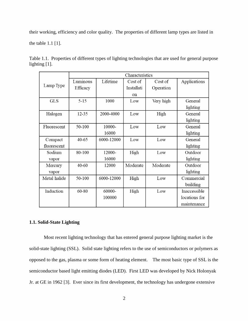
their working, efficiency and color quality. The properties of different lamp types are listed in
the table 1.1 [1].
Table 1.1. Properties of different types of lighting technologies that are used for general purpose
lighting [1].
1.1. Solid-State Lighting
Most recent lighting technology that has entered general purpose lighting market is the
solid-state lighting (SSL). Solid state lighting refers to the use of semiconductors or polymers as
opposed to the gas, plasma or some form of heating element. The most basic type of SSL is the
semiconductor based light emitting diodes (LED). First LED was developed by Nick Holonyak
Jr. at GE in 1962 [3]. Ever since its first development, the technology has undergone extensive

3
research for past three decades and has entered commercial lighting market recently. LEDs are
one of the most efficient and long-lasting lighting technologies. The LED operation temperature
are very low compared to other lighting devices. This allows maximum energy conversion from
electric input into light output and hence has high efficiency. Compared to other lighting
technologies like incandescent or fluorescent lamps, color rendering index of LEDs is low.
Moreover, the operating power is low and lifetime ranges between 25,000-60,000 hours [1].
Initially, red and yellow emitting LEDs were developed and in mid 90s first blue, bright green,
and white emitting LEDs were developed [2].
An LED consists of a p-n junction diode, which is placed on a reflective cavity and
encased inside an epoxy lens. Anode and cathode leads are brought out of the casing for
electrical connections. Figure 1.1 shows the schematic of a LED. The reflective cavity reflects
most of the light emitted from the p-n junction diode and the epoxy lens focuses the emitted light
outward from the top of the LED as shown in figure 1.1
Figure 1.1. Schematic of a solid-state LED chip that is packaged inside a plastic casing. [4]
4
The emissive part of the device is a p-n junction diode. A p-n junction diode is a
semiconductor device that is formed by combining a p-type semiconductor and n-type
semiconductor forming a junction. Semiconductor consists of current carriers namely negatively
charged electrons and positively charged holes. The electrical properties of the semiconductor
directly depend on the free carrier concentration usually expressed per cm3. In an intrinsic
semiconductor the concentration of free electrons is equal to the concentration of holes and is
called the intrinsic carrier concentration. For a given semiconductor intrinsic concentration is a
constant at room temperature. Intrinsic carrier concentration of Si, GaAs and Ge are ~1010, ~106
and ~1013 [5].
For a semiconductor, the valence band [6] and conduction band [6] are separated by a
band gap or forbidden energy gap. The electrons in the valence band are bound and occupy the
lowest energy levels at 0K. Even at higher energies these electrons cannot move within the
valence band as the energy levels are occupied. Instead, these electrons jump into the lowest
levels of conduction band leaving a hole behind when the energy is higher than the band gap
energy. Since the higher levels of the conduction band have kinetic energy, the electrons in the
conduction are free to move. In short, electrons in the valence band can be excited into
conduction band with sufficient energy in form of light, heat, and electric field. The free
electrons in the conduction band and holes in the valence band contribute to the current flow in a
semiconductor device. A p-type semiconductor has excess holes while an n-type semiconductor
has excess electrons when compared to the intrinsic carrier concentration of the semiconductor.
In order to form p-type semiconductor, intrinsic semiconductors are doped with impurity atoms.
The concentration of acceptor dopant atoms (Na) is usually equal to the free hole concentration.
For example, if Si is doped with B, Al or Ga as impurities excess holes are generated turning it
5
into a p-type material [5]. In order to form n-type semiconductor, intrinsic semiconductors are
doped with impurity atoms, which are called donor atoms. The concentration of donor dopant
atoms (Nd) is usually equal to the free electron concentration. Like p-type, if Si is doped with P,
As or N as impurities excess electrons are generated turning it into an n-type material [5]. The
number of dopant atoms introduced per cm3 of the host material determines the doping
concentration. Fermi level (Ef) [7] in an intrinsic semiconductor lies exactly at the middle of the
band gap. For n-type semiconductor free electrons in the conduction band is much higher than
the intrinsic carrier concentration and consequently the fermi level is closer to the conduction
band minimum (Ec). Similarly, in a p-type semiconductor the fermi level is closer to the valence
band maximum (Ev). The position of Ef in a material is critical in determining the electrical
properties of the material. Equations 1.1 and 1.2 are used to calculate the position of Ef in an n-
type and p-type semiconductor, respectively.
EF = EC − KBT logNC
ND (1.1)
EF = EV + KBT logNA
NV (1.2)
where, EF is the fermi level, EC is the conduction band, EV is the valence band, KB is the
Boltzmann constant, T is the absolute temperature, NC is the effective density of states in the
conduction band, ND is the concentration of donor atoms, NV is the effective density of states in
the valence band, NA is the concentration of acceptor atoms.
The band diagram of a p-type and n-type semiconductors are shown in figure 1.2 (a) and
(b). When a junction is formed with these materials, the Ef is continuous as shown in figure 1.2
(c). An energy band diagram with aligned Ef corresponds to the p-n junction in equilibrium or

6
under zero bias. As soon as the junction is formed majority start to diffuse across the junction
and start to recombine leaving a region on either side of the junction called depletion region.
This region consists of uncompensated and immobile donor and acceptor ions. These
uncompensated, separated charges in the junction create an internally built-in electric field,
which in turn results in built-in voltage (Vb) across the junction. This can be seen in figure 1.2(c)
as the difference between the Ec or Ev positions of the energy band diagram, which is in the form
of energy barrier (qVb). The region outside the depletion region is called the charge neutral
region. A simple p-n junction is called a p-n junction diode.
(a) (b)
(c)
Figure 1.2. The band diagram schematics of (a) p-type, (b) n-type and (c) p-n junction are shown
with the EF

7
In the case of a LED, p-n junction diode is forward biased, and charges are injected towards the
junction. The current conduction is minimum initially as there are energy barriers for holes and
electrons as seen in figure 1.2(c). With further increase in forward voltage, the barrier gradually
reduces, and carriers are injected across the junctions. At the same time the equilibrium position
of Ef is split into quasi fermi levels Efp and Efn. During this process electron-hole pairs are
formed that recombine and emit the photon. This is shown in figure 1.3. The energy of the
emitted photon depends on the band gap of the semiconductor and is approximately equal to the
band gap energy value. The voltage at which the LED turns ON is called the turn-on voltage.
This voltage is usually a little over to the Vb of the p-n junction. In case of Si p-n junction Vb is
~0.7 V and this can vary depending on the semiconductor material. Usually, LEDs in the visible
region are made with compound semiconductors and have higher Vb than Si p-n junction. Table
1.2 shows the commonly used semiconductors for different visible light emission.
Figure 1.3. The band bending of the p-n junction energy band under forward bias voltage is
depicted with quasi fermi levels. The process of charge injection across the junction and
recombination are shown.

8
Table 1.2. Commercially available LED colors and corresponding semiconductors used to
produce these colors are listed [8-15].
For general lighting applications lamps that emit natural white light is needed. Humans
perceive white light when all visible wavelengths are combined. Of the visible wavelengths pure
red, green, and blue wavelengths are combined to form the natural white light. Most accurate
white light is rendered by the sunlight and is used as a standard for comparing artificial lights.

9
The relative intensities of these wavelengths must be balanced to by some form of technology to
obtain natural white light. Any imbalance would form a warmer white light, more towards the
red end or cooler white light, more towards the blue end of the visible spectrum. Several
modifications are made to existing LED chips that emit single color to form white light. Discrete
red, green and blue LED chips are encapsulated in a single package and made to emit
trichromatic white light. Dichromatic white light is produced by using blue and yellow emitting
chips. Phosphors are also used to produce white light by acting as color convertors or filters. A
blue or UV LED is used as the emissive part and red, green, yellow and orange phosphors are
encapsulated with it [16]. These phosphors of different colors absorb the high energy blue or
UV light and re-emit lower energy light. This is perceived as the white light. Some of the
schematics of the existing LED white lighting technologies are shown in figure 1.4. Several
advancements were made in LED technology by incorporating nanostructures. As shown in the
figure 1.5, compared to incandescent and fluorescent lamps, white LEDs renders white light
more effectively. The spectrum of commercial white LED is closer to the sun’s spectrum in the
visible region.
(a)

10
(b)
Figure 1.4. (a) White light is generated using blue/UV LED and RGB phosphors or combining
the emission discrete red, green, and blue LEDs in the same package. (b) Cutaway schematic of
phosphor based white LED with yellow phosphor and blue LED.
Figure 1.5. The white light quality of LEDs is compared to sunlight, incandescent and compact
fluorescent lamps [17].
1.1.1 LED parameters
The device characterized by power conversion efficiency, external quantum efficiency
and luminous efficacy. Luminous efficacy of these devices is high around 150 lm/W and it
depends on the type of semiconductor and device architecture [18]. The power conversion

11
efficiency is the ratio of radiant power output to input electric power. The overall conversion
efficiency depends on mechanisms that control carrier injection, carrier recombination, and LED
package. These mechanisms can be combined into an efficiency parameter called external
quantum efficiency given by equation 1.3 [18].
ηext = ηinjηintηout (1.3)
where, ηext is the external quantum efficiency, ηinj is the carrier injection efficiency, ηint is the
internal quantum efficiency, and ηout is the out-coupling efficiency. Some of the best red
emitting AlInGaP and blue emitting InGaN LEDs can have radiative or internal quantum
efficiencies of 100% and 50%, respectively [19]. In order to achieve such high external quantum
efficiencies, light extraction from the package must be improved.
1.2. Thin film LED technologies
1.2.1. Organic LED
This film lighting devices for general lighting and display applications were initially
developed using organic small molecules and polymers [20]. These are called as organic light
emitting diodes (OLED). The technology is so advanced these days that most displays for
devices like televisions, smart phones and other smart devices consist of OLEDs as basic lighting
elements [21]. Some of the major advantages of OLEDs over regular LEDs are that the
manufacturing process is simpler, can be made flexible and large area, and wide variety of
organic emissive materials are available to cover the entire visible spectrum. An OLED consists
of thin films of organic small molecules or polymers that are fabricated in a layer-by-layer
architecture. The device is formed sandwiching a layer of organic emissive material between the

12
anode and cathode. Additionally, charge transport layers (CTL) are introduced between the
emissive layer and electrodes for efficient charge transport [20]. The substrate is glass or other
flexible materials that are coated with transparent conductive oxide (CTO) like indium thin oxide
(ITO) or fluorine tin oxide (FTO). The CTO acts as the anode. Organic small molecule or
polymer based hole transport layer (HTL) is grown on top of the anode. The HTL is followed by
the emissive layer, the electron transport layer (ETL) and the reflective metal cathode. The
schematic of an OLED is shown in figure 1.6. The layers are either spin coated from a solution
or thermally evaporated from a solid source using vacuum deposition [22].
Figure 1.6. The schematic of OLED device that is fabricated on glass substrate by layer-by-layer
deposition.
The emissive material is a π-conjugated organic insulator and carriers must be injected
into it from the electrodes [23]. The injected carriers recombine in the emissive layer and emit
the photon. Unlike semiconductors, the organic layers do not have valence and conduction
bands. They have molecular orbitals and the energy of the emitted photon is approximately
equal to energy separation between highest occupied molecular orbital (HOMO) and lowest
unoccupied molecular orbital (LUMO). These molecular orbitals are analogous to valence and
conduction bands in an inorganic semiconductor. Usually, the barrier to injection of carriers
from the electrodes into the LUMO and HOMO of the emissive layer is high and so injection

13
efficiency is very low. This is overcome by introducing the CTLs, which act as steps for carrier
injection into the emissive layer [20]. For a given emissive layer the ETL is chosen to have its
LUMO level aligned with that of the LUMO of the emissive layer. For efficient hole transport
the HOMO level of the HTL must align with the HOMO of the emissive layer. The barrier to
electron and hole injection must be approximately equal to achieve a balanced charge injection
[24]. If one of the barriers is lower than the other, then an imbalance occurs that leads to
reduction in efficiency [24]. Several organic and inorganic CTLs were investigated to optimize
the performance of OLEDs. Other than the LUMO and HOMO alignment, carrier mobility,
environmental stability, compatibility with the emissive layer, and ease of processing were
considered while choosing the CTLs. Progress in luminous efficacy of different white light
technologies is shown in figure 1.7 [25].
Figure 1.7. Progress in white light technologies with prediction that white OLED reaching a
maximum luminous efficacy of 150 lm/W by 2020 [25].

14
1.2.2. Quantum dot LED
Colloidal quantum dot light emitting diodes (QLED) were recently investigated as a
replacement for the existing OLEDs. The advantages of QLED include high color purity, size
tunable and saturated emission, environmentally stable and low power operation over OLED [26,
27]. In the case of QLED, the organic emissive layer is replaced with inorganic quantum dots
commonly Cd, Se, S and Zn based quantum dots. Quantum dots used for LED devices are
nanostructures of II-VI chalcogenide semiconductors. The size of these quantum dots is between
2-20 nm in diameter [28]. These quantum dots have unique properties when compared to the
bulk properties of the same material due to high surface to volume ratio of these quantum dots.
The band gap of the quantum dots increases with decrease in the size. In the case of CdSe, the
bulk material band gap is ~1.7 eV and increases when it is made into a nanostructure. A
quantum dot provides 3D confinement of excitons as opposed to a bulk material where the
excitons are not confined. An exciton is a bound electron-hole pair and the size of the exciton is
called the exciton Bohr radius [29]. When the exciton Bohr radius is comparable to the size of
the material the confinement is very low. The confinement is strong when the size of the
quantum dot is much smaller than the exciton Bohr radius. In this strong confinement regime,
the energy levels are not continuous instead are quantized. These quantized energy levels relate
quantum dots more closely to atoms than bulk materials. This is a very important property of
quantum dots that make them suitable for use in QLED as efficient emissive materials. The
confinement increases the radiative lifetime of excitons in quantum dots, which increases the
probability of radiative recombination. Additionally, since the emission wavelength of the
QLED is approximately equal to band gap of the quantum dots, it can be controlled by

15
controlling the size of the quantum dots. In other words, same material with different sizes can
by synthesized to emit different wavelengths in the visible spectrum.
Like OLEDs, carriers are injected into the quantum dots from the cathode and anode
through the CTLs. Based on the type of transport materials used, QLEDs are classified into
organic, hybrid organic/inorganic and inorganic. These architectures are schematically
represented in the figure 1.8. Organic QLEDs consists of organic polymers or small molecules
(a) (b) (c)
Figure 1.8. Schematics of (a) organic (b) hybrid and (c) all-inorganic QLED showing the
transport layer and emissive layer are shown
as the CTLs with inorganic quantum dot emissive layer. Some of the commonly used organic
HTLs are poly(3,4-ethylenedioxythiophene) polystyrene sulfonate (PEDOT:PSS), Poly[N,N’-
bis(4-butylphenyl)-N,N’-bisphenylbenzidine] (poly-TPD), poly(N-vinylcarbazole) (PVK),
Tris(4-carbazoyl-9-ylphenyl)amine (TCTA) and N,N′-Di(1-naphthyl)-N,N′-diphenyl-(1,1′-
biphenyl)-4,4′-diamine (α-NPD), 4,4′-Bis(N-carbazolyl)-1,1′-biphenyl (CBP) [22,23]. Of these
the polymers are mostly solution processable, while the small molecules are both solution
processable and can be deposited thermally. Commonly used organic ETLs are 2, 2′,2"-(1,3,5-
Benzinetriyl)-tris(1-phenyl-1-H-benzimidazole) (TPBi), and Tris-(8-hydroxyquinoline)aluminum
(Alq3) [22]. These devices were reported to be operating under direct charge injection, resonant
energy transfer or both [24]. These proposed models are schematically illustrated in figure 1.9.

16
Figure 1.9. Charge transport in QLED is explained using a schematic. The red arrows depict
direct charge injection and green arrows depict the energy transfer mechanism.
In the direct charge injection model, holes are injected into the valence band of the quantum dot
through the HTL and electrons are injected into the conduction band through the ETL. In this
model the transport layers facilitate the injection of carriers by reducing the barrier to carrier
injection, in other words they act as steps to the carriers injected from the electrodes. In the
energy transfer model, excitons are created in the charge transport layers that transfer the energy
non-radiatively to the adjacent quantum dots forming excitons in the quantum dots. First form of
organic QLEDs consisted of CdSe cores-polymer bilayer composites sandwiched between metal
electrodes [30, 31]. These devices exhibited very low external quantum efficiency of <0.5%
with a luminance of 600 cd/m2 [32]. With further research, it was established that a closed pack
monolayer of quantum dot film is required, which will decouple the emission process from the
charge transport process through organic CTLs [33]. Quantum dot dispersions were mixed with
polymer transport layer solution and spun together to form a self-assembled monolayer of
quantum dots on the transport layer. This process is called phase separation, which enhanced the
quantum efficiency of organic QLEDs [27, 33]. Micro contact printing technology was
employed to fabricate organic QLED with external quantum efficiency >2.5% [34].

17
The hybrid QLEDs are the most widely studied and reported, which consists of quantum
dot emissive layer, organic HTL and inorganic ETL. The inorganic ETLs are mostly n-type
metal oxide semiconductors like zinc oxide, titanium dioxide, and tin oxide [35]. The efficiency
of the hybrid devices is reported to be as high as 20% [36-38]. Like organic QLEDs, hybrid
devices are reported to work under both direct charge injection and resonant energy transfer
mechanisms [39]. Qian et al. demonstrated all solution processed hybrid RGB QLEDs with
external quantum efficiencies reaching 0.22%, 1.8% and 1.7% for blue, green and orange-red,
respectively [40]. The quantum efficiencies were further enhanced by using an inverted structure
with a maximum luminance reaching 218,000 cd/m2 for the green QLED [41]. Over 20%
efficient hybrid QLEDs were reported recently [36-38].
In inorganic QLED, all the materials used are inorganic except for the organic ligands
that surround the quantum dots. Commonly used inorganic HTLs are nickel oxide, tungsten
trioxide, vanadium pentoxide, and graphene oxide [26, 42-52]. These inorganic devices are
environmentally more stable and can support higher current densities than similar hybrid devices
with CdSe quantum dots, but these devices are not well developed and quantum efficiency of the
devices are ~1% [42-51]. In general, the external quantum efficiency of QLED is given by
equation 1.4 [53]:
EQE = ηtηocηPLχ (1.4)
where, ηPL is the quantum yield of the CdSe quantum dots, ηt is the charge transport efficiency
of the device, ηoc is the light out-coupling efficiency and χ is the fraction of excitons that have
allowed transitions in the quantum dot. The CdSe quantum dots are well developed and studied
so the χ of these quantum dots are reported to be ~1 [53, 54]. Similarly, the quantum yield of
18
CdSe, specifically alloyed CdSeZnS system is as high as 70% [55-57]. Out-coupling
efficiency,ηoc, is dependent on the device packaging and independent on the device operation.
So, in a QLED device with alloyed CdSe/ZnS quantum dots, the external quantum efficiency is
limited by the charge transport efficiency. In order to improve the efficiency of inorganic
QLEDs, it is necessary to understand the charge transport mechanism and improve the charge
transport efficiency. Most of the reports suggest the that charge transport occurs through direct
charge injection mechanism, while some other report suggest that efficiency of the device is
independent of the charge transport [39, 58, 59]. More specifically, hole (valence band) states in
the quantum dots are between 1.5 – 2 eV higher than they are in the HTL, [42-53] leading to the
accumulation of holes at the interface without the holes ever reaching the quantum dot valence
band. This results in the charging of the quantum dots due to excess electrons reaching the
quantum dot from the cathode, which ultimately reduces the quantum efficiency of the device
due to non-radiative Auger recombination. On the other hand, it is reported that in a QLED
device working with energy transfer mechanism Auger recombination can be suppressed
significantly [39, 53, 60, 61]. For energy transfer to occur, the donor and the acceptor states
need to be in resonance. Commonly used inorganic CTLs have bandgaps greater than 3.0 eV,
well above the band gap of quantum dots emitting in the visible region, so any form of resonant
energy transfer from the valence and conduction band of these CTLs is ruled out. In other
words, there is no spectral overlap between the CTLs’ band edge emission and the quantum dot
absorption. So, new materials, material structures or modifications to existing inorganic HTLs
are required to fabricate an efficient all-inorganic QLED. The progress in the different QLED
architectures is shown in figure 1.10.

19
Figure 1.10. Progress in the performance of QLED architectures over a period of 30 years that
are commonly reported in literature.
1.3. Research Objectives
The goal of this project is to understand the charge transport mechanism, improve the
charge transport efficiency and ultimately increase the quantum efficiency of all-inorganic
quantum dot light emitting devices. The most important efficiency limiting factor is the non-
availability of inorganic HTL that can either support direct charge injection or energy transfer
mechanism. Nickel oxide can be made in the form of thin film and nanoparticles that can
support energy transfer and direct charge injection, respectively. For energy transfer to occur,
the donor (HTL) and the acceptor (quantum dots) states must be in resonance. Commonly used
HTLs have bandgaps greater than 3.0 eV, well above the band gap of quantum dots emitting in
the visible region. Any form of resonant energy transfer from these HTLs is ruled out due to the
non-availability adjacent resonant states in the quantum dots. So, if resonant states are located
within the band gap of the HTLs formed due to defects, energy transfer is possible. It is well
established that nickel oxide is p-type owing to defects in the lattice and that the properties of the

20
thin film can be tuned by varying the growth conditions and post-growth treatments [62-65].
More specifically, the stoichiometry of the film can be controlled by growing nickel oxide in an
oxygen controlled environment [66]. Higher % oxygen leads to the formation non-
stoichiometric nickel oxide with Ni vacancies. This makes nickel oxide an ideal HTL to
investigate the energy transfer mechanism over other HTLs namely V2O5, WO3, and MoO3.
Similarly, nickel oxide nanoparticles can be synthesized that can inject hole more efficiently. By
preparing nickel oxide in the form of nanoparticles, the bandgap and the stoichiometry can be
controlled. This directly affects the position of the valence band and thus enabling direct charge
injection into the quantum dots. This project investigates these two forms of nickel oxide to
improve the efficiency of all-inorganic QLED.
21
2. EXPERIMENTAL PROCEDURES
In this chapter, all material synthesis procedures and characterization tools used in this
project are discussed. In section 1 material synthesis, sample fabrication and device fabrication
procedures are discussed. Under this section, the syntheses of alloyed CdSe/ZnS core /shell
quantum dot, nickel oxide HTL and ZnO nanoparticle ETL are discussed. The bilayer sample,
nickel oxide thin film Schottky diode, ZnO thin film transistor and QLED devices fabrication are
discussed in the second part of section 1. In section 2 the material and device characterization
techniques/tools are discussed.
2.1. Material Synthesis, sample and device fabrication
2.1.1. CdSe/ZnS core shell alloyed quantum dots
The nanocrystals used as the emissive layer in the QLED are CdSe/ZnS alloyed
core/shell nanocrystals. The main advantage of using alloyed core/shell over conventional
core/shell structure is the reduced lattice mismatch between the core and shell [28, 57, 67]. Also,
this structure enables the single step synthesis of the nanocrystals. The synthesis utilizes the
chemical reactivity difference between the cations and anions. The Cd and Se are more reactive
than the Zn and S, which enables the formation of CdSe core first. Once the Cd and Se
precursors are used up in the reactor, the Zn and S starts forming the shell. There is no defined
interface between the core and shell, but the interface is an alloy of CdSeZnS. This is
schematically shown in the figure 2.1(a) and (b). The alloyed core/shell nanocrystals are
synthesized by modifying the procedure reported by Bae, et al. [57, 67]. The synthesis
apparatus, shown in figure 2.1(c) consists of a three-neck flask connected to a Schlenk line
through a condenser tube. The Schlenk line is used to connect the reactor to N2 and vacuum

22
during the reaction. The condenser tube is used to reflux the solvent into the reactor as the
reaction is carried out at over 300 oC. The reactor temperature is controlled by a closed loop
temperature controller setup using a thermocouple sensor and a heating mantle. The heating
mantle is placed on a magnetic spinner to stir the reaction mixture using a magnetic stirrer bar.
The whole setup is placed under a fume hood to remove any volatile and toxic fumes. The main
N2 line of the fume hood and a 20 mTorr vacuum pump are connected to the Schlenk line.
(a) (b)
(c)
Figure 2.1. Schematics of a (a) conventional core/shell quantum dot and (b) alloyed core/shell
quantum dot are depicting the core/shell interface. (c) The core/shell quantum dots are
synthesized using a Schlenk line and three neck flask setups.
To synthesize quantum dots of different sizes two different synthesis approaches were
investigated. In the first approach the precursor concentrations, reaction temperature, time are
kept constant and the ligand concentration is modified. The ligands play the role of controlling
the size of the quantum dot and after synthesis ligands prevent the aggregation of the quantum

23
dots [68]. The cyan emitting (510 nm) quantum dots were synthesized by following the
procedure reported in literature [67]. The growth temperature was 300 oC and the growth time
was 10 min. Other larger quantum dots (green 550nm, yellow 570nm, and red 620nm) were
formed by reducing the ligand concentration. The resulting quantum dots showed a wide size
distribution with a FWHM of more than 50 nm. Moreover, the quantum dot dispersions were
cloudy with precipitates, which would potentially affect the film quality during device
fabrication. For QLED device application, better quality quantum dots with more uniform size
distribution and clear quantum dot dispersions are needed.
In the second approach the ligand concentration, growth temperature, and growth time
were kept constant. Instead, the starting precursor concentration ratios (Cd:Zn:Se:S) were
modified. In a typical single step synthesis, 0.1 mmol of Cadmium oxide and 4 mmol of Zinc
acetate were heated with 17.7 mmol of Oleic acid in a three neck round bottom flask. The
mixture was degassed with a 20 mTorr vacuum at 150 oC for 30 min to remove any volatile
impurities. After 30 min, clear solution mixtures of cadmium and zinc oleate were formed.
After degassing, 15 ml of octadecene was injected into the flask and the temperature was
increased. At 300 oC, 2ml of trioctylphosphine dissolving 0.2 mmol of Se and 3 mmol of S was
injected rapidly into the reactor. The reaction was allowed to continue for 10 min before the
reactor was rapidly cooled down to room temperature. The starting precursor ratio yielded cyan
emitting (533 nm) nanocrystals with a FWHM of 29 nm. By changing the precursor
concentration ratios blue, green, yellow, and orange quantum dots were synthesized. To
synthesize the red quantum dots, Se and S were injected separately [38]. Initially, 0.4 mmol of
Cadmium oxide and 4 mmol of Zinc acetate were heated with 5 ml of Oleic acid in a three neck
round bottom flask. The mixture was degassed at 150 oC for 30 min to remove any volatile
24
impurities. After 30 min, clear solution mixtures of cadmium and zinc oleate were formed.
After degassing, 15 ml of octadecene was injected into the flask and the temperature was
increased. At 300 oC, 2ml of trioctylphosphine dissolving 0.85 mmol of Se was injected swiftly.
The reaction was allowed to continue for 10 min. After 10 min, 1ml of trioctylphosphine
dissolving 1 mmol of S was injected into the reactor. The reactor was cooled to room
temperature after 10 min. The resulting nanocrystals were purified by precipitating with
excessive methanol and hexane. The purification process was repeated at least 3 times before the
nanocrystals were dried and dispersed in hexane at 25 mg/ml concentration for further
experiments. The second approach produced more uniform sized, well dispersed and clear
quantum dot dispersions, which were used in the fabrication of the QLED
2.1.2. Nickel oxide synthesis
Nickel oxide thin films were used as one of the CTLs investigated for hole transport in
all-inorganic QLED. Nickel oxide exists in two forms with Ni having two different oxidation
states Ni2+ and Ni3+. In a stoichiometric nickel oxide (NiO), Ni is present in the form of Ni2+ and
it is a green colored powder. In its non-stoichiometric form (Ni2O3) it appears as a black
powder. Stoichiometric nickel oxide is an insulator and non-stoichiometric form is a p-type
semiconductor with excess holes formed due to Ni vacancies [69]. For hole transport, p-type
semiconductor is required and so non-stoichiometric nickel oxide was synthesized. Two forms
of nickel oxide were investigated namely thin film and nanoparticles.
2.1.2.1. Thin film
Non-stoichiometric nickel oxide thin film was formed by annealing a spin coated layer of
nickel hydroxide at high temperature under ambient atmosphere [50, 62, 63]. First step of the

25
process involved the sol-gel synthesis of nickel hydroxide. Nickel hydroxide was formed by the
hydrolysis of nickel precursor with a weak base. In a typical synthesis, 0.5 M nickel acetate tetra
hydrate solution in ethanol was prepared at room temperature. Once the salt is completely
dissolved, equimolar diethanolamine was added under constant stirring and the reaction was
allowed to continue for 2 hrs at 60 oC on a hot plate. The initial turbid, light green colored
solution turned into a clear, dark green solution indicating the completion of the reaction. Here,
the diethanolamine not only acted as a weak base for hydrolysis, but also made the final solution
more viscous. This enabled the formation of uniform film when spin coated. The bright dark
green colored, clear nickel hydroxide solution is shown in figure 2.2(a). To form the nickel
oxide thin film, the nickel hydroxide sol-gel was spin coated at an optimized speed and annealed
in a box furnace at high temperature under ambient atmosphere. The resulting film exhibited a
pale brownish grey color indicating the non-stoichiometry of the final film. This is shown in
figure 2.2(b).
(a) (b)
Figure 2.2. (a) The dark green and clear nickel hydroxide sol-gel is used as the precursor to the
formation of nickel oxide thin film. (b) Transparency of nickel oxide thin film on glass is
compared to that of a pristine glass slide. “Photo by Ramesh Vasan”

26
2.1.2.2. Nanoparticles
The second form of nickel oxide was the nickel oxide nanoparticle. This was synthesized
by hydrolysis of nickel precursor by a strong inorganic base like sodium hydroxide followed by
high temperature annealing [70]. Initially, 0.5M solution of nickel acetate tetra hydrate in DI
water was prepared at room temperature. To this, freshly prepared 1M solution of sodium
hydroxide in DI water was added dropwise over a 10 min period. The clear green solution turns
into pale green precipitate. The precipitate was collected by centrifugation and the supernatant
solution was discarded. The precipitate was washed 2 to 3 times with DI water and collected by
centrifugation. The purified precipitate was then dried in a box furnace at 80 oC for 2 hrs. The
dried crystals were then ground into a fine powder and annealed at 360 oC for 2 hrs. The
resulting dark brown powder was the nickel oxide nanoparticle. The nanoparticles were then
dispersed in 1-butanol at 20 mg/ml concentration, as shown in figure 2.3, using the ultrasonicator
for further experiments.
Figure 2.3. Nickel oxide nanoparticles are dispersed in butanol for spin coating application.
“Photo by Ramesh Vasan”
2.1.3. Zinc oxide nanoparticles
Zinc oxide nanoparticles were used as the ETL in the QLED devices. Zinc oxide is an n-
type semiconductor with its conduction band position aligning well with the conduction band
CdSe/ZnS alloyed core/shell quantum dots for electron transport [42-52]. Zinc nanoparticles

27
were synthesized by the hydrolysis of zinc acetate dihydrate solution with a strong base [41, 52].
Initially, 0.1M solution of zinc acetate di hydrate in methanol was prepared under room
temperature. To this 0.48 gm of potassium hydroxide dissolved in 25 ml of methanol was added
dropwise inside a N2 filled glove box at 60 oC. The reaction was allowed to continue for 2 hrs to
obtain a white precipitate. The zinc oxide nanoparticles were then washed with excess methanol
and collected. The purification steps were repeated for at least 3 times and the final nanoparticle
precipitate was dried under vacuum to form a white powder. The dried nanoparticles were
dispersed in 1-butanol at 20mg/ml concentration for further experiments.
Figure 2.4. Zinc oxide nanoparticles are dispersed in 1-butanol for spin coating application.
“Photo by Ramesh Vasan”
2.1.4. Quantum dots/nickel oxide thin film bilayer sample
Single layer and quantum dots on glass substrates and quantum dots/nickel oxide thin
film bilayer sample on glass substrates were used to investigate the hole transport mechanism.
Quantum dots dispersed in hexane were spin coated on ultrasonically cleaned glass substrates
and annealed at 80 oC in a N2 glove box to form the single layer sample. For bilayer samples,
quantum dots were spin coated on 60 nm nickel oxide thin film grown on ultrasonically cleaned
glass substrates. The quantum dots/nickel oxide thin film bilayer samples were then annealed at
80 oC in a N2 glove box. The schematics of single layer quantum dot and quantum dot/nickel
oxide bilayer samples are shown in figure 2.5 (a) and (b).

28
(a) (b)
Figure 2.5. Quantum dots are spin coated on (a) pristine glass slide and (b) nickel oxide to
measure the fluorescence lifetime.
2.1.5. Nickel oxide Schottky diode
The electrical properties of the nickel oxide thin film were extracted by analyzing the
electrical characteristics of a Schottky diode. It was fabricated on a 2.5x1.25 cm2 rigid glass
substrate coated with 250 nm of FTO. The sheet resistance of the FTO was measured to be 7–10
Ω/. It consists of an FTO forming an Ohmic contact and Al forming a Schottky contact with
the nickel oxide. The FTO coated glass slide was patterned using adhesive plastic film, zinc
powder, and HCl. The FTO under the plastic film was protected from the HCL, while the FTO
parts exposed to zinc powder were etched away by the HCl. Patterned FTO glass samples were
cleaned successively using DI water, acetone and isopropanol for 30 min each in an ultrasonic
bath. The nickel hydroxide sol-gel was spin coated on cleaned FTO sample and annealed at 400
oC on a hot plate for 10 min to form one layer of nickel oxide. The thickness of the nickel oxide
film was ~100 nm. Two more layers of nickel oxide were formed using the same procedure.
Final annealing was performed in a box furnace at 500 oC for 30 mins to form a ~300 nm nickel
oxide film. On top of the nickel oxide, 100nm Al metal was evaporated using an electron beam
evaporator through a shadow mask forming an active area of 0.1cm2. The evaporator chamber
was maintained at a vacuum of 2e-6 Torr while deposition. The schematic of the FTO/NiO/Al
Schottky diode is shown in figure 2.6.
29
Figure 2.6. A Schottky diode using nickel oxide is fabricated to extract the electrical properties
of the nickel oxide.
2.1.6. Thin film transistor
The mobility of the zinc oxide nanoparticles was calculated from the electrical
characteristics of a thin film transistor with the nanoparticles in the channel [41, 52, 71, 72]. The
transistor consists of a p-type Si sample with a 100 nm SiO2 thermal oxide, which acted as the
gate oxide. A bottom gate thin film transistor was used with source and drain electrodes formed
on the gate oxide using standard photolithography procedure. The channel was formed by the
interdigital electrodes with pads that formed the source and drain. The channel length and width
were 50 µm and 1000 µm, respectively. The top source, drain and bottom gate electrodes were
formed by depositing 100 nm Ag using an electron beam evaporator. The schematic of the thin
film transistor is shown in figure 2.7. Zinc oxide nanoparticles dispersion in 1-butanol was spin
coated on to the channel that was formed by the interdigital electrodes. The pads were cleaned
gently to make contacts by using wedge wire bonding technique. To make contact to the bottom
gate electrode, the sample was made to contact an Au coated substrate using molten In. Gold
wire was wedge bonded to the Au substrate to make contact with the gate electrode.
30
Figure 2.7. A thin film transistor with a bottom gate architecture and zinc oxide nanoparticle
channel is fabricated to calculate the electron mobility in zinc oxide ETL.
2.1.7. QLED devices fabrication
The QLED devices were fabricated on a 2.5x1.25 cm2 rigid glass substrate coated with
250 nm of FTO. The sheet resistance of the FTO was measured to be 7–10 Ω/. The FTO
coating was partly etched using zinc powder and concentrated HCl. The FTO was partly
covered with adhesive plastic tape and the parts exposed to zinc powder were etched away by
HCl. Patterned FTO slides were cleaned in an ultrasonic bath successively using DI water,
acetone, and isopropanol for 30 min each. For the all-inorganic QLED, the nickel hydroxide
precursor sol-gel was spin coated on the cleaned, patterned slides and annealed in a box furnace
at an optimized temperature to form the nickel oxide HTL. For the hybrid QLED device, the
nickel oxide thin film is replaced with PEDOT: PSS hole injection layer (HIL)/nickel oxide
nanoparticle HTL. The HIL/HTL layers were spin coated on cleaned FTO at 5000 rpm for 30 s
and annealed under ambient atmosphere. For both device structures quantum dots dispersed in
hexane was spin coated on the HTL at 2000 rpm and annealed inside a N2 glove box at 80 oC for
30 min. The zinc oxide nanoparticle ETLs was spin coated at 2000 rpm and annealed on a hot

31
plate inside a N2 glove box. The optimized coating speed and annealing temperature enabled the
formation of uniform films. Finally, 80 nm Al cathode was deposited using an electron beam
evaporator through a shadow mask at a vacuum of 1e-6 Torr. The shadow mask was designed
such that the active emissive area of the device formed was 0.15cm2. The schematics of the all-
inorganic and hybrid QLEDs are shown in figure 2.8 (a) and (b) [50].
(a) (b)
Figure 2.8. Schematics of (a) all-inorganic and (b) hybrid QLEDs that are fabricated using a
layer-by-layer deposition technique. Reprinted with permission from Vasan et. al. [50].
2.2. Characterization tools
2.2.1. UV-Vis spectroscopy
UV-Vis spectrophotometry was utilized to measure the absorbance and transmittance of
different materials in this project. A Cary 500 UV-Vis-NIR spectrophotometer was used to
acquire the absorbance and transmission measurements. The range of wavelengths that can be
measured is 175-3300 nm. It consists of a photomultiplier tube detector for UV-Vis region and a
PbS detector for the infrared region. For liquid samples, a Spectrosil® Far UV Quartz cuvette
with a range of 170 to 2700 nm and 1 cm path length was used. For measuring thin films, a
sample holder with double sided adhesive tape was used. The bandgaps of the alloyed CdSe/ZnS
quantum dots, nickel oxide thin film, and zinc oxide nanoparticles were calculated from the

32
absorbance spectrum. The position of the excitonic peak in eV observed in the absorbance
spectra of these materials is approximately equal to the band gap of the material. Absorbance is
calculated by using the Beer-Lambert law, which is given by equation 2.1.
I = I0 e−αd (2.1)
where, I the intensity of the light transmitted through the material, I0 is the incident light
intensity, α is the absorption coefficient, and d is the path length optical density of the material.
Absorption coefficient is a material characteristic and is usually expressed with units of cm-1 and
αd=ln (I0/I) is the absorbance with arbitrary units.
Transmittance of the nickel oxide HTL is an important parameter as the light emitted
from the quantum dot active layer must be transmitted out without absorption. Transmittance is
usually expressed as % of incident light. If none of the incident light is absorbed, it means the
transmittance is 100% and if all the light is absorbed then the transmittance is 0%.
Transmittance is given by equation 2.2.
%T = (I
I0) × 100 (2.2)
Nickel oxide thin film was grown on a rigid glass substrate and hence glass transmittance was
used as a baseline.
2.2.2. Luminescence
Luminescence is defined as the radiative recombination of excitons formed due to excited
carriers. The radiative recombination competes with the non-radiative recombination processes
and must dominate to produce considerable luminescence. In this project photoluminescence
and electroluminescence measurements were used to characterize materials and devices,

33
respectively. For luminescence to occur, non-equilibrium carrier concentration is required in the
electronic bands. If this non-equilibrium is produced by optical excitation then the luminescence
is called photoluminescence and if it is produce electronically be injecting carriers across a p-n
junction, then it is electroluminescence. Other types like sonoluminescence, bioluminescence,
chemiluminescence, cathodoluminescence, thermoluminescence, radio luminescence,
triboluminescence are also possible.
In this project photoluminescence of all the materials used were measured to know the
quality of the materials prior to device fabrication. The spectrum peak is approximately equal to
the band gap of the material. Additionally, photoluminescence spectra of quantum dots can be
used to determine the size distribution of the synthesized quantum dots. A narrow full width at
half max (FWHM) indicates a narrow size distribution, which leads to pure color emission when
in a device. In the case of electroluminescence, the increase in device emission intensity with
bias voltage or injection is recorded as a function of wavelength. Like photoluminescence, the
FWHM of spectrum is used to determine the color purity of the emission. The
Photoluminescence and electroluminescence measurements at room temperature were performed
using a Horiba LabRAM spectrophotometer equipped with Synapse CCD detector. The detector
is a 1024x256 front illuminated Si CCD with a gain setting of 2.55 e-/count. The CCD chip is
electronically cooled to -70oC during measurement. For photoluminescence the excitation was
achieved by a 473 nm continuous laser. The incident laser power is controlled by five neutral
density filters selectable using the spectrometer software. The laser is focused on to the sample
by 50x objective lens and 40 μm slit. The emitted photons from the sample is directed towards
the detector through a vis-IR band pass filter and a 500 nm laser cut-off filter. For
electroluminescence, the QLED device was biased using a 2400 Keithley source meter with a

34
current compliance of 1 A and the emission intensity was measured using the same spectrometer
setup as the photoluminescence. A 10x objective lens and 500 μm slit width were used for the
electroluminescence measurements.
2.2.3. Time resolved photoluminescence
Time resolved photoluminescence is a contactless technique to characterize the carrier
recombination rates and transport properties of semiconductor materials for device applications.
The measurement involves exciting the sample with short pulse laser usually on the ps or fs scale
and subsequently measuring the photoluminescence decay as a function of time. The exciting
source is picosecond or femtosecond pulsed laser and the detector is a photodiode with streak
camera for time correlated single photon counting. Other filters, monochromator, optics, pin
holes are used within the system. Time resolved photoluminescence using time-correlated single
photon counting is used for II-VI quantum dot carrier dynamics as the time scales are in the
nanosecond scales.
In this project lifetimes were measured using a MicroTime 200 scanning confocal
fluorescence microscope (PicoQuant GmbH, Berlin, Germany), which is based on Olympus
IX71 equipped with PicoHarp 300 TCSPC controller [73, 74]. It utilizes a 485 nm laser (PDL
485, Picoquant) operating in pulsed wave mode at a power of ~0.05 μW and a repetition rate of 4
MHz for excitation. A dichroic mirror (500dcxr, Chroma, McHenry, IL) sends the light through
a water immersion objective (Olympus, Apochromat 60x, NA 1.3) to a diffraction-limited laser
focus. The same objective collects the fluorescence and sends it through the same dichroic mirror
and a 50 μm pinhole. To reject background fluorescence and scattered laser light, a fluorescence
filter that best matches the emission wavelength of the quantum dots (HQ520/35M for blue

35
quantum dots with emission peak at 495 nm, HQ520/35M for cyan quantum dots with emission
peak at 530 nm, HQ560/40M for green quantum dots with emission peak at 550 nm,
HQ585/40M for yellow quantum dots with emission peak at 580 nm, HQ605/55M for orange
quantum dots with emission peak at 600 nm) was placed in front of the Single Photon Avalanche
Diode Detector (SPAD, MPI, Microphotonic devices, Bolano, Italy). The photons are binned
using the TCSPC card into 64 ps channels for fluorescence lifetime analysis and the fluorescence
lifetime curves were then analyzed using the freely downloadable program DecayFit
(Fluorescence Decay Analysis Software 1.3, FluorTools, www.fluortools.com) using the
instrument IRF for iterative reconvolution fitting.
2.2.4. Current-Voltage Characteristics
Current-Voltage characteristics were measured using a Keithley 4200 semiconductor
characterization system equipped with two source measure units (SMU) with 4200-PA pre-
amplifiers. The preamplifiers extend the resolution of the SMUs to 0.1 fA. The two SMUs were
used simultaneously to force and sense. Also, the Keithley Model 8101-TrX PIV test fixture was
used to perform four probe measurements with just two SMUs. In this project the current-
voltage characteristics of FTO/NiO/Al Schottky diode, the QLED, and zinc oxide thin film
transistor were measured using this system. The Schottky diode and QLED measurements were
performed using a built-in 2-wire forward bias diode test module. Source measure unit 1 was
connected to the device anode and was programmed to force and measure. The anode voltage
was swept from 0 to 10V and current was measured simultaneously. Source measure unit 2
connect to the cathode of the device was programmed to be the common. The characteristics of
thin film transistor were measured by setting up a user 3-wire test module. In this, the gate
voltage was swept with SMU 1 and the gate current was not measured. The drain voltage was
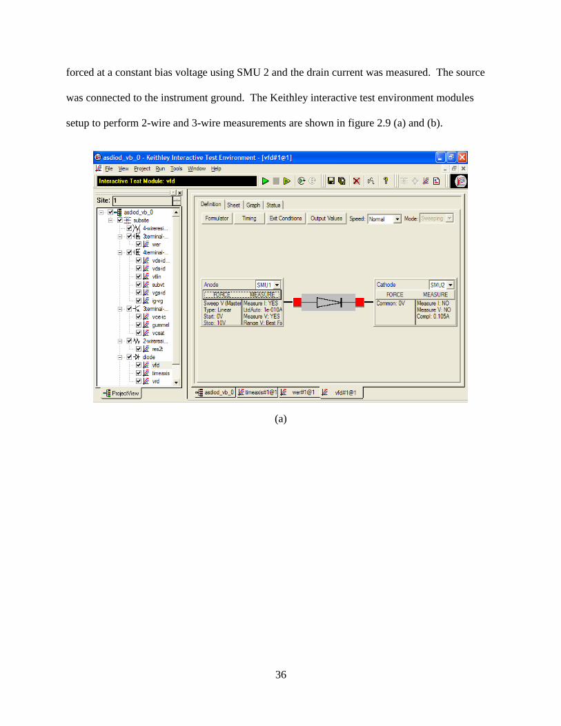
36
forced at a constant bias voltage using SMU 2 and the drain current was measured. The source
was connected to the instrument ground. The Keithley interactive test environment modules
setup to perform 2-wire and 3-wire measurements are shown in figure 2.9 (a) and (b).
(a)

37
(b)
Figure 2.9. Screenshots of the Keithley test modules used for (a) 2 wire and (b) 3 wire device
measurements.
2.2.5. Raman spectroscopy
The basic principle of Raman spectroscopy is that when a laser light is incident on the
sample, the light is scattered inelastically by the optical phonons. The spectral distribution of the
scattered light is compared with respect to the incident light. The intensity of inelastically
scattered light is few orders of magnitude smaller than the elastically scattered light. So it is
important that the elastically scattered light is filtered using an appropriate notch filter to detect
the inelastically scattered light accurately. Other than optical phonons, incident light can also be
scattered by quasi particles like optical magnons, plasmons and even electronic excitations [75].
The light can be shifted to higher energy as in anti-Stokes shift or lower energy as in Stokes
shift. A schematic of Raman scattering mechanism is shown in figure 2.10.
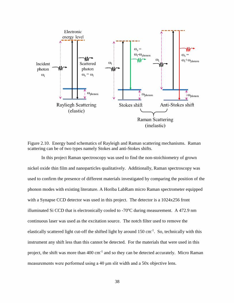
38
Figure 2.10. Energy band schematics of Rayleigh and Raman scattering mechanisms. Raman
scattering can be of two types namely Stokes and anti-Stokes shifts.
In this project Raman spectroscopy was used to find the non-stoichiometry of grown
nickel oxide thin film and nanoparticles qualitatively. Additionally, Raman spectroscopy was
used to confirm the presence of different materials investigated by comparing the position of the
phonon modes with existing literature. A Horiba LabRam micro Raman spectrometer equipped
with a Synapse CCD detector was used in this project. The detector is a 1024x256 front
illuminated Si CCD that is electronically cooled to -70oC during measurement. A 472.9 nm
continuous laser was used as the excitation source. The notch filter used to remove the
elastically scattered light cut-off the shifted light by around 150 cm-1. So, technically with this
instrument any shift less than this cannot be detected. For the materials that were used in this
project, the shift was more than 400 cm-1 and so they can be detected accurately. Micro Raman
measurements were performed using a 40 μm slit width and a 50x objective lens.

39
2.2.6. X-ray Diffraction
X-ray Diffraction (XRD) is a contact less material characterization technique used to
identify elements, lattice spacing, crystal structures, and crystal orientation. In a crystalline
structure, atoms are arranged in a periodic three-dimensional lattice. The space between two
adjacent lattice point is called the lattice constant of the crystal. When a beam of high energy x-
ray is incident on a crystal, they are scattered elastically from different planes of the crystal. This
is called Thomson scattering. In this process the electrons oscillate at the same frequency of the
incoming x-ray beam. The scattered x-ray beams from different lattice planes undergo
interference, which are recorded as diffraction pattern. The spacing and intensity of the
diffraction pattern are analyzed to determine crystal structure and identify elements. The patterns
are analyzed using Bragg’s law according to equation 2.3.
2d sin θ = nλ (2.3)
where, n is a positive integer and λ is the wavelength of the incident wave, d is the distance
between the diffracting lattice planes, and θ is the scattering angle.
In this project XRD measurements were performed to optimize the annealing
temperature, time, and environment to obtain nickel oxide thin film with large gain size.
Additionally, XRD measurements were utilized to check for non-stoichiometry and crystallinity
of charge transport layers used in this project. The samples were measured using Philips PW
3040 X’PERT MRD High Resolution XRD.

40
2.2.7. X-ray Photoelectron Spectroscopy
X-ray photoelectron spectroscopy (XPS) is a non-destructive material characterization
technique used to determine the elemental composition, chemical and electronic states in a
material. In this, high energy x-rays are used as an excitation source and inner shell electrons are
ejected out of the sample by Auger process or by photoemission process. The kinetic energy of
the ejected electron is detected, and properties of the material are determined. The electron
energy is raised to the detector level and need not be raised to vacuum level. In Auger process,
an excited electron recombines with a hole and the energy is transferred to another electron,
which gets ejected out of the material. The energy of the released electron is approximately
equal to the recombination energy. In photoelectron spectroscopy, a hole is left releasing the
electron form the core or valence levels. In this case the kinetic energy of the released electron is
measured instead of the Auger process or the recombination energy. The Auger and
photoemission processes are schematically represented in figure 2.11. In XPS, high energy
Figure 2.11. Auger and photoemission are the processes associated with X-ray photoelectron
spectroscopy.
x-rays strike the surface of the material and penetrate the surface to about 10-20 nm. The kinetic
energy of the emitted electrons is used to calculate the binding energy of the electrons to the core
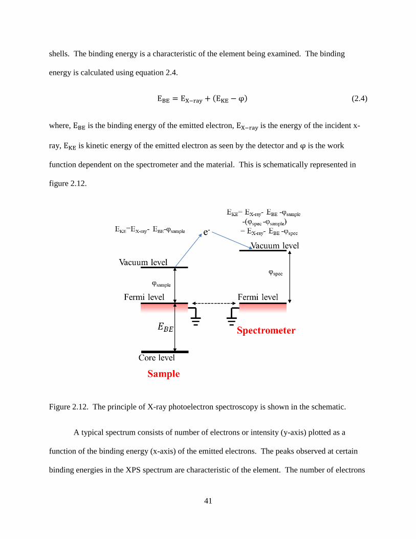
41
shells. The binding energy is a characteristic of the element being examined. The binding
energy is calculated using equation 2.4.
EBE = EX−ray + (EKE − φ) (2.4)
where, EBE is the binding energy of the emitted electron, EX−ray is the energy of the incident x-
ray, EKE is kinetic energy of the emitted electron as seen by the detector and φ is the work
function dependent on the spectrometer and the material. This is schematically represented in
figure 2.12.
Figure 2.12. The principle of X-ray photoelectron spectroscopy is shown in the schematic.
A typical spectrum consists of number of electrons or intensity (y-axis) plotted as a
function of the binding energy (x-axis) of the emitted electrons. The peaks observed at certain
binding energies in the XPS spectrum are characteristic of the element. The number of electrons

42
in each of the characteristic peaks is directly related to the amount of element within the
material. In a typical system, a monochromatic Al kα X-rays are produced by focusing a beam
of electrons on to an Al disk. The resulting Al kα X-rays have an energy of 1486.7 eV [76]. The
X-rays are focused on the sample loaded on to an ultra-high vacuum chamber (<10-9 mb). The
emitted core electrons are then directed toward the electron analyzer and electron detector to
record the binding the energy and intensity, respectively.
2.2.8. Atomic Force Microscope
Atomic Force Microscope (AFM) is a scanning probe microscopic technique used to
image the topographical features of samples that can be conductive or insulating. It is more
advantageous to use AFM over electron microscopes for topographical imaging as the sample
need not be electrically conductive. It consists of a pyramid shaped probe that is 3-6 µm in
length with a tip diameter 0f ~25 nm, and AFM measures the force between the force and the
sample surface. The probe is mounted at the end of a cantilever that is made of silicon or silicon
nitride. To measure the surface features of the sample the cantilever tip is rastered across the
sample continuously or intermittently and the deflection of the cantilever from the surface
feature is monitored. Most common to measure the deflection is to reflect a laser from the
cantilever on to a four-segment photo sensitive photodiode [77]. A simple schematic of an AFM
is shown in figure. AFM operate in three different modes namely, contact mode, tapping mode
and non-contact mode. In contact mode, the probe tip is contacted to the sample surface and
dragged across forming the topographical image of the surface. The main disadvantage of this is
the artifacts created due to damage of the probe or the surface caused by attractive forces. To
overcome this tapping mode is widely used for high resolution images without the limitations of
the contact mode. The cantilever is made to oscillate at a frequency close to the resonant
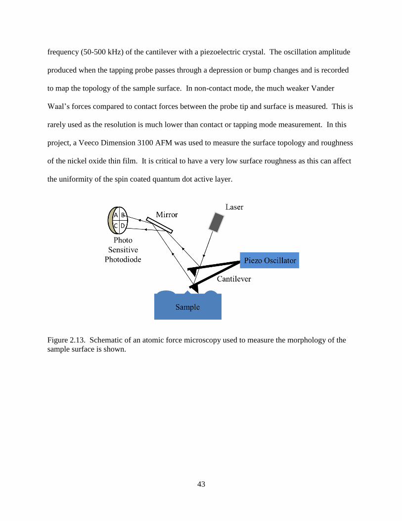
43
frequency (50-500 kHz) of the cantilever with a piezoelectric crystal. The oscillation amplitude
produced when the tapping probe passes through a depression or bump changes and is recorded
to map the topology of the sample surface. In non-contact mode, the much weaker Vander
Waal’s forces compared to contact forces between the probe tip and surface is measured. This is
rarely used as the resolution is much lower than contact or tapping mode measurement. In this
project, a Veeco Dimension 3100 AFM was used to measure the surface topology and roughness
of the nickel oxide thin film. It is critical to have a very low surface roughness as this can affect
the uniformity of the spin coated quantum dot active layer.
Figure 2.13. Schematic of an atomic force microscopy used to measure the morphology of the
sample surface is shown.
44
3. RESULTS AND DISCUSSION
In this chapter, the first section discusses the material characterization results of
CdSe/ZnS alloyed core/shell quantum dots, nickel oxide thin, nickel oxide nanoparticles and zinc
oxide nanoparticles. Second section explains the results of the quantum dot-nickel oxide bilayer
samples and the proposed charge transport models. In the final section, the device
characterization results of QLED fabricated using nickel oxide thin film and nickel oxide
nanoparticle as HTLs are discussed in detail.
3.1. Material Characterization
3.1.1. CdSe/ZnS alloyed core/shell quantum dots
3.1.1.1. Optical Properties
The CdSe/ZnS alloyed core/shell quantum dots were synthesized using two different
procedures. In the first procedure, the ligand concentration is changed keeping the precursor
concentration, reaction time, and reaction temperature constant. As soon as the Se and S are
injected into the reactor, the Cd and Se start to react first and starts to nucleate. By changing the
ligand concentration, the initial core growth can be controlled, which controls the bandgap of the
final quantum dots. For the cyan quantum dots the initial ligand concentration is 17.7 mmol. In
order to synthesize larger quantum dots with lower gaps the starting ligand concentration is
reduced there by allowing the cores to grow larger. The photoluminescence spectra of different
sized quantum dots synthesized by changing ligand concentration are shown in figure 3.1 (a) and
(b). The FWHM of the cyan, green, yellow, orange and red quantum dots are 40, 50, 48, 52 and
46 nm, respectively. This indicates that quantum dots have a slightly wider size distribution,
when compared to some reported results [57]. The absorbance spectra of the quantum dots are

45
shown in figure. Similar to photoluminescence spectra, the wide excitonic peak indicates a
wider size distribution. The final quantum dot dispersions formed using this method are cloudy,
which affects the uniformity and quality of the spin coated emissive layer.
The optical properties of the CdSe/ZnS alloyed core/shell quantum dots that were
synthesized by changing the precursor concentration ratios are plotted in figure 3.1 (c) and (d).
The FWHM of the photoluminescence spectra of blue, cyan, green, yellow, orange and red
quantum dots are 29, 29, 30, 40, 45 and 34 nm, respectively. The narrow size distribution is
advantageous in a device as the emission color will be pure and saturated. The band gap and size
of the quantum dots are calculated using the excitonic peak seen in the absorbance spectra shown
in figure. Compared to the previous procedure, this procedure produced quantum dots that are
completely dispersible in hexane and form clear solutions. The quantum dot dispersions under
the UV illumination is shown in figure 3.1 (e) and (f). The precursor concentration, PL peak,
bandgap and size of the quantum dots are tabulated in table.
(a) (b)

46
(c) (d)
(e) (f)
Figure 3.1. Optical properties of alloyed quantum dots synthesized by changing the ligand
concentration are evaluated using (a) photoluminescence and (b) absorbance spectra. Reprinted
with permission from Vasan et. al. [50]. Optical properties of alloyed quantum dots synthesized
by changing the precursor concentration are evaluated using (c) photoluminescence and (d)
absorbance spectra. Quantum dot dispersions under (e) white light and (f) UV light.
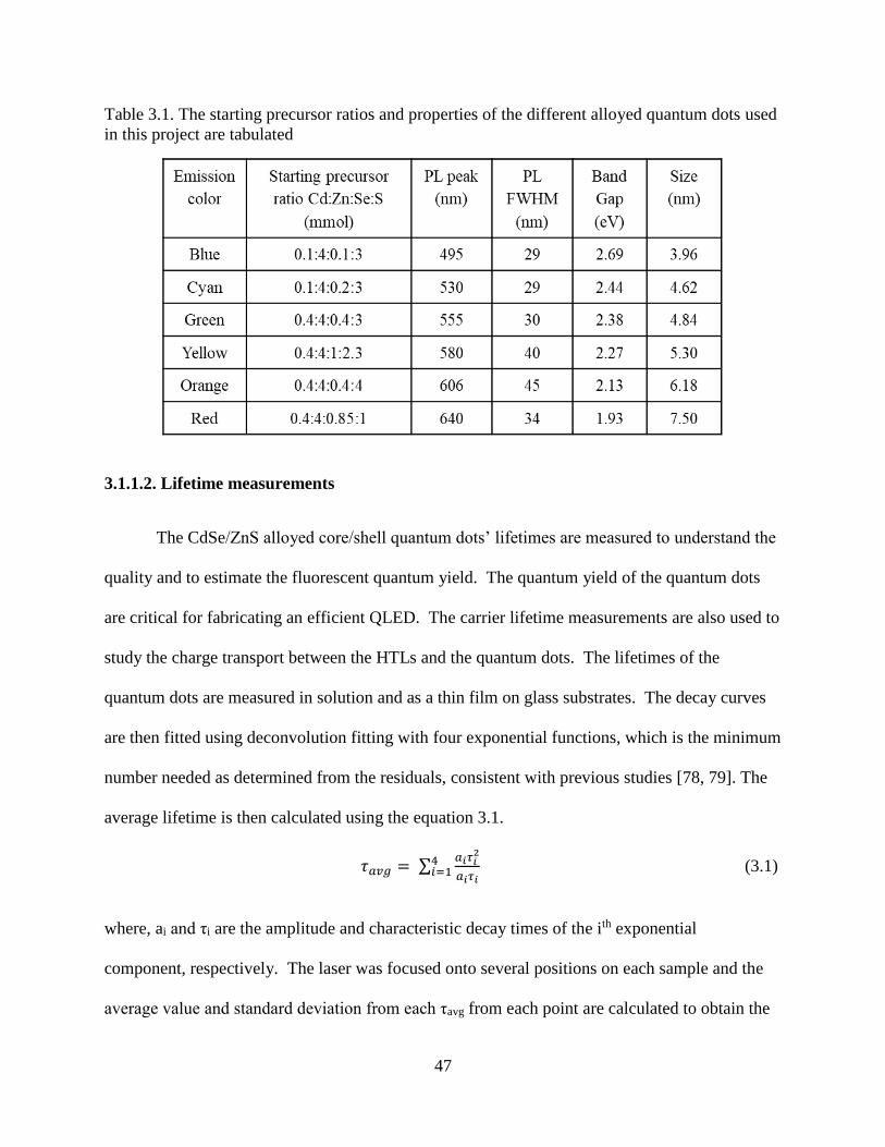
47
Table 3.1. The starting precursor ratios and properties of the different alloyed quantum dots used
in this project are tabulated
3.1.1.2. Lifetime measurements
The CdSe/ZnS alloyed core/shell quantum dots’ lifetimes are measured to understand the
quality and to estimate the fluorescent quantum yield. The quantum yield of the quantum dots
are critical for fabricating an efficient QLED. The carrier lifetime measurements are also used to
study the charge transport between the HTLs and the quantum dots. The lifetimes of the
quantum dots are measured in solution and as a thin film on glass substrates. The decay curves
are then fitted using deconvolution fitting with four exponential functions, which is the minimum
number needed as determined from the residuals, consistent with previous studies [78, 79]. The
average lifetime is then calculated using the equation 3.1.
𝜏𝑎𝑣𝑔 = ∑𝑎𝑖𝜏𝑖
2
𝑎𝑖𝜏𝑖
4𝑖=1 (3.1)
where, ai and τi are the amplitude and characteristic decay times of the ith exponential
component, respectively. The laser was focused onto several positions on each sample and the
average value and standard deviation from each τavg from each point are calculated to obtain the
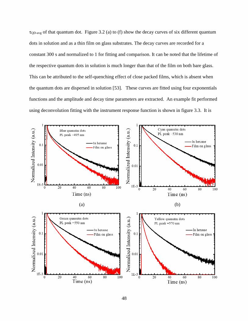
48
τQD-avg of that quantum dot. Figure 3.2 (a) to (f) show the decay curves of six different quantum
dots in solution and as a thin film on glass substrates. The decay curves are recorded for a
constant 300 s and normalized to 1 for fitting and comparison. It can be noted that the lifetime of
the respective quantum dots in solution is much longer than that of the film on both bare glass.
This can be attributed to the self-quenching effect of close packed films, which is absent when
the quantum dots are dispersed in solution [53]. These curves are fitted using four exponentials
functions and the amplitude and decay time parameters are extracted. An example fit performed
using deconvolution fitting with the instrument response function is shown in figure 3.3. It is
(a) (b)

49
(c) (d)
(e) (f)
Figure 3.2. Lifetime decay curves of alloyed quantum dots that are measured in solution and as a
spin coated film on glass.
clear from the figure 3.3 that the fitting is good with very low residuals. So, the average lifetime
of carriers calculated using this fit is accurate and the values are tabulated in table 3.2.
Figure 3.3. Sample decay curve fit using reconvolution fitting method plotted with original
decay curve and instrument response function. The residuals of the fitting are plotted in the
inset.
0 20 40 60 80 1000.0
0.2
0.4
0.6
0.8
1.0
Decay Curve
Fit
Intrument response function
Norm
aliz
ed I
nte
nsi
ty (
a.u.)
Time (ns)
10 20 30 40 50 60 70 80 90 100-0.05
-0.04
-0.03
-0.02
-0.01
0.00
0.01
0.02
0.03
0.04
0.05
Res
idu
als
Time (ns)
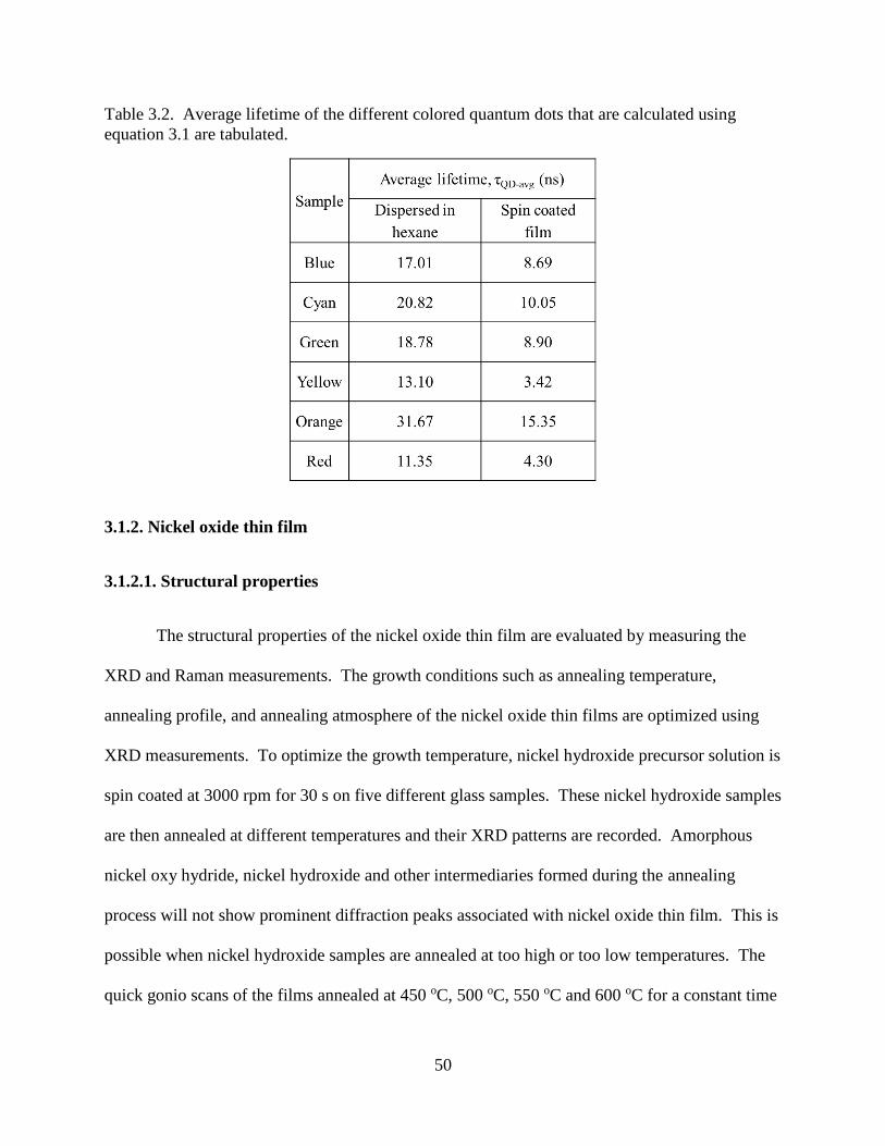
50
Table 3.2. Average lifetime of the different colored quantum dots that are calculated using
equation 3.1 are tabulated.
3.1.2. Nickel oxide thin film
3.1.2.1. Structural properties
The structural properties of the nickel oxide thin film are evaluated by measuring the
XRD and Raman measurements. The growth conditions such as annealing temperature,
annealing profile, and annealing atmosphere of the nickel oxide thin films are optimized using
XRD measurements. To optimize the growth temperature, nickel hydroxide precursor solution is
spin coated at 3000 rpm for 30 s on five different glass samples. These nickel hydroxide samples
are then annealed at different temperatures and their XRD patterns are recorded. Amorphous
nickel oxy hydride, nickel hydroxide and other intermediaries formed during the annealing
process will not show prominent diffraction peaks associated with nickel oxide thin film. This is
possible when nickel hydroxide samples are annealed at too high or too low temperatures. The
quick gonio scans of the films annealed at 450 oC, 500 oC, 550 oC and 600 oC for a constant time

51
of 20 min show characteristic peaks of nickel oxide at 37o and 43.2o. This is shown in figure 3.4
(a). As seen in the figure the nickel hydroxide films annealed at 500 oC and 550 oC exhibit
relatively strong peaks corresponding to nickel oxide, while at 450 oC and 600 oC the peaks show
reduced intensities. So, the optimal annealing time and temperature is 20 min and 500 oC,
respectively. Next, the annealing atmosphere is controlled to deduce the effect of oxygen during
the annealing process. This is critical as the stoichiometry of the final nickel oxide film is
strongly dependent on the oxygen concentration. So, two nickel oxide samples are prepared at
the optimized conditions under ambient air in a box furnace and under vacuum in a tube furnace.
The XRD patterns of the two samples are shown in figure 3.4 (b). It is clear that the nickel oxide
sample annealed under ambient air shows much better crystallinity than the sample annealed
under vacuum. This is evident from the stronger characteristic nickel oxide diffraction peaks at
37o and 43.2o. The sample that is annealed at 500 oC for 20 min in the ambient atmosphere is
polycrystalline with a grain size ranging around 8-9 nm. The grain size is calculated using the
Scherrer’s as shown in equation 3.2.
d =Kλ
βθ (3.2)
where, d is the grain size or crystallite size, K is the dimensionless quantity equal to unity, 𝜆 is
the wavelength of the incident X-ray, which is equal to 1.54 Å (Cu kα line), β is the FWHM of a
diffraction plane, and θ is the Bragg angle. The annealing process is further optimized to
increase the grain size and thereby reduce the scattering due to these grain boundaries. To
achieve this five nickel hydroxide samples are annealed at different annealing profiles to increase
the grain size. First four samples are annealed inside a box furnace and the last sample is
annealed on a hot plate. The annealing profiles are as follows,

52
Sample 1: 0 - 400 oC @10 oC per min, 400 – 500 oC @33.3 oC per min, soak for 20mins @500
oC, ramp down naturally.
Sample 2: 0 - 400 oC @10 oC per min, 400 – 500 oC @25 oC per min, soak for 20mins @500 oC,
ramp down naturally.
Sample 3: 0 - 400 oC @25 oC per min, 400 – 500 oC @25 oC per min, soak for 20mins @500 oC,
ramp down naturally.
Sample 4: 0 - 400 oC @25 oC per min, 400 – 500 oC @33.3 oC per min, soak for 20mins @500
oC, ramp down naturally.
Sample 5: 0 - 500 oC on a hot plate, ramp up and ramp down naturally.
The XRD patterns of these samples are shown in figure 3.4 (c). The gran size of the samples that
are calculated using Scherrer’s equation are tabulated in table 3.3. The plane at 43.2o is used to
calculate the d in nm. The FWHM is obtained by fitting the diffraction plane centered at 43.2o
using a Voigt fit. It is clear from these experiments that the nickel hydroxide samples annealed
in a box furnace with an initial ramp rate of 25 oC per min, a final ramp rate of 33.33 oC between
400-500 oC, annealing time (soak time) of 20 min in ambient air produced the required
polycrystalline thin film of nickel oxide.

53
(a) (b)
(c)
Figure 3.4. The annealing conditions of nickel oxide thin film are optimized using XRD
measurements.
Table 3.3. The grain size of polycrystalline nickel oxide thin film formed using different
annealing profiles calculated using Scherrer’s equation

54
The sotichiometry of the nickel oxide formed utilizing the above optimal processing
conditions is further investigated using XRD measurements. A detailed grazing angle scan of
the nickel oxide film is shown in figure 3.5. The diffraction peaks at 37.2o, 43.3o, and 63.9o
correspond to (111), (200), and (220) planes of the non-stoichiometric nickel oxide [52, 62]. The
positions of the diffraction peaks for stoichiometric nickel oxide (JCPDS card no: 01-089-7130)
are also referenced by vertical lines in figure 3.5. When compared to the crystalline nickel oxide
pattern referenced in the figure, the patterns are broad indicative of smaller grain size and high
defect densities. The position and relative intensity of the XRD pattern of the measured nickel
oxide film also strongly indicate that the film is non-stoichiometric with Ni vacancies. The
position of the peak corresponding to diffracting planes (111), (200), and (220) are shifted to
higher 2θ. The peak for (200) plane is shifted by 0.4o from 42.9o for the stoichiometric nickel
oxide to 43.35o for the non-stoichiometric nickel oxide. Similarly, (111) and (220) are shifted by
0.21o and 0.45o, respectively. Vacancies can also reduce the intensities of the diffracting planes.
The highest intensity peak at 43.35o is taken as the reference and relative intensities of the other
peaks are calculated. The (220) plane peak is 34.1% of the reference intensity, which is lower
compared to stoichiometric nickel oxide. Both the peak shift and intensity reduction are due to
the presence of defect in the form of Ni vacancies and O interstitials [80].

55
Figure 3.5. The crystallinity of solution processed non-stoichiometric nickel oxide HTL is
determined from the XRD measurement. The diffracting planes (111), (200), and (222) of non-
stoichiometric nickel oxide are indexed and compared to the stoichiometric nickel oxide (JCPDS
card no: 01-089-7130).
The structural properties of non-stoichiometric nickel oxide are further evaluated using
Raman spectroscopy. The Raman spectrum, recorded in the range of 300-1500 cm-1, is shown in
figure 3.6. The Raman mode at 560 cm-1 is a LO mode while the mode at 1100 cm-1 is a 2LO
mode. The characteristic LO mode for stoichiometric nickel oxide appears at 510 cm-1 and this
mode shifts to higher wavenumber of 560 cm-1 for non-stoichiometric nickel oxide due to Ni
vacancies induced by excess O2 [66].
Figure 3.6. Raman spectrum of non-stoichiometric nickel oxide grown by annealing sol-gel film
of Ni(OH)2. Reprinted with permission from Vasan et. al. [50].
35 40 45 50 55 60 650
50
100
150
200
(220)
(200)
Inte
nsi
ty
2(Deg)
(111)
300 600 900 1200 1500
400
600
800
1000
1200
1400
1600
1800
2000
2LO
1100 cm-1
Inte
nsi
ty (
a.u)
Wavenumber (cm-1)
560 cm-1
LO
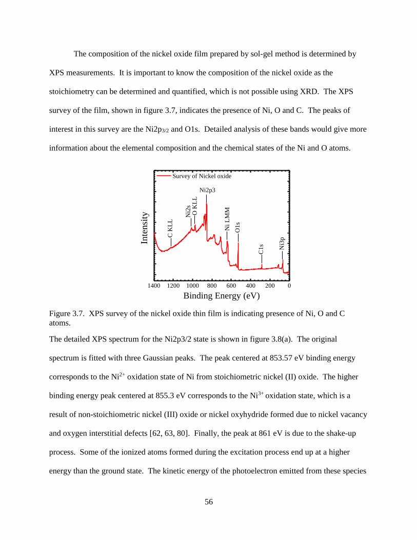
56
The composition of the nickel oxide film prepared by sol-gel method is determined by
XPS measurements. It is important to know the composition of the nickel oxide as the
stoichiometry can be determined and quantified, which is not possible using XRD. The XPS
survey of the film, shown in figure 3.7, indicates the presence of Ni, O and C. The peaks of
interest in this survey are the Ni2p3/2 and O1s. Detailed analysis of these bands would give more
information about the elemental composition and the chemical states of the Ni and O atoms.
Figure 3.7. XPS survey of the nickel oxide thin film is indicating presence of Ni, O and C
atoms.
The detailed XPS spectrum for the Ni2p3/2 state is shown in figure 3.8(a). The original
spectrum is fitted with three Gaussian peaks. The peak centered at 853.57 eV binding energy
corresponds to the Ni2+ oxidation state of Ni from stoichiometric nickel (II) oxide. The higher
binding energy peak centered at 855.3 eV corresponds to the Ni3+ oxidation state, which is a
result of non-stoichiometric nickel (III) oxide or nickel oxyhydride formed due to nickel vacancy
and oxygen interstitial defects [62, 63, 80]. Finally, the peak at 861 eV is due to the shake-up
process. Some of the ionized atoms formed during the excitation process end up at a higher
energy than the ground state. The kinetic energy of the photoelectron emitted from these species
1400 1200 1000 800 600 400 200 0N
i3p
C1
s
O1
s
Ni
LM
M
Ni2p3O
KL
LN
i2s
Inte
nsi
ty
Binding Energy (eV)
Survey of Nickel oxideC
KL
L

57
is decreased and appears as shake-up process at higher binding energy when compared to the
main peak. Figure 3.8(b) shows the XPS spectrum O1s state. The peaks at 529.1 eV and 530.98
eV correspond to nickel (II) oxide and nickel (III) oxide or nickel oxyhydride, respectively [62,
63, 80]. The stoichiometry of the material is determined by comparing the integral area of the
fitted peaks. The atomic ratio of Ni to O in the film is 1:1.70 indicating a Ni deficient film.
Stoichiometric nickel oxide, which exhibits a rock salt structure has a 1:1 atomic ratio. Also, the
ratio of Ni2+ to Ni3+ in the film is 1:2.45. The presence of more Ni3+ indicates that the film is
non-stoichiometric as the formation of Ni3+ oxidation state is due to Ni vacancy.
(a) (b)
Figure 3.8. The composition of the nickel oxide HTL is measured from the integral area of (a)
Ni peaks of Ni2p3/2 and (b) O peaks of O1s curves from the XPS spectrum of nickel oxide.
From the structural and compositional properties investigated using XRD, Raman and
XPS spectroscopies it is clear that the nickel oxide film used in this project non-stoichiomrtic
with defects. The film is further characterized by investigating the optical and electrical
properties.

58
3.1.2.2. Morphological properties
The nickel oxide thin film is polycrystalline with grain size ~13.6 nm. The QLED is
fabricated by layer by layer deposition and hence the interficial properties between adjacent
layers play a significant role in device operation. It is critical that the layers are uniform with
very low roughness to reduce interficial defects and traps. The surface morphology of the nickel
oxide film grown by the optimized process is evaluated using AFM. The 2D ans 3D AFM
images of the sample on glass with a scan area of 1x1 µm2 are shown in figure 3.9 (a). The RMS
and mean roughness are calculated by processin gthe AFM results using the Nanoscope AFM
imag eanalysis software. The average roughness is 1.24 nm and the RMS roughness is 1.7nm as
seen in th results shown in figure. These values are comparable to the roughness of organic
HTLs commonly used with hybrid QLEDs [53]. The thickness of the HTL for QLED
applications should be less than 100 nm as the mobility and conductivity of these materials are
lower compared to other semiconductors. The thickness of the nickel oxide used in this project
is optimized by spin coating the precursor sol-gel at different spin speeds. A 60 – 70nm film is
obtained when the precursor is spin coated at 5000 rpm for 30 s. This is measured using a cross
sectional SEM image as shown in figure 3.9(b).
(a)

59
(b)
Figure 3.9. (a) 2D AFM images of the nickel oxide film are used to determine the surface quality
of the film. The RMS roughness is ~1 nm indicating a very smooth film. (b) Thickness of the
nickel oxide thin film is measured using a cross-sectional SEM image
3.1.2.3. Optical properties
The optical properties of the nickel oxide thin film are investigated by measring the
absorbance and photoluminescence spectra. For absorbance measurement, glass is used as the
baseline. The glass absorbance is measured between 200 – 800nm with an interval of 1nm. A
nickel oxide thin film is grown on the glass using the optimized procedure and the absorbance of
nickel oxide and glass are measrued. The spectrometer program automatically subtracts the glass
baseline absorbance and the final spetrum is purely of nikcel oxide thin film. The baseline and
absorbance of nickel oxide thin film are shown in figure 3.10 (a). The broad visible abrobance
between 470 and 660 nm with a peak centered at 552 nm is from the defect levels within the
band gap of nickel oxide. Band gap of nickel oxide is usually reported between 3.2 to 3.7 eV
[62, 63, 69]. For the non-stoichiometic nickel oxide used in this project the band gap is found to
be as 3.22 eV. This is calculated from the band edge absrobance peak of the absorbance
spectrum centered at 385 nm. This peak can be clearly seen in figure. The photoluminescence
spectrum of the nickel oxide thin film is shown in figure 3.10 (b). The wide spectrum is due to
emission from the defect levels within the nickel oxide band gap. The band edge of the nickel
oxide is not excited as the spectrometer laser is limited in energy to 2.61 eV, while the band gap

60
of nickel oxide as calculated from the absorbance spectrum is 3.22 eV. It can be noted that the
spectrum consists of two prominent peaks at 570 nm and 790 nm that are convoluted together. It
is due to emission from two different bands located within the band gap.
(a) (b)
Figure 3.10. (a) The band gap of the nickel oxide thin film is extracted from the excitonic peak
located at 385 nm of the absorbance spectrum. (b) The defect related photoluminescence
spectrum of the nickel oxide thin film extends from 445 nm to 900 nm. Reprinted with
permission from Vasan et. al. [50].
Since, the defects facilitate the transport of carriers across the QLED, it is important to
characterize the defects by measuring the carrier lifetime using time resolved
photoluminescence. The excitation is achieved by a 485 nm laser and so the band edge is not
excited. Any carrier lifetime measured in this case is for the defect levels of nickel oxide thin
film and not the band edge. Initially the nickel oxide samples were prepared on glass substrates
and lifetime decay curve was measured. The decay curve is fitted with four exponential
functions and this is shown in figure 3.11 (a). The fit is very good with very low residuals. The
average lifetime is calculated as 1.31 ns. The short lifetime is understandable as the defect states
are usually shorlived. In order to check the validity of this value, the same experiemnt was
repeated on quartz substrate and this is shown in figure 3.11 (b). In this case the decay curve is

61
fitted with three exponential functions and the carrier lifetime is calculated as 1.97 ns. Within
experiemntal errors this value is in good agrrement with the nickel oxide film on glass.
(a) (b)
Figure 3.11. Average lifetime of nickel oxide defect states is calculated by fitting the decay
curves measured on (a) glass and (b) quartz.
3.1.2.4. Electrical Properties
The non-stoichiometric nickel oxide grown using similar techniques is a p-type
semiconductor. In order to determine this, a hot probe experiment is used to know the type of
nickel oxide grown in this project. A schematic of the hot probe experiment is shown in figure
3.12. The probes of a voltmeter are made to contact the sample surface and the positive probe is
heated using a soldering iron. The increased temperature generates majority carriers near the
positive probe, which in this case are the holes. The excess holes start to diffuse towards the
cold probe leaving behind negative charges at the hot probe. This separation of charges creates a
voltage, which is read using the voltmeter. The voltage in this case has a negative value.
2 3 4 5 6 7 80.0
0.1
0.2
0.3
0.4
0.5
0.6
0.7
0.8
0.9
1.0
Decay Curve
Fit
Norm
ali
zed
Inte
nsi
ty (
a.u.)
Time (ns)
Nickel oxide thin film on quartz
2 3 4 5 6 7 80.0
0.1
0.2
0.3
0.4
0.5
0.6
0.7
0.8
0.9
1.0
Nickel oxide thin film on glass
Decay curve
Fit
Norm
ali
zed
Inte
nsi
ty (
a.u.)
Time (ns)

62
Figure 3.12. Schematic of the hot probe experiment to deduce the conduction type of nickel
oxide thin film.
The mobility and band positions are extracted from the current-voltage characteristics an
FTO/NiO/Al Schottky diode. From the hot probe experiment it is clear that the non-
stoichiometric nickel oxide is a p-type semiconductor with holes as the majority carrier. The
hole mobility is extracted from the current-voltage characteristics of the Schottky diode at room
temperature. The current-voltage characteristic of the diode in log-log plot is shown in figure
3.13.
Figure 3.13. The log-log plot of the current-voltage characteristics of the nickel oxide Schottky
diode is fitted with linear function to understand the conduction mechanism. Slope of 1 indicates
an Ohmic conduction and a slope of 2 indicates a space charge limited conduction.
0.01 0.1 1
1E-5
1E-4
1E-3
0.01
0.1
JV
log-log IV plot
Linear fit
Curr
ent
Den
sity
(A
/cm
2)
Voltage (V)
JV2

63
The plot is fitted with two linear fits with slopes ~1 and ~2. This is critical as the slopes give
insights into the type of current conduction within the diode. Initially at low electric field, the
current conduction is limited by the intrinsic carrier density and thermally generated carriers.
For this diode the region between 0.1 V and 0.5 V yields a slope of ~1. This conduction regime
is the Ohmic region where JαV1. As the voltage is increased further the diode enters the high
field regime, where the current density follows the square law (JαV2). This conduction regime is
called the space charge limited conduction [81, 82]. In this regime, the current conduction is
dominated by the holes that are injected from the electrode. The current in this case is limited
only the mobility of holes and not dependent on the hole density. Hence, mobility is calculated
by fitting the current-voltage characteristics of the diode using the Mott-Gurney law given by
equation 3.3 that describes the current in this regime [81, 82].
JSCLC = 9
8 ε0εrµh
V2
d3 (3.3)
where, JSCLC is the space charge limited current density, ε0 is the permittivity of free space, εr is
the dielectric constant of nickel oxide, µh is the hole mobility, V is the forward voltage and d is
the thickness of the active layer. The current-voltage characteristics of the diode with the space
charge limited current model fit are shown in figure 3.14. The fit is good with very low chi-
square value. For fitting, the dielectric constant of nickel oxide is taken as 5.7 and the thickness
of active layer as 300 nm. From this curve fitting the hole mobility is found to be, µh = 2.45 ×
10−4 cm2V−1s−1 with an error of ±9.2 × 10⁻⁷ cm2V−1s−1. This method is applicable when the
conduction is unipolar and with an assumption that the mobility, dielectric constant are the same
throughout the material.

64
Figure 3.14. Space charge limited current model is fitted to current-voltage characteristics of a
FTO/NiO/Al device to extract the hole mobility of the nickel oxide thin film. Reprinted with
permission from Vasan et. al. [52].
The valence band and conduction band positions are calculated from the Schottky barrier
height. The Schottky barrier height ϕB is calculated using two different methods for
consistency. Cheung and Cheung came up with a method to calculate the barrier height and
ideality factor which is the one of the methods used in this project [83]. According to this
method the diode current is given by equation 3.4.
I = I0eq(V−IRs)
nkT (3.4)
where, I is the forward current, I0 is the saturation current, V is the forward voltage, T the
temperature, k the Boltzmann constant, n the ideality factor and Rs is the series resistance of the
device. The ideality factor is calculated using a plot of I vs dV/d(ln I) as shown in the equation
3.5.
dV
d(ln I)=
nkT
q+ IRs (3.5)
The linear plot of dV/d(ln I) as a function of I is shown in figure 3.15. From the intercept of this
plot, the ideality factor at room temperature is calculated as 13.6. The high ideality factor
1 2 3 4 51E-4
1E-3
0.01
0.1
1
h= 2.45x10
-4 cm
2V
-1s
-1
IV curve
Fit
Curr
ent
(A/c
m2)
Voltage (V)
Standard Error = 9.209x10⁻⁷ cm
2V
-1s
-1
Reduced Chi-Sqr = 7.88E-6
Adj. R-Square = 0.98539

65
indicates the non-ideal diode characteristics associated with bulk defects in the semiconductor
and interface states between Al and nickel oxide [84, 85]. To calculate the barrier height,
equation 3.6 and 3.7 are used.
H(I) = V −nkT
qln (
I
AA∗T2) (3.6)
H(I) is a parameter calculated from the current-voltage characteristics and the plot of I vs H(I)
yields a linear plot as shown in figure 3.15. Also,
H(I) = nϕB + IRs (3.7)
Hence, from the intercept of the linear fit of I vs H(I) is equal to nϕB. Using n=13.6, the barrier
height is calculated as 0.40 eV.
Figure 3.15. Cheung’s method [83] is employed to extract the barrier height and ideality factor
of the Al/NiO Schottky diode.
In the second method, the current-voltage characteristic of the diode is measured at
different temperatures [86]. To extract the Schottky barrier height using this method, the diode
current-voltage characteristics are measured at 25oC, 50oC, 75oC, and 100oC. The packaged
diode is placed on a hot plate and the measurement is performed at these temperatures. The
current-voltage characteristics of the diode at different temperatures are shown in figure 3.16(a).
0.0 2.0x10⁻⁵
4.0x10⁻⁵
6.0x10⁻⁵
8.0x10⁻⁵
1.0x10⁻⁴
5.0
5.2
5.4
5.6
5.8
6.0
6.2
H (
I) (
V)
Current (A)
-1.0
-0.5
0.0
0.5
1.0
1.5
2.0
2.5
3.0
3.5
4.0
dV
/d(l
n I
)(V
)
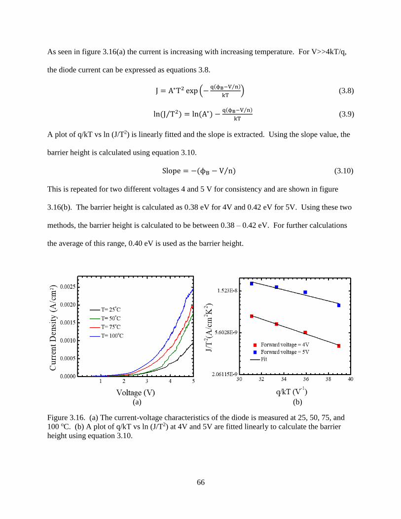
66
As seen in figure 3.16(a) the current is increasing with increasing temperature. For V>>4kT/q,
the diode current can be expressed as equations 3.8.
J = A∗T2 exp (−q(ϕB−V n⁄ )
kT) (3.8)
ln(J T2⁄ ) = ln(A∗) −q(ϕB−V n⁄ )
kT (3.9)
A plot of q/kT vs ln (J/T2) is linearly fitted and the slope is extracted. Using the slope value, the
barrier height is calculated using equation 3.10.
Slope = −(ϕB − V n⁄ ) (3.10)
This is repeated for two different voltages 4 and 5 V for consistency and are shown in figure
3.16(b). The barrier height is calculated as 0.38 eV for 4V and 0.42 eV for 5V. Using these two
methods, the barrier height is calculated to be between 0.38 – 0.42 eV. For further calculations
the average of this range, 0.40 eV is used as the barrier height.
(a) (b)
Figure 3.16. (a) The current-voltage characteristics of the diode is measured at 25, 50, 75, and
100 oC. (b) A plot of q/kT vs ln (J/T2) at 4V and 5V are fitted linearly to calculate the barrier
height using equation 3.10.

67
A schematic of the energy band diagram of Al/NiO Schottky diode is shown in figure
3.17. The band gap of the nickel oxide found using the absorbance spectrum is 3.22 eV and the
work function of Al is 4.30 eV and finally the barrier height as calculated above is 0.40 eV.
Figure 3.17. The energy band diagram of the nickel oxide Schottky diode is used to extract the
CBM and VBM values of nickel oxide thin film.
Using these values, the electron affinity, χ, is calculated using equation
ϕb = Eg + χ − ϕm
0.40 = 3.22 + χ − 4.28
χ = 1.46 eV
The valence band position is then calculated as ~4.70 eV. The bandgap, electron affinity and the
valence band maximum of nickel oxide obtained from the diode characteristics are lower than
the reported results.
3.1.3. Nickel oxide nanoparticles
3.1.3.1. Structural and compositional properties
The structural and compositional properties of the nickel oxide nanoparticles are
characterized by XRD, Raman and XPS measurements. The grazing angle XRD scan of the
nickel oxide nanoparticle powder is shown in figure 3.17 (a). The diffracting planes (111),
(200), (220), (311), and (222) located at 37.2o, 43.27o, 62.8o, 75.3o, and 79.3o respectively, are

68
characteristic of nickel oxide rock salt structure. The reference indices for bunsenite structure
from JCPDS card no: 01-075-0197 are also marked in figure 3.18(a). The crystallite size, as
calculated from Scherrer’s equation, is 5 – 6 nm indicating that the formed nickel oxide is
nanocrystalline. Nickel oxide thin films and nanoparticles reported so far are non-stoichiometric
with nickel vacancies [62, 63, 80, 87]. Presence of these defects are identified by the shift in the
diffraction peaks, specifically the (200) and (220) planes, when compared to stoichiometric
nickel oxide or bunsenite [63]. The nickel oxide nanoparticles reported here are near-
stoichiometric with fewer defects as the diffraction planes exactly align with the bunsenite
reference indices. This can also be seen in the Raman spectrum of the nickel oxide nanoparticles
shown in figure 3.18(b). The LO phonon mode at 510 cm-1 is characteristic of near-
stoichiometric nickel oxide. This mode is shifted to 560 cm-1, when the nickel oxide is formed in
an oxygen rich environment leading to the formation of nickel vacancies, which makes the final
nickel oxide non-stoichiometric [66].
(a) (b)
Figure 3.18. The (a) XRD and (b) Raman spectroscopy are used to structurally characterize the
nickel oxide nanoparticles. Reprinted with permission from Vasan et. al. [70].

69
The composition of the nickel oxide nanoparticles is determined by XPS measurements.
A survey of the material indicates the presence of nickel, oxygen and carbon. The carbon is
from the nickel acetate, which is the precursor. The detailed XPS spectrum for the Ni2p3/2 state
is shown in figure 3.19(a). The original spectrum is fitted with three Gaussian peaks. The peak
centered at 854.2 eV binding energy corresponds to the Ni2+ oxidation state of Ni from
stoichiometric nickel (II) oxide. The higher binding energy peak at 856.0 eV corresponds to the
Ni3+ oxidation state, which is a result of non-stoichiometric nickel (III) oxide or nickel
oxyhydride formed due to nickel vacancies [62, 63]. Finally, the peak at 861 eV is due to the
shake up process [62]. Figure 3.19(b) shows the XPS spectrum O1s state. The peaks at 529.1
eV and 530.98 eV correspond to nickel (II) oxide and nickel (III) oxide or nickel oxyhydride
respectively [62, 63]. The composition ratio of Ni2+ to Ni3+ is 1:1.7 as calculated from the
integral area of the fitted peaks. The amount of Ni3+ formed due to nickel vacancies is much
lower compared to nickel oxide thin film. Moreover, the atomic ratio of Ni:O in the nickel oxide
nanoparticles is 1:1.18 indicating a near-stoichiometric nickel oxide.
(a) (b)
Figure 3.19. The composition of the nickel oxide HTL is measured from the (a) Ni peaks of
Ni2p3/2 and (b) O peaks of O1s curves from the XPS. Reprinted with permission from Vasan et.
al. [50].

70
From the structural and compositional properties investigated using XRD, Raman and
XPS spectroscopies it is clear that the nickel oxide film used in this project non-stoichiomrtic
with defects. The film is further characterized by investigating the optical properties.
3.1.3.2. Optical properties
The optical properties of nickel oxide nanoparticles and the quantum dots are investigated
by measuring the absorbance. The absorbance of nickel oxide nanoparticles is shown in figure
3.20. The band gap of the synthesized near-stoichiometric nickel oxide nanoparticles as
calculated from the excitonic peak at 280 nm is 4.42 eV. This band gap value is much higher
than the band gap of non-stoichiometric nickel oxide thin film, which is around 3.22 eV. The
photoluminescence measurements revealed no emission in the visible region as was seen with
the nickel oxide thin film.
Figure 3.20. The band gap of the nickel oxide nanoparticles is calculated from the excitonic
peak of the absorbance spectrum. Reprinted with permission from Vasan et. al. [70].
200 300 400 500 600 700 8000.0
0.2
0.4
0.6
0.8
1.0
1.2
Ab
sorb
ance
(a.
u.)
Wavelength (nm)
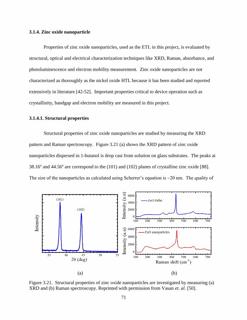
71
3.1.4. Zinc oxide nanoparticle
Properties of zinc oxide nanoparticles, used as the ETL in this project, is evaluated by
structural, optical and electrical characterization techniques like XRD, Raman, absorbance, and
photoluminescence and electron mobility measurement. Zinc oxide nanoparticles are not
characterized as thoroughly as the nickel oxide HTL because it has been studied and reported
extensively in literature [42-52]. Important properties critical to device operation such as
crystallinity, bandgap and electron mobility are measured in this project.
3.1.4.1. Structural properties
Structural properties of zinc oxide nanoparticles are studied by measuring the XRD
pattern and Raman spectroscopy. Figure 3.21 (a) shows the XRD pattern of zinc oxide
nanoparticles dispersed in 1-butanol is drop cast from solution on glass substrates. The peaks at
38.16o and 44.56o are correspond to the (101) and (102) planes of crystalline zinc oxide [88].
The size of the nanoparticles as calculated using Scherrer’s equation is ~20 nm. The quality of
(a) (b)
Figure 3.21. Structural properties of zinc oxide nanoparticles are investigated by measuring (a)
XRD and (b) Raman spectroscopy. Reprinted with permission from Vasan et. al. [50].

72
the zinc oxide nanoparticles is also evaluated using Raman spectroscopy. Raman spectrum of
zinc oxide nanoparticles compared with the spectrum of commercially available zinc oxide
pellets (Kurt. J Lesker) are shown in figure 3.21(b). The peaks at 334 cm-1, 441 cm-1, and 582
cm-1 are characteristic of zinc oxide.
3.1.4.2. Optical properties
Optical properties of zinc oxide nanoparticles are studied using absorbance and
photoluminescence spectroscopies. The bandgap zinc oxide is calculated from the excitonic
peak shown in figure. The peak is at 334 nm, which corresponds to 3.71 eV. The normalized
photoluminescence spectrum of the zinc oxide nanoparticle is shown in figure 3.22. The small
peak at 355 nm corresponds to the excitation laser and the peak at 365 nm corresponds to the
band edge emission of zinc oxide nanoparticles. The FWHM of the spectrum is 32 nm
indicating that the nanoparticle sizes are uniformly distributed.
Figure 3.22. The absorbance and photoluminescence spectra of the zinc oxide ETL that was
synthesized by hydrolysis of Zinc precursor using ammonium hydroxide. Reprinted with
permission from Vasan et. al. [50].
300 350 400 450 500 550 6000.0
0.2
0.4
0.6
0.8
1.0
Wavelength (nm)
No
mal
ized
In
ten
sity
(a.
u.)
1.0
1.5
2.0
2.5
3.0
3.5
4.0
4.5A
bso
rban
ce (
a. u
.)

73
3.1.4.3. Electrical properties
Zinc oxide nanoparticles are intrinsically n-type due to inherent defects. Mobility is one
of the electrical parameters that changes with the synthesis procedure and hence it should be
measured. In this project, the mobility is measured by fabricating a thin film transistor with the
nanoparticles in the channel. The gate-source voltage, VGS is swept from 0-20 V with constant
drain-source voltage, VDS and corresponding drain-source current, IDS is measured. The VGS vs
IDS for different VDS are plotted in figures 3.23(a). As seen in figure 3.23(a), the threshold
voltage is ~4V and with increasing VDS, the drain current increases. For VDS > (VGS-VT) the
device enters saturation regime in which the drain current is no longer a function of VDS. In the
saturation region, the mobility of the channel material is calculated from the slope of the transfer
characteristics, VGS vs (IDS)1/2. From the slope of VGS vs (IDS)1/2 shown in figure 3.23(b), the
electron mobility is calculated as 1.24×10⁻² cm2V-1s-1.
(a) (b)
Figure 3.23. (a) The gate-source voltage of the thin film transistor is swept, and corresponding
drain current is measured for different drain-source voltages. (b) A plot of VGS vs (IDS)1/2 in the
saturation region of the thin film transistor yields a linear curve. This is linearly fitted to extract
the electron mobility of zinc oxide nanoparticles. Reprinted with permission from Vasan et. al.
[52].

74
3.2. Charge transport model
To make an efficient QLED, it is important to improve the charge transport efficiency
into the quantum dot emissive layer. Zinc oxide nanoparticles commonly used for electron
transport has a CBM aligned very well the CB of the quantum dots. It is widely accepted that the
zinc oxide nanoparticles facilitate efficient electron transport by direct charge injection
mechanism [42-52]. So, the transport efficiency is limited by the hole transport to the emissive
layer. The nickel oxide thin film and nanoparticles in this project are designed such that they
facilitate hole transport by resonant energy transfer and direct charge injection mechanism,
respectively. In this section the charge transport between HTLs and quantum dot emissive layer
is evaluated and modelled.
3.2.1. Resonant energy transfer in nickel oxide thin film-quantum dot bilayer
The charge transport between non-stoichiometric nickel oxide thin film and quanutm dot
emissive layer is investigated on a nickel oxide-quanutm dot bilayer. Time resolved
photoluminescence, photoluminescence, and absorbance measurements are used to study the
carrier dynamics in the bilayer samples. For energy transfer to occur from nickel oxide HTL to
quanutm dot layer, energitically resonant states are required and the layers need to be in close
contact. The layers are in close proximity as the quanutm dots are spin coated directly onto the
nickel oxide HTL. The bandgap of nickel oxide is 3.22 eV, which is well over the bandgaps of
visible light emitting quanutm dots. So any form of resonant energy transfer between the band
edge states are ruled out. As established from the structural, optical and electrical properties, the
nickel oxide thin film is non-stoichiometric with nickel vacnacies. These vacnacies lead to the
formation of defect states within the bandgap of nickel oxide. These defect states are involved in
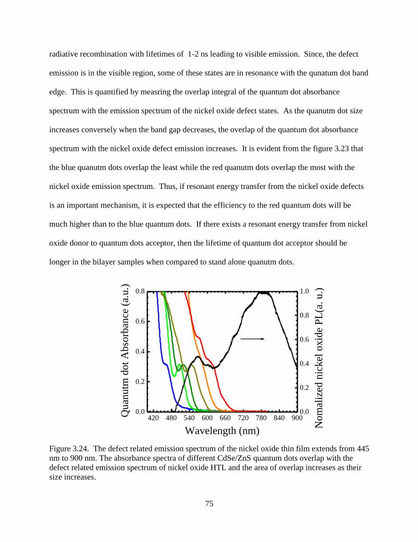
75
radiative recombination with lifetimes of 1-2 ns leading to visible emission. Since, the defect
emission is in the visible region, some of these states are in resonance with the qunatum dot band
edge. This is quantified by measring the overlap integral of the quantum dot absorbance
spectrum with the emission spectrum of the nickel oxide defect states. As the quanutm dot size
increases conversely when the band gap decreases, the overlap of the quantum dot absorbance
spectrum with the nickel oxide defect emission increases. It is evident from the figure 3.23 that
the blue quanutm dots overlap the least while the red quanutm dots overlap the most with the
nickel oxide emission spectrum. Thus, if resonant energy transfer from the nickel oxide defects
is an important mechanism, it is expected that the efficiency to the red quantum dots will be
much higher than to the blue quantum dots. If there exists a resonant energy transfer from nickel
oxide donor to quantum dots acceptor, then the lifetime of quantum dot acceptor should be
longer in the bilayer samples when compared to stand alone quanutm dots.
Figure 3.24. The defect related emission spectrum of the nickel oxide thin film extends from 445
nm to 900 nm. The absorbance spectra of different CdSe/ZnS quantum dots overlap with the
defect related emission spectrum of nickel oxide HTL and the area of overlap increases as their
size increases.
420 480 540 600 660 720 780 840 9000.0
0.2
0.4
0.6
0.8
Quan
utm
dot
Abso
rban
ce (
a.u.)
Wavelength (nm)
0.0
0.2
0.4
0.6
0.8
1.0
Nom
aliz
ed n
ickel
oxid
e P
L(a
. u.)

76
The fluorescence lifetimes of six different quantum dot sizes in the form of films are
measured both on bare glass and nickel oxide films. The fluorescence decay curves of quantum
dots on glass and on nickel oxide are plotted in figure 3.25(a) to (f). It is clear from these plots
that the lifetime of quantum dots changes on nickel oxide HTL. The change shows a pattern
where the lifetime quenches on blue quantum dots and elongates on cyan, green, yellow, orange
and red quantum dots. Moreover, the elongation increases as the size of the quantum dots
(a) (b)
(c) (d)
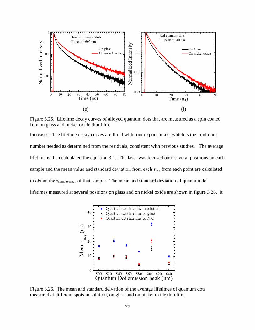
77
(e) (f)
Figure 3.25. Lifetime decay curves of alloyed quantum dots that are measured as a spin coated
film on glass and nickel oxide thin film.
increases. The lifetime decay curves are fitted with four exponentials, which is the minimum
number needed as determined from the residuals, consistent with previous studies. The average
lifetime is then calculated the equation 3.1. The laser was focused onto several positions on each
sample and the mean value and standard deviation from each τavg from each point are calculated
to obtain the τsample-mean of that sample. The mean and standard deviation of quantum dot
lifetimes measured at several positions on glass and on nickel oxide are shown in figure 3.26. It
Figure 3.26. The mean and standard deivation of the average lifetimes of quantum dots
measured at different spots in solution, on glass and on nickel oxide thin film.

78
can be noted that the lifetime of the respective quantum dots in solution is much higher than that
of the film on both bare glass and on the nickel oxide film. It is known that quantum dot lifetime
is quenched when formed in to a film due to self-quenching effects [53]. In order to explore this
further the percentage of lifetime qurenching on glass and nickel oxide are calculated for all
quanutm dots. Figure 3.27 shows the percentage lifetime quenching on bare glass and nickel
oxide relative to those in solution as a function of quanutm dot size. It can be noted that the
lifetime of quanutm dots quenches by approximately 52% on bare glass regardless of the size of
the quanutm dot. On the other hand, the lifetime quenching of quanutm dots on nickel oxide
shows strong size dependence. The percent quenching decreases as the size of the quanutm dots
increases. While the lifetime of blue-emitting quantum dots on nickel oxide quench by ~52%,
similar to that on bare glass, the lifetime of red-emitting quantum dots quench by only ~36% on
nickel oxide. This shows that there is a strong interaction between the nickel oxide and the
quantum dots and that this interaction is dependent on the bandgap of the quanutm dot. To
Figure 3.27. The percentage quenching of quantum dot lifetime on nickel oxide and glass are
plotted as a function of emission wavelength. In this the lifetime of quantum dots in hexane is
considered as the control sample or reference.
500 520 540 560 580 600 620 6400
10
20
30
40
50
60
70
80
90
100
Per
centa
ge
quen
chin
g (
%)
Quantum dot emission peak (nm)
Lifetime quenching on glass
Lifetime quenching on nickel oxide
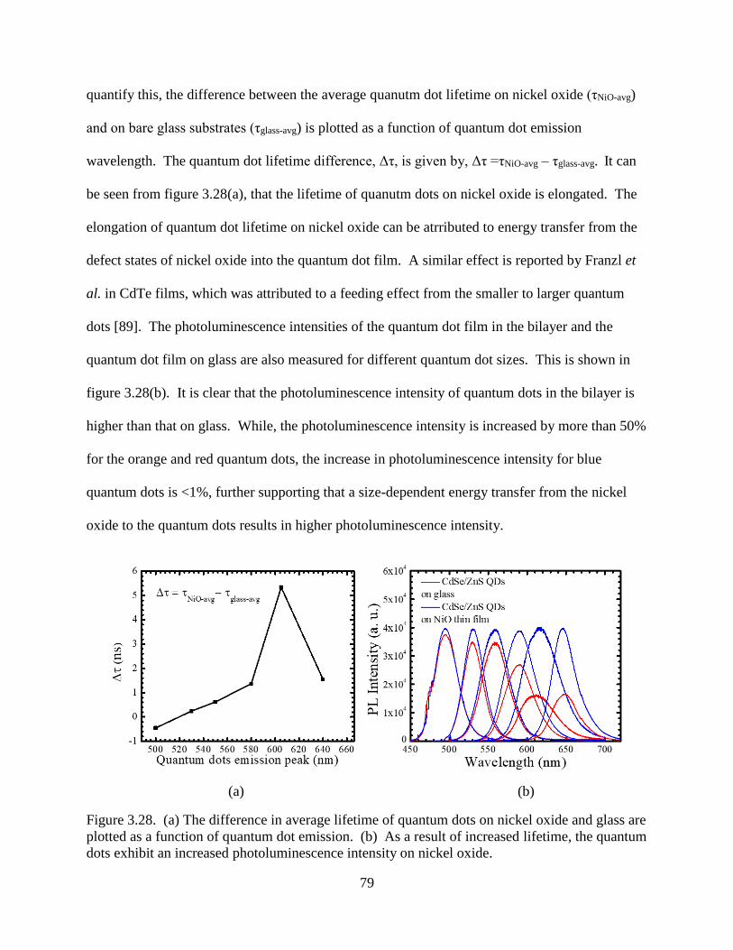
79
quantify this, the difference between the average quanutm dot lifetime on nickel oxide (τNiO-avg)
and on bare glass substrates (τglass-avg) is plotted as a function of quantum dot emission
wavelength. The quantum dot lifetime difference, Δτ, is given by, Δτ =τNiO-avg – τglass-avg. It can
be seen from figure 3.28(a), that the lifetime of quanutm dots on nickel oxide is elongated. The
elongation of quantum dot lifetime on nickel oxide can be atrributed to energy transfer from the
defect states of nickel oxide into the quantum dot film. A similar effect is reported by Franzl et
al. in CdTe films, which was attributed to a feeding effect from the smaller to larger quantum
dots [89]. The photoluminescence intensities of the quantum dot film in the bilayer and the
quantum dot film on glass are also measured for different quantum dot sizes. This is shown in
figure 3.28(b). It is clear that the photoluminescence intensity of quantum dots in the bilayer is
higher than that on glass. While, the photoluminescence intensity is increased by more than 50%
for the orange and red quantum dots, the increase in photoluminescence intensity for blue
quantum dots is <1%, further supporting that a size-dependent energy transfer from the nickel
oxide to the quantum dots results in higher photoluminescence intensity.
(a) (b)
Figure 3.28. (a) The difference in average lifetime of quantum dots on nickel oxide and glass are
plotted as a function of quantum dot emission. (b) As a result of increased lifetime, the quantum
dots exhibit an increased photoluminescence intensity on nickel oxide.
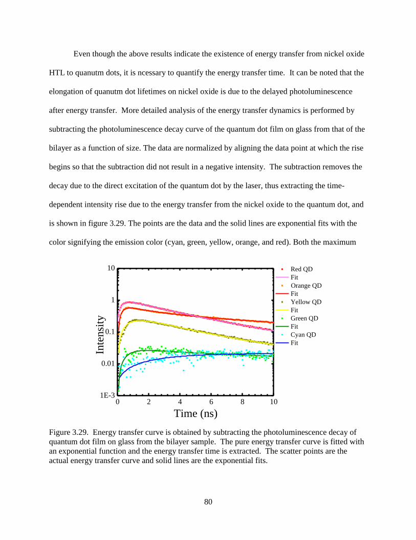
80
Even though the above results indicate the existence of energy transfer from nickel oxide
HTL to quanutm dots, it is ncessary to quantify the energy transfer time. It can be noted that the
elongation of quanutm dot lifetimes on nickel oxide is due to the delayed photoluminescence
after energy transfer. More detailed analysis of the energy transfer dynamics is performed by
subtracting the photoluminescence decay curve of the quantum dot film on glass from that of the
bilayer as a function of size. The data are normalized by aligning the data point at which the rise
begins so that the subtraction did not result in a negative intensity. The subtraction removes the
decay due to the direct excitation of the quantum dot by the laser, thus extracting the time-
dependent intensity rise due to the energy transfer from the nickel oxide to the quantum dot, and
is shown in figure 3.29. The points are the data and the solid lines are exponential fits with the
color signifying the emission color (cyan, green, yellow, orange, and red). Both the maximum
Figure 3.29. Energy transfer curve is obtained by subtracting the photoluminescence decay of
quantum dot film on glass from the bilayer sample. The pure energy transfer curve is fitted with
an exponential function and the energy transfer time is extracted. The scatter points are the
actual energy transfer curve and solid lines are the exponential fits.
0 2 4 6 8 101E-3
0.01
0.1
1
10 Red QD
Fit
Orange QD
Fit
Yellow QD
Fit
Green QD
Fit
Cyan QD
Fit
Inte
nsi
ty
Time (ns)
81
intensity and the transfer rate increased as a function of size, and thus spectral overlap integral.
There is a negligible energy transfer for the blue quantum dots, the cyan quantum dots have a
rise time of approximately 2.9 ns, the green quantum dots have 0.93 ns, the yellow quantum dots
have a 0.75 ns rise time, the orange quantum dots have a 0.26 ns rise time, and the red quantum
dots have a 0.28 ns rise time. With comparable energy transfer time, the tranfer rate to orange
and red quantum dots are comparable ~3.6x10⁹ s-1. Previous studies on multilayer quantum dot
films have shown similar or faster energy transfer times [90-92].
Previous transport models involving all-inorganic bilayers have been based on the
relative energy alignment of the nickel oxide HTL and the valence band of the quantum dot. In
this project, an alternate transport model is proposed based on the structural and spectroscopic
properties of the nickel oxide layer and the quantum dot size. The nickel oxide film is designed
in this project to be highly non-stoichiometric in order to provide enough defect states that are in
resonance with the quantum dot band gap. The defect states within the band gap of the nickel
oxide are in resonance with the band gap of the larger quantum dots, but not so for smaller
quantum dots. Figure 3.28(a) shows that there is an overall increase in the lifetime with quantum
dot size following energy transfer from nickel oxide relative to direct excitation of the quantum
dots alone (i.e. without energy transfer from nickel oxide), as expected from the increased energy
transfer efficiency. However, the increase in quantum dot lifetime (up to 5.5 ns for the orange
quantum dots) is more than an order of magnitude longer than the energy transfer time. This
suggests that quantum dot states that are populated from energy transfer from nickel oxide to the
quantum dot are longer lived, on average, than those populated via direct excitation of the
quantum dot. Figure 3.10(a) shows that there are two broad emission bands from nickel oxide,
one centered around 570nm and the other centered around 790 nm. There are likely a number of

82
trap states in the shell and/or at the core/shell interface that are slightly below the band edge
states and could play a role in the energy transfer and decay dynamics. Direct excitation of the
quantum dots is accomplished by a 485 nm laser, which excites the quantum dots above the band
gap energy – especially the orange and red quantum dots. Due to the absolute energies of the
nickel oxide and quantum dot valence band edges, there is a negligible possibility of direct hole
injection, and thus energy transfer from nickel oxide defect states to quantum dots dominates.
The fact that the broad 570 nm band from the defect nickel oxide states is so close to the band
gap for the orange quantum dots could suggest that some of the trap states in the quantum dots
are directly populated through the energy transfer process, especially from the red edge of the
570 nm band. Trap states generally show longer lifetimes than band edge states [73] and is one
possible explanation of why the fluorescence lifetime of the quantum dot/ nickel oxide bilayer
structures show up to 5.5 ns longer fluorescence decay lifetimes than the quantum dot
monolayers, even though the energy transfer time is sub-ns
A photoluminescence intensity decay is commonly encountered in bilayers where the
valence band of the transport layer aligns with the valence band of the quantum dots that
facilitates efficient charge injection [70]. For example, Wang et al reported a decreased
photoluminescence intensity of perovskite material on a HTL and attributed it to the efficient
charge transport between the two layers by charge injection mechanism [87]. On the other hand,
an increase in the photoluminescence intensity is commonly associated with energy transfer
mechanism [93]. The increase in the steady-state photoluminescence intensity of the quantum
dots in the bilayer (figure 3.28(b)) and that observed by removing the direct quantum dot
excitation contribution in the time-resolved photoluminescence intensity (figure 3.29) are thus in
agreement with this proposed energy transfer mechanism.

83
3.2.2. Charge injection
The charge transport between the near-stoichiometric nickel oxide nanoparticle HTL and
the quantum dots is investigated by time-resolved photoluminescence measurements. The
lifetime of blue, cyan and orange quantum dots are measured in hexane and in solution mixed
with equal amount of nickel oxide nanoparticles. The average lifetimes of blue, cyan and orange
quantum dots in hexane are 17.01 ns, 20.82 ns and 31.67 ns, respectively. These are obtained by
fitting the results shown in figure 3.30 with three exponential decay functions and average
lifetimes are calculated using equation 3.1. It can be noted that the lifetimes of quantum dots
when mixed with nickel oxide nanoparticles are quenched significantly and that the quenching is
dependent on the size of the quantum dot. The lifetime of blue quantum dots quench the highest,
followed by cyan and orange quantum dots. Normally, quantum dot lifetime quenching is
encountered in quantum dot films due to self-quenching effects. In this case, the quantum dots
are still well dispersed in hexane and the lifetime quenching can be attributed to efficient hole
transport from the quantum dots into the nickel oxide nanoparticles.
(a) (b)

84
(c)
Figure 3.30. The lifetime of (a) blue, (b) cyan and (c) orange CdSe/ZnS quantum dots shortened
when mixed with the nickel oxide nanoparticles, which indicates an efficient charge transport
between the two materials. Reprinted with permission from Vasan et. al. [70].
The study shows that the quantum dots exhibit a strong interaction with the nickel oxide
nanoparticle powder. The nickel oxide nanoparticles reported here are near-stoichiometric with
a wide band gap of ~4.4 eV and a deep valence band maximum at -6.22 eV. The valence band
value is calculated from the reported electron affinity value for nickel oxide. It can be seen that
the lifetime of quantum dots is quenched significantly when mixed with the nickel oxide
nanoparticles. Also, lifetime quenching increases with an increase in the band gap of the
quantum dots. In other words, quenching is dependent on the relative valence band alignment of
the quantum dots with nickel oxide nanoparticles. The valence band of blue quantum dots aligns
well with the nickel oxide nanoparticles, leading to 41% quenching in lifetime. The cyan and
orange quantum dots exhibit lower quenching because of the high barrier to holes in these
quantum dots. This is schematically represented in figure 3.31. In contrast, Zheng et.al reported
lifetime quenching decrease with an increase in the bandgap of the quantum dot [12]. The
opposite trend reported here could be due to the deeper valence band maximum of the nickel
oxide nanoparticles, at -6.22 eV, as compared to -5.04 eV reported by Zheng et. al [94]. In a

85
QLED device the barrier to holes injected into the blue quantum dots is much lower when the
nickel oxide nanoparticles are used as HTL. It is clear from figure 3.31 that for other smaller
band gap quantum dots, the barrier to hole injections into the quantum dots is even lower or non-
existent. So far, the reported inorganic HTLs for QLED devices provide a very high barrier to
quantum dots, thus reducing the efficiency. On the other hand, nickel oxide nanoparticles with a
deeper valence band maximum are a potential HTL that can inject holes into the quantum dots of
different sizes more efficiently.
Figure 3.31. Schematic of the charge transport between blue, cyan, and orange quantum dots
and the nickel oxide nanoparticle HTL. Reprinted with permission from Vasan et. al. [70].
3.3. QLED device results
3.3.1. All-inorganic QLED with nickel oxide thin film HTL
3.3.1.1. Green emitting QLED
The performance of QLED is evaluated by measuring the current-voltage characteristics
and light output characteristics. The band alignment of different device layers is shown in figure
3.32. The valence and conduction band positions of zinc oxide and quantum dot emissive layers
are taken from literature [52]. The work function of FTO anode is reported to be 4.6-4.8 eV and
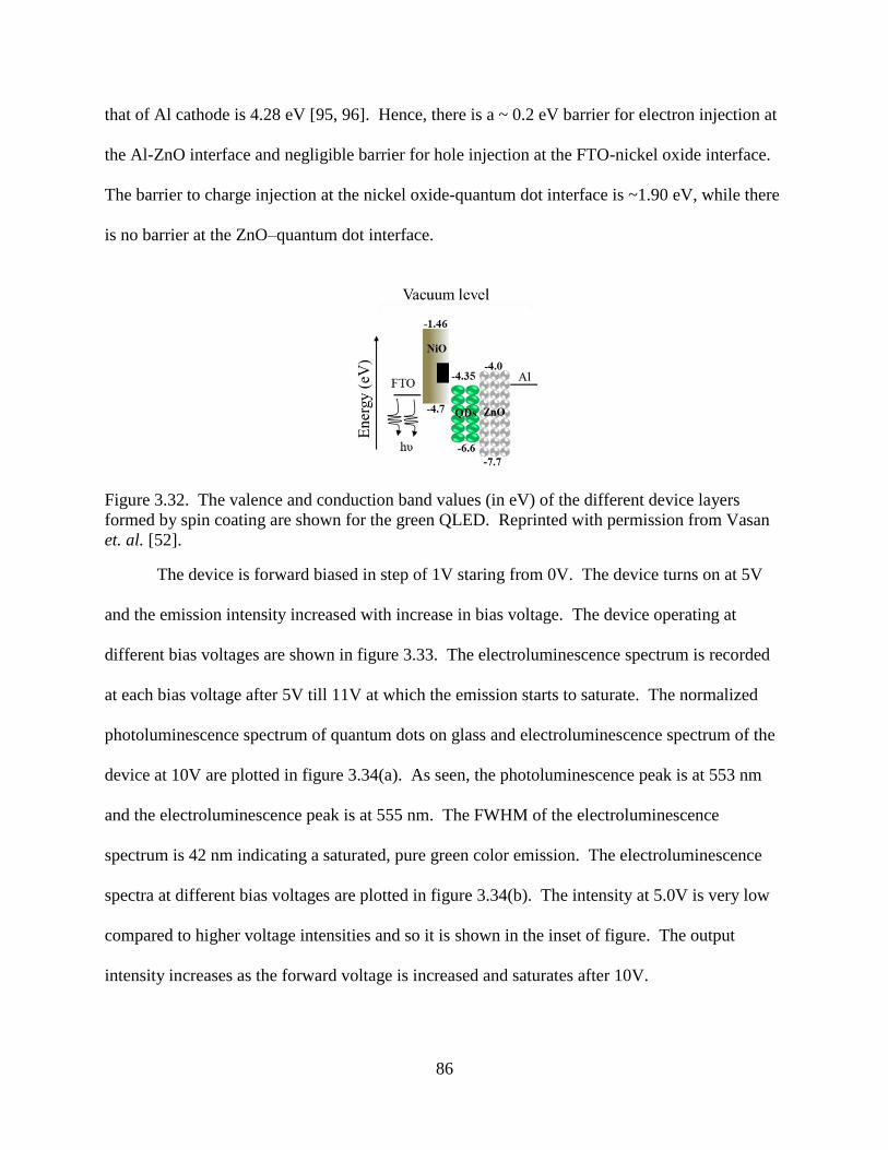
86
that of Al cathode is 4.28 eV [95, 96]. Hence, there is a ~ 0.2 eV barrier for electron injection at
the Al-ZnO interface and negligible barrier for hole injection at the FTO-nickel oxide interface.
The barrier to charge injection at the nickel oxide-quantum dot interface is ~1.90 eV, while there
is no barrier at the ZnO–quantum dot interface.
Figure 3.32. The valence and conduction band values (in eV) of the different device layers
formed by spin coating are shown for the green QLED. Reprinted with permission from Vasan
et. al. [52].
The device is forward biased in step of 1V staring from 0V. The device turns on at 5V
and the emission intensity increased with increase in bias voltage. The device operating at
different bias voltages are shown in figure 3.33. The electroluminescence spectrum is recorded
at each bias voltage after 5V till 11V at which the emission starts to saturate. The normalized
photoluminescence spectrum of quantum dots on glass and electroluminescence spectrum of the
device at 10V are plotted in figure 3.34(a). As seen, the photoluminescence peak is at 553 nm
and the electroluminescence peak is at 555 nm. The FWHM of the electroluminescence
spectrum is 42 nm indicating a saturated, pure green color emission. The electroluminescence
spectra at different bias voltages are plotted in figure 3.34(b). The intensity at 5.0V is very low
compared to higher voltage intensities and so it is shown in the inset of figure. The output
intensity increases as the forward voltage is increased and saturates after 10V.

87
Figure 3.33. Electroluminescence of the green QLED operating at different bias voltages are
shown.
(a) (b)
Figure 3.34. The photoluminescence spectrum of the green quantum dots is compared to that of
the green QLED electroluminescence spectrum(b) Highly saturated, pure color
electroluminescence of the device at different bias voltages. Reprinted with permission from
Vasan et. al. [52].
The IV characteristics of the device are shown in figure 3.35. In order to understand the
working of the device, the IV curve is plotted in log-log scale in which the plot exhibits different
slopes depending on the type of current conduction mechanism. The IV curve exhibits three
distinct slopes, corresponding to Ohmic, trap limited and space charge limited conduction

88
regions [36, 81]. In region I from 0.0 to 4.65V, the slope is 1.2 and hence JαV1.2, which is very
close to an Ohmic behavior. Ohmic current is due to the mobile carriers in the device more
specifically electrons in conduction band or holes in the valence band and is directly proportional
to the applied voltage. The current density increases with a much steeper slope of 4.0 in region
II between 4.65 and 6.25V, which corresponds to trap limited conduction. In this region, the
injected carriers are trapped at the traps on the emissive layer and the interface traps in the CTLs.
At 4.65V the slope changes and this is considered as the onset of charge injection into the
quantum dots [36]. But the turn-on voltage is considered as 5V at which the emission is high
enough to be detected. Finally, the slope of region III between 6.25 and 11V is 2.0, which is the
space charge limited conduction. In this region, the traps are completely filled, and the current is
limited by the space charge created in the device. Trap filled space charge limited current is
usually expressed using Mott-Gurney law given by equation 3.3. Here the current density and
forward voltage have a quadratic relationship and the conduction is dependent on the mobility.
Figure 3.35. The three current conduction regions of the device correspond to the different
slopes in the current-voltage characteristics. Reprinted with permission from Vasan et. al. [52].
1 2 3 4 5 6 7 8 9101
10
100
Curr
ent
Den
sity
(m
A/c
m2)
Voltage (V)
JV4.0
JV1.2
JV2.0

89
The light output characteristics of the device are shown in figure 3.36, which are
calculated assuming a Lambertian emission [97, 98]. In figure 3.36(a), the luminance of the
device is plotted as a function of bias voltage. The voltage at which the device luminance
reaches 1000 cd/m2 is 5.4 V and corresponding current density is 21 mA/cm2. Another 20
mA/cm2 increase in current density increased the luminance to 10,000 cd/m2 at 6.9 V. The
current and external quantum efficiencies of the device, plotted as a function of current density,
are shown in figure 3.36(b). The current efficiency increases initially, reaches a maximum at
10V, and starts to decrease after. The maximum current efficiency of 144 cd/A is obtained at 80
mA/cm2 current density. The EQE shows a similar profile as previously reported for hybrid
QLED and perovskite based solution processed LEDs [9, 19]. The EQE reaches a maximum of
11.4% at 80 mA/cm2 and decreases with further increase in the current density. The luminous
efficiency of the device reaches a peak of 45.3 lm/W and starts to decrease with further increase
in current density. The efficiency roll-off or droop after reaching a peak is due to charging of
quantum dots. At high current densities the quantum dots are charged due to influx of carriers.
These charged quantum dots are rendered non-emissive faster than the radiative recombination
rate as a result of Auger recombination, which leads to efficiency roll-off [36, 53, 99]. Auger
recombination rate is on the order of few ps, while the average radiative lifetime of green
quantum dots is ~19 ns.

90
(a) (b)
Figure 3.36. (a) Luminance of the device is plotted as a function of the bias voltage. The
luminance increases with voltage and saturates at 10V. (b) The current efficiency and EQE are
plotted as a function of current density. Reprinted with permission from Vasan et. al. [52].
3.3.1.2. Yellow emitting QLED
Yellow emitting QLEDs are fabricated using the 570 nm emitting CdSe/ZnS quantum
dots. The band alignment of different device layers is shown in figure 3.37. The band positions
of the CTLs and the work functions of electrodes are the same as shown in figure 3.32. The
band positions of the yellow emitting quantum dots are different than the green quantum dots.
The barrier to charge injection at the nickel oxide-quantum dot interface is ~1.83 eV, while there
is no barrier at the ZnO–quantum dot interface.
Figure 3.37. The valence and conduction band values (in eV) of the different device layers
formed by spin coating are shown for the yellow QLED.

91
The device is forward biased in step of 1V staring from 0V. The device turns on at 5V
and the emission intensity increased with increase in bias voltage. The device operating at 10V
bias voltage is shown in figure 3.38(a). The normalized photoluminescence spectrum of
quantum dots on glass and electroluminescence spectrum of the device at 10V are plotted in
figure 3.38(b). As seen, the photoluminescence peak is at 570 nm and the electroluminescence
peak is at 588 nm. The FWHM of the electroluminescence spectrum is 38 nm indicating a
saturated, sodium yellow color emission. The electroluminescence spectra at different bias
voltages are plotted in figure 3.38(c). The intensity at 5.0V is very low compared to higher
voltage intensities and so it is shown in the inset of figure. The output intensity increases as the
forward voltage is increased and saturates after 8V.
(a)
(b) (c)
Figure 3.38 (a) Yellow QLED operating at 10V. (b) The photoluminescence spectrum of the
yellow quantum dots is compared to that of the yellow QLED electroluminescence spectrum. (c)
Highly saturated, pure color electroluminescence of the device at different bias voltages.

92
The current-voltage characteristic of the device is shown in figure 3.39. Conduction
mechanism of the device is understood by plotting the current-voltage characteristics in log-log
scale. The current-voltage curve exhibits three distinct slopes, corresponding to Ohmic, trap
limited and space charge limited conduction regions [36, 81]. Similar to the green QLED, the
device initially operates in the Ohmic region. The slope changes to 5.4 (JαV5.4) at 4.5 V, which
corresponds to the onset of charge injection. The emission is high enough to be detected only at
5V. In the third region the current increases more gradually with a flatter slope of 3.5. This
again is considered as trap limited conduction. Finally, the relationship between J and V
becomes quadratic at 8.0 V with the onset of space charge limited conduction. In this region, the
traps are completely filled, and the current is limited by the space charge created in the device. It
can be seen that the yellow QLED device operates in the trap limited region between 4.5V and
8.0V. This range is lower for the green emitting QLED. It is reported that QLED emit
efficiently in the trap limited region as the quantum dots are considered as the traps [37].
Figure 3.39. Current-voltage characteristic of the yellow QLED with different current
conduction regions is shown.

93
The light output characteristics of the device are shown in figure 3.40. In figure 3.40(a),
the luminance of the device is plotted as a function of bias voltage. The luminance increases
with voltage and reaches 10,000 cd/m2 at 7.7 V. The voltage at which the device luminance
reaches 1000 cd/m2 is 5.6 V and corresponding current density is 211 mA/cm2 and at 711
mA/cm2 it reaches 10,000 cd/A. The current and external quantum efficiencies of the device,
plotted as a function of current density, are shown in figure 3.40(b). The current efficiency
increases initially, reaches a maximum at 8V, and saturates. The maximum current efficiency of
1.6 cd/A is obtained at 1533.3 mA/cm2 current density. The EQE increases to 1.4% at 900
mA/cm2 and increases to just over 1.5% at 1533.33 mA/cm2. Similar to current and quantum
efficiencies, the luminous efficiency reaches 0.54 lm/W and decreases. As compared to the
green QLED, all performance parameters are much lower. This is mainly due to the carrier
lifetime difference between the quantum dots. The average lifetime of yellow quantum dots in a
packed film is 3.42 ns while that of green quantum dots is 9.0 ns, which indicates that the
quantum yield of yellow quantum dots is much lower than that of the green quantum dots. The
EQE of the QLED is directly proportional to the quantum yield of the quantum dots according to
equation. Hence, to generate the same amount of brightness, the yellow QLED requires higher
current densities. As the current density increases, the number of phonons generated due to non-
radiative recombination increases, which are released into the lattice in the form of thermal
energy. As the temperature of the quantum dots increases it degrades and leads to further
decrease in luminance.

94
(a) (b)
Figure 3.40. (a) Luminance of the yellow QLED is plotted as a function of the bias voltage. The
luminance increases with voltage and saturates at 8V. (b) The current efficiency and EQE of the
device are plotted as a function of current density.
3.3.1.3. Red emitting QLED
Red emitting QLEDs are fabricated using the red (640 nm) emitting CdSe/ZnS quantum
dots. The band alignment of different device layers is shown in figure 3.41. The band positions
of the CTLs and the work functions of electrodes are the same as shown in figure 3.32. The
band positions of the red emitting quantum dots are different than the other quantum dots. The
barrier to charge injection at the nickel oxide-quantum dot interface in this case is ~1.73 eV,
while there is no barrier at the ZnO–quantum dot interface.
Figure 3.41. The valence and conduction band values (in eV) of the different device layers
formed by spin coating are shown for the red QLED.

95
The device is forward biased in step of 1V staring from 0V. The device turns on at 4V
and the emission intensity increased with increase in bias voltage. The device operating at 4V
and 10V bias voltages are shown in figure 3.42(a). The normalized photoluminescence spectrum
of quantum dots on glass and electroluminescence spectrum of the device at 10V are plotted in
figure 3.42(b). As seen, the photoluminescence peak is at 640 nm and the electroluminescence
peak is at 645 nm. The FWHM of the electroluminescence spectrum is 32 nm indicating a
saturated, pure red color emission. The electroluminescence spectra at different bias voltages are
plotted in figure 3.42(c). The intensity at 4.0V is very low compared to higher voltage intensities
and so it is shown in the inset of figure 3.42(c).
(a)
(b) (c)
Figure 3.42. (a) Red QLED operating at 4V and 10V. (b) The photoluminescence spectrum of
the red quantum dots is compared to that of the red QLED electroluminescence spectrum. (c)
Highly saturated, pure red color electroluminescence of the device at different bias voltages.

96
The current-voltage characteristic of the device is shown in figure 3.43. It is plotted in
log-log scale and different linear regions are fitted. The initial Ohmic region ends at 0.45V and
the slope changes to 2.2 at 0.45V. The conduction mechanism follows space charge limited
conduction between 0.45V and 3.95V. At 3.95V the slope changes to 4.9 and enters the trap
limited region, which also indicates the onset of charge injection into the quantum dots. The
charge injection continues till 9.0V and the device emits efficiently as described before. The
device saturates and the conduction is limited by the space charge as indicated by the quadratic
current-voltage relationship.
Figure 3.43. Current-voltage characteristic of the red QLED with different current conduction
regions is shown.
The light output characteristics of the device are shown in figure 3.44. In figure 3.44(a),
the luminance of the device is plotted as a function of bias voltage. The luminance increases
with voltage and reaches 10,000 cd/m2 at 7.7 V. The optimized luminance of a commercial LCD
for normal indoor viewing is ~1000 cd/m2. The voltage at which the device luminance reaches
1000 cd/m2 is 5.0 V and corresponding current density is 86 mA/cm2 and at 858 mA/cm2 it
reaches 10,000 cd/m2. The luminance reaches a maximum of 12,900 cd/m2 at 9.0V and
0.1 1 100.01
0.1
1
10
100
1000
Cu
rren
t D
ensi
ty(m
A/c
m2)
Voltage (V)
JV2.2
JV4.9
JV2.2
JV1.2

97
saturates. The current and external quantum efficiencies of the device, plotted as a function of
current density, are shown in figure 3.44(b). Maximum current efficiency of 4.30 cd/A and EQE
of 6.04% is obtained at 1011 mA/cm2 and corresponding forward voltage is 9.0V. Both current
and quantum efficiencies start to decrease after reaching the maximum value. This is usually
attributed to the luminance saturation at high current densities caused by quantum dot charging.
As compared to the green QLED, all performance parameters are much lower. Similar to yellow
QLED, this is due to the shorter average lifetime of the red quantum dots, which is 4.30 ns.
Hence, the performance of red QLED is comparable to that of the yellow QLED. Compared to
yellow QLED, the red emitting device performs better with a maximum EQE of 6.04%.
(a) (b)
Figure 3.44. (a) Luminance of the red QLED is plotted as a function of the bias voltage. The
luminance increases with voltage and saturates at 9V. (b) The current efficiency and EQE of the
device are plotted as a function of current density.
The Commission internationale de l'éclairage (CIE) color coordinates of the devices are
plotted on the CIE chromaticity graph shown in figure 3.45. Form the coordinates it is clear that
the colors correspond to pure green, sodium yellow and pure red. When the devices are biased,
electrons injected from the cathode reaches the quantum dot through the zinc oxide ETL while
the holes accumulate at the nickel oxide-quantum dot interface due to energy barrier. The
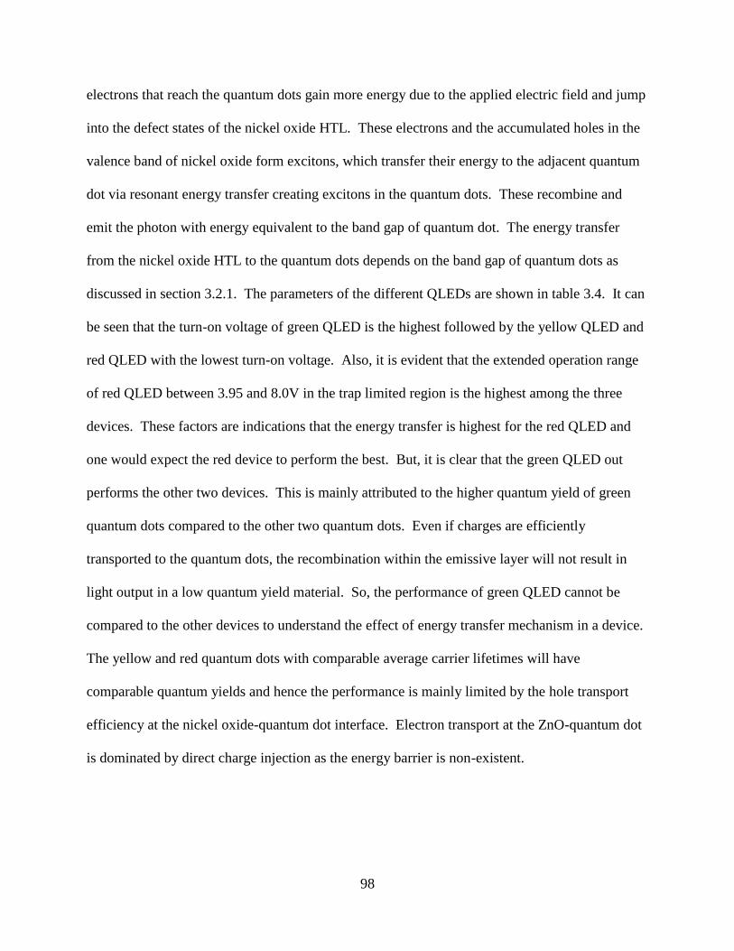
98
electrons that reach the quantum dots gain more energy due to the applied electric field and jump
into the defect states of the nickel oxide HTL. These electrons and the accumulated holes in the
valence band of nickel oxide form excitons, which transfer their energy to the adjacent quantum
dot via resonant energy transfer creating excitons in the quantum dots. These recombine and
emit the photon with energy equivalent to the band gap of quantum dot. The energy transfer
from the nickel oxide HTL to the quantum dots depends on the band gap of quantum dots as
discussed in section 3.2.1. The parameters of the different QLEDs are shown in table 3.4. It can
be seen that the turn-on voltage of green QLED is the highest followed by the yellow QLED and
red QLED with the lowest turn-on voltage. Also, it is evident that the extended operation range
of red QLED between 3.95 and 8.0V in the trap limited region is the highest among the three
devices. These factors are indications that the energy transfer is highest for the red QLED and
one would expect the red device to perform the best. But, it is clear that the green QLED out
performs the other two devices. This is mainly attributed to the higher quantum yield of green
quantum dots compared to the other two quantum dots. Even if charges are efficiently
transported to the quantum dots, the recombination within the emissive layer will not result in
light output in a low quantum yield material. So, the performance of green QLED cannot be
compared to the other devices to understand the effect of energy transfer mechanism in a device.
The yellow and red quantum dots with comparable average carrier lifetimes will have
comparable quantum yields and hence the performance is mainly limited by the hole transport
efficiency at the nickel oxide-quantum dot interface. Electron transport at the ZnO-quantum dot
is dominated by direct charge injection as the energy barrier is non-existent.
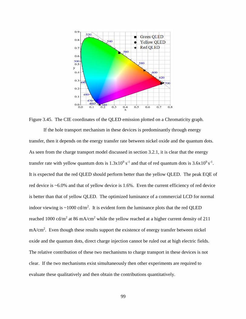
99
Figure 3.45. The CIE coordinates of the QLED emission plotted on a Chromaticity graph.
If the hole transport mechanism in these devices is predominantly through energy
transfer, then it depends on the energy transfer rate between nickel oxide and the quantum dots.
As seen from the charge transport model discussed in section 3.2.1, it is clear that the energy
transfer rate with yellow quantum dots is 1.3x10⁹ s-1 and that of red quantum dots is 3.6x10⁹ s-1.
It is expected that the red QLED should perform better than the yellow QLED. The peak EQE of
red device is ~6.0% and that of yellow device is 1.6%. Even the current efficiency of red device
is better than that of yellow QLED. The optimized luminance of a commercial LCD for normal
indoor viewing is ~1000 cd/m2. It is evident form the luminance plots that the red QLED
reached 1000 cd/m2 at 86 mA/cm2 while the yellow reached at a higher current density of 211
mA/cm2. Even though these results support the existence of energy transfer between nickel
oxide and the quantum dots, direct charge injection cannot be ruled out at high electric fields.
The relative contribution of these two mechanisms to charge transport in these devices is not
clear. If the two mechanisms exist simultaneously then other experiments are required to
evaluate these qualitatively and then obtain the contributions quantitatively.

100
Table 3.4. The performance parameters of the different all-inorganic QLEDs are tabled.
3.3.2. Hybrid QLED with PEDOT:PSS/nickel oxide nanoparticles HTL
3.3.2.1. Red emitting hybrid QLED
The band alignment of different device layers is shown in figure 3.46(a). The valence
and conduction band positions of zinc oxide and quantum dot emissive layers are taken from
literature [52]. The work function of FTO anode is reported to be 4.6-4.8 eV and that of Al
cathode is 4.28 eV. Hence, there is a ~ 0.2 eV barrier for electron injection at the Al-ZnO
interface. The PEDOT:PSS (poly(3,4-ethylenedioxythiophene) polystyrene sulfonate) is
ntroduced between the anode and the nickel oxide nanoparticle layer. This layer acts as a hole
injection layer (HIL), which reduces the hole barrier between anode and nickel oxide
nanoparticles from 1.5 eV to 1.0 eV. The valence band of nickel oxide nanoparticles is much
deeper than that of the nickel oxide thin film. This enables a very low barrier to injection of
holes at the nickel oxide nanoparticles-quantum dot interface. The barrier to hole injection is
around ~0.23 eV. The device operating at 9 V is shown in figure 3.46(b).
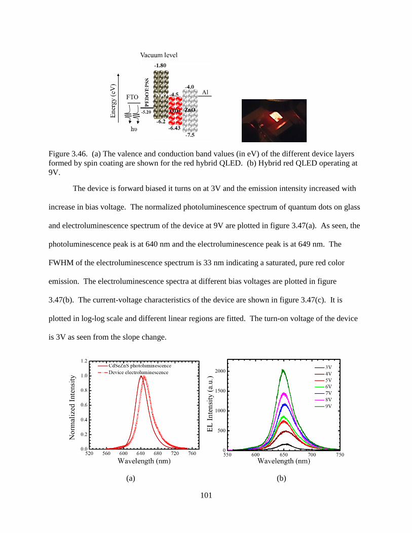
101
Figure 3.46. (a) The valence and conduction band values (in eV) of the different device layers
formed by spin coating are shown for the red hybrid QLED. (b) Hybrid red QLED operating at
9V.
The device is forward biased it turns on at 3V and the emission intensity increased with
increase in bias voltage. The normalized photoluminescence spectrum of quantum dots on glass
and electroluminescence spectrum of the device at 9V are plotted in figure 3.47(a). As seen, the
photoluminescence peak is at 640 nm and the electroluminescence peak is at 649 nm. The
FWHM of the electroluminescence spectrum is 33 nm indicating a saturated, pure red color
emission. The electroluminescence spectra at different bias voltages are plotted in figure
3.47(b). The current-voltage characteristics of the device are shown in figure 3.47(c). It is
plotted in log-log scale and different linear regions are fitted. The turn-on voltage of the device
is 3V as seen from the slope change.
(a) (b)

102
(c)
Figure 3.47. (a) The photoluminescence spectrum of the red quantum dots is compared to that of
the hybrid red QLED electroluminescence spectrum. (b) Electroluminescence of the hybrid
device at different bias voltages. (c) Current-voltage characteristic of red emitting hybrid
QLED.
The light output characteristics of the device are shown in figure. In figure 3.48(a), the
luminance of the device is plotted as a function of bias voltage. The luminance increases with
voltage and reaches a maximum of ~1800 cd/m2 at 9V. The voltage at which the device
luminance reaches 1000 cd/m2 is 6.76 V and corresponding current density is 436 mA/cm2. The
current and external quantum efficiencies of the device, plotted as a function of current density,
are shown in figure 3.48(b). Maximum current efficiency of 4.14 cd/A and EQE of 2.36% is
obtained at 129 mA/cm2 and corresponding forward voltage is 4.0V. Both current and quantum
efficiencies start to decrease after reaching the maximum value at 4.0V. Performance of these
devices is much lower than that of the all-inorganic devices with nickel oxide thin film. This is
due to the voids formed during the spin coating process. The nickel oxide nanoparticle powder
is not completely dispersed in the solvent as the quantum dots or ZnO nanoparticles. Hence,
forming a uniform, smooth film is difficult with the nickel oxide nanoparticles.

103
The working of this device is very close to that of commonly reported hybrid devices
with polymer or organic HIL/HTL. The charge transport in these devices is dominated by direct
charge injection process and there is no evidence of energy transfer. Direct hole injection form
HTL to quantum dots is possible as the nickel oxide nanoparticle HTL has a very deep valence
band at -6.2 eV close to the valence band of quantum dots. This also enables a much lower turn-
on voltage compared to the devices with nickel oxide thin film. The deep valence band is a
disadvantage as the barrier to hole injection from anode is increased. In order to reduce this
barrier, additional hole injection layer is inserted between the anode and the HTL. With a
polymer material the device is susceptible to damage from oxygen and moisture in the
atmosphere.
(a) (b)
Figure 3.48. (a) Luminance of the hybrid red QLED is plotted as a function of the bias voltage.
(b) The current efficiency and EQE of the hybrid device are plotted as a function of current
density.

104
4. CONCLUSION AND FUTURE WORK
4.1. Conclusion
In conclusion, efficient QLEDs with nickel oxide thin film and nickel oxide nanoparticles
are fabricated and characterized. The all-inorganic QLED with nickel oxide thin film HTL is
shown to operate by energy transfer mechanism between the HTL and quantum dots. The nickel
oxide thin film defect emission was engineered through non-stoichiometry of the film and
assigned based on structural, elemental and electrical properties of the nickel oxide film. It is
shown that the energy transfer is dependent on the spectral overlap of the quantum dot
absorbance with the nickel oxide thin film defect emission spectrum. It is evident form the
transfer time that energy transfer efficiency is maximum for the red quantum dots and reduces
with quantum dot size. This is due to the non-availability of resonant states between the nickel
oxide thin film HTL and smaller quantum dots. The performance of QLEDs with yellow and red
quantum dots clearly supports this charge transport model as the red QLED performed much
better than that of the yellow QLED. Even though the energy transfer efficiency is lower for the
green quantum dots, the green QLED with a maximum EQE of 11.4% performed the best
amongst the three types of QLEDs. This is mainly due to the high quantum yield of the green
quantum dots compared to the other quantum dots. It is clear from the transfer model that the
devices using red quantum dots with comparable quantum yield with blue quantum dots should
perform much better. The hybrid QLED with PEDOT:PSS/nickel oxide nanoparticle HIL/HTL
turns on at lower voltage than the all-inorganic QLEDs, but the performance is much lower.
Also, with a deep valence band of the nickel oxide nanoparticles the QLED predominantly
operates under charge injection mechanism.

105
4.2. Future work
It is anticipated that this resonant energy transfer property can be further exploited to
fabricate robust and efficient all-inorganic white LEDs with RGB quantum dots by further
engineering the trap states within the nickel oxide thin film bandgap to allow for spectral overlap
with RGB quantum dots. Further work is needed to determine exactly which quantum states are
populated by the energy transfer, and if this can be further controlled to improve the efficiency of
such devices. Moreover, new experiments are required to quantify the relative contributions of
energy transfer and direct charge injection mechanisms to the overall charge transport within the
QLED.

106
References
[1] L. Halonen, E. Tetri and P. Bhusal, Guidebook on Energy Efficient Electric Lighting for
Buildings. Aalto: Aalto University School of Science and Technology, 2010.
[2] D. Feldwinn, "The past, present and future of lighting", University of California, Santa
Barbara, 2017.
[3] R. Baldwin, "50 Years of LED Technology", WIRED, 2018. [Online]. Available:
https://www.wired.com/2012/10/the-history-of-led/. [Accessed: 28- Feb- 2018].
[4] "What is (IR)LED ?A light-emitting diode (LED) | DVR Unlimited", Blog.dvrunlimited.com,
2018. [Online]. Available: https://blog.dvrunlimited.com/archives/2499. [Accessed: 28- Feb-
2018].
[5] S. Dimitrijev, Principles of semiconductor devices, 2nd ed. New York: Oxford University
Press, 2012.
[6] D. Neamen, An introduction to semiconductor devices. Boston, Mass. [u.a.]: McGraw-Hill
Higher Education, 2008.
[7] "Fermi level and Fermi function", Hyperphysics.phy-astr.gsu.edu, 2018. [Online]. Available:
http://hyperphysics.phy-astr.gsu.edu/hbase/Solids/Fermi.html. [Accessed: 28- Feb- 2018].
[8] N. Holonyak and S. Bevacqua, "COHERENT (VISIBLE) LIGHT EMISSION FROM
Ga(As1−xPx) JUNCTIONS", Applied Physics Letters, vol. 1, no. 4, pp. 82-83, 1962.
[9] D. Ban, H. Luo, H. Liu, Z. Wasilewski, A. SpringThorpe, R. Glew and M. Buchanan,
"Optimized GaAs∕AlGaAs light-emitting diodes and high efficiency wafer-fused optical up-
conversion devices", Journal of Applied Physics, vol. 96, no. 9, pp. 5243-5248, 2004.
[10] S. Dutta Gupta and B. Jatothu, "Fundamentals and applications of light-emitting diodes
(LEDs) in in vitro plant growth and morphogenesis", Plant Biotechnology Reports, vol. 7,
no. 3, pp. 211-220, 2013.
[11] H. Jeong, R. Salas-Montiel, G. Lerondel and M. Jeong, "Indium gallium nitride-based
ultraviolet, blue, and green light-emitting diodes functionalized with shallow periodic hole
patterns", Scientific Reports, vol. 7, p. 45726, 2017.
[12] C. Skierbiszewski, P. Perlin, I. Grzegory, Z. Wasilewski, M. Siekacz, A. Feduniewicz, P.
Wisniewski, J. Borysiuk, P. Prystawko, G. Kamler, T. Suski and S. Porowski, "High power
blue–violet InGaN laser diodes grown on bulk GaN substrates by plasma-assisted molecular
beam epitaxy", Semiconductor Science and Technology, vol. 20, no. 8, pp. 809-813, 2005.
[13] S. Koizumi, "Ultraviolet Emission from a Diamond pn Junction", Science, vol. 292, no.
5523, pp. 1899-1901, 2001.
[14] Y. Taniyasu, M. Kasu and T. Makimoto, "An aluminium nitride light-emitting diode with a
wavelength of 210 nanometres", Nature, vol. 441, no. 7091, pp. 325-328, 2006.
107
[15] Y. Kubota, K. Watanabe, O. Tsuda and T. Taniguchi, "Deep Ultraviolet Light-Emitting
Hexagonal Boron Nitride Synthesized at Atmospheric Pressure”, ChemInform, vol. 38, no.
45, 2007.
[16] T. Dawson, "Development of efficient and durable sources of white light", Coloration
Technology, vol. 126, no. 1, pp. 1-10, 2010.
[17] T. Bosschaert, "Except Integrated Sustainability", Except Integrated Sustainability, 2018.
[Online]. Available: http://www.except.nl/en/articles/92-led-artificial-light-guide.
[Accessed: 28- Feb- 2018].
[18] A. Zukauskas, M. Shur and R. Gaska, Introduction to solid state lighting. New York: John
Wiley & Sons, 2002.
[19] D. A. Steigerwald et al., "Illumination with solid state lighting technology," in IEEE
Journal of Selected Topics in Quantum Electronics, vol. 8, no. 2, pp. 310-320, Mar/Apr
2002.
[20] B. Geffroy, P. le Roy and C. Prat, "Organic light-emitting diode (OLED) technology:
materials, devices and display technologies", Polymer International, vol. 55, no. 6, pp. 572-
582, 2006.
[21] J. Tremblay, "The rise of OLED displays | July 11, 2016 Issue - Vol. 94 Issue 28 | Chemical
& Engineering News", Cen.acs.org, 2018. [Online]. Available:
https://cen.acs.org/articles/94/i28/rise-OLED-displays.html. [Accessed: 28- Feb- 2018].
[22] S. Ho, S. Liu, Y. Chen and F. So, "Review of recent progress in multilayer solution-
processed organic light-emitting diodes", Journal of Photonics for Energy, vol. 5, no. 1, p.
057611, 2015.
[23] C. Sekine, Y. Tsubata, T. Yamada, M. Kitano and S. Doi, "Recent progress of high
performance polymer OLED and OPV materials for organic printed electronics", Science
and Technology of Advanced Materials, vol. 15, no. 3, p. 034203, 2014.
[24] R. Meerheim, S. Scholz, S. Olthof, G. Schwartz, S. Reineke, K. Walzer and K. Leo,
"Influence of charge balance and exciton distribution on efficiency and lifetime of
phosphorescent organic light-emitting devices", Journal of Applied Physics, vol. 104, no. 1,
p. 014510, 2008.
[25] Department of Energy, "Solid-State Lighting Research and Development", 2010.
[26] J. Caruge, J. Halpert, V. Bulović and M. Bawendi, "NiO as an Inorganic Hole-Transporting
Layer in Quantum-Dot Light-Emitting Devices", Nano Letters, vol. 6, no. 12, pp. 2991-
2994, 2006.
[27] J. Steckel, P. Snee, S. Coe-Sullivan, J. Zimmer, J. Halpert, P. Anikeeva, L. Kim, V. Bulovic
and M. Bawendi, "Color-Saturated Green-Emitting QD-LEDs", Angewandte Chemie
International Edition, vol. 45, no. 35, pp. 5796-5799, 2006.

108
[28] L. Swafford, L. Weigand, M. Bowers, J. McBride, J. Rapaport, T. Watt, S. Dixit, L.
Feldman and S. Rosenthal, "Homogeneously Alloyed CdSxSe1-xNanocrystals: Synthesis,
Characterization, and Composition/Size-Dependent Band Gap", Journal of the American
Chemical Society, vol. 128, no. 37, pp. 12299-12306, 2006.
[29] C. de Mello Donega, Nanoparticles. Berlin, Heidelberg: Springer Berlin Heidelberg, 2014,
pp. 13-51.
[30] V. Colvin, M. Schlamp and A. Alivisatos, "Light-emitting diodes made from cadmium
selenide nanocrystals and a semiconducting polymer", Nature, vol. 370, no. 6488, pp. 354-
357, 1994.
[31] B. Dabbousi, M. Bawendi, O. Onitsuka and M. Rubner, "Electroluminescence from CdSe
quantum‐dot/polymer composites", Applied Physics Letters, vol. 66, no. 11, pp. 1316-1318,
1995.
[32] H. Mattoussi, L. Radzilowski, B. Dabbousi, E. Thomas, M. Bawendi and M. Rubner,
"Electroluminescence from heterostructures of poly(phenylene vinylene) and inorganic
CdSe nanocrystals", Journal of Applied Physics, vol. 83, no. 12, pp. 7965-7974, 1998.
[33] S. Coe, W. Woo, M. Bawendi and V. Bulović, "Electroluminescence from single
monolayers of nanocrystals in molecular organic devices", Nature, vol. 420, no. 6917, pp.
800-803, 2002.
[34] A. Rizzo, M. Mazzeo, M. Palumbo, G. Lerario, S. D'Amone, R. Cingolani and G. Gigli,
"Hybrid Light-Emitting Diodes from Microcontact-Printing Double-Transfer of Colloidal
Semiconductor CdSe/ZnS Quantum Dots onto Organic Layers", Advanced Materials, vol.
20, no. 10, pp. 1886-1891, 2008.
[35] J. Stouwdam and R. Janssen, "Red, green, and blue quantum dot LEDs with solution
processable ZnO nanocrystal electron injection layers", Journal of Materials Chemistry, vol.
18, no. 16, p. 1889, 2008.
[36] B. Mashford, M. Stevenson, Z. Popovic, C. Hamilton, Z. Zhou, C. Breen, J. Steckel, V.
Bulovic, M. Bawendi, S. Coe-Sullivan and P. Kazlas, "High-efficiency quantum-dot light-
emitting devices with enhanced charge injection", Nature Photonics, vol. 7, no. 5, pp. 407-
412, 2013.
[37] Y. Yang, Y. Zheng, W. Cao, A. Titov, J. Hyvonen, J. Manders, J. Xue, P. Holloway and L.
Qian, "High-efficiency light-emitting devices based on quantum dots with tailored
nanostructures", Nature Photonics, vol. 9, no. 4, pp. 259-266, 2015.
[38] K. Acharya, A. Titov, J. Hyvonen, C. Wang, J. Tokarz and P. Holloway, "High efficiency
quantum dot light emitting diodes from positive aging", Nanoscale, vol. 9, no. 38, pp.
14451-14457, 2017.
[39] ]P. Anikeeva, C. Madigan, J. Halpert, M. Bawendi and V. Bulović, "Electronic and
excitonic processes in light-emitting devices based on organic materials and colloidal
quantum dots", Physical Review B, vol. 78, no. 8, 2008.

109
[40] L. Qian, Y. Zheng, J. Xue and P. Holloway, "Stable and efficient quantum-dot light-emitting
diodes based on solution-processed multilayer structures", Nature Photonics, vol. 5, no. 9,
pp. 543-548, 2011.
[41] J. Kwak, W. Bae, D. Lee, I. Park, J. Lim, M. Park, H. Cho, H. Woo, D. Yoon, K. Char, S.
Lee and C. Lee, "Bright and Efficient Full-Color Colloidal Quantum Dot Light-Emitting
Diodes Using an Inverted Device Structure", Nano Letters, vol. 12, no. 5, pp. 2362-2366,
2012.
[42] V. Wood, M. Panzer, J. Halpert, J. Caruge, M. Bawendi and V. Bulović, "Selection of Metal
Oxide Charge Transport Layers for Colloidal Quantum Dot LEDs", ACS Nano, vol. 3, no.
11, pp. 3581-3586, 2009.
[43] B. Mashford, T. Nguyen, G. Wilson and P. Mulvaney, "All-inorganic quantum-dot light-
emitting devices formed via low-cost, wet-chemical processing", J. Mater. Chem., vol. 20,
no. 1, pp. 167-172, 2010.
[44] S. Bhaumik and A. Pal, "All-Inorganic Light-Emitting Diodes Based on Solution-Processed
Nontoxic and Earth-Abundant Nanocrystals", IEEE Journal of Quantum Electronics, vol.
49, no. 3, pp. 325-330, 2013.
[45] H. Nguyen, N. Nguyen and S. Lee, "Application of solution-processed metal oxide layers as
charge transport layers for CdSe/ZnS quantum-dot LEDs", Nanotechnology, vol. 24, no. 11,
p. 115201, 2013.
[46] J. Caruge, J. Halpert, V. Bulović and M. Bawendi, "NiO as an Inorganic Hole-Transporting
Layer in Quantum-Dot Light-Emitting Devices", Nano Letters, vol. 6, no. 12, pp. 2991-
2994, 2006.
[47] X. Zhang, H. Dai, J. Zhao, C. Li, S. Wang and X. Sun, "Effects of the thickness of NiO hole
transport layer on the performance of all-inorganic quantum dot light emitting diode", Thin
Solid Films, vol. 567, pp. 72-76, 2014.
[48] J. Chen, Q. Huang, Q. Du, D. Zhao, F. Xu, J. Pan, W. Lei and A. Nathan, "Localized surface
plasmon resonance enhanced quantum dot light-emitting diodes via quantum dot-capped
gold nanoparticles", RSC Adv., vol. 4, no. 101, pp. 57574-57579, 2014.
[49] S. Bhaumik and A. Pal, "Light-Emitting Diodes Based on Solution-Processed Nontoxic
Quantum Dots: Oxides as Carrier-Transport Layers and Introducing Molybdenum Oxide
Nanoparticles as a Hole-Inject Layer", ACS Applied Materials & Interfaces, vol. 6, no. 14,
pp. 11348-11356, 2014.
[50] R. Vasan, H. Salman and M. O. Manasreh, "All inorganic quantum dot light emitting
devices with solution processed metal oxide transport layers", MRS Advances, vol. 1, no. 04,
pp. 305-310, 2016.
[51] W. Ji, S. Liu, H. Zhang, R. Wang, W. Xie and H. Zhang, "Ultrasonic Spray Processed,
Highly Efficient All-Inorganic Quantum-Dot Light-Emitting Diodes", ACS Photonics, vol.
4, no. 5, pp. 1271-1278, 2017.

110
[52] R. Vasan, H. Salman and M. O. Manasreh, "Solution Processed High Efficiency Quantum
Dot Light Emitting Diode with Inorganic Charge Transport Layers", IEEE Electron Device
Letters, vol. 39, no. 4, pp. 536-539, 2018.
[53] Y. Shirasaki, G. Supran, M. Bawendi and V. Bulović, "Emergence of colloidal quantum-dot
light-emitting technologies", Nature Photonics, vol. 7, no. 1, pp. 13-23, 2013.
[54] A. Efros, M. Rosen, M. Kuno, M. Nirmal, D. Norris and M. Bawendi, "Band-edge exciton
in quantum dots of semiconductors with a degenerate valence band: Dark and bright exciton
states", Physical Review B, vol. 54, no. 7, pp. 4843-4856, 1996.
[55] D. Talapin, I. Mekis, S. Goetzinger, A. Kornowski, O. Benson and H. Weller,
"CdSe/CdS/ZnS and CdSe/ZnSe/ZnS Core/Shell/Shell Nanocrystals", ChemInform, vol. 36,
no. 10, 2005.
[56] P. Reiss, J. Bleuse and A. Pron, "Highly Luminescent CdSe/ZnSe Core/Shell Nanocrystals
of Low Size Dispersion", Nano Letters, vol. 2, no. 7, pp. 781-784, 2002.
[57] W. Bae, K. Char, H. Hur and S. Lee, "Single-Step Synthesis of Quantum Dots with
Chemical Composition Gradients", Chemistry of Materials, vol. 20, no. 2, pp. 531-539,
2008.
[58] B. Kumar, R. Hue, W. Gladfelter and S. Campbell, "Comparing direct charge injection and
Forster energy transfer into quantum dots in hybrid organic/inorganic quantum dot light
emitting devices", Journal of Applied Physics, vol. 112, no. 3, p. 034501, 2012.
[59] B. Kumar, S. Campbell and P. Paul Ruden, "Modeling charge transport in quantum dot light
emitting devices with NiO and ZnO transport layers and Si quantum dots", Journal of
Applied Physics, vol. 114, no. 4, p. 044507, 2013.
[60] W. Bae, Y. Park, J. Lim, D. Lee, L. Padilha, H. McDaniel, I. Robel, C. Lee, J. Pietryga and
V. Klimov, "Controlling the influence of Auger recombination on the performance of
quantum-dot light-emitting diodes", Nature Communications, vol. 4, 2013.
[61] D. Bozyigit and V. Wood, "Challenges and solutions for high-efficiency quantum dot-based
LEDs", MRS Bulletin, vol. 38, no. 09, pp. 731-736, 2013.
[62] J. Manders, S. Tsang, M. Hartel, T. Lai, S. Chen, C. Amb, J. Reynolds and F. So, "Solution-
Processed Nickel Oxide Hole Transport Layers in High Efficiency Polymer Photovoltaic
Cells", Advanced Functional Materials, vol. 23, no. 23, pp. 2993-3001, 2013.
[63] S. Liu, R. Liu, Y. Chen, S. Ho, J. Kim and F. So, "Nickel Oxide Hole Injection/Transport
Layers for Efficient Solution-Processed Organic Light-Emitting Diodes", Chemistry of
Materials, vol. 26, no. 15, pp. 4528-4534, 2014.
[64] J. Li, Y. Shao, X. Chen, H. Wang, Y. Li and Q. Zhang, "All-inorganic quantum-dot light-
emitting-diodes with vertical nickel oxide nanosheets as hole transport layer", Progress in
Natural Science: Materials International, vol. 26, no. 5, pp. 503-509, 2016.

111
[65] N. Widjonarko, E. Ratcliff, C. Perkins, A. Sigdel, A. Zakutayev, P. Ndione, D. Gillaspie, D.
Ginley, D. Olson and J. Berry, "Sputtered nickel oxide thin film for efficient hole transport
layer in polymer–fullerene bulk-heterojunction organic solar cell", Thin Solid Films, vol.
520, no. 10, pp. 3813-3818, 2012.
[66] R. Srnanek, I. Hotovy, V. Malcher, A. Vincze, D. McPhail and S. Littlewood, "A Raman
study of NiOx films for gas sensors applications", ASDAM 2000. Conference Proceedings.
Third International Euro Conference on Advanced Semiconductor Devices and
Microsystems (Cat. No.00EX386), pp. 303-306, 2000.
[67] W. Bae, J. Kwak, J. Park, K. Char, C. Lee and S. Lee, "Highly Efficient Green-Light-
Emitting Diodes Based on CdSe@ZnS Quantum Dots with a Chemical-Composition
Gradient", Advanced Materials, vol. 21, no. 17, pp. 1690-1694, 2009.
[68] J. Zhou, Y. Liu, J. Tang and W. Tang, "Surface ligands engineering of semiconductor
quantum dots for chemosensory and biological applications", Materials Today, vol. 20, no.
7, pp. 360-376, 2017.
[69] S. Nalage, M. Chougule, S. Sen, P. Joshi and V. Patil, "Sol–gel synthesis of nickel oxide
thin films and their characterization", Thin Solid Films, vol. 520, no. 15, pp. 4835-4840,
2012.
[70] R. Vasan, F. Gao, M. O. Manasreh and C. Heyes, "Investigation of charge transport between
nickel oxide nanoparticles and CdSe/ZnS alloyed nanocrystals", MRS Advances, vol. 2, no.
51, pp. 2935-2941, 2017.
[71] T. Hirao, M. Furuta, T. Hiramatsu, T. Matsuda, C. Li, H. Furuta, H. Hokari, M. Yoshida, H.
Ishii and M. Kakegawa, "Bottom-Gate Zinc Oxide Thin-Film Transistors (ZnO TFTs) for
AM-LCDs", IEEE Transactions on Electron Devices, vol. 55, no. 11, pp. 3136-3142, 2008.
[72] X. Xu, Q. Cui, Y. Jin and X. Guo, "Low-voltage zinc oxide thin-film transistors with
solution-processed channel and dielectric layers below 150 °C", Applied Physics Letters,
vol. 101, no. 22, p. 222114, 2012.
[73] B. Omogo, F. Gao, P. Bajwa, M. Kaneko and C. Heyes, "Reducing Blinking in Small Core–
Multishell Quantum Dots by Carefully Balancing Confinement Potential and Induced
Lattice Strain: The “Goldilocks” Effect", ACS Nano, vol. 10, no. 4, pp. 4072-4082, 2016.
[74] F. Gao, A. Kreidermacher, I. Fritsch and C. Heyes, "3D Imaging of Flow Patterns in an
Internally-Pumped Microfluidic Device: Redox Magnetohydrodynamics and
Electrochemically-Generated Density Gradients", Analytical Chemistry, vol. 85, no. 9, pp.
4414-4422, 2013.
[75] H. Kuzmany, Solid-state spectroscopy, 2nd ed. Heidelberg: Springer, 2009, pp. 185-186.
[76] H. Kuzmany, Solid-state spectroscopy, 2nd ed. Heidelberg: Springer, 2009, pp. 314-316.
[77] D. Schroder, Semiconductor material and device characterization, 3rd ed. New York: John
Wiley & Sons, 2006, pp. 545-547.
112
[78] N. Durisic, A. Godin, D. Walters, P. Grütter, P. Wiseman and C. Heyes, "Probing the
“Dark” Fraction of Core–Shell Quantum Dots by Ensemble and Single Particle pH-
Dependent Spectroscopy", ACS Nano, vol. 5, no. 11, pp. 9062-9073, 2011.
[79] F. Gao, P. Bajwa, A. Nguyen and C. Heyes, "Shell-Dependent Photoluminescence Studies
Provide Mechanistic Insights into the Off–Grey–On Transitions of Blinking Quantum
Dots", ACS Nano, vol. 11, no. 3, pp. 2905-2916, 2017.
[80] F. Jiang, W. Choy, X. Li, D. Zhang and J. Cheng, "Post-treatment-Free Solution-Processed
Non-stoichiometric NiOx Nanoparticles for Efficient Hole-Transport Layers of Organic
Optoelectronic Devices", Advanced Materials, vol. 27, no. 18, pp. 2930-2937, 2015.
[81] F. Chiu, "A Review on Conduction Mechanisms in Dielectric Films", Advances in Materials
Science and Engineering, vol. 2014, pp. 1-18, 2014.
[82] V. Mihailetchi, J. Wildeman and P. Blom, "Space-Charge Limited Photocurrent", Physical
Review Letters, vol. 94, no. 12, pp. 6602-6604, 2005.
[83] S. Cheung and N. Cheung, "Extraction of Schottky diode parameters from forward current‐
voltage characteristics", Applied Physics Letters, vol. 49, no. 2, pp. 85-87, 1986.
[84] M. Stamataki, C. Sargentis, D. Tsamakis, I. Fasaki and M. Kompitsas, "Hydrogen gas
sensing application of Al/NiO Schottky diode", 2008 IEEE Sensors, pp. 843-846, 2008.
[85] R. Gupta, K. Ghosh and P. Kahol, "Fabrication and electrical characterization of Au/p-
Si/STO/Au contact", Current Applied Physics, vol. 9, no. 5, pp. 933-936, 2009.
[86] D. Schroder, Semiconductor material and device characterization, 3rd ed. New York: John
Wiley & Sons, 2006, pp. 160-162.
[87] K. Wang, J. Jeng, P. Shen, Y. Chang, E. Diau, C. Tsai, T. Chao, H. Hsu, P. Lin, P. Chen, T.
Guo and T. Wen, "p-type Mesoscopic Nickel Oxide/Organometallic Perovskite
Heterojunction Solar Cells", Scientific Reports, vol. 4, no. 1, 2014.
[88] M. Arefi and S. Rezaei-Zarchi, "Synthesis of Zinc Oxide Nanoparticles and Their Effect on
the Compressive Strength and Setting Time of Self-Compacted Concrete Paste as
Cementitious Composites", International Journal of Molecular Sciences, vol. 13, no. 12, pp.
4340-4350, 2012.
[89] T. Franzl, T. Klar, S. Schietinger, A. Rogach and J. Feldmann, "Exciton Recycling in
Graded Gap Nanocrystal Structures", Nano Letters, vol. 4, no. 9, pp. 1599-1603, 2004.
[90] C. Rowland, I. Fedin, H. Zhang, S. Gray, A. Govorov, D. Talapin and R. Schaller,
"Picosecond energy transfer and multiexciton transfer outpaces Auger recombination in
binary CdSe nanoplatelet solids", Nature Materials, vol. 14, no. 5, pp. 484-489, 2015.
[91] M. Achermann, M. Petruska, S. Crooker and V. Klimov, "Picosecond Energy Transfer in
Quantum Dot Langmuir−Blodgett Nanoassemblies", The Journal of Physical Chemistry B,
vol. 107, no. 50, pp. 13782-13787, 2003.
113
[92] T. Franzl, D. Koktysh, T. Klar, A. Rogach, J. Feldmann and N. Gaponik, "Fast energy
transfer in layer-by-layer assembled CdTe nanocrystal bilayers", Applied Physics Letters,
vol. 84, no. 15, pp. 2904-2906, 2004.
[93] P. Anikeeva, C. Madigan, S. Coe-Sullivan, J. Steckel, M. Bawendi and V. Bulović,
"Photoluminescence of CdSe/ZnS core/shell quantum dots enhanced by energy transfer
from a phosphorescent donor", Chemical Physics Letters, vol. 424, no. 1-3, pp. 120-125,
2006.
[94] K. Zheng, K. Žídek, M. Abdellah, W. Zhang, P. Chabera, N. Lenngren, A. Yartsev and T.
Pullerits, "Ultrafast Charge Transfer from CdSe Quantum Dots to p-Type NiO: Hole
Injection vs Hole Trapping", The Journal of Physical Chemistry C, vol. 118, no. 32, pp.
18462-18471, 2014.
[95] S. Yue, K. Liu, R. Xu, M. Li, M. Azam, K. Ren, J. Liu, Y. Sun, Z. Wang, D. Cao, X. Yan,
S. Qu, Y. Lei and Z. Wang, "Efficacious engineering on charge extraction for realizing
highly efficient perovskite solar cells", Energy & Environmental Science, vol. 10, no. 12,
pp. 2570-2578, 2017.
[96] X. Chang, W. Li, L. Zhu, H. Liu, H. Geng, S. Xiang, J. Liu and H. Chen, "Carbon-Based
CsPbBr3 Perovskite Solar Cells: All-Ambient Processes and High Thermal Stability", ACS
Applied Materials & Interfaces, vol. 8, no. 49, pp. 33649-33655, 2016.
[97] S. Forrest, D. Bradley and M. Thompson, "Measuring the Efficiency of Organic Light-
Emitting Devices", Advanced Materials, vol. 15, no. 13, pp. 1043-1048, 2003.
[98] Z. Tan, R. Moghaddam, M. Lai, P. Docampo, R. Higler, F. Deschler, M. Price, A.
Sadhanala, L. Pazos, D. Credgington, F. Hanusch, T. Bein, H. Snaith and R. Friend, "Bright
light-emitting diodes based on organometal halide perovskite", Nature Nanotechnology, vol.
9, no. 9, pp. 687-692, 2014.
[99] J. Pan, J. Chen, Q. Huang, L. Wang and W. Lei, "A highly efficient quantum dot light
emitting diode via improving the carrier balance by modulating the hole transport", RSC
Advances, vol. 7, no. 69, pp. 43366-43372, 2017.