design example report - power · . design example report . title . 100 w, low profile ... 10.2...
TRANSCRIPT

Power Integrations
5245 Hellyer Avenue, San Jose, CA 95138 USA. Tel: +1 408 414 9200 Fax: +1 408 414 9201
www.power.com
Design Example Report
Title 100 W, Low Profile (11 mm), Flyback DC-DC Converter Using TOPSw itchTM-JX TOP270VG
Specification 380 VDC Input; 24 V, 3 A; 12 V, 2.34 A Outputs
Application LCD TV
Author Applications Engineering Department
Document Number DER-299
Date August 3, 2015
Revision 1.4 Summary and Features • Highly energy efficient
• Full load efficiency >90% • Efficiency >89% above 10% load • Average efficiency >90% (25%, 50%, 75%, 100% load points) • Simplifies meeting ENERGY STAR 2.0 and EuP requirements
• Low cost, low component count and small PCB footprint solution • Performance met without synchronous output rectification • 132 kHz operation optimized core size and efficiency performance • Low profile eDIP™-12 package for ultra-slim designs
• Integrated protection and reliability features • Line under voltage lock out (UVLO) • Primary sensed output overvoltage shutdown (OVP). Latched OVP condition can be reset with a
fast AC reset circuit. • Auto recovery output over current (OCP) • Meets limited power source (LPS) <100 VA requirement with a single point of failure • Accurate thermal shutdown with large hysteresis
PATENT INFORMATION The products and applications illustrated herein (including transformer construction and circuits external to the products) may be covered by one or more U.S. and foreign patents, or potentially by pending U.S. and foreign patent applications assigned to Power Integrations. A complete list of Power Integrations' patents may be found at www.powerint.com. Power Integrations grants its customers a license under certain patent rights as set forth at <http://www.powerint.com/ip.htm>.

DER-299 100 W Flyback DC-DC Converter Using TOP270VG 03-Aug-15
Page 2 of 48
Power Integrations, Inc. Tel: +1 408 414 9200 Fax: +1 408 414 9201 www.power.com
Table of Contents 1 Introduction ......................................................................................................... 4 2 Power Supply Specification ................................................................................... 5 3 Schematic ............................................................................................................ 6 4 Circuit Description ................................................................................................ 7
4.1 TOPSwitch-JX Primary .................................................................................... 7 4.2 Output Rectification ....................................................................................... 7 4.3 Output Feedback ........................................................................................... 8 4.4 Fast AC Reset ................................................................................................ 8
5 PCB Layout .......................................................................................................... 9 6 Bill of Materials .................................................................................................. 11 7 Transformer Specification ................................................................................... 13
7.1 Electrical Diagram ........................................................................................ 13 7.2 Electrical Specifications ................................................................................ 13 7.3 Materials ..................................................................................................... 13 7.4 Comments ................................................................................................... 13 7.5 Transformer Build Diagram .......................................................................... 14 7.6 Winding Instructions .................................................................................... 15
8 Transformer Design Spreadsheet ........................................................................ 16 9 Heat Sink Assemblies .......................................................................................... 21
9.1 Diode Heat Sink ........................................................................................... 21 9.1.1 Diode Heat Sink Fabrication Drawing ...................................................... 21 9.1.2 Diode Heat Sink Assembly Drawing ........................................................ 22 9.1.3 Diode Heat Sink Assembly Pictures ......................................................... 23
9.2 TOPSwitch-JX Heat Sink ............................................................................... 24 9.2.1 TOPSwitch-JX Heat Sink Fabrication Drawing .......................................... 24 9.2.2 TOPSwitch-JX Heat Sink Assembly Drawing ............................................ 25 9.2.3 TOPSwitch-JX Heat Sink Assembly Pictures ............................................. 26
10 Performance Data ........................................................................................... 27 10.1 Full load Efficiency ....................................................................................... 27 10.2 Active Mode Efficiency ................................................................................. 29 10.3 No-Load Input Power ................................................................................... 30 10.4 Regulation ................................................................................................... 31
10.4.1 Load Regulation .................................................................................... 31 10.4.2 Line Regulation ..................................................................................... 33
10.5 Output Cross Regulation .............................................................................. 35 10.5.1 Cross Regulation Data ........................................................................... 35
11 Thermal Performance ...................................................................................... 36 11.1 Thermal Test Results at Room Temperature .................................................. 36 11.2 Thermal Scan at Room Temperature ............................................................. 37
12 Waveforms ..................................................................................................... 40 12.1 Drain Voltage and Current, Normal Operation ................................................ 40 12.2 Rectifier Peak Inverse Voltage (PIV) ............................................................. 41

03-Aug-15 DER-299 100 W Flyback DC-DC Converter Using TOP270VG
Page 3 of 48
Power Integrations Tel: +1 408 414 9200 Fax: +1 408 414 9201
www.power.com
12.3 Output OVP Profile (Simulated by Opening the Feedback Loop) ...................... 41 12.4 OCP Profile .................................................................................................. 42 12.5 Output Voltage Start-up Profile (Constant Resistance Mode)........................... 42 12.6 Load Transient Response (50% to 100% Load Step) ..................................... 43 12.7 Output Ripple Measurements ........................................................................ 44
12.7.1 Ripple Measurement Technique ............................................................. 44 12.7.2 Measurement Results ............................................................................ 45
13 Control Loop Measurements ............................................................................ 46 13.1 380 VDC Input Maximum Load ..................................................................... 46
14 Revision History .............................................................................................. 47 Important Note: Although this board is designed to satisfy safety isolation requirements, the engineering prototype has not been agency approved. Therefore, all testing should be performed using an isolated power source to provide the DC input to the prototype board.
DER-299 100 W Flyback DC-DC Converter Using TOP270VG 03-Aug-15
Page 4 of 48
Power Integrations, Inc. Tel: +1 408 414 9200 Fax: +1 408 414 9201 www.power.com
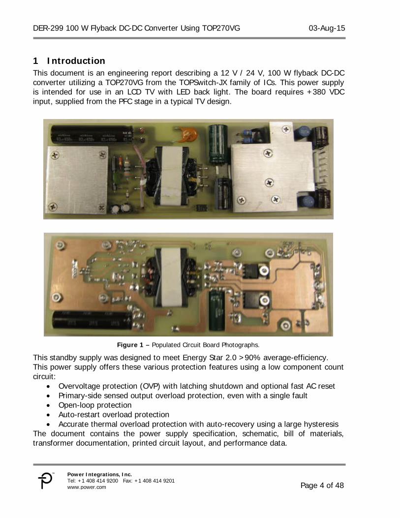
1 Introduction This document is an engineering report describing a 12 V / 24 V, 100 W flyback DC-DC converter utilizing a TOP270VG from the TOPSwitch-JX family of ICs. This power supply is intended for use in an LCD TV with LED back light. The board requires +380 VDC input, supplied from the PFC stage in a typical TV design.
Figure 1 – Populated Circuit Board Photographs.
This standby supply was designed to meet Energy Star 2.0 >90% average-efficiency. This power supply offers these various protection features using a low component count circuit:
• Overvoltage protection (OVP) with latching shutdown and optional fast AC reset • Primary-side sensed output overload protection, even with a single fault • Open-loop protection • Auto-restart overload protection • Accurate thermal overload protection with auto-recovery using a large hysteresis
The document contains the power supply specification, schematic, bill of materials, transformer documentation, printed circuit layout, and performance data.
03-Aug-15 DER-299 100 W Flyback DC-DC Converter Using TOP270VG
Page 5 of 48
Power Integrations Tel: +1 408 414 9200 Fax: +1 408 414 9201
www.power.com
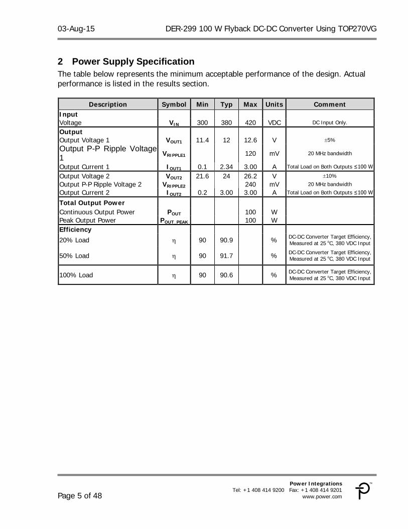
2 Power Supply Specification The table below represents the minimum acceptable performance of the design. Actual performance is listed in the results section.
Description Symbol Min Typ Max Units Comment Input Voltage VIN 300 380 420 VDC DC Input Only.
Output
Output Voltage 1 VOUT1 11.4 12 12.6 V ±5%
Output P-P Ripple Voltage 1 VRIPPLE1 120 mV 20 MHz bandwidth
Output Current 1 IOUT1 0.1 2.34 3.00 A Total Load on Both Outputs ≤100 W
Output Voltage 2 VOUT2 21.6 24 26.2 V ±10%
Output P-P Ripple Voltage 2 VRIPPLE2 240 mV 20 MHz bandwidth
Output Current 2 IOUT2 0.2 3.00 3.00 A Total Load on Both Outputs ≤100 W
Total Output Power
Continuous Output Power POUT 100 W
Peak Output Power POUT_PEAK 100 W
Efficiency
20% Load η 90 90.9 % DC-DC Converter Target Efficiency, Measured at 25 oC, 380 VDC Input
50% Load η 90 91.7 % DC-DC Converter Target Efficiency, Measured at 25 oC, 380 VDC Input
100% Load η 90 90.6 % DC-DC Converter Target Efficiency, Measured at 25 oC, 380 VDC Input

DER-299 100 W Flyback DC-DC Converter Using TOP270VG 03-Aug-15
Page 6 of 48
Power Integrations, Inc. Tel: +1 408 414 9200 Fax: +1 408 414 9201 www.power.com
3 Schematic
Figure 2 – Schematic.
Note: This design has an additional capacitor across the input terminals (C9) w hich represents the PFC stage output capacitor w hen used w ith a PFC stage.
Figure 3 – Fast AC Reset Circuit.

03-Aug-15 DER-299 100 W Flyback DC-DC Converter Using TOP270VG
Page 7 of 48
Power Integrations Tel: +1 408 414 9200 Fax: +1 408 414 9201
www.power.com
4 Circuit Description The schematic in Figure 2 depicts a 12 V / 24 V, 100 W flyback DC-DC converter intended for LCD TV applications.
4.1 TOPSw itch-JX Primary Resistors R12, R13 and R14 provide a current into the VOLTAGE MONITOR (V) pin of IC U3 proportional to the DC voltage across high-voltage bypass capacitor C9. An RCDZ clamp network (D3, R9, R10, C11 and VR1) limits the drain voltage of U3 to below 725 V after the power MOSFET inside U3 turns off. This configuration was selected as it maximizes efficiency across the load range. Diode D4 rectifies the output of the bias winding of transformer T1. Capacitor C13 filters the output of the bias winding. This provides the necessary bias supply for the optocoupler U1B. The secondary-side feedback circuitry maintains output voltage regulation via optocoupler U1. A change in current through the optocoupler diode causes a change in the current out of the optocoupler transistor (multiplied by the CTR of the optocoupler) and into CONTROL (C) pin of IC U3. Increasing current into the C pin reduces the duty cycle of the internal MOSFET thereby regulating the output voltage. Zener diode VR2 provides output overvoltage protection. Any fault condition which causes the power supply output to exceed regulation limits also causes the voltage across the bias winding to increase. Consequently, Zener diode VR2 breaks down and sufficient current flows into the V pin of U3 via D5 to exceed the OV shutdown threshold. A resistor can be added in series with VR2 that limits the current into the V pin and changes the latching to self-recovering OV shutdown. Resistor R11 programs the internal limit of U3.
4.2 Output Rectification Diode D1 provides rectification for the 24 V output, and low-ESR capacitor C3 provides filtering. A post filter consisting of inductor L1 and capacitor C6 reduce switching frequency ripple in power supply output. The snubber network comprised of resistors R1, R17 and C2 damp oscillations across diode D1 caused by the transformer winding leakage inductance and trace impedance thereby reducing radiated EMI and diode voltage stress.
DER-299 100 W Flyback DC-DC Converter Using TOP270VG 03-Aug-15
Page 8 of 48
Power Integrations, Inc. Tel: +1 408 414 9200 Fax: +1 408 414 9201 www.power.com
Diode D2 provides rectification for the 12 V output, and low-ESR capacitor C4 provides filtering. A post filter consisting of inductor L2 and capacitor C5 filter out the switching frequency ripple. The snubber network comprised of resistors R2, R18 and C1 damp oscillations on D2 caused by the transformer winding leakage inductance, reducing radiated EMI and diode voltage stress.
4.3 Output Feedback The output voltage is controlled using shunt regulator U2. Resistors R3, R4 and R8 sense the output voltage, forming a resistor divider connected to the reference input of IC U2. Changes in the output voltage and hence the voltage at the reference input of U2 results in changes in the cathode voltage of IC U2 and therefore optocoupler LED current. This changes the current into the C pin of U3 and acts to maintain output voltage regulation. Capacitor C8 introduces a pole at DC, rolling off the gain of U2. Resistor R7 and capacitor C7 provides an additional phase boost to achieve stable power supply operation. Resistor R5 sets the overall loop gain and limits current through U1A during transient conditions.
4.4 Fast AC Reset The TOPSwitch-JX family has a fast AC reset function which can be configured on the EXTERNAL CURRENT LIMIT (X) pin (as shown in Figure 3). Should the device stop switching due to a latching OVP fault condition, the circuit connected to the X pin will force IX to exceed IX(TH) = -27 µA (typical) and reset the latch when the AC input is disconnected or falls below a set threshold value. In Figure 3, R1, R2 and C1 set the time after AC is removed before the latch is reset. A higher gain BJT QR is desirable to allow a higher resistance value for R1 and lower capacitance value for C1, and thus minimize the circuit dissipation. Consult Application Note AN-47 TOPSwitch-JX Family Design Guide for further information.
03-Aug-15 DER-299 100 W Flyback DC-DC Converter Using TOP270VG
Page 9 of 48
Power Integrations Tel: +1 408 414 9200 Fax: +1 408 414 9201
www.power.com
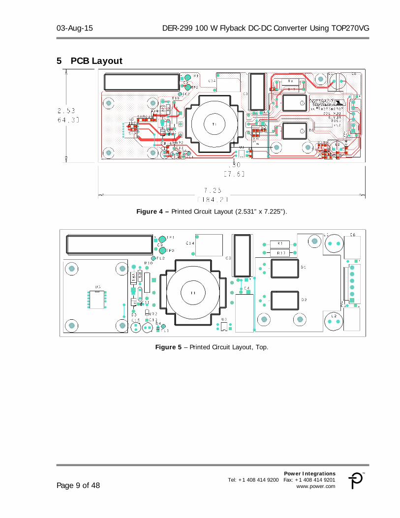
5 PCB Layout
Figure 4 – Printed Circuit Layout (2.531” x 7.225”).
Figure 5 – Printed Circuit Layout, Top.
DER-299 100 W Flyback DC-DC Converter Using TOP270VG 03-Aug-15
Page 10 of 48
Power Integrations, Inc. Tel: +1 408 414 9200 Fax: +1 408 414 9201 www.power.com
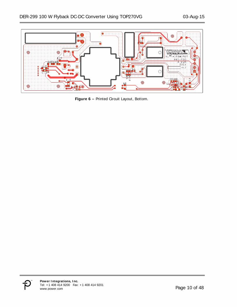
Figure 6 – Printed Circuit Layout, Bottom.
03-Aug-15 DER-299 100 W Flyback DC-DC Converter Using TOP270VG
Page 11 of 48
Power Integrations Tel: +1 408 414 9200 Fax: +1 408 414 9201
www.power.com
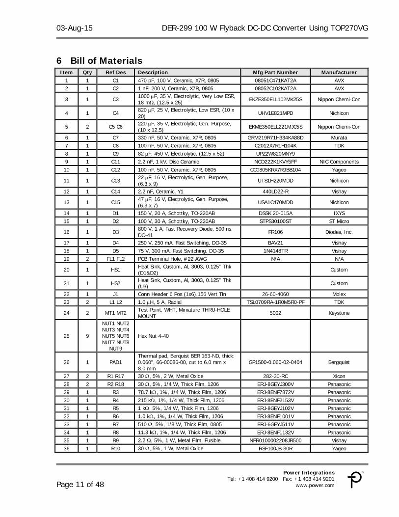
6 Bill of Materials Item Qty Ref Des Description Mfg Part Number Manufacturer
1 1 C1 470 pF, 100 V, Ceramic, X7R, 0805 08051C471KAT2A AVX 2 1 C2 1 nF, 200 V, Ceramic, X7R, 0805 08052C102KAT2A AVX
3 1 C3 1000 µF, 35 V, Electrolytic, Very Low ESR, 18 mΩ, (12.5 x 25) EKZE350ELL102MK25S Nippon Chemi-Con
4 1 C4 820 µF, 25 V, Electrolytic, Low ESR, (10 x 20) UHV1E821MPD Nichicon
5 2 C5 C6 220 µF, 35 V, Electrolytic, Gen. Purpose, (10 x 12.5) EKME350ELL221MJC5S Nippon Chemi-Con
6 1 C7 330 nF, 50 V, Ceramic, X7R, 0805 GRM219R71H334KA88D Murata 7 1 C8 100 nF, 50 V, Ceramic, X7R, 0805 C2012X7R1H104K TDK 8 1 C9 82 µF, 450 V, Electrolytic, (12.5 x 52) UPZ2W820MNY9 9 1 C11 2.2 nF, 1 kV, Disc Ceramic NCD222K1KVY5FF NIC Components 10 1 C12 100 nF, 50 V, Ceramic, X7R, 0805 CC0805KRX7R9BB104 Yageo
11 1 C13 22 µF, 16 V, Electrolytic, Gen. Purpose, (6.3 x 9) UTS1H220MDD Nichicon
12 1 C14 2.2 nF, Ceramic, Y1 440LD22-R Vishay
13 1 C15 47 µF, 16 V, Electrolytic, Gen. Purpose, (6.3 x 7) USA1C470MDD Nichicon
14 1 D1 150 V, 20 A, Schottky, TO-220AB DSSK 20-015A IXYS 15 1 D2 100 V, 30 A, Schottky, TO-220AB STPS30100ST ST Micro
16 1 D3 800 V, 1 A, Fast Recovery Diode, 500 ns, DO-41 FR106 Diodes, Inc.
17 1 D4 250 V, 250 mA, Fast Switching, DO-35 BAV21 Vishay 18 1 D5 75 V, 300 mA, Fast Switching, DO-35 1N4148TR Vishay 19 2 FL1 FL2 PCB Terminal Hole, #22 AWG N/A N/A
20 1 HS1 Heat Sink, Custom, Al, 3003, 0.125” Thk (D1&D2) Custom
21 1 HS2 Heat Sink, Custom, Al, 3003, 0.125” Thk (U3) Custom
22 1 J1 Conn Header 6 Pos (1x6).156 Vert Tin 26-60-4060 Molex 23 2 L1 L2 1.0 µH, 5 A, Radial TSL0709RA-1R0M5R0-PF TDK
24 2 MT1 MT2 Test Point, WHT, Miniature THRU-HOLE MOUNT 5002 Keystone
25 9
NUT1 NUT2 NUT3 NUT4 NUT5 NUT6 NUT7 NUT8
NUT9
Hex Nut 4-40
26 1 PAD1 Thermal pad, Berquist BER 163-ND, thick: 0.060", 66-00086-00, cut to 6.0 mm x 8.0 mm
GP1500-0.060-02-0404 Bergquist
27 2 R1 R17 30 Ω, 5%, 2 W, Metal Oxide 282-30-RC Xicon 28 2 R2 R18 30 Ω, 5%, 1/4 W, Thick Film, 1206 ERJ-8GEYJ300V Panasonic 29 1 R3 78.7 kΩ, 1%, 1/4 W, Thick Film, 1206 ERJ-8ENF7872V Panasonic 30 1 R4 215 kΩ, 1%, 1/4 W, Thick Film, 1206 ERJ-8ENF2153V Panasonic 31 1 R5 1 kΩ, 5%, 1/4 W, Thick Film, 1206 ERJ-8GEYJ102V Panasonic 32 1 R6 1.0 kΩ, 1%, 1/4 W, Thick Film, 1206 ERJ-8ENF1001V Panasonic 33 1 R7 510 Ω, 5%, 1/8 W, Thick Film, 0805 ERJ-6GEYJ511V Panasonic 34 1 R8 11.3 kΩ, 1%, 1/4 W, Thick Film, 1206 ERJ-8ENF1132V Panasonic 35 1 R9 2.2 Ω, 5%, 1 W, Metal Film, Fusible NFR0100002208JR500 Vishay 36 1 R10 30 Ω, 5%, 1 W, Metal Oxide RSF100JB-30R Yageo

DER-299 100 W Flyback DC-DC Converter Using TOP270VG 03-Aug-15
Page 12 of 48
Power Integrations, Inc. Tel: +1 408 414 9200 Fax: +1 408 414 9201 www.power.com
37 1 R11 12.7 kΩ, 1%, 1/4 W, Thick Film, 1206 ERJ-8ENF1272V Panasonic 38 1 R12 4.70 MΩ, 1%, 1/4 W, Thick Film, 1206 KTR18EZPF4704 Rohm Semi 39 1 R13 4.7 MΩ, 5%, 1/4 W, Thick Film, 1206 ERJ-8GEYJ475V Panasonic 40 1 R14 1.80 MΩ, 1%, 1/4 W, Thick Film, 1206 ERJ-8ENF1804V Panasonic 41 1 R15 6.8 Ω, 5%, 1/4 W, Thick Film, 1206 ERJ-8GEYJ6R8V Panasonic 42 1 R16 4.7 Ω, 5%, 1/8 W, Thick Film, 0805 ERJ-6GEYJ4R7V Panasonic
43 3 Spacer1 Spacer2 Spacer3
3/16”, STD Nylon spacer 561-KSP4 Eagle Plastic Devices
44 4
Spacer4 Spacer 5 Spacer6 Spacer7
SPACER ROUND #4 SCREW NYLON CLR 875 Keystone Electronics
45 6
SCREW1 SCREW2 SCREW3 SCREW4 SCREW5 SCREW6
SCREW MACHINE PHIL Flat head 4-40 X 7/16 SST Any RoHS Compliant
Mfg.
46 3 SCREW3 SCREW4 SCREW5
SCREW MACHINE PHIL Flat head 4-40 X 1/2 SST Any RoHS Compliant
Mfg.
47 1 T1 Bobbin, PQ38, Vertical, 6 pins BQ35/35-1112CPFR Pin Shine
48 2 TO-220
PAD1 TO-220 PAD2
THERMAL PAD TO-220 .009" SP1000 1009-58 Bergquist
49 1 TP1 Test Point, RED, THRU-HOLE MOUNT 5010 Keystone 50 1 TP2 Test Point, BLK, THRU-HOLE MOUNT 5011 Keystone 51 1 U1 Optocoupler, 35 V, CTR 80-160%, 4-DIP LTV-817A Liteon 52 1 U2 IC, REG ZENER SHUNT ADJ SOT-23 LM431AIM3/NOPB National Semi 53 1 U3 TOPSwitch-JX, eDIP-12P TOP270VG Power Integrations 54 1 VR1 200 V, 5 W, 5%, TVS, DO204AC (DO-15) P6KE200ARLG On Semi 55 1 VR2 28 V, 5%, 500 mW, DO-35 1N5255B-T Diodes, Inc.
56 2 WASHER1 WASHER2
Washer, Shoulder, #4, 0.095 Shoulder x 0.117 Dia, Polyphenylene Sulfide PPS 7721-10PPSG Aavid Thermalloy
57 2 WASHER3 WASHER4
Washer Flat #4 Zinc, OD 0.219, ID 0.125, Thk 0.032, Yellow Chromate Finish 5205820-2 Tyco

03-Aug-15 DER-299 100 W Flyback DC-DC Converter Using TOP270VG
Page 13 of 48
Power Integrations Tel: +1 408 414 9200 Fax: +1 408 414 9201
www.power.com
7 Transformer Specification
7.1 Electrical Diagram
Figure 7 – Transformer Electrical Diagram.
7.2 Electrical Specifications Electrical Strength 60 Hz 1 second, from pins 1, 2, 3, FL1, FL2 to pins 4, 5, 6. 3000 VAC
Primary Inductance
Measured at 1 V pk-pk, typical switching frequency, between pin 1 to pin 3, with all other windings open. 741 µH ±10%
Primary Leakage Inductance
Measured between pin 1 to pin 3, with all other windings shorted. 11.1 µH
7.3 Materials Item Description [1] Core: PQ3812, NC-2H (Nicera) or Equivalent, gapped for ALG of 666 nH/t² [2] Bobbin: Generic, 3 primary + 3 secondary [3] Barrier Tape: Polyester film [1 mil (25 µm) base thickness], 4.50 mm wide [4] Separation Tape: Barrier Tape: Polyester film [1 mil (25 µm) base thickness], 4.50 mm wide [5] Varnish [6] Magnet Wire: #26 AWG, Solderable Double Coated [7] Triple Insulated Wire: #25 AWG
7.4 Comments 1. Use of a grounded flux-band around the core may improve the EMI performance. 2. For non-margin wound transformers use triple insulated wire for all secondary windings.
DER-299 100 W Flyback DC-DC Converter Using TOP270VG 03-Aug-15
Page 14 of 48
Power Integrations, Inc. Tel: +1 408 414 9200 Fax: +1 408 414 9201 www.power.com
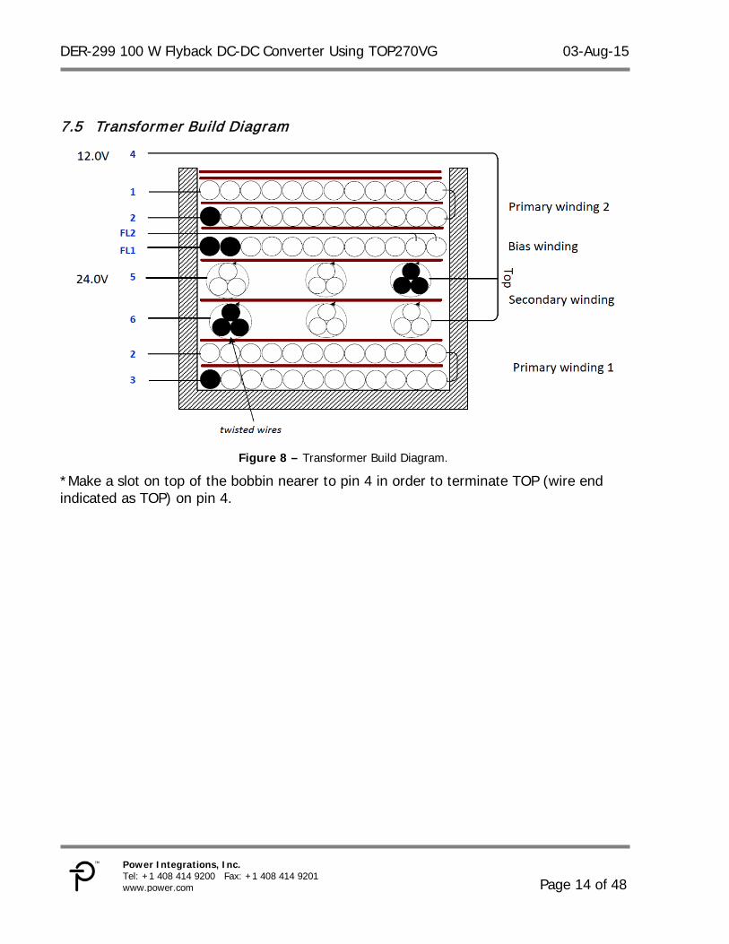
7.5 Transformer Build Diagram
Figure 8 – Transformer Build Diagram.
*Make a slot on top of the bobbin nearer to pin 4 in order to terminate TOP (wire end indicated as TOP) on pin 4.
03-Aug-15 DER-299 100 W Flyback DC-DC Converter Using TOP270VG
Page 15 of 48
Power Integrations Tel: +1 408 414 9200 Fax: +1 408 414 9201
www.power.com
7.6 Winding Instructions
Primary Winding (Section 1)
Start on pin(s) 3 and wind 17 turns (x 1 filar) of item [6] in 2 layer(s) from left to right. Add 1 layer of tape, item [4] in between each primary winding layer. At the end of 1st layer, continue to wind the next layer from right to left. On the final layer, spread the winding evenly across entire bobbin. Finish this winding on pin(s) 2. Add 1 layer of tape, item [3], for insulation.
Secondary Winding
Start on pin(s) 6 and wind 3 turns (x 3 filar) of item [7]. Spread the winding evenly across entire bobbin. Wind in same rotational direction as primary winding. Finish this winding on pin(s) TOP. Add 1 layer of tape, item [3], for insulation. Start on pin(s) TOP and wind 3 turns (x 3 filar) of item [7]. Spread the winding evenly across entire bobbin. Wind in same rotational direction as primary winding. Finish this winding on pin(s) 5. Add 1 layer of tape, item [3], for insulation.
Bias Winding
Start on pin(s) FL1* and wind 4 turns (x 2 filar) of item [6]. Wind in same rotational direction as primary winding. Spread the winding evenly across entire bobbin. Finish this winding on pin(s) FL2*. Add 1 layer of tape, item [3], for insulation.
Primary Winding (Section 2)
Start on pin(s) 2 and wind 16 turns (x 1 filar) of item [6] in 2 layer(s) from left to right. Add 1 layer of tape, item [4] in between each primary winding layer. At the end of 1st layer, continue to wind the next layer from right to left. On the final layer, spread the winding evenly across entire bobbin. Finish this winding on pin(s) 1. Add 3 layers of tape, item [3], for insulation.
TOP Terminate wire end indicated as TOP on pin(s) 4.
Core Assembly Adjust inductance of primary winding across terminals 1 and 3 of the transformer by grinding the center limb of the transformer core. Assemble and secure core halves. Item [1].
Varnish Dip varnish uniformly in item [5]. Do not vacuum impregnate.
DER-299 100 W Flyback DC-DC Converter Using TOP270VG 03-Aug-15
Page 16 of 48
Power Integrations, Inc. Tel: +1 408 414 9200 Fax: +1 408 414 9201 www.power.com
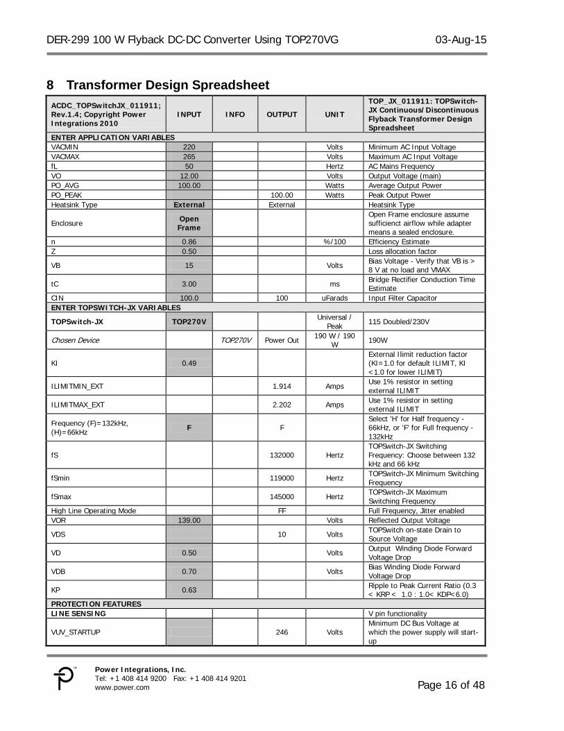
8 Transformer Design Spreadsheet ACDC_TOPSwitchJX_011911; Rev.1.4; Copyright Power Integrations 2010
INPUT INFO OUTPUT UNIT
TOP_JX_011911: TOPSwitch-JX Continuous/Discontinuous Flyback Transformer Design Spreadsheet
ENTER APPLICATION VARIABLES VACMIN 220 Volts Minimum AC Input Voltage VACMAX 265 Volts Maximum AC Input Voltage fL 50 Hertz AC Mains Frequency VO 12.00 Volts Output Voltage (main) PO_AVG 100.00 Watts Average Output Power PO_PEAK 100.00 Watts Peak Output Power Heatsink Type External External Heatsink Type
Enclosure Open Frame
Open Frame enclosure assume sufficienct airflow while adapter means a sealed enclosure.
n 0.86 %/100 Efficiency Estimate Z 0.50 Loss allocation factor
VB 15 Volts Bias Voltage - Verify that VB is > 8 V at no load and VMAX
tC 3.00 ms Bridge Rectifier Conduction Time Estimate
CIN 100.0 100 uFarads Input Filter Capacitor ENTER TOPSWITCH-JX VARIABLES
TOPSwitch-JX TOP270V Universal / Peak 115 Doubled/230V
Chosen Device TOP270V Power Out 190 W / 190 W 190W
KI 0.49 External Ilimit reduction factor (KI=1.0 for default ILIMIT, KI <1.0 for lower ILIMIT)
ILIMITMIN_EXT 1.914 Amps Use 1% resistor in setting external ILIMIT
ILIMITMAX_EXT 2.202 Amps Use 1% resistor in setting external ILIMIT
Frequency (F)=132kHz, (H)=66kHz F F
Select 'H' for Half frequency - 66kHz, or 'F' for Full frequency - 132kHz
fS 132000 Hertz TOPSwitch-JX Switching Frequency: Choose between 132 kHz and 66 kHz
fSmin 119000 Hertz TOPSwitch-JX Minimum Switching Frequency
fSmax 145000 Hertz TOPSwitch-JX Maximum Switching Frequency
High Line Operating Mode FF Full Frequency, Jitter enabled VOR 139.00 Volts Reflected Output Voltage
VDS 10 Volts TOPSwitch on-state Drain to Source Voltage
VD 0.50 Volts Output Winding Diode Forward Voltage Drop
VDB 0.70 Volts Bias Winding Diode Forward Voltage Drop
KP 0.63 Ripple to Peak Current Ratio (0.3 < KRP < 1.0 : 1.0< KDP<6.0)
PROTECTION FEATURES LINE SENSING V pin functionality
VUV_STARTUP 246 Volts Minimum DC Bus Voltage at which the power supply will start-up

03-Aug-15 DER-299 100 W Flyback DC-DC Converter Using TOP270VG
Page 17 of 48
Power Integrations Tel: +1 408 414 9200 Fax: +1 408 414 9201
www.power.com
VOV_SHUTDOWN 1252 Volts Typical DC Bus Voltage at which power supply will shut-down (Max)
RLS 11.2 M-ohms Use two standard, 5.6 M-Ohm, 5% resistors in series for line sense functionality.
OUTPUT OVERVOLTAGE
VZ 27 Volts Zener Diode rated voltage for Output Overvoltage shutdown protection
RZ 5.1 k-ohms Output OVP resistor. For latching shutdown use 20 ohm resistor instead
OVERLOAD POWER LIMITING X pin functionality
Overload Current Ratio at VMAX 1.2
Enter the desired margin to current limit at VMAX. A value of 1.2 indicates that the current limit should be 20% higher than peak primary current at VMAX
Overload Current Ratio at VMIN 1.09 Margin to current limit at low line. ILIMIT_EXT_VMIN 1.78 A Peak primary Current at VMIN ILIMIT_EXT_VMAX 1.71 A Peak Primary Current at VMAX
RIL 12.52 k-ohms Current limit/Power Limiting resistor.
RPL N/A M-ohms Resistor not required. Use RIL resistor only
ENTER TRANSFORMER CORE/CONSTRUCTION VARIABLES Core Type PQ3812 PQ3812 Core Type Core #N/A P/N: #N/A Bobbin #N/A P/N: #N/A
AE 1.2900 1.29 cm^2 Core Effective Cross Sectional Area
LE 4.3500 4.35 cm Core Effective Path Length
AL 4000.0 4000 nH/T^2 Ungapped Core Effective Inductance
BW 4.5 4.5 mm Bobbin Physical Winding Width
M 0.00 mm Safety Margin Width (Half the Primary to Secondary Creepage Distance)
L 4.00 Number of Primary Layers NS 3 3 Number of Secondary Turns DC INPUT VOLTAGE PARAMETERS VMIN 284 Volts Minimum DC Input Voltage VMAX 380 380 Volts Maximum DC Input Voltage CURRENT WAVEFORM SHAPE PARAMETERS
DMAX 0.34 Maximum Duty Cycle (calculated at PO_PEAK)
IAVG 0.41 Amps Average Primary Current (calculated at average output power)
IP 1.78 Amps Peak Primary Current (calculated at Peak output power)
IR 1.12 Amps Primary Ripple Current (calculated at average output power)
IRMS 0.73 Amps Primary RMS Current (calculated at average output power)
TRANSFORMER PRIMARY DESIGN PARAMETERS LP 741 uHenries Primary Inductance LP Tolerance 10 Tolerance of Primary Inductance NP 33 Primary Winding Number of Turns
DER-299 100 W Flyback DC-DC Converter Using TOP270VG 03-Aug-15
Page 18 of 48
Power Integrations, Inc. Tel: +1 408 414 9200 Fax: +1 408 414 9201 www.power.com
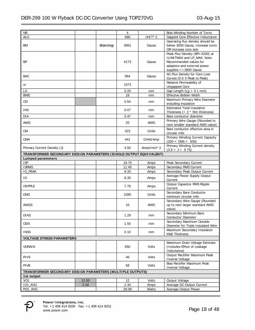
NB 4 Bias Winding Number of Turns ALG 666 nH/T^2 Gapped Core Effective Inductance
BM Warning 3061 Gauss Operating flux density should be below 3000 Gauss, Increase turns OR increase core size
BP 4173 Gauss
Peak Flux Density (BP<4200) at ILIMITMAX and LP_MAX. Note: Recommended values for adapters and external power supplies <=3600 Gauss
BAC 964 Gauss AC Flux Density for Core Loss Curves (0.5 X Peak to Peak)
ur 1073 Relative Permeability of Ungapped Core
LG 0.20 mm Gap Length (Lg > 0.1 mm) BWE 18 mm Effective Bobbin Width
OD 0.54 mm Maximum Primary Wire Diameter including insulation
INS 0.07 mm Estimated Total Insulation Thickness (= 2 * film thickness)
DIA 0.47 mm Bare conductor diameter
AWG 25 AWG Primary Wire Gauge (Rounded to next smaller standard AWG value)
CM 323 Cmils Bare conductor effective area in circular mils
CMA 441 Cmils/Amp Primary Winding Current Capacity (200 < CMA < 500)
Primary Current Density (J) 4.50 Amps/mm^2 Primary Winding Current density (3.8 < J < 9.75)
TRANSFORMER SECONDARY DESIGN PARAMETERS (SINGLE OUTPUT EQUIVALENT) Lumped parameters ISP 19.75 Amps Peak Secondary Current ISRMS 11.40 Amps Secondary RMS Current IO_PEAK 8.33 Amps Secondary Peak Output Current
IO 8.33 Amps Average Power Supply Output Current
IRIPPLE 7.78 Amps Output Capacitor RMS Ripple Current
CMS 2280 Cmils Secondary Bare Conductor minimum circular mils
AWGS 16 AWG Secondary Wire Gauge (Rounded up to next larger standard AWG value)
DIAS 1.29 mm Secondary Minimum Bare Conductor Diameter
ODS 1.50 mm Secondary Maximum Outside Diameter for Triple Insulated Wire
INSS 0.10 mm Maximum Secondary Insulation Wall Thickness
VOLTAGE STRESS PARAMETERS
VDRAIN 650 Volts Maximum Drain Voltage Estimate (Includes Effect of Leakage Inductance)
PIVS 46 Volts Output Rectifier Maximum Peak Inverse Voltage
PIVB 58 Volts Bias Rectifier Maximum Peak Inverse Voltage
TRANSFORMER SECONDARY DESIGN PARAMETERS (MULTIPLE OUTPUTS) 1st output VO1 12.00 12 Volts Output Voltage IO1_AVG 2.34 2.34 Amps Average DC Output Current PO1_AVG 28.08 Watts Average Output Power
03-Aug-15 DER-299 100 W Flyback DC-DC Converter Using TOP270VG
Page 19 of 48
Power Integrations Tel: +1 408 414 9200 Fax: +1 408 414 9201
www.power.com
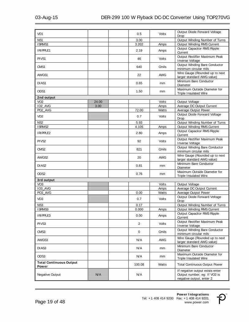
VD1 0.5 Volts Output Diode Forward Voltage Drop
NS1 3.00 Output Winding Number of Turns ISRMS1 3.202 Amps Output Winding RMS Current
IRIPPLE1 2.19 Amps Output Capacitor RMS Ripple Current
PIVS1 46 Volts Output Rectifier Maximum Peak Inverse Voltage
CMS1 640 Cmils Output Winding Bare Conductor minimum circular mils
AWGS1 22 AWG Wire Gauge (Rounded up to next larger standard AWG value)
DIAS1 0.65 mm Minimum Bare Conductor Diameter
ODS1 1.50 mm Maximum Outside Diameter for Triple Insulated Wire
2nd output VO2 24.00 Volts Output Voltage IO2_AVG 3.00 Amps Average DC Output Current PO2_AVG 72.00 Watts Average Output Power
VD2 0.7 Volts Output Diode Forward Voltage Drop
NS2 5.93 Output Winding Number of Turns ISRMS2 4.105 Amps Output Winding RMS Current
IRIPPLE2 2.80 Amps Output Capacitor RMS Ripple Current
PIVS2 92 Volts Output Rectifier Maximum Peak Inverse Voltage
CMS2 821 Cmils Output Winding Bare Conductor minimum circular mils
AWGS2 20 AWG Wire Gauge (Rounded up to next larger standard AWG value)
DIAS2 0.81 mm Minimum Bare Conductor Diameter
ODS2 0.76 mm Maximum Outside Diameter for Triple Insulated Wire
3rd output VO3 Volts Output Voltage IO3_AVG Amps Average DC Output Current PO3_AVG 0.00 Watts Average Output Power
VD3 0.7 Volts Output Diode Forward Voltage Drop
NS3 0.17 Output Winding Number of Turns ISRMS3 0.000 Amps Output Winding RMS Current
IRIPPLE3 0.00 Amps Output Capacitor RMS Ripple Current
PIVS3 2 Volts Output Rectifier Maximum Peak Inverse Voltage
CMS3 0 Cmils Output Winding Bare Conductor minimum circular mils
AWGS3 N/A AWG Wire Gauge (Rounded up to next larger standard AWG value)
DIAS3 N/A mm Minimum Bare Conductor Diameter
ODS3 N/A mm Maximum Outside Diameter for Triple Insulated Wire
Total Continuous Output Power 100.08 Watts Total Continuous Output Power
Negative Output N/A N/A If negative output exists enter Output number; eg: If VO2 is negative output, enter 2

DER-299 100 W Flyback DC-DC Converter Using TOP270VG 03-Aug-15
Page 20 of 48
Power Integrations, Inc. Tel: +1 408 414 9200 Fax: +1 408 414 9201 www.power.com
Note: Operating flux density of the transformer has slightly exceeded its maximum value because of maximum height limitation on the board. It cannot be increased any further.

03-Aug-15 DER-299 100 W Flyback DC-DC Converter Using TOP270VG
Page 21 of 48
Power Integrations Tel: +1 408 414 9200 Fax: +1 408 414 9201
www.power.com
9 Heat Sink Assemblies
9.1 Diode Heat Sink
9.1.1 Diode Heat Sink Fabrication Drawing
Figure 9 – Heat Sink Fabrication Drawing for D1 and D2.
DER-299 100 W Flyback DC-DC Converter Using TOP270VG 03-Aug-15
Page 22 of 48
Power Integrations, Inc. Tel: +1 408 414 9200 Fax: +1 408 414 9201 www.power.com
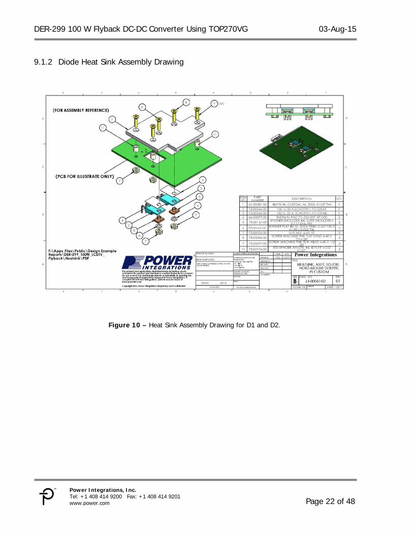
9.1.2 Diode Heat Sink Assembly Drawing
Figure 10 – Heat Sink Assembly Drawing for D1 and D2.

03-Aug-15 DER-299 100 W Flyback DC-DC Converter Using TOP270VG
Page 23 of 48
Power Integrations Tel: +1 408 414 9200 Fax: +1 408 414 9201
www.power.com
9.1.3 Diode Heat Sink Assembly Pictures
Figure 11 – Heat sink Sample. Figure 12 – Install Diodes D1 and D2 Onto Heat
Sink.
Figure 13 – Top. Side Figure 14 – Bottom Side.

DER-299 100 W Flyback DC-DC Converter Using TOP270VG 03-Aug-15
Page 24 of 48
Power Integrations, Inc. Tel: +1 408 414 9200 Fax: +1 408 414 9201 www.power.com
9.2 TOPSw itch-JX Heat Sink
9.2.1 TOPSwitch-JX Heat Sink Fabrication Drawing
Figure 15 – Heat Sink Fabrication Drawing for TOPSwitch-JX.
03-Aug-15 DER-299 100 W Flyback DC-DC Converter Using TOP270VG
Page 25 of 48
Power Integrations Tel: +1 408 414 9200 Fax: +1 408 414 9201
www.power.com
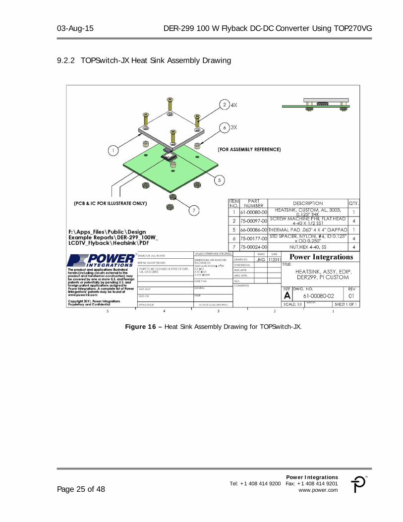
9.2.2 TOPSwitch-JX Heat Sink Assembly Drawing
Figure 16 – Heat Sink Assembly Drawing for TOPSwitch-JX.

DER-299 100 W Flyback DC-DC Converter Using TOP270VG 03-Aug-15
Page 26 of 48
Power Integrations, Inc. Tel: +1 408 414 9200 Fax: +1 408 414 9201 www.power.com
9.2.3 TOPSwitch-JX Heat Sink Assembly Pictures
Figure 17 – Heat sink Sample.
Figure 18 – Top. Figure 19 – Bottom side Note: A 6 mm x 8 mm piece of Bergquist thermal pad is installed on the top surface of IC U3 prior to installation of the heat sink.

03-Aug-15 DER-299 100 W Flyback DC-DC Converter Using TOP270VG
Page 27 of 48
Power Integrations Tel: +1 408 414 9200 Fax: +1 408 414 9201
www.power.com
10 Performance Data All measurements performed at room temperature.
10.1 Full load Efficiency Efficiency data points were recorded after 30 minutes soak time at 25 ºC ambient.
90.0
90.1
90.2
90.3
90.4
90.5
90.6
90.7
90.8
90.9
91.0
270 280 290 300 310 320 330 340 350 360 370 380 390 400 410
Effic
ienc
y (%
)
Input Voltage (VDC)
Figure 20 – Efficiency vs. Line Voltage, Full Load, Room Temperature.

DER-299 100 W Flyback DC-DC Converter Using TOP270VG 03-Aug-15
Page 28 of 48
Power Integrations, Inc. Tel: +1 408 414 9200 Fax: +1 408 414 9201 www.power.com
VIN (V)
PIN (W)
VOUT(24 V) (V)
IOUT(24
V) (A) VOUT(12
V) (V) IOUT(12
V) (A) Efficiency
(%) 280 110.51 24.03 3.011 11.886 2.338 90.61967 290 110.46 24.03 3.011 11.887 2.338 90.66281 300 110.45 24.03 3.011 11.887 2.338 90.67101 310 110.44 24.03 3.011 11.888 2.338 90.68134 320 110.44 24.03 3.011 11.89 2.338 90.68558 330 110.44 24.02 3.011 11.89 2.338 90.65831 340 110.45 24.02 3.011 11.891 2.338 90.65222 350 110.48 24.01 3.011 11.892 2.338 90.60247 360 110.51 24.01 3.011 11.892 2.338 90.57787 370 110.53 24.01 3.011 11.893 2.338 90.5636 380 110.56 24.01 3.011 11.894 2.338 90.54114 390 110.6 24.01 3.011 11.895 2.338 90.51051 400 110.71 24.01 3.011 11.898 2.338 90.42691
Table 1 – Efficiency Data with Line Voltage Variation at Full Load.
03-Aug-15 DER-299 100 W Flyback DC-DC Converter Using TOP270VG
Page 29 of 48
Power Integrations Tel: +1 408 414 9200 Fax: +1 408 414 9201
www.power.com
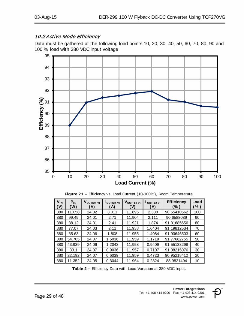
10.2 Active Mode Efficiency Data must be gathered at the following load points 10, 20, 30, 40, 50, 60, 70, 80, 90 and 100 % load with 380 VDC input voltage
85
86
87
88
89
90
91
92
93
94
95
0 10 20 30 40 50 60 70 80 90 100
Effic
ienc
y (%
)
Load Current (%)
Figure 21 – Efficiency vs. Load Current (10-100%), Room Temperature.
VIN (V)
PIN (W)
VOUT(24 V) (V)
IOUT(24 V) (A)
VOUT(12 V)
(V) IOUT(12 V)
(A) Efficiency
(%) Load (%)
380 110.58 24.02 3.011 11.895 2.338 90.55410562 100 380 99.49 24.01 2.71 11.904 2.111 90.6588039 90 380 88.12 24.01 2.41 11.921 1.874 91.01685656 80 380 77.07 24.03 2.11 11.938 1.6404 91.19812534 70 380 65.63 24.06 1.808 11.955 1.4084 91.93646503 60 380 54.705 24.07 1.5036 11.959 1.1719 91.77662755 50 380 43.939 24.06 1.2043 11.958 0.9409 91.55133298 40 380 33.1 24.07 0.9036 11.957 0.7107 91.38215076 30 380 22.192 24.07 0.6039 11.959 0.4723 90.95218412 20 380 11.352 24.05 0.3044 11.964 0.2324 88.9821494 10
Table 2 – Efficiency Data with Load Variation at 380 VDC Input.
DER-299 100 W Flyback DC-DC Converter Using TOP270VG 03-Aug-15
Page 30 of 48
Power Integrations, Inc. Tel: +1 408 414 9200 Fax: +1 408 414 9201 www.power.com
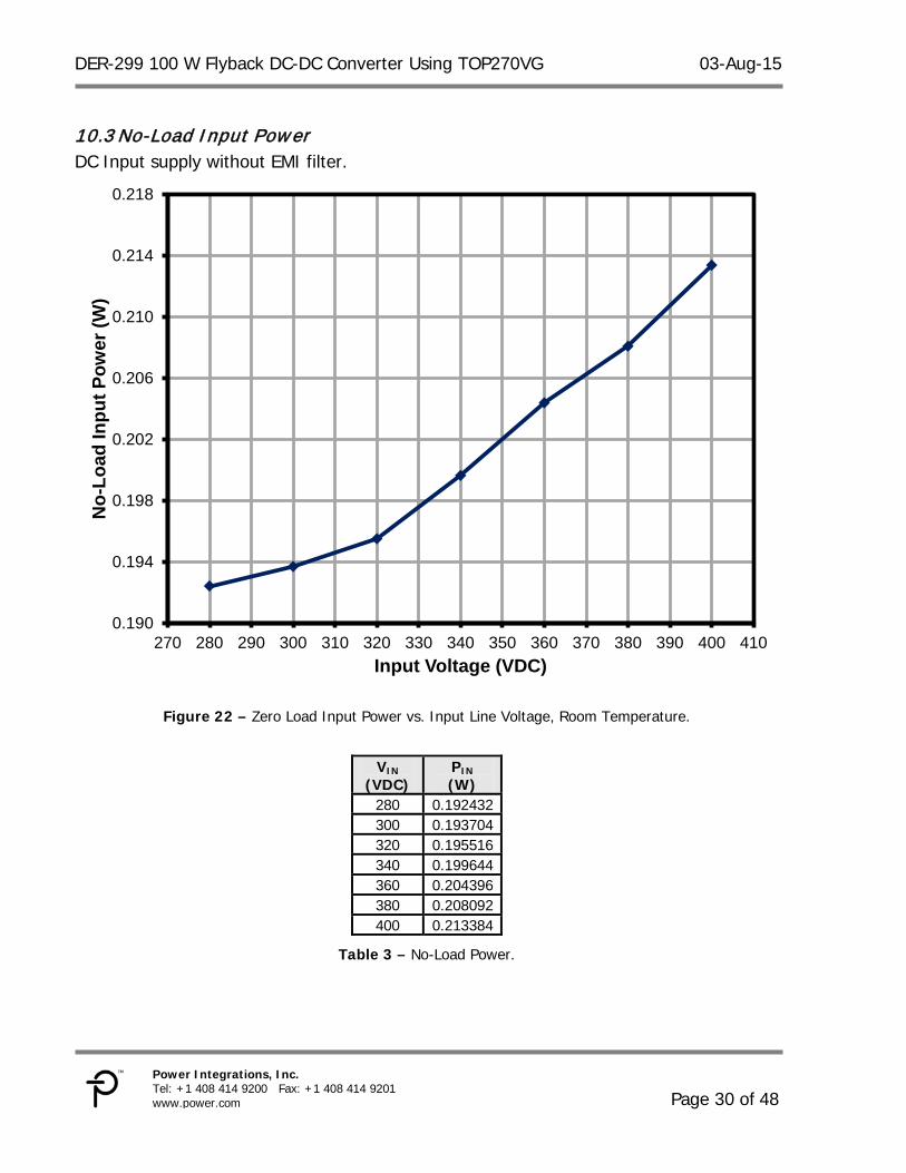
10.3 No-Load Input Power DC Input supply without EMI filter.
0.190
0.194
0.198
0.202
0.206
0.210
0.214
0.218
270 280 290 300 310 320 330 340 350 360 370 380 390 400 410
No -
Load
Inpu
t Pow
er (W
)
Input Voltage (VDC)
Figure 22 – Zero Load Input Power vs. Input Line Voltage, Room Temperature.
VIN
(VDC) PIN (W)
280 0.192432 300 0.193704 320 0.195516 340 0.199644 360 0.204396 380 0.208092 400 0.213384
Table 3 – No-Load Power.
03-Aug-15 DER-299 100 W Flyback DC-DC Converter Using TOP270VG
Page 31 of 48
Power Integrations Tel: +1 408 414 9200 Fax: +1 408 414 9201
www.power.com
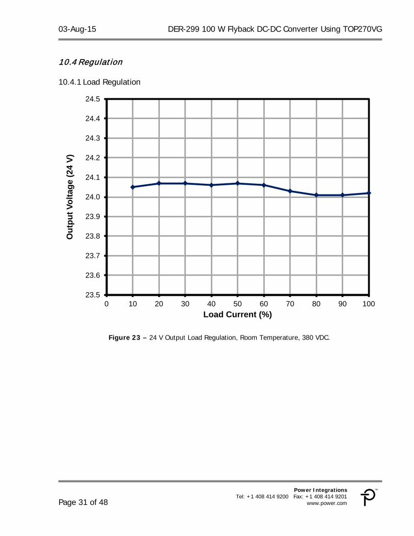
10.4 Regulation
10.4.1 Load Regulation
23.5
23.6
23.7
23.8
23.9
24.0
24.1
24.2
24.3
24.4
24.5
0 10 20 30 40 50 60 70 80 90 100
Out
put V
olta
ge (2
4 V)
Load Current (%)
Figure 23 – 24 V Output Load Regulation, Room Temperature, 380 VDC.

DER-299 100 W Flyback DC-DC Converter Using TOP270VG 03-Aug-15
Page 32 of 48
Power Integrations, Inc. Tel: +1 408 414 9200 Fax: +1 408 414 9201 www.power.com
11.5
11.6
11.7
11.8
11.9
12.0
12.1
12.2
12.3
12.4
12.5
0 10 20 30 40 50 60 70 80 90 100
Out
put V
olta
ge (1
2 V)
Load Current (%)
Figure 24 – 12 V Output Load Regulation, Room Temperature, 380 VDC.
03-Aug-15 DER-299 100 W Flyback DC-DC Converter Using TOP270VG
Page 33 of 48
Power Integrations Tel: +1 408 414 9200 Fax: +1 408 414 9201
www.power.com
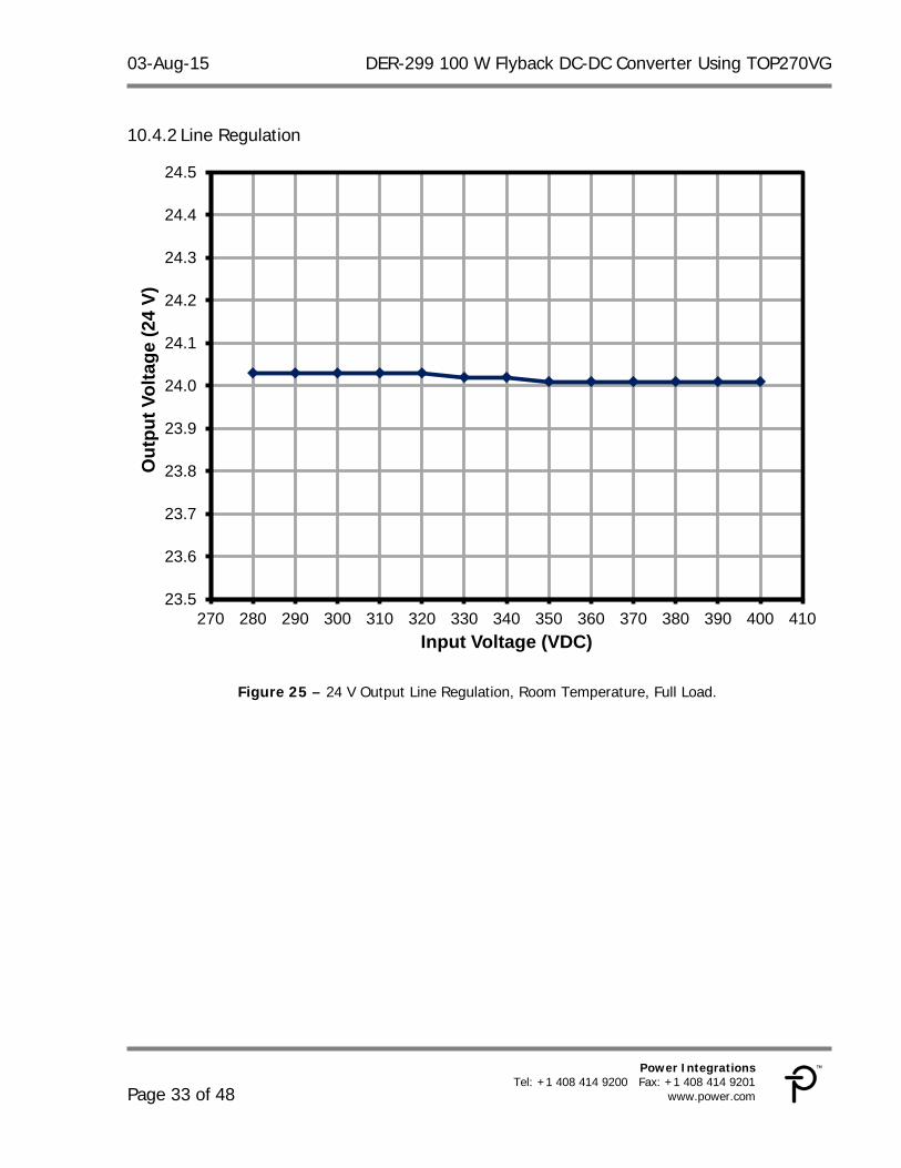
10.4.2 Line Regulation
23.5
23.6
23.7
23.8
23.9
24.0
24.1
24.2
24.3
24.4
24.5
270 280 290 300 310 320 330 340 350 360 370 380 390 400 410
Out
put V
olta
ge (2
4 V)
Input Voltage (VDC)
Figure 25 – 24 V Output Line Regulation, Room Temperature, Full Load.

DER-299 100 W Flyback DC-DC Converter Using TOP270VG 03-Aug-15
Page 34 of 48
Power Integrations, Inc. Tel: +1 408 414 9200 Fax: +1 408 414 9201 www.power.com
11.5
11.6
11.7
11.8
11.9
12.0
12.1
12.2
12.3
12.4
12.5
270 280 290 300 310 320 330 340 350 360 370 380 390 400 410
Out
put V
olta
ge (1
2 V)
Input Voltage (VDC)
Figure 26 – 12 V Output Line Regulation, Room Temperature, Full Load.

03-Aug-15 DER-299 100 W Flyback DC-DC Converter Using TOP270VG
Page 35 of 48
Power Integrations Tel: +1 408 414 9200 Fax: +1 408 414 9201
www.power.com
10.5 Output Cross Regulation To obtain the data shown below, one output was adjusted to maximum load (3 A), while the other was varied between zero load and the maximum load consistent with a maximum total output power of 100 W.
10.5.1 Cross Regulation Data Cross Regulation with 12 V at 3 A Cross Regulation with 24 V at 3 A VOUT IOUT VOUT IOUT VOUT IOUT VOUT IOUT
(24 V) (24 V) (12 V) (12 V) (24 V) (24 V) (12 V) (12 V) 27.12 0.1007 10.81 3.005 23.49 3.008 12.144 0.1008 24.94 0.2508 11.627 3.005 23.77 3.008 12.034 0.2506 24.57 0.5023 11.767 3.005 23.85 3.008 12.001 0.5021 24.34 1.0045 11.855 3.005 23.91 3.008 11.966 1.0086 24.16 2.009 11.873 3.005 24.01 3.008 11.92 2.001 24.12 2.64 11.873 3.005 24.04 3.008 11.905 2.337
DER-299 100 W Flyback DC-DC Converter Using TOP270VG 03-Aug-15
Page 36 of 48
Power Integrations, Inc. Tel: +1 408 414 9200 Fax: +1 408 414 9201 www.power.com
11 Thermal Performance
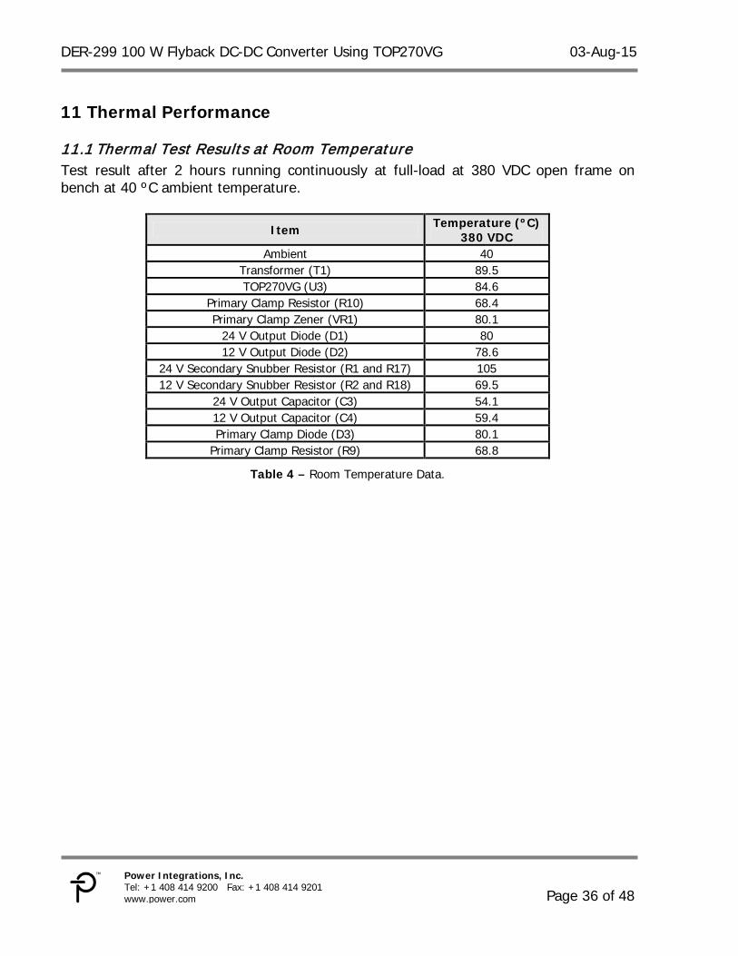
11.1 Thermal Test Results at Room Temperature Test result after 2 hours running continuously at full-load at 380 VDC open frame on bench at 40 ºC ambient temperature.
Item Temperature (ºC) 380 VDC
Ambient 40 Transformer (T1) 89.5 TOP270VG (U3) 84.6
Primary Clamp Resistor (R10) 68.4 Primary Clamp Zener (VR1) 80.1
24 V Output Diode (D1) 80 12 V Output Diode (D2) 78.6
24 V Secondary Snubber Resistor (R1 and R17) 105 12 V Secondary Snubber Resistor (R2 and R18) 69.5
24 V Output Capacitor (C3) 54.1 12 V Output Capacitor (C4) 59.4 Primary Clamp Diode (D3) 80.1
Primary Clamp Resistor (R9) 68.8
Table 4 – Room Temperature Data.

03-Aug-15 DER-299 100 W Flyback DC-DC Converter Using TOP270VG
Page 37 of 48
Power Integrations Tel: +1 408 414 9200 Fax: +1 408 414 9201
www.power.com
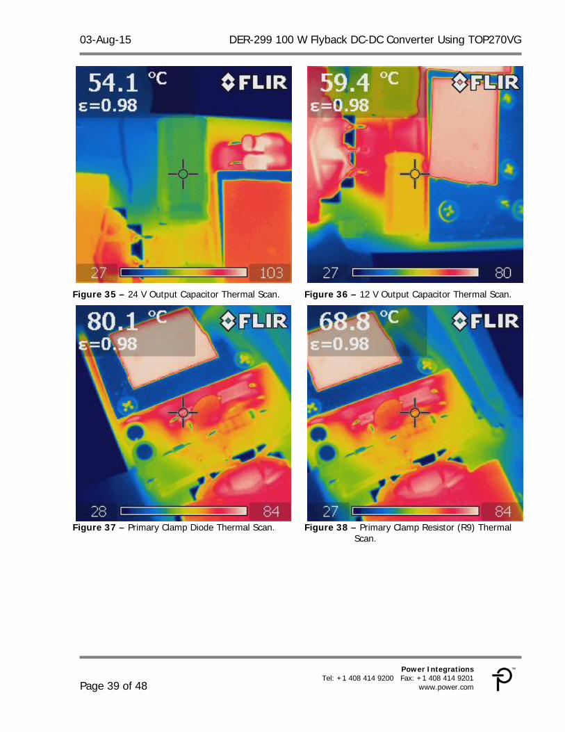
11.2 Thermal Scan at Room Temperature
Figure 27 – Transformer Thermal Scan.
Figure 28 – TOP270VG Thermal Scan.
Figure 29 – Primary Clamp Resistor (R10) Thermal
Scan.
Figure 30 – Primary Clamp Zener Thermal Scan.

DER-299 100 W Flyback DC-DC Converter Using TOP270VG 03-Aug-15
Page 38 of 48
Power Integrations, Inc. Tel: +1 408 414 9200 Fax: +1 408 414 9201 www.power.com
Figure 31 – 24 V Output Diode Thermal Scan.
Figure 32 – 12 V Output Diode Thermal Scan.
Figure 33 – 24 V Sec. Snubber Resistor Thermal
Scan.
Figure 34 – 12 V Sec. Snubber Resistor Thermal
Scan.
03-Aug-15 DER-299 100 W Flyback DC-DC Converter Using TOP270VG
Page 39 of 48
Power Integrations Tel: +1 408 414 9200 Fax: +1 408 414 9201
www.power.com
Figure 35 – 24 V Output Capacitor Thermal Scan.
Figure 36 – 12 V Output Capacitor Thermal Scan.
Figure 37 – Primary Clamp Diode Thermal Scan.
Figure 38 – Primary Clamp Resistor (R9) Thermal
Scan.
DER-299 100 W Flyback DC-DC Converter Using TOP270VG 03-Aug-15
Page 40 of 48
Power Integrations, Inc. Tel: +1 408 414 9200 Fax: +1 408 414 9201 www.power.com
12 Waveforms
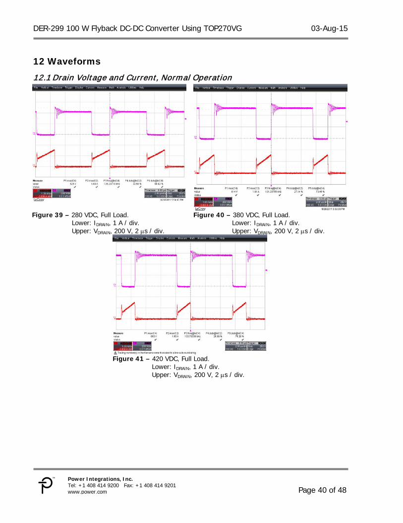
12.1 Drain Voltage and Current, Normal Operation
Figure 39 – 280 VDC, Full Load. Lower: IDRAIN, 1 A / div. Upper: VDRAIN, 200 V, 2 µs / div.
Figure 40 – 380 VDC, Full Load. Lower: IDRAIN, 1 A / div. Upper: VDRAIN, 200 V, 2 µs / div.
Figure 41 – 420 VDC, Full Load.
Lower: IDRAIN, 1 A / div. Upper: VDRAIN, 200 V, 2 µs / div.
03-Aug-15 DER-299 100 W Flyback DC-DC Converter Using TOP270VG
Page 41 of 48
Power Integrations Tel: +1 408 414 9200 Fax: +1 408 414 9201
www.power.com
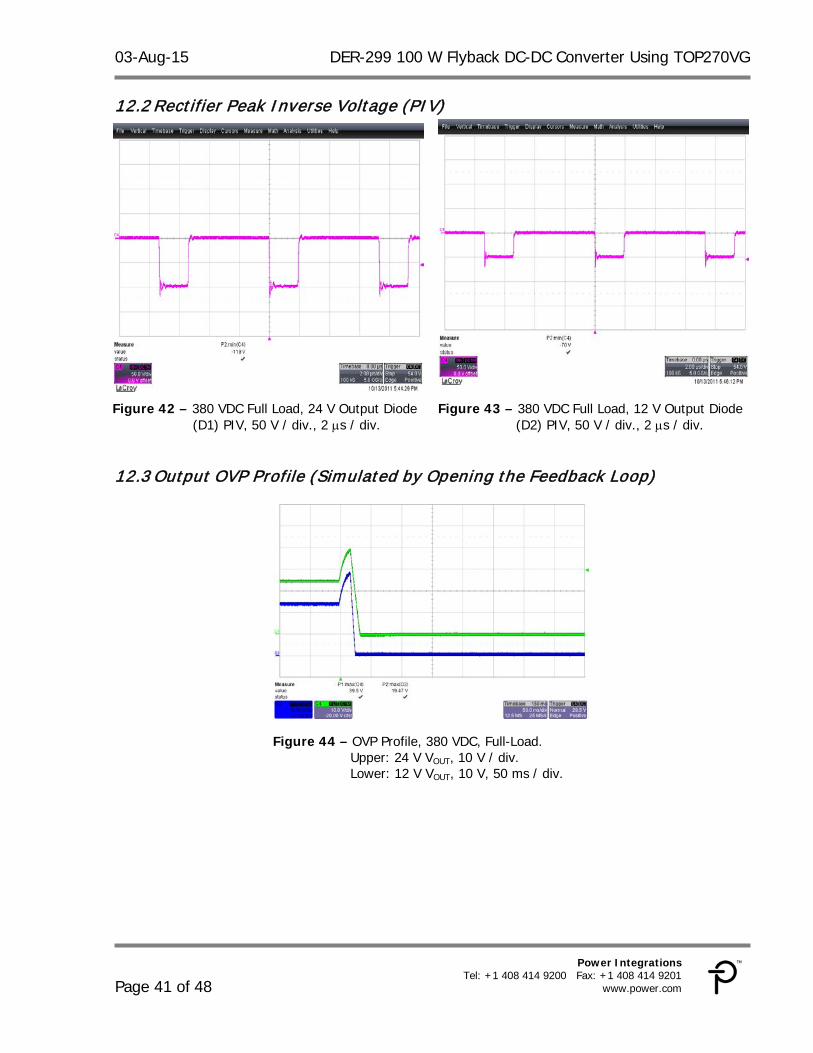
12.2 Rectifier Peak Inverse Voltage (PIV)
Figure 42 – 380 VDC Full Load, 24 V Output Diode (D1) PIV, 50 V / div., 2 µs / div.
Figure 43 – 380 VDC Full Load, 12 V Output Diode (D2) PIV, 50 V / div., 2 µs / div.
12.3 Output OVP Profile (Simulated by Opening the Feedback Loop)
Figure 44 – OVP Profile, 380 VDC, Full-Load. Upper: 24 V VOUT, 10 V / div. Lower: 12 V VOUT, 10 V, 50 ms / div.

DER-299 100 W Flyback DC-DC Converter Using TOP270VG 03-Aug-15
Page 42 of 48
Power Integrations, Inc. Tel: +1 408 414 9200 Fax: +1 408 414 9201 www.power.com
12.4 OCP Profile
Figure 45 – OCP Profile, Short-Circuit on 24 V,
380 VDC. Upper (Red): 24 VOUT Load Current, 5 A / div. Middle (Pink): 24 VOUT, 5 V / div. Lower (Sky Blue): 12 VOUT, 5 V / div, 500 ms / div.
Figure 46 – OCP Profile, Short-Circuit on 12 V, 380 VDC. Upper (Red): 24 VOUT Load Current, 10 A / div. Middle (Pink): 24 VOUT, 5 V / div. Lower (Sky Blue): 12 VOUT, 5 V / div, 500 ms / div.
12.5 Output Voltage Start-up Profile (Constant Resistance Mode)
Figure 47 – Output Voltage Start-up Profile, 380 VDC, No-Load. Upper: 24 V VOUT, 5 V / div. Lower: 12 V VOUT, 5 V, 20 ms / div.
Figure 48 – Output Voltage Start-up Profile, 380 VDC, Full-Load. Upper: 24 V VOUT, 5 V / div. Lower: 12 V VOUT, 5 V, 20 ms / div.

03-Aug-15 DER-299 100 W Flyback DC-DC Converter Using TOP270VG
Page 43 of 48
Power Integrations Tel: +1 408 414 9200 Fax: +1 408 414 9201
www.power.com
12.6 Load Transient Response (50% to 100% Load Step) In the figures shown below, signal averaging was used to better enable viewing the load transient response. The oscilloscope was triggered using the load current step as a trigger source. Since the output switching and line frequency occur essentially at random with respect to the load transient, contributions to the output ripple from these sources will average out, leaving the contribution only from the load step response.
Figure 49 – 50%-100% Load Transient on 24 VOUT 100% Load on 12 VOUT. Upper: 24 VOUT Load Current, 1 A / div. Middle: 24 VOUT AC Coupled, 200 mV / div. Lower: 12 VOUT AC Coupled, 200 mV / div, 100 ms / div.
Figure 50 – 50%-100% Load Transient on 12 VOUT 100% Load on 24 VOUT. Upper: 24 VOUT Load Current, 1 A / div. Middle: 24 VOUT AC Coupled, 200 mV / div. Lower: 12 VOUT AC Coupled, 200 mV / div, 100 ms/ div.

DER-299 100 W Flyback DC-DC Converter Using TOP270VG 03-Aug-15
Page 44 of 48
Power Integrations, Inc. Tel: +1 408 414 9200 Fax: +1 408 414 9201 www.power.com
12.7 Output Ripple Measurements
12.7.1 Ripple Measurement Technique For DC output ripple measurements, a modified oscilloscope test probe must be utilized in order to reduce spurious signals due to pick up. Details of the probe modification are provided in the Figures below. The 4987BA probe adapter is affixed with two capacitors tied in parallel across the probe tip. The capacitors include one (1) 0.1 µF / 50 V ceramic type and one (1) 1.0 µF / 50 V aluminum electrolytic. The aluminum electrolytic type capacitor is polarized, so proper polarity across DC outputs must be maintained (see below).
Figure 51 – Oscilloscope Probe Prepared for Ripple Measurement. (End Cap and Ground Lead Removed.)
Figure 52 – Oscilloscope Probe with Probe Master (www.probemaster.com) 4987A BNC Adapter.
(Modified with wires for ripple measurement, and two parallel decoupling capacitors added.)
Probe Ground
Probe Tip
03-Aug-15 DER-299 100 W Flyback DC-DC Converter Using TOP270VG
Page 45 of 48
Power Integrations Tel: +1 408 414 9200 Fax: +1 408 414 9201
www.power.com
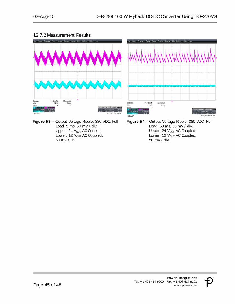
12.7.2 Measurement Results
Figure 53 – Output Voltage Ripple, 380 VDC, Full
Load. 5 ms, 50 mV / div. Upper: 24 VOUT AC Coupled Lower: 12 VOUT AC Coupled, 50 mV / div.
Figure 54 – Output Voltage Ripple, 380 VDC, No-Load. 50 ms, 50 mV / div. Upper: 24 VOUT AC Coupled Lower: 12 VOUT AC Coupled, 50 mV / div.

DER-299 100 W Flyback DC-DC Converter Using TOP270VG 03-Aug-15
Page 46 of 48
Power Integrations, Inc. Tel: +1 408 414 9200 Fax: +1 408 414 9201 www.power.com
13 Control Loop Measurements EQUIPMENT: Frequency Response Analyzer Model 5060A VENABLE
13.1 380 VDC Input Maximum Load
Figure 55 – Gain-Phase Plot, Maximum Steady-State Load.
Vertical Scale: Gain = 10 dB / div., Phase = 30° / div. 380 VDC Input – Crossover Frequency = 1.9 kHz Phase Margin = 70°.

03-Aug-15 DER-299 100 W Flyback DC-DC Converter Using TOP270VG
Page 47 of 48
Power Integrations Tel: +1 408 414 9200 Fax: +1 408 414 9201
www.power.com
14 Revision History Date Author Revision Description and Changes Reviewed
19-Mar-12 SS 1.2 Initial Release Apps & Mktg 27-Mar-12 KM 1.3 Added Control Loop Measurements 03-Aug-15 KM 1.4 Updated VR2, Figure 44 and Brand
Style

DER-299 100 W Flyback DC-DC Converter Using TOP270VG 03-Aug-15
Page 48 of 48
Power Integrations, Inc. Tel: +1 408 414 9200 Fax: +1 408 414 9201 www.power.com
For the latest updates, visit our website: www.power.com Power Integrations reserves the right to make changes to its products at any time to improve reliability or manufacturability. Power Integrations does not assume any liability arising from the use of any device or circuit described herein. POWER INTEGRATIONS MAKES NO WARRANTY HEREIN AND SPECIFICALLY DISCLAIMS ALL WARRANTIES INCLUDING, WITHOUT LIMITATION, THE IMPLIED WARRANTIES OF MERCHANTABILITY, FITNESS FOR A PARTICULAR PURPOSE, AND NON-INFRINGEMENT OF THIRD PARTY RIGHTS.
PATENT INFORMATION The products and applications illustrated herein (including transformer construction and circuits’ external to the products) may be covered by one or more U.S. and foreign patents, or potentially by pending U.S. and foreign patent applications assigned to Power Integrations. A complete list of Power Integrations’ patents may be found at www.power.com. Power Integrations grants its customers a license under certain patent rights as set forth at http://www.power.com/ip.htm. The PI Logo, TOPSwitch, TinySwitch, LinkSwitch, LYTSwitch, InnoSwitch, DPA-Switch, PeakSwitch, CAPZero, SENZero, LinkZero, HiperPFS, HiperTFS, HiperLCS, Qspeed, EcoSmart, Clampless, E-Shield, Filterfuse, FluxLink, StackFET, PI Expert and PI FACTS are trademarks of Power Integrations, Inc. Other trademarks are property of their respective companies. ©Copyright 2015 Power Integrations, Inc. Power Integrations Worldwide Sales Support Locations
WORLD HEADQUARTERS 5245 Hellyer Avenue San Jose, CA 95138, USA. Main: +1-408-414-9200 Customer Service: Phone: +1-408-414-9665 Fax: +1-408-414-9765 e-mail: [email protected]
GERMANY Lindwurmstrasse 114 80337, Munich Germany Phone: +49-895-527-39110 Fax: +49-895-527-39200 e-mail: [email protected]
JAPAN Kosei Dai-3 Building 2-12-11, Shin-Yokohama, Kohoku-ku, Yokohama-shi, Kanagawa 222-0033 Japan Phone: +81-45-471-1021 Fax: +81-45-471-3717 e-mail: [email protected]
TAIWAN 5F, No. 318, Nei Hu Rd., Sec. 1 Nei Hu District Taipei 11493, Taiwan R.O.C. Phone: +886-2-2659-4570 Fax: +886-2-2659-4550 e-mail: [email protected]
CHINA (SHANGHAI) Rm 2410, Charity Plaza, No. 88, North Caoxi Road, Shanghai, PRC 200030 Phone: +86-21-6354-6323 Fax: +86-21-6354-6325 e-mail: [email protected]
INDIA #1, 14th Main Road Vasanthanagar Bangalore-560052 India Phone: +91-80-4113-8020 Fax: +91-80-4113-8023 e-mail: [email protected]
KOREA RM 602, 6FL Korea City Air Terminal B/D, 159-6 Samsung-Dong, Kangnam-Gu, Seoul, 135-728 Korea Phone: +82-2-2016-6610 Fax: +82-2-2016-6630 e-mail: [email protected]
UK Cambridge Semiconductor, a Power Integrations company Westbrook Centre, Block 5, 2nd Floor Milton Road Cambridge CB4 1YG Phone: +44 (0) 1223-446483
e-mail: [email protected]
CHINA (SHENZHEN) 17/F, Hivac Building, No. 2, Keji Nan 8th Road, Nanshan District, Shenzhen, China, 518057 Phone: +86-755-8672-8689 Fax: +86-755-8672-8690 e-mail: [email protected]
ITALY Via Milanese 20, 3rd. Fl. 20099 Sesto San Giovanni (MI) Italy Phone: +39-024-550-8701 Fax: +39-028-928-6009 e-mail: [email protected]
SINGAPORE 51 Newton Road, #19-01/05 Goldhill Plaza Singapore, 308900 Phone: +65-6358-2160 Fax: +65-6358-2015 e-mail: [email protected]