design example report · 4.1 input emi filtering and rectifier ..... 8 4.2 pfs729eg boost converter...
TRANSCRIPT

Power Integrations
5245 Hellyer Avenue, San Jose, CA 95138 USA. Tel: +1 408 414 9200 Fax: +1 408 414 9201
www.powerint.com
Design Example Report
Title 900 W PFC Stage Using HiperPFSTM
PFS729EG
Specification 180 VAC – 264 VAC Input; 380 VDC Output
Application PFC Front End Stage
Author Application Engineering Department
Document Number
DER-274
Date May 12, 2011
Revision 1.0 Summary and Features
Low component count, high performance PFC EN61000-3-2 Class-D compliance with low component count High PFC efficiency enables 80 Plus PC Main design Frequency sliding maintains high efficiency across load range Feed forward line sense gain – maintains relatively constant loop gain over entire
operating voltage range Excellent transient load response Power Integration eSIP™ low-profile package
PATENT INFORMATION The products and applications illustrated herein (including transformer construction and circuits external to the products) may be covered by one or more U.S. and foreign patents, or potentially by pending U.S. and foreign patent applications assigned to Power Integrations. A complete list of Power Integrations' patents may be found at www.powerint.com. Power Integrations grants its customers a license under certain patent rights as set forth at <http://www.powerint.com/ip.htm>. .

DER-274 900 W PFC Using PFS729EG 12-May-11
Page 2 of 48
Power Integrations, Inc. Tel: +1 408 414 9200 Fax: +1 408 414 9201 www.powerint.com
Table of Contents 1 Introduction ................................................................................................................. 4 2 Power Supply Specification ........................................................................................ 6 3 Schematic ................................................................................................................... 7 4 Circuit Description ...................................................................................................... 8
4.1 Input EMI Filtering and Rectifier .......................................................................... 8 4.2 PFS729EG Boost Converter ............................................................................... 8 4.3 Bias Supply Regulator ......................................................................................... 8 4.4 Input Feed Forward Sense Circuit ....................................................................... 8 4.5 Output Feedback ................................................................................................. 9
5 PCB Layout .............................................................................................................. 10 6 Heat Sink Drawing .................................................................................................... 11 7 Bill of Materials ......................................................................................................... 12 8 Inductor Design Spreadsheet ................................................................................... 15 9 Inductor Specification ............................................................................................... 19
9.1 Electrical Diagram ............................................................................................. 19 9.2 Electrical Specifications ..................................................................................... 19 9.3 Materials: ........................................................................................................... 19 9.4 Inductor Winding Instruction .............................................................................. 20
10 Performance Data ................................................................................................. 23 10.1 Efficiency (with RT1 shorted) ............................................................................. 23 10.2 Input Power Factor ............................................................................................ 24 10.3 Regulation ......................................................................................................... 25
10.3.1 Load ........................................................................................................... 25 10.3.2 Line ............................................................................................................ 26
10.4 Input Current Harmonic Distortion (IEC 61000-3-2 Class-D) ............................. 27 10.4.1 50% Load at Output ................................................................................... 27 10.4.2 100% Load at Output ................................................................................. 28
11 Thermal Performance ........................................................................................... 29 12 Waveforms ............................................................................................................ 30
12.1 Input Current at 230 VAC and 50 Hz ................................................................. 30 12.2 Start-up at 180 VAC and 50 Hz ......................................................................... 31 12.3 Start-up at 230 VAC and 50 Hz ......................................................................... 31 12.4 Start-up at 264 VAC and 50 Hz ......................................................................... 32 12.5 Load Transient Response (180 VAC, 50 Hz) .................................................... 33 12.6 Load Transient Response (230 VAC, 50 Hz) .................................................... 34 12.7 Load Transient Response (264 VAC, 50 Hz) .................................................... 34 12.8 1000 ms Line Dropout (230 VAC / 50 Hz) ......................................................... 35 12.9 One Cycle Line Dropout (230 VAC / 50 Hz 0 Degree and 90 Degree) .............. 35 12.10 Line Sag (230 VAC – 180 VAC – 230 VAC, 50 Hz) ....................................... 36 12.11 Line Surge (264 VAC – 293 VAC – 264 VAC, 50 Hz) .................................... 36 12.12 Brown-In and Brown-Out at 6 V / Minute Rate ............................................... 37 12.13 Drain Voltage and Current ............................................................................. 38
12.13.1 Drain Voltage and Current at 230 VAC Input and Full Load ................... 38 12.14 Output Ripple Measurements ........................................................................ 39

12-May-11 DER-274 900 W PFC Using PFS729EG
Page 3 of 48
Power Integrations Tel: +1 408 414 9200 Fax: +1 408 414 9201
www.powerint.com
12.14.1 Ripple Measurement Technique ............................................................. 39 12.14.2 Measurement Results ............................................................................. 40
13 Control Loop Measurements ................................................................................. 42 14 Line Surge ............................................................................................................. 44 15 EMI Scans ............................................................................................................. 45
15.1 EMI Test Set-up ................................................................................................. 45 15.2 EMI Scans ......................................................................................................... 46
16 Revision History .................................................................................................... 47 Important Note: Although this board is designed to satisfy safety isolation requirements, the engineering prototype has not been agency approved. Therefore, all testing should be performed using an isolation transformer to provide the AC input to the prototype board.
DER-274 900 W PFC Using PFS729EG 12-May-11
Page 4 of 48
Power Integrations, Inc. Tel: +1 408 414 9200 Fax: +1 408 414 9201 www.powerint.com
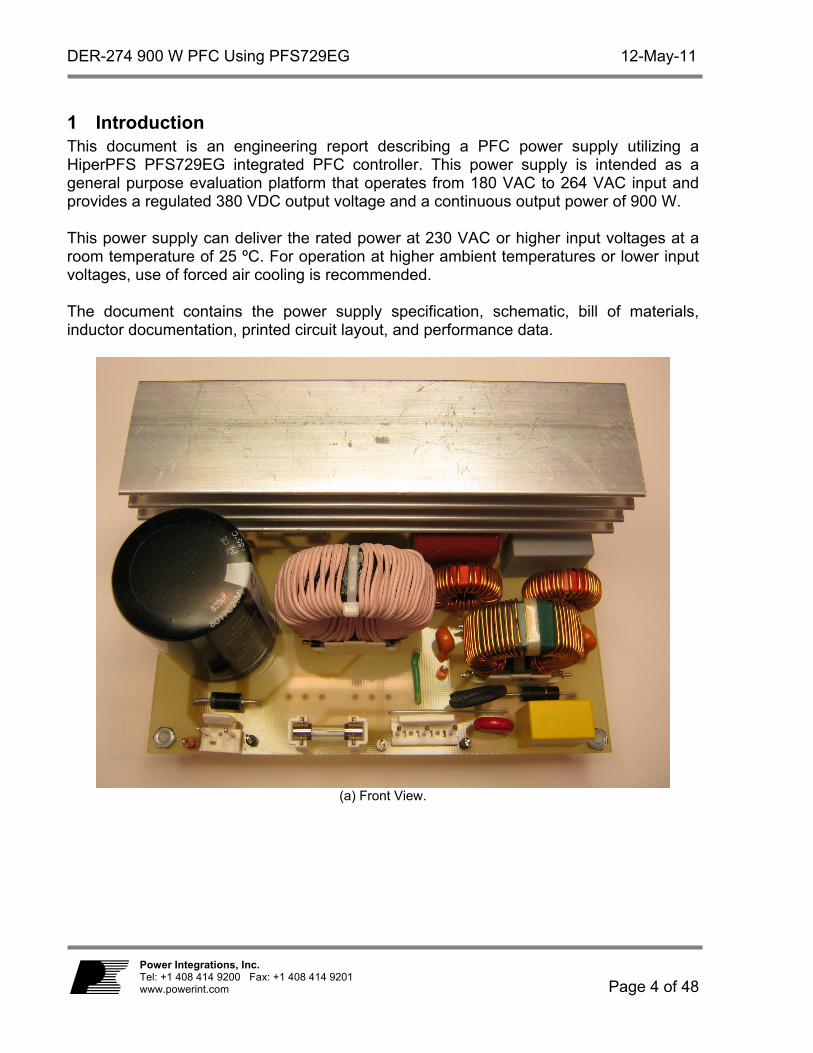
1 Introduction This document is an engineering report describing a PFC power supply utilizing a HiperPFS PFS729EG integrated PFC controller. This power supply is intended as a general purpose evaluation platform that operates from 180 VAC to 264 VAC input and provides a regulated 380 VDC output voltage and a continuous output power of 900 W. This power supply can deliver the rated power at 230 VAC or higher input voltages at a room temperature of 25 ºC. For operation at higher ambient temperatures or lower input voltages, use of forced air cooling is recommended. The document contains the power supply specification, schematic, bill of materials, inductor documentation, printed circuit layout, and performance data.
(a) Front View.

12-May-11 DER-274 900 W PFC Using PFS729EG
Page 5 of 48
Power Integrations Tel: +1 408 414 9200 Fax: +1 408 414 9201
www.powerint.com
(b) Back View.
(c) Bottom View.
Figure 1 – Populated Circuit Board Photograph. (a) Front View; (b) Back View; (c) Bottom View.

DER-274 900 W PFC Using PFS729EG 12-May-11
Page 6 of 48
Power Integrations, Inc. Tel: +1 408 414 9200 Fax: +1 408 414 9201 www.powerint.com
2 Power Supply Specification The table below represents the minimum acceptable performance of the design. Actual performance is listed in the results section.
Description Symbol Min Typ Max Units Comment
Input Voltage VIN 180 264 VAC 3 Wire
Frequency fLINE 47 50 64 Hz
Output
Output Voltage VOUT 370 380 390 V
Output Ripple Voltage p-p VRIPPLE 30 V 20 MHz bandwidth
Output Current IOUT 2.3 A
Total Output Power
Continuous Output Power POUT 900 W
Efficiency
Full Load 97 % Measured at POUT 25 oC
Minimum efficiency at 20, 50 and 100 % of POUT 80+ 97 % Measured at 230 VAC Input
Environmental
Line Surge Differential Mode (L1-L2) Common mode (L1/L2-PE)
1 2
kV kV
1.2/50 s surge, IEC 1000-4-5, Series Impedance:
Differential Mode: 2 Common Mode: 12
Ambient Temperature TAMB 0 50 oC Forced convection required at TAMB
> 25 ºC and/or VIN < 230 V, sea level
Auxiliary Supply Input
Auxiliary Supply VAUX 15 24 V DC Supply

12-May-11 DER-274 900 W PFC Using PFS729EG
Page 7 of 48
Power Integrations Tel: +1 408 414 9200 Fax: +1 408 414 9201
www.powerint.com
3 Schematic
Figure 2 – Schematic.

DER-274 900 W PFC Using PFS729EG 12-May-11
Page 8 of 48
Power Integrations, Inc. Tel: +1 408 414 9200 Fax: +1 408 414 9201 www.powerint.com
4 Circuit Description This PFC circuit is designed using Power Integration’s HiperPFS PFS729EG integrated PFC controller. This design is rated for a continuous output power of 900 W and provides a regulated output voltage of 380 VDC nominal maintaining a high input power factor and overall efficiency from light load to full load.
4.1 Input EMI Filtering and Rectifier Fuse F1 provides protection to the circuit and isolates it from the AC supply in case of a fault. Diode bridge BR1 rectifies the AC input. Capacitors C1, C2, C3, and C4 together with inductors L1, L2 and L3 form the EMI filter reducing the common mode and differential mode noise. Resistors R1, R2 and CAPZero, IC U1 are required to discharge the EMI filter capacitors once the circuit is disconnected. High frequency decoupling capacitor C5 after the bridge reduces the loop area of the high frequency loop and helps reduce the noise coupled into the input wires. Resistor R3 connected in series with capacitor C1 provides damping. Metal Oxide Varistor RV1 is placed across AC power lines to provide differential mode surge protection.
4.2 PFS729EG Boost Converter The boost converter stage consists of inductor L4, diode rectifier D2 and the PFS729EG IC U2. This converter stage works as a variable frequency continuous conduction mode boost converter and controls the input current of the power supply while simultaneously regulating the output DC voltage. Diode D1 prevents a resonant buildup of output voltage at start-up by bypassing inductor L4 while simultaneously charging output capacitor C13. Thermistor RT1 limits the inrush current of the circuit at start-up. In higher performance (efficiency) power supplies, this thermistor is shorted after start-up using a relay. Efficiency measurements should therefore be taken with RT1 shorted to obtain maximum efficiency data. Capacitors C11 and C12 are used for reducing the loop length and area of the output circuit to reduce EMI and overshoot of the voltage across the drain and source of the MOSFET inside U2 at each switching instant.
4.3 Bias Supply Regulator The PFS729EG IC requires a regulated supply of 12 V for operation. Should this supply exceed 13.4 V, the IC could be damaged. Resistors R7, R8, R9, Zener diode VR1, and transistor Q1 form a shunt regulator that prevents the supply voltage to IC U2 from exceeding 12 V. Capacitors C6, C7 and C8 filter the supply voltage to ensure reliable operation of IC U2. Diode D3 protects the circuit against accidental reversal of polarity of the bias supply.
4.4 Input Feed Forward Sense Circuit The input voltage of the power supply is sensed by the IC U2 using resistors R4, R5 and R6. The capacitor C9 filters any noise on this signal.

12-May-11 DER-274 900 W PFC Using PFS729EG
Page 9 of 48
Power Integrations Tel: +1 408 414 9200 Fax: +1 408 414 9201
www.powerint.com
4.5 Output Feedback Divider network comprising of resistors R12, R13, R14, R16, R17 and R18 are used to scale the output voltage and provide a feedback to the IC U2. Capacitor C14 provides soft-finish to prevent output voltage overshoot at start-up. Capacitor C16 filters out any noise coupled into the feedback divider network. The circuit comprising of diode D4, transistor Q2, Q3 and the resistors R16 and R17 forms a non-linear feedback circuit which improves the transient (load) response by improving the response time of the PFC circuit, under large signal condition (e.g. full to no-load step). Resistor R10, R11, R15 and capacitors C15 and C10 are required for shaping the loop response of the feedback circuit. The combination of resistor R11 and capacitor C15 provide a low frequency zero. Diode D5 protects against the single point fault condition of C15 short-circuited. Diode D5 ensures that during this single-fault condition, the FEEDBACK pin of IC U2 is pulled below the FBOFF threshold, thereby, protecting the circuit by inhibiting switching.
Want More?Use your smartphone and free software from www.neoreader.com (or any other free QR Code Reader from your smartphone’s App Store) and you will be connected to related content

DER-274 900 W PFC Using PFS729EG 12-May-11
Page 10 of 48
Power Integrations, Inc. Tel: +1 408 414 9200 Fax: +1 408 414 9201 www.powerint.com
5 PCB Layout
Figure 3 – Printed Circuit Layout (4” x 5.5”).
Figure 4 – Zoomed Portion of Printed Circuit Layout Showing HiperPFS.

12-May-11 DER-274 900 W PFC Using PFS729EG
Page 11 of 48
Power Integrations Tel: +1 408 414 9200 Fax: +1 408 414 9201
www.powerint.com
6 Heat Sink Drawing
Figure 5 – Heat Sink Drawing.

DER-274 900 W PFC Using PFS729EG 12-May-11
Page 12 of 48
Power Integrations, Inc. Tel: +1 408 414 9200 Fax: +1 408 414 9201 www.powerint.com
7 Bill of Materials Item Qty Ref Des Description Mfg Part Number Mfg
1 1 BR1 600 V, 10 A, Bridge Rectifier, GBJ Package
GBJ1006-BP Micro Commercial
2 1 C1 680 nF, 275 VAC, Film, MPX Series, X2 PX684K3ID6 Carli
3 2 C2 C3 220 pF, Ceramic Y1 440LT33-R Vishay
4 1 C4 1 F, 310 VAC, Polyester Film, X2 BFC233820105 BC components
5 1 C5 1.5 F, 400 V, Polypropylene Film ECW-F4155JB Panasonic
6 1 C6 47 F, 50 V, Electrolytic, (6.3 x 11) EKMG500ELL470MF11D Nippon Chemi-Con
7 1 C7 100 nF, 50 V, Ceramic, X7R, 0805 C2012X7R1H104K TDK
8 1 C8 1 F, 25 V, Ceramic, X7R, 1206 C3216X7R1E105K TDK
9 1 C9 47 nF, 50 V, Ceramic, X7R, 0805 ECJ-2YB1H473K Panasonic
10 1 C10 10 nF, 50 V, Ceramic, X7R, 0805 ECJ-2VB1H103K Panasonic
11 2 C11 C12 10 nF, 1 kV, Disc Ceramic, X7R SV01AC103KAR AVX
12 1 C13 820 F, 420 V, Electrolytic, TS-UQ, (35 x 30)
EET-UQ2S821LA Panasonic
13 1 C14 100 nF, 200 V, Ceramic, X7R, 1812 18122C104KAT2A AVX
14 1 C15 4.7 F, 25 V, Ceramic, X7R, 1206 ECJ-3YB1E475M Panasonic
15 1 C16 470 pF, 100 V, Ceramic, X7R, 0805 08051C471KAT2A AVX
16 1 D1 1000 V, 3 A, Recitifier, DO-201AD 1N5408-T Diodes, Inc.
17 1 D2 600 V, 12 A, Ultrafast Recovery, 45 ns, TO-220AC
STTH12R06D ST Semi
18 1 D3 50 V, 1 A, Rectifier, Glass Passivated, DO-213AA (MELF)
DL4001-13-F Diodes, Inc
19 1 D4 75 V, 300 mA, Fast Switching, DO-35 1N4148TR Vishay
20 1 D5 130 V, 5%, 250 mW, SOD-123 BAV116W-7-F Diodes Inc
21 1 ESIPCLIP
M4 METAL1
Heat sink Hardware, Edge Clip, 20.76 mm L x 8 mm W x 0.015 mm Thk
NP975864 Aavid Thermalloy
22 1 F1 8 A, 250 V, Fast, 5 mm x 20 mm, Cartridge
0217008.HXP Littelfuse
23 1 FH1 Fuse Holder Open 5 X 20 mm PC MNT 64900001039 Wickmann
24 1 HS1 Heat sink ,Custom, Al AAVID
25 1 HSPREADER_ESIPP
FISW1
Heat Spreader, Custom, Al, 3003, 0.030 in Thk
61-00040-00 Custom
26 1 J1 5 Position (1 x 5) header, 0.156 pitch, Vertical
26-64-4050 Molex
27 1 J2 CONN header 3 Position (1x3).156 Vertical TIN
26-64-4030 Molex
28 1 J3 2 Position (1 x 2) header, 0.1 pitch, Vertical
22-23-2021 Molex
29 2 JP1 JP4 Wire Jumper, Insulated, TFE, #22 AWG, 0.5 in
C2004-12-02 Alpha
30 3 JP2 JP3
JP5 Wire Jumper, Insulated, TFE, #18 AWG, 0.4 in
C2052A-12-02 Alpha
31 2 JP6 JP7 Wire Jumper, Insulated, TFE, #22 AWG, 0.6 in
C2004-12-02 Alpha

12-May-11 DER-274 900 W PFC Using PFS729EG
Page 13 of 48
Power Integrations Tel: +1 408 414 9200 Fax: +1 408 414 9201
www.powerint.com
32 1 JP8 Wire Jumper, Insulated, TFE, #18 AWG, 1.4 in
C2052A-12-02 Alpha
33 1 L1 8 mH, 5.6 A, Common Mode Choke, 8112-RC JW Miller
34 2 L2 L3 100 H, 5 A, Inductor TORD HI AMP 100 H Vertical
7447070 Wurth
35 1 L4 Custom, 900 W PFC Inductor, 2.04 mH, constructed on Lodestone Pacific base PN VTM160-4
Custom
36 4
POST-CRKT_BR
D_6-32_HEX1
Post, Circuit Board, Female, Hex, 6-32, snap, 0.375L, Nylon
561-0375A Eagle Hardware
37 2 Q1 Q2 NPN, Small Signal BJT, GP SS, 40 V, 0.6 A, SOT-23
MMBT4401T-7-F Diodes, Inc.
38 1 Q3 PNP, Small Signal BJT, 40 V, 0.6 A, SOT-23
MMBT4403-7-F Diodes, Inc.
39 2 R1 R2 220 k, 5%, 1/4 W, Thick Film, 1206 ERJ-8GEYJ224V Panasonic
40 1 R3 2 , 1%, 2 W, Wire Wound WNC2R0FET Ohmite
41 1 R4 3.30 M, 1%, 1/4 W, Thick Film, 1206 KTR18EZPF3304 Rohm Semi
42 1 R5 4.70 M, 1%, 1/4 W, Thick Film, 1206 KTR18EZPF4704 Rohm Semi
43 1 R6 1 M, 1%, 1/4 W, Metal Film MFR-25FBF-1M00 Yageo
44 2 R7 R8 100 , 1%, 1/4 W, Thick Film, 1206 ERJ-8ENF1000V Panasonic
45 2 R9 R11 3.01 k, 1%, 1/4 W, Thick Film, 1206 ERJ-8ENF3011V Panasonic
46 1 R10 2 k, 5%, 1/8 W, Thick Film, 0805 ERJ-6GEYJ202V Panasonic
47 1 R12 1.50 M, 1%, 1/4 W, Thick Film, 1206 ERJ-8ENF1504V Panasonic
48 1 R13 732 k, 1%, 1/4 W, Thick Film, 1206 ERJ-8ENF7323V Panasonic
49 1 R14 1.60 M, 1%, 1/4 W, Thick Film, 1206 ERJ-8ENF1604V Panasonic
50 1 R15 160 k, 5%, 1/8 W, Thick Film, 0805 ERJ-6GEYJ164V Panasonic
51 2 R16 R17 2.21 k, 1%, 1/4 W, Thick Film, 1206 ERJ-8ENF2211V Panasonic
52 1 R18 57.6 k, 1%, 1/4 W, Thick Film, 1206 ERJ-8ENF5762V Panasonic
53 1 RT1 NTC Thermistor, 10 , 5 A CL-60 GE Sensing
54 1 RTV1 Thermally Conductive Silicone Grease 120-SA Wakefield
55 1 RV1 320 V, 23 J, 10 mm, RADIAL V320LA10P Littlefuse
56 3 SCREW1 SCREW2 SCREW3
Screw Machine Phil 4-40 X 3/8 SS PMSSS 440 0038 PH Building Fasteners
57 1 T1 Bobbin, PQ35/35, Vertical, 12 pins BQ35/35-1112CPFR TDK
58 1 TO-220 PAD1
HEATPAD TO-247 .006" K10 K10-104 Bergquist
59 1 TO-220 PAD2
Thermal Pad TO-220 .009" SP1000 1009-58 Bergquist
60 2 TP1 TP4 Test Point, WHT, THRU-HOLE MOUNT 5012 Keystone
61 3 TP2 TP6
TP8 Test Point, BLK, THRU-HOLE MOUNT 5011 Keystone
62 1 TP3 Test Point, ORG, THRU-HOLE MOUNT 5013 Keystone
63 1 TP5 Test Point, YEL, THRU-HOLE MOUNT 5014 Keystone
64 1 TP7 Test Point, RED, THRU-HOLE MOUNT 5010 Keystone

DER-274 900 W PFC Using PFS729EG 12-May-11
Page 14 of 48
Power Integrations, Inc. Tel: +1 408 414 9200 Fax: +1 408 414 9201 www.powerint.com
65 1 U1 CAPZero, SO-8C CAP006DG Power Integrations
66 1 U2 HiperPFS, SIP7/6-TH PFS729EG Power Integrations
67 1 VR1 12 V, 5%, 225 mW, SOT23 BZX84C12LT1G On Semi
68 1 WASHER1 Washer Teflon #6, ID 0.156, OD 0.312, Thk 0.031
FWF-6 See Distributor
69 1 WASHER2 Washer, Shoulder, #4, 0.095 Shoulder x 0.117 Dia, Polyphenylene Sulfide PPS
7721-10PPSG Aavid Thermalloy
70 1 WASHER3 Washer Flat #4 SS FWSS 004 Building Fasteners
71 1 WASHER4 Washer Flat #4 Zinc, OD 0.219, ID 0.125, Thk 0.032,Yellow Chromate Finish
5205820-2 Tyco
72 1 WASHER5 Washer Nylon Shoulder #4 3049 Keystone

12-May-11 DER-274 900 W PFC Using PFS729EG
Page 15 of 48
Power Integrations Tel: +1 408 414 9200 Fax: +1 408 414 9201
www.powerint.com
8 Inductor Design Spreadsheet ACDC_PFS_101210; Rev.1.0; Copyright
Power Integrations 2010 INPUT INFO OUTPUT UNITS
ACDC_HiperPFS_101210_Rev1-0.xls; Continuous Mode Boost Converter Design
Spreadsheet
Enter Applications Variables
Input Voltage Range High_Line High_Line Select Universal or High_Line option
VACMIN 180 V Minimum AC input voltage
VACMAX 264 V Maximum AC input voltage
VBROWNIN 175.01 Expected Minimum Brown-in Voltage
VBROWNOUT 158.46 V Specify brownout voltage.
VO 385 V Nominal Output voltage
PO 900 W Nominal Output power
fL 50 Hz Line frequency
TA Max 40 deg C Maximum ambient temperature
n 0.97 Info 0.97 !!! Info. Efficiency should be between 0.87 and 0.97
KP 0.420 0.42 Ripple to peak inductor current ratio at the peak of VACMIN
VO_MIN 365.75 V Minimum Output voltage
VO_RIPPLE_MAX 20 V Maximum Output voltage ripple
tHOLDUP 20 ms Holdup time
VHOLDUP_MIN 310 V Minimum Voltage Output can drop to during holdup
I_INRUSH 40 A Maximum allowable inrush current
Forced Air Cooling No No Enter "Yes" for Forced air cooling. Otherwise enter "No"
PFS Parameters
PFS Part Number PFS729 PFS729 Selected PFS device
IOCP min 9.30 A Minimum Current limit
IOCP typ 10.30 A Typical current limit
IOCP max 11.30 A Maximum current limit
RDSON 0.40 ohms Typical RDSon at 100 'C
RV 9.00 Mohms Line sense resistor
C_VCC 1.00 uF Supply decoupling capacitor
C_V 47.00 nF V pin decoupling capacitor
C_FB 10.00 nF Feedback pin decoupling capacitor
FS_PK 84.38 kHz Estimated peak frequency of operation
FS_AVG 83.04 kHz Estimated average frequency of operation
IP 9.22 A MOSFET peak current
PFS_IRMS 3.67 A PFS MOSFET RMS current
PCOND_LOSS_PFS 5.38 W Estimated PFS conduction losses
PSW_LOSS_PFS 4.25 W Estimated PFS switching losses
PFS_TOTAL 9.64 W Total Estimated PFS losses
TJ Max 100 deg C Maximum steady-state junction temperature
Rth-JS 3.00 degC/W Maximum thermal resistance (Junction to heatsink)

DER-274 900 W PFC Using PFS729EG 12-May-11
Page 16 of 48
Power Integrations, Inc. Tel: +1 408 414 9200 Fax: +1 408 414 9201 www.powerint.com
HEATSINK Theta-CA 3.22 degC/W Maximum thermal resistance of heatsink
Basic Inductor Calculation
LPFC 237.36 uH Value of PFC inductor at peak of VACMIN and Full Load
LPFC (0 Bias) 2037.31 uH Value of PFC inductor at No load. This is the value measured with LCR meter
LPFC_RMS 5.56 A Inductor RMS current (calculated at VACMIN and Full Load)
Inductor Construction Parameters
Core Type Sendust Sendust Enter "Sendust", "Pow Iron" or "Ferrite"
Core Material Auto 125u
Select from 60u, 75u, 90u or 125 u for Sendust cores. Fixed at PC44 or equivalent for Ferrite cores. Fixed at 52 material for Pow Iron cores.
Core Geometry Auto TOROID Select from Toroid or EE for Sendust cores and from EE, or PQ for Ferrite cores
Core Auto 77254
(OD=40.8) Core part number
AE 107.2 mm^2 Core cross sectional area
LE 98.2 mm Core mean path length
AL 171 nH/t^2 Core AL value
VE 10050 mm^3 Core volume
HT 15.37 mm Core height/Height of window
MLT 54 cm Mean length per turn
BW N/A mm Bobbin width
NL 109 Inductor turns
LG N/A mm Gap length (Ferrite cores only)
ILRMS 5.56 A Inductor RMS current
Wire type LITZ Select between "Litz" or "Regular" for double coated magnet wire
AWG 40 AWG Inductor wire gauge
Filar 250 Inductor wire number of parallel strands
OD 0.079 mm Outer diameter of single strand of wire
AC Resistance Ratio 1.22 Ratio of AC resistance to the DC resistance (using Dowell curves)
J 4.57 A/mm^2 Estimated current density of wires. It is recommended that 4 < J < 6
BM_TARGET N/A Gauss Target flux density at VACMIN (Ferrite cores only)
BM 2582 Gauss Maximum operating flux density
BP 6627 Gauss Peak Flux density (Estimated at VBROWNOUT)
LPFC_CORE_LOSS 2.07 W Estimated Inductor core Loss
LPFC_COPPER_LOSS 2.35 W Estimated Inductor copper losses
LPFC_TOTAL LOSS 4.42 W Total estimated Inductor Losses
Critical Parameters
IRMS 5.15 A AC input RMS current
IO_AVG 2.34 A Output average current
Output Diode
Part Number Auto STTH12R06 PFC Diode Part Number

12-May-11 DER-274 900 W PFC Using PFS729EG
Page 17 of 48
Power Integrations Tel: +1 408 414 9200 Fax: +1 408 414 9201
www.powerint.com
Type ULTRAFAST Diode Type - Special - Diodes specially catered for PFC applications, SiC - Silicon Carbide type, UF - Ultrafast recovery type
Manufacturer ST Diode Manufacturer
VRRM 600 V Diode rated reverse voltage
IF 12 A Diode rated forward current
TRR 25 ns Diode Reverse recovery time
VF 1.1 V Diode rated forward voltage drop
PCOND_DIODE 2.57 W Estimated Diode conduction losses
PSW_DIODE 3.28 W Estimated Diode switching losses
P_DIODE 5.85 W Total estimated Diode losses
TJ Max 125 deg C Maximum Operating temperature
Rth-JS 1.70 degC/W Maximum thermal resistance (Junction to heatsink)
HEATSINK Theta-CA 12.33 degC/W Maximum thermal resistance of heatsink
Output Capacitor
CO Auto 820.00 uF Minimum value of Output capacitance
VO_RIPPLE_EXPECTED 9.4 V Expected ripple voltage on Output with selected Output capacitor
T_HOLDUP_EXPECTED 21.5 ms Expected holdup time with selected Output capacitor
ESR_LF 0.20 ohms
ESR_HF 0.07 ohms
IC_RMS_LF 1.65 A Low Frequency Capacitor RMS current
IC_RMS_HF 2.93 A High Frequency Capacitor RMS current
CO_LF_LOSS 0.55 W Estimated Low Frequency ESR loss in Output capacitor
CO_HF_LOSS 0.61 W Estimated High frequency ESR loss in Output capacitor
Total CO LOSS 1.16 W Total estimated losses in Output Capacitor
Input Bridge and Fuse
I^2t Rating 57.58 A^2s Minimum I^2t rating for fuse
Fuse Current rating 7.26 A Minimum Current rating of fuse
VF 0.90 V Input bridge Diode forward Diode drop
IAVG 4.52 A Input average current at 70 VAC.
PIV_INPUT BRIDGE 375 V Peak inverse voltage of input bridge
PCOND_LOSS_BRIDGE 8.35 W Estimated Bridge Diode conduction loss
CIN 1.00 uF Input capacitor. Use metallized polypropylene or film foil type with high ripple current rating
RT 6.44 ohms Input Thermistor value
D_Precharge 1N5407 Recommended precharge Diode
Feedback Components
R2 1.54 Mohms Feedback network, first high voltage divider resistor
R3 1.54 Mohms Feedback network, second high voltage divider resistor
R4 698.00 kohms Feedback network, third high voltage divider resistor
C2 100.00 nF Feedback network, loop speedup capacitor
R5 2.20 kohms Feedback component, NPN transistor bias resistor

DER-274 900 W PFC Using PFS729EG 12-May-11
Page 18 of 48
Power Integrations, Inc. Tel: +1 408 414 9200 Fax: +1 408 414 9201 www.powerint.com
R6 2.20 kohms Feedback component, PNP transistor bias resistor
R7 57.60 kohms Feedback network, lower divider resistor
C3 470.00 pF Feedback component- noise suppression capacitor
R8 160.00 kohms Feedback network - pole setting resistor
R9 2.67 kohms Feedback network - zero setting resistor
R10 10.00 kohms Feedback pin filter resistor
C4 10.00 uF Feedback network - compensation capacitor
D3 1N4148 Feedback network reverse blocking Diode
D4 1N4001 Feedback network - capacitor failure detection Diode
Q1 2N4401 Feedback network - speedup circuit NPN transistor
Q2 2N4403 Feedback network - speedup circuit PNP transistor
Loss Budget (Estimated at VACMIN)
PFS Losses 9.64 W Total estimated losses in PFS
Boost diode Losses 5.85 W Total estimated losses in Output Diode
Input Bridge losses 8.35 W Total estimated losses in input bridge module
Inductor losses 4.42 W Total estimated losses in PFC choke
Output Capacitor Loss 1.16 W Total estimated losses in Output capacitor
Total losses 29.43 W Overall loss estimate
Efficiency 0.97 Estimated efficiency at VACMIN. Verify efficiency at other line voltages

12-May-11 DER-274 900 W PFC Using PFS729EG
Page 19 of 48
Power Integrations Tel: +1 408 414 9200 Fax: +1 408 414 9201
www.powerint.com
9 Inductor Specification
9.1 Electrical Diagram
Figure 6 – Inductor Electrical Diagram.
9.2 Electrical Specifications Primary Inductance Pins 1-2 measured at 100 kHz, 0.4 VRMS 2.04 mH ±8%
9.3 Materials: Item Description [1] Core: Magnetics Inc, Mfg: 0077254A7 PI P/ N 32-00246-00. [2] Magnet wire: 125/40 Served – Litz wire. [3] Base: Toroid mounting base, Lodestone Pacific, P/N VTM160-4, or similar. See Figure 2.
PI P/N: 76-00004-00. [4] High Temperature Epoxy, Mfg: MG Chemicals, P/N: 832HT-375ML, Digikey: 473-1085-ND,
or similar, PI P/N: 66-00087-00. [5] Divider: Tie-wrap, Panduit, P/N: PLT.7M-M or similar.
Figure 7 – Top View of Toroid Mounting Base Item [3].
109T – 125/40 AWG Served Litzwire
1
2

DER-274 900 W PFC Using PFS729EG 12-May-11
Page 20 of 48
Power Integrations, Inc. Tel: +1 408 414 9200 Fax: +1 408 414 9201 www.powerint.com
9.4 Inductor Winding Instruction Note: Colors used in diagrams used to denote winding layers.
Insert 2 dividers item [5] in the core item [1] to divide into 2 sections equally. See picture below. Take about 15 ft. of wire item [2]. Align center of wire with 1 divider.
Center of wire
Start winding on the left section with 23 turns of wire item [2], for the 1st layer, spread wire evenly and ensure that turns do not overlap.
Wind a further 23 turns on the right section.

12-May-11 DER-274 900 W PFC Using PFS729EG
Page 21 of 48
Power Integrations Tel: +1 408 414 9200 Fax: +1 408 414 9201
www.powerint.com
Continue winding on the right section for the 2nd layer 18 turns, spread wire evenly and ensure that turns do not overlap.
Continue winding on the right section on the 3rd layer 13 turns, spread wire evenly and ensure that turns do not overlap.
Wind the same as above for the 2nd and 3rd layer on the left section. Third layer will have 14 turns
to complete 109 turns total.
Solder the leads to the pin 1 and 2 of mounting base item [3].
Secure the inductor to the base by using high temperature epoxy item [4].

DER-274 900 W PFC Using PFS729EG 12-May-11
Page 22 of 48
Power Integrations, Inc. Tel: +1 408 414 9200 Fax: +1 408 414 9201 www.powerint.com
Front view Back view

12-May-11 DER-274 900 W PFC Using PFS729EG
Page 23 of 48
Power Integrations Tel: +1 408 414 9200 Fax: +1 408 414 9201
www.powerint.com
10 Performance Data All measurements performed at room temperature, 50 Hz input frequency All performance data is with Thermistor’s RT1 shorted to represent the high performance configuration which uses RT1 to limit inrush current and shorts thermistor RT1 after startup to improve operating efficiency.
10.1 Efficiency (with RT1 shorted)
94.5
95.0
95.5
96.0
96.5
97.0
97.5
98.0
98.5
0 100 200 300 400 500 600 700 800 900 1000
Eff
icie
ncy
(%
)
Output Power (W)
180 VAC
230 VAC
264 VAC
Figure 8 – Efficiency vs. Output Power, Room Temperature, 50 Hz.

DER-274 900 W PFC Using PFS729EG 12-May-11
Page 24 of 48
Power Integrations, Inc. Tel: +1 408 414 9200 Fax: +1 408 414 9201 www.powerint.com
10.2 Input Power Factor
0.70
0.75
0.80
0.85
0.90
0.95
1.00
1.05
0 100 200 300 400 500 600 700 800 900 1000
Inp
ut
Po
wer
Fac
tor
(PF
)
Output Power (W)
180 VAC
230 VAC
264 VAC
Figure 9 – Input Power Factor vs. Output Power, Room Temperature; 50 Hz.

12-May-11 DER-274 900 W PFC Using PFS729EG
Page 25 of 48
Power Integrations Tel: +1 408 414 9200 Fax: +1 408 414 9201
www.powerint.com
10.3 Regulation
10.3.1 Load
374
376
378
380
382
384
386
388
390
392
0 100 200 300 400 500 600 700 800 900 1000
Ou
tpu
t V
olt
age
(V)
Output Power (W)
180 VAC
230 VAC
264 VAC
Figure 10 – Load Regulation, Room Temperature.

DER-274 900 W PFC Using PFS729EG 12-May-11
Page 26 of 48
Power Integrations, Inc. Tel: +1 408 414 9200 Fax: +1 408 414 9201 www.powerint.com
10.3.2 Line
374
376
378
380
382
384
386
388
390
392
170 180 190 200 210 220 230 240 250 260 270
Ou
tpu
t V
olt
age
(V)
Input Voltage (VAC)
100% Load
50% Load
10% Load
Figure 11 – Line Regulation, Room Temperature.

12-May-11 DER-274 900 W PFC Using PFS729EG
Page 27 of 48
Power Integrations Tel: +1 408 414 9200 Fax: +1 408 414 9201
www.powerint.com
10.4 Input Current Harmonic Distortion (IEC 61000-3-2 Class-D) Measured at 230 VAC Input 50 Hz
10.4.1 50% Load at Output
0.0
0.5
1.0
1.5
2.0
2.5
3 5 7 9 11 13 15 17 19 21 23 25 27 29 31 33 35 37 39
Am
plit
ud
e (A
)
Harmonic #
Hamonic Limit
Input Current
Figure 12 – Amplitude of Input Current Harmonics for 50% Load at 230 VAC Input.

DER-274 900 W PFC Using PFS729EG 12-May-11
Page 28 of 48
Power Integrations, Inc. Tel: +1 408 414 9200 Fax: +1 408 414 9201 www.powerint.com
10.4.2 100% Load at Output
0.0
0.5
1.0
1.5
2.0
2.5
3 5 7 9 11 13 15 17 19 21 23 25 27 29 31 33 35 37 39
Am
pli
tud
e (A
)
Harmonic #
Hamonic Limit
Input Current
Figure 13 – Amplitude of Input Current Harmonics for 100% Load at 230 VAC Input.

12-May-11 DER-274 900 W PFC Using PFS729EG
Page 29 of 48
Power Integrations Tel: +1 408 414 9200 Fax: +1 408 414 9201
www.powerint.com
11 Thermal Performance The unit was allowed to reach thermal equilibrium prior to the measurement. Table 1 shows full load temperature of key components at equilibrium, room temperature and without any forced air cooling.
Component Temperature (ºC)
230 VAC X1 Capacitor 680 nF, C1 29.3
DC Capacitor after BR 1.5 F, C5 55.4 Output Capacitor 820 F, C13 38.4
X2 Capacitor 1 F, C4 42.4 Output Diode, D2 75.0
CM Inductor 8 mH, L1 58.1 DM Inductor 100 H, L2 53.9 DM Inductor 100 H, L3 66.1
Output Inductor, L4 77.4 Bridge Rectifier, BR1 81.0
eSIP, U2 86.0 Heat Sink (Top Surface) 29.0 Ambient Temperature 24.2
Table 1 – Thermal Performance of Key Components at Full Load.
Figure 14 – Infra-Red Image of the Front and Back Side of the Board at Thermal Equilibrium. 230 VAC,
Full Load, No Forced-Air Flow, 24 ºC Ambient.

DER-274 900 W PFC Using PFS729EG 12-May-11
Page 30 of 48
Power Integrations, Inc. Tel: +1 408 414 9200 Fax: +1 408 414 9201 www.powerint.com
12 Waveforms
12.1 Input Current at 230 VAC and 50 Hz
Figure 15 – 230 VAC, 50% Load. Upper: VIN, 500 V / div. Lower: IIN, 2 A, 10 ms / div.
Figure 16 – 230 VAC, 100% Load. Upper: VIN, 500 V / div. Lower: IIN, 5 A, 10 ms / div.

12-May-11 DER-274 900 W PFC Using PFS729EG
Page 31 of 48
Power Integrations Tel: +1 408 414 9200 Fax: +1 408 414 9201
www.powerint.com
12.2 Start-up at 180 VAC and 50 Hz Load in CC mode during turn-on of PFC
Figure 17 – 180 VAC, No-load. Upper: VIN, 1000 V / div. Second: VOUT, 200 V / div. Third: IIN, 20 A / div. Lower: VCC, 10 V, 50 ms / div.
Figure 18 – 180 VAC, Full Load. Upper: VIN, 1000 V / div. Second: VOUT, 200 V / div. Third: IIN, 20 A / div. Lower: VCC, 10 V, 50 ms / div.
12.3 Start-up at 230 VAC and 50 Hz Load in CC mode during turn-on of PFC
Figure 19 – 230 VAC, No-load. Upper: VIN, 1 kV / div. Second: VOUT, 200 V / div. Third: IIN, 20 A / div. Lower: VCC, 10 V, 50 ms / div.
Figure 20 – 230 VAC, Full Load. Upper: VIN, 1 kV / div. Second: VOUT, 200 V / div. Third: IIN, 20 A / div. Lower: VCC, 10 V, 50 ms / div.

DER-274 900 W PFC Using PFS729EG 12-May-11
Page 32 of 48
Power Integrations, Inc. Tel: +1 408 414 9200 Fax: +1 408 414 9201 www.powerint.com
12.4 Start-up at 264 VAC and 50 Hz Load in CC mode during turn-on of PFC
Figure 21 – 264 VAC, No-load. Upper: VIN, 1 kV / div. Second: VOUT, 200 V / div. Third: IIN, 20 A / div. Lower: VCC, 10 V, 50 ms / div.
Figure 22 – 264 VAC, Full Load. Upper: VIN, 1 kV / div. Second: VOUT, 200 V / div. Third: IIN, 20 A / div Lower: VCC, 10 V, 50 ms / div.

12-May-11 DER-274 900 W PFC Using PFS729EG
Page 33 of 48
Power Integrations Tel: +1 408 414 9200 Fax: +1 408 414 9201
www.powerint.com
12.5 Load Transient Response (180 VAC, 50 Hz) In the figures shown below, signal averaging was used to better enable viewing the load transient response. The oscilloscope was triggered using the load current step as a trigger source. Since the output switching and line frequency occur essentially at random with respect to the load transient, contributions to the output ripple from these sources will average out, leaving the contribution only from the load step response.
Figure 23 – Transient Response, 180 VAC, 10-100-10% Load Step. Upper: VIN, 1 kV / div. Second: IIN, 10 A / div. Third: VOUT (AC Coupled), 50 V / div. Lower: ILOAD 2 A, 100 ms / div.
Figure 24 – Transient Response, 180 VAC, 50-100-50% Load Step Upper: VIN, 1 kV / div. Second: IIN, 10 A / div. Third: VOUT (AC Coupled), 50 V / div. Lower: ILOAD 2 A, 100 ms / div.

DER-274 900 W PFC Using PFS729EG 12-May-11
Page 34 of 48
Power Integrations, Inc. Tel: +1 408 414 9200 Fax: +1 408 414 9201 www.powerint.com
12.6 Load Transient Response (230 VAC, 50 Hz)
Figure 25 – Transient Response, 230 VAC, 10-100-10% Load Step. Upper: VIN, 1 kV / div. Second: IIN, 10 A / div. Third: VOUT (AC Coupled), 50 V / div. Lower: ILOAD 2 A, 100 ms / div.
Figure 26 – Transient Response, 230VAC, 50-100-50% Load Step. Upper: VIN, 1 kV / div. Second: IIN, 10 A / div. Third: VOUT (AC Coupled), 50 V / div. Lower: ILOAD 2 A, 100 ms / div.
12.7 Load Transient Response (264 VAC, 50 Hz)
Figure 27 – Transient Response, 264 VAC, 10-100-10% Load Step. Upper: VIN, 1 kV / div. Second: IIN, 10 A / div. Third: VOUT (AC Coupled), 50 V / div. Lower: ILOAD 2 A, 100 ms / div.
Figure 28 – Transient Response, 264 VAC, 50-100-50% Load Step. Upper: VIN, 1 kV / div. Second: IIN, 10 A / div. Third: VOUT (AC Coupled),50 V / div. Lower: ILOAD 2 A, 100 ms / div.

12-May-11 DER-274 900 W PFC Using PFS729EG
Page 35 of 48
Power Integrations Tel: +1 408 414 9200 Fax: +1 408 414 9201
www.powerint.com
12.8 1000 ms Line Dropout (230 VAC / 50 Hz)
Figure 29 – Line Dropout 230 VAC, 1000 ms. 50% Load. Upper: VIN, 500 V / div. Middle: IIN, 20 A / div. Lower: VOUT, 200 V, 200 ms / div.
Figure 30 – Line Dropout 230 VAC, 1000 ms. 100% Load. Upper: VIN, 500 V / div. Middle: IIN, 20 A / div. Lower: VOUT, 200 V, 200 ms / div.
12.9 One Cycle Line Dropout (230 VAC / 50 Hz 0 Degree and 90 Degree)
Figure 31 – Line Dropout 230 VAC, 50 Hz. 0 Degree. Upper: VIN, 500 V / div. Middle: VOUT, 100 V /div. Lower: IIN, 10 A, 50 ms / div.
Figure 32 – Line Dropout 230 VAC, 50 Hz. 90 Degree. Upper: VIN, 500 V / div. Middle: VOUT, 100 V / div. Lower: IIN, 10 A, 50 ms /div.

DER-274 900 W PFC Using PFS729EG 12-May-11
Page 36 of 48
Power Integrations, Inc. Tel: +1 408 414 9200 Fax: +1 408 414 9201 www.powerint.com
12.10 Line Sag (230 VAC – 180 VAC – 230 VAC, 50 Hz)
Figure 33 – Line Sag 230 VAC, 50% Load. Upper: VIN, 500 V / div. Middle: IIN, 10 A, 50 ms / div. Lower: VOUT (AC Coupled), 20 V / div.
Figure 34 – Line Sag 230 VAC, 100% Load. Upper: VIN, 500 V / div. Middle: IIN, 10 A, 50 ms / div. Lower: VOUT (AC Coupled), 20 V / div.
12.11 Line Surge (264 VAC – 293 VAC – 264 VAC, 50 Hz)
Figure 35 – Line Surge 264 VAC, 50% Load. Upper: VIN, 500 V / div. Middle: IIN, 10 A, 50 ms / div. Lower: VOUT (AC Coupled), 50 V / div.
Figure 36 – Line Surge 264 VAC, 100% Load. Upper: VIN, 500 V / div. Middle: IIN, 10 A, 50 ms / div. Lower: VOUT (AC Coupled), 50 V / div.

12-May-11 DER-274 900 W PFC Using PFS729EG
Page 37 of 48
Power Integrations Tel: +1 408 414 9200 Fax: +1 408 414 9201
www.powerint.com
12.12 Brown-In and Brown-Out at 6 V per Minute Rate Test conducted with reduction followed by increase of input voltage at the rate of 6 V per minute. The DC output was maximally loaded (electronic load) and it was programmed to unload at brown-out. A resistor of 17 k was also connected at the output to discharge the output capacitor of the PFC after brown-out. This resistor represents any auxiliary supply powered from the PFC output. Measured Brown-Out Threshold: 151 VAC Measured Brown-In Threshold: 177 VAC Note: Operation at low input voltages results in higher power dissipation in many components on the board. Forced air cooling is necessary during this test.
Figure 37 – Brown-in and Brown-out Waveforms. Upper: VIN, 500 V / div.
Middle: IIN, 10 A, 500 s / div. Lower: VOUT, 200 V / div.

DER-274 900 W PFC Using PFS729EG 12-May-11
Page 38 of 48
Power Integrations, Inc. Tel: +1 408 414 9200 Fax: +1 408 414 9201 www.powerint.com
12.13 Drain Voltage and Current
12.13.1 Drain Voltage and Current at 230 VAC Input and Full Load
The drain current was measured at jumper JP3 location by replacing JP3 with a very short wire loop in order to insert the current probe. The drain voltage was measured at the DRAIN and SOURCE pins of IC U2. Do not make the wire loop very large since the added inductance at the drain node can cause very large inductance induced voltage spikes and lead to very high VDS voltage that could damage U2.
Figure 38 – Input Voltage 230 VAC, 100% Load. Upper: IDRAIN, 10 A, 1 ms / div. Lower: VDRAIN, 200 V / div.
Figure 39 – Input Voltage 230 VAC, 100% Load. Upper: IDRAIN, 10 A, 1 ms / div. Lower: VDRAIN, 200 V / div. Zoom Upper: IDRAIN, 10 A, 5 s / div. Zoom Lower: VDRAIN, 200 V / div.

12-May-11 DER-274 900 W PFC Using PFS729EG
Page 39 of 48
Power Integrations Tel: +1 408 414 9200 Fax: +1 408 414 9201
www.powerint.com
12.14 Output Ripple Measurements
12.14.1 Ripple Measurement Technique
For DC output ripple measurements, a modified oscilloscope test probe must be utilized in order to reduce spurious signals due to pick up. Details of the probe modification are provided in the Figures below. The 4987BA probe adapter is affixed with one capacitor 0.02 F/1 kV ceramic disc type tied in parallel across the probe tip.
Figure 40 – Oscilloscope Probe Prepared for Ripple Measurement (End Cap and Ground Lead Removed.)
Figure 41 – Oscilloscope Probe with Probe Master (www.probemaster.com) 4987A BNC Adapter
(Modified with wires for ripple measurement, and one parallel decoupling capacitor added.)
Probe Ground
Probe Tip

DER-274 900 W PFC Using PFS729EG 12-May-11
Page 40 of 48
Power Integrations, Inc. Tel: +1 408 414 9200 Fax: +1 408 414 9201 www.powerint.com
12.14.2 Measurement Results
Figure 42 – Ripple, 180 VAC, 50% Load. 5 ms, 5 V / div.
Figure 43 – Ripple, 180 VAC, 100% Load. 5 ms, 5 V / div.
Figure 44 – Ripple, 230 VAC, 50% Load. 5 ms, 5 V / div.
Figure 45 – Ripple, 230 VAC, 100% Load. 5 ms, 5 V / div.

12-May-11 DER-274 900 W PFC Using PFS729EG
Page 41 of 48
Power Integrations Tel: +1 408 414 9200 Fax: +1 408 414 9201
www.powerint.com
Figure 46 – Ripple, 264 VAC, 50% Load. 5 ms, 5 V / div.
Figure 47 – Ripple, 264 VAC, 100% Load. 5 ms, 5 V / div.

DER-274 900 W PFC Using PFS729EG 12-May-11
Page 42 of 48
Power Integrations, Inc. Tel: +1 408 414 9200 Fax: +1 408 414 9201 www.powerint.com
13 Control Loop Measurements ● The PFC stage was supplied form an adjustable DC source for this test. Connect the
circuit as shown in Figure 47. Open the top end of the feedback divider network and insert a 100 , 2 W resistor in series as shown. The signal injected in the loop for gain-phase measurement will be injected across this resistor.
● Nodes A and B (two ends of the injection resistor) are connected to Channel 1 and Channel 2 of the frequency response analyzer using high voltage x100 attenuator probes. GND leads of both probes are connected to output return as shown.
● The signal to be injected is isolated using the Bode-Box injection transformer model – 200-000 from Venable Industries.
Test Procedure: ● Adjust the input voltage to 255 VDC and confirm that the PFC output voltage is within
regulation limits. ● Inject a signal from the frequency response analyzer. ● The injected signal can be seen in the output voltage ripple of the PFC. ● Plot the gain phase plot by sweeping the injected signal frequency from 3 Hz to 90 Hz.
Figure 48 – System Test Set-up for Loop Gain-Phase Measurement.

12-May-11 DER-274 900 W PFC Using PFS729EG
Page 43 of 48
Power Integrations Tel: +1 408 414 9200 Fax: +1 408 414 9201
www.powerint.com
Figure 49 – Bode Plot with 255 VDC, 50% and 100% Load.
Note: Phase margin is greater than 45 degrees.

DER-274 900 W PFC Using PFS729EG 12-May-11
Page 44 of 48
Power Integrations, Inc. Tel: +1 408 414 9200 Fax: +1 408 414 9201 www.powerint.com
14 Line Surge Differential input line 1.2 / 50 s surge testing was completed on a single test unit to IEC61000-4-5. Input voltage was set at 230 VAC / 50 Hz. Output was loaded at full load and operation was verified following each surge event.
Surge Level (V)
Input Voltage (VAC)
Injection Location
Injection Phase
(°)
Test Result (Pass/Fail; # strikes)
C.M. (12 source) 10 strikes each level +500 230 L1 to PE 90 Pass -500 230 L1 to PE 270 Pass +500 230 L2 to PE 270 Pass -500 230 L2 to PE 90 Pass +500 230 L1,L2 to PE 901 Pass -500 230 L1,L2 to PE 90 Pass D.M. (2 source) +500 230 L1 to L2 902 Pass -500 230 L1 to L2 270 Pass C.M. (12 source)
+1000 230 L1 to PE 90 Pass -1000 230 L1 to PE 270 Pass +1000 230 L2 to PE 270 Pass -1000 230 L2 to PE 90 Pass +1000 230 L1,L2 to PE 901 Pass -1000 230 L1,L2 to PE 90 Pass D.M. (2 source)
+1000 230 L1 to L2 902 Pass -1000 230 L1 to L2 270 Pass C.M. (12 source) 10 strikes each level
+1500 230 L1 to PE 90 Pass -1500 230 L1 to PE 270 Pass +1500 230 L2 to PE 270 Pass -1500 230 L2 to PE 90 Pass +1500 230 L1,L2 to PE 901 Pass -1500 230 L1,L2 to PE 90 Pass C.M. (12 source) 10 strikes each level
+2000 230 L1 to PE 90 Pass -2000 230 L1 to PE 270 Pass +2000 230 L2 to PE 270 Pass -2000 230 L2 to PE 90 Pass +2000 230 L1,L2 to PE 901 Pass -2000 230 L1,L2 to PE 90 Pass
1 Note: 0º and 270º phase angle [relative to L1] was not tested; however, negative voltage polarity was performed at 90º phase angle for worst case total negative pulse on alternate phase [neutral]. 2 Note: 0º and 270º phase angle [relative to L1] was not tested on both polarities; however, negative voltage polarity was performed at 270º phase angle for worst case total negative pulse on alternate phase [neutral]. Unit passes under all test conditions.

12-May-11 DER-274 900 W PFC Using PFS729EG
Page 45 of 48
Power Integrations Tel: +1 408 414 9200 Fax: +1 408 414 9201
www.powerint.com
15 EMI Scans
15.1 EMI Test Set-up Use a plexi-glass board with complete laminated copper on one side. Connect the copper side of the board to test point TP3 with a wire clip. The RD-91 board was used here to provide VCC input to the DUT board. Both boards should sit on top of the plexi-glass board. Connect TP7/TP8 and TP5/TP6 test point pairs from DUT board to J1/J2 and J3/J4 test point pairs of the RD-91 board respectively. Connect the load to J2 2-pin header. All connections should be made as short as possible. See set-up picture below.
Figure 50 – EMI Test Set-up.
AC source connector
To RD-91, J3/J4
To RD-91, J1/J2
To load
Bottom side Cu laminated plexi-glass board
TP3 to GND connection

DER-274 900 W PFC Using PFS729EG 12-May-11
Page 46 of 48
Power Integrations, Inc. Tel: +1 408 414 9200 Fax: +1 408 414 9201 www.powerint.com
15.2 EMI Scans
Figure 51 – 230 VAC, 100% Load.
Figure 52 – 230 VAC, 100% Load EMI Measurement Results.

12-May-11 DER-274 900 W PFC Using PFS729EG
Page 47 of 48
Power Integrations Tel: +1 408 414 9200 Fax: +1 408 414 9201
www.powerint.com
16 Revision History Date Author Revision Description & changes Reviewed 12-May-11 NZ 1.0 Initial Release Apps & Mktg

DER-274 900 W PFC Using PFS729EG 12-May-11
Page 48 of 48
Power Integrations, Inc. Tel: +1 408 414 9200 Fax: +1 408 414 9201 www.powerint.com
For the latest updates, visit our website: www.powerint.com Power Integrations reserves the right to make changes to its products at any time to improve reliability or manufacturability. Power Integrations does not assume any liability arising from the use of any device or circuit described herein. POWER INTEGRATIONS MAKES NO WARRANTY HEREIN AND SPECIFICALLY DISCLAIMS ALL WARRANTIES INCLUDING, WITHOUT LIMITATION, THE IMPLIED WARRANTIES OF MERCHANTABILITY, FITNESS FOR A PARTICULAR PURPOSE, AND NON-INFRINGEMENT OF THIRD PARTY RIGHTS.
PATENT INFORMATION The products and applications illustrated herein (including transformer construction and circuits external to the products) may be covered by one or more U.S. and foreign patents, or potentially by pending U.S. and foreign patent applications assigned to Power Integrations. A complete list of Power Integrations’ patents may be found at www.powerint.com. Power Integrations grants its customers a license under certain patent rights as set forth at http://www.powerint.com/ip.htm.
The PI Logo, TOPSwitch, TinySwitch, LinkSwitch, DPA-Switch, PeakSwitch, CAPZero, SENZero, LinkZero, HiperPFS, HiperTFS, Qspeed, EcoSmart, Clampless, E-Shield, Filterfuse, StackFET, PI Expert and PI FACTS are trademarks of Power Integrations, Inc. Other trademarks are property of their respective companies. ©Copyright 2011 Power Integrations, Inc.
Power Integrations Worldwide Sales Support Locations
WORLD HEADQUARTERS 5245 Hellyer Avenue San Jose, CA 95138, USA. Main: +1-408-414-9200 Customer Service: Phone: +1-408-414-9665 Fax: +1-408-414-9765 e-mail: [email protected]
GERMANY Rueckertstrasse 3 D-80336, Munich Germany Phone: +49-89-5527-3911 Fax: +49-89-5527-3920 e-mail: [email protected]
JAPAN Kosei Dai-3 Building 2-12-11, Shin-Yokohama, Kohoku-ku, Yokohama-shi, Kanagawa 222-0033 Japan Phone: +81-45-471-1021 Fax: +81-45-471-3717 e-mail: [email protected]
TAIWAN 5F, No. 318, Nei Hu Rd., Sec. 1 Nei Hu District Taipei 114, Taiwan R.O.C. Phone: +886-2-2659-4570 Fax: +886-2-2659-4550 e-mail: [email protected]
CHINA (SHANGHAI) Rm 1601/1610, Tower 1 Kerry Everbright City No. 218 Tianmu Road West Shanghai, P.R.C. 200070 Phone: +86-021-6354-6323 Fax: +86-021-6354-6325 e-mail: [email protected]
INDIA #1, 14th Main Road Vasanthanagar Bangalore-560052 India Phone: +91-80-4113-8020 Fax: +91-80-4113-8023 e-mail: [email protected]
KOREA RM 602, 6FL Korea City Air Terminal B/D, 159-6 Samsung-Dong, Kangnam-Gu, Seoul, 135-728 Korea Phone: +82-2-2016-6610 Fax: +82-2-2016-6630 e-mail: [email protected]
EUROPE HQ 1st Floor, St. James’s House East Street, Farnham Surrey GU9 7TJ United Kingdom Phone: +44 (0) 1252-730-141 Fax: +44 (0) 1252-727-689 e-mail: [email protected]
CHINA (SHENZHEN) Rm A, B & C 4th Floor, Block C, Electronics Science and Technology Building 2070 Shennan Zhong Road Shenzhen, Guangdong, P.R.C. 518031 Phone: +86-755-8379-3243 Fax: +86-755-8379-5828 e-mail: [email protected]
ITALY Via De Amicis 2 20091 Bresso MI Italy Phone: +39-028-928-6000 Fax: +39-028-928-6009 e-mail: [email protected]
SINGAPORE 51 Newton Road, #19-01/05 Goldhill Plaza Singapore, 308900 Phone: +65-6358-2160 Fax: +65-6358-2015 e-mail: [email protected]
APPLICATIONS HOTLINE World Wide +1-408-414-9660 APPLICATIONS FAX World Wide +1-408-414-9760