design and simulation of 5g 28-ghz phased array ... · design and simulation of 5g 28-ghz phased...
TRANSCRIPT

Design and Simulation of 5G 28-GHz Phased Array Transceiver WebcastSystem / Circuit / EM Co-simulation with beam steering
Jack Sifri
MMIC/Module Design
Flow Specialist
© Agilent Technologies, Inc. 2013

Page© Keysight
Technologies 2017
Introduction
• Why mm Wave Bands for 5G?
• Propagation issues at mm-wave for mobile communication
• Phased arrays and beam steering antennas
• 28GHz is one of the several candidate bands for the new 5G
radio interface. Verizon has chosen 28 GHz for their pre-5G trial.
2

Page© Keysight
Technologies 2017
Agenda
• EM/Circuit Co-simulation / demo
• Transmit Chain components
• Design and Simulation
• Verification Test Bench (VTB) Simulation
• Analysis
• Transceiver Design Example
• Future work
• EM/Circuit Co-simulation in ADS 2017
3
PagePage 4
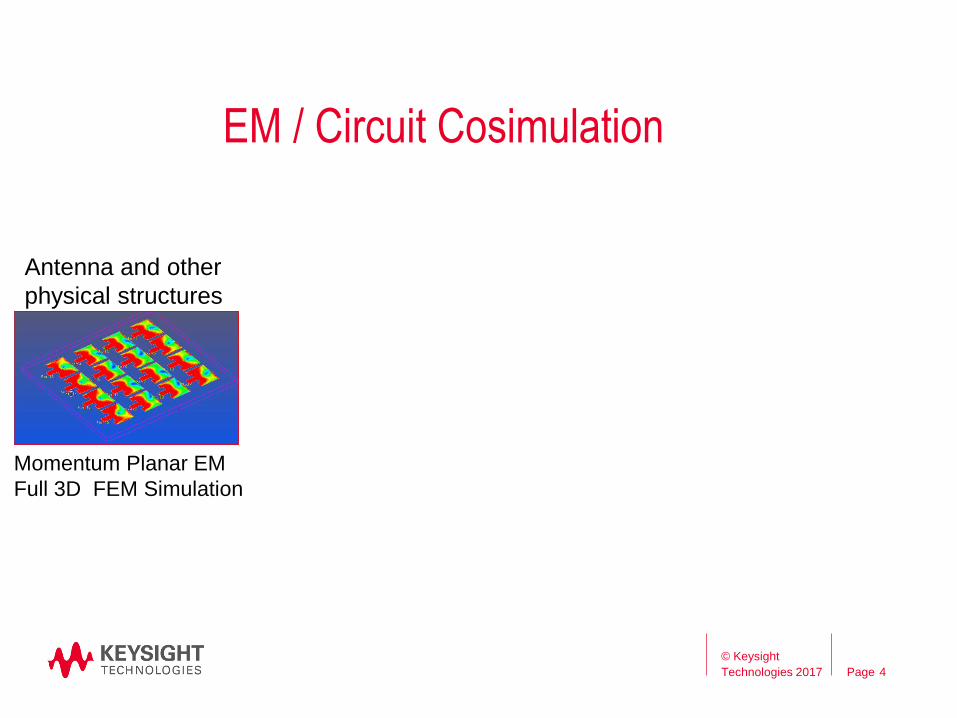
EM / Circuit Cosimulation
Antenna and other
physical structures
Momentum Planar EM
Full 3D FEM Simulation
© Keysight
Technologies 2017 4

PagePage 5
EM / Circuit Cosimulation
Antenna and other
physical structures
Momentum Planar EM
Full 3D FEM Simulation
+
Transceiver Components
Circuit level designs; X-parameter
models, EM models, etc.
© Keysight
Technologies 2017 5
HB, S-Par, Envelope, Tran, DC, AC

PagePage 6
EM / Circuit Cosimulation
Antenna and other
physical structures
Momentum Planar EM
Full 3D FEM Simulation
+
Transceiver Components
Circuit level designs; X-parameter
models, EM models, etc.
=
Complete EM / Circuit
Simulation and Analysis
Captures the excitation from
the T/R module and apply it
to the Antenna(s)
© Keysight
Technologies 2017 6
HB, S-Par, Envelope, Tran, DC, AC
The output from the circuit
simulation drives/excites the
Antenna ports

Page© Keysight
Technologies 2017
28 GHz Transmit Chain with Patch AntennaSystem / Circuit / EM Co-simulation and beam steering
7
Demo

Page© Keysight
Technologies 2017
Transmit Chain with Patch AntennaSystem / Circuit / EM Co-simulation and beam steering
Plextek RFI Buffer AmpPlextek RFI PAPower Divider
4X4 Array .5 Lambda
Patch Antenna28 GHz BPF
Phase Shifter
8

Page
28 GHz Power Divider
© Keysight
Technologies 2017
Page
9
Power Divider
Designed with:
TriQuint PHEMT process
9

Page© Keysight
Technologies 2017
Mm-Wave Small Signal Amps
mm-Wave small signal Amp
Designed with:
TriQuint PHEMT process
10

Page
28 GHz Filter Response
© Keysight
Technologies 2017
28 GHz BPF
11

Page
Mm-Wave Power Amplifier
© Keysight
Technologies 2017
Page
12
Plextek RFI PA
X-Parameter model
Designed with:
GCS InP_DHBT Process
12
Global Communications Semiconductors

Page© Keysight
Technologies 2017
X-Parameters
• Accurately captures all non-linearties
• Protects your IP
• Much faster simulation speed and trade-off analysis in hierarchical
system design and verification.
• Accurate load pull modeling capability
Circuit Topology
X-parameter Model
13

Page© Keysight
Technologies 2017
X-Parameters
Overlaid Results
Model (Red) Vs. Circuit (Blue)
14

Page
Mm-Wave Power Amplifier
© Keysight
Technologies 2017
Page
15
Plextek RFI PA
X-Parameter model
Designed with:
GCS InP_DHBT Process
Circuit Sim – Red
X-Par model – Blue
Pin / Pout and Phase Response of PA
15

Page
Creating 16 X-Par models of Varied Pout and Phase
© Keysight
Technologies 2017
0 degrees
16
Page
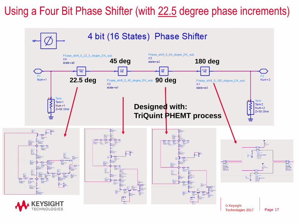
Using a Four Bit Phase Shifter (with 22.5 degree phase increments)
© Keysight
Technologies 2017
Designed with:
TriQuint PHEMT process
22.5 deg
45 deg
90 deg
180 deg
17

Page
Calculating Phase Shifter Phase Error
© Keysight
Technologies 2017
When circuit 1 is “ON”, circuit 2 is “OFF”
When circuit 1 is “OFF”, circuit 2 is “ON”
+5
- 5 +5
- 5
22.5 deg 22.5 deg
18

Page© Keysight
Technologies 2017
SS_Gain = 32.75 dB
LS_Gain = 31.65 dB @ Pin = -3 dBm (Pout = 28.65 dBm)
LS_Gain = 29.44 dB @ Pin = 1 dBm (Pout = 30.44 dBm)
Circuit level designs
HB Analysis
P -1dB = 28.65 dBm
@ Pin -3 dBm
19

Page
HB Analysis
© Keysight
Technologies 2017
SS_Gain = 40 dB
LS_Gain = 38.8 dB @ Pin = -10 dBm (Pout = 28.8 dBm)
LS_Gain = 37.2 dB @ Pin = -7 dBm (Pout = 30.2 dBm)
Behavioral level designs
P -1dB = 28.8 dBm
@ Pin -10 dBm
20

Page© Keysight
Technologies 2017
Patch Antenna Design
4.8 mm
3.2
8 m
m
1.14 mm
0.84 mm
0.5
8
mm
0.84 mm
Er=2.2 TanD=.0009H=.794 mm
21
Page
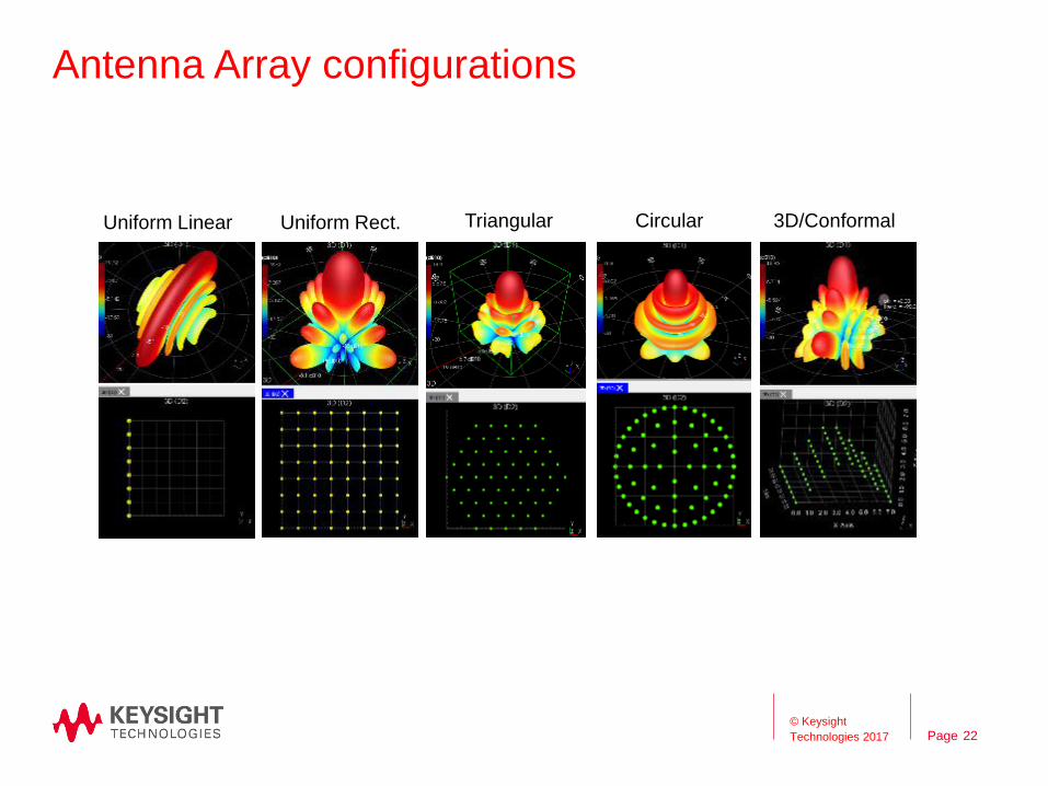
Antenna Array configurations
© Keysight
Technologies 2017
0 degrees
CircularUniform Rect. 3D/ConformalTriangularUniform Linear
22
Page© Keysight
Technologies 2017
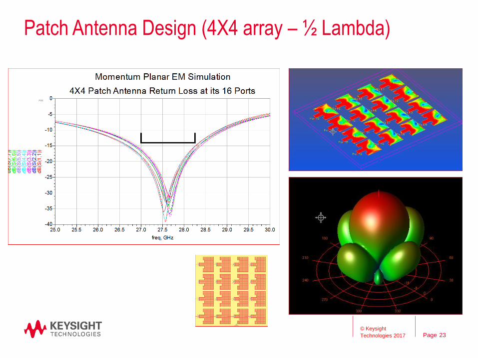
Patch Antenna Design (4X4 array – ½ Lambda)
23

Page
Applying Phase Shift to Antenna Ports
© Keysight
Technologies 2017
Page
24
http://www.radartutorial.eu/06.antennas/Phased%20Array%20Antenna.en.html
The main beam always points in the
direction of the increasing phase
shift.
Well, if the signal to be radiated is
delivered through an electronic
phase shifter giving a continuous
phase shift now, the beam direction
will be electronically adjustable.
However, this cannot be extended
unlimitedly. The highest value,
which can be achieved for the
Field of View (FOV) of a phased
array antenna, is 120° (60° left and
60° right). With the sine theorem the
necessary phase moving can be
calculated.
24

Page
Applying Phase Shift to Antenna Ports
© Keysight
Technologies 2017
Page
25
The phase shift Δφ between two
successive elements is constant
and is called phase-increment.
http://www.radartutorial.eu/06.antennas/Phased%20Array%20Antenna.en.html
25

Page
Applying Phase Shift to Antenna Ports
© Keysight
Technologies 2017
Page
26
Phase Shift Antenna look-up angle
61.5 degrees 20 degrees
31.2 10
22.5 7.2
26
Page
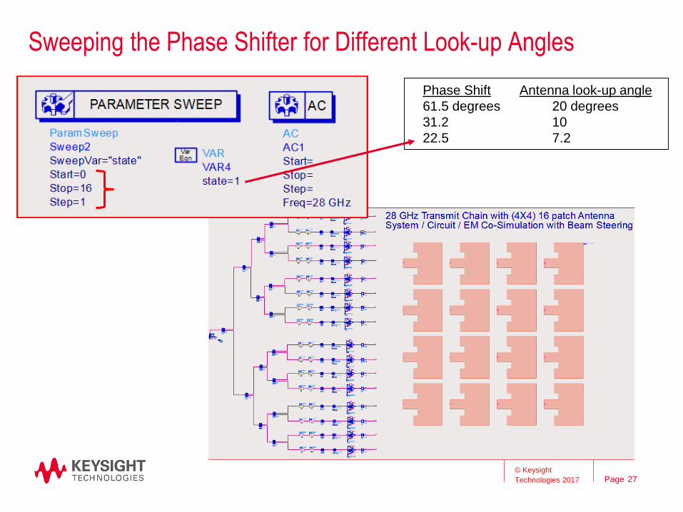
Sweeping the Phase Shifter for Different Look-up Angles
© Keysight
Technologies 2017
Phase Shift Antenna look-up angle
61.5 degrees 20 degrees
31.2 10
22.5 7.2
27
Page
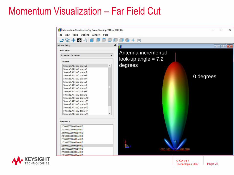
Momentum Visualization – Far Field Cut
© Keysight
Technologies 2017
0 degreesAntenna incremental
look-up angle = 7.2
degrees
0 degrees
28

Page
Momentum Visualization – Far Field Cut
© Keysight
Technologies 2017
Antenna incremental
look-up angle = 7.2
degrees
7.2 degrees
29

Page
Momentum Visualization – Far Field Cut
© Keysight
Technologies 2017
Antenna incremental
look-up angle = 7.2
degrees
14.4 degrees
30

Page
Momentum Visualization – Far Field Cut
© Keysight
Technologies 2017
21.6 degrees
31

Page
Momentum Visualization – Far Field Cut
© Keysight
Technologies 2017
28.8 degrees
32
Page
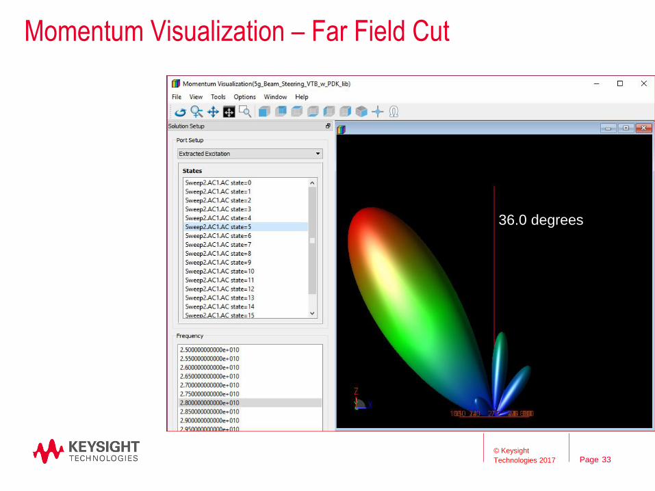
Momentum Visualization – Far Field Cut
© Keysight
Technologies 2017
36.0 degrees
33

Page
Momentum Visualization – Far Field Cut
© Keysight
Technologies 2017
43.2 degrees
34

Page
Momentum Visualization – Far Field Cut
© Keysight
Technologies 2017
50.4 degrees
35

Page
Momentum Visualization – Far Field Cut
© Keysight
Technologies 2017
57.6 degrees
The highest value, which
can be achieved for the
Field of View (FOV) of a
phased array antenna, is
120° (60° left and 60° right).
-57.6 degrees
36

Page
Momentum Visualization – Far Field Cut
© Keysight
Technologies 2017
- 50.4 degrees
37
Page
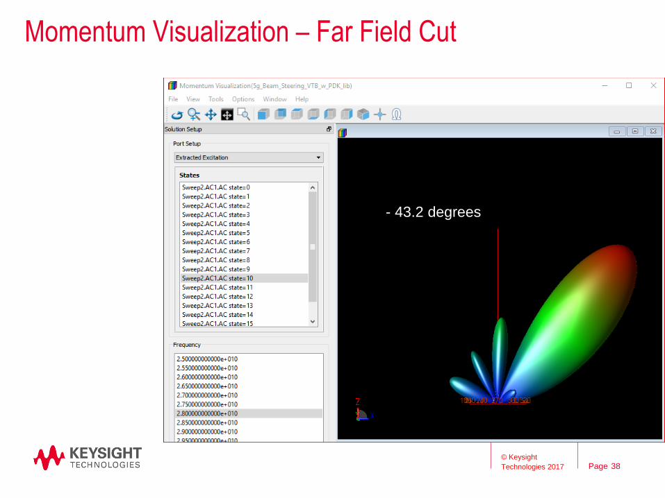
Momentum Visualization – Far Field Cut
© Keysight
Technologies 2017
- 43.2 degrees
38

Page
Momentum Visualization – Far Field Cut
© Keysight
Technologies 2017
- 36.0 degrees
39

Page
Momentum Visualization – Far Field Cut
© Keysight
Technologies 2017
- 28.8 degrees
40

Page
Momentum Visualization – Far Field Cut
© Keysight
Technologies 2017
- 21.6 degrees
41

Page
Momentum Visualization – Far Field Cut
© Keysight
Technologies 2017
- 14.4 degrees
42

Page
Momentum Visualization – Far Field Cut
© Keysight
Technologies 2017
- 7.2 degrees
43

Page
Momentum Visualization – Far Field Cut
© Keysight
Technologies 2017
0 degrees
44

Page
Harmonic Balance - Sweep Pin for each state
© Keysight
Technologies 2017
0 degrees
45
Swept power for each phase state

Page
Multi Band Systems
© Keysight
Technologies 2017
For Multi Band
Systems, select
the channel
frequency and
sweep the phase
46
Page
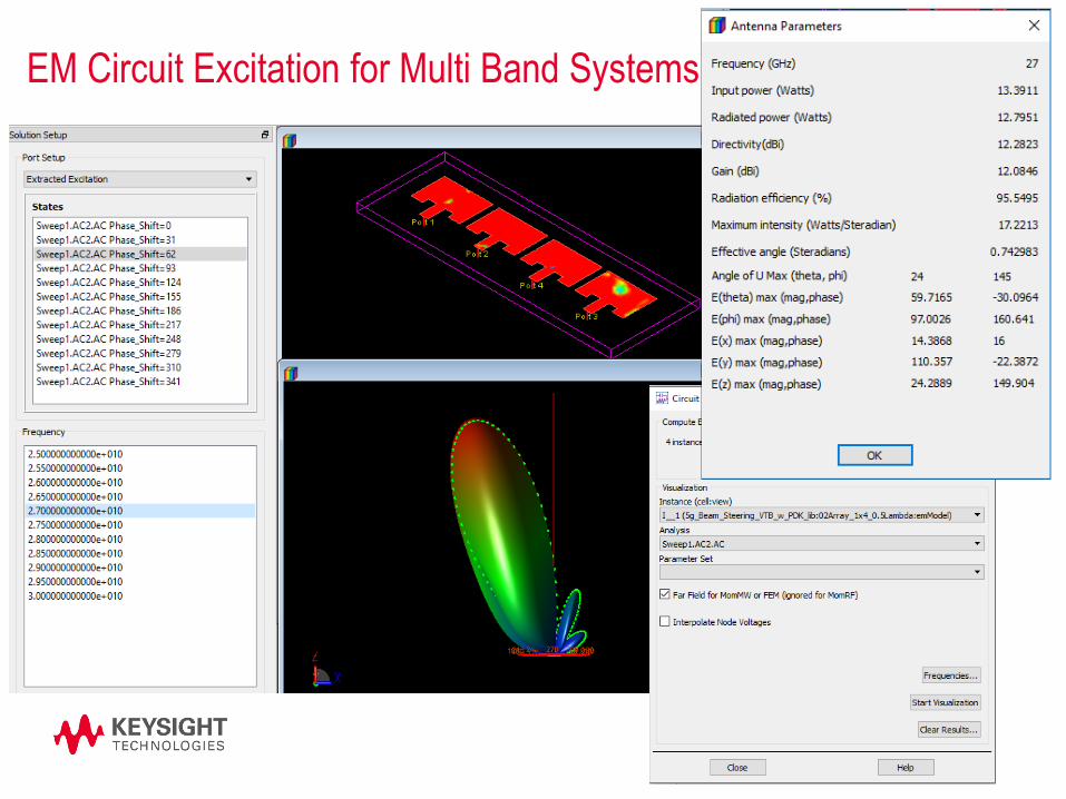
EM Circuit Excitation for Multi Band Systems
© Keysight
Technologies 2017Page 47
0 degrees
Page
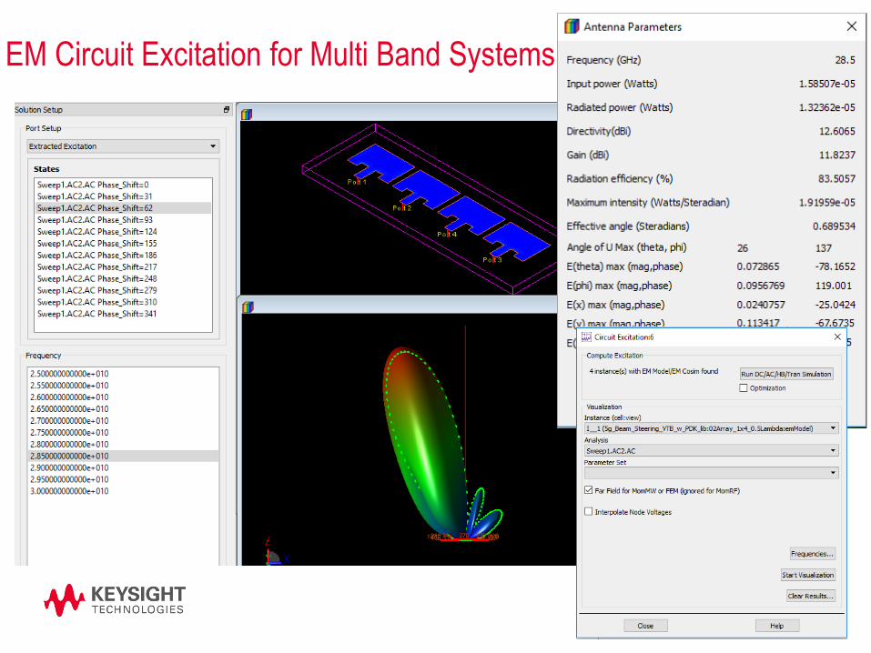
EM Circuit Excitation for Multi Band Systems
© Keysight
Technologies 2017Page 48
0 degrees

Page© Keysight
Technologies 2017 49
Switched Beam Systems and Isolation

Page
Four Channel Switched Beam System
© Keysight
Technologies 2017 50
28 GHz
28 GHz
28 GHz
28 GHz
Antenna 4
Antenna 3
Antenna 2
Antenna 1
Switch

Page
SP4T Pin Diode Switch
© Keysight
Technologies 2017
32 - 38 dB
isolation
< - 20 dB Return Loss
OnOffOffOff
51

Page
Effect of Isolation with SP4T Pin Diode SwitchGood isolation; low leakage
© Keysight
Technologies 2017 52
Antenna 2 (OFF)Antenna 1 (ON)
30.73 dBm
30.14 dBm
- .43 dBm
- 1.02 dBm

Page
Modeling the Switch in ADS
© Keysight
Technologies 2017 53
>30 dB isolation

Page
Using a Switch with 35 dB IsolationGood isolation; low leakage
© Keysight
Technologies 2017 54
Antenna 2Antenna 1
29.91 dBm
29.32 dBm
- 2.46 dBm
- 3.06 dBm
Good isolation
Page
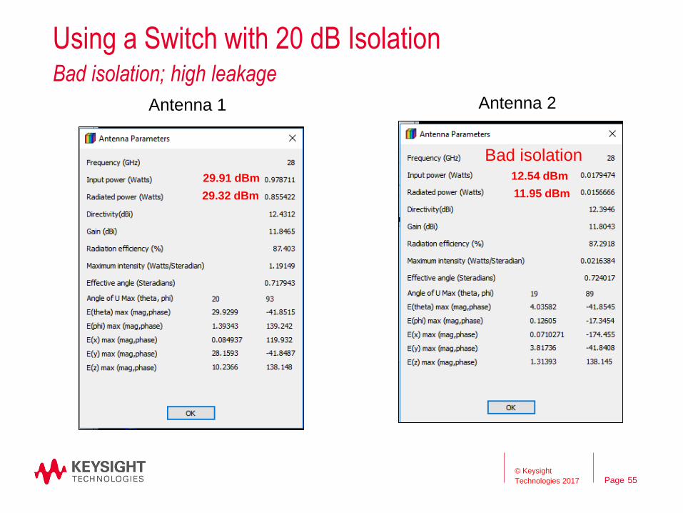
Using a Switch with 20 dB IsolationBad isolation; high leakage
© Keysight
Technologies 2017 55
Antenna 2Antenna 1
29.91 dBm
29.32 dBm
12.54 dBm
11.95 dBm
Bad isolation

Page
Using a Switch with 10 dB IsolationVery bad isolation; very high leakage
© Keysight
Technologies 2017 56
Antenna 2Antenna 1
29.89 dBm
29.31 dBm
22.54 dBm
21.95 dBm
Very bad isolation
Good isolation is important to have in components

Page© Keysight
Technologies 2017
5G Verification Test benches (VTB) in ADS
57
VTB is a regular component in the ADS simulation environment,
which is linked to the Verification Test Bench (VTB) in SystemVue.
VTBs enable circuit designers to make use of sources and
measurement setups from SystemVue and verify the performance of
a circuit using real world complex modulated signals conforming to
advanced wireless standards such as 2G/3G/4G/5G.

Page
5G FBMC Transmit Analysis VTB
© Keysight
Technologies 2017
Note: OFDM is the technology that has been selected by 3GPP rather than FBMC.
ADS 2017 plans to include this update. The VTB flow is the same.
58

Page
Pin = -50 dBm
SS Gain = 49 dB
5G FBMC Transmit Analysis VTB
59
© Keysight
Technologies 2017

Page© Keysight
Technologies 2017
Pin = -25 dBm SS Gain = 49 dB
LS Gain = 47.8 dB; 1.2 dB compressed
5G FBMC Transmit Analysis VTB
60

Page
Analysis
1. Effect of the Feed Network and Line Lengths
2. Effect of Varying PA’s AM / PM Response
3. Effect of Coupling and Cross talk
4. Effect of PA Dynamic Impedance with Antenna
61
© Keysight
Technologies 2017

Page
Analysis
1. Effect of the Feed Network and Line Lengths
2. Effect of Varying PA’s AM / PM Response
3. Effect of Coupling and Cross talk
4. Effect of PA Dynamic Impedance with Antenna
© Keysight
Technologies 2017 62

Page
Effect of Feeding Network and Line Lengths
© Keysight
Technologies 2017
Slide is taken from Dr. Gabriel Rebeiz’s
RFIC Symposium Plenary talk, June 2017
63

Page
System with identical PA’s and No Interconnect LinesNo added phase
© Keysight
Technologies 2017
To
Antenna
64

Page
System with identical PA’s and No Interconnect LinesNo added phase
© Keysight
Technologies 2017
Phase Shift = 0 deg
Side lobe 14.33 dB down
Null 34.9 dB down
65

Page© Keysight
Technologies 2017
Adding Short Interconnects from PA’s to Antenna
66

Page© Keysight
Technologies 2017
Phase Shift = 0 deg
Adding Interconnects from PA’s to Antenna mm
Side lobe 8.93 dB down (14.33 with no lines)
Null 18.75 dB down (34.9 with no lines)
67
Phase Shift = 0 deg
5 deg
shift

Page© Keysight
Technologies 2017
Phase Shift = 0 deg
Adding Longer Interconnects from PA’s to Antenna
Side lobe 10.63 dB down (14.33 with no lines)
Null 24.73 dB down (34.9 with no lines)
68
Phase Shift = 0 deg
28 deg
offset
3, 5, 7, 9 mm

Page
Analysis
1. Effect of the Feed Network and Line Lengths
2. Effect of Varying PA’s AM / PM Response
3. Effect of Coupling and Cross talk
4. Effect of PA Dynamic Impedance with Antenna
© Keysight
Technologies 2017 69
Page© Keysight
Technologies 2017
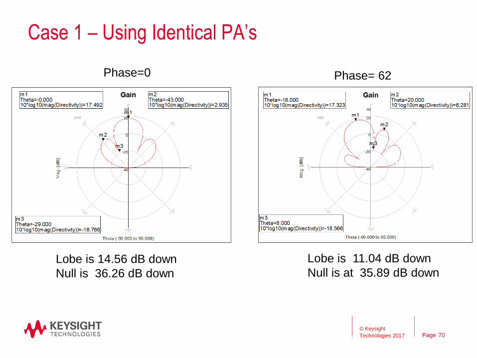
Lobe is 14.56 dB down
Null is 36.26 dB down
Lobe is 11.04 dB down
Null is at 35.89 dB down
Phase= 62Phase=0
Case 1 – Using Identical PA’s
70
Page
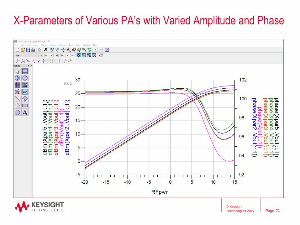
X-Parameters of Various PA’s with Varied Amplitude and Phase
© Keysight
Technologies 2017 71

Page© Keysight
Technologies 2017
Phase= 62Phase=0
Lobe is 12.813 dB down
Null is at 24.76 dB down
Lobe is 10.96 dB down
Null is at 24.28 dB down
Case 2 – Using Different PA’s
Compared with the case of identical PA’s
Lobe is 14.56 dB down
Null is 36.26 dB down
72

Page
© Keysight
Technologies 2017
With Different PA’sWith Identical PA’s
Lobe is 14.56 dB down
Null is 36.26 dB downLobe is 12.81 dB down
Null is 24.76 dB down
Summary: Response Using Identical PA’s Vs Different PA’s
73

Page
Important to Design Circuits with Small Variability
© Keysight
Technologies 2017
PA 1 Wide variation Smaller variation
Phase
Phase
PA 2
74

Page
Analysis
1. Effect of the Feed Network and Line Lengths
2. Effect of Varying PA’s AM / PM Response
3. Effect of Coupling and Cross talk
4. Effect of PA Dynamic Impedance with Antenna
© Keysight
Technologies 2017 75

Page
Coupling / Crosstalk between:
• Adjacent Channels
• PA’s
• Antenna elements
• Feed Lines and Antenna elements
© Keysight
Technologies 2017 76

Page
Response with No Coupling
© Keysight
Technologies 2017 77
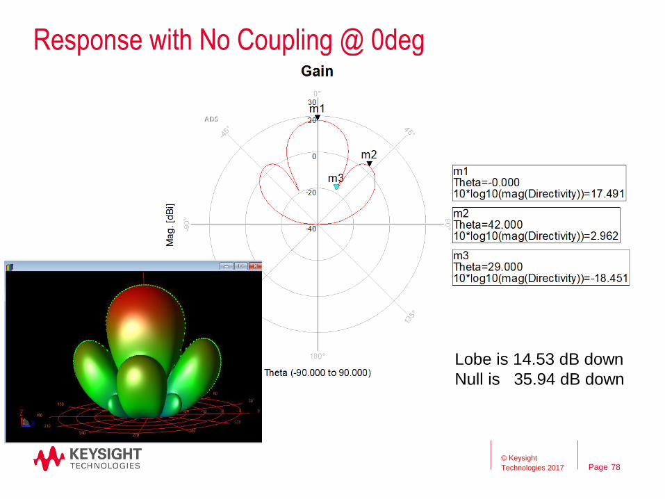
Page© Keysight
Technologies 2017
Response with No Coupling @ 0deg
Lobe is 14.53 dB down
Null is 35.94 dB down
78

Page
Response with Coupling
© Keysight
Technologies 2017 79

Page© Keysight
Technologies 2017
Response with Coupling 0deg
Lobe is 11.73 dB down
Null is 19.29 dB down
Compared with the case of no coupling
Lobe is 14.53 dB down
Null is 35.94 dB down
80
Page
Analysis
1. Effect of the Feed Network and Line Lengths
2. Effect of Varying PA’s AM / PM Response
3. Effect of Coupling and Cross talk
4. Effect of PA Loading and Change in Impedance
© Keysight
Technologies 2017 81

Page
Effect of scan angle
© Keysight
Technologies 2017
As scan angle increases :
– Effective cross-section area “A” of the array
decreases
• Less power to main lobe (lower peak gain)
• Less directivity (wider beam)
– PA loading & impedance changes
• Affects the final beam shape
• In extreme cases can create blind
spots
– More energy goes to side lobes (“grating
lobes”)
Watch out for unexpected interference
(pilot tones, jamming) and false echoes
(clutter) coming from unwanted directions
Q=45o
Q=0o
82

Page
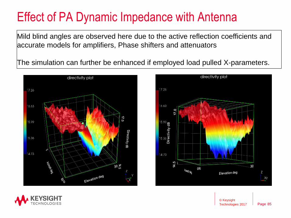
Effect of PA Dynamic Impedance with Antenna
© Keysight
Technologies 2017
From:
An Introduction to Phased Array Design
A Technical Note by N. Tucker
15/04/2011
83

Page
Effect of PA Dynamic Impedance with AntennaPhased Array system Architecture exploration
© Keysight
Technologies 2017
NumCols=8NumRows=8
Mode=SubArray
InsertionLoss=1 dBArraySplit1 {ArraySplit}
Tx
Rx
MainCarrierIndex=1
Phase=0 °Freq=2 GHz [Freq]
RxTx=TxArrayPort1 {ArrayPort}
Circuit_Link
Port_2Port_1
DesignName=XParamAmp
Subnetwork1 {Circuit_Link}
RxOutOrTxInMap=1RxInOrTxOutMap=2
DatasetName=HMC543ALC4B_sparm_25C_0.0.s2p
SParamSource=DataSetPhi=46 ° [myphi]
Theta=11 ° [mytheta]
CalcMode=AutoArrayPhase1 {ArrayPhase}
RxOutOrTxInMap=1RxInOrTxOutMap=2
DatasetName=HMC1019ALP4E_sparameters_deembedded_0.0p0dB.s…
SParamSource=DataSetNumBars=2
SideLobeLevel=-20 dB10
Window=TaylorArrayAttn1 {ArrayAttn}
RxTx=TxActiveLoading=Active Reflection Coefficients
ElementPatternFileName=D:\EMPROHOME\single_element_patter…ElementPatternType=Pattern FileDistanceY_in_Wavelengths=0.25
DistanceX_in_Wavelengths=0.25DistanceUnit=Wavelengths
NumElementsY=8NumElementsX=8
Configuration=Uniform Rectangular ArrayArrayAnt2 {ArrayAnt}
Source SplitterDigital
Attenuator
Digital
Phase
Shifter
AmplifierAntenna
Array
S-parametersMultiple
S-parameters
Multiple
S-parametersX-parameters Element patterns
Polarization
Coupling
Active impedance
1 8X8 8x8 8x8 8x8 8x8
84© Keysight
Technologies 2017
Page
Effect of PA Dynamic Impedance with Antenna
© Keysight
Technologies 2017
Mild blind angles are observed here due to the active reflection coefficients and
accurate models for amplifiers, Phase shifters and attenuators
The simulation can further be enhanced if employed load pulled X-parameters.
85

Page
5G 28-GHz Phased Array
Transceiver0.18um SiGe BiCMOS technology
© Keysight
Technologies 2017 86

Page
Full Phased Array Transceiver
© Keysight
Technologies 2017
Transmit Receive
87
LOS Link
10 Km

Page
SiGe BiCMOS Doherty Power Amplifier
© Keysight
Technologies 2017 88
Doherty PA
PA Output Power and Phase
Small Signal S-Parameters

Page
Transceiver Transmit Chain
© Keysight
Technologies 2017
Phase
ShiftersAmps
PA’s Filters
Transmit Patch
Antenna
LOS Link
10 Km
89
Page
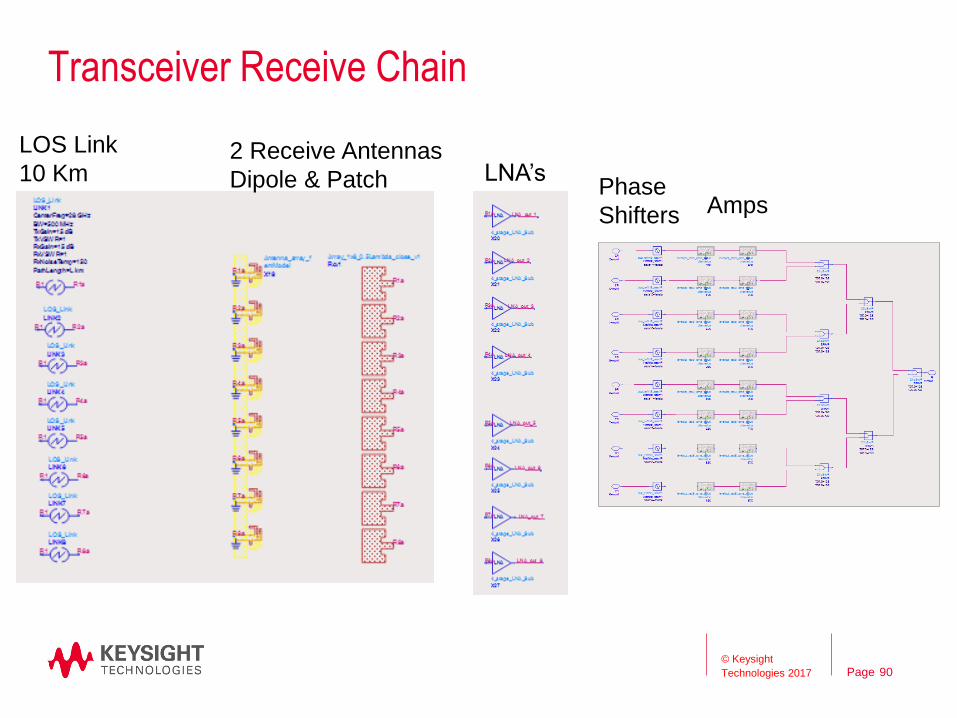
Transceiver Receive Chain
© Keysight
Technologies 2017
LNA’sPhase
Shifters Amps
2 Receive Antennas
Dipole & Patch
LOS Link
10 Km
90
Page
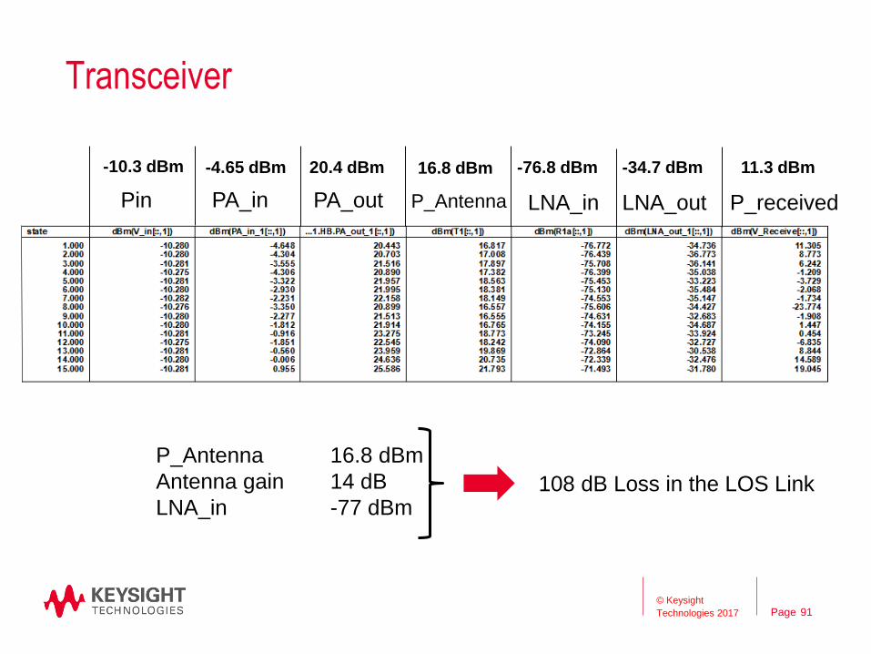
Transceiver
© Keysight
Technologies 2017
Pin PA_in PA_out P_Antenna LNA_in LNA_out P_received
-10.3 dBm -4.65 dBm 20.4 dBm 16.8 dBm -76.8 dBm -34.7 dBm 11.3 dBm
P_Antenna 16.8 dBm
Antenna gain 14 dB
LNA_in -77 dBm108 dB Loss in the LOS Link
91
Page
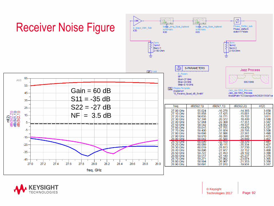
Receiver Noise Figure
© Keysight
Technologies 2017
Gain = 60 dB
S11 = -35 dB
S22 = -27 dB
NF = 3.5 dB
92

Page
Transmit Chain Verification Test Bench (VTB) for EVM
© Keysight
Technologies 2017 93

Page
Transmit Chain EVM
© Keysight
Technologies 2017 94
Page
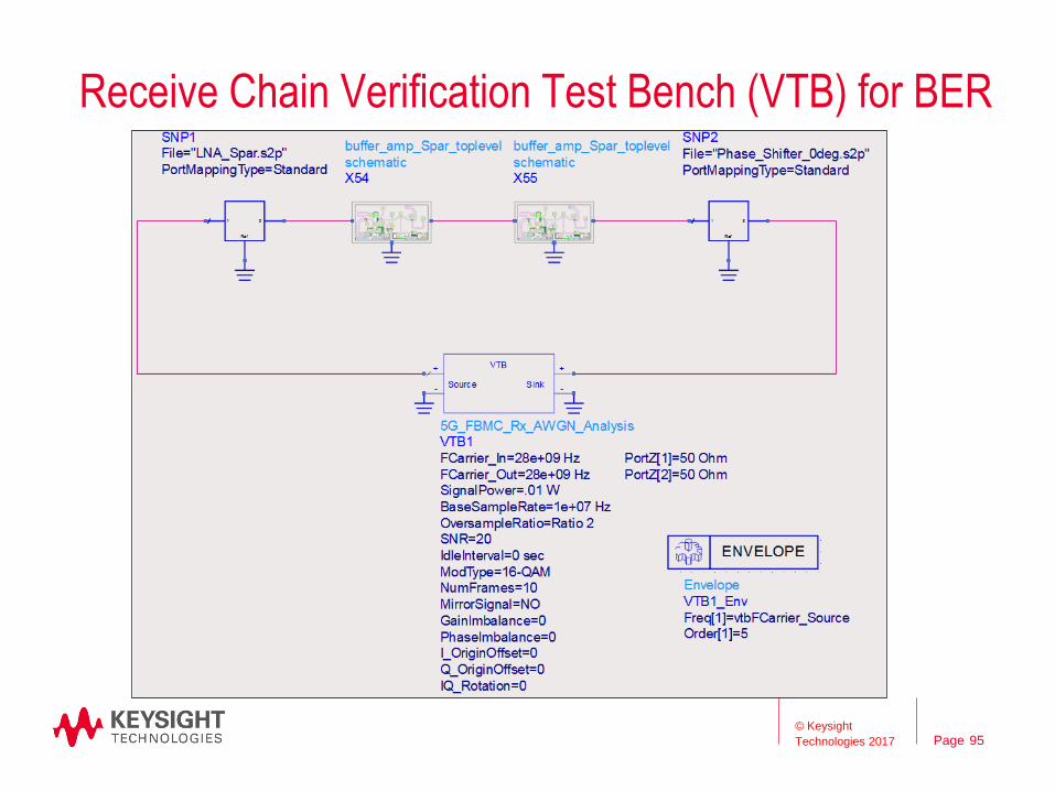
Receive Chain Verification Test Bench (VTB) for BER
© Keysight
Technologies 2017 95

Page
Receive Chain Verification Test Bench (VTB) for BER
© Keysight
Technologies 2017 96
Page
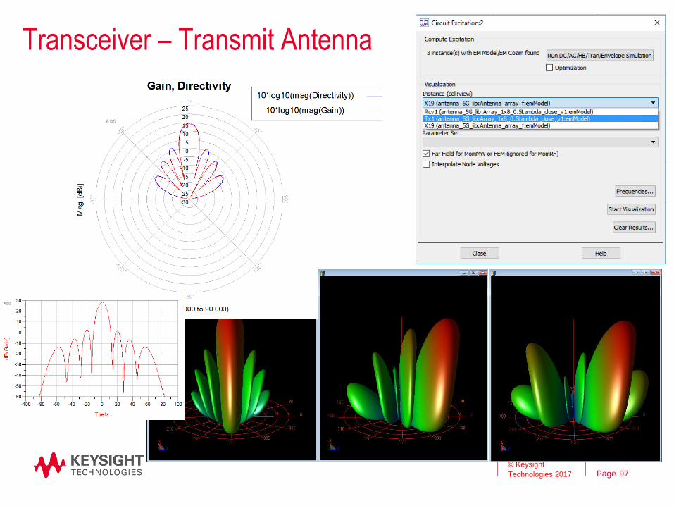
Transceiver – Transmit Antenna
© Keysight
Technologies 2017 97

Page
Transceiver – Receive Antenna 1
© Keysight
Technologies 2017 98

Page
Transceiver – Receive Antenna 2
© Keysight
Technologies 2017 99

Page
Future Work
© Keysight
Technologies 2017
EM Excitation in ADS 2016
EM Excitation in ADS 2017
Includes Circuit Envelope
Allows bringing in modulated 5G sources
from system view to perform full 5G analysis
100

Page
Acknowledgement
© Keysight
Technologies 2017
I extend my sincere gratitude to the following people who have
helped me put this project material together:
• Anil Panday
• Plextek RFI
• Rupam Anand
Special Thanks to the following people who have provided me with
feedback and support
• Carmina Stremlau
• How-Siang Yap
• Murthy Upmaka
• Bhumit Rojivadia (Intern)
• Sangkyo Shin
101
Page© Keysight
Technologies 2017
Conclusion
This webcast has demonstrated the importance of:
• EM/Circuit Co-simulation in 5G design and simulation
• Verification Test Bench (VTB) Simulation
• Analysis
➢ Effect of the Feed Network and Line Lengths
➢ Effect of Varying PA’s AM / PM Response
➢ Effect of Coupling and Crosstalk
➢ Effect of PA Dynamic Impedance with Antenna
• Transceiver Design Example
➢ Using Tower Jazz .18um SiGe BiCMOS technology
102
Page© Keysight
Technologies 2017
Conclusion
This webcast has demonstrated the importance of:
• EM/Circuit Co-simulation in 5G design and simulation
• Verification Test Bench (VTB) Simulation
• Analysis
➢ Effect of the Feed Network and Line Lengths
➢ Effect of Varying PA’s AM / PM Response
➢ Effect of Coupling and Crosstalk
➢ Effect of PA Dynamic Impedance with Antenna
• Transceiver Design Example
➢ Using Tower Jazz .18um SiGe BiCMOS technology
103

Page© Keysight
Technologies 2017 104
– “How To” Video Series
– Application Focused
(10 min each)
– Free workspace
www.keysight.com/find/eesof-how-to-videos
http://www.keysight.com/find/mytrial.rfmw.wc