design and operation principles of dc circuit breakers
TRANSCRIPT

Design and Operation Principles of DCCircuit BreakersDevelopment of a Solid State DC Breaker for
the NTNU/SINTEF Smart Grid and Renewable
Energy Laboratory
Eivind Ødegaard Norum
Master of Energy and Environmental Engineering
Supervisor: Elisabetta Tedeschi, ELKRAFTCo-supervisor: Kjell Ljøkelsøy, SINTEF Energi
Salvatore D'Arco, SINTEF Energi
Department of Electric Power Engineering
Submission date: January 2016
Norwegian University of Science and Technology


i
Problem Description
The goal of the work is to gain a deep understanding of the design principles and operation ofa DC circuit breaker through analytical calculations, simulation activities and lab-scaled exper-imental validation. In particular, the investigation will be focused on the design of a lab-scaledsolid state DC circuit breaker in the range of 700 V 100 A for the DC grid in the NTNU/SINTEFSmart Grid and Renewable Energy Lab. The work is targeted at development of simplified sim-ulation models in EMTP/PSCAD, experimental laboratory activities and the development onbasic design guidelines for DC circuit breakers.

ii

iii
Acknowledgments
This thesis is a contribution to the Protection and Fault Handling in Offshore HVDC Grids project(ProOfGrids), financed by the Norwegian Research Council’s RENERGI programme and indus-try partners (EDF, National Grid, Siemens, Statkraft, Statnett, Statoil and NVE). The work wascarried out in a collaboration between NTNU and SINTEF. In this regard, I would like to thankthe main supervisor and professor Elisabetta Tedeschi, research scientist and co-supervisorsfrom SINTEF Kjell Ljøkelsøy ans Salvatore D’Arco for their support. I would also like to thank tothe service lab and the workshop at the Department of Power Engineering NTNU for their helpwith organizing the laboratory work. Finally, I would like to thank my fellow students and SigurdJakobsen for their help and support.
E.Ø.N.

iv

v
Abstract
Exciting high voltage direct current (HVDC) transmission systems are mainly point-to-pointconnections. A multi-terminal HVDC grid consisting of three or more inter connected con-verter stations is suggested in order to increase the reliability, redundancy and flexibility in longdistant bulk power transmission. Similar to AC (alternating current) grids, a protection systemof HVDC-grids must be able to clear faults without affecting the remaining healthy parts of thegrid. Thus, there is a need for HVDC circuit breakers, in which development is challenging:
• The circuit breaker must interrupt the current typically within 5 ms.
• The circuit breaker itself must provide the zero current crossing, as no natural zero cross-ing is exciting in DC grids.
• The circuit breaker must dissipate the magnetic energy provided by the line inductance
• The circuit breaker must withstand residual overvoltages after current interruption
This master thesis describes the development of a solid state dc circuit breaker for the DCgrid in the NTNU/SINTEF Smart Grid and Renewable Energy Systems Laboratory. The DCbreaker main components are Insulated bipolar gate transistors (IGBT) and metal oxide varis-tors (MOV). Under normal operation the IGBTs are placed in series with the DC line. The currentcommutates the current into a parallel MOV if current interruption is demanded. The MOV pro-vides subsequently a counter voltage and forces the current to zero.
A test model was assembled initially and corresponding simplified PSCAD simulation modelwas developed in order to gain a deeply understanding of the operation of a DC breaker andfacilitate the selection of components and the design of the DC breaker for the SINTEF/NTNUlaboratory.
The selection of components for the DC breaker was based on the results from the experi-mental activities. In addition, corresponding ratings were obtained in an adjusted PSCAD model,which included an electro thermal equivalent circuit for temperature calculations.
A developed theoretical background including the components used in the DC breaker andgeneral techniques of DC current interruption supported the work. Design guidelines for HVDCbreaker based on the experiences from the work were also developed.

vi

vii
Sammendrag
Per i dag er flesteparten av likestrøms-kraftoverføringer (HVDC) punkt-til-punktforbindelser.Det er foreslått å knytte sammen flere fremtidige og nåværende forbindelser sammen til HVDC-nett, bestående av 3 eller flere omformerstasjoner. I HVDC-nett forventes å øke fleksibiliteten ogpåliteligheten sammenlignet med eksisterende lang distanse HVDC transmisjon. Vernsystemeti HVDC-nett vil måtte tilfredsstille tilsvarende krav som for konvensjonelle HVAC-nett, og måetter seleksjonskriteriet være i stand til raskt å klarere feil, f.eks. kortslutninger, slik at driftenav det resterende nettet forblir upåvirket. Følgelig vil det være et behov for HVDC-effektbryterehvis utvikling har flere utfordringer:
• Likestrøm (DC) har ingen naturlig null-gjennomgang og må genereres av bryteren selv.
• Feil i DC-nett utvikler seg svært raskt og kan påføre stor skade på resten av systemet somf.eks. på omformerstasjoene. Bryteren må derfor være i stand til å bryte strømmen ogklarerere feilen innen typisk 5ms.
• Bryteren må kunne absorbere den gjenværende magnetiske energien i den utkoblede lin-jen på grunn av induktans.
• Bryteren må ha en holdespenning høyere enn de transiente overspenninger som på grunnav induktans oppstår ved brytning strøm.
I denne masteroppgaven følges prosessen av konstruksjonen av en DC effektbryter til bruk i NT-NUs og SINTEFs laboratorium for smartgrid og fornybar energi. Krafttransistorer, i form av IG-BTer og metalloksidavledere som utfører strømbrytningen, utgjør hovedkomponentene. Tran-sistorene leder strømmen under normal drift, og vil under strømbrytning kommutere strøm-men inn i parallelle metalloksidavlederne. Avlederen sørger for at strømmen faller til null ved ågenerere motspenning, og absorberer den resterende magnetiske energien. En DC-kontaktorbenyttes for å opprette et fysisk isolerende skille etter at feilstrømmen er klarert. Som bak-grunnsmateriale presenter oppgaven en teoridel som tar for seg strømbrytning i DC-nett, deaktuelle komponentene og verktøy for termiske beregninger i form av en elektrotermisk kret-sekvivalent.
En forsøksmodell ble satt sammen i forkant av konstruksjonen av DC bryteren til bruk påNTNU/SINTEF-laboratoriet. Forsøkene som ble utført utført ga et grunnlag for en dypere forståelseav virkemåten til en DC-bryter og for å kunne velge ut egnede komponenter.
Dette arbeidet ble støttet av simuleringer av en forenklet modell utført i PSCAD. Kompo-nenter til DC bryteren ble valgt ut basert på erfaringene fra forsøksmodellen og simuleringer.Nye tilpassede simuleringer ble utført for å kunne gi indikasjon på forventet virkemåte og for åbestemme DC-bryterens merkedata.
Basert på erfaringer fra hele prosessen foreslås enkle retningslinjer for oppbygningen av DC-brytere i HVDC-sammenheng. Tilsvarende DC brytere som ble konstruert til NTNU/SINTEFlaboratoriet vurderes til å medføre for store effekttap på grunn av ledespenningsfallet over tran-sistorene. Det ble foreslått en utvidelse til en hybrid løsning bestående av ultra hurtige mekaniskebrytere i tillegg.

viii

ix
Acronyms
NTNU Norwegian University of Science and Technology
HVDC High voltage alternating current
AC Alternating current
DC Direct current
MOV Metal oxide varistor
PSCAD Power system computer aided design
EMTP Electromagnetic transient programming
VSC Voltage source converter
LCC Line commutated converter
MMC Modular muilti-level converter
IGBT Insulated bipolar gate transistor
GTO Gate turn-off thyristor
LCS Load commutation switch
UFD Ultra fast disconnecter
em f Electromotive force
TIV Transient interruption voltage
MOSFET Metal oxide semiconductor field effect transistor
ZnO Zinc oxide
SiC Silicon carbide
OHL Overhead line
CLR Current limiting reactor
BIGT Bi-mode insulated gate transistor
BS Bypass switch
CS Charging switch
IS Isolator switch
FPGA Field programmable gate array

x

xi
Symbols
Latin Alphabet
CDC DC capacitor voltage
CMOV MOV capacitance
Csnub Snubber capacitance
Cv Heat capacity
Cθ Thermal capacitance in elctro thermal circuits
Cθi Thermal capacitance in elctro thermal circuits of layer i
gm Forward transconductance
I Current
IC Collector current
ICr m Repetitive peak current
IC max Rated collector current
Il i ne Line current
Imax Maximum current interruption capability
Iswi tch Contactor current
Itr i p Detection trip level of the protetion system
I0 Peak line current
KMOV Ceramic material constant
LLC R Current limiting reactor inductance
Ll i ne Line inductance
Lload Load inductance
Lσ Stray Inductance
Pcond Heat conduction loss
PMOV max MOV maximum average power
PMOV MOV power
Ptot Maximum power dissipation of an IGBT

xii
Ploss Power loss
RD Discharge resistance
Rl oad Load resistance
RON On-state resistance
Rθ Thermal resistance
Rθ j a Thermal resistance from junction to ambient
Q Energy as heat
t Time
T Temperature
Ta Ambient temperature
taux Time interval from Vcoi l is set to 0 to Vaux is open circuited
T j Semiconductor junction temperature
tbr eak Break time, time form peak current to zero current
Tci r i t i cal MOV critical temperature
Tcase Case temperature
T j max Maximum junction temperature
TMOV MOV temperature
tpul se Pulse time
tstep Simulation step time
Tr esponse Response time of the protection system
tzer o Time interval from Vcoi l is set to 0 to Iswi tch = 0 V
Vaux Contactor auxiliary contacts voltage
VDC DC source voltage
VC B Circuit breaker voltage
Vc MOV Clamping voltage
VC E Collector-emitter voltage
VC E sat Collector emitter saturation voltage
xiii
VC Emax Rated collector-emitter voltage
VC Bmax Maxium DC breaker voltage
Vcoi l Contactor coil voltage
VDC Voltage source voltage
V f b Forward voltage base drop
V f c Forward voltage drop due to current conduction
VGE Gate-emitter voltage
VI .C Insulation coordination level
VMOV MOV voltage or rated operating voltage
Vmar g i n Voltage margin
Vl i ne Line voltage
Vswi tch Contactor voltage
VsnubMOV Snubber MOV voltage
WC snub Snubber capacitor energy
Vv Rated varistor voltage
Vw Withstand voltage
WC snub Snubber capacitor energy
Wl i ne Energy stored in the DC line
Wsour ce Energy provided by the voltage source
Wswi tchi ng l oss Total switching loss
WMOV MOV energy dissipation
WMOV max MOV maximum energy dissipation
Zθ Thermal transient impedance

xiv
Greek Alphabet
Φ Magnetic flux
α Non linearity exponent
λ Thermal conductivity
τ Time constant
τθi Thermal time constant of layer i

Contents
Problem Description . . . . . . . . . . . . . . . . . . . . . . . . . . . . . . . . . . . . . . . . iAcknowledgments . . . . . . . . . . . . . . . . . . . . . . . . . . . . . . . . . . . . . . . . . iiiAbstract . . . . . . . . . . . . . . . . . . . . . . . . . . . . . . . . . . . . . . . . . . . . . . . . vSammendrag . . . . . . . . . . . . . . . . . . . . . . . . . . . . . . . . . . . . . . . . . . . . viiList of Acronyms . . . . . . . . . . . . . . . . . . . . . . . . . . . . . . . . . . . . . . . . . . ixList of Symbols . . . . . . . . . . . . . . . . . . . . . . . . . . . . . . . . . . . . . . . . . . . xi
1 Introduction 11.1 Background . . . . . . . . . . . . . . . . . . . . . . . . . . . . . . . . . . . . . . . . . . 11.2 Objectives . . . . . . . . . . . . . . . . . . . . . . . . . . . . . . . . . . . . . . . . . . . 21.3 Limitations and Simplifications . . . . . . . . . . . . . . . . . . . . . . . . . . . . . . . 21.4 Methodology/Approach . . . . . . . . . . . . . . . . . . . . . . . . . . . . . . . . . . . 21.5 Contributions . . . . . . . . . . . . . . . . . . . . . . . . . . . . . . . . . . . . . . . . . 31.6 Structure of the Report . . . . . . . . . . . . . . . . . . . . . . . . . . . . . . . . . . . . 3
2 DC Grids 52.1 Defintion of DC Grids . . . . . . . . . . . . . . . . . . . . . . . . . . . . . . . . . . . . 52.2 Voltage Source Converters . . . . . . . . . . . . . . . . . . . . . . . . . . . . . . . . . . 62.3 Faults in DC Grids . . . . . . . . . . . . . . . . . . . . . . . . . . . . . . . . . . . . . . . 62.4 DC Grid Protection System . . . . . . . . . . . . . . . . . . . . . . . . . . . . . . . . . 72.5 DC Circuit Breaker Topologies . . . . . . . . . . . . . . . . . . . . . . . . . . . . . . . 8
3 Theoretical Background - General Electric Concepts 133.1 Magnetic Phenomena . . . . . . . . . . . . . . . . . . . . . . . . . . . . . . . . . . . . 133.2 Counter Voltage . . . . . . . . . . . . . . . . . . . . . . . . . . . . . . . . . . . . . . . . 143.3 Magnetic Energy . . . . . . . . . . . . . . . . . . . . . . . . . . . . . . . . . . . . . . . 143.4 Successful Interruption . . . . . . . . . . . . . . . . . . . . . . . . . . . . . . . . . . . 15
4 Theoretical Background - Basic Components 174.1 The Insulated Gate Bipolar Transistor . . . . . . . . . . . . . . . . . . . . . . . . . . . 174.2 Metal Oxide Varistor . . . . . . . . . . . . . . . . . . . . . . . . . . . . . . . . . . . . . 22
5 Theroretical Background - System Aspects 275.1 Stray inductance and Snubber Circuits . . . . . . . . . . . . . . . . . . . . . . . . . . 275.2 Thermal Design Considerations . . . . . . . . . . . . . . . . . . . . . . . . . . . . . . 285.3 Heat sinks, Thermal Grease and Cooling Medium . . . . . . . . . . . . . . . . . . . . 30
xv

xvi CONTENTS
6 Considerations and Description of Laboratory Work 336.1 NTNU/SINTEF Smart Grid and Renewable Energy Lab . . . . . . . . . . . . . . . . . 336.2 Solid State DC Circuit Breaker Test Model . . . . . . . . . . . . . . . . . . . . . . . . . 346.3 Contactor Switch Test . . . . . . . . . . . . . . . . . . . . . . . . . . . . . . . . . . . . 38
7 PSCAD DC Breaker Model 417.1 Software Description . . . . . . . . . . . . . . . . . . . . . . . . . . . . . . . . . . . . . 417.2 DC Breaker . . . . . . . . . . . . . . . . . . . . . . . . . . . . . . . . . . . . . . . . . . . 417.3 DC Grid . . . . . . . . . . . . . . . . . . . . . . . . . . . . . . . . . . . . . . . . . . . . . 427.4 Overcurrent Protection . . . . . . . . . . . . . . . . . . . . . . . . . . . . . . . . . . . . 437.5 Electro Thermal Circuit . . . . . . . . . . . . . . . . . . . . . . . . . . . . . . . . . . . 44
8 Results 458.1 Objective of Results Analysis . . . . . . . . . . . . . . . . . . . . . . . . . . . . . . . . 458.2 Laboratory Test Model Results . . . . . . . . . . . . . . . . . . . . . . . . . . . . . . . 458.3 Contactor Switch Test . . . . . . . . . . . . . . . . . . . . . . . . . . . . . . . . . . . . 558.4 Comparison with the Preliminary Simulation Results . . . . . . . . . . . . . . . . . . 578.5 PSCAD Simulation Model Adjustment . . . . . . . . . . . . . . . . . . . . . . . . . . . 59
9 Development of the DC Breaker Design 619.1 Corner Cases . . . . . . . . . . . . . . . . . . . . . . . . . . . . . . . . . . . . . . . . . . 619.2 Discussion of the Results for the Final DC Breaker Design . . . . . . . . . . . . . . . 629.3 DC Breaker Ratings . . . . . . . . . . . . . . . . . . . . . . . . . . . . . . . . . . . . . . 659.4 Selection of Components . . . . . . . . . . . . . . . . . . . . . . . . . . . . . . . . . . 659.5 PSCAD Simulations and Determination of Ratings . . . . . . . . . . . . . . . . . . . 67
10 Implementation of the DC Breaker 7510.1 Configuration of the DC Breaker . . . . . . . . . . . . . . . . . . . . . . . . . . . . . . 7510.2 Construction of DC breaker . . . . . . . . . . . . . . . . . . . . . . . . . . . . . . . . . 7610.3 Function Test . . . . . . . . . . . . . . . . . . . . . . . . . . . . . . . . . . . . . . . . . 76
11 Guidelines for DC Breaker Design 8111.1 Circuit Breakers for HVDC Applications . . . . . . . . . . . . . . . . . . . . . . . . . . 8111.2 HVDC Breaker Design . . . . . . . . . . . . . . . . . . . . . . . . . . . . . . . . . . . . 83
12 Discussion, Conclusion and Further work 8912.1 Discussion and Conclusion . . . . . . . . . . . . . . . . . . . . . . . . . . . . . . . . . 8912.2 Further Work . . . . . . . . . . . . . . . . . . . . . . . . . . . . . . . . . . . . . . . . . . 92
A SIEMENS IGBT: BSM 300 GA 120 DN2 93
B Time Delay of Contactor Switch 105
C Calculations 109
D Snubber Capacitor Discharge 111
E Maximum Current Breaking Capability 113

CONTENTS xvii
F DC breaker circuit diagrams 117
Bibliography 121

xviii CONTENTS

Chapter 1
Introduction
1.1 Background
Renewable energy resources such as wind, solar and hydro power have gained considerableinterest in recent years. Massive exploitation of these resources typically requires long distantbulk power transmission from remote areas, where high voltage direct current (HVDC) is theonly feasible option [1]. Present HVDC systems are mainly point to point connections, butdevelopment of multi-terminal meshed HVDC grids is suggested and may contribute to increasethe power system flexibility, reliability and redundancy and also reduce the number of converterstations [2]. However one of the obstacles of realizing such grids is the need for a protectionsystem to minimise the effects of faults [3]. In excising HVDC point to point connections faultsare cleared from the AC (Alternating Current) side of the converter stations. A protection systemof a HVDC grid must also comply with the selectivity criterion as in present AC grids whichprovides the demand for HVDC circuit breakers [4].There are several challenges related to the development of HVDC Circuit breakers [5, 2, 6]:
• The rise of the fault current in DC (Direct Current) grids is very high compared to AC gridsbecause the low line impedance of DC lines. Accordingly, the DC breaker must interruptthe current typically within 5 ms.
• In AC grids the arc in the circuit breaker under current interruption is extinguished bythe zero current crossing which is provided naturally by the system. In DC grids the zerocurrent crossing must be provided by the circuit breaker itself.
• Unlike AC girds, the magnetic energy of DC grids is stored in the system inductance. TheDC circuit breaker must dissipate this energy.
• The DC breaker must withstand the residual overvoltages after the current interruption.
There are promising HVDC breaker topologies suggested from ABB and ALSTOM. They differfrom AC circuit breakers as they are based on semiconductor technology, metal oxide varistors(MOV) and ultra-fast switches [5, 7]. A simplified version of these topologies is the solid stateDC circuit breaker. A lab scaled type for research applications will be developed for the DC gridin the NTNU/SINTEF Smart Grid and Renewable Energy Lab.
1

2 CHAPTER 1. INTRODUCTION
1.2 Objectives
The main objectives of this thesis are:
• Develop a theoretical background for the design of DC circuit breaker.
• Assemble a lab-scaled solid state DC circuit breaker test model.
• Design a lab-scaled solid state DC circuit breaker for the DC grid in NTNU/SINTEF SmartGrid and Renewable Energy Lab.
• Develop simulation models in EMTP/PSCAD of the lab-scaled DC circuit breaker testmodel and of the lab-scaled solid state breaker for the DC grid in NTNU/SINTEF SmartGrid and Renewable Energy Lab
• Develop guidelines for the design of a high voltage DC circuit breaker on the basis on theexperimental work, simulations and design process.
1.3 Limitations and Simplifications
The following limitations of scope and simplifications are considered in this work:
• A DC grid is represented by an inductance and a resistor. Travelling waves and distributedparameters are not considered in the emulation of DC grids.
• The AC/DC converters stations are represented as DC voltage sources or capacitor banks.Harmonics, ripple and control system of the DC grid representation are omitted.
• The work is carried out practically with simplified analytic calculations. Advanced analyticcalculations for DC systems are omitted.
• Semiconductor physics are briefly considered.
• The control of the solid state breaker is manual, the focus is on the operation of the elec-trical aspects DC breaker and not the protective relays.
• Thermal modelling is carried out in one dimension.
• The protection system of the converters are not considered. The emphasis is on the pro-tection from line faults.
1.4 Methodology/Approach
Initially a theoretical background will be established with emphasis on the requirements of DCcircuit breakers in a DC grid, the separate components and the challenges related to them.
To facilitate the selection of the components for the lab-scaled solid state DC circuit breakerfor the NTNU/SINTEF Smart Grid and Renewable Energy Lab, a test model will be assembled

1.5. CONTRIBUTIONS 3
and tested experientially. The experimental work with the test model is supported by prelimi-nary simulations in EMPT/PSCAD. The simulations will thereafter be adjusted according to theexperimental results from the test model to obtain a realistic, but simplified DC breaker simula-tion model.
The results from experimental work and the simulations will be analysed in order to deter-mine the components of the solid state DC circuit breaker for the NTNU/SINTEF Smart Gridand Renewable Energy Lab and development of basic guidelines for DC circuit breaker designfor high voltage applications. MATLAB will be used for processing results from EMPT/PSCADand experimental work.
1.5 Contributions
The result of the work contributes with a detailed analysis and insight of the operation of solidstate DC circuit breakers. A final lab-scaled prototype DC-breaker is developed, that is usefulfor further research on HVDC multi-terminal grids at the NTNU/SINTEF Smart Grid and Re-newable Energy Laboratory.
1.6 Structure of the Report
Chapter 2: Background information of DC grids and DC breaker topologies.
Chapters 3, 4 and 5: Theoretical background in terms of the components, system aspects andcurrent interruption in DC grids.
Chapter 6: Brief description of the NTNU/SINTEF Smart Grid and Renewable Energy Lab andthe implementation the DC breaker test model for experimental activities.
Chapter 7: Considerations and development of PSCAD simulation models.
Chapter 8: The results from experimental work with the test model and results from PSCADsimulations.
Chapter 9: Selection of the components for the DC breaker intended for use in the NTNU/SINTEFSmart Grid and Renewable Energy Lab. Determination of the expected rating.
Chapter 10: Implementation of he DC breaker with description of configuration and a functiontest.
Chapter 11: Guidelines for DC breakers for high voltage applications based on experiences withthe development of the DC breaker.
Chapter 12: Discussion, conclusion and suggestions for further work.

4 CHAPTER 1. INTRODUCTION

Chapter 2
DC Grids
This chapter introduces the concept of DC grids briefly. The key aspects of faults and DC circuitbreaker is described in order to provide some background information. High voltage power sys-tem applications are emphasised, as the DC grid in NTNU/SINTEF Smart Grid and RenewableEnergy Lab is intended to emulate a HVDC transmission system.
2.1 Defintion of DC Grids
Applications of DC grids have a wide area and may vary from medium voltage power system onships, low voltage solar powered micro grids in remote areas [8] to a high voltage "supergrid"connecting Europe, Middle-East and northern Africa [6].A multi-terminal HVDC grid system is defined by CIGRE as a HVDC transmission system con-nected to more than 2 converter stations [9]. An example of a simple DC grid is shown in fig-ure 2.1, which depicts an offshore wind farm power plant connected with 3 converter stationsonshore. In the introduction the motivation for such grids were mentioned briefly, and theHVDC circuit breaker is regarded as one of the key components for the development [2].
Figure 2.1: Example of a DC grid connected to an offshore wind power plant [4]
5
6 CHAPTER 2. DC GRIDS
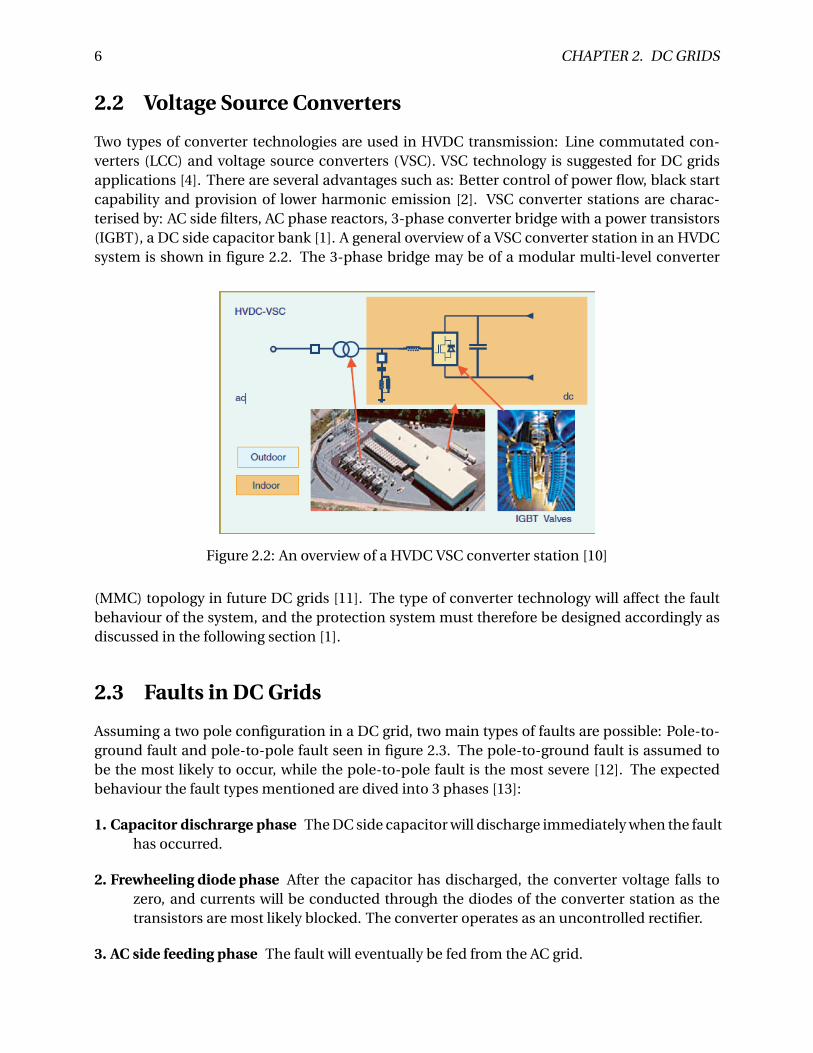
2.2 Voltage Source Converters
Two types of converter technologies are used in HVDC transmission: Line commutated con-verters (LCC) and voltage source converters (VSC). VSC technology is suggested for DC gridsapplications [4]. There are several advantages such as: Better control of power flow, black startcapability and provision of lower harmonic emission [2]. VSC converter stations are charac-terised by: AC side filters, AC phase reactors, 3-phase converter bridge with a power transistors(IGBT), a DC side capacitor bank [1]. A general overview of a VSC converter station in an HVDCsystem is shown in figure 2.2. The 3-phase bridge may be of a modular multi-level converter
Figure 2.2: An overview of a HVDC VSC converter station [10]
(MMC) topology in future DC grids [11]. The type of converter technology will affect the faultbehaviour of the system, and the protection system must therefore be designed accordingly asdiscussed in the following section [1].
2.3 Faults in DC Grids
Assuming a two pole configuration in a DC grid, two main types of faults are possible: Pole-to-ground fault and pole-to-pole fault seen in figure 2.3. The pole-to-ground fault is assumed tobe the most likely to occur, while the pole-to-pole fault is the most severe [12]. The expectedbehaviour the fault types mentioned are dived into 3 phases [13]:
1. Capacitor dischrarge phase The DC side capacitor will discharge immediately when the faulthas occurred.
2. Frewheeling diode phase After the capacitor has discharged, the converter voltage falls tozero, and currents will be conducted through the diodes of the converter station as thetransistors are most likely blocked. The converter operates as an uncontrolled rectifier.
3. AC side feeding phase The fault will eventually be fed from the AC grid.

2.4. DC GRID PROTECTION SYSTEM 7
(a) Pole to ground fault
(b) Pole to pole fault
Figure 2.3: Types of faults in a DC grid [4]
A detailed study of the Transient fault current in VSC HVDC grids is found in [14]. In the men-tioned reference, travelling wave phenomena are also simulated in PSCAD/EMTP. The currentthrough a DC circuit breaker under a pole-to-ground fault, obtained from the simulations, isshown in figure 2.4. The contributors to the fault current are depicted, in the figure: Area A)
Figure 2.4: Fault current through a DC circuit breaker with a pole to ground fault 100 km awaysimulated in PSCAD [14]
represents the current contribution from the DC capacitor, B) from the adjacent cable feederand both C) and D) from different converter stations in the model simulated. The intention pre-senting figure 2.4 is to show the contributions to the fault current and a steep rise up to 7-8 puwithin the first 2 ms.
2.4 DC Grid Protection System
The function for a protection system is to protect of the system itself and its user against damagewhile provide a reliable supply [1]. A power system protection scheme, regardless of AC or DC,

8 CHAPTER 2. DC GRIDS
should provide the properties or criteria listed in [4]. The criteria in particular concerning DCbreakers are:
Selectivity States the demand for DC circuit breakers in general, the protection system must beable to isolate faulted parts of the system only.
Speed States the demand for the DC circuit breaker to operate before the fault current damagesthe power system system and its users.
Reliabilty States the requirement for the DC circuit breakers in the system to be able to conductits required function under different modes and scenarios that may occur in DC grid.
The speed criterion provides some challenges due to fast rising fault currents seen in last sectionand in the introduction. The fault currents in DC grid may rapidly damage the free-wheelingdiodes of the converter stations and thus the DC breaker should operate before the event ofdiode damage is likely to occur. As stated in the introduction, the protection system must clearthe fault within a few ms.
2.5 DC Circuit Breaker Topologies
The DC circuit breaker topologies may be divided into three main types [1]:
1. Resonance DC breakers
2. Solid state DC breakers
3. Hybrid DC breakers
2.5.1 Resonance DC Circuit Breakers
Attempts to develop resonance HVDC circuit breakers were made as early in the 1980s’ [1]. Anoutline of the topology is shown in figure 2.5. The topology consist of mechanical switches andinterrupts the current when a zero crossing is generated with the help of a capacitive-inductivecurrent path (commutation current path) in parallel with the main mechanical switch. Thetopology also includes an absorbing branch consisting of MOVs. The technology has beenproven too slow for fault current interruption in DC grid based on VSC technology [2]. Theresonance topology may still provide useful applications such as load switching as it has a lowresistive on-state loss compared to newer topologies mentioned in this section [15]. The treemain branches of the resonance DC breaker topology are:
1. The nominal current path
2. The current commutation path
3. The energy absorption/dissipation path

2.5. DC CIRCUIT BREAKER TOPOLOGIES 9
mechanical switch
CL
U
Nominal current path
Commutation current path
Energy absorption/dissipation path
Figure 2.5: Resonance DC circuit breaker topology [1]
Under normal operation the current is flowing through the nominal current path. If the breakerreceives an interruption command, the mechanical switch will open and arc will occur and cur-rent will start to commutate into the commutation path. At this stage, the current oscillationsare generated. The voltage drop of the arc contributes to generate current oscillations due tothe commutation path which will provide the zero current crossing and eventually extinguishthe arc. Thereafter, the current will flow into absorption path in order to dissipate the residualmagnetic energy in the system.
2.5.2 Solid State DC Circuit Breakers
The solid state topology consists of semiconductor devices such as the insulated gate bipolartransistor (IGBT) or gate turn-off thyristor (GTO) and parallel MOVs [15]. Under normal oper-ation the current flows through the devices. To interrupt the current, the devices are switchedoff and current is commutated into the parallel MOV which here function both as the commu-tation path and the energy absorbing path. Similar to the resonance topology, the MOV willdissipate the energy stored in the system. Figure 2.6 depicts an example of a solid state topologywith the use of IGBT and diodes for bi-directional applications. In figure 2.6 a solid state DC
Figure 2.6: Solid state DC circuit breaker topology [13]

10 CHAPTER 2. DC GRIDS
breaker for one directional current interruption is shown. Bi-directional current interruption isachieved by placing a similar IGBT with an anti-parallel diode in anti-series. More breaker cellsmay be placed in series to increase the rated voltage level. The solid state state circuit breakerhas proven to break current with the required speed for fault current interruption. But as thesemiconductors are conducting current under normal operating conditions, the losses due tothe voltage drop over the breaker will be high especially in high voltage applications [15, 13].The DC breaker intended in the DC gird in the NTNU/SINTEF lab is a lab-scaled solid state DCcircuit breaker. Unless other topologies stated in further chapters, a solid state DC breaker isrefereed to as DC breaker.
2.5.3 Hybrid DC Circuit Breakers
Hybrid topologies consists of both mechanical switches and semiconductor devises. There areexisting different topologies suggested which are surveyed in [16]. ABB and ALSTOM have de-veloped HVDC circuit breaker prototypes which are presented as promising technologies in re-cent research literature [5, 7]. Figure 2.7 depicts the main outline of the circuit breaker. Thebreaker may be seen as an extension of an IGBT based solid state topology, since the breaker es-sentially has an additional branch with a mechanical low-ohmic ultra fast disconnecter (UFD)and a load commutation switch (LCS). The LCS is also a solid state DC breaker, but has onlysufficient breaker cells in order to commutate the current into the main breaker. The Hybrid
Figure 2.7: ABB hybrid HVDC circuit breaker topology [5]
topology overcomes the issue with conduction losses of the solid state topology by letting nom-inal current under normal operation flow through a nominal current path consisting of the LCS,and a UFD indicated in figure 2.7. When the circuit breaker receives an interruption command,the LCS switches off and commutates the current into the main breaker similar to the solid statebreaker. After the commutation, the UFD opens and creates a physical isolation, protecting theLCS from the voltage drop when the main breaker interrupts current. The UFD is a key compo-nent to keep the losses under normal operation as low as possible and obtaining the fast currentinterruption needed. The UFD is an electromagnetic actuator, using magnetic forces in orderto obtain the fast switching speed required. The operation and structure of a UFD is describedin detail in [17]. ABB claims that their HVDC circuit breaker is able to clear faults within in 5

2.5. DC CIRCUIT BREAKER TOPOLOGIES 11
ms [18]. In figure 2.7 a current limiting reactor (CLR) is shown which is an auxiliary series induc-tance with the line. The function of a CLR is to limit a high slope of the fault current. A switch inparallel with the hybrid dc breaker is also indicated which provides physical isolation after thefault current has been cleared.

12 CHAPTER 2. DC GRIDS
Chapter 3
Theoretical Background - General ElectricConcepts
The following three chapters(chapter 3-5), outline the theoretical background for the design andoperation of a DC breaker. This includes phenomena that cause issues related to fault currentinterruption as well as physical components used for DC breaker applications.
3.1 Magnetic Phenomena
Before defining the transient interruption voltage (TIV), the definition of inductance and Fara-day’s law is described to illustrate the connection with basic electromagnetic laws.
3.1.1 Inductance
Inductance is a physical quantity defined in [19] as the ratio of total flux linkages NΦ to thecurrent which they link I :
L = NΦ
I(3.1)
When a circuit segment with inductive properties experiences a change in the current, the link-ing flux will also change and provide time varying flux linkage. According to Faraday’s law thiswill induce a counter electromotive force (em f ):
em f =−d NΦ
d t(3.2)
Equation 3.3, which combines 3.2 and 3.1, is applicable for circuit calculations:
Vl i ne = Ll i ned Il i ne
d t(3.3)
The equation states that interruption of DC currents will induce negative voltages in the linesconnected to the DC-breaker due to time-varying magnetic field related to decreasing currents.
13

14 CHAPTER 3. THEORETICAL BACKGROUND - GENERAL ELECTRIC CONCEPTS
3.1.2 Transient Interruption Voltage
The simplified DC grid model shown in figure 3.1 is used to illustrate the transient interruptionvoltage (TIV) phenomenon. Assuming a fault occurs and the load Rl oad is short circuited: Theideal DC breaker quickly interrupts the fault current resulting in high and negative current sloped Il i ne /d t . This induces an overvoltage in the line Ll i ne , according to equation 3.3. The overvolt-age is referred to as the transient interruption voltage, analogous to transient recovery voltage inAC circuit breakers [7]. The relation in equation 3.3 is also important in terms of fault clearancetime since it states that the TIV and fault-clearance time are inverse quantities.
Ll i ne
+ −Vl i ne
Il i neDC breaker
+ −VC B
Rload
+−VDC
Figure 3.1: DC grid model with an ideal circuit breaker
3.2 Counter Voltage
The counter voltage principle describes an approach for forcing the DC current to zero. UnlikeAC grids, there is no zero-current crossing provided naturally by the system. With regard to thefigure 3.1, the slope of the current in the presence of short circuited load may be expressed as:
d Il i ne
d t= VDC −VC B
Ll i ne(3.4)
VC B >VDC ⇒ d Il i ne
d t< 0 (3.5)
The equations 3.4 and 3.5 states that slope of the fault current will depend on the the DC breakervoltage. In order to force the current to zero, the DC-breaker must provide a counter voltagehigher than the system voltage to ensure a negative voltage over the line inductance Ll i ne . Asuggested solution for a DC breaker is to provide the counter voltage with metal oxide varistors(MOV)[2].
3.3 Magnetic Energy
The stored magnetic energy in the inductive line segment Wl i ne during a fault can be expressedas:
Wl i ne =1
2Ll i ne I 2
0 (3.6)
Where I0 is peak current of Il i ne . During the fault interruption, when the current decreases, thevoltage source continues to deliver energy into to system [20]. This energy can be expressed as:
Wsour ce =∫ t1
0VDC Il i ne d t (3.7)

3.4. SUCCESSFUL INTERRUPTION 15
If a constant DC source voltage is assumed, equation 3.7 can be rewritten as:
Wsour ce =Ll i neVDC I 2
0
2(VC B −VDC )(3.8)
The total energy the DC breaker must dissipate is then be expressed as:
Wtot = 1
2Ll i ne I 2
0 (1+ VDC
(VC B −VDC )) (3.9)
3.4 Successful Interruption
For successful current interruption, a DC breaker must both be capable to dissipate the mag-netic energy stored in the system and withstand the TIV by providing a counter voltage. In ACcircuit breaker technology the magnetic energy is absorbed by the system itself due to the natureof AC grids. The transient recovery voltage, analogous to TIV in AC grids, may cause reignitionof the arc between the circuit breaker separating contacts, but is eventually handled by the dis-tance between the contacts and by an insulating dielectric medium such as SF6 in the arcingchamber [21, 7]. The suggested solutions for DC breakers will be discussed in the following sec-tions and involves as mentioned the use of MOVs.

16 CHAPTER 3. THEORETICAL BACKGROUND - GENERAL ELECTRIC CONCEPTS

Chapter 4
Theoretical Background - BasicComponents
4.1 The Insulated Gate Bipolar Transistor
Transistors are semiconductor devices capable of controlling the current through their termi-nals by applying current or voltage signals. A transistor that conducts currents is referred to asbeing in on-state mode. While a transistor that blocks currents referred to as being in off-statemode. Transistors may therefore be used to commutate or interrupt DC fault currents. TheInsulated Gate Bipolar Transistor (IGBT) is considered a good option for the choice of semicon-ductor both for a solid state and a hybrid topology DC breaker [22].
The IGBT has been widely used since the early 1990s’ in various applications such as voltagesource converters (VSC). The IGBT was designed for high switching speeds and low on-statelosses, and is based on an existing metal oxide semiconductor field effect transistor (MOSFET)structure [23].
This section briefly describes the structure of the component followed by the operation prin-ciples with a practical approach necessary for the DC-breaker design. IGBT semiconductorphysics can be studied in literature such as [24, 25].
4.1.1 Insulated Gate Bipolar Transistor Structure
The IGBT has three terminals or connection points: Emitter, collector and gate. This is equiv-alent to the source, drain and gate of a MOSFET. The circuit symbol is shown in 4.1. Figure 4.2depicts the cross section of the component with its n- and p-layers and junctions.
G
C
E
Figure 4.1: IGBT circuit symbol showing the G-gate, C-collector and E-emitter terminals
17

18 CHAPTER 4. THEORETICAL BACKGROUND - BASIC COMPONENTS
Figure 4.2: Cross section of an IGBT, with the junctions J1 and J2 and the n and p-layers indi-cated [26]
The semiconducting materials inside the component consist of a lattice structure of silicone(Si) doped with impurities. The impurities in the n-layer provides an extra electron co-valanceband in the lattice. While the p-layer is doped with a material such that there are lacking electroncovalent bands, and hence generating electron holes in the lattice. These p- and n-layers arealso referred to as donors and acceptors, respectively. An excessive electron in the n-layer maybe captured in an empty co-valance band, or in the p-layer captured in a hole. This process isreferred to as recombination. The essential is that a junction of an n-layer and a p-layer interfaceis able to conduct or block current, depending on the voltage bias applied. These junctions arereferred to p-n junctions. The working principle is that a positively biased p-n junction providesa current conducting channel through the p- and n-layers and the junction. While a negativelyapplied bias provides insignificantly small reverse current [23]. A synthesis of these junctionsthen provides the features of component as in this case the IGBT, which has two pn-junctions,J1 and J2, shown in figure 4.2.
4.1.2 IGBT Operation
The gate of the IGBT is first assumed to be open circuited, which in this case means there is noelectrical connection to the gate terminal. If a positive voltage bias is applied to the collectorwith respect to the emitter, J2 will become negative biased and hence block current. Similarly ifthe IGBT is negatively biased, J1 will become negatively biased and current conduction will beblocked. Hence the IGBT will not conduct current without applying voltage to the gate.An applied gate-voltage will invert the upper p-layer allowing electrons to flow from the uppern-plus-layer to the n-minus layer indicated in figure 4.2. This inversion allows positive currentconduction from the collector terminal to the emitter terminal. This state of the IGBT is referredto as the on-state mode. Opposite currents remain blocked due to the negatively biased J2. Typ-ical on-stae gate-emitter voltage is VGE = 15 V of a VC Emax = 1000 V rated IGBT. The switching
4.1. THE INSULATED GATE BIPOLAR TRANSISTOR 19
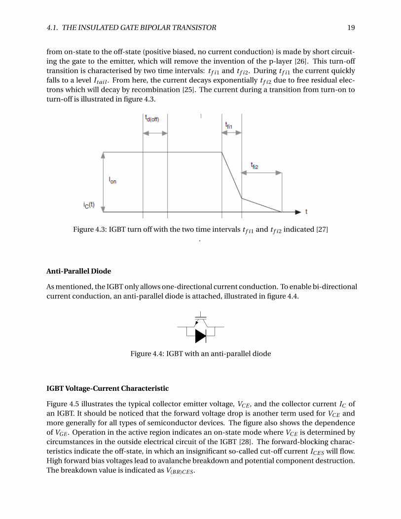
from on-state to the off-state (positive biased, no current conduction) is made by short circuit-ing the gate to the emitter, which will remove the invention of the p-layer [26]. This turn-offtransition is characterised by two time intervals: t f i 1 and t f i 2. During t f i 1 the current quicklyfalls to a level It ai l . From here, the current decays exponentially t f i 2 due to free residual elec-trons which will decay by recombination [25]. The current during a transition from turn-on toturn-off is illustrated in figure 4.3.
Figure 4.3: IGBT turn off with the two time intervals t f i 1 and t f i 2 indicated [27].
Anti-Parallel Diode
As mentioned, the IGBT only allows one-directional current conduction. To enable bi-directionalcurrent conduction, an anti-parallel diode is attached, illustrated in figure 4.4.
Figure 4.4: IGBT with an anti-parallel diode
IGBT Voltage-Current Characteristic
Figure 4.5 illustrates the typical collector emitter voltage, VC E , and the collector current IC ofan IGBT. It should be noticed that the forward voltage drop is another term used for VC E andmore generally for all types of semiconductor devices. The figure also shows the dependenceof VGE . Operation in the active region indicates an on-state mode where VC E is determined bycircumstances in the outside electrical circuit of the IGBT [28]. The forward-blocking charac-teristics indicate the off-state, in which an insignificant so-called cut-off current IC ES will flow.High forward bias voltages lead to avalanche breakdown and potential component destruction.The breakdown value is indicated as V(BR)C ES .
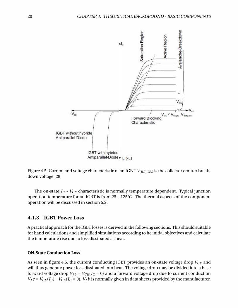
20 CHAPTER 4. THEORETICAL BACKGROUND - BASIC COMPONENTS
Figure 4.5: Current and voltage characteristic of an IGBT. V(BR)C ES is the collector emitter break-down voltage [28]
The on-state IC - VC E characteristic is normally temperature dependent. Typical junctionoperation temperature for an IGBT is from 25−125°C . The thermal aspects of the componentoperation will be discussed in section 5.2.
4.1.3 IGBT Power Loss
A practical approach for the IGBT losses is derived in the following sections. This should suitablefor hand calculations and simplified simulations according to he initial objectives and calculatethe temperature rise due to loss dissipated as heat.
ON-State Conduction Loss
As seen in figure 4.5, the current conducting IGBT provides an on-state voltage drop VC E andwill thus generate power loss dissipated into heat. The voltage drop may be divided into a baseforward voltage drop V f b = VC E (IC = 0) and a forward voltage drop due to current conductionV f c =VC E (IC )−VC E (IC = 0). V f b is normally given in data sheets provided by the manufacturer.
4.1. THE INSULATED GATE BIPOLAR TRANSISTOR 21
Accordingly, the power loss may be described as:
Pl oss = (V f c +V f b)IC (4.1)
The on-state power loss may be described by resistive electrical properties. Transconductancegm is defined in [24] as the change the collector current, IC , with respect to the collector-emittervoltage VC E :
gm = ∂IC
∂VC E(4.2)
Partial differentials are employed in equation 4.2, since the variables have other dependenciese.g. temperature. A linear relation between the VC E and IC may also be assumed, provided thatVGE is kept constant, the IGBT not operating in the active region and with a constant componenttemperature. This may described by a constant transconductance gm . The on-state power lossPloss can thus be expressed as:
Ploss = (V f b +IC
gm)IC (4.3)
1/gm is in some literature and simulation applications such as PSCAD referred to as the ON-stateresistance RON . The switching operations of the IGBT provide additional power loss. During aturn-OFF interval the voltage rises and current will decrease simultaneously and generate powerloss as:
Wswi chi ng loss =∫ t2
t1VC E IC d t (4.4)
Where t1 is the time when switching interval starts, and t2 is the time when the switching in-terval ends. Typical values are including switching times are specified in the manufacture datasheet.
4.1.4 IGBT ratings
In this section some of the parameters rated provided in data sheet for the IGBT is presented, asthese values are assumed essential for DC breaker design and simulation studies. The parame-ters and physics regarding IGBT temperature is discussed in section 5.2.
Rated collector emitter voltage VC Emax Maximum permissible voltage over collector-emitterterminals at module case temperatureTc = 25 °C.
Maximum power dissipation Ptot
Rated collector current IC max Maximum permissible continuous DC current based on the to-tal power dissipation.
Repetetive peak current ICr m Maximum current magnitude exceeding IC max for a specifiedamount of time.

22 CHAPTER 4. THEORETICAL BACKGROUND - BASIC COMPONENTS
4.2 Metal Oxide Varistor
The Metal Oxide Varistor (MOV) is a non-linear resistor consisting of zinc oxide elements (ZnO)that is normally used for protection applications from low voltage circuits to high voltage powerapparatus in which the MOV protects from lightning surges and other overvoltages. In a DCbreaker, the MOV may be an essential component for protecting the IGBT from overvoltagessuch as the TIV, providing the counter-voltage and dissipating the magnetic energy stored inthe line inductance. In terms of over-voltages a snubber circuit may also provide protectiondiscussed in section 5.1.1.
4.2.1 MOV Structure
The MOV is consist of ceramic microstructures of ZnO grains coated by an intergranular bound-ary containing other oxides. A typical ZnO grain diameter size indicated by d in figure 4.6 istypically 10− 100 µm while the intergranular boundary thickness t is typically 0.01− 0.1 µm.For low electric field strength, the MOV elements is highly resistive. However, when exposedto high electric fields it becomes highly conductive. The physical dimensions og the MOV de-termines the ratings. The capability of voltage is reflected in the length, and the capability tohandle currents in the cross sectional area. Thus the absorbing energy capacity is determinedby the volume. The MOV is normally capsuled with an insulating barrier [29, 30, 31].
Figure 4.6: Idealized structure of an MOV where d is the diameter of the ZnO grains and t is thethickness of the intergranular region [29]

4.2. METAL OXIDE VARISTOR 23
4.2.2 MOV Voltage-Current Characteristic
Ele
ctri
c fi
eld s
tren
gth
[V
/mm
]
2Current density [A/cm ]
Figure 4.7: Typical voltage-current characteristic of a ZnO MOV with the temperature depen-dency in the leakage current region, and the older silicon carbide (SiC) surge arrester character-istic also indicated [32].
The combination of the highly conductive ZnO grains an the more resistive intergranularboundary provides a voltage-current characteristic beneficial for overvoltage protection as de-picted in figure 4.7. The voltage-current characteristic is divided into three regions [31]:
1. The leakage current region
2. The protective region
3. The linear region
The interfaces of the regions may be gradual. The leakage current region in figure 4.7 may in thiscase be assumed to be in the range of 10−7−10−5 A/cm2 and provides very small currents, relatedto the high resistivity of the inter granular boundary. In the normal operating region, which inthis case can be assumed to 10−5 −102 A/cm2, a clear non-linear characteristic is observed. Ahigh rise in the current will provide only a marginal increase in voltage. This effect is associatedwith the electron tunnelling phenomenon. In the linear region with higher current density from102 A/cm2 and upwards, the characteristic tends more to linear resistive properties. The leak-age current region also has an unfavourable negative temperature coefficient, meaning that anincreased MOV-temperature provides higher leakage currents at a given voltage [30]. The VI-characteristics of a given type of an MOV may vary due to minor manufacture fluctuations. A 10% tolerance band in the voltage at given current should be expected according to [31].
4.2.3 MOV Equivalent Circuit and Equations
The VI characteristic may be expressed as:
IMOV = KMOV V αMOV (4.5)

24 CHAPTER 4. THEORETICAL BACKGROUND - BASIC COMPONENTS
Where KMOV is the ceramic material constant and α is the non-linearity exponent dependenton the operating region of the MOV. In the linear region α = 1, and in the non-linear regionα is determined by the VI-characteristic of the component, and can be found by logarithmiccalculations. If a constant MOV-voltage is assumed, the energy dissipated by the MOV duringfault clearance may be expressed by as:
WMOV =V α+1MOV KMOV tbr eak (4.6)
Where tbr eak is the break time of the DC breaker, the time interval between the DC breaker trips(peak line current) and the line current Il i ne is zero. If other resistive elements in the DC breakerand in the DC system are neglected, the DC breaker should be able to dissipate energy equal tomagnetic energy stored in the DC line and fed by the source during the fault clearance similarto equation 3.9.Figure 4.8 depicts an simple equivalent circuit of the MOV [31]. More detailed models can befound in [33]. Besides the non-linear property, the MOV also has dielectric properties reflectedin CMOV and a certain stray inductance LMOV due to the geometry of the current path. A variableresistor RMOV corresponds to the non-linear resistive property.
U
RMOVCMOV
LMOV
Figure 4.8: MOV equivalent ciruit
4.2.4 MOV Thermal Considerations and De-rating
The energy absorbed by the MOV will be dissipated as heat. If the electrical power losses are big-ger than heat dissipation, thermal instability may occur. Thermal instability involves deteriora-tion of the protection capabilities and eventually permanent component failure du to damageof the ZnO materials [30, 34]. Figure 4.9 illustrates this effect. For operating temperatures typ-ically higher than 85 °C , the MOV operating conditions in terms of voltage, surge current, andenergy absorption will de-rate [31]. This temperature is also referred to the critical temperature.
The handling of energy absorption is divided into two categories: Single impulse handlingcapability and thermal energy handling capability. The former relates to the sudden extremeincrease in temperature experienced by an MOV under current surges e.g. fault current andlightning impulses. This sudden temperature rise may lead to damages such as cracks in theZnO material. The latter thermal energy handling capability, is related to thermal instabilitywhich is more associated e.g. continuous electrical stresses and ageing [35].

4.2. METAL OXIDE VARISTOR 25
The performance of the MOV will de-rate under other circumstances such as repetitive surgesand the number of surges handled by the MOV in a long term perspective. The impact of de-rating due to temperature and current surges are normally provided in data sheets from themanufacturer.
Figure 4.9: Illustration of thermal stability of an MOV[34]
4.2.5 MOV Ratings
The MOV has the following ratings that should be considered for the DC-breaker design. Theratings listed are collected from [30, 31]
Operating voltage VMOV The voltage level (AC or DC) of the MOV that should only be exceededby transients - hence the maximum permissible voltage under normal operation.
Varistor voltage VV The voltage level of the MOV with 1m A applied .
Maximum energy dissipation WMOV max The maxium amount of energy dissipated over a pe-riod of 2 ms.
Maximum avarage power PMOV max The maxium power dissipation if the MOV has sufficienttime to cool between the surges.
Protection level/Clamping voltage Vc The voltage level of the MOV with currents higher than1m A applied.
Critical temperature Tcr i t i cal For temperature exceeding this level de-ratings of the MOV ap-plies.

26 CHAPTER 4. THEORETICAL BACKGROUND - BASIC COMPONENTS

Chapter 5
Theroretical Background - System Aspects
5.1 Stray inductance and Snubber Circuits
5.1.1 Stray Indcutance
Stray inductance Lσ is the unwanted inductive contribution in the commutations circuit to tran-sient overvoltages occurring during a semiconductor turn-off. For a DC breaker, this means theIGBT turn-off. According to [36], the stray inductance is expressed as:
Lσ =−∆VC Ed t
d IC(5.1)
Where ∆VC E is the additional voltage rise over the collector emitter terminals, and d t/d IC ,in this case, the inverse of the slope of the falling collector current when the semiconductorswitches off. An example of an idealised turn-off with stray inductance is shown in figure 5.1.It should be distinguished between the transient overvoltage contribution from Ll i ne referred toas TIV and the contribution from Lσ referred to as∆VC E . Lσ as mentioned unwanted inductancein the commutation circuit and is provided e.g. by the arrangement of the connected wires andgeometry of the electrical connections to the components.
5.1.2 Snubber Circuit
A snubber circuit is a parallel branch attached to the semiconductor with the intention of re-ducing stresses on the component during turn-on and turn-off. During turn-off, transient over-voltages may induced over the component due to stray inducances. For a DC breaker, a parallelcapacitor may protect the IGBT from transient overvoltages exceeding VC Emax and thus avoidcomponent failure [37]. The snubber may be realized with a capacitor only, or as a RCD snubberconsisting of a diode and a resistor in addition to the capacitor. The snubber should be placedas close possible the protected component as seen in figure 5.2. This will both reduce the strayinductance in the snubber circuit itself and protect the device from the transient over voltagecontributions from stray inductances. The energy stored in the snubber capacitor for after aswitching operation can be expressed as:
WC snub = 1
2CsnubV 2
C E (5.2)
27

28 CHAPTER 5. THERORETICAL BACKGROUND - SYSTEM ASPECTS
CΕ
V [
V]
an
d I
[A
]C
[ s]Time
Figure 5.1: Idealised IGBT turn-off transient due to stray inductance[36]
Lσ
Csnub
Figure 5.2: IGBT with free-wheeling diode, capacitor snubber circuit Csnub and stray inductanceLσ
For a solid state DC breaker using an additional small disk MOV replacing the capacitor snubberin figure 5.2 is also suggested [38]. This MOV may protect the IGBT from transient overvoltages,but without being the major contribution to dissipate the energy in system seen in equation 3.9.
5.2 Thermal Design Considerations
The performance power of semiconductors depends on the temperature of the device. Whenthe component junction temperature T j , referred the intrinsic temperature, surpasses a cer-tain level, the characteristics of the device are lost and may lead to failure. In the componentdata sheets the manufacturer specifies the maximum junction temperature T j max . By practicalmeans, the power loss will increase with the junction temperature, as a self amplifying pro-

5.2. THERMAL DESIGN CONSIDERATIONS 29
cess as temperature will increase even further. Higher junction-temperature may also reducereliability of the component [25]. Thermal considerations normally includes to determine anadequate heat sink and cooling medium to conduct the heat away from the component in orderto maintain the junction temperature below T j max . In the following sections simplified circuitmodels is described intended to emulate the dynamics and steady-state characteristics of heattransfer and temperature in semiconductors devices. For simplification only one dimensionalheat transfer is considered.
5.2.1 Thermal Resistance
The energy flow or conducted heat Pcond per unit time through a section of material may beexpressed as:
Pcond = λA∆T
d(5.3)
Where λ [W /m ·C °] is the thermal conductivity , ∆T [°C ] is the temperature difference acrossthe material , d is the length [m] and A [m2] the cross-section area.From equation 5.3 the thermal resistance Rθ [W /C °] can be defined as:
Rθ =∆T
Pcond= d
λA(5.4)
Rθ for a given semiconductor is normally provided in data sheets, with typically different valuesfor the layers of the device which in sum may determine the steady-state thermal impedancefrom the junction to the case surface of the component.
5.2.2 Thermal Capacitance
To obtain an emulation of the dynamic behaviour a thermal capacitance Cθ analogous to elec-trical capacitance is considered. Thermal transients must be considered when switching, andhaving rapid changes in currents. This may generate additional heat to the steady state on-statelosses. DC grid faults may also provide fast a changing current and additional power loss. Thedynamics is related to the thermal heat capacity Cv , which is defined by the change of heat dQwith respect to the temperature change dT . For a square shaped box of an arbitrary materialthe heat capacity Cv is defined as:
Cv = dQ
dTAd (5.5)
5.2.3 Thermal Equivalent Electrical Circiut
The time response is simplified into one dimensional heat conduction which includes exponen-tial behaviour with thermal time constants [25]. The exponential behaviour may be modelledas an electrical RC network intended to emulate both the steady state and the dynamic temper-ature response. The power dissipated in the semiconductor P (t ) is reflected as the current inthe network and the temperature as the voltage. An example of a network is shown in figure 5.3referred to as the Cauer electro thermal model. The voltage T1(t )-Ta represents the temperaturedifference between layer 1 and the ambient temperature. Layer 1 typically represents the junc-tion in a semiconductor-device. The Cauer model represents a physical approach to transient

30 CHAPTER 5. THERORETICAL BACKGROUND - SYSTEM ASPECTS
T1(t )Rθ1 Rθ2 Rθi
P (t ) C ′θ1 C ′
θ2 C ′θi
Ta
Figure 5.3: Cauer electro thermal model
thermal equivalent impedance, but provides complex calculations to obtain the time constantsfor each layer [39, 40]. A mathematically simpler model, The Foster model, may be used forthermal calculation instead. This model represents each layer with a time constant and emu-lates the a time dependent transient thermal-impedance Zθ j c (t ). Figure 5.4 depicts an exampleof the Foster model. The thermal transient may be fitted into an exponential curve obtained in[39], expressed as:
Zθ j c (t ) =n∑
i=1Rθi (1−e
−t
τθi ) (5.6)
Where τθi is thermal time constant for the respective layers. The Foster model does howevernot represents the physical layers along the heat conduction path. The circuit parameters in theFoster model are normally given in data sheet as τθi and Rθi . Cθi is calculated by:
τθi = Rθi Cθi (5.7)
T1(t )Rθ1 Rθ2 Rθi
P (t )
Ta
Cθ1 Cθ2 Cθi
Figure 5.4: Foster electro thermal model
5.3 Heat sinks, Thermal Grease and Cooling Medium
The purpose of using a heat sink is to provide a low thermal resistance heat conduction pathbetween the cooling medium or ambient air and the semiconductor. I.e. is to conduct heataway from the device and maintaining an acceptable component temperature. As seen the inequation 5.3, the heat power loss is conducted to the surroundings by keeping the distance ofheat conduction d small and the cross sectional area of the material A big as possible. Theheat sink should therefore maximise its surface area, but provide a small path for the heat con-duction. Efficient heat-conduction is dependent on the movement of the ambient air or the
5.3. HEAT SINKS, THERMAL GREASE AND COOLING MEDIUM 31
cooling medium. Standstill air may result in increasing surrounding temperature, and thusincreasing component temperature as Rθheat si nk is expected to be higher. Auxiliary fans at-tached to the heat sink may contribute to mitigate this effect. Heat sinks have time constantsτheat si nk = 4−15 mi n typically [25].
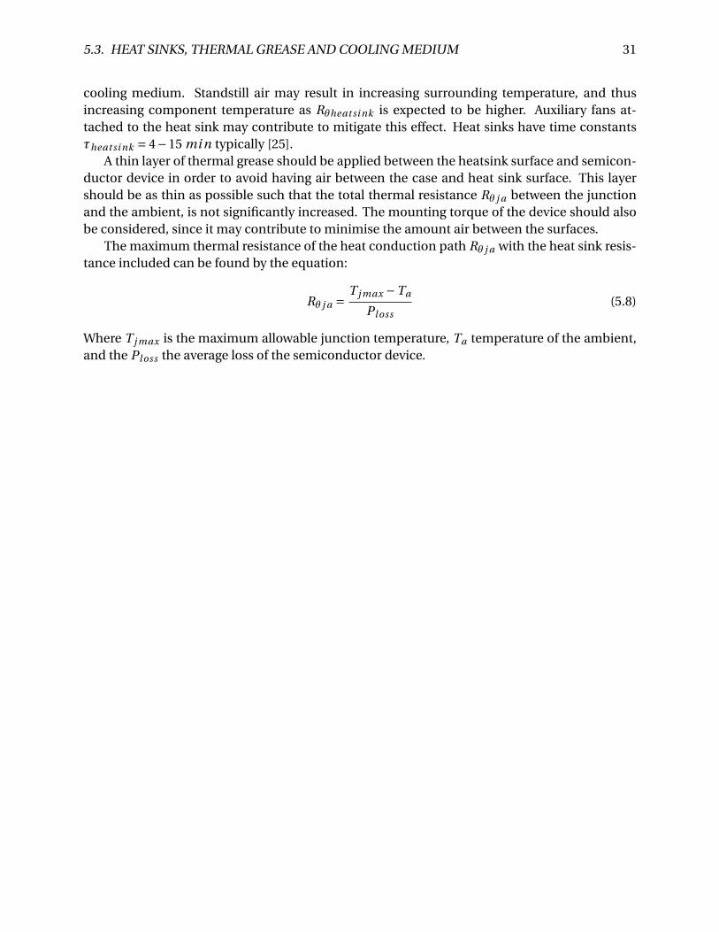
A thin layer of thermal grease should be applied between the heatsink surface and semicon-ductor device in order to avoid having air between the case and heat sink surface. This layershould be as thin as possible such that the total thermal resistance Rθ j a between the junctionand the ambient, is not significantly increased. The mounting torque of the device should alsobe considered, since it may contribute to minimise the amount air between the surfaces.
The maximum thermal resistance of the heat conduction path Rθ j a with the heat sink resis-tance included can be found by the equation:
Rθ j a = T j max −Ta
Ploss(5.8)
Where T j max is the maximum allowable junction temperature, Ta temperature of the ambient,and the Pl oss the average loss of the semiconductor device.

32 CHAPTER 5. THERORETICAL BACKGROUND - SYSTEM ASPECTS

Chapter 6
Considerations and Description ofLaboratory Work
This chapters introduces the NTNU/SINTEF Smart Grid and Renewable Energy Lab including aDC grid, for which the final DC breaker should be designed for. A DC breaker test model used inthe design process and a test of a contactor switch is described as well.
6.1 NTNU/SINTEF Smart Grid and Renewable Energy Lab
The NTNU/SINTEF Smart Grid and Renewable Energy Lab is a power system infrastructure builtfor research related to smart grids and renewable energy generation. The laboratory will furtherbe referred to as the NTNU/SINTEF lab. The NTNU/SINTEF lab consist of different parts includ-ing an induction generator, a distribution grid and a DC grid consisting of four interconnected60 kVA voltage source converters (VSC) intended to emulate a HVDC transmission system. Thefollowing section describes the details needed for the DC breaker design. A more detailed de-scription of the laboratory is found in [41, 42].
6.1.1 The 60 kVA Converter
Figure 6.1 shows the configuration of the three main parts. The three main parts of the converterare:
Converter module: IGBT brigdes and DC-link capacitor
Harmonics filter: LCL-type filter
Switchgear: Contactor, charging and discharge circuit.
The converter and the DC grid model has the following rated values:
Rated DC-voltage: 0-750 V
Rated current: 0-100 A
DC-link capacitor bank: 12 · 4700 µF = 56.4 mF
33
34 CHAPTER 6. CONSIDERATIONS AND DESCRIPTION OF LABORATORY WORK
IGBT modules: 400 A 1200 V IGBT module, 2 per phase
The DC-link capacitors must be charged by an external circuit before the converter can operate.The IGBT driver circuits are also equipped with overcurrent protection with an adjustable tip-range of 0−800 A. A technical detailed description of the VSC is given in [43].
AC
Filter
+DC -
Switchgear Converter
Figure 6.1: Main parts of the 60 kVA VSC for the DC grid in the NTNU/SINTEF lab [43]
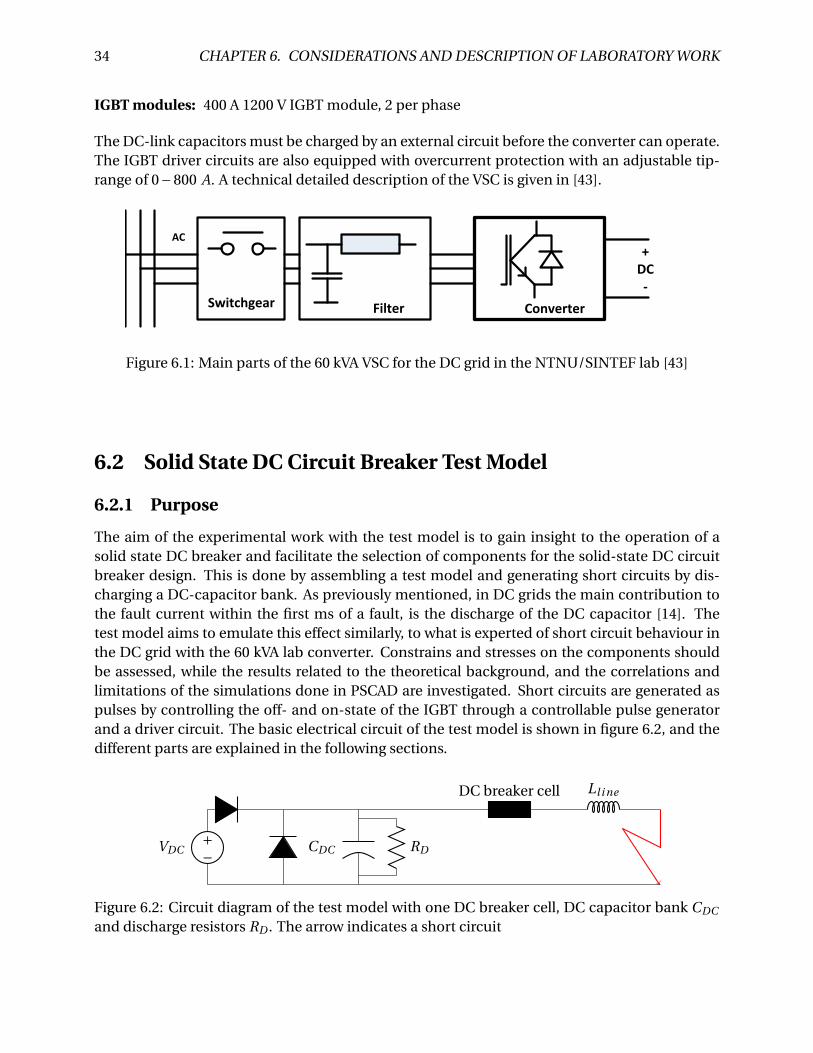
6.2 Solid State DC Circuit Breaker Test Model
6.2.1 Purpose
The aim of the experimental work with the test model is to gain insight to the operation of asolid state DC breaker and facilitate the selection of components for the solid-state DC circuitbreaker design. This is done by assembling a test model and generating short circuits by dis-charging a DC-capacitor bank. As previously mentioned, in DC grids the main contribution tothe fault current within the first ms of a fault, is the discharge of the DC capacitor [14]. Thetest model aims to emulate this effect similarly, to what is experted of short circuit behaviour inthe DC grid with the 60 kVA lab converter. Constrains and stresses on the components shouldbe assessed, while the results related to the theoretical background, and the correlations andlimitations of the simulations done in PSCAD are investigated. Short circuits are generated aspulses by controlling the off- and on-state of the IGBT through a controllable pulse generatorand a driver circuit. The basic electrical circuit of the test model is shown in figure 6.2, and thedifferent parts are explained in the following sections.
+−VDC
DC breaker cell Ll i ne
CDC RD
Figure 6.2: Circuit diagram of the test model with one DC breaker cell, DC capacitor bank CDC
and discharge resistors RD . The arrow indicates a short circuit

6.2. SOLID STATE DC CIRCUIT BREAKER TEST MODEL 35
6.2.2 Voltage Source and DC Capacitor
The capacitor bank CDC consists of eight similar DC electrolytic capacitors of 4700 µF each andare arranged in parallel; in total CDC = 37.6 mF. The capacitor bank is shown in figure 6.3. It ischarged with a adjustable DC source VDC = 0−300 V with a current limitation of 1 A. The useof the DC source is beneficial since it can be connected to the 230 V supply. Blocking diodesare connected in series with the positive pole of the voltage source VDC and in parallel with thecapacitor CDC . This is to protect the capacitor bank and the voltage source from high inrushcurrents during short circuits. For safety reasons, 8 high ohmic discharge resistors of RD =47 kΩeach, are connected in parallel with the 8 capacitors. The resistors dissipate the stored energyand ensure 0 V capacitor terminal voltage when not in use.
Figure 6.3: Test model capacitor bank CDC
6.2.3 Solid State DC Circuit Breaker
Configuration
Figure 6.4 depicts the configuration of the DC breaker, and figure 6.5 shows the set up. The IG-BTs used are SIEMENS Single switch IGBT Power Modules with free-wheeling diodes. The rat-ings are listed in table 6.1. The data-sheet is attached in appendix A. For the basic configurationin figure 6.4, an MOV is connected in parallel with a set of the SIEMENS IGBT modules in anti-series according to the solid state DC breaker topology. The MOV types used in the experiments

36 CHAPTER 6. CONSIDERATIONS AND DESCRIPTION OF LABORATORY WORK
are EPCOS high-energy varistors and are listed in table 6.2. The MOV indicated in figure 6.4 isnamed Energy MOV, as it is mainly used for energy dissipation in the experiments related to thetest model. Transient overvoltage suppression due to stray inductances is provided by solutionswhich will be explained in chapter 8. The IGBTs in anti-series are named A− and A+, since thecontrol system originally is design for a 3-phase converter.
U
Energy MOV
IGBT A+
IGBT A-
Figure 6.4: Basic configuration circuit diagram of the DC breaker in the test model
Figure 6.5: Basic configuration of the DC breaker in the test model
Table 6.1: Ratings for SIEMENS SM 300 GA 120 DN2 Single switch IGBT module
SIEMENS Single Swith IGBTVC Emax 1200 VIC max 430 A (DC)
6.2. SOLID STATE DC CIRCUIT BREAKER TEST MODEL 37
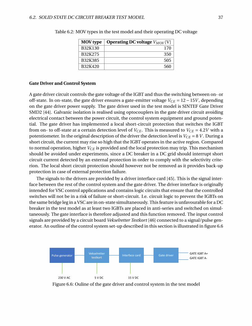
Table 6.2: MOV types in the test model and their operating DC voltage
MOV type Operating DC voltage VMOV [V]B32K130 170B32K275 350B32K385 505B32K420 560
Gate Driver and Control System
A gate driver circuit controls the gate voltage of the IGBT and thus the switching between on- oroff-state. In on-state, the gate driver ensures a gate-emitter voltage VC E = 12−15V , dependingon the gate driver power supply. The gate driver used in the test model is SINTEF Gate DriverSMD2 [44]. Galvanic isolation is realised using optocouplers in the gate driver circuit avoidingelectrical contact between the power circuit, the control system equipment and ground poten-tial. The gate driver has implemented a local short-circuit protection that switches the IGBTfrom on- to off-state at a certain detection level of VC E . This is measured to VC E = 4.2V with apotentiometer. In the original description of the driver the detection level is VC E = 8 V . During ashort circuit, the current may rise so high that the IGBT operates in the active region. Comparedto normal operation, higher VC E is provided and the local protection may trip. This mechanismshould be avoided under experiments, since a DC breaker in a DC grid should interrupt shortcircuit current detected by an external protection in order to comply with the selectivity crite-rion. The local short circuit protection should however not be removed as it provides back-upprotection in case of external protection failure.
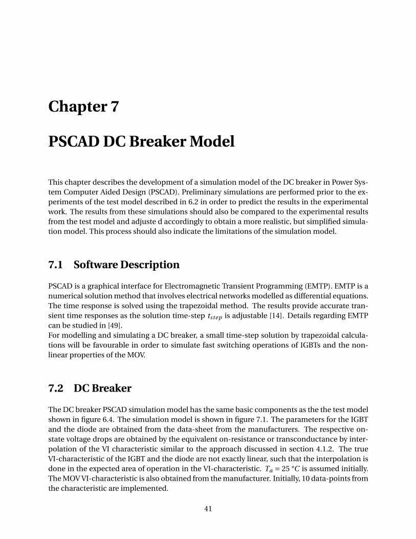
The signals to the drivers are provided by a driver interface card [45]. This is the signal inter-face between the rest of the control system and the gate driver. The driver interface is originallyintended for VSC control applications and contains logic circuits that ensure that the controlledswitches will not be in a risk of failure or short-circuit. I.e. circuit logic to prevent the IGBTs onthe same bridge leg in a VSC are in on-state simultaneously. This feature is unfavourable for a DCbreaker in the test model as at least two IGBTs are placed in anti-series and switched on simul-taneously. The gate interface is therefore adjusted and this function removed. The input controlsignals are provided by a circuit board Vekselretter Testkort [46] connected to a signal/pulse gen-erator. An outline of the control system set-up described in this section is illustrated in figure 6.6
Pulse generator Interface cardVekselretter
testkortGate driver
GATE IGBT A+
GATE IGBT A-
230 V AC 5 V DC 15 V DC
Figure 6.6: Ouline of the gate driver and control system in the test model

38 CHAPTER 6. CONSIDERATIONS AND DESCRIPTION OF LABORATORY WORK
6.2.4 Inductive Element
The inductance Ll i ne , indicated in figure 6.2, represents an inductive property in a DC line ora cable. The inductance should be varied as faults may occur on different locations a DC-grid.Low inductances may represents short circuits near the converter stations, and the higher value,the further fault distance from the converter station. Linear inductors are used, such that theinductance is not affected by the magnitude of the current. The inductances used are listed intable 6.3
Table 6.3: Inductors used in the lab test model
Inductor Inductance [µH]L1 44.5L2 119.5L3 1091.6
6.2.5 Measurement Technique
In order to capture the voltage and current waveforms a TEKTRONIX TDS 2014 oscilloscopeis used. The current is measured via a current clamp meter, LEM sensors and a Rogowski coil.The voltage is measured with differential probes and provides galvanic isolation to avoid groundpotential contact. A temperature transducer is also used for measuring the surface temperatureof the components and connected to an Agilent LXI data acquisition unit.
6.2.6 Limitations
The test model described will have some limitations. Relevant correlations for the DC breakerdesign for the NTNU/SINTEF lab as well as a full scale DC grid may not be tested. The testmodel has no load and only short circuits are generated, meaning that the on-state losses undernormal operation (non-fault state) cannot be investigated. Thus heating of the semiconductorsand the MOVs under the mentioned circumstances cannot be investigated directly. There isalso no protection system, and the durations of the short circuits are manually controlled by theVekselretter Testkort and the signal generator. A contactor switch is not included in the set-upof the test model. And therefore the interaction between this component and remaining cannotbe tested directly.
6.3 Contactor Switch Test
Physical isolation is needed after the DC breaker has forced the current to zero in a DC grid.This is to provide a separation of the faulted parts from the healthy parts in the power system.For the DC breaker in the NTNU/SINTEF lab, a contactor switch in series with the DC breaker issuggested for this application. Therefore some testing of this device will be undertaken.
The contactor should be able to isolate and break eventual residual current that may oc-cur after the DC breaker has forced the short circuit current to zero. The contactor will be in

6.3. CONTACTOR SWITCH TEST 39
the series with Ll i ne and will thus interrupt residual inductive current. As seen in the theo-retical background section 3.1 this may be problematic as the inductance will try to maintaina constant flux and induce high voltages if the current is interrupted. An experimental test isundertaken in order to investigate the behaviour of the contactor switch under the mentionedcircumstances. The purpose of this test is to provide predictions of the operation of a contactorswitch for isolator applications in relation with a solid state DC breaker. The set up of the test isshown in 6.7 A contactor switch for DC applictations of type KILOVAC EV200 [47] is tested with
+−VDC
Rl oad Ll oad
Contactor switch
Figure 6.7: Contactor switch test circuit
an inductive load Lload = 117 mH, an adjustable resistor Rl oad controls the current and a voltagesource VDC = 300 V. The test circuit seen in figure 6.7. The switches is controlled by a DC supplyVcoi l , providing voltage to a coil energising an electromagnet inside the contactor switch hous-ing. When the supply is switched on, i.e Vcoi l = 24 V, current conducts freely through the maincontacts. When the supply is switched off, i.e. Vcoi l = 0 V, the switch is isolating as the electro-magnet is demagnetised. The contactor switch also has auxiliary contacts which are open whenthe contactor is open. The voltage of the auxiliary contacts is referred to as Vaux . These con-tacts may be used to provide signals to the control system. The detailed electromagnetic andmechanical operation the structure of a DC contactor switch can be studied in [48].

40 CHAPTER 6. CONSIDERATIONS AND DESCRIPTION OF LABORATORY WORK
Chapter 7
PSCAD DC Breaker Model
This chapter describes the development of a simulation model of the DC breaker in Power Sys-tem Computer Aided Design (PSCAD). Preliminary simulations are performed prior to the ex-periments of the test model described in 6.2 in order to predict the results in the experimentalwork. The results from these simulations should also be compared to the experimental resultsfrom the test model and adjuste d accordingly to obtain a more realistic, but simplified simula-tion model. This process should also indicate the limitations of the simulation model.
7.1 Software Description
PSCAD is a graphical interface for Electromagnetic Transient Programming (EMTP). EMTP is anumerical solution method that involves electrical networks modelled as differential equations.The time response is solved using the trapezoidal method. The results provide accurate tran-sient time responses as the solution time-step tstep is adjustable [14]. Details regarding EMTPcan be studied in [49].For modelling and simulating a DC breaker, a small time-step solution by trapezoidal calcula-tions will be favourable in order to simulate fast switching operations of IGBTs and the non-linear properties of the MOV.
7.2 DC Breaker
The DC breaker PSCAD simulation model has the same basic components as the the test modelshown in figure 6.4. The simulation model is shown in figure 7.1. The parameters for the IGBTand the diode are obtained from the data-sheet from the manufacturers. The respective on-state voltage drops are obtained by the equivalent on-resistance or transconductance by inter-polation of the VI characteristic similar to the approach discussed in section 4.1.2. The trueVI-characteristic of the IGBT and the diode are not exactly linear, such that the interpolation isdone in the expected area of operation in the VI-characteristic. Ta = 25 °C is assumed initially.The MOV VI-characteristic is also obtained from the manufacturer. Initially, 10 data-points fromthe characteristic are implemented.
41

42 CHAPTER 7. PSCAD DC BREAKER MODEL
Figure 7.1: Basic DC breaker model in PSCAD
7.3 DC Grid
7.3.1 DC Line
The DC line model is modelled with an inductor and a resistor in series. There are existingmore complicated frequency dependent models for overhead lines (OHL) and cables in PSCADsuitable for full scale system simulations as described in [49]. For both the test model and asa starting point for the DC grid in the NTNU/SINTEF lab a simple configuration shown in fig-ure 7.2 is used. In the preliminary simulations the resistor is set to zero since there is only aninductor in the test model, as seen in figure 6.2. The internal resistance in the inductor and thewires are assumed to be insignificant in the preliminary simulations.
Figure 7.2: DC line model in PSCAD
7.3.2 Voltage Source, Capacitor and Load
For simulations of the test model the voltage source and the DC capacitor bank is implementedas shown in figure 7.3. The Ideal breakers, indicated as BRK1 and BRK2, control the charging anddischarging of the capacitor bank. No load is implemented since only short circuits are gener-ated as seen in figure 6.2. The discharging resistor RD is omitted in the simulation model due itsto high time-constant value compared to the duration of the short circuit. As a simplification,theNTNU/SINTEF lab DC grid converter is implemented as a single voltage source. Implementa-tion of a real VSC model would require more complicated models including a converter controlsystem. Similar simplification has been done in [14, 50]. The load in the NTNU/SINTEF lab DC

7.4. OVERCURRENT PROTECTION 43
Figure 7.3: Test model capacitor and voltage source in PSCAD
grid PSCAD model is implemented as a controllable voltage source and set to zero when a shortcircuit is simulated.
7.4 Overcurrent Protection
A protection system is assumed for the NTNU/SINTEF lab DC grid. The selected approach inPSCAD is to implement a simple overcurrent protection. This is done by simple logics, in thiscase a J-K latch, witch is trigged by a signal comparator when the line current exceeding a spec-ified magnitude. The protection system response time tr esponse is emulated via a time delayfunction.The PSCAD overcurrent protection implemented is shown in figure 7.4. The interpo-lation capability in PSCAD is used, and therefore the J-K latch needs two signals for each input.
Figure 7.4: Protection system model in PSCAD with line current comparator, the J-K latch, andthe time delay function
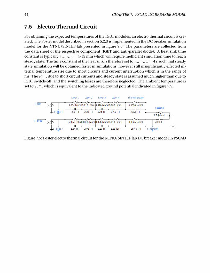
44 CHAPTER 7. PSCAD DC BREAKER MODEL
7.5 Electro Thermal Circuit
For obtaining the expected temperatures of the IGBT modules, an electro thermal circuit is cre-ated. The Foster model described in section 5.2.3 is implemented in the DC breaker simulationmodel for the NTNU/SINTEF lab presented in figure 7.5. The parameters are collected fromthe data sheet of the respective component (IGBT and anti-parallel diode). A heat sink timeconstant is typically τheat si nk =4-15 min which will require inefficient simulation time to reachsteady state. The time constant of the heat sink is therefore set to τheat si nk = 4 s such that steadystate simulation will be obtained faster in simulations, however still insignificantly effected in-ternal temperature rise due to short circuits and current interruption which is in the range ofms. The Ploss due to short circuit currents and steady state is assumed much higher than due toIGBT switch-off, and the switching losses are therefore neglected. The ambient temperature isset to 25 °C which is equivalent to the indicated ground potential indicated in figure 7.5.
Figure 7.5: Foster electro thermal circuit for the NTNU/SINTEF lab DC breaker model in PSCAD

Chapter 8
Results
This chapter presents the main results from laboratory work with the DC breaker test modeldescribed in section 6.2 including a comparison with the preliminary simulations in PSCAD.Thereafter the PSCAD model is adjusted to match the experimental work in order to obtain amore realistic DC breaker model. The results from testing of the contactor switch described insection 6.3 is also presented. All results are processed in and plotted with MATLAB.
8.1 Objective of Results Analysis
Before presenting the results a brief discussion is carried out in order to determine what valuesare of interest and hence should be obtained from the experimental work.
The peak value of IGBT A+ voltage, peak VC E , is examined as it may exceed the VC Emax . Thepeak line current Il i ne should also be included. As seen in section 3.1.2 and 5.1.1, the highercurrents interrupted, the higher transient overvoltages provided. The peak Il i ne may also be anindication on the stresses due to different fault currents interrupted. The energy dissipated inthe energy MOV per fault clearance WMOV and the instantaneous power PMOV of the energyMOV is of interest. These values should be within the maximum ratings of the component toprevent deteriorating temperature rises and eventually failure. The break time tbr eak is alsoobtained from the results, since a DC breaker should interrupt and force the fault current tozero in the shortest amount of time.
For the contactor switch, the voltage Vswi tch and the current Iswi tch should be measured asthese value provides the current breaking behaviour of the switch. The corresponding controlsignals is measured in the form the voltage over the electromagnetic coil Vcoi l and the auxiliarycontact Vaux .
Tables 8.1 and 8.2 present the values which will be obtained from the experimental work.Table 8.2 presents the values calculated in MATLAB.
8.2 Laboratory Test Model Results
This section presents the main results An overview of the test model operation principles ispresented initially followed by detailed analysis of different aspects of a DC breaker. The detailsof the test model set up is described in section 6.2.
45

46 CHAPTER 8. RESULTS
Table 8.1: Explaination of values measured
Symbol [unit] ExplanationIl i ne [A] Line currnetVl i ne [V] Line voltage, represented as the voltage over inductorVC E [V] Collector emeitter votage IGBT A+IMOV [A] Energy MOV currentVMOV [V] Energy MOV voltageTMOV [°C] Energy MOV temperatureVDCC B [V] Circuit breaker cell voltageIswi tch [A] Contactor switch currentVswi tch [V] Contactor switch voltageVcoi l [V] Contactor switch main coil voltageVaux [V] Contactor switch auxiliary contact voltage
Table 8.2: Explanation of values calculated
Symbol [unit] ExplanationPMOV [kW] Instantaneous power in the energy MOV , the product of VMOV and IMOV
WMOV [J]Dissipated energy in the energy MOV, time integral of PMOV
calculated with the trapezoidal method
tbr eak [ms]DC breaker break time,the time interval from peak line current to zero line current(Il i ne = 0 A)
IC [A] Collector current of the IGBT A+, IC = Il i ne − IMOV
tzer o [ms] Time interval from Vcoi l is set to 0 V to Iswi tch = 0 Vtaux [ms] Time interval from Vcoi l is set to 0 V to Vaux is open circuited
8.2.1 Principle of Operation
For showing principle of operation of the DC breaker test model, an initial experiment using theparameters listed in table 8.3 is undertaken.
Table 8.3: Parameter values in the initial experiment
Parameter ValueVDC 200 Vtpul se 1 msLl i ne 1091.6 µHEnergy MOV 350 V DC
Figure 8.1 shows the entire time period from the initiation of the short circuit to the short circuitclearance. When the IGBT A+ is switched to on-state, the voltage over Ll i ne , Vl i ne =VDC−VDCC B .VDCC B is the sum of the voltage drop over the IGBT A+ and the anti-parallel diode of IGBT A-.Seen in figure 8.1, Vl i ne can be assumed constant in the duration of the short circuit. A con-stant Vl i ne provides thus a constant positive slope of Il i ne similar to equation 3.3. After the shortcircuit duration of tpul se , the IGBT A+ switches off and commutates the current into the energy

8.2. LABORATORY TEST MODEL RESULTS 47
MOV. During this commutation seen in figure 8.2, two connected phenomena are observed: Thepeak voltage of IGBT A+ and the inrush current in the energy MOV. First the voltage rise over theIGBT and the initial inrush current to the varistor are observed. Due the fast change in current,the stray inductance contributes to an additional voltage rise ∆VC E , explained in the theoreti-cal background by equation 5.1. The traces of a damped oscillation in the waveform during thecommutation may be explained by an interaction between the stray inductance, parasitic ca-pacitances and the resistive property of the energy MOV. After the oscillations, the voltage overthe DC breaker VDCC B behaves similarly to the V-I characteristic of the MOV. In figure 8.1, it isobserved that VDCC B > VDC and thus Vl i ne < 0, according to the discussion with the countervoltage principle described in section 3.2. The counter voltage provides at this point a negativeslope of the Il i ne as long as Vl i ne < 0 is satisfied. When Il i ne approaches zero, the VDCC B dropsrapidly as the energy MOV now operates in the leakage current region. Eventually VDCC B =VDC .At this point, only residual leakage current from the MOV and IGBT module will flow. This cur-rent must be interrupted by an isolation switch such as a contactor to ensure complete shortcircuit clearance and physical isolation.
Time [ms]0 0.5 1 1.5 2 2.5
Curren
t[A
]
-250
-200
-150
-100
-50
0
50
100
150
200
Voltage[V
]
-1000
-800
-600
-400
-200
0
200
400
600
800
IlineVline
VDCCB
Figure 8.1: Interruption of a short circuit in the test model with VDC = 200 V, Ll i ne = 1091.6 µH,VMOV = 350 V and tpul se = 1 ms
8.2.2 Effect of Line Inductance
The purpose of the experiments discussed in this section is to investigate the effect a line in-ductance for the operation of a DC breaker and thus the implication of the fault location asdiscussed in section 6.2.4. The experiments are conducted with the fixed parameters listed in

48 CHAPTER 8. RESULTS
table 8.4. The inductance Ll i ne is varied between L1, L2 and L3, listed in table 6.3.
Table 8.4: Fixed parameters for the test with variation of line inductance Ll i ne
Parameter ValueVDC 50 Vtpul se 0.2 msEnergy MOV 170 V DC
Table 8.5: Results in the test with variation of line inductance Ll i ne
Ll i ne peak Il i ne [A] peak VC E [V] peak PMOV [kW] WMOV [J] tbr eak [ms]L1 = 44.5 µ H 249.02 316.00 27.07 0.485 0.030L2 = 119.5 µ H 78.43 282.00 13.50 0.230 0.033L3 = 1091.6 µ H 10.88 240.00 4.21 0.039 0.034
It can be observed from the results in table 8.5 that a smaller inductance provides a steeper slopeof the short circuit current, since the peak current is increasing with smaller Ll i ne for a constanttpul se . The results show some of the consequences of higher currents: A higher transient over-voltage ∆VC E due to stray inductances, and higher instantaneous power and energy dissipatedin the energy MOV as discussed in section 3.3. It can be seen that higher currents due to low
Time [µs]0 0.2 0.4 0.6 0.8 1
Curren
t[A
]
-100
0
100
200
300
400
500
600
Voltage[V
]
0
200
400
600
800
1000
1200
1400
ICIMOV
VCE
Figure 8.2: Commutation of Il i ne from the A+ IGBT into the energy MOV under a short circuitcurrent interruption VDC = 200V , Ll i ne = 1091.6 µH , VMOV = 350 V and tpul se = 1ms

8.2. LABORATORY TEST MODEL RESULTS 49
inductance contribute significantly more to the energy dissipated in the MOV than the induc-tance according to equation 3.9. The results also show an insignificant variation in tbr eak dueto the marginal change in the voltage of the energy MOV with the variation of the peak currentseen in the V-I characteristic in figure 4.7.
Inductance and Damping
The variation of inductance affects also the damping of oscillations after the energy MOV voltagehas dropped to zero. A smaller inductance, or a shorter DC line, also has lower resistance. Fig-ure 8.3 shows that the result is voltage oscillations with poorer damping compared to figure 8.1.It can be assumed that these oscillations are caused by capacitive properties in the DC breakersuch as parasitic capacitance of the IGBT modules and smaller line resistance. Besides voltageoscillations, small residual current oscillations are also observed. As mentioned a contactor issuggested to interrupt this current.
Time [ms]0 0.01 0.02 0.03 0.04 0.05 0.06 0.07 0.08 0.09 0.1
Curren
t[A
]
0
2
4
6
8
10
12
14
16
18
20
Voltage[V
]
-1000
-800
-600
-400
-200
0
200
400
600
800
1000
IlineVDCCB
Figure 8.3: Effect of damping, inductance and residual currents after short circuit clearance withVDC = 200V, Ll i ne = 45 µH , VMOV = 350 V and tpul se = 70µs
8.2.3 Effect of Detection Time
A protection system may have a certain response time or time delay from the fault detection tothe DC breaker trips. The effect of this delay is investigated in this section by varying the dura-tion of the short circuit, by means of adjusting the pulse length tpul se . The constant parametersused in the experiments are listed in table 8.6. The results presented in table 8.7 indicates that a

50 CHAPTER 8. RESULTS
Table 8.6: Fixed parameters in the test with variation of detection time or tpul se
Parameter ValueVDC 50 VLl i ne 1091.6 µHEnergy MOV 350 V DC
longer pulse time provides a higher current to interrupt for the DC breaker. As the source volt-age and inductance are constant, the rising short circuit current slope must be the same for alltpul se . The effect of higher currents is similar to the discussion in section 8.2.2: Higher peak VC E ,higher PMOV and higher WMOV . The undesirable effect of overvoltages due the stray inductanceis also clear in this case as VC E > VC Emax = 1200 V is observed. Since the line inductance isthe same for all tpul se , and the energy MOV voltage VMOV only changes marginally, the negativecurrent slope of Il i ne is approximately the same for all tpul se . This is also according to equa-tion 3.4 described in the theoretical background. Therefore, tbr eak increases with higher peakline current Il i ne being interrupted.
Table 8.7: Results from test with variation of detection time or tpul se
tpul se [ms] peak Il i ne [A] peak VC E [V] peak PMOV [kW] WMOV [J] tbr eak [ms]2 92.16 970.00 46.80 3.48 0.1434 170.59 1160.00 78.00 10.11 0.2576 235.29 1270.00 95.04 15.85 0.331
8.2.4 Effect of Source Voltage
As the voltage of a VSC in the NTNU/SINTEF lab may be varied, variation of the source voltageVDC of the test model is examined. The fixed parameters used in the experiments conducted inthis section are listed in table 8.8.
Table 8.8: Fixed parameters in the test with variation of VDC
Parameter ValueLl i ne 1091.6 µHtpul se 1 msEnergy MOV 350 V DC
The results listed in table 8.9 show that a higher source voltage VDC provides a higher currentslope. Thus a higher current is interrupted for the same duration of the short circuit. The effectsof higher Il i ne are similar to the results in section 8.2.2 and section 8.2.3 in terms of the corre-lation between higher currents and peak VC E , peak PMOV and WMOV . The break time tbr eak ishowever longer since a higher voltage VDC provides a smaller negative voltage drop over Ll i ne .

8.2. LABORATORY TEST MODEL RESULTS 51
Table 8.9: Results from the test with variation of VDC
VDC [V] peak Il i ne [A] peak VC E [V] peak PMOV [kW] WMOV [J] tbr eak [ms]100 98.03 970 23.76 2.318 0.160200 215.68 1240 51.68 12.60 0.434300 349.02 1370 67.20 32.18 0.902
8.2.5 Effect of Energy MOV
For the final DC breaker design, a suitable energy MOV should be determined. Therefore boththe effect of the rated MOV voltage and the heating, discussed in section 4.2.4, will be examined.
Variation of Energy MOV
The rated voltage of the energy MOV is varied, and fixed parameters used in this experiment arelisted in table 8.10. The results are shown in table 8.11.
Table 8.10: Fixed parameters in test with the variation of MOV
Parameter ValueVDC 200 Vtpul se 1 msLl i ne 1091.6 µH
The peak current varies insignificantly, due to constant Ll i ne , tpul se and VDC . The peak volt-age of VC E varies and increases with rising rated energy MOV voltage, and thus also provide anincreasing peak instantaneous power of the energy MOV. The break time tbr eak decreases andtherefore also WMOV decreases. This can be explained by a higher counter voltage provided bythe energy MOV due to a higher voltage rating VMOV as described in section 3.2 and section 3.3.
Table 8.11: Results from the test with variation of energy MOV
Energy MOV peak Il i ne [A] peak VC E [V] peak PMOV [kW] WMOV [J] tbr eak [ms]VMOV = 170 V DC 200 896 57.7280 41.36 1.8390VMOV = 350 V DC 217.7419 1288 122.8200 20.0644 0.4144VMOV = 560 V DC 193.5484 1424 173.0400 15.591900 0.2346
Energy MOV Temperature
For examining the temperature of the energy MOV, repetitive short circuits are undertaken witha period of 10 s between each short circuit. The MOV temperature measurement should indicateof the ability of DC breaker to interrupt current repetitively. Repeating current interruptionsfor a DC breaker may occur if the DC breaker has an auto-reclosure ability or in a situationof load switching between lines in a DC grid. The fixed parameters, listed in table 8.12, are

52 CHAPTER 8. RESULTS
Table 8.12: Fixed parameters in the test with repetitive short circuits in Energy MOVs tempera-ture measurement
Parameter ValueVDC 300 Vtpul se 0.75 msLl i ne 1091.6 µHEnergy MOV 560 V DC
Table 8.13: Results from the test with energy MOV heating
peak Il i ne [A] peak PMOV [kW] WMOV [J] tbr eak [ms]203.92 144.17 33.81 0.602
chosen to maximise the energy dissipated without risking component failure. In the experimentthe surface temperature is measured which means that the internal temperature of the EnergyMOV, i.e. the temperature of the ZnO element, may increase more rapidly. An example of thevalues obtained, but temperature, are presented in table 8.13. Figure 8.4 depicts the surfacetemperature under repetitive short circuits of a period of 10 seconds.
Time [min]0 5 10 15 20 25
Temperature[C]
24
26
28
30
32
34
36
38
40
TMOV
Figure 8.4: Heating of the Energy MOV VMOV = 560 V DC with repetition of a 0.75 ms shortcircuit with period of 10 s
Figure 8.5 shows the air cooling of similar rated 560 V MOV, i.e. without auxiliary coolingequipment. The cooling curve has an exponential behaviour, and the curve fitting tool in MAT-

8.2. LABORATORY TEST MODEL RESULTS 53
LAB generates the following equitation:
TMOV (t ) = 108.3e−tτ1 +19.62e
−tτ2 (8.1)
Where t is the time [s], TMOV [°C] the energy MOV temperature, τ1 = 471.70 s and τ2 = 9727.62 s.In figure 8.5 and equation 8.1 τ1 is dominating. And the second term in equation 8.1 may besimplified to a constant:
TMOV (t ) = 108.3e−tτ1 +19.62 (8.2)
The thermal time constant of cooling of the simplified curve is thus approximately between 7and 8 minutes. Curve fitting is also possible for the heating of the energy MOV in figure 8.4.However, as the time period between repetitive pulses may change, the result will also vary ac-cordingly.
Time [min]0 5 10 15 20 25 30 35
Temperature[C]
20
30
40
50
60
70
80
90
100
110
120
TMOV
Figure 8.5: Cooling curve of the energy MOV with VMOV = 560 V DC
8.2.6 Effect of a Snubber Circuit
As mentioned in section 5.1.1, the purpose of using a snubber circuit is to minimise the switch-ing transient overvoltages occurring due to stray inductances. The conventional solution is touse a capacitor snubber over the collector-emitter terminals of the IGBT. Using an MOV as snub-ber has been suggested for DC breaker applications [51]. The snubber MOV should have a highervoltage rating than the energy MOV, such that the energy MOV will have a lower ohmic path anddissipate the most of the energy referred to in equation 3.9. The fixed parameters under the ex-periment are the same as in the initial experiment listed in table 8.3. In addition, the snubberMOV has rated voltage VsnubMOV = 680 V which is a standardD series type varistor [52].
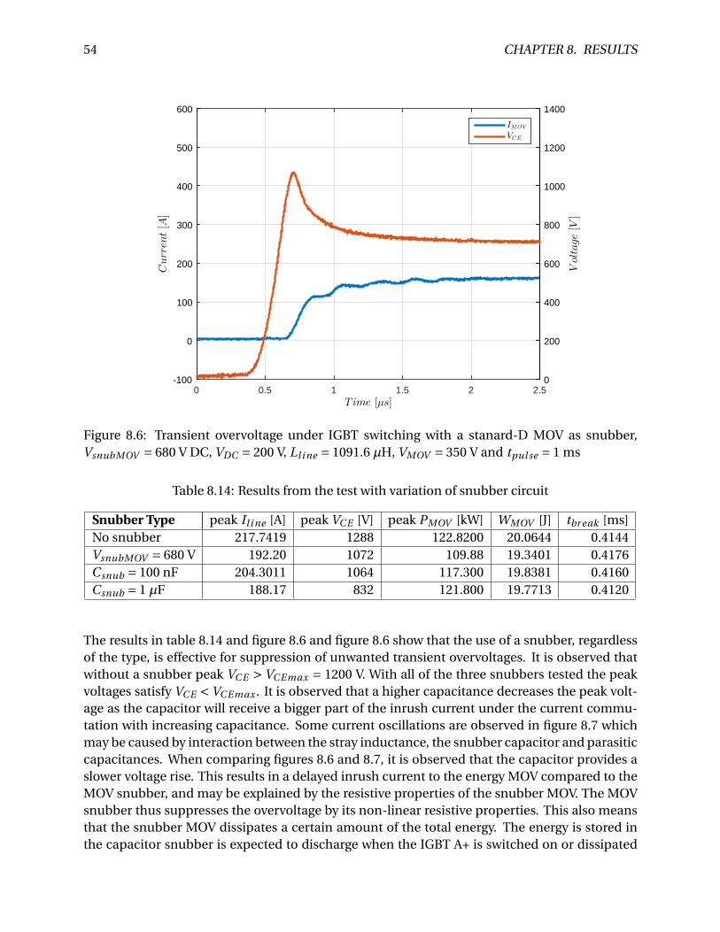
54 CHAPTER 8. RESULTS
Time [µs]0 0.5 1 1.5 2 2.5
Curren
t[A
]
-100
0
100
200
300
400
500
600
Voltage[V
]
0
200
400
600
800
1000
1200
1400
IMOV
VCE
Figure 8.6: Transient overvoltage under IGBT switching with a stanard-D MOV as snubber,VsnubMOV = 680 V DC, VDC = 200 V, Ll i ne = 1091.6 µH, VMOV = 350 V and tpul se = 1 ms
Table 8.14: Results from the test with variation of snubber circuit
Snubber Type peak Il i ne [A] peak VC E [V] peak PMOV [kW] WMOV [J] tbr eak [ms]No snubber 217.7419 1288 122.8200 20.0644 0.4144VsnubMOV = 680 V 192.20 1072 109.88 19.3401 0.4176Csnub = 100 nF 204.3011 1064 117.300 19.8381 0.4160Csnub = 1 µF 188.17 832 121.800 19.7713 0.4120
The results in table 8.14 and figure 8.6 and figure 8.6 show that the use of a snubber, regardlessof the type, is effective for suppression of unwanted transient overvoltages. It is observed thatwithout a snubber peak VC E > VC Emax = 1200 V. With all of the three snubbers tested the peakvoltages satisfy VC E < VC Emax . It is observed that a higher capacitance decreases the peak volt-age as the capacitor will receive a bigger part of the inrush current under the current commu-tation with increasing capacitance. Some current oscillations are observed in figure 8.7 whichmay be caused by interaction between the stray inductance, the snubber capacitor and parasiticcapacitances. When comparing figures 8.6 and 8.7, it is observed that the capacitor provides aslower voltage rise. This results in a delayed inrush current to the energy MOV compared to theMOV snubber, and may be explained by the resistive properties of the snubber MOV. The MOVsnubber thus suppresses the overvoltage by its non-linear resistive properties. This also meansthat the snubber MOV dissipates a certain amount of the total energy. The energy is stored inthe capacitor snubber is expected to discharge when the IGBT A+ is switched on or dissipated

8.3. CONTACTOR SWITCH TEST 55
Time [µs]0 1 2 3 4 5 6 7 8 9 10
Curren
t[A
]
-100
0
100
200
300
400
Voltage[V
]
0
200
400
600
800
1000
IMOV
VCE
Figure 8.7: Transient overvoltage under IGBT switching with a capacitor snubber Csnub = 100µF,VDC = 200 V, Ll i ne = 1091.6 µH, VMOV = 350 V and tpul se = 1 ms
in the energy MOV due to leakage currents. The energy stored in the capacitor is obtained byequation 5.2. The consequence of storing energy in a capacitor instead of dissipating energy inan MOV snubber is that the capacitor provides a slowly decreasing VC E until the IGBT A+ is setto on-state again or until the energy MOV has dissipated the stored energy.
8.3 Contactor Switch Test
The experiment is described in section 6.3. The result from switching Iswi tch = 1 A is shownin figure 8.8, and from switching Iswi tch = 0.15 A is shown in figure 8.9. When comparing thefigures, the time for the current to reach zero from its initial value differs significantly. An 1 Acurrent uses approximately around 2 ms to reach zero, while a 0.15 A current uses around 100µs.For both cases, high frequency voltage and current spikes occurs which indicates an arc is es-tablished. The voltage oscillations is approximately 500 V of magnitude which is higher than thethe source voltage of 300 V. For the 1 A current switching, seen in figure 8.8, the current is steadydecreasing before reaching zero and the extinction of the arc. At this point, the voltage againincreases to double the source voltage 600 V. In the figure 8.9 around 450 µs, similar overvoltageis observed simultaneously as the high frequency spikes. Apparently, also residual currents oc-curs. This is regarded as noise as the current clamp meter may react to the magnetic field of theelectromagnet inside the contactor switch.
In appendix B a switching including the voltages of the main and auxiliary contact is shown.
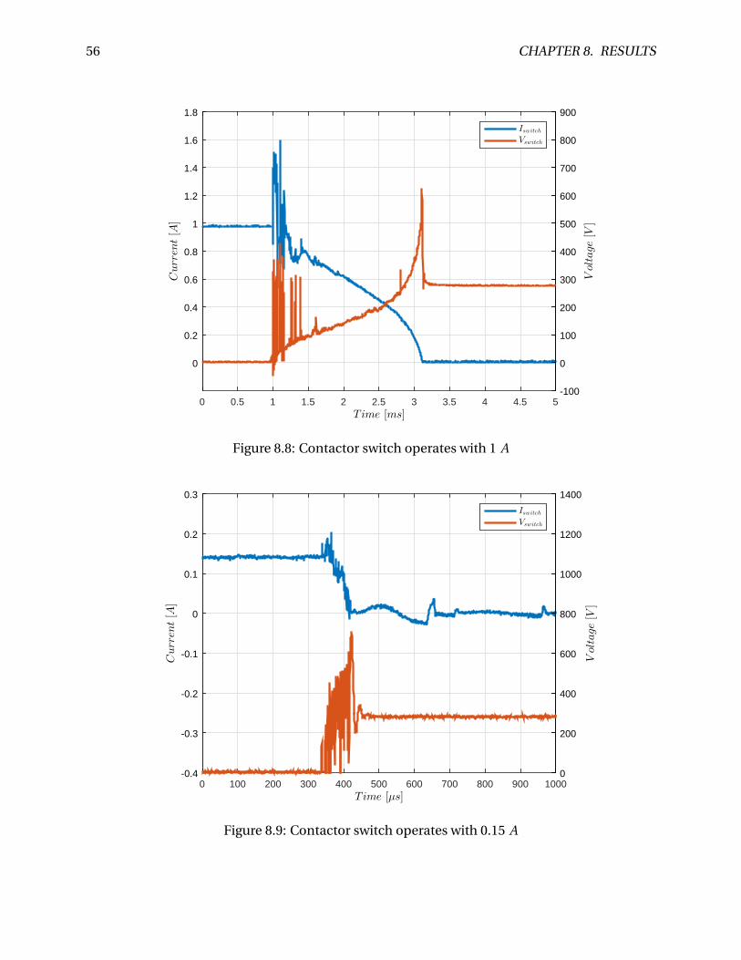
56 CHAPTER 8. RESULTS
Time [ms]0 0.5 1 1.5 2 2.5 3 3.5 4 4.5 5
Curren
t[A
]
0
0.2
0.4
0.6
0.8
1
1.2
1.4
1.6
1.8
Voltage[V
]
-100
0
100
200
300
400
500
600
700
800
900
Iswitch
Vswitch
Figure 8.8: Contactor switch operates with 1 A
Time [µs]0 100 200 300 400 500 600 700 800 900 1000
Curren
t[A
]
-0.4
-0.3
-0.2
-0.1
0
0.1
0.2
0.3
Voltage[V
]
0
200
400
600
800
1000
1200
1400
Iswitch
Vswitch
Figure 8.9: Contactor switch operates with 0.15 A
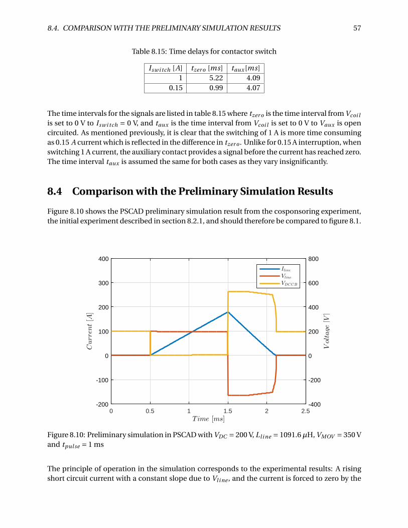
8.4. COMPARISON WITH THE PRELIMINARY SIMULATION RESULTS 57
Table 8.15: Time delays for contactor switch
Iswi tch [A] tzer o [ms] taux[ms]1 5.22 4.09
0.15 0.99 4.07
The time intervals for the signals are listed in table 8.15 where tzer o is the time interval from Vcoi l
is set to 0 V to Iswi tch = 0 V, and taux is the time interval from Vcoi l is set to 0 V to Vaux is opencircuited. As mentioned previously, it is clear that the switching of 1 A is more time consumingas 0.15 A current which is reflected in the difference in tzer o . Unlike for 0.15 A interruption, whenswitching 1 A current, the auxiliary contact provides a signal before the current has reached zero.The time interval taux is assumed the same for both cases as they vary insignificantly.
8.4 Comparison with the Preliminary Simulation Results
Figure 8.10 shows the PSCAD preliminary simulation result from the cosponsoring experiment,the initial experiment described in section 8.2.1, and should therefore be compared to figure 8.1.
Time [ms]0 0.5 1 1.5 2 2.5
Curren
t[A
]
-200
-100
0
100
200
300
400
Voltage[V
]
-400
-200
0
200
400
600
800
IlineVline
VDCCB
Figure 8.10: Preliminary simulation in PSCAD with VDC = 200 V, Ll i ne = 1091.6µH, VMOV = 350 Vand tpul se = 1 ms
The principle of operation in the simulation corresponds to the experimental results: A risingshort circuit current with a constant slope due to Vl i ne , and the current is forced to zero by the
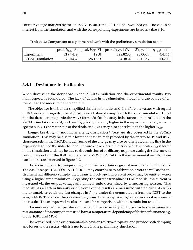
58 CHAPTER 8. RESULTS
counter voltage induced by the energy MOV after the IGBT A+ has switched off. The values ofinterest from the simulation and with the corresponding experiment are listed in table 8.16.
Table 8.16: Comparison of experimental work with the preliminary simulation results
peak Il i ne [A] peak VC E [V] peak PMOV [kW] WMOV [J] tbr eak [ms]Experiment 217.7419 1288 122.8200 20.0644 0.4144PSCAD simulation 179.0437 526.1323 94.3854 28.0125 0.6200
8.4.1 Deviations in the Results
When discussing the deviations in the PSCAD simulation and the experimental results, twomain aspects is considered: The lack of details in the simulation model and the source of er-rors due to the measurement technique.
The objective is to build a simplified simulation model and therefore the values with regardto DC breaker design discussed in section 8.1 should comply with the experimental work andnot the details in the particular wave form. So far, the stray inductance is not included in thePSCAD simulation model, and peak VC E is significantly higher in the experiment. A higher volt-age than in V-I characteristic of the diode and IGBT may also contribute to the higher VC E .
Longer break tbr eak and higher energy dissipation WMOV are also observed in the PSCADsimulation. This may be due to a lower counter voltage provided by the energy MOV and its VIcharacteristic in the PSCAD model. Some of the energy may also be dissipated in the line in theexperiments since the inductor and the wires have a certain resistance. The peak Il i ne is lowerin the simulation and may be due to the omission of oscillatory response during the line currentcommutation from the IGBT to the energy MOV in PSCAD. In the experimental results, theseoscillations are observed in figure 8.2.
The measurement techniques may implicate a certain degree of inaccuracy to the results.The oscilloscope, TEKTRONIX TDS 2014, may contribute to calibration errors as well as the in-strument has different sample rates. Transient voltage and current peaks may be omitted whenusing a higher time resolution. Regarding the current transducer LEM module, the current ismeasured via the output voltage and a linear ratio determined by a measuring resistor. Thismodule has a certain linearity error. Some of the results are measured with an current clampmeter unable to catch the fast changes in IMOV under the commutation from the IGBT to theenergy MOV. Therefore, the slow reacting transducer is replaced by a rogowski coil in some ofthe results. These improved results are used for comparison with the simulation results.
The environment temperature in the laboratory may vary and give rise to some minor er-rors as some of the components used have a temperature dependency of their performance e.g.diode, IGBT and MOV.
The wires used in the experiments also have an resistive property, and provide both dampingand losses to the results which is not found in the preliminary simulation.

8.5. PSCAD SIMULATION MODEL ADJUSTMENT 59
8.5 PSCAD Simulation Model Adjustment
8.5.1 Adjustments in PSCAD
The simulation model in PSCAD is adjusted to obtain a more realistic model. The objective is toobtain a similar operational behaviour of the DC breaker and values within a 10 % deviation tothe experimental work. The updated model has the following adjustments:
• Stray inductance of Lσ = 0.55 µH implemented.
• Apply a smaller solution time step tstep = 0.4µs to obtain the effect of the stray inductance.
• VI-characteristic of the energy MOV is adjusted according to the experimental work whichmeans adding more data points to the characteristic and apply a worst case 10 % toleranceband.
• VI-characteristic of the diodes and IGBTs is adjusted according to the experimental result.
• An auxiliary line resistor Rl i ne =100 mΩ is implemented for adjusting the energy dissipa-tion and break time tbr eak .
• An auxiliary capacitor Caux =0.5 nF is implemented in order to adjust the voltage spikes inPSCAD due to stray inductance and take the capacitive property of the energy MOV intoaccount.
The implementation of Lσ and the auxiliary capacitor is shown in figure 8.11.
Figure 8.11: The adjusted energy MOV branch in PSCAD with stray inductance and an auxiliarycapacitor
8.5.2 Results
The results from the adjusted simulation are presented in table 8.17 and in figure 8.12. It ob-served from the results that the obtained values, but peak line current Il i ne , in the adjustedPSCAD model deviate under 10%. As seen in figure 8.2, there are some oscillations during thecurrent commutation from the IGBT to the energy MOV which are not captured by the simula-tion. In the experiment, immediately before the commutation, Il i ne = 173 A seen in figure 8.2.

60 CHAPTER 8. RESULTS
Time [ms]0 0.2 0.4 0.6 0.8 1 1.2 1.4 1.6 1.8 2
Curren
t[A
]
0
100
200
300
400
500
600
Voltage[V
]
0
200
400
600
800
1000
1200
IlineVCE
Figure 8.12: Simulation of the adjusted PSCAD model with VDC = 200 V, Ll i ne = 1091.6 µH,Rl i ne = 100 mΩ, VMOV = 350 V, tpul se = 1 ms and Lσ = 0.55µH
I.e. is the peak line current due to the current slope provided by Ll i ne . The additional contri-bution form the oscillation is ∆Il i ne = 44.5 A. The effect of the stray inductance is visible as avoltage spike in figure 8.12. Obtaining a more realistic damped oscillatory wave form requires
Table 8.17: Comparison of experimental work with the adjusted simulation results
peak Il i ne [A] peak VC E [V] peak PMOV [kW] WMOV [J] tbr eak [ms]Experiment 217.7419 1288 122.8200 20.0644 0.4144PSCAD simulation 170.98 1176.32 120.79 21.957 0.3900
a smaller solution tstep and a more detailed model. An attempt of obtaining the oscillatory re-sponses in PSCAD for a DC breaker has been made in [50]. Some oscillations are observed aftershort circuit clearance in figure 8.12. These are not found the corresponding experiment, andthis may due to the interaction between Ll i ne the auxiliary capacitor and Rl i ne .
The PSCAD simulations of the test model is assumed adequate for further design processas the operation principles are obtained and the values of importance discussed in section 8.1deviates under a 10% limit.

Chapter 9
Development of the DC Breaker Design
This chapter aims as selecting the components for the design of the DC breaker in the NTNU/SINTEFlab and determine the corresponding ratings.
9.1 Corner Cases
The DC breaker for the NTNU/SINTEF laboratory may have to interrupt currents under severaldifferent circumstances. Therefore the following corner cases are considered for the interpreta-tion of the results provided in chapter 8, facilitating the selection of components and determi-nation of parameters ratings for the final DC breaker design.
1. Active region current interruption. The IGBT is operating in its active region under currentinterruption.
2. Instant high short circuit current interruption. Short circuits near the capacitor bank/DClink with little or zero inductance.
3. Current interruption with maximum magnetic energy. Short circuits with high induc-tance.
4. Auto-reclosing of the DC breaker to a permanent fault. The DC breaker is demanded tointerrupt 2 short circuits within a small time interval.
5. Repetitive load switching. The DC breaker is used for sectioning loads in the DC grid.
6. DC grid black start. DC breaker used for charging DC capacitor bank on the opposite side.
Case 1 represents a corner case in which the IGBT operates in the active region described in sec-tion 4.1.2. This operating state may lead to additional power loss and subsequently undesirableheating of the IGBT. The gate driver used in the test model has implemented a protection abil-ity which trips under excessive voltage drops over the IGBT. This case is not treated in furtherdevelopment of the DC breaker, since protection is already implemented in the gate driver
Case 2 represents a corner case where the current will rise rapidly due to low inductance,typically for short circuits near the converter. A certain response time between the detectionof the short circuit and the trip of the DC breaker can be expected from the protection system.
61

62 CHAPTER 9. DEVELOPMENT OF THE DC BREAKER DESIGN
The rapid rise in current continues during the response time interval, and there will be a certainrisk of the current breaking capability of the DC breaker being exceeded. Accordingly the re-sponse time, the current breaking capability and minimum short circuit inductance should beconsidered in the DC breaker design.
In case 3 the energy in the system, described in section 3.3, may exceed the energy MOVsrated maximum energy dissipation WMOV max due to the magnitude of line inductance Ll i ne .Therefore WMOV max in relation to the maximum line inductance should be considered. Case 4stresses the ability of the DC breaker of interrupting at least two repeating short circuits promptly.The case is actual if the protection system is designed with an ability for auto-reclosing lines.
Case 5 refers to a situation in which the DC breaker switches load currents in order to sectionvarious parts of the DC grid. Therefore, the DC breaker ability to interrupt currents around 1 purepetitively should be considered.
In case 6, the DC breaker is used for charging the capacitor bank of the VSC on the oppositeside of the DC line. The case may be relevant in a black start situation where the capacitorbank inrush current during the charging may exceed the current breaking ability. Some chargingseries resistance in the DC line may limit this effect.
This chapter consider cases 2 and 3 in more detail as they concern the main function of acircuit break; to interrupt fault currents. A brief discussion is also given on the repetitive currentinterruption related to case 4 and 5.
9.2 Discussion of the Results for the Final DC Breaker Design
This section discusses the results in the previous chapter in relation to the design of a DC breakerand the limitations on the components.
9.2.1 The IGBT in Relation with the energy MOV
The energy MOV protects the IGBT from a harmful transient interruption voltage (TIV) duringthe current interruption as the line current is commentated into the energy MOV and providinga counter voltage. Assuming the DC breaker had consisted of IGBT modules only, the TIV maycontribute to IGBT failure as the TIV would be very high as described in section 3.1.2. The exper-imental results indicate that a counter voltage must be higher than the source voltage with thecombination of an inductance. This accounts for all current magnitudes intended to be forcedto zero. Both sufficient line inductance and the counter voltage must therefore be ensured whendetermining an energy MOV for the DC breaker. Section 8.2.5 describes how an increase in thevoltage rating of the energy MOV reduces the break time tbr eak and the energy dissipated pershort circuit clearance. A high voltage rating is beneficial for a rapid short circuit clearance.However the voltage rating of the energy MOV should not be determined as high as possible inthe DC breaker design. The VC E also rises correspondingly with rising VMOV , and VC Emax maybe exceeded. The line current Il i ne may also limit the rated MOV voltage. A higher interruptedcurrent provides a higher energy MOV voltage and possible VC E > VC Emax . When the energyMOV operates in the protecting region, referred to in 4.2.2, the results shows only a marginalincrease in the MOV voltage. VC Emax may however be exceeded if the DC breaker interruptscurrents corresponding to a situation in which the energy MOV operates in the linear region.

9.2. DISCUSSION OF THE RESULTS FOR THE FINAL DC BREAKER DESIGN 63
9.2.2 The Snubber Circuit
In order to examine the effect of a snubber type, the results in section 8.2.6 indicated that both asnubber MOV and a capacitor were effective suppressors of undesired voltage transients causedby stray inductance. The snubber MOV has the advantage of dissipating energy, as opposedto the capacitor which only stores energy. The applications of a DC breaker is not intendedto switch in similar high frequencies as IGBTs in a VSC. The energy discharge is also assumedless critical. Due to leakage currents, the energy MOV in parallel may also dissipate some ofthe stored capacitor energy. The snubber may accordingly have a high capacitance and providebetter protection capability which also was indicated in the results in table 8.14. However, itwas also seen that a higher capacitance may increase the total time of short circuit clearance asthe voltage rise is slower. The capacitor represents a more conventional solution than a snubberMOV for IGBT protection, and is thus the recommended solution for the final DC breaker design.
9.2.3 Thermal Considerations of the Energy MOV
Two main aspects observed in the results regarding the thermal considerations of the energyMOV: The energy dissipated per current interruption and the leakage currents.
Current Interruption
DC breaker current interruption is assumed related to both the single impulse handling capa-bility and the thermal energy handling capability described in section 4.2.4. During currentinterruption a high incoming current to the MOV is observed initially and thereafter a decreas-ing continuous current which time duration may vary. As seen in figure 8.4, the temperaturerise per current interruption is assumed insignificant since the MOV is not exceeding its criticaltemperature TMOV = 85° C with repeating short circuit interruptions for certain time. The in-ductance intended to be used in DC grid in the NTNU/SINTEF lab may however be significantlyhigher than the inductor used in the experiments. The magnitude of inductance in relation tothe number of energy MOVs related to maximum current should therefore be analysed. Whenconsidering repeating stitchings within small time intervals, it should also be ensured that thetotal energy dissipated is less than the rated maximum energy dissipation WMOV max and theaverage power within PMOV max . In section 8.2.5 the cooling time constant was calculated fromexperimental data to approximately 7 min. This indicates that the energy MOV needs a cer-tain time to cool before a new high-energy interruption may occur.This is in order to avoid therisk overheat. The requirement could affect the ability of the DC breaker to conduct repetitivecurrent interruptions.
Leakage Currents
Under normal operation of a DC grid the leakage current of the energy MOV is determined bythe voltage drop over the parallel current conducting IGBTs and diodes. The voltage drop shouldbe of such range that the leakage current is too small to generate power losses which could causeheating of the energy MOV to the critical temperature. For the DC breaker for the NTNU/SINTEFlaboratory, the non-continuous operation of the DC grid will be prevent this effect. This is con-sidered to be of greater relevance for DC breakers in an operating HVDC grid.

64 CHAPTER 9. DEVELOPMENT OF THE DC BREAKER DESIGN
After the short circuit current has been forced to zero, residual currents may also provideheating. The energy MOV leakage current and high frequency current oscillations (occurringdue to a low line inductance Ll i ne seen in figure 8.3) both contribute to the residual currents.A contactor switch should accordingly operate, in order to provide isolation as soon as possi-ble after the line current, excluding residual current, is forced to zero. The voltage over the DCbreaker, and thereby the energy MOV, will approximately be the same as the voltage source seenin figure 8.1. At this point more leakage current will flow than under normal operating condi-tions described in the previous paragraphs. If the rated operating voltage of the energy MOV isless the than voltage of the source, excessive leakage current may flow and lead to heating andeventually failure if PMOV max is exceeded. The negative temperature coefficient may also implya self-amplifying effect of the heating which stresses a recommendation for the contactor switchto operate as fast as possible.
The energy MOV may absorb some of the heat generated in the semiconductors. As such,the location of the energy MOV should ideally minimise the heat transferred into it from theIGBT modules.
9.2.4 Thermal Considerations of the IGBT/Diode modules
So far, thermal considerations of the IGBT and the diode have not been undertaken. The testmodel provides a limited ability to examine the thermal features of the semiconductors in aDC breaker. The thermal design elements of the DC breaker will accordingly be consideredalongside the simulation and testing of the final design, before the DC breaker is assembled.The IGBT modules typically have a maximum junction temperature limitation refeered as T j max
under steady state normal operation. The power loss transferred into heat may thus limit themaximum rated steady state current that could run through the DC breaker
Main Points from the Discussion
The main aspects discussed in this section can be summarised as:
• The counter voltage of the energy MOV must be higher than the source voltage.
• The counter voltage of the energy MOV must not exceed the rated collector-emitter volt-age VC Emax .
• The magnitude of the interruption current should be in the protecting region of the energyMOV.
• The IGBT should have a snubber circuit protecting for transient overvoltages due to strayinductances.
• The rated operating voltage of the energy MOV VMOV should not exceed the source volt-age.
• The contactor switch should isolate immediately after the line current is forced to zero.
• The contactor switch must interrupt the residual currents and withstand residual voltagesafter operating.

9.3. DC BREAKER RATINGS 65
9.3 DC Breaker Ratings
Based upon what has been discussed so far in this chapter, the necessary ratings of the DCbreaker include:
Rated current The DC breaker current under normal operation. I.e. the rated nominal currentof the system.
Current breaking capability The maximum current the DC breaker is capable to interrupt.
Overload current The maximum continuous steady state DC breaker current.
Rated voltage The voltage of the system the DC breaker is designed for.
Maximum withstand capability The maximum voltage DC breaker can withstand after currentinterruption.
Voltage margin The minimum tolerated margin between the VC E and VC Emax and under cur-rent interruption.
Maximum operating temperature The maximum operating temperature of the semiconduc-tor devices in the DC breaker.
Maximum and minimum line inductance
Repetitive current interruption capability
9.4 Selection of Components
The selection of components will first be established in a way that ensures the capability of theDC breaker to interrupt currents and minimises the risk of component failure. This is initiallydone by manual calculations followed by an analysis in section 9.5 including limitations andratings of the design, partially based on PSCAD simulations
9.4.1 Selction of IGBT Modules
The test model seen in figure 6.5 and 6.4 consists of only one DC breaker cell. More cells in seriesmay represent an alternative if a higher counter voltage is needed in order to reduce the breaktime and limit the energy dissipation of the energy MOV. The drawback of having a number of Mbreaker cells in series is that the conduction losses will be as M times as higher. This would alsorequire more space, be more costly and require more with regard to the thermal considerations.An alternative is to use high voltage IGBTs (HVIGBT). More breaking cells or HVIGBTs generatemore conduction losses and hence increase the need for a more complicated auxiliary coolingsystem. Active cooling for the DC breaker design, especially using other cooling media than air,may complicate the design and the control system of the breaker. Moreover the HVIGBTs areassumed to have a higher cost. Table 9.1 shows an example of a the losses of different configu-rations with 1 pu (100 A) of the 60 kVA lab VSC. The resistive loss approach in section 4.1.2 and

66 CHAPTER 9. DEVELOPMENT OF THE DC BREAKER DESIGN
Table 9.1: Comparison of IGBT modules for the DC breaker design [53, 54]
IGBT type Cells VC Emax [V] DC Breaker Ploss [W]Mitsubishi HVIGBT 1 3300 430.0Mitsubishi HVIGBT 2 3300 860.0Infineon IGBT 1 1700 211.93Infineon IGBT 2 1700 423.86
the data sheets is used to estimate the loss the total DC breaker loss Ploss . Appendix C presentsthe details regarding the calculations. The conduction losses of both HVIGBT and of a 2 cell In-fineon 1700 V DC breakers are assumed too high for the DC breaker intended for the DC grid inNTNU/SINTEF lab. A one-cell DC breaker design with Infineon 1700 V IGBT is therefore recom-mended. Whilst this would extend the breaking time, it would also minimise the space required,the conduction losses, the cost and the need for a complicated cooling system. For the recom-mended module, the rated maximum collector current is ICr m = 1200 A=12 pu for a 1 ms currentpulse.
9.4.2 Selection of Heat Sink
The thermal resistance is related to the power loss of semiconductors and is described in sec-tion 5.2.1. An electro thermal circuit may be useful in order to estimate the temperatures of thejunction of the semiconductor and facilitate the selection of a heat sink and a cooling system.For the DC breaker a simple solution with an air-cooled heat sink is recommended. For the rec-ommended IGBT module, the rated maximum junction temperature is T j max = 150 °C. Usingequation 5.8, assuming a Ta = 25 °C and 1 pu continuous current, Rθ j a = 0.60 K/W along theheat conduction path is calculated. The data sheet provides the equivalent thermal resistanceof 0.091 K/W for the diode and 0.056 K/W the IGBT. A standard extruded aluminium heat sinktype SK 425 with Rθheat si nk = 0.2 K/W is the recommended heat sink [55]. This heat sink has oneof the lowest Rθheat si nk in the catalogue and ensures that junction temperature T j max = 150 °Cwill not be exceeded with 1 pu continuous current.
9.4.3 Selction of Energy MOV
The energy MOV should have a rated operating voltage VMOV higher than the source voltage.During current interruption, the counter voltage provided by the energy MOV must not exceedVC Emax . The corresponding current to VC Emax may accordingly limit the current breaking ca-pability. A voltage margin Vmar g i n may be included in order to ensure that VC Emax is neverexceeded. The 10 % tolerance of the VI-characteristic must also be taken into account in thesecalculations. The energy MOV recommended is a high energy MOV type B60K460 with the fol-lowing ratings: VMOV = 615 V, VV = 750 V and clamping voltage Vc (Ic ) = 1250 V and Ic = 500.Assuming a capacitor snubber mitigates the effect of the stray inductance and using the datasheet, the selected varistor provides a voltage margin Vmar g i n = 450 V when the DC breaker in-terrupts a 5 p.u or 500 A current. Given Vmar g i n = 0 V by using equation 4.5, the maximumcurrent capability is determined to approximately 5925 A. This current magnitude exceeds the

9.5. PSCAD SIMULATIONS AND DETERMINATION OF RATINGS 67
repetitive peak current ICr m . The calculation indicates that ICr m is the limiting factor for therated current breaking capability. The calculation is attached in appendix C.
As mentioned, the rated MOV voltage VMOV should be lower than the rated voltage of theconverter VDC . This is not the case with the selected energy MOV, meaning that after the cur-rent interruption, the MOV will conduct a certain leakage current i.e IMOV (750 V ) =1 mA. Thecontractor switch must interrupt this current and ensure PMOV < PMOV max . At rated convertervoltage 700 V the expected MOV power PMOV =0.71 W which is lower than rated PMOV max . Thiscalculation assumes that the energy MOV maintains a normal temperature. If the temperatureof the energy MOV exceeds Tcr i t i cal = 85 °C, more leakage current is expected. The contactorswitch should therefore operated as fast as possible.
Using two energy MOVs in parallel with the IGBT modules of the type mentioned is the rec-ommended solution for handling higher energy dissipation due to the line inductance Ll i ne .An analysis of maximum current breaking capability in relation to the line inductance will becarried out in a following section.
9.4.4 Selection of Contactor Switch
As stated in previous section, the expected leakage current is around 1 mA, and as seen in sec-tion 8.2.2, the current oscillation may be insignificant due to damping before the switch oper-ates. A contactor switch also has a certain time-delay investigated in section 8.3 The selectedcontactor switch is the same as previously tested (section 8.3); KILOVAC EV200. The contactoris designed for DC applications, and the results showed that it was able to isolate and break theexpected residual current despite highly a inductive load. The rated voltage of the contactor is900 V, which is higher than the rated voltage of the DC grid. Accordingly, the switch should beable to both operate and isolate. According to the data-sheet, the recommended contactor alsotolerates a current of 2000 A for 12 ms not risking contact welding and failure [47].
Selected Components
Based on the discussion and investigations undertaken, the recommendations for the design ofthe DC breaker in terms of components are summarised as follows:
IGBT module VC E =1700 V FZ600R17KE3 IGBT/Didoe-module [54]
Heat sink SK425 extruded aluminium [55]
Energy MOV VMOV = 615 V DC B60K460 EPCOS HighE series block varistor [56]
Contacor switch KILOVAC EV200 [47]
9.5 PSCAD Simulations and Determination of Ratings
PSCAD simulation of the DC breaker will be used to calculate the ratings of the DC breakerlisted in section 9.3. The details regarding the outline of the PSCAD simulation model is de-scribed in chapter 7. The PSCAD model is also adjusted using conservative component param-eters in the simulations in order to ensure the results obtained. In the adjusted simulations,
68 CHAPTER 9. DEVELOPMENT OF THE DC BREAKER DESIGN
described in section 8.5.1, the VI-characteristic is observed more conservative than using theVI-characteristic of T j = 25 °C. The IGBT and diode VI-characteristic for operation at T j = 125°C is implemented. The MOV VI-characteristic is implemented with a 10% tolerance band fromthe data sheet (I.e. maximum voltage is assumed for a given current). The temperature of the en-ergy MOV is assumed TMOV < Tcr i t i cal = 85°C such that no de-rating applies. A source voltageVDC = 700 V or 1 pu, is assumed for all simulations, and stray inductance is omitted as a ca-pacitor snubber is assumed with Csnub = 0.1 µF. The removal of stray inductance also providesefficient simulation time since the time tstep may be increased accordingly.
9.5.1 Principle of Operation
Table 9.2: Parameters used in PSCAD for validation of the selected components
Parameter ValuesLl i ne 10 mHtr esponse 0.1 msPre fault Il i ne 1 puItr i p 3 puRl i ne 1 mΩCsnub 0.1 µF
The following case listed in table 9.2 is simulated in PSCAD order to validate the selectionof components. Plots of the voltage of the switching IGBT is shown in appendix D. The valuesobtained is listed in table 9.3. The currents and voltages obtained form the simulation is shownin figure 9.1 and the temperature rise in the same time interval is shown i figure 9.2. With thissimulation, the consequence of having only one breaker cell is seen as the break time tbr eak is6.4 ms. The counter voltage is lower, and therefore also longer tbr eak provided and more energyis dissipated in the energy MOV. Regarding the the temperature rise, it is observed that the shortcircuit generated a temperature rise in the IGBT and the anti-parallel diode. The diode is risingfaster and higher as the time constant is the lowest for the the corresponding heat conductionpath. The heat sink temperature is not effected as the time constant τheat si nk is higher.
Table 9.3: Values obtained in PSCAD with the selected components for the DC breaker
peakT j di ode peakT j IGBT peak Il i ne [A] peak VC E [V] peak PMOV [kW] WMOV [J] tbr eak [ms]76.57 70.67 307.2 1210.97 371.13 1136.4 6.4
9.5.2 Current Breaking Capability
Consideration of Line Inductance
The repetitive peak current ICr m which has been discussed as a limitation for the current break-ing capability – represents the starting point for the determination of the maximum currentcapability. The next step is to evaluate the limitation of the line inductance Ll i ne corresponding
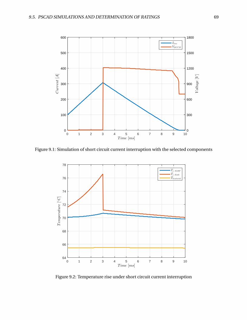
9.5. PSCAD SIMULATIONS AND DETERMINATION OF RATINGS 69
Time [ms]0 1 2 3 4 5 6 7 8 9 10
Curren
t[A
]
0
100
200
300
400
500
600
Voltage[V
]
0
300
600
900
1200
1500
1800
IlineVDCCB
Figure 9.1: Simulation of short circuit current interruption with the selected components
Time [ms]0 1 2 3 4 5 6 7 8 9 10
Temperature[C]
64
66
68
70
72
74
76
78
Tj IGBT
Tj diode
Theatsink
Figure 9.2: Temperature rise under short circuit current interruption

70 CHAPTER 9. DEVELOPMENT OF THE DC BREAKER DESIGN
to the energy MOV WMOV max in terms of peak Il i ne . Equation 3.9 expresses theoretically thetotal energy the MOV needs to dissipate if no resistive elements in the DC line is assumed. Forworst case consideration, the resistive element is also neglected in the following simulations.The selected energy MOV has rated WMOV max = 1650 J. Since the MOV may have some leakagecurrent prior to DC breaker trips, such that WMOV max = 1600 J is assumed in further simula-tions. Two parallel energy MOVs results in WMOV max = 3200 J. The maximum current breakingcapability Imax with 2 parallel energy MOVs as a function of the line inductance Ll i ne obtainedfrom PSCAD is shown in figure 9.3. Here, ICr m is taken into account, while the voltage marginis analysed later point on. The figure also presents the detection level of the overcurrent protec-tion Itr i p , where the response time is assumed tr esponse = 0.1 ms. Corresponding figures withother tr esponse are attached in appendix E.
Line inductance Lline [mH]10-2 10-1 100 101 102
Current[pu]
0
2
4
6
8
10
12
14
Imax
Itrip
Figure 9.3: The current breaking capability Imax as a function line inductance Ll i ne , Imax is thepeak current interrupted and Itr i p is the maximum detection level of the protection system,tr esponse = 0.1 ms
It is observed that there are 2 areas of Imax . For Ll i ne > 2 mH, the MOVs ability to dissipateenergy Wmax determines Imax . And for Ll i ne <2 mH, ICr m =12 pu determines Imax . If moreMOVs were placed in parallel, the area in which Imax = ICr m is expected to shift to the right inthe figure, as the DC breaker will be able to dissipate more of the energy. For Ll i ne > 2 mH , Imax
decreases with an increasing Ll i ne . As seen in the experiments with the test model, the voltagedrop over the energy MOV or the DC breaker only changes marginally with respect to the cur-rent when operating in the protective region. By considering equation 3.9, Il i ne decreases withthe square root of the current Imax as the VC B only changes marginally. In the left area, whereLl i ne < 2 mH, also a significant effect of tr esponse is observed. The inductance determines the

9.5. PSCAD SIMULATIONS AND DETERMINATION OF RATINGS 71
slope of the short circuit current seen in 3.3. If the Ll i ne is relatively small, and the the responsetime has a certain magnitude, the detection level and the peak current will differ significantly.In figure 9.3 at Ll i ne < 0.05 mH, the current will rise so fast such that ICr m is exceeded beforethe short circuit current is interrupted. This also illustrates the importance of determining min-imum line inductance. Assuming tr esponse =0.1 ms, the recommended minimum line induc-tance is 0.7 mH. Here the detection level must be set to 2 pu and the DC breaker will interrupt12 pu.
Consideration of Energy MOV Voltage
Voltage margin Vmargin [V ]250 300 350 400 450 500
Current[pu]
0
2
4
6
8
10
12
Imax
Figure 9.4: The current breaking capability Imax as a function of the desired voltage marginVmar g i n
Figure 9.4 shows the voltage margin Vmar g i n obtained from simulations. For the selectedMOV and IGBT, 250 < Vmar g i n(ICr m) < 300. The voltage margin only determines the currentbreaking capability if Vmar g i n >300 V. A voltage margin Vmar g i n = 250 V should be sufficient asthe capacitor snubber worked effectively in the experiments described in section 8.2.6. As statedin section 9.4, interruption of a 5 pu current provides Vmar g i n = 450 V. According to figure 9.4,the Vmar g i n ≈ 425 V which is explained by the MOV VI-characteristic implemented in PSCADmay lack details. However, since it is already stated that the ICr m will be the limiting factor ifVmar g i n = 250 V, adjustments in PSCAD are not considered necessary. Since two dependenciesare observed in figure 9.3 and Ll i ne may be varied in the DC grid, two types of rated maximumcurrent capability are determined according to figure 9.3. One value for high energy currentinterruption and another for lower energies/lower Ll i ne is determined. The high energy type:

72 CHAPTER 9. DEVELOPMENT OF THE DC BREAKER DESIGN
Ll i ne = 20 mH and Imax = 3.5 pu. Low energy type: Ll i ne = 1 mH and Imax = 12 pu.
9.5.3 Maximum Continuous Current
Line current Iline [A]80 100 120 140 160 180 200 220
Tem
perature[C]
50
75
100
125
150
175
200
Tj IGBT
Tj diode
Theatsink
Figure 9.5: DC breaker temperatures as a function of the continuous line current Il i ne
The maximum continuous current is found by simulating a steady state case of the DC gridwith continuous line current Il i ne and finding the corresponding Il i ne in which the T j = T j max =150 °C. The electro thermal circuit described in section 7.5 is used. In figure 9.5 the temperatureof the heat sink Theat si nk , diode junction T j di ode and the IGBT junction T j IGBT is shown. T j di ode
exceeds the maximum contentious temperature at Il i ne = 210 A. The recommended maximumcontinuous current is thus 2 pu with a safety margin of 10 A. However, a fan may decrease thethermal resistivity of the heat-sink and also contribute to avoid excessive heat transfer to theenergy MOV. The fan may be started by a temperature relay placed on the heat sink surface.This will start air-cooling when needed if the Theat si nk exceeds a certain level.
9.5.4 Maximum Voltage Withstand Capability
As seen in the results of from contactor test experiment, under and after current interruptionresidual transient voltages occurs. The contactor switch must be able to withstand this in orderto prevent the arc from re-ignition. The rated withstand voltage of the selected contactor switchis Vw = 2200 V.

9.5. PSCAD SIMULATIONS AND DETERMINATION OF RATINGS 73
9.5.5 Repetitive Current Interruption Capability
As discussed in section 9.1 the DC breaker may be used to interrupt currents more than oncewithin a given time frame. It is suggested that PMOV max and WMOV max for the energy MOV maybe used to determine the repetitive current interruption capability. It is assumed that the DCbreaker can interrupt currents as long as the average power of the energy MOV is kept withinPMOV max , and the temperature is below the critical temperature TMOV = 85 °C. For switchingload currents, 1.5 pu current interruption with Ll i ne = 10 mH is assumed. The values may beadjusted later. For the selected energy MOVs in the suggested parallel configuration, the ratingsare: PMOV max = 3.2 W and WMOV max = 3200 J. The residual current contribution before thecontactor switch opens should also be considered as it may contribute to the PMOV . Simulationin PSCAD provides PMOV = 1.5 W. The delay time of the of the contactor switch is measured to 4ms in which the total energy dissipation is assumed insignificant. Simulation of the mentionedload current switching provides WMOV = 282 J per switching. In theory, this means that the timeduration between the switching should be t = 282 J/3.2 W = 88.1 s, almost 1.5 minute betweeneach switching. Therefore the suggested solution to obtain the repetitive current interruptioncapability is to measure the temperature of the energy MOV under repetitive load currents andshort circuits while ensuring TMOV < Tcr i t i cal = 85 °C . Most likely, the surface temperature ofthe MOV is measured and must be taken into consideration.
Given that the main function of a DC breaker is to interrupt fault current, and taking intoaccount the ratings related to the short circuit interruption have been obtained, the repetitivecurrent interruption is of less importance.
9.5.6 Summary of DC Breaker Ratings
The following list summarizes the main results form this section.
Rated current 100 A
Current breaking capability Low inductive: 1200 A High inductive: 350 A
Overload current 200 A, expected to decrease with active cooling.
Rated voltage 700 V
Maximum Withstand Capability 2200 V
IGBT Voltage Magin 250 V
Maximum operating temperature 150°C
Maximum and Minimum Line Inductance Maximum:20 mH and minimum: 0.7 mH
Repetitive Current Interruption Capability Determined when DC breaker is tested.

74 CHAPTER 9. DEVELOPMENT OF THE DC BREAKER DESIGN
Chapter 10
Implementation of the DC Breaker
This chapter describes the implementation of the DC breaker for the NTNU/SINTEF lab.
10.1 Configuration of the DC Breaker
Two similar DC breakers is implemented, one for the positive pole and one for the negativepole of the 60 kVA laboratory converter. The components used are the selected components inprevious chapter. The final DC breaker configuration consist of the following:
Solid state DC breaker Two IGBT modules in anti-series, capacitor snubbers Csnub and a par-allel MOV.
Isolator Switch Contactor switch referred to as IS for physical isolation
Bypass Switch Contactor switch referred to as BS to bypass the DC breaker when not in use.
Charging circuit Contacor switch referred to as CS and charging resistor Rc .
The circuit diagram is shown in figure 10.1. The DC breakers has a bi-directional current in-terruption possibility as the IGBT modules are placed in anti-seires. The configuration hasincluded functionality for charging the adjacent DC capacitor bank, and the parallel chargingresistor Rc = 22 kΩ will reduce the inrush current. In parallel with the solid state breaker, a by-pass path is implemented in order to operate the DC grid in the NTNU/SINTEF lab without theDC breaker and also for emulating a hybrid DC breaker topology at a later point. The snubbercircuit is added to each IGBT with Csnub = 0.1 µF. In appendix F, a detailed circuit diagram isillustrated with the control system. The control system is based on simple 24 V DC electro me-chanical relays. This is expected to be developed further as the DC breaker is tested. E.g. A fieldprogrammable gate array (FPGA) is attached to the control system, but not currently in use.
75
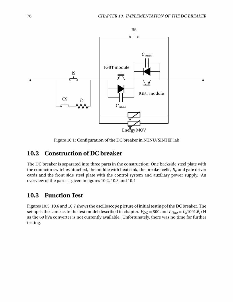
76 CHAPTER 10. IMPLEMENTATION OF THE DC BREAKER
CS Rc
IS
U
U
Energy MOV
Csnub
Csnub
BS
IGBT module
IGBT module
Figure 10.1: Configuration of the DC breaker in NTNU/SINTEF lab
10.2 Construction of DC breaker
The DC breaker is separated into three parts in the construction: One backside steel plate withthe contactor switches attached, the middle with heat sink, the breaker cells, Rc and gate drivercards and the front side steel plate with the control system and auxiliary power supply. Anoverview of the parts is given in figures 10.2, 10.3 and 10.4
10.3 Function Test
Figures 10.5, 10.6 and 10.7 shows the oscilloscope picture of initial testing of the DC breaker. Theset up is the same as in the test model described in chapter. VDC = 300 and Ll i ne = L31091.6µ Has the 60 kVa converter is not currently available. Unfortunately, there was no time for furthertesting.
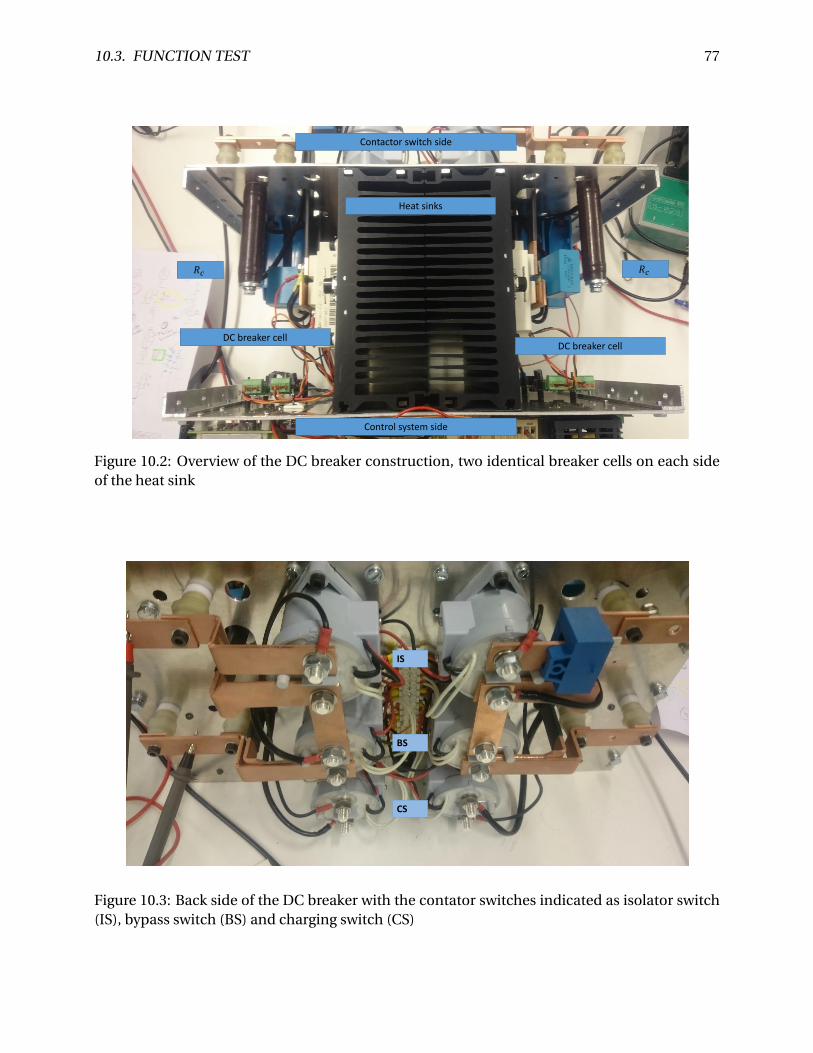
10.3. FUNCTION TEST 77
Contactor switch side
Control system side
DC breaker cellDC breaker cell
Heat sinks
𝑅𝑐 𝑅𝑐
Figure 10.2: Overview of the DC breaker construction, two identical breaker cells on each sideof the heat sink
IS
BS
CS
Figure 10.3: Back side of the DC breaker with the contator switches indicated as isolator switch(IS), bypass switch (BS) and charging switch (CS)

78 CHAPTER 10. IMPLEMENTATION OF THE DC BREAKER
MOV
IGBT module𝑪𝒔𝒏𝒖𝒃
Gate driver
𝑹𝑪
Figure 10.4: One side of the middle part of the DC breaker

10.3. FUNCTION TEST 79
Figure 10.5: Current interruption in final breaker design, CH1 depicts the IGBT voltage, CH2the breaker cell voltage and CH3 depicts the current measured as voltage from the LEM-module(ratio: 1/20)
Figure 10.6: Current interruption in final breaker design, CH1 depicts the IGBT voltage, CH2the breaker cell voltage and CH3 depicts the current measured as voltage from the LEM-module(ratio: 1/20)

80 CHAPTER 10. IMPLEMENTATION OF THE DC BREAKER
Figure 10.7: Transient overvoltage under current interruption in final breaker design, CH1 de-picts the IGBT voltage, CH2 the breaker cell voltage and CH3 depicts the current measured asvoltage from the LEM-module (ratio:1/20)

Chapter 11
Guidelines for DC Breaker Design
The purpose of this chapter is to provide design guidelines for HVDC breakers. The basis is thedevelopment of the solid state DC breaker in previous chapters and put the experiences in thecontext of a HVDC transmission system.
11.1 Circuit Breakers for HVDC Applications
The DC breaker for the NTNU/SINTEF lab is a solid state DC breaker. In the experimental workand simulations, one of the main advantages of the topology is observed. The type of DC breakerhas the capability to interrupt currents fast e.g. the results provided a break time tbr eak under1 ms in in chapter 8. The disadvantage of the topology is the on-state conduction losses as thesemiconductors must be placed in the series with DC line. As mentioned, the counter voltagemust be higher than the system voltage in order to force the current to zero. The semiconduc-tor devices have a recommended voltage drop limit,VC Emax for the IGBT, and must be able totolerate a voltage magnitude equal or bigger than the counter voltage. For a higher system volt-age of the DC grid, the higher amount of semiconductors is needed in series with the line andthus provide a significant amount of losses. Ratings from the CIGRE DC grid test system is usedto illustrate the number of semiconductors needed [57]. The examples assumes a bi-directionalcurrent interruption application. If a solid state DC breaker shall provide a counter voltage of 1.3pu of a 400 kV overhead line (OHL) in the DC grid, the requirement is at least 158 breaker cellsconsisting of two 3.3 kV Mitsubishi IGBT modules each in series with the DC line. As seen insection 9.4 for a 100 A current, the loss is Ploss = 430 W per breaker cell. For the actual IGBT themaximum rated continuous current is IC max = 400 A. If the rated current of the OHL is 3.5 kA,a parallel IGBT configuration with at least 9 IGBTs is needed in order to tolerate a contentiousrated current level. The total on-state losses of the solid state breaker is thus assumed to be un-acceptable. Despite the losses, the solid state topology is a technically feasible solution for highvoltage applications [2, 13]. As mentioned in section 2.5.3, the challenges related to the con-duction losses of the solid state topology have been handled by introducing a nominal currentpath with mechanical switchgear in addition to a solid state breaker. This type is referred to asthe hybrid HVDC breaker topology. The solid state breaker in a hybrid topology is referred toas the main breaker and seen in figure 2.7. This hybrid HVDC breaker concept has several dif-ferent suggested topologies with different semiconductor devices such as IGBTs, MOSFETs and
81

82 CHAPTER 11. GUIDELINES FOR DC BREAKER DESIGN
Cu
rre
nt
[2 k
A/d
iv]
/Vo
ltag
e [
40
kV
/div
]
Figure 11.1: Current and voltage under current interruption of the ABB hybrid HVDC breakertopology [5]
thyristors. An overview of the topologies is given in [16]. Since the IGBT has been used in the DCbreaker for the NTNU/SINTEF lab, an IGBT based topology will be used in further discussion ofdesign guidelines. Nevertheless, the guidelines may be useful for other types of semiconductorssuggested for HVDC breakers, as there are similarities between the different types of semicon-ductors.The nominal current path of a hybrid consist of significant fewer number of IGBTs, than themain breaker, and a low resistive UFD which keeps the conduction losses at a acceptable level.The LCS consists of fewer numbers of IGBTs sufficient to commutate the current into the mainbreaker under current interruption. It is the main breaker of the hybrid HVDC breaker, whichactually forces the current to zero with the similar operation as the breaker developed for theNTNU/SINTEF lab. Thus may the experiences from the development of the DC breaker in pre-vious chapters also be used for the design of the main breaker of the hybrid topology. The UFDis one of the key components in the hybrid topology. According to ABB, the switch is able toestablish a dielectric insulation in 2 ms or less [58]. After switching, the UFD must withstandthe counter voltage provided by the energy MOV in the solid state breaker protecting the LCSfrom failure. The counter voltage, which is provided by the main breaker, may exceed the toler-ated voltage level of LCS reflected in VC Emax for a single IGBT. Figure 11.1 shows an example ofa current interruption of the hybrid HVDC breaker shown in figure 2.7 for illustrating the latestdiscussion.
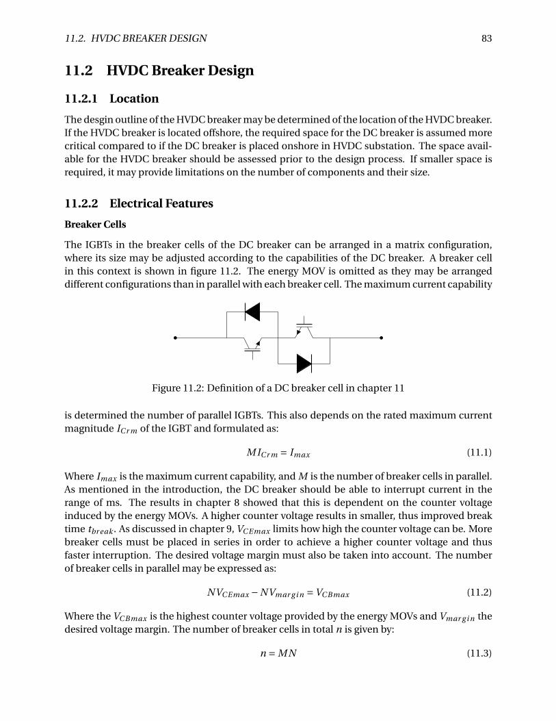
11.2. HVDC BREAKER DESIGN 83
11.2 HVDC Breaker Design
11.2.1 Location
The desgin outline of the HVDC breaker may be determined of the location of the HVDC breaker.If the HVDC breaker is located offshore, the required space for the DC breaker is assumed morecritical compared to if the DC breaker is placed onshore in HVDC substation. The space avail-able for the HVDC breaker should be assessed prior to the design process. If smaller space isrequired, it may provide limitations on the number of components and their size.
11.2.2 Electrical Features
Breaker Cells
The IGBTs in the breaker cells of the DC breaker can be arranged in a matrix configuration,where its size may be adjusted according to the capabilities of the DC breaker. A breaker cellin this context is shown in figure 11.2. The energy MOV is omitted as they may be arrangeddifferent configurations than in parallel with each breaker cell. The maximum current capability
Figure 11.2: Definition of a DC breaker cell in chapter 11
is determined the number of parallel IGBTs. This also depends on the rated maximum currentmagnitude ICr m of the IGBT and formulated as:
M ICr m = Imax (11.1)
Where Imax is the maximum current capability, and M is the number of breaker cells in parallel.As mentioned in the introduction, the DC breaker should be able to interrupt current in therange of ms. The results in chapter 8 showed that this is dependent on the counter voltageinduced by the energy MOVs. A higher counter voltage results in smaller, thus improved breaktime tbr eak . As discussed in chapter 9, VC Emax limits how high the counter voltage can be. Morebreaker cells must be placed in series in order to achieve a higher counter voltage and thusfaster interruption. The desired voltage margin must also be taken into account. The numberof breaker cells in parallel may be expressed as:
NVC Emax −NVmar g i n =VC Bmax (11.2)
Where the VC Bmax is the highest counter voltage provided by the energy MOVs and Vmar g i n thedesired voltage margin. The number of breaker cells in total n is given by:
n = M N (11.3)

84 CHAPTER 11. GUIDELINES FOR DC BREAKER DESIGN
Figure 11.3 illustrates the latest discussion with regard to the number of semiconductors re-quired for the main breaker of the hybrid topology.If the magnitude of the counter voltage provides a line voltage higher than the insulation co-
DC Breaker
Cell
DC Breaker
Cell
DC Breaker
Cell
DC Breaker
Cell
1/(Break time) [1/s]
Cu
rre
nt
bre
akin
g ca
pab
ility
[A
]
Figure 11.3: The relation between the properties of the DC breaker and the number of breakercells
ordination, there will be a risk of insulation breakdown. Secondary faults may be initiated. Themagnitude of the counter voltage is therefore limited by the insulation coordination VI .C . of theDC grid, expressed as:
VC Bmax <VI .C . (11.4)
The reliability of the DC breaker may increase with the number of breaker cells, but may aswell complicate the control system and demand space which is not available particularly in anoffshore location. Therefore, the type of IGBT should be considered in order to tolerate higherpower densities. For the ABB hybrid circuit breaker topology a Bi-mode Insulated Gate Transis-tor (BIGT) is suggested which is an integrated state of the art diode and IGBT solution [59].
Current Limiting Devices
In the experiments and in the design of the DC breaker for the NTNU/SINTEF lab, the effect ofthe line inductance Ll i ne is stressed. In case of short circuits with small Ll i ne , the current mayhave a steep rise, and the maximum breaking capability is exceeded due to the time responsetr esponse of the protection system. In figure 11.1, it is observed that the current will rise addition-ally due to the commutation from the nominal current path and into the main breaker. In order

11.2. HVDC BREAKER DESIGN 85
to avoid an unacceptable current rise, inserting a current limiting reactor (CLR) in series withthe DC line is suggested. In figure 2.7 a CLR is indicated. The reactor should provide sufficientinductance such that the current will not exceed the current breaking capability under currentinterruption. Assuming zero resistance and insignificant line inductance in fault current path,the minimum inductance of the limiter reactor LC LR needed may be expressed as:
LC LR ≤VDCtr esponse
Imax − Itr i p(11.5)
where Itr i p > Iload max
Where Il oad max is the estimated maximum load current under normal operation of the DC line.The trip level of the protection system Itr i p must be higher than Iload max in order to ensure thatthe DC breaker trips under faulted states of the DC grid only. In addition to a reactor, supercon-ducting fault current limiters are also suggested [4, 13].
Snubber Circuit
A snubber to protect the semiconductor may be essential for a DC breaker in order to avoidcomponent failure due to transient overvoltages. In the experimental work described in sec-tion 8.2.6, one of the effects of a higher capacitance was longer time of the counter voltage rise.The effect may thus contribute to delay the total fault clearance time. As the time is crucial forthe HVDC breaker operation, the capacitance of snubber may be too high. Investigating otheroptions to a pure capacitor snubber is recommended for HVDC breakers. E.g. using an MOVsnubber may provide the same protective properties [51]. The use of an MOV as a snubber mayprovide a faster voltage rise time of the counter voltage due to its non-linear resistive proper-ties. Other more complicated snubber circuits for the LCS for the hybrid topology is describedin [60]. These snubber configurations may also be an alternative for the main breaker as well.
Energy MOV
In section 9.5.2 the relation between the line inductance Ll i ne , the maximum energy dissipatedin the energy MOV WMOV max and the current capability were investigated. It was discussedthat the current breaking capability is limited by the number of energy MOVs. For the HVDCbreaker, the recommendation is to ensure sufficient WMOV max in order to dissipate the energycosponsoring to the maximum line inductance and the desired current breaking capability. Inthe theoretical background, a simplified approach to calculate the energy the DC breaker needsto dissipate was provided. Using equation 3.9 and assuming no resistance in the system and aconstant counter voltage, the requirement for WMOV max can be expressed as:
WMOV max ≥ 1
2(Ll i ne +LC LR )I 2
max(1+ VDC
(VC Bmax −VDC )) (11.6)
The energy MOVs can be arranged in different configurations. One configuration is similar tothe DC breaker in the NTNU/SINTEF lab with a parallel MOV for each DC breaker cell. It canbe assumed that the energy MOV contributes with a certain stray inductance, which is seen inthe equivalent circuit in figure 4.8. The electrical connection from the breaker cell to the en-ergy MOV may provide some stray inductance as well. Therefore, the energy MOVs should be

86 CHAPTER 11. GUIDELINES FOR DC BREAKER DESIGN
DC Breaker
Cell
DC Breaker
Cell
DC Breaker
Cell
Stray Inductance
Energy
MOVStray
Inductance
Energy
MOVStray
Inductance
Energy
MOV
(a) Energy MOV in parallel with each DC breaker cell
DC Breaker
Cell
DC Breaker
Cell
DC Breaker
Cell
Stray Inductance
Energy
MOV
(b) Energy MOV in parallel with three DC breaker cells
Figure 11.4: The relation between the configurations of energy MOVs and the stray inductance
arranged in a way the effect of stray inductance is minimised. Having energy MOVs for eachbreaker cell may contribute to increase the stray inductance. This is illustrated in figure 11.4a.Another solution with three breaker cells in series per energy MOV may reduce the stray induc-tances. This is illustrated in 11.4b. Also more than three breaker cells in series may be actual aslong as the voltage rating of the energy MOV is adjusted accordingly. However, the reliability ofthe DC breaker may decrease if the number of energy MOVs is minimised. If a energy MOV fails,the DC breaker may not to operate adequately if there are fewer and larger energy MOVs.
11.2.3 Control System and Thermal Features
In this section, the control system is referred to the internal DC breaker control system. The IG-BTs needs to be controlled by gate drivers, with typical gate emitter voltage VGE = 15 V. Operatinga DC-line in high voltage near the IGBT must be handled very carefully. As with the implemen-tation of the lab test model, galvanic isolation is needed to avoid ground potential contact withthe DC-line. Ground potential contact inside the high voltage parts of the DC breaker may alsobe regarded a fault in the DC grid, but also a DC breaker failure. Besides galvanic isolation in thecontrol system, the control system should have the minimum amount of time delay in order tominimise the response time.Similar to the DC breaker in the NTNU/SINTEF laboratory, thermal considerations will be partof the HVDC breaker design process. The nominal current will flow through the LCS and ac-tive cooling is assumed needed. The type of cooling medium should also be considered as theymay reduce the thermal heat resistivity further than with air-cooling fans. The analysis may bealso provided by more sophisticated software for thermal analysis, e.g thermal modelling in 3

11.2. HVDC BREAKER DESIGN 87
dimensions, in order to provide accurate results. Besides the semiconductors, the temperatureof the energy should be under surveillance to ensure that the HVDC breaker is able to dissipatethe energy in case of a fault.
11.2.4 Cost
The cost of the components should also be assessed in the design process. As the constructionof the DC breaker may have a limited budget, the HVDC breaker must be designed accordingly.E.g. the number of semiconductors in series may be reduced and a longer break time must betolerated.

88 CHAPTER 11. GUIDELINES FOR DC BREAKER DESIGN

Chapter 12
Discussion, Conclusion and Further work
12.1 Discussion and Conclusion
12.1.1 Theorethical Background
Chapters 2 to 5 were targeted at developing a theoretical background as a basis for the furtherwork in terms of simulations,the design process, developing guidelines and assembling a DCbreaker. The aspects of fault behaviour, current interruption, the components of a solid statebreaker were explained. The explanations were based on what is expected to be relevant inthe DC breaker design for the DC grid NTNU/SINTEF lab. Therefore, also simplifications werenecessary in order to limit the scope of work. E.g. the DC grid was represented by a fixed voltagesource with an inductor and a resistor, and semiconductor physics were very briefly considered.In order to analyse the results from the test model, design the final DC breaker, the theoreticalbackground was used and referred to in several occasions. E.g explaining the forcing of thecurrent to zero with the counter voltage and considerations of stray inductance. Also ratings ofboth the MOV and the IGBT were widely used in further chapters such as VC Emax was mentionedin order to avoid failure of the IGBT.
12.1.2 Test Model
Chapter 6 described the assembly of the test model, and chapter 8 presented the main resultfrom the experimental work with the test model. The test model was mainly used to examinethe electrical features and some particular thermal features of a solid state DC breaker. Theexperimental testing undertaken examined the different aspects of the operation of a solid statebreaker such as inductance, snubber and the source voltage. The interaction between the maincomponents, the energy MOV and the IGBT module, were stressed, as these are the componentswhich interaction forces the current to zero. The results also showed the advantages of fastcurrent interruption of the solid state breaker, as the break time was mainly under 1 ms. Thetemperature of the energy MOV was also examined; cooling characteristics and the heating dueto the repetitive short circuit. In chapter 9 it was assumed a 1 second time interval between therepetitive short circuit. A test with this time interval should also have been tested experimentallyin order to provide better predictions on the behaviour of the energy MOV due to repetitivecurrents. Also some leakage current tests could be undertaken. However, the result was able to
89

90 CHAPTER 12. DISCUSSION, CONCLUSION AND FURTHER WORK
provide the main aspects regarding the short circuit interruption which was considered as themain function of a DC breaker.
The results also showed some aspects regarding the measurement techniques. A rogowskicoil and LEM sensors provided accurate results for fast changing currents during the line currentcommutation from the IGBT and into the energy MOV. The current clamping meter used wasnot able to measure the fast changes in the current. The results measuring with a rogowski coilwere therefore eventually compared to the PSCAD simulations.
12.1.3 PSCAD Simulations
Chapter 7 described both the implementation of the test model and the final DC breaker inPSCAD. The simulations were presented in chapters 8 and 9. The PSCAD model of the testmodel needed adjustment since the preliminary result had unacceptable errors in the resultscompared to the experimental results from the test model. Therefore adjustment of the PSCADmodel were carried out according to the observations of the experimental results. Especially,the MOV was adjusted to its maximum expected voltage according to the 10 % tolerance band, acertain line resistance and stray inductance was added. The adjusted PSCAD simulations werein an acceptable range when compared to the experimental results. These experiences wereused when the final DC breaker model in PSCAD in order to ensure the validity of these results.In this model, the implementation had a conservative approach, in order to ensure the results.The simulation work was based on simplifications, and PSCAD simplifies the VI-characteristicof the semiconductors as linear. The assumptions of a capacitor snubber in the final designmitigating the overvoltage transients, allowed for more sufficient simulations as the time stepcould be increased.
An electro thermal equivalent circuit was also developed for the final DC breaker design. Asthe model assumes a one-dimensional heat transfer path, the values were used as an indicationand evaluated the need for a simple cooling fan. The thermal aspects have many dependencieswhich is not accounted for in the electro thermal model such as the movement of air aroundthe heat sink. The thermal resistance and the thermal time constant of the heat sink may subse-quently vary. Further investigations may be carried out in order to validate the results regardingthe thermal aspects of the DC breaker. For more accurate results, three-dimensional heat trans-fer simulation software may be used. This also may be actual for the thermal modelling of thevaristor.
12.1.4 DC Breaker Design
In chapter 9, the components for the final design were selected and the corresponding DCbreaker ratings were determined. Chapter 10 described the final configuration and the assemblyof the DC breaker for the NTNU/SINTEF lab.
The selection of components was based on a discussion on the corner cases and the exper-imental activities undertaken with the test model. The corresponding expected ratings of theDC breaker were determined with the help of manual calculations and PSCAD simulations. Inorder to ensure the calculations and simulations, the approach with the regard to selection ofcomponents was conservative. This was regarded as necessary as the calculations are basedupon assumptions and simplifications. A particular analysis of the line inductance in relation

12.1. DISCUSSION AND CONCLUSION 91
to maximum energy dissipated stressed the importance to considerer the line inductance whendesigning a DC breaker. For the repetitive current, the calculation conducted was not corre-sponding to what was observed in the test model. In the test model, the results indicated a hightolerance for repetitive currents of the energy MOV. This was not the case with the calculations.Temperature surveillance was therefore suggested in order to ensure if the DC breaker is readyfor current interruption, as the temperature should be under its critical level. An analysis of thelimitations of the components were also carried out, such as the rated expected voltage of theenergy MOV must not exceed the maximum tolerated voltage drop of the IGBT modules.
12.1.5 Design Guidelines
Chapter 11 described the development of design guidelines for HVDC circuit breakers, and theapproach was to put the experiences previously made in the context of HVDC applications. Thesolid state breaker was assumed the same function as the main breaker in hybrid HVDC breakertopology. It was stated that a realisation of a solid state DC breaker in HVDC grid would provideunacceptable losses. As the electrical features were investigated mostly in the theoretical back-ground, the test model and for the final DC breaker. However, some more general guidelinescould be made for the control system, thermal considerations, cost and reliability.
12.1.6 Main Conclusions
• A theoretical background was established and provided a basis for the rest of the work.
• The test model assembled provided insight of a solid state DC breaker operation and tothe design process with emphasis on the electrical features. The thermal experimentsundertaken may be improved to provide better insight of the thermal features of MOVs inDC breakers.
• The results from the test model illustrated that the interaction between a MOV and theIGBT is an essential aspect for the operation of DC circuit breakers. The interaction forcesthe current to zero by commutating the current and providing a counter voltage.
• A simplified PSCAD model was established and was used in order to design a DC breakerafter adjustments.
• A lab-scaled DC breaker was assembled. Still remains experimental validation and furthertesting.
• A DC breaker has design aspects as control system, thermal considerations, location andcost apart from the electrical aspects.
• Guidelines for a hybrid topology is possible to be carried out using insight from designinga solid state DC breaker

92 CHAPTER 12. DISCUSSION, CONCLUSION AND FURTHER WORK
12.2 Further Work
• Experimental validation of the electro thermal considerations of the semiconductors.
• Test the DC breaker for the ratings determined.
• Implementing temperature surveillance of the energy MOVs in the DC breaker.
• Further development of design guidelines for HVDC breakers in relation to experimentalactivities with the DC breaker assembled for NTNU/SINTEF lab.
• Use the bypass switch in the DC breaker to emulate the hybrid topology.
• Development of a protection system for the DC in the NTNU/SINTEF lab.
• Development of a distributed parameter line models for the DC grid in the NTNU/SINTEFlab in order to investigate a realistic interaction of a DC breaker with the DC grid.
• Develop electro-thermal models or 3-dimensional in PSCAD for the energy MOV for DCbreaker applications.

Appendix A
SIEMENS IGBT: BSM 300 GA 120 DN2
93


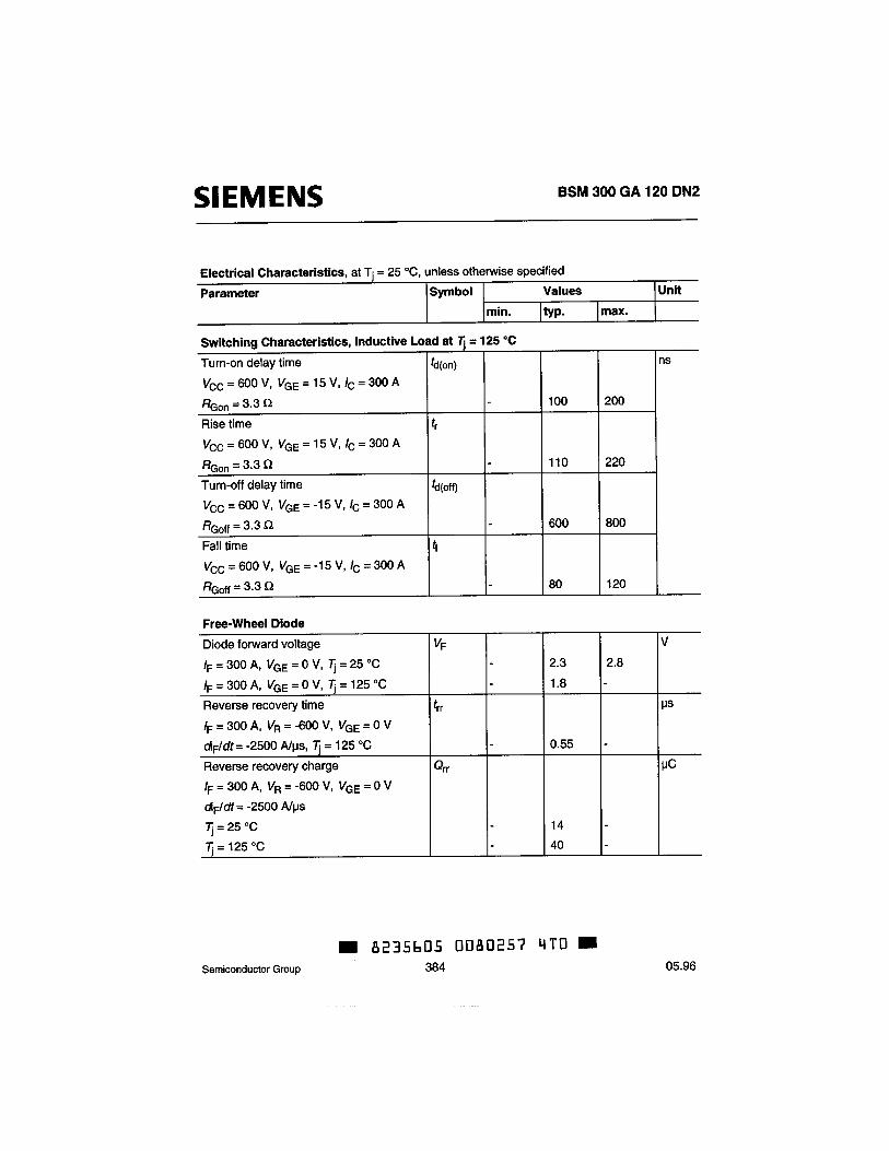


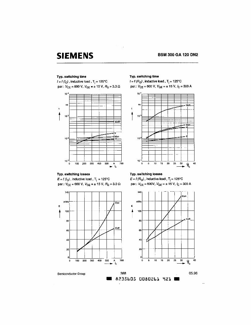

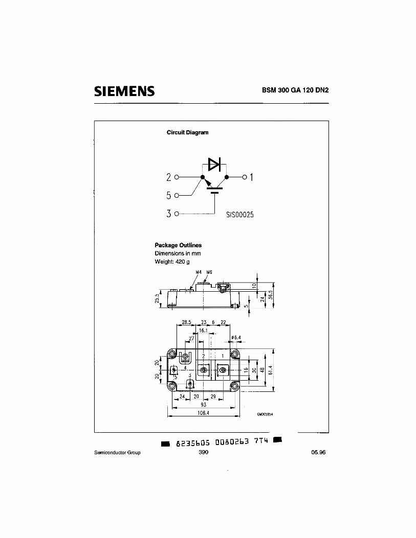


104 APPENDIX A. SIEMENS IGBT: BSM 300 GA 120 DN2

Appendix B
Time Delay of Contactor Switch
Time [ms]0 1 2 3 4 5 6 7 8 9 10
Curren
t[A
]
-0.2
-0.1
0
0.1
0.2
0.3
Voltage[V
]
0
200
400
600
800
1000
1200
Iswitch
Vswitch
10 · Vcoil
Figure B.1: Contactor switch operates with 0.15 A including the coil voltage
105

106 APPENDIX B. TIME DELAY OF CONTACTOR SWITCH
Time [ms]0 1 2 3 4 5 6 7 8 9 10
Curren
t[A
]
-0.2
-0.1
0
0.1
0.2
0.3
Voltage[V
]
0
200
400
600
800
1000
1200
Iswitch
Vswitch
300 · Vaux
Figure B.2: Contactor switch operates with 1 A including the auxiliary contact voltage
Time [ms]0 1 2 3 4 5 6 7 8 9 10
Curren
t[A
]
-1.6
-1.2
-0.8
-0.4
0
0.4
0.8
1.2
1.6
Voltage[V
]
0
200
400
600
800
1000
1200
1400
1600
Iswitch
Vswitch
10 · Vcoil
Figure B.3: Contactor switch operates with 1 A including the coil voltage

107
Time [ms]0 1 2 3 4 5 6 7 8 9 10
Curren
t[A
]
-1.6
-1.2
-0.8
-0.4
0
0.4
0.8
1.2
1.6
Voltage[V
]0
200
400
600
800
1000
1200
1400
1600
Iswitch
Vswitch
300 · Vaux
Figure B.4: Contactor switch operates with 1 A including the auxiliary contact voltage

108 APPENDIX B. TIME DELAY OF CONTACTOR SWITCH

Appendix C
Calculations
IGBT Module Power Loss
Infineon IGBT
Assumptions: VGE = 15 V and T j = 125 °CFrom the data sheet [54]: (V1, I1) = (1.12,100) and (V2, I2) = (1.64,300)
∆I
∆V= 200
0.52= 385.62 S
VC E (IC ) = IC
385.62+0.86
Infineon Anti-Parallel Diode
Assumptions: VGE = 15 V and T j = 125 °CFrom the data sheet [54]:(V1, I1) = (1,100) and (V2, I2) = (1.44,300)
∆I
∆V= 200
0.44= 454.55 S
VC E (IC ) = IC
454.55+0.78
Mitsubushi HVIGBT
Assumptions: VGE = 15 V and T j = 125 °CFrom the data sheet [53]: (V1, I1) = (2.7,100) and (V2, I2) = (4.1,300)
∆I
∆V= 300−100
4.1−2.7= 142.86 S
VC E (IC ) = IC
142.86+2.00
109

110 APPENDIX C. CALCULATIONS
Mitsubushi Anti-Parallel Diode
Assumptions: VGE = 15 V and T j = 125 °CFrom the data sheet [53]: (V1, I1) = (1.6,100) and (V2, I2) = (2.9,300)
∆I
∆V= 200
2.9−1.6= 153.85 S
VC E (IC ) = IC
153.85+0.95
Maxium Current with Respect to the Energy MOV
Energy MOV: V DC B60K460 EPCOS HighE series block varistorRated voltage:VMOV = 615 V DC[56]Assumtions: TMOV < Tcr i t i cal = 85°CFrom the VI-characteristic in data sheet VI-characteristic: (V1, I1) = (103,1400) and (V2, I2) =(104,1800)
α= ln104 − ln103
ln1800− ln1400= 9.16
KMOV = I2
V α2
= 1.52 ·10−26
I = KMOV V α = 5925.92 A

Appendix D
Snubber Capacitor Discharge
Time [ms]0 10 20 30 40 50 60 70 80 90 100
Curren
t[A
]
0
100
200
300
400
500
600
Voltage[V
]
0
300
600
900
1200
1500
1800
IlineVDCCB
VCE
Figure D.1: Current interruption and discharge of the snubber
111

112 APPENDIX D. SNUBBER CAPACITOR DISCHARGE
Time [ms]0 50 100 150 200 250 300 350 400 450 500
Curren
t[A
]
0
100
200
300
400
500
600
Voltage[V
]0
300
600
900
1200
1500
1800
IlineVDCCB
VCE
Figure D.2: Current interruption and discharge of the snubber

Appendix E
Maximum Current Breaking Capability
Line inductance Lline [mH]10-2 10-1 100 101 102
Current[pu]
0
2
4
6
8
10
12
14
Imax
Itrip
Figure E.1: The current breaking capability Imax as a function line inductance Ll i ne , Imax is theactual current interrupted and Itr i p is the maximum detection level of the protection system,tr esponse = 1 ms
113
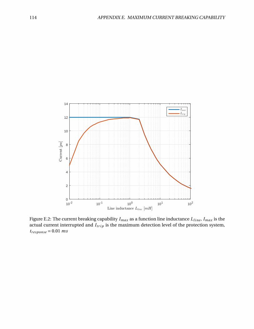
114 APPENDIX E. MAXIMUM CURRENT BREAKING CAPABILITY
Line inductance Lline [mH]10-2 10-1 100 101 102
Current[pu]
0
2
4
6
8
10
12
14
Imax
Itrip
Figure E.2: The current breaking capability Imax as a function line inductance Ll i ne , Imax is theactual current interrupted and Itr i p is the maximum detection level of the protection system,tr esponse = 0.01 ms

115
Line inductance Lline [mH]10-2 10-1 100 101 102
Current[pu]
0
2
4
6
8
10
12
14
Imax
Itrip
Figure E.3: The current breaking capability Imax as a function line inductance Ll i ne , Imax is theactual current interrupted and Itr i p is the maximum detection level of the protection system,tr esponse = 0.0001 ms

116 APPENDIX E. MAXIMUM CURRENT BREAKING CAPABILITY

Appendix F
DC breaker circuit diagrams
117

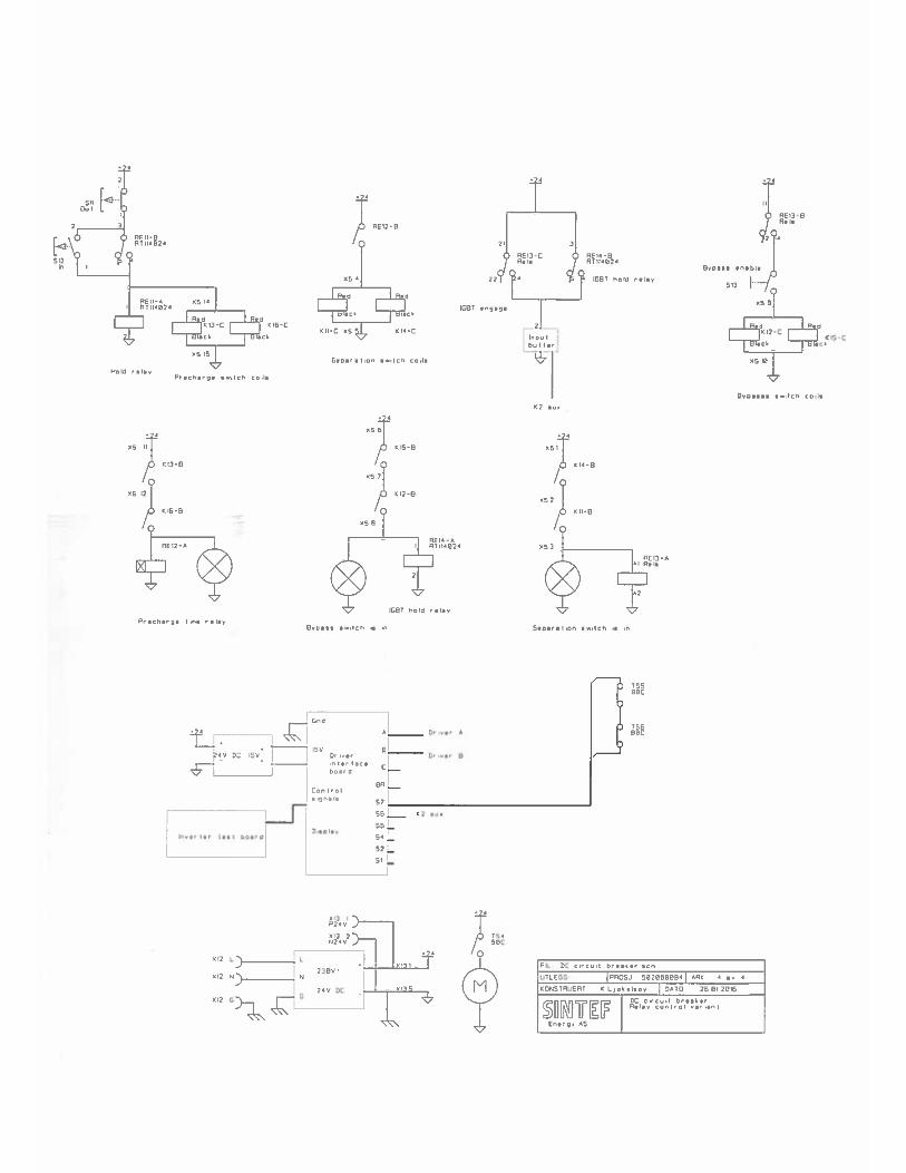


Bibliography
[1] E. O. Norum, “Protection system for dc grid applications,” Dec 2014, specialization project,NTNU.
[2] C. Franck, “Hvdc circuit breakers: A review identifying future research needs,” Power De-livery, IEEE Transactions on, vol. 26, no. 2, pp. 998–1007, Apr 2011.
[3] D. V. Hertem and M. Ghandhari, “Multi-terminal vsc hvdc for the european supergrid: Ob-stacles,” Renewable and Sustainable Energy Reviews, vol. 14, no. 9, pp. 3156 – 3163, 2010.
[4] WG.B4.52, “Hvdc grid feasibility study,” CIGRE, Technical Brochure, Apr 2013.
[5] M. Callavik, A. Blomberg, J. Häfner, and B. Jacobson, “The hybrid hvdc breaker,” ABB GridSystems Tech. Paper, 2012.
[6] R. Adapa, “High-wire act: Hvdc technology: The state of the art,” Power and Energy Maga-zine, IEEE, vol. 10, no. 6, pp. 18–29, Nov 2012.
[7] C. Davidson, R. Whitehouse, C. Barker, J.-P. Dupraz, and W. Grieshaber, “A new ultra-fasthvdc circuit breaker for meshed dc networks,” in AC and DC Power Transmission, 11th IETInternational Conference on, Feb 2015, pp. 1–7.
[8] G. Reed, B. Grainger, A. Sparacino, and Z.-H. Mao, “Ship to grid: Medium-voltage dc con-cepts in theory and practice,” Power and Energy Magazine, IEEE, vol. 10, no. 6, pp. 70–79,Nov 2012.
[9] B. Andersen. (2014) Cigre sc b4 activities towards hvdc grids. CI-GRE. [Online]. Available: http://b4.cigre.org/Publications/Other-Documents/SC-B4-presentations-and-papers/Cigre-SC-B4-Activities-Towards-HVDC-Grids
[10] M. Bahrman and B. Johnson, “The abcs of hvdc transmission technologies,” Power andEnergy Magazine, IEEE, vol. 5, no. 2, pp. 32–44, Mar 2007.
[11] J. Sneath and A. Rajapakse, “Dc fault protection of a nine-terminal mmc hvdc grid,” in ACand DC Power Transmission, 11th IET International Conference on, Feb 2015, pp. 1–8.
[12] D. P. W. Grieshaber, J.P. Dupraz and L. Violleau, “Development and test of a 120 kv directcurrent circuit breaker,” in Cigre Session 2014, 2014.
[13] R. E. Torres-Olguin and J. I. Marvik, “Review of protection systems for dc grids,” SINTEFEnergy Research, Project memo AN. 13.12.39, Jun 2013.
121

122 BIBLIOGRAPHY
[14] M. K. Bucher, “Transient fault currents in hvdc vsc networks during pole-to-ground fault,”Ph.D. dissertation, ETH-Zurich, 2014.
[15] M. Bucher, M. Walter, M. Pfeiffer, and C. Franck, “Options for ground fault clearance inhvdc offshore networks,” in Energy Conversion Congress and Exposition (ECCE), 2012 IEEE,Sept 2012, pp. 2880–2887.
[16] A. Shukla and G. Demetriades, “A survey on hybrid circuit-breaker topologies,” Power De-livery, IEEE Transactions on, vol. 30, no. 2, pp. 627–641, Apr 2015.
[17] A. Bissal, “Modeling and verification of ultra-fast electro-mechanical actuators for hvdcbreakers,” Ph.D. dissertation, KTH, 2015.
[18] T. Eriksson, M. Backman, and S. Halen, “A low loss mechanical hvdc breaker for hvdc gridapplications,” in Cigre Session 2014, 2014.
[19] J. William H. Hayt and J. A. Buck, Engineering Electromagnetics, 6th ed. McGraw-Hill, 2001.
[20] M. Runde, Current Interruption in Power Grids. NTNU, 2015.
[21] J.-B. Curis, “Testing results from dc network mock-up and dc breaker prototype,” Twenties,http://www.twenties-project.eu/node/18, Tech. Rep., 2013.
[22] R. Derakhshanfar, T. Jonsson, U. Steiger, and M. Habert, “Hybrid hvdc breaker technologyand applications in point-to-point connections and dc grids,” CIGRE, Tech. Rep., 2014.
[23] J. Arrillaga, Y. Liu, and N. Watson, Flexible Power Transmission: The HVDC Options. Wiley,2007.
[24] V. K. Khanna, IGBT Fundamentals and Status Review. Wiley-IEEE Press, 2003.
[25] N. Mohan, T. Undeland, and W. Robbins, Power electronics: Converters, Applications, andDesign. John Wiley & Sons, 2003.
[26] B. Baliga, M. S. Adler, R. Love, P. Gray, and N. Zommer, “The insulated gate transistor: A newthree-terminal mos-controlled bipolar power device,” Electron Devices, IEEE Transactionson, vol. 31, no. 6, pp. 821–828, Jun 1984.
[27] S. Abedinpour and K. Shenai, “5 - insulated gate bipolar transistor,” in PowerElectronics Handbook (Second Edition), second edition ed., ser. Engineering, M. H.Rashid, Ed. Burlington: Academic Press, 2007, pp. 71 – 88. [Online]. Available:http://www.sciencedirect.com/science/article/pii/B9780120884797500237
[28] A. Wintrich, U. Nicolai, W. Tursky, and T. Reimann, “Application manual power semicon-ductors,” SEMIKRON International GmbH, Tech. Rep., 2015, availible 31.10.2015. [On-line]. Available: http://www.semikron.com/dl/service-support/downloads/download/semikron-application-manual-power-semiconductors-english-en-2015
[29] L. M. Levinson and H. R. Philipp, “Metal oxide varistor a multijunction thin-film device,”Applied Physics Letters, vol. 24, no. 2, pp. 75–76, 1974.

BIBLIOGRAPHY 123
[30] H. K. Høidalen, Overspenninger og overspenningsvern. NTNU, 2013.
[31] SIOV metal oxide varistors, General technical information, EPCOS AG, Apr 2011. [Online].Available: http://de.tdk.eu/blob/185716/download/3/siov-general.pdf
[32] E. Kuffel, W. Zaengl, and J. Kuffel, High Voltage Engineering Fundamentals. Newnes, 2000.
[33] P. Pinceti and M. Giannettoni, “A simplified model for zinc oxide surge arresters,” PowerDelivery, IEEE Transactions on, vol. 14, no. 2, pp. 393–398, Apr 1999.
[34] WG.A3.17, “Mo surge arresters stresses and test procedures,” CIGRE, Technical Brochure,Aug 2013.
[35] V. Hinrichsen, M. Reinhard, and B. Richter, “Energy handling capability of high-voltagemetal-oxide surge arresters part 1: a critical review of the standards,” in Cigre InternationalTechnica l Colloquium. CIGRE, Sep 2007.
[36] M. Fasching, “Effects of stray inductance on switching transients of an igbt propulsion in-verter and resulting gate control strategies,” in AFRICON, 1996., IEEE AFRICON 4th, vol. 1,Sep 1996, pp. 467–472 vol.1.
[37] R. Chokhawala and S. Sobhani, “Switching voltage transient protection schemes for high-current igbt modules,” Industry Applications, IEEE Transactions on, vol. 33, no. 6, pp. 1601–1610, Nov 1997.
[38] J. Magnusson, R. Saers, L. Liljestrand, and G. Engdahl, “Separation of the energy absorptionand overvoltage protection in solid-state breakers by the use of parallel varistors,” PowerElectronics, IEEE Transactions on, vol. 29, no. 6, pp. 2715–2722, Jun 2014.
[39] AN2008-03 Thermal equivalent circuit models, 2008th ed., Infineon Technologies AG, Jun2008. [Online]. Available: http://www.infineon.com/dgdl/Infineon-AN2008_03_Thermal_equivalent_circuit_models-AN-v1.0-en.pdf?fileId=db3a30431a5c32f2011aa65358394dd2
[40] R. Pittini, S. D’Arco, M. Hernes, and A. Petterteig, “Thermal stress analysis of igbt modulesin vscs for pmsg in large offshore wind energy conversion systems,” in Power Electronicsand Applications (EPE 2011), Proceedings of the 2011-14th European Conference on, Aug2011, pp. 1–10.
[41] (2015, Desember) Renewable energy system laboratory. SINTEF En-ergy Research. [Online]. Available: https://www.sintef.no/en/all-laboratories/renewable-energy-system-laboratory/
[42] K. Ljøkelsøy, S. D’Arco, and J. O. Tande, “Challenges and rationale for laboratory researchof offshore grids,” Energy Procedia, vol. 24, pp. 237 – 244, 2012.
[43] K. Ljøkelsøy, “60 kva laboratory converter unit.documentation. issue 2,” SINTEF EnergyResearch, Project memo AN 11.12.10, Nov 2014.
[44] K. Ljøkelsøy and T. Rogne, “Gatedriver smd2,” SINTEF Energy Research, Project memo AN01.12.17, Jun 2001.

124 BIBLIOGRAPHY
[45] K. Ljøkelsøy and R. Lund, “Driver interface board, v 4.0 - documentation,” SINTEF EnergyResearch, Project memo AN 00.12.49, Nov 2000.
[46] K. Ljøkelsøy, “Vekselretter testkort v1:0. beskrivelse,” SINTEF Energy Research, Projectmemo AN 09.12.12, Feb 2009.
[47] KILOVAC EV200 Series Contactor With 1 Form X (SPST-NO) Contacts Rated 500+Amps, 12-900 Vdc, TE Connectivity Ltd, Mar 2013. [Online]. Available: http://www.te.com/commerce/DocumentDelivery/DDEController?Action=showdoc&DocId=Catalog+Section%7F5-1773450-5_sec7_EV200A%7F0313%7Fpdf%7FEnglish%7FENG_CS_5-1773450-5_sec7_EV200A_0313_._5-1773450-5_Sec7_EV200A.pdf%7F1618002-1
[48] J.-R. Riba, A. Garcia, J. Cusido, and M. Delgado, “Dynamic model for ac and dc contac-tors simulation and experimental validation,” Simulation Modelling Practice and Theory,vol. 19, no. 9, pp. 1918 – 1932, 2011.
[49] N. Watson and J. Arrillaga, IET Power and Energy Series, Volume 39 - Power Systems Electro-magnetic Transients Simulation. Institution of Engineering and Technology, 2007.
[50] J. Magnusson, “On the design of hybrid dc-breakers consisting of a mechanical switch andsemiconductor devices,” Master’s thesis, KTH, 2015.
[51] J. Magnusson, A. Bissal, G. Engdahl, R. Saers, Z. Zhang, and L. Liljestrand, “On the use ofmetal oxide varistors as a snubber circuit in solid-state breakers,” in Innovative Smart GridTechnologies Europe (ISGT EUROPE), 2013 4th IEEE/PES, Oct 2013, pp. 1–4.
[52] SIOV metal oxide varistors - Leaded varistors, StandarD series, EPCOS AG, Dec 2011.[Online]. Available: http://en.tdk.eu/inf/70/db/var_11/SIOV_Leaded_StandarD.pdf
[53] MITSUBISHI HVIGBT MODULES, CM400DY-66H, Mitsubishi Electric Corporation, Mar2003. [Online]. Available: http://www.mitsubishielectric.com/semiconductors/content/product/powermod/powmod/hvigbtmod/hvigbt/cm400dy-66h_e.pdf
[54] Technical Information IGBT Modue FZ600R17KE3, Infineon Technologies AG, Oct 2013.[Online]. Available: http://www.infineon.com/dgdl/Infineon-FZ600R17KE3-DS-v03_00-en_de.pdf?fileId=db3a304412b407950112b43044fb4fda
[55] (2016, Jan) Standard extruded heatsinks. [Online]. Available: http://www.fischerelektronik.de/web_fischer/en_GB/heatsinks/A01/Standard%20extruded%20heatsinks/PR/SK435_/$productCard/parameters/index.xhtml
[56] SIOV metal oxide varistors, Block varistors, HighE series, EPCOS AG, Apr 2011. [Online].Available: http://en.tdk.eu/inf/70/db/var_11/SIOV_Block_HighE.pdf
[57] T. K. Vrana, Y. Yang, D. Jovcic, S. Dennetiere, J. Jardini, and H. Saad, “The cigre b4 dc gridtest system,” ELECTRA, no. 270, pp. 10–19, Oct 2013.
[58] P. Skarby and U. Steiger, “An ultra-fast disconnecting switch for a hybrid hvdc breaker, atechnical breakthrough,” in 2013 CIGRE Canada Conference. CIGRE, 2013.

BIBLIOGRAPHY 125
[59] M. Rahimo, A. Kopta, U. Schlapbach, J. Vobecky, R. Schnell, and S. Klaka, “The bi-modeinsulated gate transistor (bigt) a potential technology for higher power applications,” inPower Semiconductor Devices IC’s, 2009. ISPSD 2009. 21st International Symposium on,June 2009, pp. 283–286.
[60] A. Hassanpoor, J. Hafner, and B. Jacobson, “Technical assessment of load commutationswitch in hybrid hvdc breaker,” Power Electronics, IEEE Transactions on, vol. 30, no. 10, pp.5393–5400, Oct 2015.