design and modeling of nanodevices
TRANSCRIPT

NM6605 NTU–TUM
X. ZHOU 1 © 2020
NM6605: Design and Modeling of Nanodevices
Design and Modeling of NanodevicesCompact Modeling of Nano MOSFETs
Design and Modeling of NanodevicesCompact Modeling of Nano MOSFETs
Dr Zhou Xing
Web: https://www.ntu.edu.sg/home/exzhou/Teaching/TUM-NM6605/
Office: S1-B1c-95Phone: 6790-4532Email: [email protected]
NM6605 NTU–TUM
X. ZHOU 2 © 2020
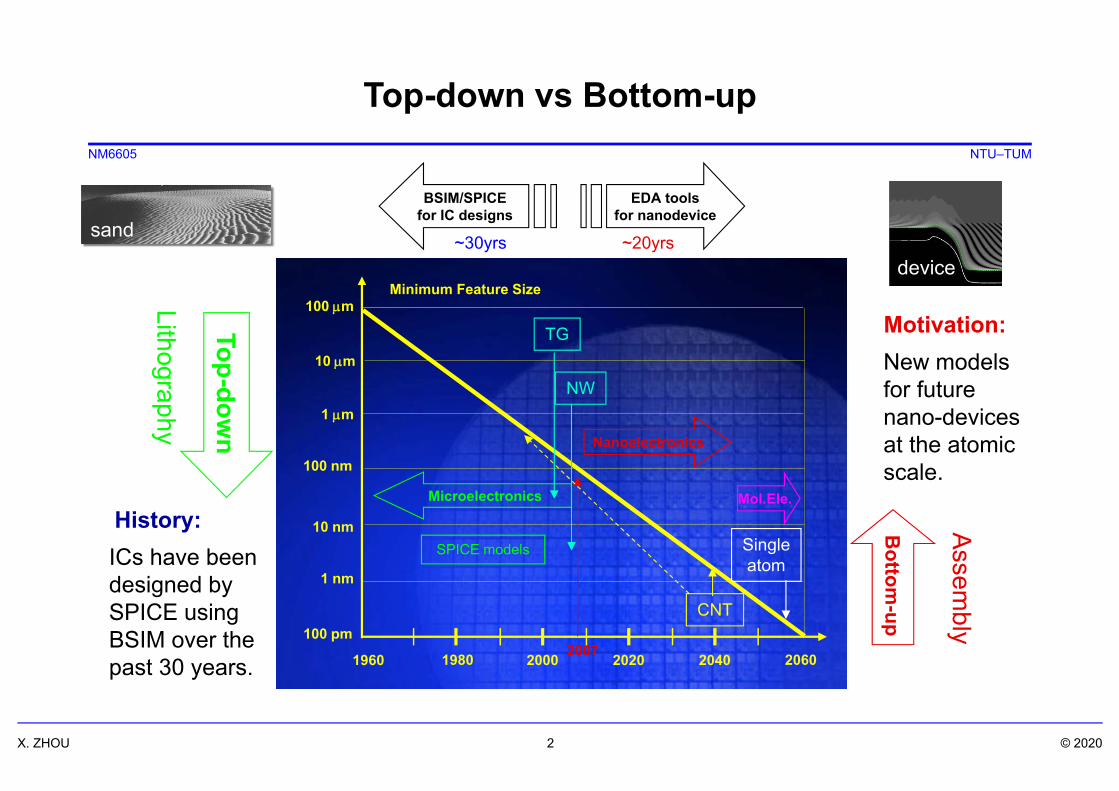
Top-down vs Bottom-up
Top-down
Bottom
-up
Lithography
Assembly
Motivation:New models for future nano-devices at the atomic scale.
History:ICs have been designed by SPICE using BSIM over the past 30 years.
sand
device~20yrs~30yrs
EDA toolsfor nanodevice
BSIM/SPICEfor IC designs
100 m
10 m
1 m
100 nm
10 nm
1 nm
100 pm
1960 2060202020001980 2040
CNT
Singleatom
2007
Nanoelectronics
Microelectronics Mol.Ele.
Minimum Feature Size
SPICE models
NW
TG

NM6605 NTU–TUM
X. ZHOU 3 © 2020
M. Chan, et al., Microelectronics Reliability, vol. 43, pp. 399-404, 2003.
A disturbing version of “Moore’s law” — the number of compact-model parameters doubles about every decade (as a result of “evolutionary” development)
“Moore’s Law”
Compact Model Parameters
Chip complexity will double about every 18 months.

NM6605 NTU–TUM
X. ZHOU 4 © 2020
Approaches to Analyzing Microelectronic Systems

NM6605 NTU–TUM
X. ZHOU 5 © 2020
Process/structural variations
Device
Process
Gate
Block
Centered at transistor-level compact model
Parameterextraction
Analogand
Digitalacceleration
Subcircuitexpansion
Transistor optimization
System performance
MotivationCompact multi-level
technology/transistor/subsystem modeling
Technology development
Circuit
Interconnect
Process effectson device/circuit
Process – Device – Circuit – Block – System
NM6605 NTU–TUM
X. ZHOU 6 © 2020
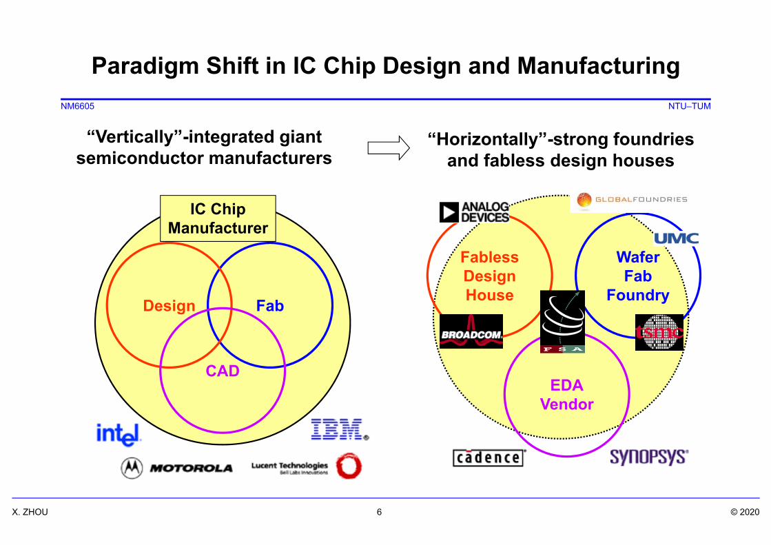
“Vertically”-integrated giant semiconductor manufacturers
“Horizontally”-strong foundries and fabless design houses
FabDesign
CAD
IC ChipManufacturer
WaferFab
Foundry
FablessDesignHouse
EDAVendor
Paradigm Shift in IC Chip Design and Manufacturing

NM6605 NTU–TUM
X. ZHOU 7 © 2020
Ideality
SPICESPICE
Reality
EDA Vendor
CAD developer
Design House
Circuit designer
Wafer Fab
Process engineerCM
Model developer
Design–Fabrication Paradigm: Ideality & Reality

NM6605 NTU–TUM
X. ZHOU 8 © 2020
Wafer FabDesign House
EDA Vendor
CAD developer
Circuit designer Process engineerCM
Model developer
I won’t extract your model unless my customer
(designer) wants it…
I won’t use it unless it’s been implemented in
my SPICE simulator…
I won’t code it unless fab can provide data and model…
Do you want to trymy new model?
Will you supportmy new model?
Can you implementmy new model?
1 32
Model Developer’s Dilemma

NM6605 NTU–TUM
X. ZHOU 9 © 2020
Models and Modeling Groups
BSIM EKV HiSIM ULTRA-SOI/MGACM
NGSOI/MG Model
Xsim Technology-dependent predictive model DG/MG SiNW/CNT PCMOSISNE
III-V/Si

NM6605 NTU–TUM
X. ZHOU 10 © 2020
’70 ’80 ’90 ’00Time
Accuracy & Speed
’10
Central concern for CM: accuracy–speed tradeoff
Vt-based
s-based
P–S M1 M2 M3 B1 B2 B3
SPM11HiS
M9B4
SPP
EKV
Qi-based
U
Determined by demand/supply
X
(No demand for 30+ yrs)
(Not as slow with HPC)
Iterative: can be costly for digital
(High demand for analog)
ACM
B5
PSP
Future: how to tradeoff?
• Scalable (non-binnable): accuracy over geometry
• Single-piece across all regions• Selectable accuracy within the
same core model• Extension to non-bulk FETs
Accuracy–Speed Tradeoff: History & Future

NM6605 NTU–TUM
X. ZHOU 11 © 2020
Role of Compact Model
(Courtesy: M. Chan) Ultimate goal: towards accuracy and simplicity

NM6605 NTU–TUM
X. ZHOU 12 © 2020
f(x)
x
x0 x1x2
x3
1
1 2
1 1
01 2 2 1
21 1
2 2 3
1 1 2 1 2
1 2 1 1 2C
C C
C CI iR R h R h Vi iVC C
R h R R h
Transient:“companion”
1 11 2 2 1 0
21 1
2 2 3
1 1 1
1 1 1 0
jj C j C
R R R V I eVj C j C
R R R
AC:
1 2 01 2 2
1 22 2 3
1 1 1
1 1 1 0
V V IR R R
V VR R R
KVL/KCL:
1 2 2 1 0
2
2 2 3
1 1 1
1 1 1 0R R R V I
VR R R
DC:
1 '
nn n
n
f xx x
f x
Nonlinear: N–R iteration
0 1thV nvI I e
SPICE Circuit Simulation: (Modified) Nodal Analysis

NM6605 NTU–TUM
X. ZHOU 13 © 2020
What Is a Model, and Modeling?
“The sciences do not try to explain, they hardly even try to interpret, they mainly make models. By a model is meant a mathematical construct which, with the addition of certain verbal interpretations, describes observed phenomena. The justification of such a mathematical construct is solely and precisely that it is expected to work.”
John von Neumann
A model is a mental image of reality
• One can have many different images of the same reality.• Correct physical approximations and correct mathematical
formulations to emulate ideal device physical behaviors and corroborate with real device characteristics.
• What does “compact” mean?• What is “physical” of a model?

NM6605 NTU–TUM
X. ZHOU 14 © 2020
ID(V) = Ids + Ib + IgMonte Carlo:(6-D, t)
ID(k,r,t)t
rk
Numerical:(3-D, t)
ID(r,t,)t
r(x,y,z)
Compact: (0-D, t)
ID
Ids
Ib
IgDGS
B
“DC”(n sets = “unphysical”)
Q + Q(t)
f, (t)
Vg,Vd,Vb,VsL,W,(Z)
Age
T
QI = Qv
Gij = Ii/Vj
Cij = Qi/Vj
SPICE(nodal analysis)
mental image
Perspective: Compact Modeling for Circuit Simulation
NM6605 NTU–TUM
X. ZHOU 15 © 2020
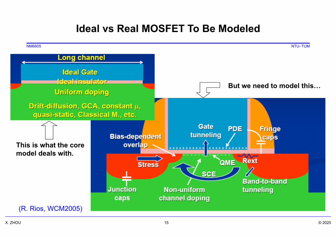
Ideal vs Real MOSFET To Be Modeled
(R. Rios, WCM2005)
This is what the core model deals with.
But we need to model this…
NM6605 NTU–TUM
X. ZHOU 16 © 2020
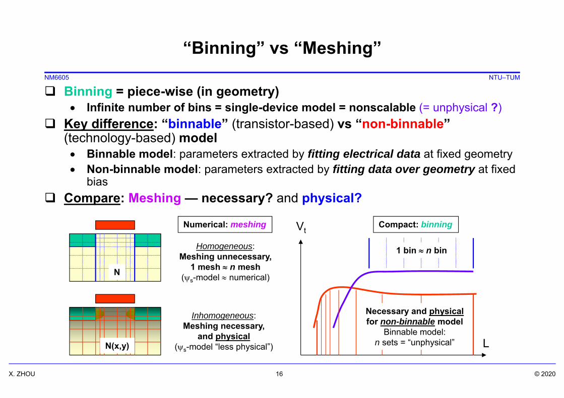
Binning = piece-wise (in geometry) Infinite number of bins = single-device model = nonscalable (= unphysical ?)
Key difference: “binnable” (transistor-based) vs “non-binnable” (technology-based) model Binnable model: parameters extracted by fitting electrical data at fixed geometry Non-binnable model: parameters extracted by fitting data over geometry at fixed
bias Compare: Meshing — necessary? and physical?
L
Vt
N
N(x,y)
Numerical: meshing
Homogeneous:Meshing unnecessary,
1 mesh n mesh(s-model numerical)
Inhomogeneous:Meshing necessary,
and physical(s-model “less physical”)
Compact: binning
Necessary and physicalfor non-binnable model
Binnable model:n sets = “unphysical”
1 bin n bin
“Binning” vs “Meshing”
NM6605 NTU–TUM
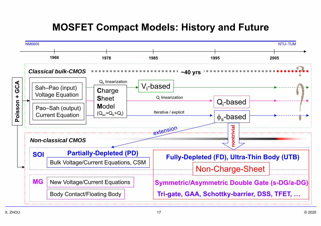
X. ZHOU 17 © 2020
Sah–Pao (input)Voltage Equation
Pao–Sah (output)Current Equation s-based
Qi-based
Vt-basedQb linearization
Qi linearization
Iterative / explicit
1966 1978 1985 1995 2005
Pois
son
+ G
CA
Classical bulk-CMOS
ChargeSheetModel(Qsc=Qb+Qi)
~40 yrs
MOSFET Compact Models: History and Future
Non-classical CMOS
SOI
MG
Bulk Voltage/Current Equations, CSM
New Voltage/Current Equations
Partially-Depleted (PD) Fully-Depleted (FD), Ultra-Thin Body (UTB)
Non-Charge-SheetSymmetric/Asymmetric Double Gate (s-DG/a-DG)
nont
rivia
l
Tri-gate, GAA, Schottky-barrier, DSS, TFET, …Body Contact/Floating Body
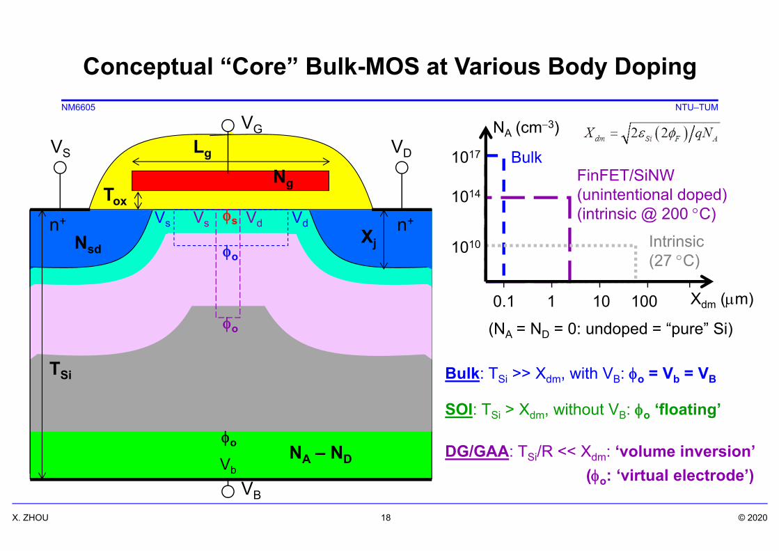
NM6605 NTU–TUM
X. ZHOU 18 © 2020
Conceptual “Core” Bulk-MOS at Various Body Doping
VGVS VD
VB
Vs
Vb
VdVs Vdn+ n+
NA – ND
NsdXj
Ng
Lg
Tox
TSi
NA (cm3)
Xdm (m)
1017
1014
1010
0.1 1 10010
s
o
o
o
BulkFinFET/SiNW(unintentional doped)(intrinsic @ 200 C)
Intrinsic(27 C)
(NA = ND = 0: undoped = “pure” Si)
Bulk: TSi >> Xdm, with VB: o = Vb = VB
SOI: TSi > Xdm, without VB: o ‘floating’
DG/GAA: TSi/R << Xdm: ‘volume inversion’(o: ‘virtual electrode’)

NM6605 NTU–TUM
X. ZHOU 19 © 2020
Need for an Extendable Core Model for Future Generation
Bulk PD-SOI FD-UTB/SOI DG/GAA/SB/DSS
ID
Ids
DGS
B
(B)
Sub
IDDGS
DG1S
G2
ID
Sub
DGSID
Vt-based models
Time’60 ’70 ’80 ’90 ’00 ’10
Qi-based modelss-based models
Pao–Sah
History has witnessed generations of MOS modelsand efforts required from one generation to the next …
— Need for a core model extendable to future generations,and with less duplicating efforts
MG/FinFET is just a special case
HEMT – leveraging on MOS models

NM6605 NTU–TUM
X. ZHOU 20 © 2020
Vg
Vs Vd
Vb
(a)
PD-SOI
toxf
tSi
oxf
oxb toxb
s
b
0
Vg
Vs Vd
Vb
(b)
FD-UTB/SOI
Vg
Vs Vd
Vb
(c)
a-DG
Vg
Vs Vd
Vg
(d)
s-DG
Vg
Vs Vd
(e)
'Bulk-UTB'
Vg
Vs Vd
Vb
(f)
Bulk
Vb = Vg
toxb = toxftSi
half s-DGtSi
toxb '0 = 0
0 0'
b 0b = 0
b 0 'b 0
'0 = 0
s = b
PD-SOI FD-UTB/SOI a-DG s-DG UTB Bulk
'b = 0
b = 0
Seamless Transformation and Unification of MOSFETs

NM6605 NTU–TUM
X. ZHOU 21 © 2020
The Generic SOI/DG/GAA MOSFET
Common/symmetric-DG [GAA] Vg1 = Vg2 = Vg: two gates with one bias Cox1 = Cox2: s-DG (Xo = TSi/2; [R]) Full-depletion: VFD = Vg(Xd=TSi/2) Cox1 Cox2: ca-DG (Xo < TSi)
Independent/asymmetric-DG Vg1 Vg2: ia-DG, biased independently Zero-field location may be outside body Consider two “independent” gates; linked
through full-depletion condition:
Unification of MOS
Zero-field potential: o [o'(Xo) = 0]
Imref-split: Vcr = Fn – Fp = Vc – Vr
Vr = Vb (BC: body-contacted)Vr = Vmin = min(Vs, Vd) (“FB”: w/o BC)
Bulk: special case of s-DG SOI: special case of ia-DG
Xd1 + Xd2 = TSi
GAA
• SOI ia-DG ca-DG s-DG bulk
NM6605 NTU–TUM
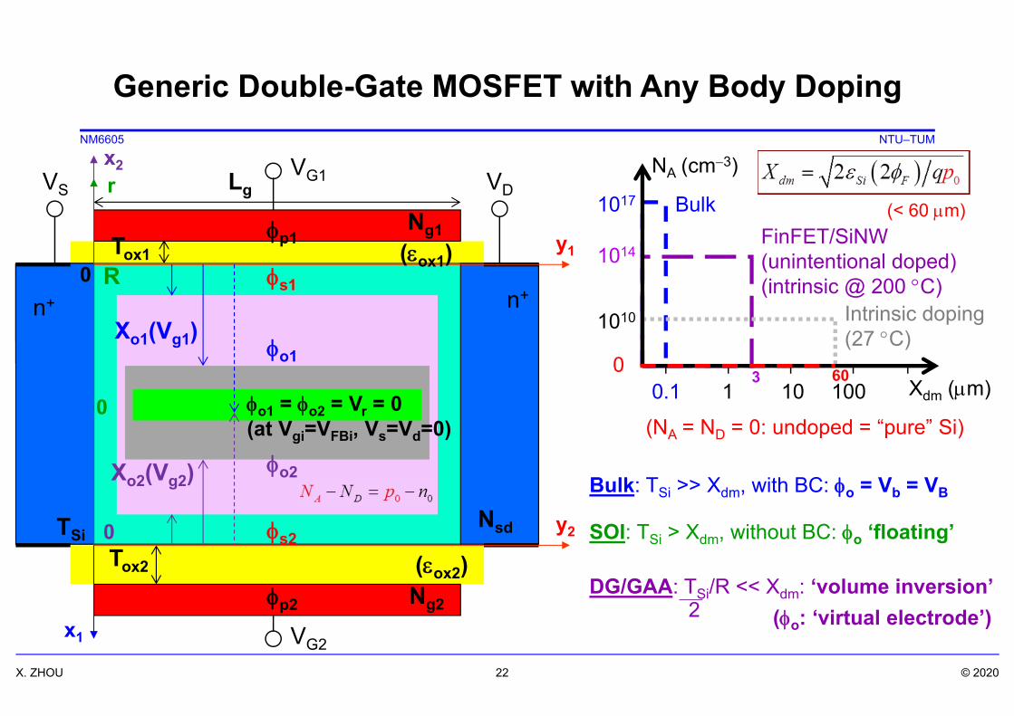
X. ZHOU 22 © 2020
Generic Double-Gate MOSFET with Any Body Doping
VG1VS VD
Ng1
Lg
Tox1s1
o1
n+
TSiNsd
0
0
x1
y1
R
r
n+
Tox2
s2
o1 = o2 = Vr = 0 (at Vgi=VFBi, Vs=Vd=0)
VG2
Xo1(Vg1)
x2
0
o2Xo2(Vg2)
Ng2
y2
p1
p2
(ox2)
NA (cm3)
Xdm (m)
1017
1014
1010
0.1 1 10010
BulkFinFET/SiNW(unintentional doped)(intrinsic @ 200 C)
Intrinsic doping(27 C)
(NA = ND = 0: undoped = “pure” Si)
Bulk: TSi >> Xdm, with BC: o = Vb = VB
SOI: TSi > Xdm, without BC: o ‘floating’
DG/GAA: TSi/R << Xdm: ‘volume inversion’(o: ‘virtual electrode’)2
(ox1)
0
(< 60 m)
3 60

NM6605 NTU–TUM
X. ZHOU 23 © 2020
PD/FD at Various Body Doping/Thickness
VGVS = 0 VD = 0
Ng
Lg
Tox
NA – ND(cm–3)
s
o
o
n+
TSi
Nsd
0
x
n+
Kox
s
o = Vr = 0 @ VG=VFB, VS=VD=0
VG
Xdm
TSi2
o
1018
1014
1017
y
VGVS = 0 VD = 0
n+ n+
TSi2
PD
VGVS = 0 VD = 0
n+ n+TSi2
Xdmo FDs
1018
sXdm
o PD
o FD1017

NM6605 NTU–TUM
X. ZHOU 24 © 2020
Dynamic Depletion (DD) at Various Body Thickness
VGVS = 0 VD = VDD
Ng
Lg
Tox
NA – ND(1017 cm–3)
sn+
TSi
Nsd
0
x
y
n+
Kox
s
VG
TSi2
VGVS = 0 VD = VDD
n+ n+TSi2
o
Xdm,sXdm,d
PD
sXdm,c FD
VGVS = 0 VD = VDD
n+n+
TSi2
sXdm,s Xdm,d
DD

NM6605 NTU–TUM
X. ZHOU 25 © 2020
Symmetric Charge Linearization
0 0 0 ,ds i b th s i b th ds effI q A v q A v V
s s
s s
ii i s s ox i b s s
s
dQQ y Q C q Ad
i gb FB s s bq V V V 1
2b
s b
AV
0 0 oxWCL
, ,, ,
12 2
ds s eff ds d effs s s s d
V V
, , 2 2s s d s s F db F sb dsV V V
Symmetric bulk/inversion charge linearization
0 0eff oxWCL
0 0, 0,12eff eff s eff d 0
0,, ,
,1eff c
L c eff b sat c
c s dV V LE
Long-channel symmetric current model
, 2, , ,
s c F cb thV vgt c s c b th s c bV V v e V n ox b
eff gt s bSi n
CE V V
, ,
12gt gt s gt dV V V
, ,, ,
, , , ,2gt s sat s
ds sat d sat sgt s b s sat s b s th
V LEV V V
V A LE A v
, ,
, ,, , , ,2
gt d sat dsd sat s sat d
gt d b d sat d b d th
V LEV V V
V A LE A v
, , ',, , ; , ; ' ,c eff c c sat cc satV V V V c s d c d s
, , ,d eff s eff ds effV V V
,0
,2sat c
sat cvE

NM6605 NTU–TUM
X. ZHOU 26 © 2020
Symmetric Linearization of Bulk-Charge Factor for DD
Due to the use of ds and f(Vgf), no singularity occurs at flatband
FDPD DD
NM6605 NTU–TUM
X. ZHOU 27 © 2020
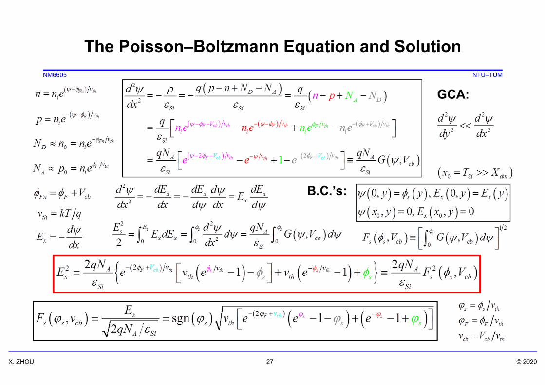
The Poisson–Boltzmann Equation and Solution

NM6605 NTU–TUM
X. ZHOU 28 © 2020
The Complete (“Sah–Pao”) Voltage Equation

NM6605 NTU–TUM
X. ZHOU 29 © 2020
yE y
0nx n cbJ qn dV dx
lnFn th iv n n
n nD kT q
,
ln
ny n y n
n
ni
n Fn
n cb
J x y qn E qD n y
kT nqny qn y
kT nqny q n
qn yqn dV dy
0
, ,
const.
Sitcbds n
s i cb
dVI y W qn x y x y dxdy
W y Q y dV dy
20
1 20 0 0 2
,, ,
, 2
F cb ths s
s F cb th
V vcb A
i cbV v
x cb A Si th
n V qNdx eQ y q n x y dx q n V d q d dd E V qN v e
2
212, sgn 1 1 sgn 2 ,F cb th th thvA
x th A SiV v v
Sith cb
qNE x y ve v e e qN F V
xE x
2
0 0 1 20 22
F cb thdb db s
sb sb F cb th
V vV V
ds i cb ox cbV V V vth
W W eI Q dV C d dVL L v e
2 F cb thV vAn N e
cb Fn FV y y
2
, ,
F cb th
cb di c
V vth
b
v e
F V F V
0 0
, , ,i it t
s ny x y n x y dx n x y dx 0
db db
sb sb
V V
s i cb i cbV Vy Q y dV Q y dV
Drain Current: Pao–Sah Double Integral

NM6605 NTU–TUM
X. ZHOU 30 © 2020
g ox gb FB s oxQ y C V V y Q
i g ox b ox gb FB s sQ y Q y Q Q y C V V y y
i b ox gQ Q Q Q
0
0 0 0
, 1, ,2
ths s
s
vA cb A
b A Ax cb cbA Si
N p Vdx qN eQ y q N p dx q N p d q d dd E V F VqN
0
1 , 02
sAb ox s s
A Si
qNQ y d C yqN
2 22 s F cb thy V y vgb FB s s thV V y y v e
2
2 2
2 2
21
1 1 1 12 2
gb FB scbth
s gb FB s s
oxth ox th ox ox
i b i b
i
i
V V ydV yv
d V V y y
Cv C v C CQ
Q yQy y Q y Q y Q y
cb sds s i
s
iss i s th
drift diff
dV y dI y W y Q yd dy
dQ ydW y Q y W y vdy dy
I y I y
Depletion approximation (n = p = 0; also ND = 0):
Potential/charge balance:
Charge-sheet model (CSM):
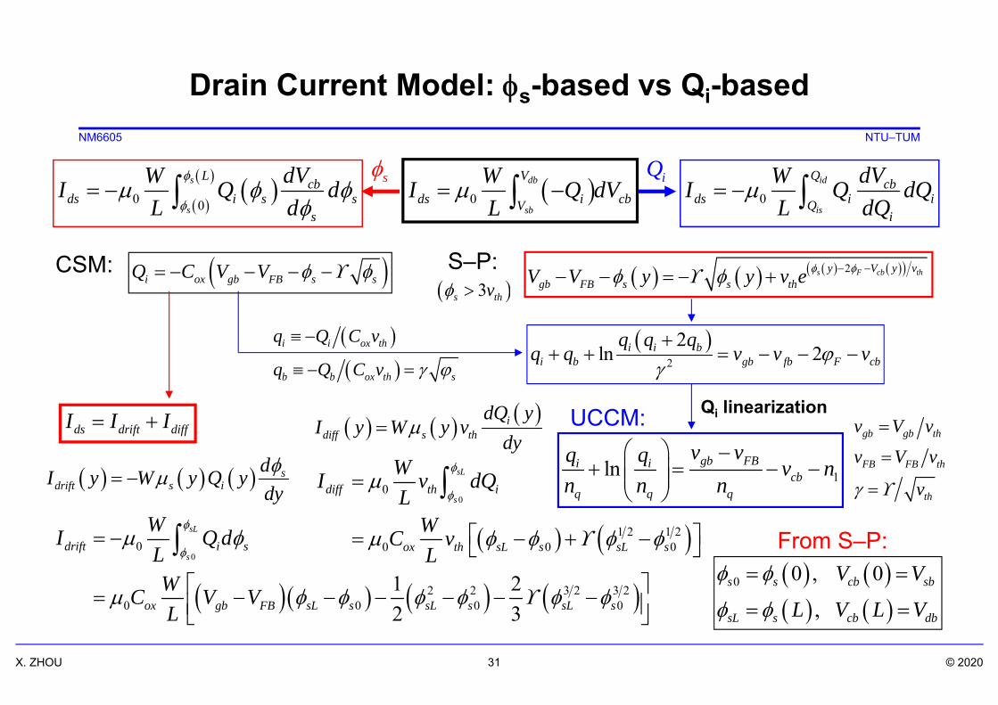
Sah–Pao (‘S–P’) voltage equation (s > 3vth):
CSM
2
122
i s s ox sox ox
bs
dQ d d C dC Cdy dy dy Q dy
CSM: Charge-Sheet Model
NM6605 NTU–TUM
X. ZHOU 31 © 2020
0db
sb
V
ds i cbV
WI Q dVL
0id
is
Q cbds i iQ
i
dVWI Q dQL dQ
0 0
s
s
L cbds i s s
s
dVWI Q dL d
1ln gb FBi icb
q q q
v vq q v nn n n
s
drift s idI y W y Q ydy
idiff s th
dQ yI y W y v
dy
0
0
2 2 3 2 3 20 0 0 0
1 22 3
sL
sdrift i s
ox gb FB sL s sL s sL s
WI Q dLWC V VL
i ox gb FB s sQ C V V
0
0
1 2 1 20 0 0
sL
sdiff th i
ox th sL s sL s
WI v dQL
WC vL
ds drift diffI I I
2s F cb thy V y vgb FB s s thV V y y v e CSM: S–P:
2
2ln 2i i b
i b gb fb F cb
q q qq q v v v
i i ox th
b b ox th s
q Q C v
q Q C v
Qi linearization
3s thv
s iQ
0 0 , 0
,s s cb sb
sL s cb db
V V
L V L V
From S–P:
UCCM:gb gb th
FB FB th
th
v V v
v V v
v
Drain Current Model: s-based vs Qi-based

NM6605 NTU–TUM
X. ZHOU 32 © 2020
0 0db id
sb is
V Q cbds i cb i iV Q
i
dVW WI Q dV Q dQL L dQ
2s F cb th
i ox gb FB s ox s
y V y vox s th ox s
Q C V V C
C v e C
1
cbds s i
s th is i
i
th is i
q ox i
dVI y W Qdy
d v dQW Qdy Q dy
v dQW Qn C Q dy
s q ox s saqn n C
1q b oxn C C 2
oxb
sa
CC
i s
q oxdQ dn Cdy dy
1 thi cb
q ox i
v dQ dVn C Q
lnip i ith p cb
q ox ip
Q Q Qv V Vn C Q
s pip iQ Q
CSM / S–P:
CSM / D+D:
Qi linearization:
UCCM:
ds f rI I I
0
2 2
0 0
1
2
id
is
Q thds i iQ
q ox i
id isth id is
q ox
vWI Q dQL n C Q
Q QW W v Q QL n C L
s is ox th
d id ox th
q Q C v
q Q C v
2 2
2 2ds s d
s ds q q
I q qq qI n n
20,s n th n oxI v C W L
2 22
0 2s d
ds ox th s dq
q qWI C v q qL n
ds drift diffI I I 0
,i sQ y q n x y dx qn y
From UCCM:
Qi-based Current Model

NM6605 NTU–TUM
X. ZHOU 33 © 2020
2
22 2
b ox s ox F sb
ox F sbF sb
Q C C V V y
V yC V
V
2 22 2
i ox gb FB s b
ox gb FB F sb F sbF sb
ox gs t b
Q C V V Q
V yC V V V V y V
V
C V V A V y
Source-referenced threshold condition (“pinned” surface potential):
112 2b
F sb
AV
2 2t FB F F sbV V V
0 00
12
dsV
ds drift i ox gs t b ds dsW WI I Q dV C V V A V VL L
Bulk-charge linearization: Threshold voltage:
Bulk-charge factor:
(For fixed bulk-charge: Ab = 1)
Linear (drift) current: , ,ds s i s i s y y sI y W Q y d dy WQ y v v E E d dy dV dy
(Vgs > Vt)
0 2s F
0 2s s cb F sby V y V V y , 0cb dsV y V y V V
Vt-based Model: Linear (Drift) Current

NM6605 NTU–TUM
X. ZHOU 34 © 2020
b ox ddQ C
s ddy Subthreshold surface potential:
gb FB dd b oxV V Q C
22
2 4dd gb FBV V
2dd F cb thV y vi ox dd th bQ C v e Q
CSM / S–P:
2
2
2
1
12
2
dd F cb th
dd F cb th
dd F cb th
V vthi ox dd ox dd
dd
V vthox dd ox dd
dd
V vthox
dd
vQ C e C
vC e C
vC e
cb sb cb dbis i id iV V V V
Q Q Q Q
0 0id
is
Q
ds th i th id isQ
W WI v dQ v Q QL L
220 1dd F sb th ds thV v V v
ds d thWI C v e eL
22
ox Si A Sid dd
dd dmdd
C q NCX
0 0b
b dd b s dd sdd
QQ Q
00
b s dgb FB dd dd s
ox ox
Q CV VC C
2dd F sb gs tV V V n 0 2s F sbV
' '
0
'2 1gs t th ds th
V V n v V vdds diff ox th
ox
CWI I C v e eL C
Subthreshold (diffusion) current:(Vgs < Vt)
1
12 2
d ox
F sb
n C C
V
'0
' 1.5,t t sff F bo sV V VV
bd
dd
Q C
2 Si dddm
A
XqN
s-based
Vt-based Model: Subthreshold (Diffusion) Current
NM6605 NTU–TUM
X. ZHOU 35 © 2020
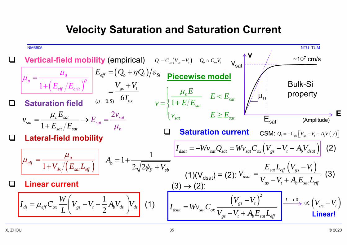
Velocity Saturation and Saturation Current
Vertical-field mobility (empirical)
Saturation field
Lateral-field mobility
Linear current
v
EEsat
vsat
n
Bulk-Siproperty
~107 cm/s
1n
satsat
sat sat
E E EE Ev
v E E
12 san sat
satsat sat
tsat
n
EvE E
vE
Saturation current
12ds eff ox gs t b ds ds
WI C V V A V VL
1n
effds sat effV E L
dsat sat sat sat ox gs t b dsatI Wv Q Wv C V V A V
(1)
(2)
(1)(Vdsat) = (2): sat eff gs t
dsatgs t b sat eff
E L V VV
V V A E L
2gs tdsat sat ox
gs t b sat eff
V VI Wv C
V V A E L
gs tV V 0L
Linear!
112 2b
F sb
AV
0
1n
eff critE E
6
eff b i Si
gs t
ox
E Q Q
V VT
Piecewise model
(3)(3) (2):
i ox gs tQ C V V b ox tQ C V
i ox gs t bQ C V V A V y CSM:
( 0.5)
(Amplitude)

NM6605 NTU–TUM
X. ZHOU 36 © 2020
Charge-Sharing Model: Vt “Roll-Off”
o
n+
LeffTox
Xdm
Vb
VdVs
Vg
Qb
o o
o
n+ NsdXj
0
W
Q'b
Simple “Triangle” Model
Charge shared by the gate/drain
' 2
' '
1
B A eff d d
B A eff d
b dB
b B eff
Q qN W L X X
Q qN W L X
Q XQQ Q L
Charge-sharing model (“triangle”) Without charge-sharing
With charge-sharing2t FB bm ox FV V Q C
' ' 2bmt FB ox FV V Q C
'' 1
222
bm bm bm
bm
dmt t t
ox ox eff
F sb oxA dm dm Si
ox ox eff o jx g
Q Q Q XV V VC Q C L
V TX
qN X XT L L
2eff g jL L X
Lg
2 2dm Si F sb AX V qN
ox ox oxC T bm A dmQ qN X
Lg
Vt
Short-channel effect (SCE):Vt “roll-off”
Vt
Total bulkcharge:
Bulk chargeper unit area:
(Leff)
0dsV

NM6605 NTU–TUM
X. ZHOU 37 © 2020
Charge-Sharing Model: Vt “DIBL”
Charge-sharing model (“trapezoidal”) Source-end (linear): (Vds = Vd0)
Drain-end (saturation): (Vds = Vdd)
Average depletion width: (any Vds)
DIBL: Drain-Induced Barrier Lowering
, 2 2dm s Si F sb AX V qN
o
n+
LeffTox
Xdm,s
Vb
VdVs
Vg
Qb
o o
o
n+ NsdXj
0
W
Q'b
Charge shared by the drain
Lg y
Lg
Vt
Vt0
Vts
Vt0
, ,
22 22
2
dm s dm ddm
F sb F ds d bSi
A
X XX
V V
qN
Xdm,d
, 2 2dm d Si F db AX V qN
db sb dsV V V
0DIBL g t g ts gV L V L V L
00
ds dt t t V V
V V V
2 2t FB F F sbV V V
222 2
,2 2
F sb F dbdm Si oxAt s
s d
db ds
ox ox e f jf ox g
V VX TqNV VL X
VT L
ds ddts t t V V
V V V
Vts
'b A dm effQ qN X L
Trapezoidalarea = “box”
VDIBL
“Dynamic depletion” (DD)
/0 0.~ .76 / 0d

NM6605 NTU–TUM
X. ZHOU 38 © 2020
Reverse Short-Channel Effect: Vt “Roll-Up” & “Halo”
Lg
Vt
Vt0
Reverse SCE: “Halo”
y
Neff
“Halo” o
n+
LeffTox
Xdm,s
Vb
VdVs
Vg
Qb
o o
o
n+ NsdXj
0
W
Q'b
Lg y
Xdm,d
Empirical RSCE model (“halo”)
Halo pile-up: ()
Halo lateral spread: ()
Replacing all previous NA by Neff
cosh 2pile
efe
Afff
NN
L lN
pile AN N
0.252 F sbl V ln iAF kT q N n
2y
pil
pl
leN y eN
0
effL
p effeff
eff eA
pile
ff
N y dy LN eN
l l ll l
rf erfL L
N
Gaussian halo model
Halo dose, tilt, energy
NA

NM6605 NTU–TUM
X. ZHOU 39 © 2020
Summary of Important (Simple) Equations
Effective body doping and related equations Halo doping
Threshold voltage Long-channel (1D theoretical model)
Any channel-length and body/drain-bias
2 Si eff
ox
NqC
ln efF h
i
ft n
Nv
2M sFB MS ox ox F oxg sNV E qQ C C
ox o oxxC T
1 d oxn C C d Si dmC X cosh 2pile
efe
Afff
NN
L lN
pile AN N 0.252 sbFl V
lnth iAF v nN Physical quantities 2geff jdL XL
oox x o SSi i o
2 2Si F sdm
eff
bVX
Nq
000
dssb
dt t t V VV
V V V
22 2
ss bFst gs F F bV FBV V V V
0dssb
ddts t t V VV
V V V
2, , 2 22 2
Sit t t t eff F F
oxs
oxsb ox sb sb
g dds sd
jd
TV T V VL X
V V V V N VV
Linear Vt0:
Saturation Vts:
0.0259thv
VqTk
, , , , ,g ox j M ssL T X N TPhysical parameters:
(Physical constants)
NM6605 NTU–TUM
X. ZHOU 40 © 2020
Summary of Important (Simple) Equations
Drain current Bulk-charge factor
Linear
Saturation
Subthreshold
1, ,2dlin eff ox t b
esgs gsds ds ds
ffb
WVI C V AVV VV VL
2, , ds
tdsat ox
t b ss
at e
gsgs
ffsb t
gsa
V VI C
V A EV WVV
Vv
L
2, , 1gs t dsth thV nv v
dsub n d theff
Vds
Vsbgs
WVI C v e eVVL
Drive current Ion:
2 asat
n
s tvE
1 ds
neff
sat effV E L
112 2b
F sbVA
0
1n
eff critEE
6gs
fox
tef
VVE
T
Mobility Vertical-field
0, ,on dsat ddd dVI VI
, ,00off dsub ddI I V
Leakage current Ioff:
/
0
, , , ,, , , ,
A d s d
sat crit
Nv E
Fitting parameters:(TCAD: W = 1 m)
Lateral-field
00
0
, ,
, ,dlin
dl
g ds
sin ddd
V
I
V
VV
I
, ,
, ,
0
0dsat
ds
gs dd
dat sdd
VI
I
V
VV
0 0, ,
, ,
0
0
dsub
ds
gs
ubs
d
ddgs
I
I
V V
VV