design and implementation of a current controlled grid
TRANSCRIPT

Design and implementation of a current controlled grid connectedinverter for thermoelectric generator sources
B BIJUKUMAR, G SARAVANA ILANGO* and C NAGAMANI
Department of Electrical and Electronics Engineering, National Institute of Technology, Tiruchirappalli 620015,
India
e-mail: [email protected]; [email protected]; [email protected]
MS received 8 May 2019; revised 23 January 2020; accepted 3 February 2020
Abstract. This paper presents the digital implementation of a current controlled grid connected inverter for
Thermoelectric Generator (TEG) sources. Considering the electrical characteristics of a TEG source, several
important aspects that a designer has to consider in selecting the rating of power converters for the grid
connected operation of TEG source are discussed. The closed loop control of a TEG fed grid connected voltage
source inverter (VSI) requires line current control to regulate the power pumped into the grid. Considering the
inverter, current sensor and line inductor models, a simplified method is espoused to determine the parameters of
the digital current controller. An Altera Cyclone II FPGA board is used to implement the current control strategy
in VSI fed with TEG power source. The proposed design approach is validated using simulations and experi-
ments and verified with the time domain specifications.
Keywords. Current control; grid connected system; thermoelectric generator (TEG); vector control; voltage
source inverter (VSI).
1. Introduction
As the demand for energy is escalating, renewable energy
sources such as photovoltaic (PV), wind energy systems,
thermoelectric generators (TEG), etc. need to be harvested
in a significant measure. TEGs are popular among the non-
conventional energy sources because of the global warming
and energy crisis problems. TEG is a potential source
which provides an effective way to generate electric power
from waste heat. Many research works reported the
potential application of TEG source in automobiles, electric
hybrid vehicle, combustion systems, etc. [1–3].
The electrical P–V characteristics of a TEG module are
parabolic whereas the I–V characteristics are linear in nat-
ure and a unique Maximum Power Point (MPP) exists. The
output power of a thermoelectric generator depends on the
temperature difference across the junctions of the device.
Several studies reported on the implementation of Maxi-
mum Power Point Tracking (MPPT) algorithms to extract
maximum power from the device [4–7]. A temperature
mismatch study was carried out in series and parallel TEG
array configurations and the power loss due to temperature
mismatch was experimentally quantified [8]. A differential
power processing architecture was developed to increase
the output power of the TEG source under temperature
mismatched conditions [9]. However, the grid connected
TEG systems is not adequately reported in literature.
This paper presents the design and development of a
current controlled VSI for TEG sources based on d–q
control theory. Vector control based on d–q control theory
is a popular method used to implement the closed loop
current control system for a grid connected inverter system,
front end converter, etc. [10–14]. The vital role of the
power converter is to inject the current with a low Total
Harmonic Distortion (THD). The single-phase steady state
equivalent circuit of a grid connected system is shown in
figure 1, where RS and LS are the resistance per phase and
inductance per phase of the inductor, respectively and d is
the transmission angle.
The real and reactive power flows between inverter and
grid are given as follows,
P ¼ VE
Zcos h� dð Þ � V2
Zcos h ð1Þ
Q ¼ VE
Zsin h� dð Þ � V2
Zsin h ð2Þ
where, Z is the line impedance and h is the impedance
phase angle.
From eequations (1) and (2), it is clear that the active and
reactive power flow depend on the magnitude and phase of
the inverter voltage with respect to utility grid. Thus, by
varying the phase angle and magnitude of the VSI, the*For correspondence
Sådhanå (2020) 45:121 � Indian Academy of Sciences
https://doi.org/10.1007/s12046-020-01328-ySadhana(0123456789().,-volV)FT3](0123456789().,-volV)

phase angle and magnitude of the line current can be
controlled indirectly.
This work focuses on the digital implementation of
current controlled VSI for TEG systems. In particular,
design procedure is proposed for implementing the vector
control in a grid connected voltage source inverter (VSI)
fed from a TEG source. Several important parameters need
to be considered for implementing the vector control in a
digital current controller. The experimental characteristics
of a TEG source and the requirements of power converters
for a grid connected TEG application are discussed in
section 2. The steps involved in designing the current
controller are illustrated in section 3. The simulation and
test results are given in section 4.
2. TEG system
This section deals with the study on the selection of power
converters for the grid interfacing of a TEG source. Tra-
ditionally, the commercially available TEG modules are
fabricated as low output voltage devices [15]. Hence, it is
necessary to boost the output voltage of the TEG array to
obtain the appropriate dc link voltage for interfacing with
the grid through a VSI.
2.1 Equivalent circuit of a TEG
Under steady state, the electric circuit of a TEG source can
be modelled as shown in figure 2 [16].
Applying Kirchhoff’s Voltage Law, the voltage across
the TEG terminals can be expressed as follows,
VTEG ¼ VOC � ITEG � Rint ð3Þwhere VOC and Rint are the open-circuit voltage and internal
resistance of a TEG, respectively.
The voltage generated across the module is given by,
VOC ¼ a� Th � Tcð Þ ¼ a� DT ð4Þwhere a is the Seebeck coefficient, Th is the hot side tem-
perature and Tc is the cold side temperature of the device
and DT is the temperature gradient. From (3) it is clear that,
the I–V characteristics of a TEG source are linear in nature.
The power produced by the TEG source can be expressed
as,
PTEG ¼ VOC
Rint
� VTEG � 1
Rint
� �� V2
TEG ð5Þ
Equation (5) is in the form of a parabolic equation. The
condition for maximum power can be derived as follows,
VTEG;max ¼ VOC
2ð6Þ
ITEG;max ¼ ISC
2ð7Þ
where VOC is the open-circuit voltage and ISC is the short-
circuit current of the device.
Hence, the maximum power obtained from the TEG
(PTEG,max) is 25% of the product of the VOC and ISC.
2.2 Experimental characterization of a TEG
source
In order to demonstrate the electrical characteristics of a
TEG source, a test set-up has been developed in the labo-
ratory. The schematic diagram and snapshot of the exper-
imental set-up are shown in figures 3 and 4, respectively.
The experimental set-up comprises of temperature mea-
suring and control units to control the temperature gradient
across the junctions of TEG module. The TEG-12708T237
module is considered for the study [17]. The heat is sup-
plied from electric heaters, which are controlled using
temperature controllers and relays. The TEG module is
sandwiched between heat spreader plate and Aluminium
heat sink. The cold side of the devices are cooled using
fans. In order to measure the hot and cold side temperatures
of the device, thermocouples are embedded into heat
spreader plate and heat sink. An Agilent data logger unit is
used to log the temperature gradient across the modules.
The electrical characteristics of the device are obtained by
sweeping the loading rheostat, for different temperature
gradients across the module. The electrical characteristics
of the TEG module are plotted for a temperature gradient of
Figure 1. Steady state equivalent circuit of a grid connected
inverter system.
Figure 2. Equivalent circuit of the TEG source.
121 Page 2 of 13 Sådhanå (2020) 45:121

80�C, 65�C and 45�C. The corresponding I–V and P–V
characteristics of the tested module are shown in figures 5
and 6, respectively.
From figures 5 and 6, it can be seen that the I–V and P–V
curves of a TEG module are linear and parabolic in nature
Figure 3. Schematic diagram of the experimental set-up.
Figure 4. Snapshot of the experimental set-up (a) System
arrangement. (b) Arrangement of TEG modules.
Figure 5. I–V characteristics of a TEG module (experimental).
Figure 6. I–V characteristics of a TEG module (experimental).
Sådhanå (2020) 45:121 Page 3 of 13 121

for different values of temperature gradient. It can also be
noted that the MPP of a TEG source occur at 50% of the
open-circuit voltage and 50% of the short-circuit current.
2.3 Selection of rating of boost converter
Consider a TEG array which feeds a dc–dc converter whose
P–V and I–V characteristics are shown in figure 7. In this
scenario, the TEG designer has to select a boost converter
with a rated voltage of Vrated and a current rating of Irated set
to be greater than or equal to VOC and ISC of the TEG array
respectively, by considering the Safe Operating Area
(SOA) of the power electronic switches in the converter.
Hence, the minimum power rating of the dc-dc converter is
given as,
Pboost ¼ VOC � ISC ¼ 4� PTEG;max ð8ÞFrom equation (8), it is clear that, in order to feed a boost
converter from a TEG array, its power rating must be equal
to four times that of TEG array. Now, considering a boost
converter whose rated current is 1.25 times IMPP of the
TEG array. Therefore, the power rating of the boost con-
verter with Vrated set to be VOC of the TEG array and Iratedas 125% of IMPP of the array, can be given as follows,
Pboost;new ¼ VOC � 1:25� IMPP ¼ 2:5� PTEG;max ð9ÞFrom equations (8) and (9), it is clear that the power rating
of the boost converter can be effectively reduced by
selecting the rated current equal to 125% of IMPP of the
TEG array. However, since the operating current of the
TEG array exceeds the rated current of the boost converter,
a current limiter is necessary to confirm the safe operation
of the converter. Hence, by adding a current limiter in the
vector controlled VSI, the operating current of the con-
verter can be confined to be within the rated value, Ilimit as
given in figure 7.
The block schematic of the current controlled gird con-
nected TEG system is shown in figure 8, where the MPPT
control is implemented in the dc-dc boost converter and
current control is employed in the VSI.
3. Design of current controller
This section illustrates a design procedure for selecting the
parameters of the d and q-axes current controllers. In the
context of digital implementation of current controller in
grid connected TEG applications, the computation of
desired controller parameters plays a vital role to accom-
plish a good transient response. Hence, it is necessary to
develop the appropriate models of the sub-blocks in the
closed loop current controller and are given as:
1. The current sensors used for measuring the grid currents.
2. The VSI tied to the grid line.
Figure 7. Electrical characteristics of a TEG source.
Figure 8. Schematic diagram of current controlled grid connected TEG system.
121 Page 4 of 13 Sådhanå (2020) 45:121
3. The line inductance between the inverter and grid
terminals and,
4. PI controllers for q and d axes current control.
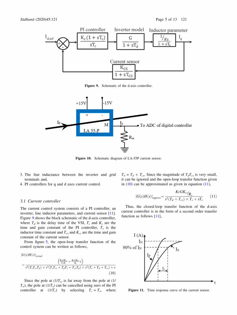
3.1 Current controller
The current control system consists of a PI controller, an
inverter, line inductor parameters, and current sensor [11].
Figure 9 shows the block schematic of the d-axis controller,
where Td is the delay time of the VSI, Tc and Kc are the
time and gain constant of the PI controller, Ts is the
inductor time constant and Tcs and Kcs are the time and gain
constant of the current sensor.
From figure 5, the open-loop transfer function of the
control system can be written as follows,
GðsÞHðsÞj jactual
¼KcGKcs
TcRsþ KcGKcs
Rss
� �s4 TsTcsTdð Þ þ s3 TsTcs þ TdTs þ TcsTdð Þ þ s2 Ts þ Td þ Tcsð Þ þ s
ð10ÞSince the pole at (1/Ts) is far away from the pole at (1/
Tr), the pole at (1/Ts) can be cancelled using zero of the PI
controller at (1/Tc) by selecting Tc = Ts, where
Tr = Td ? Tcs. Since the magnitude of TdTcs is very small,
it can be ignored and the open-loop transfer function given
in (10) can be approximated as given in equation (11),
GðsÞHðsÞj japprox¼KcGKcs=Rs
s2 Td þ Tcsð Þ � Ts þ sTsð11Þ
Thus, the closed-loop transfer function of the d-axis
current controller is in the form of a second order transfer
function as follows [11],
Figure 9. Schematic of the d-axis controller.
Figure 10. Schematic diagram of LA-55P current sensor.
Figure 11. Time response curve of the current sensor.
Sådhanå (2020) 45:121 Page 5 of 13 121

IdðsÞId;ref ðsÞ ¼
KcG
RTsTr
1þ sTcsð Þs2 þ s
Trþ KcGKcs
RTsTr
� � ð12Þ
From equation (12), the damping ratio can be written as
follows,
e ¼ 1
2Trxn
ð13Þ
where xn ¼ffiffiffiffiffiffiffiffiffiffiffiKcGKcs
RsTsTr
qis the natural frequency of oscillation.
3.1a Design of inverter The VSI can be modelled by its
time constant Td and gain constant G as shown in figure 9
[12]. The time delay of the inverter is given by,
Td ¼ 1
2fcð14Þ
where fc is the frequency of the carrier signal.
The inductor time constant is given by,
Ts ¼ Ls
Rs
ð15Þ
3.2a Design of current sensor The current sensor can be
modelled by means of time and gain constant as shown in
figure 9. The first order transfer function of the current
sensor is given as follows,
GCSðsÞ ¼ KCS
1þ sTCSð16Þ
where KCS and TCS are the gain and time constant of the
current sensor, respectively.
The schematic diagram of a LA 55-P current transducer
is shown in figure 10 [18], where IP and IS are the primary
and secondary rms currents, and Rm is the measuring
resistance.
The gain constant of the current sensor can be deter-
mined as follows,
KCS ¼ IP � KN � Rm ð17Þwhere KN is the conversion ratio of the LA 55-P current
sensor.
Figure 12. Design of PI controller (a) Block diagram. (b) Limit
settings of saturation block.
Figure 13. Digital implementation of PI controller.
121 Page 6 of 13 Sådhanå (2020) 45:121

The transient response characteristics of LA 55-P current
sensor is shown in figure 11, where tr -is the response time
of the sensor. The response time of LA 55-P current sensor
is less than 1 ls.
The time constant of the current sensor can be calculated
as follows,
TCS ffi 10� tr ð18Þ3.2c Design of PI controller: From the transfer function of
the current controller given by (12) the controller parame-
ters can be determined as follows: The proportional gain
constant of the P controller is given by,
KC ¼ RS � TS
4e2GKCSTrð19Þ
Also, the integral gain constant of the I controller is
given by,
Table 1. Specifications of TEG module
Sl. nos. Parameters Symbol Value
1. TEG power PMPP 21.6 W
2. Open-circuit voltage VOC 14.4 V
3. Short-circuit current ISC 6.0 A
4. Voltage at MPP VMPP 7.2 V
5. Current at MPP IMPP 3.0 A
6. Seebeck coefficient a 0.0533 V/K
7. Internal resistance Rint 2.39 X
Figure 14. Grid connected TEG system (a) Schematic diagram. (b) Control block diagram.
Sådhanå (2020) 45:121 Page 7 of 13 121

Ki ¼ Kp
TC¼ RS � TS
4e2GKCSTrTCð20Þ
The figure 12a and b show the block diagram and the
limit settings of saturation block of the PI controller, where
KC and Ki are the proportional and integral constants,
respectively. In case of digital implementation of the con-
troller, a saturation block should be added to the integrator
output, in order to maintain the system in safe operating
region. The saturation limits should be selected as equal to
the per unit value of the magnitude of the carrier signal as
shown in figure 12b.
i:e; þVc;pu � Limit� � Vc;pu ð21Þwhere Vc,p.u is the magnitude of the triangular wave used
for digital implementation.
If the limits are set to be less than ?Vc,pu and -Vc,p.u,
then the controller may not follow the reference signal
since the output response gets limited corresponding to the
settings. The processing time of the PI controller can be
selected as tpi ffi 10� Td . Similarly, the closed loop q-axis
controller can also be designed.
The normalized equation of the d-axis current controller
can be written as,
Vud ¼ 1
Tc
ZVid;ref � Vid
� �� Kc � dt þ Vid;ref � Vid
� �� Kc
ð22Þwhere Vud, Vid,ref and Vid -are the normalized in the FPGA
board values of Ud, Id,ref and Id respectively.
By using Euler’s method of integration,
VudðnÞ ¼ DtTc
� Kc � Vid;errorðnÞ þ Iðn� 1Þþ Vid;errorðnÞ � Kc
ð23Þ
where Vid,error = Vid,ref - Vid and I(n - 1) is the previ-
ous value of the output of the Integral-controller.
According to (23), a PI-controller can be digitally
implemented as shown in figure 13. The processing time
of the PI-controller can be selected as tpi ffi 10� Td.
Similarly, the closed loop q-axis controller can also be
designed.
4. Simulations and experimentation
This section presents the details of implementation of the
current controller in Matlab/Simulink and in the FPGA
platform. Further, the results are illustrated.
Figure 15. Bode plots of |G(s)H(s)|actual and |G(s)H(s)|approx transfer functions of current loop.
Table 2. System and controller parameters
Sl. nos. Parameters Symbol Value
1. DC link voltage Vdc 60 V
2. Inductance of the line inductor Ls 10 mH
3. Resistance of the line inductor Rs 0.5 X4. Time constant of line inductor Ts 20 ms
5. Frequency of the carrier signal fc 5 kHz
6. Peak voltage of the carrier signal Vc 5 V
7. Gain of the inverter G 6
8. Delay time of the inverter Td 100 ls9. Gain of the current sensor Kcs 0.22
10. Time constant of the current sensor Tcs 10 ls11. Proportional gain of the controller Kc 34.44
12. Integral gain of the controller Ki 1722
121 Page 8 of 13 Sådhanå (2020) 45:121
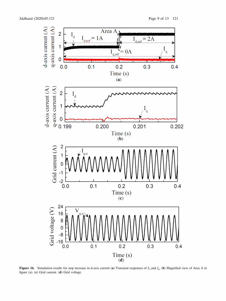
Figure 16. Simulation results for step increase in d-axis current (a) Transient responses of Id and Iq. (b) Magnified view of Area A in
figure (a). (c) Grid current. (d) Grid voltage.
Sådhanå (2020) 45:121 Page 9 of 13 121

4.1 System description
A current controlled VSI is modelled and simulated in the
MATLAB/Simulink environment. An Agilent E4360 pro-
grammable dc power supply is used to power the VSI
which emulates the characteristics of a TEG. A series
connected TEG array comprising of eleven TEG-
12708T237 modules is considered for the study. The
parameters of the TEG module are shown in table 1 [17]. A
three-phase IGBT based PWM inverter (Semikron) module
available in the laboratory is tied to the three-phase grid
through a step-up transformer. The grid voltages and cur-
rents are measured using LEM voltage sensor LV 25-P and
LEM current sensor LA 55-P, respectively. The control
algorithms are implemented in an Altera Cyclone II FPGA
digital controller. The schematic diagram and control block
diagram of the test set-up are shown in figure 14a and b,
respectively.
4.2 Design of current controller
The design of a current controller is explained in the
following:
• For the selected TEG array, the VOC of the array is 120
V at Th = 230�C and Tc = 25�C. Since the voltage of
the TEG array at MPP is 50% of the VOC, Vdc can be
selected as 60 V. For the digital implementation of
SPWM pulses, the Vc and fc of the triangular wave are
selected as 5 V and 5 kHz, respectively. Based on the
selected values, the G and Td of the inverter can be
calculated using (14). In this design, G = 6 and
Td = 100 ls. The time constant of the inductor is
calculated as 20 ms using (15).
• For the LA 55-P current sensor used to sense the grid
currents, the design parameters are IP = 1 A, KN = 1/
1000 and Rm = 220 X. The gain of the current sensor iscalculated as 0.22 using (17). The tr of the LA 55-P
sensor is 1ls and TCS is selected as 10 ls.• The gain constants of the PI controller are computed to
be 34.44 and 1722 respectively. The damping ratio e ischosen as 0.707. Since Vc is 5 V, the limit settings of the
saturation block are selected to be equal to the equivalent
per unit value of Vc in FPGA digital controller.
• In order to validate the approximation in open loop
transfer function (11), the bode plots of the actual (10)
and approximated open loop transfer functions (11) are
plotted as shown in figure 15. From figure 15, the xc is
obtained as 4140 rad/s and the phase margin (PM) is 65�.The gain margin (GM) of the system is observed to be 28
dB. It can be seen that, the pole cancellation in the actual
open-loop transfer function (10) does not affect the
stability of the system. Hence, the settling time of the
system can be estimated as 0.966 ms considering ts = 4/
xc [19]. The control parameters used for simulations and
experiments are given in table 2.
4.3 Simulations and test results
In order to test the performance of the current controller, a
series connected TEG array is considered and the temper-
ature gradient of the TEG module is set at 205�C
Figure 17. System response to a step increase in Id (experimental).
121 Page 10 of 13 Sådhanå (2020) 45:121

Figure 18. Simulation results for step change in q-axis current (a) Transient responses of Id and Iq. (b) Magnified view of Area B in
figure (a). (c) Grid current. (d) Grid voltage.
Sådhanå (2020) 45:121 Page 11 of 13 121
(Th = 230�C and Tc = 25�C). To interpret the performance
of the d-axis current controller, a step change in d-axis
reference current (Id,ref) from 1 A to 2 A is introduced at
t = 0.2 s. While the q-axis reference current (Iq,ref) is set at
0 A. Figure 16 shows the dynamic response (simulations)
of d-axis current, grid voltage and grid current. The settling
time of the system is 0.6 ms (figure 16b) which is close to
that obtained from frequency response plots (0.966 ms).
Also, the current is injected into the grid at a unity power
factor as shown in figure 16c and d.
The experimental results are depicted in figure 17, where
the settling time is observed to be 2.2 ms which is close to
the designed value.
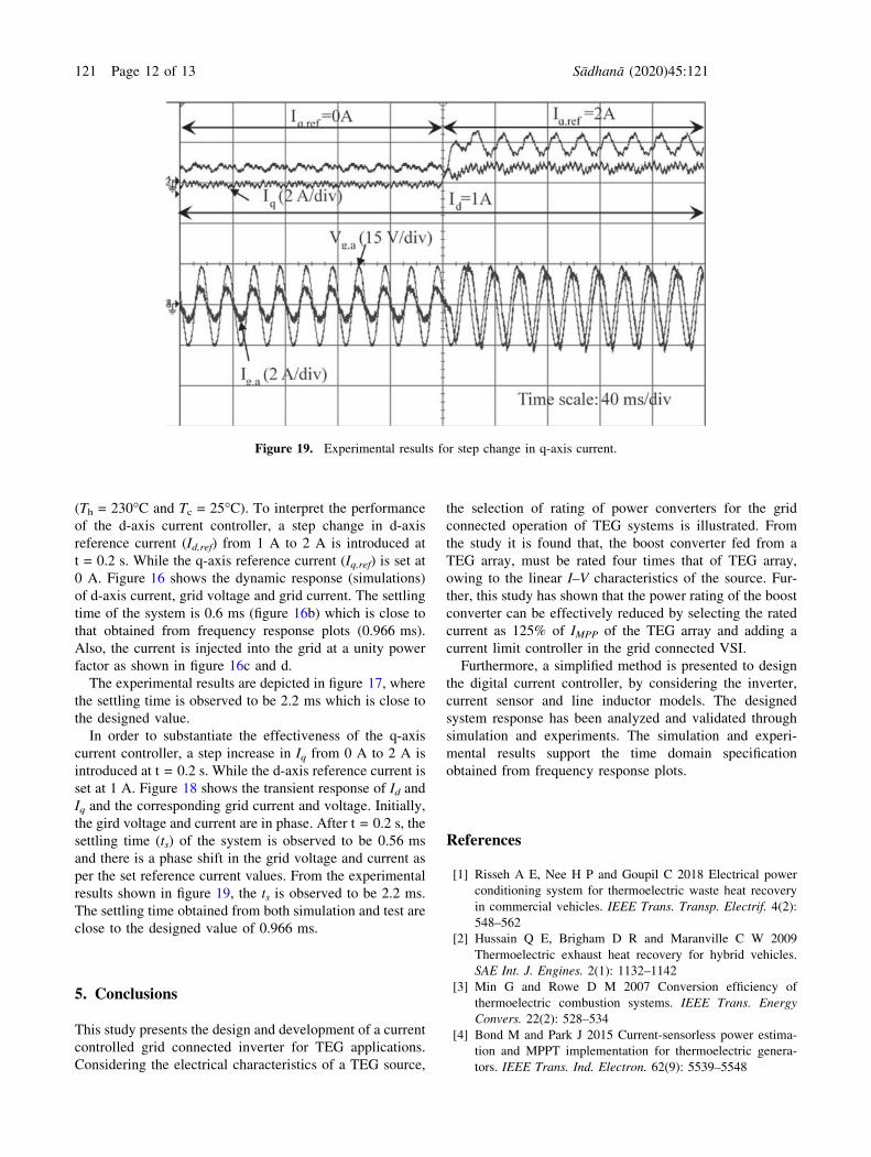
In order to substantiate the effectiveness of the q-axis
current controller, a step increase in Iq from 0 A to 2 A is
introduced at t = 0.2 s. While the d-axis reference current is
set at 1 A. Figure 18 shows the transient response of Id and
Iq and the corresponding grid current and voltage. Initially,
the gird voltage and current are in phase. After t = 0.2 s, the
settling time (ts) of the system is observed to be 0.56 ms
and there is a phase shift in the grid voltage and current as
per the set reference current values. From the experimental
results shown in figure 19, the ts is observed to be 2.2 ms.
The settling time obtained from both simulation and test are
close to the designed value of 0.966 ms.
5. Conclusions
This study presents the design and development of a current
controlled grid connected inverter for TEG applications.
Considering the electrical characteristics of a TEG source,
the selection of rating of power converters for the grid
connected operation of TEG systems is illustrated. From
the study it is found that, the boost converter fed from a
TEG array, must be rated four times that of TEG array,
owing to the linear I–V characteristics of the source. Fur-
ther, this study has shown that the power rating of the boost
converter can be effectively reduced by selecting the rated
current as 125% of IMPP of the TEG array and adding a
current limit controller in the grid connected VSI.
Furthermore, a simplified method is presented to design
the digital current controller, by considering the inverter,
current sensor and line inductor models. The designed
system response has been analyzed and validated through
simulation and experiments. The simulation and experi-
mental results support the time domain specification
obtained from frequency response plots.
References
[1] Risseh A E, Nee H P and Goupil C 2018 Electrical power
conditioning system for thermoelectric waste heat recovery
in commercial vehicles. IEEE Trans. Transp. Electrif. 4(2):
548–562
[2] Hussain Q E, Brigham D R and Maranville C W 2009
Thermoelectric exhaust heat recovery for hybrid vehicles.
SAE Int. J. Engines. 2(1): 1132–1142
[3] Min G and Rowe D M 2007 Conversion efficiency of
thermoelectric combustion systems. IEEE Trans. Energy
Convers. 22(2): 528–534
[4] Bond M and Park J 2015 Current-sensorless power estima-
tion and MPPT implementation for thermoelectric genera-
tors. IEEE Trans. Ind. Electron. 62(9): 5539–5548
Figure 19. Experimental results for step change in q-axis current.
121 Page 12 of 13 Sådhanå (2020) 45:121

[5] Montecucco A and Knox A R 2015 Maximum power point
tracking converter based on the open-circuit voltage method
for thermoelectric generators. IEEE Trans. Power Electron.
30(2): 828–839
[6] Carreon-Bautista S, Eladawy A, Mohieldin A N and
Sanchez-Sinencio E 2014 Boost converter with dynamic
input impedance matching for energy harvesting with multi-
array thermoelectric generators. IEEE Trans. Ind. Electron.
61(10): 5345–5353
[7] Kim J and Kim C 2013 DC–DC boost converter with
variation-tolerant MPPT technique and efficient ZCS circuit
for thermoelectric energy harvesting applications. IEEE
Trans. Power Electron. 28(8): 3827–3833
[8] Montecucco A, Siviter J and Knox A R 2014 The effect of
temperature mismatch on thermoelectric generators electrically
connected in series and parallel. Appl. Energy 123: 47–54
[9] Sun K, Qiu Z, Wu H and Xing Y 2018 Evaluation on high-
efficiency thermoelectric generation systems based on
differential power processing. IEEE Trans. Ind. Electron.
65(1): 699–708
[10] Choi J and Sul S 1998 Fast current controller in three-phase
AC/DC boost converter using d-q axis. IEEE Trans. Power
Electron. 13(1): 179–183
[11] Prasad J S, Bhavsar T, Ghosh R and Narayanan G 2008
Vector control of three-phase AC/DC front-end converter.
Sadhana 33(5): 591–613
[12] Krishnan R 2001 Electric motor drives: modeling, analysis
and control. Prentice Hall
[13] Sato Y, Ishizuka T and Nezu T 1998 A new control strategy
for voltage-type PWM rectifiers to realize zero steady-state
control error in input current. IEEE Trans. Ind. Appl. 34(3):
480–486
[14] Lee T and Liu J 2011 Modeling and control of a three-phase
four-switch PWM voltage-source rectifier in d–q syn-
chronous frame. IEEE Trans. Power Electron. 26(9):
2476–2489
[15] Cao D and Peng F Z 2011 Multiphase multilevel modular
dc–dc converter for high-current high-gain TEG application.
IEEE Trans. Ind. Appl. 47(3): 1400–1408
[16] Lineykin S and Ben-Yaakov S 2007 Modeling and analysis
of thermoelectric modules. IEEE Trans. Ind. Appl. 43(2):
505–512
[17] Data sheet of Thermoelectric Generator TEG-12708T237
[18] Data sheet of LEM sensor LA-55P
[19] Engelberg S 2005 A mathematical introduction to control
theory. Imperial College Press
Sådhanå (2020) 45:121 Page 13 of 13 121