design and implementation of a 16-bit, low-power, high
TRANSCRIPT

THE DESIGN AND IMPLEMENTATION OF A 16-BIT,LOW-POWER, HIGH PERFORMANCE, MICROPROCESSOR BASED
DIGITAL SIGNAL PROCESSING UNIT/
by
Michael D. Gaches
B. S., Kansas State University, 1984
MASTER'S THESIS
submitted in partial fulfillment of the
requirements for the degree
MASTER OF SCIENCE
Department of Electrical and Computer Engineering
KANSAS STATE UNIVERSITYManhattan, Kansas
1987
Approved by:
Major Professor

A11ED7 3Dbfl3D
TABLE OF CONTENTS
Page1.0 Introduction 1
X2.0 Processor Description 4
2 .
1
Chip Description 42.2 Processor Architecture 5
2.2.1 Executive Entry Table 52.2.2 Memory Addressing 62.2.3 Executive and User Process State
Tables 72.2.4 Executive and User Stacks 92.2.5 Task Scheduling and Context Switching 13
2.3 External Processor Interrupts 15
2.3.1 Processor Reset 152.3.2 Bus Error Interrupts 162.3.3 Nonmaskable and Maskable Interrupts 17
2.4 Exceptions 182.5 Processor Data Types and Addressing
Information 19
2.5.1 Boolean Data 192.5.2 Character Data 192.5.3 Integer Data 192.5.4 Fractional Data 202.5.5 Floating Point Data 20
2.6 Addressing Modes 212.7 Bus Interface 212.8 Bus Timing 25
3.0 System Description 28
3.1 Design Considerations and Constraints 293.2 Hardware Description 30
3.2.1 Clock, Reset and Set-up Select 313.2.2 Synchronous-vs-Asynchronous Bus
Protocol 363.2.3 System Decoding 383.2.4 ROM System Interface 403.2.5 RAM System Interface 42
3.3 8-bit Port and Test I/O 443.4 Alarm Outputs 453.5 ADC Interface 45
ii

Page3.6 System Software Description 47
4.0 System Performance 49
4.1 System Power Consumption 49
4.2 System Throughput 504.3 System Compatibility 51
5.0 Concluding Remarks 52
Acknowledgements 53
References 54
Appendices
Appendix A: CMOS-vs-SOS/CMOS Versions of the AdvancedArchitecture Microprocessor (AAMP) 55
Appendix B: Parts List and Board Layout 59
Appendix C: "Stripped Down" AAMP Signal ProcessingUnit 62
Appendix D: Widrow Adaptive Linear PredictorAlgorithm Listing 67
iii

LIST OF FIGURES
PageFigure 1. Memory Addressing Format 7
Figure 2. Executive and User PSD Tables 8
Figure 3. Process Stack 11
Figure 4. Procedure Call Operation 12
Figure 5. Procedure Return Operation 13
Figure 6. AAMP Bus Timing 23
Figure 7. CMOS and TTL, Speed-vs-Power 31
Figure 8. System Block Diagram 32
Figure 9. System Schematic 33
Figure 10. External Oscillator 34
Figure 11. Transfer Acknowledge (XAK) Generation 37
Figure 12. EPROM Bus Timing 41
Figure 13. RAM Bus Timing 43
Figure Bl. AAMP Signal Processing Unit Board Layout 61
Figure CI. "Stripped Down" AAMP Signal Processing Unit 64
iv

LIST OF TABLES
PageTable l. Executive Entry Table 6
Table 2. Data Transfer Timing Parameters 24
Table 3. Memory Speed-vs-Set-up Select 35
Table 4. Read/Write Bus Cycle Time-vs-Set-up Select 37
Table 5. System Memory Map 39
Table 6. System Executive Entry Table 48
Table 7. System Power Consumption 49
Table 8. System Throughput 51
Table Al. Pin-out Changes to the AAMP 56
Table CI. "Stripped Down" AAMP System Memory Map 65
1. Introduction
The purpose of this thesis is to present the design and
implementation of a low-power, high-performance,
microcomputer-based system for signal processing
applications. The processor chosen for this project is
Rockwell International's Advanced Architecture Microprocessor
or simply AAMP. This research is sponsored by Sandia
National Laboratories and is part of an ongoing evaluation of
the AAMP by the Department of Electrical and Computer
Engineering at Kansas State University. Previous research
conducted at Kansas State University on the AAMP includes a1
software and instruction set evaluation by Kenneth Albin and2
an overall hardware evaluation by Gary Mauersberger . This
thesis is not meant to duplicate the research accomplished by
Mr. Albin and Mr. Mauersberger but is meant to build on their
work by incorporating the AAMP into a specific system design.
This design utilizes the AAMP as a central processing unit
for an ADC based intruder detection system. The system which
is currently being used by Sandia is based on an 8086
microprocessor
.
The AAMP is an evolving product from Rockwell
International. The processor's architecture and instruction
set have evolved from Rockwell's CAPS processor line and as
technology has changed so has the AAMP. The implementation
of the AAMP used in previous research conducted at Kansas
1

State was a CMOS on sapphire substrate process which yielded
a high speed device with low power consumption. The problem
with this implementation was its extreme cost, making its use
in a high volume product unreasonable. Rockwell has tried to
remedy this problem by introducing the AAMP in a new Bulk
CMOS process package. This change is expected to reduce the
AAMP's cost by a factor of about 10. Along with the
production process change, several internal architectural
changes have been made which alter the processor's operation.
This improved version of the AAMP processor was used in the
design of the system discussed in this thesis, but due to
production delays the original version of the processor was
used in the actual construction of the processing unit.
Sandia provided a set of general system specifications
as well as a complete schematic of the 8086 system currently
being used. Desired improvements were outlined but the new
system's input/output specifications and software
organization was to remain as close to those of the existing
system as possible. In addition to the system described in
this report, Sandia asked for a "stripped down" version of
the system which reguired a reduced amount of memory and I/O
hardware. This system was to reduce power consumption to an
absolute minimum while mantaining the processor's high speed.
Because this stripped down system is essentially the same as
the one dealt with in this report its discussion will be left
to an appendix.

System goals and specifications are detailed as follows:
1. Minimize power consumption to meet the requirementof battery operation over long periods of time.
2. Minimize chip count to meet restrictionsplaced on board size.
3. Maximize processor throughput to meet a samplingrequirement of two channels of data, each at 128samples per second.
4. System should be able to run standard signalprocessing algorithms in either fixed or floatingpoint implementations which reside in ROM.
5. If possible, the system's input/output and memorymap should be identical to the existing 8086 basedsystem to minimize software changes and to easesystem testing.

2.0 MICROPROCESSOR DESCRIPTION
INTRODUCTION
The purpose of this section is to provide a brief
description of the Advanced Architecture Microprocessor
(AAMP) . This section will cover the hardware and software
features of the AAMP which are important for its application
to this project and which, in general, set the AAMP apart
from other processors. Except where noted, all information
will pertain to the Bulk CMOS version of the AAMP. This
material is intended as an introduction/supplement to the
existing literature available on the AAMP and hence will not
be exhaustive.
2.1 CHIP DESCRIPTION
The AAMP is a high-performance, 16-bit, single chip
microprocessor. It is implemented in two-micron Bulk CMOS
and housed in a 68-pin, square pin-grid array package. The
AAMP's distinguishing features besides its low-power
consumption and high speed (up to 20MHz clock) , are its stack
oriented architecture and its support of high-level language
constructs such as nested, recursive procedures, real-time
multitasking, dynamic memory allocation, task state saving,
context switching and procedure parameter passage. The AAMP
uses non-multiplexed address and data buses and all inputs
and outputs are both TTL and CMOS compatible. The AAMP
incorporates separate executive and user address spaces, each
of which can have separate code and data environments. A
total of 64M words of memory can be addressed by the 24

address lines, the executive/user line and the code/data
line.
The AAMP is designed for real-time, embedded computer
applications and, with this in mind, response - times to
processor interrupts have been optimized with the functions
of task state saving, context switching and interrupt handler
initialization being performed automatically. Both maskable
and nonmaskable interrupts are provided to increase processor
flexibility. Also to increase throughput, on-chip multiply
and divide are provided and arithimetic can be carried out
with integer, fractional or floating point data types.
2.2 PROCESSOR ARCHITECTURE
The AAMP architecture supports two operating modes,
executive and user. The executive mode is intended for
processor initialization, interrupt and trap handling, task
scheduling and other operating system functions. Only one
executive task may be defined, but any number of user tasks
may exist. In addition to the executive task's procedures,
three executive data structures are defined by the processor
architecture, the executive entry table, the executive
process state descriptor (EXEC PSD) , and the user process
state descriptor (USER PSD)
.
2.2.1 EXECUTIVE ENTRY TABLE
The executive entry table contains the initial executive
stack pointers and address offsets (entry points) for
initialization, interrupt, trap and execption handling
routines (see Table 1) . The table must reside in ROM at word
locations $000000 thru $000008. An address offset referred
to as a pointer (PTR) is a word offset. An address offset
referred to as a procedure ID (PROCID) is a byte offset, in
which case the equivalent word address is obtained by right
shifting the PROCID one bit. The right most bit determines
which byte (one equals high byte, zero equals low byte) of
the corresponding word address starts the procedure. If a
particular program does not exist, for instance if there is
no bus error routine, a zero stored in the appropriate
location will inform the processor. The executive entry
table will be discussed in more detail as the processor
function associated with each of the pointers is discussed.
Table 1
Executive Entry Table
Address Description(hex)000000 Continuation Status Pointer (PTR)000001 Initial EXEC. Stack Limit (PTR)000002 Initial EXEC. Top-of-Stack (TOS) (PTR)000003 Initialization Procedure ID (PROCID)000004 Bus Error Interrupt (PROCID)000005 Nonmaskable Interrupt (PROCID)000006 Maskable Interrupt (PROCID)000007 Trap (PROCID)000008 EXEC. Exception (PROCID)
2.2.2 MEMORY ADDRESSING
Before process state descriptor tables are described a
little explanation about the AAMP's addressing scheme is
needed. The AAMP supports two separate memory address spaces
for code and data. These spaces are maintained by the use of
two pointers, one to code (CENV) and one to data (DENY).

Thus there exist two memory environments, code and data.
Memory addresses are generated by concatenating an
environment pointer with a 16-bit offset, either the program
counter (PC) or a data environment offset pointer. Program
instructions are 8 bits long and memory is fetched in 16-bit
words so to find the correct byte offset the program counter
is shifted one bit to the right. This leaves 9 bits for the
CENV pointer while with a 16-bit offset the DENV pointer is
limited to 8 bits (see Figure 1) . With the given length of
environment pointers a maximum of 512 unique code
environments, each 64K bytes long and 256 unique data
environments, each 64K words long, can be defined. This
gives an addressability of 32M bytes of program memory and
16M words of data memory. In addition to a separation of
code and data environments, executive and user memory is also
separated. Because of this the actual addressability of the
processor is doubled to 64M bytes of program space and 32M
words of data space.
Instruction Address =22 15 14,
CENV PC
23 16 15Data Address DENV 1 OFFSET |
Figure 1 Memory Addressing Format
2.2.3 EXECUTIVE AND USER PROCESS STATE DESCRIPTORS
Each task, executive and user, has a process state

descriptor table associated with it. A USER-PSD is used for
initialization of the user task, as well as for saving the
current state if the task is suspended due to an interrupt or
a trap. A PSD table contains information defining the task's
stack limit (SKLM) , current top-of-stack (TOS) , the current
local environment pointer (LENV) , the code and data
environment pointers (CENV and DENV) assigned to the task,
and the current value of the task's program counter (PC).
User and executive PSD tables are shown in Figure 2.
Executive Stackand PSD table
InitialExecTOS >
User PSD table
USER-PSD-PTR
EXEC-SKLM
EXEC-TOS
EXEC-LENV
EXEC-DENV
EXEC-PC
EXEC-CENV
INT-ENABLE-STAT
EXEC-ERROR-CODE
SKLM
TOS
LENV
DENV
PC
CENV
TASK-CENV
EXCEPTION-PROCID
EXCEPTION-CENV
Figure 2 Executive and User PSD Tables
A user can define an exception handling routine for a
user task by setting the exception code environment
(EXCEPTION-CENV) and exception procedure identifier
(EXCEPTION-PROCID) entries in the task's PSD table. The
8
executive task's PSD table differs from a user task's PSD in
that the executive PSD takes the initial values for executive
stack limit, top-of-stack and PROCID from the executive entry
table. In addition, the state of the maskable interrupt
flip-flop and an executive error code are saved in the event
of a non-recoverable execution error. The executive PSD
table is located one word above the bottom of the executive
process stack and a user PSD table can be located anywhere
within data environment zero (DENV=0) , see Figure 1.
2.2.4 EXECUTIVE AND USER STACKS
The executive task and each user task has associated
with it an area in memory called a process stack. The
process stack is composed of local environments which provide
work area for each procedure called within the task. Each
procedure stack contains a stack mark for procedure state
saving and return linkage, a local accumulator stack area for
operand and pointer manipulation and the local environment in
which local variables and arguments for return to a calling
routine are kept. The local environment and the accumulator
stack area provide for a dynamically allocated working
storage area called a stack frame for each procedure. The
pointers TOS and LENV from the task's PSD table are used to
locate the active accumulator stack and local environment
areas. As each procedure is called the new active stack
frame is placed on top of the calling procedure's stack
frame. See Figure 3.
When a procedure wishes to CALL another procedure the
9

current procedure first pushes any arguments to be passed on
to the top of its own accumulator stack area followed by the
address of the procedure to call (PROCID) . The first word of
the called procedure is called the procedure header and
contains the number of words to be allocated to the new local
environment. The CPU can now finish setting up the new
procedures stack frame. The procedure call operation can be
seen in Figure 4 which shows the stack before and after a
procedure call. RETURN from the called procedure is
accomplished by first pushing any arguments to return on top
of the local accumulator stack and then pushing the number of
words to deallocate from the current local environment.
Figure 5 shows the stack before and after a RETURN
instruction.
10

TOS > SOf
AccumulatorStackArea
t
/ V
SIS2
PC tStackMark
*
ActiveCENV Stack
PROCID AreaLENV
_j
Local Variables&
Arguments••
••
fLocal
Environment
1 r
PriorAccumulatorStack Area
J
ca:Procc
{
PriorStack Mark Lling
PriorLocal
Environment
StackFrame
Figure 3 Process Stack
11

Current Procedure's Stack(immediately before call)
TOS
CurrentTask'sStackFrame
Procedure Headerj= Number of Local
Variables
Resulting Process Stack(after call)
LENV-
_PROCI_D_N
Arguments
Caller'sAccumulatorVariables
PriorCaller's
Stack Mark
Caller'sLocal
Environment
TOS
LENV
>Caller's
Stack Mark
JLocal
Variables
NArguments
Caller'sAccumulatorVariables
PriorCaller'sStack Mark
Caller'sLocal
Environment
c-1
Figure 4 Procedure CALL Operation
Caller'sStackFrame
12

Current Procedure's Stack(before RETURN)
TOS-
LENV-
_ _ J + NValues ToBe Returned
Caller'sStack Mark
*-<
V
JLocal
VariablesN
Arguments
Caller'sAccumulatorVariables
PriorCaller's
Stack Mark
Caller'sLocal
Environment••
•
Calling Procedure's Stack(after RETURN)
TOS
Caller'sStackFrame
LENV-
ReturnedValues
Caller'sAccumulatorVariables
PriorCaller'sStack Mark
Caller'sLocal
Environment
Figure 5 Procedure RETURN Operation
2.2.5 TASK SCHEDULING AND CONTEXT SWITCHING
As previously stated, the AAMP can execute tasks in
either executive or user mode. Executive mode is solely
responsable for processor initialization and task scheduling.
Normally, upon a system reset, the executive performs all
required system initialization and passes control to a user
task. This context switch is accomplished by what is termed
an outer procedure return. When a RETURN instruction is
encountered while in the outermost executive procedure, the
13

pointer to the user task's process state descriptor table is
read from the initial executive top-of-stack location (INIT-
EXEC-TOS) . The user PSD table contains the information
neccessary to initiate execution of the user task. Besides
initiating a user task the executive can also restart a task
that was interrupted due to an interrupt or trap operation.
When the user task is finished another outer procedure
return via the RETURN instruction can be performed. Upon
return to the executive, the executive trap handler schedules
the next user task to execute. The executive trap handler
can be invoked from user mode in one of several ways. If the
return is from a normal user task termination a trap number
of zero will be passed back to the executive trap handler and
the next user task's PSD table pointer can be put onto the
executive initial TOS. A context switch from user mode to
executive mode can also be initiated by either a processor or
user generated trap. A processor trap will result from
nonrecoverable errors such as illegal instructions in the
user program, user stack overflows and user stack underflows.
In such a case, the processor suspends execution of the user
task, updates the user's PSD table, places a trap number (0-
7) corresponding to the error on top of the executive stack
and forces a context switch to the executive trap handler.
User traps, numbers (8-65,535), are generated by the user
software. The user program simply places the trap number on
top of the user stack and executes a TRAP instruction. The
user task is suspended and the trap number is passed to the
14

executive trap handler which uses it to decide upon a course
of action. If no trap handler is defined (PROCID equal to
zero) the processor will stop execution and store an
executive error code of 13 in the executive PSD table. To
continue the processor must be reset.
When trap handling is complete, the executive trap
handler is responsible for executing a return from its outer
procedure. If the executive executed the trap, the trap
handler return is treated as a normal procedure return and
resumes execution of the executive task. If a user task
generated the trap, the trap handler return is treated as an
outer procedure return from the executive and will cause a
context switch back to user mode to continue execution of the
scheduled user task.
2.3 EXTERNAL PROCESSOR INTERRUPTS
There are four types of interrupts which can alter the
normal execution of the processor. These interrupts, in
order of priority, are Reset, Bus Error, Nonmaskable
Interrupt, and Maskable interrupt.
2.3.1 PROCESSOR RESET
The reset interrupt is used for processor initialization
and allows for both cold starts and warm starts. When reset
is asserted, the processor stops what it is doing and sets
the code and data environment pointers to zero. It then
checks the value of the continuation status pointer located
in the executive entry table. If the continuation status
pointer is zero a cold start is indicated. If the
15

continuation status pointer is nonzero a warm start is
indicated.
In the case of a cold start, the processor uses the
initial executive top-of-stack and initial executive stack
limit to define the executive process stack. . The initial
executive procedure identifier is then used to point to the
location for initialization to begin.
In the case of a warm start, The processor uses the
continuation status pointer to point to the location of the
continuation status word. If the continuation status word is
zero, the processor continues with a cold restart. If the
continuation status word is not zero, a warm start is
performed by the processor by returning to the state saved in
the executive PSD table. Execution resumes at the byte
address given by the saved executive program counter.
2.3.2 BUS ERROR INTERRUPTS
The bus error interrupt allows an external device to
terminate a bus transfer. This interrupt can be used to
alert the processor to events such as a user trying to access
executive data structures or a device which does not respond
when addressed. When a bus error interrupt is asserted in
place of a normal transfer acknowledge it is recognized
immediately. The current bus transaction is terminated and
if the processor was in an executive task the processor is
halted. Only a cold restart will get the processor running
again.
If the bus error occurred while a user task was being
16

executed the processor will update the user task's PSD table
and do a context switch to executive mode. Once in executive
mode, execution is passed to the bus error handler procedure
defined in the executive entry table. If the BUS-ERROR-
PROCID is zero the processor is halted. The handling of the
bus error is left entirely to the bus error handler software,
this allows for maximum flexibility in the system
integration. When the bus error routine is finished a
context switch back to the desired user task can be made and
the task can continue.
2.3.3 NONMASKABLE AND MASKABLE INTERRUPTS
The processor has both nonmaskable and maskable
interrupts to keep abreast of external events. Nonmaskable
interrupts are reserved for the event with the highest system
priority, such as low power detection, and cannot be masked
by the software. Maskable interrupts are used for signaling
the processor of all other external events that require
processor attention. These interrupts are only recognized
after the current instruction is complete. When a maskable
interrupt is recognized, the current task is suspended, its
state saved in its PSD table, and if the active task was in
user mode a context switch is made to executive mode.
Neither interrupt is allowed during context switches.
As with bus error interrupts, maskable and nonmaskable
interrupt processing is left entirely up to the software.
Upon entering executive mode the appropriate routine pointer
will be obtained from the executive entry table and execution
17
will pass to that routine. If the desired interrupt' s PROCID
is zero the processor will halt. When interrupt processing
is complete the processor can return to the desired user task
by an outer procedure return.
An important difference between maskable and nonmaskable
interrupts is the detection scheme used by the processor.
The nonmaskable interrupt is edge sensitive which suits it to
interrupts with short duration and events which need
immediate service. The maskable interrupt is level sensitive
and is enabled in the software by the INTE instruction. Care
must be taken to insure that the INT pin remains high until
the interrupt is serviced. Also, the INT pin must return low
before further interrupts are enabled or recursive interrupts
will occur.
2 . 4 EXCEPTIONS
Exceptions are processor detected events that are the
result of the currently executing program. Exceptions are
generated by arithmetic instructions which result in
undefined results or by user generated EXCEPT instructions.
Exceptions are handled by the current task and process stack.
Each user task can define its own exception handling
procedures which are defined in its PSD table. If no
exception routine is defined (PROCID equal to zero) then the
processor will handle the exception automatically. An
example of an exception is division by zero. The user can
define the way in which to handle this situation or the
processor will substitute a default value. In this case all
18

ones will be the default result of the computation. In
addition to the defined AAMP exceptions, each task can define
three of its own exceptions which are generated by executing
an EXCEPT instruction with the corresponding exception
number.
2.5 PROCESSOR DATA TYPES AND ADDRESSING INFORMATION
Data types supported by the AAMP include boolean,
character (byte), integer, fractional, and floating point.
2.5.1 BOOLEAN DATA
Boolean operands are used in conjunction with relational
and conditional instructions and are allocated a full 16-bit
word. Only the least significant bit is used. If this bit
is a zero, the operand's value is false. If the bit is a
one, the operand's value is true.
2.5.2 CHARACTER DATA
Character data, such as ASCII characters, can be stored
in packed byte format where two 8-bit characters can be
stored in each 16-bit word. Addressing mode instructions are
included to access both upper or lower byte data.
2.5.3 INTEGER DATA
Integer data can be represented in single precision (one
word) , and double precision (two word) formats. In each
case, the most significant bit (bit 15) , of the most
significant word, is the sign bit (zero for positive and one
for negative) . In double precision, the second word is the
most significant word and contains the sign bit. The range
for single precision integers is -32,768 to +32,767. For
19

double precision integers the range is -2,147,483,648 to
+2,147,483,647.
2.5.4 FRACTIONAL DATA
Fractional data can also be represented in one or two
words and the sign bit is the same as with integer data. The
range of values that can be represented with fractional data
is -1 to (l-(2**-15)) for single precision data and -1 to (l-
(2**-31)) for double precision data.
2.5.5 FLOATING POINT DATA
Floating point data consist of two parts, a mantissa
which represents the significant digits of the data, and an
exponent that gives the data the proper magnitude. The
mantissa is an unsigned, normalized fraction so that the most
significant bit is always a one, except for the value zero in
which all bits are zero. By normalizing the mantissa the
sign bit (MSB) is in effect hidden thus allowing for 24 bits
of precision in the mantissa in a two-word, single precision
floating point number and 40 bits of precision in the three-
word, double precision floating point number. The remaining
8 bits are for the exponent. The most significant bit is the
sign bit, one for positive and zero for negative, and the
remaining 7 bits are its integer value in excess 128
notation. This is the same as two's complement form with the
sign bit flipped. The range for single and double precision
floating point numbers is the same. The largest value which
can be represented is +/- 1.7014 E+38. The smallest value
which can be represented is +/- 2.9387 E-39. The difference
20

between single and double precision formats is the level of
precison which can be attained in the representation.
2.6 ADDRESSING MODES
The AAMP uses four basic types of addressing: universal,
global, indexed and local. Data is accessed in single,
double and triple word formats. All data manipulation takes
place within the accumulator area of the active stack frame.
The addressing modes reference or place data on top of the
stack and assign or remove data from the top of the stack and
are designed to efficiently support data structures such as
arrays and records used in modern high-level languages. For
a detailed explanation of AAMP addressing modes the reader is
directed to the AAMP Architecture Reference Manual and to the
work by Kenneth Albin.
2.7 BUS INTERFACE
The bus interface architecture of the AAMP is intended
to be both fast and flexible. In systems with many devices
of varying speeds the AAMP's asynchronous, handshaking
enables the processor to communicate with slow and fast
devices alike by the use of a transfer request (XRQ)
generated by the processor and a transfer acknowledge (XAK)
generated by the selected device when it is ready to respond.
In large systems which may have many master and slave devices
on the bus the AAMP provides for a bus request (BR) output
signal to ask for the use of the bus and a bus grant (65)
input signal which is applied to the AAMP when the bus is
available.
21

On the other hand, if the AAMP is being used in a small,
dedicated system with high speed memory and devices, a
simplified bus structure may be used. In this case, since
access to the bus is assured, XRQ and XAK, as well as Sr and
B5 may be tied together thus insuring the fastest response of
the system to a bus transaction. Since even in a small
system there may be some discrepancy between the speeds of
the fastest and slowest devices the AAMP incorporates a set-
up select feature which forces the processor to wait a
prescribed length of time at the beginning of the bus cycle
to allow the slowest device in the system to ready itself.
There are several other signals which need to be
discussed before a more indepth look at bus timing is
undertaken. See the bus timing diagram of Figure 6 and the
timing parameters of Table 2. The transfer error interrupt
(XER) signal is a means for the AAMP to detect memory access
violations and non-responding devices. External memory
management hardware can assert the XER signal when illegal
access is attempted to memory or other system resources. A
hardware error can be detected by a timing circuit which will
trip the interrupt if an addressed device does not respond
within a fixed amount of time. When XER is asserted the
processor aborts the current bus cycle, suspends the current
task and jumps to the executive bus error handling routine.
If the bus error occurs during an executive task the
processor is halted. Often used by memory management
hardware, in conjunction with the bus error signal, the
22

Clock
n
l-T-l
n_riJT_rLjaj^n_rLn_rLn.r
re
ADR.E/U, C/I5
XRQ
XAK
K/W
DATA (read)
R/W
DATA (write)
1
I
< VALID
I Ta
I
l-Ts — |—
c
VALID
READ Timing
I
|-Tv-I-Td-I
-cz VALID
IS
I- Th-|I
>
>4
1_>-
XER
WRITE Timing
Figure 6 AAMP Bus Timing
23

Table 2
Data Transfer Timing Parameters
T Oscillator period at YO inputMIN50ns
MAX
Ta Set-up time from BS low, XAK andXER low, A23-A00 valid, R/W, C/Dand E/0 valid to the assertionof XRQ high.
S1,S0=0,0-0,1-1,0-1,1
IT2T3T4T
Th Hold time from the negation of XRQ (low) toany change in A23-A00, R/W, E/U, C/D andD15-D00 during a write. Hold time fromnegation of XRQ to the negation of BG (low)during a read.
IT
Ts Allowable data skew from the reception of XAKhigh to the validity of data (D15-D00) as aninput
.
IT
Tw Write control set-up time from R/W going highto the enabling of D15-D00 as an output.
IT
Td Write data set-up time fromD15-D00 valid to the assertionof XRQ high.
S1,S0=0,0-0,1-1,0-1,1
0TIT2T3T
NOTE: In synchronous mode with a single master (the AAMP) , EGwould follow BR and XAK would follow XRQ.
24

code/data (C/D) and executive/user (E/U) status lines can be
used to enforce protection and access rights to memory and
I/O devices. The output enable (OlT) line is used to
disconnect AAMP from the system bus. When asserted it will
place in a high-impedance state all address, data and bus
interface control pins. If the AAMP is the only master on
the bus, or if external drivers are used on the address, data
and bus control lines, the GE pin may be grounded to
permanently enable the AAMP inputs and outputs. The final
bus control line is one which is incorporated in one way or
another on almost all processors. The read/write (R/W) line
is used to indicate whether the data are coming from or going
to the AAMP during any particular bus cycle. Unlike many
processors, the K/W line on the AAMP cannot be used as a
read/write pulse to external devices. The E/W line, on the
AAMP, is only valid during the time period that the address
lines are valid and thus it must be used in conjunction with
the XRQ signal to generate read/write pulses for external
devices
.
2.8 BUS TIMING
One significant difference between the SOS version of
the AAMP and the Bulk CMOS version is the synchronization of
XRQ. The SOS version divides its external clock by two to
yield the clock for XRQ synchronization. The Bulk CMOS
version uses the external clock frequency for synchronization
and thus bus cycle times will be reduced somewhat.
A bus cycle is initiated by the processor bringing BR
25

low on the rising edge of the system clock (Figure 6) . Data
transfer timing will not begin until XAK, B5 and XER have
been low for a minimum time of Ta (see Table 2 Data Transfer
Timing Parameters). Address lines A23-A00, R/W, E/U and C/D
become valid when BG is received and will remain valid a
minimum time of Ta before data transfer timing begins. The
time interval Ta is a function of the set-up values (SO, SI)
and is meant to allow address decoding and device selection
time to take place. Data transfer timing begins when the
processor asserts (raises) XRQ. In the case of a data write,
valid data will have been on the data lines for a period of
not less that Td. When XAK is received high, the AAMP begins
termination of the bus cycle. It waits a minimum of two
clock cycles for a write and four clock cycles for a read
before lowering XRQ, synchronized to the rising edge of the
clock. The lowering of XRQ signals the external device that
the data transfer is complete and the AAMP allows for at
least one clock cycle of data hold time on the data lines
before they are brought to the high impedance state. In the
case of a data read, valid data need not be present on the
bus until one clock period after the AAMP receives XAK from
the external device. Also no data hold time is required
between the processor's lowering of XRQ and the removal of
data from the bus. Thus the external device can take as long
as it needs to read or write data to the bus when operating
in the asynchronous mode.
In the synchronous mode, bus timing proceeds the same as
26

in asynchronous mode with the exception that now XAK is tied
to XRQ. In the case of a data write, data is still put out
on the bus for a time of Td before XRQ is asserted, but now
when XRQ is asserted XAK is asserted also and the device now
has a fixed amount of time to read the data from the bus. In
the case of a data read, XRQ is still delayed by Ta, but when
XRQ is asserted the device has a maximum of one clock cycle
to have good data on the bus for the processor to read. When
using the synchronous mode the designer is in effect saying
that he knows that all of his devices will always be able to
read and write data from and to the bus fast enough for the
processor. For a closer look at the synchronous mode timing
diagrams the reader is referred to Sections 3.2.4 and 3.2.5
and Figures 12 and 13.
27

3.0 SYSTEM DESCRIPTION
INTRODUCTION
The design of this Advanced Architecture Microprocessor
(AAMP) based Signal Processing Unit has undergone several
major revisions. The system was initially designed to use a
new Bulk CMOS version of the AAMP. This version was to
retain the SOS version's high speed and low power consumption
while at the same time be much less expensive and incorporate
several design changes. A comparison of the two processors
appears in Appendix A. The Bulk CMOS AAMP was to be
available by late June, 1985. By late July it became
apparent that due to difficulties with the Bulk CMOS process
the new AAMP might not become available until after this
project was to be finished. A design change was made to use
the original SOS/CMOS part. This change was minor, mostly
consisting of drawing up new timing specifications and making
sure the memory interface would work for the SOS part.
In late August 1985 an additional set of hardware
specifications was received from Sandia. These
specifications included an 8-bit parallel input port and nine
additional address decode outputs. As will be detailed
later, the addition of the outputs necessitated a change from
the use of asynchronous bus protocol to synchronous bus
protocol and a major design revision ensued. The final
system, described here, uses the original SOS/CMOS AAMP and
synchronous data transfers. This system meets all design
28

specifications as outlined in the introduction. It is still
hoped that the new AAMP chip will become available and to
that end an appendix has been added which specifies all
changes that must be made to the system in order to use the
new AAMP.
3.1 DESIGN CONSIDERATIONS AND CONSTRAINTS
As with any system design, a number of design goals and
constraints were specified for this system. These
specifications are detailed as follows:
1) The system is space limited to a single 4" X 7"multilayer board.
2) Total power consumption for the entire system (15-bitbipolar ADC, digital controller and AAMP signalprocessing unit) is limited to 750mW. The existingADC and controller consume approximately 40mW soroughly 700mW is the power limit for the AAMP system.
3) Running the standard signal processing algorithmsdefined by Sandia, the system should be able toprocess two channels of data, each at 128 samples persecond.
4) The system is to have identical input/output hardwareto the existing 8086 based system and if possibleshould retain the 8086 's memory map. This will reducethe number of changes that will have to be made to thesystem test sets at Sandia.
To meet the above requirements the system was designed
to contain ROM, static RAM, an 8-bit parallel input port,
additional decoder to generate address decode outputs and a
16-bit parallel port to receive data from the 15-bit bipolar
ADC. To meet the need for high speed and low power
consumption CMOS devices were used throughout the entire
system, with all parts except processor and memories being 74
series high speed CMOS (HC) parts. For extended temperature
29

range usage, 54HC series parts can be used. The HC family of
components possesses both the high speed and the very low
power consumption needed for this project. Figure 7 shows a
graph of CMOS and LS-TTL power consumption-vs-frequency. It
might appear that at the system operating frequency of 20MHz
the power advantage of the CMOS parts might be lost, but it
must be kept in mind that none of the gates external to the
AAMP itself operate at this frequency. The maximum frequency
actually seen by any gate outside the AAMP is on the order of
2 MHz. Another desirable trait of the CMOS family is its
high noise immunity. Since this system will probably be used
in the field, in a possibly hostile environment, this
attribute is a distinct advantage.
The last and perhaps overriding reason to use the CMOS
devices is that the AAMP has a fanout of only 1 TTL load.
This necessitates the use of buffers between the AAMP and its
associated logic. Since board space as well as power
consumption is at a premium, the use of CMOS devices will
eliminate the need for these buffers. CMOS-to-CMOS and thus
AAMP-to-CMOS fanout is only limited by the switching speed
required, since each additional gate adds capacitance to the
line, reducing its maximum switching speed.
3.2 HARDWARE DESCRIPTION
Wire wrap techniques were used throughout the system
construction. The system was built on a 4.5" by 6.0" piece
of per fboard. A block diagram and detailed system
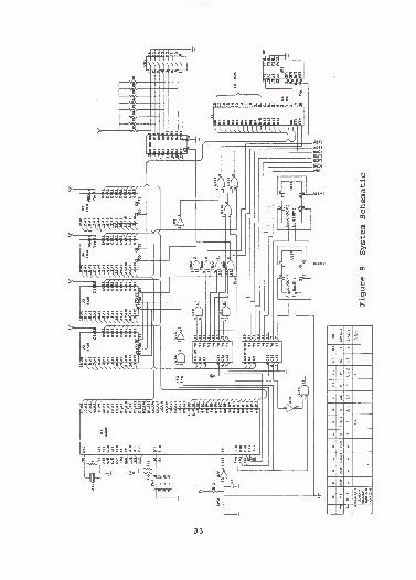
schematic appear in Figures 8 and 9, respectively. As is the
30

usual practice, a despiking capacitor was added between power
and ground for each I.e. These capacitors are not shown on
the schematic, but appear on the parts list in Appendix B.
100
E
X 10
a.
v>
50.1 =
o
0.01 -
TEST CONDITIONS
vCc - svTa - 2S#CCL » SO pF
LSO0 LS00(4 GATES (1 GATE)
MC/HCT00(4 GATES)
HC/HCT00(1 GATE)
1 ' "' ' i»" ' '"I ' ' "i i ii ii
100 1K 10K 100K 1M
FREQUENCY (Hz)
10M 100M
Figure 7 CMOS and LS-TTL Power Consumption-vs-Frequency
A twenty pin edge connector connects the system to the 15-bit
ADC. In actual use another connector would be used to
interface the system to the host computer or alarm device.
The system is broken up into the following sections,
each of which will be discussed: clock, reset and set-up
select, system decoding, read-only memory, random-access
memory, ADC interface, 8-bit port and test I/O, alarm outputs
and system performance. In addition, a section on
synchronous-vs-asynchronous bus protocols is included.
3.2.1 CLOCK, RESET AND SET-UP SELECT
The 20MHz processor clock can be obtained from either an
external clock oscillator connected to input pin Y0 or a
31

crystal oscillator connected between YO and Yl (see
schematic, Figure 9). In the latter case, the clock is
generated by the AAMP's on-chip oscillator. The early system
designs used an external oscillator as shown in Figure 10.
Use of an external oscillator is indicated when the processor
clock is needed in other parts of the system. Since the
final system design does not use the processor clock, the
external oscillator was replaced by a crystal. This change
resulted in a power savings of 76 mW and the two inverters
which were part of the oscillator were eliminated.
CLOCKRESETSET-UP SELECT
V iiADVANCEDARCHITECTUREMICROPROCESSOR
AAMP
DATA
ADDRESS
CONTROL=3
READ-ONLYMEMORY
A II A
SELECT
SELECTANDCONTROL
IIALARMOUTPUTS
RANDOMACCESSMEMORYAAA
ADCINTERFACE
Figure 8 System Block Diagram
32
p
§
oCO
Spw>103
CTN
•H
' 2"4
4 *
3- =
5 ^ -
5 I * ~
5 ^-
s ^ if
? a J
? *-
j
i =-
9*
*
S3 ^
' I
?(
4T
5 i3 "I'll
53s-**
1 i V
33

^>
22pF
1MOHM-AAA/
20MHZ
IC04
YO
1 222pF
Figure 10 External oscillator circuitry
The system's reset circuitry is shown in Figure 9.
Switch 3 (SW3) provides for a manual reset. R12 and CI
provide a high pulse on the Reset line when the input to
inverter U7F is lowered by a manual, power-up or externally
generated system reset. A system reset forces a cold start
(continuation status pointer equal $0000) and the Alarml and
Alarm2 outputs are cleared. The processor reads in the
Executive Entry Table from ROM, as explained in Section
2.2.1, and execution is passed to the Executive
initialization procedure. Since only one task is being
performed, the programs execute entirely in executive mode.
To conserve power and chip count, no switch debouncing was
performed on the manual reset switch. It was shown that the
multiple resets which occur due to the switch bounce do not
affect normal processor function. When the bounce stops the
last reset received will proceed normally and program
execution will begin. Also, under normal operating
34

conditions, most system resets will be generated externally
and received over the system reset line which is a TTL
generated signal.
The set-up select lines SO and SI can be set by two
switches to one of four settings. As detailed in Table 2,
changing the set-up values changes the delay between the
processor's address and R/w lines being valid and the
assertion of Transfer Request. Thus, the select setting
changes the bus cycle length so it can be custom tailored to
the speed of the memory and I/O devices being used, see Table
3 for Bulk CMOS AAMP values. The optimum set-up for the
memories used (150 nS EPROM and 100ns static RAM) was found
to be SI, SO = 0,1. This setting results in a read cycle time
of 500nS and a write cycle time of 550nS (10T and 11T
respectfully, where T is one clock cycle, 50nS.)
Table 3
Max I/O Read/Write response times-vs-set-up select
1,S0 Read time Write time(nS) (nS)
0,0 100 3000,1 150 3001,0 200 3501,1 250 . 350
Very little information about the use of the set-up
inputs was available. The hardware reference manual
indicates that the set-up inputs should be hard wired to
either a "1" or a "0". The set-up select circuitry6
schematic showed that great care must be taken if the set-up
35
is changed while the processor is running. A little
experimentation showed that the set-up time could be changed
while the processor was running and although it was never
implemented, one of the schemes considered to speed up the
system involved changing the set-up depending on the speed of
the device being accessed. It should be noted that the
effect of changing the set-up on overall processor operation
was not investigated. Rockwell was not contacted to verify
proper operation of the AAMP under these conditions since
this speed-up scheme was not implemented.
3.2.2 SYNCHRONOUS-VS-ASYNCHRONOUS BUS PROTOCOL
The AAMP can transfer data either synchronously or
asynchronously, depending upon how the Transfer Acknowledge
(XAK) input signal is generated. If Transfer Request (XRQ)
is tied directly to XAK, the system is in synchronous mode.
The bus cycle length now only depends on the set-up value and
whether the bus cycle is a read cycle or a write cycle. See
Table 4 for Bulk CMOS AAMP values. Asynchronous transfer
mode is in effect when XAK is generated external to the
processor. The internal processor clock will be halted until
the processor receives the XAK signal. Once received, the
processor clock is restarted and the bus cycle continues as
in synchronous mode, subject only to the set-up value and
cycle type.
36
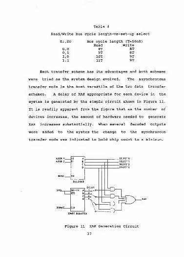
Table 4
Read/Write bus cycle length-vs-set-up select
SI, so
0,00,11,01,1
Bus cycle length (T-50nS)Read Write
8T 8T9T 8T10T 9T11T 9T
Each transfer scheme has its advantages and both schemes
were tried as the system design evolved. The asynchronous
transfer mode is the most versatile of the two data transfer
schemes. A delay of XAK appropriate for each device in the
system is generated by the simple circuit shown in Figure 11.
It is readily apparent from the figure that as the number of
devices increases, the amount of hardware needed to generate
XAK increases substantially. When several decoded outputs
were added to the system the change to the synchronous
transfer mode was indicated to hold chip count to a minimum.
select o
SELECT 1
SELECT J
SELECT 3
XAK
SHIFT IE6ISTEI
Figure 11 XAK Generation Circuit
37
The synchronous transfer mode requires no external logic
to generate XAK. When the processor requests a transfer
(XRQ) an XAK is obtained immediately, the processor clock is
not halted, and the bus cycle continues normally. In this
mode the set-up value is set so that enough delay in the bus
cycle is introduced to allow the slowest device time to
respond to a read or write operation, see Table 3. The AAMP
will run its fastest in synchronous mode with the set-up at
zero (SI, SO 0,0). When byte oriented static RAMS and
EPROMs become available with access times on the order of 50-
75nS the system's performance can be optimized by reducing
the current set-up value of SI, SO = 0,1 to SI, SO 0,0. The
savings on each bus cycle will amount to 50nS.
3.2.3 SYSTEM DECODING
Two 74HC138 3-to-8 decoders were used for system
decoding. Besides ROM and RAM, system devices include a 16-
bit ADC input port and to conform to the existing 8086 system
implementation an 8-bit input port, 7 one-bit outputs which
are simply address decodes and two alarm outputs. The system
memory map is shown in Table 5. All device addresses are the
same as those for the 8086 system except that the locations
of ROM and RAM have been switched. This change was necessary
due to the fact that the AAMP always initializes itself by
reading from locations $0000 to $0008. These locations
contain basic system parameters which must be available upon
power-up (see Table 1 for details on the AAMP's Executive
Entry Table) so the ROM had to be located at address zero.
38

Table 5
System Memory Map
Address (Hex) Purpose
0000-1FFF ROM2000-2FFF ADR13000-3FFF ADR24000-4FFF 8-bit test port
4000-40FF DAC14100-41FF DAC24200-42FF DAC34300-43FF DAC44400-44FF WDT4600-46FF ALARM14700-47FF ALARM2
5000-5FFF 16-bit ADC port6000-7FFF RAM8000-FFFF Unused
Comments
Executive Program MemoryOnly on read cycleOnly on read cycleRead onlyOnly on write cycleOnly on write cycleOnly on write cycleOnly on write cycleActive highActive highActive high
Variable and Data storage
The first decoder (U9, see Figure 9) is enabled whenever
there is an active Bus Request (Er in the low state) . The
second decoder, U12, is enabled only during a write (R/W line
high) to addresses between $4000 and $4FFF. This enable is
generated by the inverter and AND gate (U7A and U6D)
connected to decoder 2's active high enable. The AND gates
(U6B and C) used on the decoder outputs corresponding to ROM
and RAM addresses allow for 8K by 16 bits of ROM and 8K by
16 bits of RAM to be accessed by the system software. The
8086 based system had 4K ROM and 4K RAM, but had left space
in the memory map for the 8K blocks. The two AND gates used
in this addressing scheme were leftover gates and thus became
an economical way to expand the memory and not alter the
memory map.
Since the AAMP is the only device controlling the bus
the BR and BG lines have been tied together. This allows the
39
AAMP to respond immediately to a bus request. Also, since
the AAMP is the only bus master and all software is running
in the Executive mode with no memory partitioning, the other
bus control lines have been left unused or tied to their
inactive state (E/U, C/D, LB, HB, HLD and XER.) In this
implementation the interrupt lines were also left unused.
Depending on the system's actual use in the field the NMI
interrupt would probably see use as a low supply/battery
voltage detector, but since many of the details of the
system's use were not made available by Sandia, IRQ and NMI
were not used.
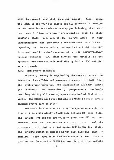
3.2.4 ROM SYSTEM INTERFACE
Read-only memory is required by the AAMP to store the
Executive Entry Table and programs necessary to initialize
the system upon power-up. ROM consisted of two CMOS EPROMs
(UV erasable and electrically programmable read-only
memories) which yield a memory space comprised of 8192 16-bit
words. The EPROMs used were Hitachi's 27C64G-15 which have a
maximum access time of 150nS.
The EPROM interface as shown by the system schematic in
Figure 9 consists simply of AND gate U6B and OR gate U10A.
The EPROMs (U4 and U5) are selected only when BG is low,
address lines A12, A13 and A14 are "000" or "001" and the
processor is initiating a read cycle, R/W in the low state.
The EPROM' s output is enabled at the same time the chip is
enabled. This simplified interface and will not cause a
problem as long as the EPROM has good data at its outputs
40

when the processor enables its data bus. This simple
interface also guards the EPROM against unintentional writes
since the chips are only enabled during a read cycle. Bus
timing for the EPROM with the set-up select at S1,S0=0,1
appears in Figure 12. It should be noted that the timing
diagrams shown here and for the other devices reflect the use
of the SOS AAMP which was used in the system implementation
and not the Bulk CMOS AAMP used for the discussion on bus
timing in the processor architecture section. Of special
note is the additional clock cycle needed for the
synchronization of XAK to the 10MHZ clock. See the
discussion of SOS/CMOS AAMP and Bulk CMOS AAMP differences in
Appendix A. As can be seen from the timing diagram the read
cycle time is 10T or 500nS.
20 MHz
10 MHz
IK & BE
CE & OT
_r
K/W
XRQ & XAK
DATA OUT(worst case)
T=50nS
VALID DATA
j~~l
>XAK sync CPU Read
to 10MHz Clk
Figure 12 EPROM Bus Timing
41

3.2.5 RAM SYSTEM INTERFACE
Random access memory is used to store variables by the
system software. The memory devices selected were Hitachi
8Kx8-bit, low-power, CMOS static RAMS, HM6264LP-10. These
RAMs have a maximum access time of lOOnS and are identified
in the system schematic as U2 and U3. Total RAM storage
available to the system is 8192, 16-bit words which reside at
the top of memory space. See Table 5 for memory map.
The RAMs are selected whenever there is a bus request
and address lines A14, A13 and A12 are "110" or "111". The
RAM data outputs are enabled whenever there is a read
operation regardless of whether the RAMs are selected or not.
This is allowed because if the chips are not selected the
outputs remain in the high-impedance "off" state regardless
of the other control signals. In like manner, a write enable
is generated anytime there is a transfer request and the
processor is in a write cycle by AND gate U6A and inverter
U7C. Several gates are saved by making the RAM's output
enable (0"E) and write enable (RE) "dumb" and controlling
whether the RAMs are on the bus or not with only the chip
enable. The timing diagram for the RAMs with a set-up select
of Si, S 0=0,1 is shown in Figure 13. The read and write cycle
times are 10T (500nS) and 11T (550nS) respectively.
42

20 MHz
10 MHz
W & IC
CTT
XRQ & XAK
W
~i
RAM DATA(worst case)
M & IE
TST
K/W& OT
XRQ & XAK
W
DATA OUT
~L
< VALID DATA
IXAK sync CPU Read
to 10MHz Clk
Write cycle-
< VALID DATA
>
>
Figure 13 RAM Bus Timing
43

3.3 8-BIT PORT AND TEST I/O
To keep the system compatible with the existing 8086
system used by Sandia, an 8-bit input port and seven system
test lines were incorporated into the system design. Owing
to the nature of this system, Sandia did not give details as
to the use of the port and test lines, therefore little was
done with them except to verify that they were functional.
The 8-bit input port consisted of a 74HC373 octal 3-
state noninverting d-type latch, U8. The input lines to this
port were pulled-up to 5 volts using 22k ohm resistors, R2-
R9. This insures that the port will be compatible with TTL
output levels. An octal SPST switch, SW2 , was used to set
the inputs to a known state for test purposes. The system
memory map, Table 5, shows that the port is addressed anytime
there is a Read from any location in the range of $4000-
$4FFF. OR gate U10D is used to combine the correct address
decode and the R~/W line enable the port's output only during
a Read cycle. Bus timing constraints for the port are the
same as for the EPROMs. As tested, the data were already
present and latched when a read cycle occurred so no timing
considerations were involved in port testing.
The seven system test lines are simply generated by
address decodes from decoders U9 and U12 . Table 5 shows the
address ranges given to each line. Each of the test lines is
really an output that is strobed low when addressed. The
length of the pulse is the same as the bus cycle length or
500nS for both read and write cycles. The first two test
44

lines, ADR1 ($2000-$2FFF) and AT5R2 ($3000-$3FFF) , are read
cycle only outputs. OR gates U10B and U10C insure that only
on a read cycle will ADR1 and ADR2 be strobed. The remaining
five test lines and their addresses are: DAC1 ($4000-$40FF)
,
DAC2 ($4100-$41FF) , DXC3 ($4200-$42FF) , T5SU3 ($4300-$43FF)
and WDT ($4400-$44FF) . These lines occupy the same address
space as the 8-bit input port but inverter U7A and AND gate
U6D insure that decoder U12 and thus these test lines are
only enabled on write cycles. The pulse timing of these
lines is the same as for the ADR1 and ADR2 test lines. All
of the test lines except WDT are considered active low. The
WDT line is considered active high.
3.4 ALARM OUTPUTS
The alarm outputs are used to signal the outside world
that the system has detected an intruder. The alarms consist
of two J-K flip-flops, U13A and U13B, corresponding to the
two channels of sensor data. The flip-flops are set up as
on-off toggles. ALARM1 is triggered by a write to addresses
$4600-$46FF. ALARM2 is triggered by a write to addresses
$4700-$47FF (see Table 5) . An alarm stays active until a
system reset is received or until the alarm address is
written to again. Upon power-up the alarms are initialized
to the no alarm state by the reset line.
3.5 ADC INTERFACE
The analog-to-digital converter communicates with the
AAMP through a 20-pin, dual-in-line connector, PI, (see
Figure 9). This connector provides for 15 bits of data, a
45

data ready signal from the ADC and two latch enables to
select which channel of data is selected to be read by the
AAMP. The ADC port is memory mapped into locations $5000-
$5FFF and is made read-only by the combination of the address
decode and the R/W line by OR gate U11A. Inverter U7B and OR
gates U11B and U11C combine to allow channel one data to be
accessed by reading from even addresses and channel two data
to be accessed by reading from odd addresses.
The procedure for reading the ADC's data consists of
several steps. The AAMP's signal processing program enters a
polling routine where the Data Ready signal (bit 15) is
continuously sampled. This is done by reading channel one
(even addresses) which enables the ADC's channel one output
latch and also enables tri-state buffer, U14, allowing the
ADC's Data Ready signal onto the AAMP's data bus. If the
Data Ready signal is high then the data read from channel one
is valid and the AAMP can proceed to read channel two's data
(odd addresses) . The speed of the 15-bit ADC considered for
this implementation was such that little or no wait was
expected in the polling routine, thus system performance will
not suffer and other schemes such as interrupt service
routines can be avoided. It should be noted that the ADC
interface was not implemented, but the design was discussed
with Professor Lenhert (major professor) and Jeff Bradly who
was conducting testing of the 15-bit ADC for Sandia. No
problems were seen with the implementation.
46

3.6 SYSTEM SOFTWARE DESCRIPTION
The main purpose of this project was to implement the
AAMP Digital Signal Processing Unit in minimal hardware while
maintaining maximum system throughput. Since most of the
software groundwork was laid by Ken Albin and Gary
Mauersberger in their respective Theses, the software
implementation for this project was kept simple. The
Standard Fixed-Point Widrow Adaptive Linear Predictor
Algorithm, as coded by Mr. Mauersberger, was chosen as the
signal processing algorithm because of its high execution
speed as compared to the floating point version and the
Widrow' s acceptance by Sandia.
Since there was only one task to perform all software
was run in the Executive mode with Code and Data pointers
equal to zero. Therefore the leading two zeros in the
Executive Entry Table (Table 6) and the Widrow listing
(Appendix D) have been ommitted. Because interrupts were not
used and because the processor was constantly monitored on a
logic analyzer none of the routines provided for by the
Executive Entry Table (Bus Error Interrupt, Maskable,
Nonmaskable Interrupts, Trap and Exception) were implemented.
In a system out in the field most of these routines would be
needed to protect the system from hardware and software
errors such as low-power conditions and arithmetic overflow
and underflow.
47

Address Dat(hex)0000 00000001 7F000002 7FF00003 00200004 00000005 00000006 00000007 00000008 0000
Table 6
System Executive Entry Table
Description
Continuation Status Pointer (PTR)
Initial EXEC. Stack Limit (PTR)Initial EXEC. Top-of-Stack (TOS)Widrow Procedure ID (PROCID)Bus Error Interrupt (PROCID)Nonmaskable Interrupt (PROCID)Maskable Interrupt (PROCID)Trap (PROCID)EXEC. Exception (PROCID)
(PTR)
Upon reset the system reads the Executive Entry Table
from ROM, sets up the Executive Process State Descriptor
Table and Executive Stack (see sections 2.2.3 and 2.2.4) and
transfers control to the Widrow signal processing program.
If an error occurs in the program or in the hardware that
requires the service of one of the Executive Entry Table
routines the processor will halt since none of these programs
exist as defined by a zero in their PROCID.
48

4.0 SYSTEM PERFORMANCE
System performance is measured by how well the system
goals are met. These goals can be divided into three areas:
1) system power consumption, 2) system throughput and 3)
compatibility to existing system used by Sandia. Each of
these three areas will be addressed.
4.1 SYSTEM POWER CONSUMPTION
System power consumption data was taken with the Widrow
signal processing program running in an infinite loop and
appears in Table 7. Data were taken at three different set-
up select settings to see how bus cycle length affected the
power consumption. Power consumption when the processor was
reset was also recorded.
Table 7
System Power Consumption (at 20 MHz)
Set-up Select(SI, SO)
0,11,01,1
Reset
Power Consumptionwith externaloscillator
248. OmW245. 5mW236. OmW
110. OmW
Power Consumptionwithout externaloscillator
171. 5mW168. 5mW169. OmW
32. OmW
The goal for the entire signal processing system (AAMP
signal processing unit and 15-bit bipolar ADC) was set at
7 5 OmW. The ADC under consideration uses approximately 4 OmW.
Therefore the AAMP and ADC together consume about 212mW or
72% under the specification (Si, so =0,1 and no external
49

oscillator) . In addition, these values can be seen as a
worst case figure for two reasons: 1) as will be shown in the
next section the AAMP does not need to be run as fast as 20-
MHZ to meet system performance specifications and 2) smaller
than 8K byte ROMs and RAMs could be used saving a
considerable amount of power.
In addition to low-power consumption the system's
objectives were also to minimize part count and limit board
space. By simplifying the memory interface and using
existing, unused gates to implement functions instead of
additional chips, i.e. using a spare inverter and AND gate
instead of a NAND gate, part count was minimized. The board
size was specified to be a 4" by 7" multilayer board. Since
the wire wrap layout was on a 4.5" by 6" board with extra
room left over, a board layout was not attempted. Considering
the low number of parts involved, no problem meeting this
specification was foreseen.
4.2 SYSTEM THROUGHPUT
To measure maximum system throughput the Widrow signal
processing software was run in an infinite loop with no wait
states for data (ADC) input. A counter was tied to the ADC
latch enable and a maximum samples/sec was obtained. Again
data were taken for all applicable set-up select states. As
is plainly shown in Table 8 the system specification of
sampling two channels data at 128 samples/sec is easily met.
The minimum number of samples/sec needed is 2*128 samples/sec
or 256 samples/sec.
50

Table 8
System Throughput
Set-up Select Samples/sec(SI, SO)
0,1 8691.0 7801.1 706
4.3 SYSTEM COMPATIBILITY
As stated in the system specifications, the AAMP system
is to be as close to the existing 8086 system as possible
with respect to I/O configuration and memory map. This goal
was satisfied with the exception of the location of the ROM
and RAM in the memory space. The 8086 system located ROM at
the top of memory and RAM at the bottom, but due to the fact
that the AAMP requires its Executive Entry Table to be in
locations 0-8 in memory, the ROM and RAM locations were
switched on the AAMP system. This change should cause a
minimal amount of change in Sandia's system and software test
procedures
.
51

5 . CONCLUSIONS
The AAMP based signal processing unit proved to be an
exceptionally easy to design and high performing
microprocessor based system. All system design objectives
were met and in the important category of power consumption
the AAMP based system performed remarkably well. The
nonmultiplexed address and data busses along with the
synchronous or asynchronous bus protocols makes the AAMP easy
to interface into a system and reduces part count. The user,
in arranging system hardware and software, is provided
maximum flexibility by the AAMP.
The only problems encountered in system development
concerned how to minimize system hardware while providing
adequate protection for system resources. This problem was
easy to solve by virtue of the easy interface with todays
modern static RAMs and EPROMs.
The high level language orientation of the AAMP combined
with the hardware implementation of math functions such as
floating point multiply and divide make the AAMP a natural
choice for signal processing implementations and when the
Bulk CMOS version of the AAMP becomes generally available its
use in many high performance applications will establish it
as a major microprocessor to contend with processors such as
the 80286 and 68000.
52

Acknowledgements
This research was sponsored by the Base and Installation
Security Systems Program Office, Electronics Systems Division
of the Air Force Systems Command, Hanscom Air Force Base, MA
01731 through the Engineering Division 5238, Sandia National
Laboratories, Albuquerque, New Mexico.
I would like to give special thanks to Dr. Donald H.
Lenhert for his seemingly infinite patience with me as I
worked my way into the Engineering profession. Thanks are
also extended to Dr. M.S. P. Lucas and Dr. Maarten van Swaay
for serving as committee members and to my wife who thought
this would probably never end but stuck with me nonetheless.
53
References1Kenneth L. Albin, "An Evaluation of Rockwell's Advanced
Architecture Microprocessor for Digital Signal ProcessingApplications" (MS Thesis, Kansas State University, 1984).
2Gary S. Mauersberger, "The Design and Hardware
Evaluation of an Advanced 16-bit, Low-power, High-performanceMicrocomputing System for Digital Signal Processing"(MS Thesis, Kansas State University, 1985)
.
3
AAMP Hardware Reference Manual, RockwellInternational , 1984
.
4AAMP Architecture Reference Manual , Rockwell
International , 1984
.
5QMOS High-Speed CMOS Logic ICs , RCA, 1983, pg 18.
6Dave W. Best, "Design of an Advanced Architecture
Microprocessor" (MS Thesis, Iowa State University, 1984),pp 109-110.
54

Appendix A
CMOS-vs-SOS/CMOS Versions of theAdvanced Architecture Micropressor (AAMP)
55

CMOS-vs-SOS/CMOS Versions of theAdvanced Architecture Microprocessor (AAMP)
The two-micron SOS/CMOS version of the AAMP used in the
implementation of this project is currently being phased out
in favor of a Bulk CMOS version. The Bulk CMOS version is
not pin-for-pin compatible with the SOS/CMOS version. Table
Al lists pinout changes. In addition to the functional
changes, several internal timing changes were also made. The
importance of these changes to this project is the effect
they will have on system implementation with the new
processor. After the pin changes are outlined, any
modifications that would be required to the system
implementation will be discussed.
Table Al
Pin-out Changes to the AAMP
iction Bulk CMOS Function
VDDGNDSOUT*L/S*
SCLK*SIN*NCNC
GND
Denotes a pin that is used for device testing only.Not connected during normal use.
NC Not connected. Do not connect these pins.
Pin Number sos/cmos :
Fl NCL2 NCL7 NCK7 NCK9 NC
L10 NCKll HLDHll HBH10 EbA5 NC
*
56

As can be seen in the table, several additional
functions have been added to the AAMP by using pins that were
previously unused. Four test pins have been added, but these
pins are only used for testing the AAMP itself. The
processor hold function (HLD) and the high-byte, low-byte
indicators (HTJ and TB) have been deleted in the new version
of the AAMP. These pins were not used in this implementation
so no changes are necessary. The low-byte indicator has been
changed into an output enable (61) . This input allows the
Bulk CMOS AAMP to bring its address, data and control busses
into a high impedance state making it much easier to
interface the AAMP into multiple master systems. In this
system, the AAMP is the only bus user, so the 51 (LB on
SOS/CMOS AAMP) pin will have to be tied to ground instead of
open as it is in the present implementation. The other pin
changes that will require attention are the addition of
another power pin (VDD pin Fl) and two additional ground pins
(A5 and L2) . These pins are not connected in the present
system so they will have to be tied to the appropriate logic
level
.
Several other changes have been incorporated into the
Bulk CMOS AAMP. A built in 50nS hold time after XRQ goes
"low" for addess, data, E/W, E/U and C/D has been added. In
the present SOS version of the AAMP the hold line (HLD) could
be controlled by external devices to accomplish this same
purpose. Transfer acknowledge synchronization has also been
changed. Synchronization will be to the 20 MHz clock for the
57

new version instead of the 10 MHz clock in the SOS/CMOS
version. These changes will act to reduce bus transfer cycle
times. Although this system was originally designed to
operate with the Bulk CMOS AAMP it is readily evident from
the above discussion and the EPROM bus timing diagram of
Figure 12 that the 150nS EPROMs used in this implementation
would not be fast enough. A switch to 120nS or faster EPROMs
would be needed to use the Bulk CMOS AAMP with a set-up
select (0,1)
.
To make the Bulk CMOS AAMP easier to interface into
larger systems the fanout of each output pin has been
increased. As of this writing the exact fanout has not been
determined. Both the SOS and Bulk CMOS versions of the AAMP
are TTL compatible.
Overall, very few changes in system implementation will
be necessary to adapt the system to the new Bulk CMOS version
of the AAMP. Except for a slightly increased power
consumption in the new version, the changes can be seen as
improvements to the existing chip design and in many systems
will make implementation much easier.
58

Appendix B
Parts List and Board Layout
59

AAMP Signal Processing UnitParts List
Description
lOuF 25V Tantalum capacitor1M ohm 5% 1/4W carbon resistor47K ohm 5% 1/4W carbon resistor22K ohm 5% 1/4W carbon resistor3.3K ohm 5% 1/4W carbon resistorRE-AL-INC Quad SPST dip switchCTS Octal SPST dip switchALCO SPST momentary push switchAdvanced Architecture uP8K by 8-bit Static RAM8K by 8-bit Static RAM8K by 8-bit EPROM8K by 8-bit EPROMQuad two-input AND gateHex inverterOctal transparent latch3-to-8 line decoderQuad two-input OR gateQuad two-input OR gate3-to-8 line decoderDual J-K Flip-Flop with ResetQuad 3-state Noninverting buffer20MHz crystal20-pin wire wrap edge connector0.01 uF despiking caracitorBanana Jacks4.5"X6" perf board
between Vcc (5V) and ground.
All I.C.'s installed in wire wrap sockets notincorporated into parts list.
Reference Part Number
CI UNKNOWNRl UNKNOWN
R2-R9 UNKNOWNR10-R11 UNKNOWN
R12 UNKNOWNSW1 UNKNOWNSW2 206-8-730SW3 AP1C24Ul AAMPU2 HM6264LP-10U3 HM6264LP-10U4 HM27C64G-15U5 HM27C64G-15U6 MC74HC08NU7 SN74HC04NU8 MC74HC373NU9 MC74HC138NU10 MC74HC32NUll MC74HC32NU12 MC74HC138NU13 MC74HC73NU14 MC74HC125NXTL 07XTL20.00HHPI 52-1120-50
(14 parts) A5C103K(2 parts) UNKNOWN(1 part)
Notes: Desr>iking capacito
60
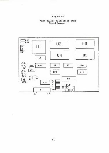
Figure Bl
AAMP Signal Processing UnitBoard Layout
[10I IR11
ESWl
©5V
U1
U9
& U12
XTL
6ND n20 D=
SW3
U2
U4
U7
U13
U14
P1
R2
R9 ' '
U6
U8
V V
SV2d~od nD DDD
U3
U5
U10
U11
61

Appendix C
"Stripped Down" AAMPSignal Processing Unit
62

"Stripped Down" AAMP Signal Processing Unit
The "stripped down" AAMP Signal Processing Unit is the
result of Sandia wanting an AAMP based system with a minimum
of "bells" and "whistles". Basic system requirements are the
same as for the larger system but the I/O requirements were
greatly reduced. The over-riding goal of this project was to
design a system with absolute minimum power requirements and
board space. To this end, the only system requirements were
that the system still process two channels of data, at 128
samples/sec and provide an alarm output for each channel.
Memory space could be minimized and the system clock speed
could be reduced to the minimum consistent with system
requirements.
The system schematic appears in Figure CI. As the
schematic shows, the reduction of required I/O greatly
reduces the amount of hardware needed to make the system
work. Only one "glue" chip is needed to interface the AAMP
to the system memory. The memory interfacing scheme is the
same one used in the larger system, but the choice of smaller
memory devices (2KX8 bits static RAM and 4KX8 bits ROM)
requires only one decoder output to utilize the full memory
space. The two latches shown are actually on the ADC board
and are enabled directly by the system decoder allowing ADC
data onto the AAMP's data bus. The alarm outputs are
implemented the same as before with the only difference being
their location in the memory map, see Table CI. To reduce
part count further, the set-up select inputs were hard-wired
63

ooodooo
5 s
^ffffffi
5?
mm*i
s >
E O o a 1 D o i
= ?
^^^Mi^iiiMiiiiigBaaa^B
HOP
SimHi-
^sA
itiMJ
iH' 1
cDtPc•Hin
tn
0)
uou
10
c
•Hw
sc
aTS0)
ftau
w
u
u
-HCm
64

to SI, SO = 0,0 and the manual reset was removed.
Table CI
"Stripped Down" AAMP System Memory Map
Address (Hex) Purpose
0000-07FF ROM1000-1FFF ADC2000-2FFF ADC3000-4FFF UNUSED5000-5FFF ALARM16000-6FFF ALARM27000-7FFF RAM8000-FFFF UNUSED
Comments
Executive Program MemoryChannel 1 latch enableChannel 2 latch enable
Channel l's alarm outputChannel 2's alarm outputVariable and Data storage
PERFORMANCE
Due to time constraints this system was never actually
tested. To determine the lower limit on operating frequency
various crystals were tried on the large system and a 4MHz
operating frequency was found to be about as slow as the
system could run and still be able to sample two channels of
data at 128 samples/sec. To estimate power requirements, the
large system was run at this lower speed (4MHz) and
unnecessary chips were removed. The savings in power
afforded by smaller, slower ROMs and RAMs was estimated and
the resulting power estimate was 80-100mW.
CONCLUSION
The "Stripped Down" AAMP Signal Processing Unit looks as
if it fulfills all of its design goals. The basic operation
has been throughly tested with the larger system and there
seems to be room for improvement in the already low power
consumption figure by switching to even smaller memories,
such as 2KX8-bit ROMs. This system, with only nine IC's,
65

could probably be put on the ADC board thus saving a great
deal of expense while making the system smaller and more
reliable.
66

Appendix D
Widrow Adaptive Linear Predictive AlgorithmListing
67

Widrow Adaptive Linear Predictor Algorithm Listing
This appendix contains the object code listing for the
Standard Fixed-Point Widrow Adaptive Linear Predictor
Algorithm. The program resides in Executive space and the
reader is referred to the Executive Entry Table (Table 6) for
processor set-up. For a better understanding of the Widrow
Algorithm the reader is -referred to the work done by Mr.
Albin and Mr. Mausersberger. The comment section of the
listing outlines the algorithm as given by Mr. Mauersbeger in
his thesis.
Address Contents Opcode Instruction Comments
1020 0036 0036 Procedure header1021 4410 10 LIT4A.0
44 ASNSL.4 q =1022 5C11 11 LIT4A.1
355C ASNSLE k = 1
1023 1E35 351E REFSLE get k1024 1835 1018 LIT81025 EC10 EC GR is k > 16?1026 1D5B 1D5B SKIPNZ X jump to $1035 if true1027 1E10 10
351ELIT4A.0REFSLE
1028 1435 14 LIT4A.41029 A653 53 LOCL
A6 ASNSX b-array(k) =102A 1E10 10
351ELIT4A.0REFSLE
102B 1835 1418 LIT8102C 5314 53 LOCL102D 10A6 A6
10ASNSXLIT4A.0
f-array (k) =
102E 351E 351E REFSLE102F 2418 2418 LIT81030 A653 53 LOCL
A6 ASNSX e-array(k)1031 351E 351E REFSLE get k1032 E411 11 LIT4A.1
E4 ADD -
1033 355C 355C ASNSLE k «= k + 1
1034 2319 2319 LIT8N1035 1C59 59 SKIP jump to $1023
68

1036 6000 60001C REFSI get DAC data at $60001037 1041 41 ASNSL.l f - DAC data
DO REFSX get b-array(k)1041 1835 351E REFSLE1042 5314 1418
53LIT8LOCL
1043 F9D0 DOF9
REFSXMPY
get f-array(k)
1044 42E4 E4 ADD42 ASNSL.2 g - g + b-array(k) *
f-array(k)1045 351E 351E REFSLE get k1046 E411 11
E4LIT4A.1ADD
1047 355C 35D0 REFSX get b-array(k)1041 1835 351E REFSLE1042 5314 1418
53LIT8LOCL
1043 F9D0 DOF9
REFSXMPY
get f-array (k)
1044 42E4 E4 ADD42 ASNSL.2 g - g + b-array(k) *
f-array (k)
1045 351E 351E REFSLE get k1046 E411 11
E4LIT4A.1ADD
1047 355C 355C ASNSLE k = k + 11048 1E19 1E19 LIT8N1049 0159 59 SKIP jump to $103F
01 REFSL.l get f104A E502 02
E5REFSL.2SUB
get g
104B 1143 4311
ASNSL.3LIT4A.1
e = f - g
104C 355C 355C ASNSLE k = l
104D 351E 351E REFSLE get k104E 1018 1018 LIT8104F 5BEC EC GR is k > 16?1050 1A24 245B SKIPNZ I jump t $1067 if true1051 7C00 7C001A LIT16 u = 0.986751052 351E 351E REFSLE1053 5314 14
53LIT4A.4LOCL
1054 F9D0 DOF9
REFSXMPY
get b-array(k)
1055 001A 04001A LIT16 v = 0.031251056 0304 03 REFSL.3 get e1057 1EF9 F9 MPY1058 1835 351E REFSLE1059 5314 1418
53LIT8LOCL
105A F9D0 DOF9
REFSXMPY
get f-array(k)
105B 1EE4 E4 ADD
69

105C 1435 351E14
REFSLELIT4A.4
105D A653 53 LOCLA6 ASNSX b-array(k) » u *
b-array(k) + v *
e * f-array(k)105E 351E 351E REFSLE get k105F E411 11
E4LIT4A.1ADD
1060 355C 355C ASNSLE k = k + 1
1061 2A19 2A19 LIT8N1062 0359 59 SKIP jump to $1052
03 REFSL.3 get e1063 B814 14
B8LIT4A.4ARS
1064 436A 6A DUP43 ASNSL.3 • - e / 16
1065 1E04 04 REFSL.4 get g1066 E534 341E
E5REFSLESUB
get e-array(16)
1067 44E4 E4 ADD44 ASNSL.4 q m g - e-array(16) + e
1068 0404 04 REFSL.4 get g04 REFSL.4 get g
1069 54F9 F9 MPY q * q106A 5001 500154 ASNSI output result, for test
only106B 2F20 20
2F
LIT4B.0
LIT4B.F
dummy statement, noeffect
106C 355C 355C ASNSLE k = 15106D 351E 351E REFSLE get k106E EB10 10 LIT4A.0
EB EQ is k = 0?106F 215B 215B SKIPNZ I jump to $1089 if true1070 351E 351E REFSLE1071 2418 2418 LIT81072 D053 53 LOCL
DO REFSX get e-array(k)1073 351E 351E REFSLE1074 2518 2518 LIT81075 A653 53 LOCL
A6 ASNSX e-array(k + 1) =
e-array(k)1076 351E 351E REFSLE1077 1418 1418 LIT81078 D053 53 LOCL
DO REFSX get f-array (k)1079 351E 351E REFSLE107A 1518 1518 LIT8107B A653 53 LOCL
A6 ASNSX f-array(k + 1) =f-array(k)
107C 351E 351E REFSLE get k
70

107D E511
107E 355C107F 26191080 0359
1081 255C1082 5C011083 1915
1084 599E1085 36181086 005F
11 LIT4A.1E5 SUB
355C ASNSLE k «= k - 12619 LIT8N
59 SKIP jump to $107603 REFSL.3 get e
255C ASNSLE e-array(l) « e01 REFSL.l get f
155C ASNSLE f-array(l) « f9E19 LIT8N
59 SKIP jump to $10353618 LIT8
5F RETURN procedure end
Local Variable Memory Map
Local Environment Offset Variable
1 f2 g3 e4 q5 - 14 b-array15 - 24 f-array25 - 34 e-array35 k
71

THE DESIGN AND IMPLEMENTATION OF A 16-BIT,LOW-POWER, HIGH-PERFORMANCE, MICROPROCESSOR BASED
DIGITAL SIGNAL PROCESSING UNIT
by
Michael D. Gaches
B. S., Kansas State University, 1984
AN ABSTRACT OF A MASTER'S THESIS
submitted in partial fulfillment of the
requirements for the degree
MASTER OF SCIENCE
Department of Electrical and Computer Engineering
KANSAS STATE UNIVERSITYManhattan , Kansas
1987

This thesis is a design and implementation of a low-
power, high-performance microprocessor based system for
signal processing applications using Rockwell International's
Advanced Architecture Microprocessor (AAMP) . This work is
part of an ongoing program by the Electrical and Computer
Engineering Department at Kansas State University to evaluate
low-power, high-performance microprocessors.
The AAMP is a 16-bit, CMOS processor which operates from
a 20MHz clock. The instruction set and architecture are well
suited for the use of high level languages. Features include
double precision, floating-point arithmetic, hardware
multiply and divide and extensive support for procedure
handling, context switching and task management.
This thesis covers the AAMP's operating characteristics,
the development of the microprocessor system and the
evaluation of the system's performance in relation to a set
of system specifications intended to yield a system with
extremely low power consumption (suitable for battery
operation) , high system throughput and minimal real estate
and part count. Standard signal processing algorithms
previously evaluated on the AAMP will be used to measure
system throughput and power consumption will be monitored at
various processing speeds. A system that has reduced input,
output and memory requirements will then be designed in the
hope of creating a system that is even smaller and lower in
power consumption but still retains the specified system
throughput.