design and fabrication of plasma enhanced atomic layer...
TRANSCRIPT

3 Design and Fabrication of Plasma Enhanced
Atomic Layer Deposition System (PEALD)
The first step towards accomplishing the objectives of present work is the
design and fabrication of an ALD system and establishment of operating
conditions to achieve deposition in ALD mode. This chapter gives the basics
of atomic layer deposition and design, fabrication and optimization of the
home made ALD system in detail.
3.1 Introduction
The design of a new system is the result of an engineer’s imagination,
shaped by a long list of known requirements and limitations of costs and
construction. Several design revisions eventually result in the construction of
an experimental system. During the fabrication and testing of an
experimental system, the list of requirements is extended with (some)
previously unknown items. In a research project with only one possibility to
construct an experimental system, the challenge is to look beyond the newly
found design requirements and focus on the research issues.
The semiconductor technology node is now undergoing a transition to 22nm
and smaller dimensions. The thickness of the gate dielectric must also
decrease with the decrease in gate length. The current trend in integrated
circuit (IC) manufacturing, to decrease feature sizes while increasing aspect
ratios and complexity, requires process control at atomic level. This can be
easily attained by ALD. The drive for shrinking device dimensions has
indeed contributed to the development of ALD which is presently
experiencing major design breakthroughs. Already ALD has emerged as the
method of choice for demanding applications [1]. This is evident from a
rapidly increasing number of new materials, processes and reactor designs as
well as users in both industry and academia.
48 Chapter 3
3.2 Atomic Layer Deposition (ALD)
ALD is a modified form of chemical vapour deposition technique (CVD)
based on alternating saturative surface reactions. As distinct from the
chemical vapour deposition technique, in ALD the precursor vapours are
pulsed into the reactor alternately, one at a time, separated by purge or
evacuation. Each precursor exposure step saturates the surface with a
monolayer of that precursor. The monolayer thickness is dependent on the
reactivity of the precursor with the surface. This results in a unique self-
limiting film growth mechanism with a number of advantageous features,
such as excellent conformality, uniformity, and simple and accurate film
thickness control.
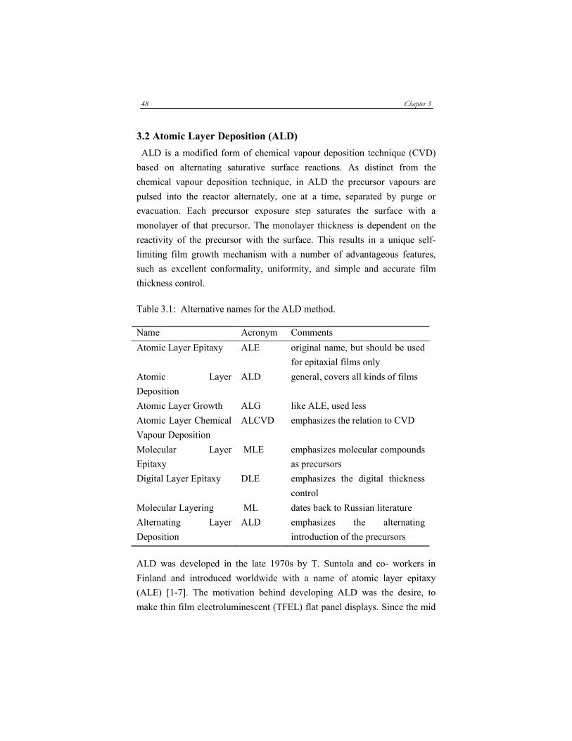
Table 3.1: Alternative names for the ALD method. Name Acronym Comments
Atomic Layer Epitaxy ALE original name, but should be used
for epitaxial films only
Atomic Layer
Deposition
ALD general, covers all kinds of films
Atomic Layer Growth ALG like ALE, used less
Atomic Layer Chemical
Vapour Deposition
ALCVD emphasizes the relation to CVD
Molecular Layer
Epitaxy
MLE emphasizes molecular compounds
as precursors
Digital Layer Epitaxy DLE emphasizes the digital thickness
control
Molecular Layering ML dates back to Russian literature
Alternating Layer
Deposition
ALD emphasizes the alternating
introduction of the precursors
ALD was developed in the late 1970s by T. Suntola and co- workers in
Finland and introduced worldwide with a name of atomic layer epitaxy
(ALE) [1-7]. The motivation behind developing ALD was the desire, to
make thin film electroluminescent (TFEL) flat panel displays. Since the mid

Design and Fabrication of PEALD system 49
1990s, interest in ALD technology has increased rapidly in the silicon-based
microelectronics industry. This interest is a direct consequence of the ever-
decreasing device dimensions and the increasing aspect ratios in integrated
circuits (IC). Traditional thin film deposition techniques such as chemical
vapour deposition (CVD) and physical vapour deposition (PVD) are
expected to meet major conformality problems during the next few years and
now ALD is considered as a promising alternative candidate. At the same
time, film thicknesses are shrinking so that ALD’s major drawback, the low
deposition rate, is becoming less important [8].
3.2.1 ALD cycle
In ALD, the film growth takes place in a cyclic manner. In the simplest case,
one cycle consists of four steps:
(i) Exposure of the first precursor
(ii) Purge by gas flow, or evacuation of the reaction chamber
(iii) Exposure of the second precursor
(iv) Purge by gas flow or evacuation of the chamber
This cycle is repeated as many times as necessary to obtain the desired film
thickness.
Figure 3.1 illustrates sequence scheme for a simple two precursor
ALD cycle with each cycle consisting of four steps. (i) Exposure of
precursor #1 which reacts with the surface in a saturating manner until a
monolayer has been chemisorbed and no further adsorption take place. Since
the reaction stops when one mono layer is formed, the process is called ‘self-
limiting’. (ii) Excess precursor and by-product is then evacuated or purged
out. (iii) Exposure to precursor #2 leads to a reaction of precursor #2 with
the already adsorbed mono layer of precursor # 1 on the surface in a second
self-limiting reaction, thus depositing a second layer of atoms onto the first.
The second reaction must also return the surface to a state in which it is
ready to react with the first reactant. (iv) This is followed by another
evacuation or purge. Additional reactants having suitable complementary

50 Chapter 3
self-limiting reactions can be used to form ternary compounds, doped
compounds, graded compositions, or nanolamination that can show
properties that are dramatically improved over homogeneous materials [7-
12].
Figure 3.1: Schematic of an ideal four-step, two precursors ALD cycle.
The self-limiting growth mechanism gives ALD a number of advantageous
features such as [6,12]:
� accurate and simple thickness control
� large-area and large batch capabilities
� excellent conformality
� no problems with varying vaporization rates of solid precursor
� good reproducibility
� straightforward scale-up
� capability to produce sharp interfaces
� favours precursors highly reactive toward each other, thus enabling
effective material utilization and short cycle times
� high quality materials can be obtained at low processing
temperatures
� capability to prepare multilayer structures (nano-laminates) in a
continuous process
Most of the ALD processes reported are based on the above described
exchange reactions between molecular precursors. Another possible reaction
Design and Fabrication of PEALD system 51
type is additive with elemental precursors but because only a few metals are
volatile enough, the applicability of these reactions is limited. A quite rare
third reaction type, as well, involves a self-limiting adsorption of a precursor
followed by its decomposition by an appropriate energy pulse or by its
reduction using an appropriate reductant. In a majority of the ALD processes
reported, the reactions are activated thermally under isothermal conditions.
The alternate pulsing or separate dosing of reactants is definitely the most
characteristic feature of ALD and almost distinctive as the self-limiting
growth mechanism of one monolayer. A common misconception is that
ALD growth always proceeds in a layer-by-layer manner, but this is often
not the case as only a fraction of a monolayer may be deposited practically
in each cycle. Reasons for the less than a monolayer per cycle growth are the
limited number of reactive surface sites and the steric hindrance between
bulky ligands in the chemisorption layer [9]. Another important
characteristic feature of ALD is its wide range of processing temperature
window [12].
3.2.2 Variance of ALD
Though ALD was originated as a thermal method, several
modifications were added as time passed. All the objectives were towards
improving the film characteristics and lowering the deposition temperature.
Two major ALD methods are thermal ALD and plasma assisted ALD.
Thermal ALD
Thermal ALD is the most researched type of ALD, because it mostly
resembles CVD whereas the hardware configuration is also relatively
simple. It typically consists of a heated vacuum chamber in which substrates
are coated by the alternate pulsing of precursor vapours, separated by purge
gas flows. The whole ALD processing cycle can often be regarded as a sort
of “pulse-train”, commonly referred to as “travelling wave”. This pulse-train
starts at one end of the reactor moves over the substrate surface, where
deposition occurs, and disappears into the pump at the other end. Two
reactor concepts currently exist: the cross flow concept, where the flow of
precursors is parallel to substrate surface; and the perpendicular flow

52 Chapter 3
concept, in which the precursors are introduced from the top of the reactor
and flow perpendicular towards the substrate going downwards into the
pump.
Figure 3.2: Thermal ALD reactor using cross flow concept.
Radical enhanced ALD
In Radical enhanced ALD, Thermal ALD hardware is adapted to
include a remotely placed radical source. Plasma is created in the source at
low pressure (<1.33mbar ) from a source gas, most commonly being O2, N2,
H2, and mixtures thereof. It is attempted to deliver the generated radical
species to the substrate surface, in a similar fashion as a normal precursor
vapour dosing would be performed, i.e. via a tubular inlet.
Figure 3.3: Radical enhanced ALD using microwave concept.
Direct plasma ALD
A common plasma configuration is the parallel plate concept, as
shown in Fig. 3.4. The plasma is generated in between two parallel placed

Design and Fabrication of PEALD system 53
electrodes that are spaced ~1-5 cm apart, from a source gas at low pressure
(1-0.013 mbar).
Figure 3.4: Direct Plasma ALD reactor using HVDC power
A RF (or a high voltage DC of the order of 1kV is applied, in this
case called DC plasma) voltage is applied to the top electrode. The substrate
is residing on the lower, grounded counter-electrode, and the substrate plays
‘directly’ a role in the plasma generation. To improve the uniformity of the
plasma, the top electrode commonly consists of a showerhead gas
distributor, through which source gases is fed into the plasma chamber. For
the same reason, in some cases, the precursor is fed through the same
showerhead.
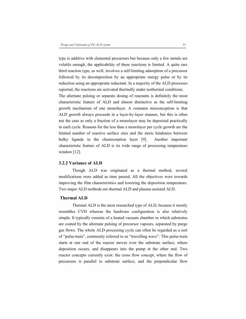
Remote plasma ALD
Plasma is not in direct contact with the substrate in the remote
plasma ALD. The configuration with a RF source for plasma is shown in
figure 3.5. The distance between the plasma source and the substrate is few
tens of cm. Figure 3.5 shows the schematic diagram of remote plasma set up.
54 Chapter 3
Figure 3.5: Remote Plasma ALD.
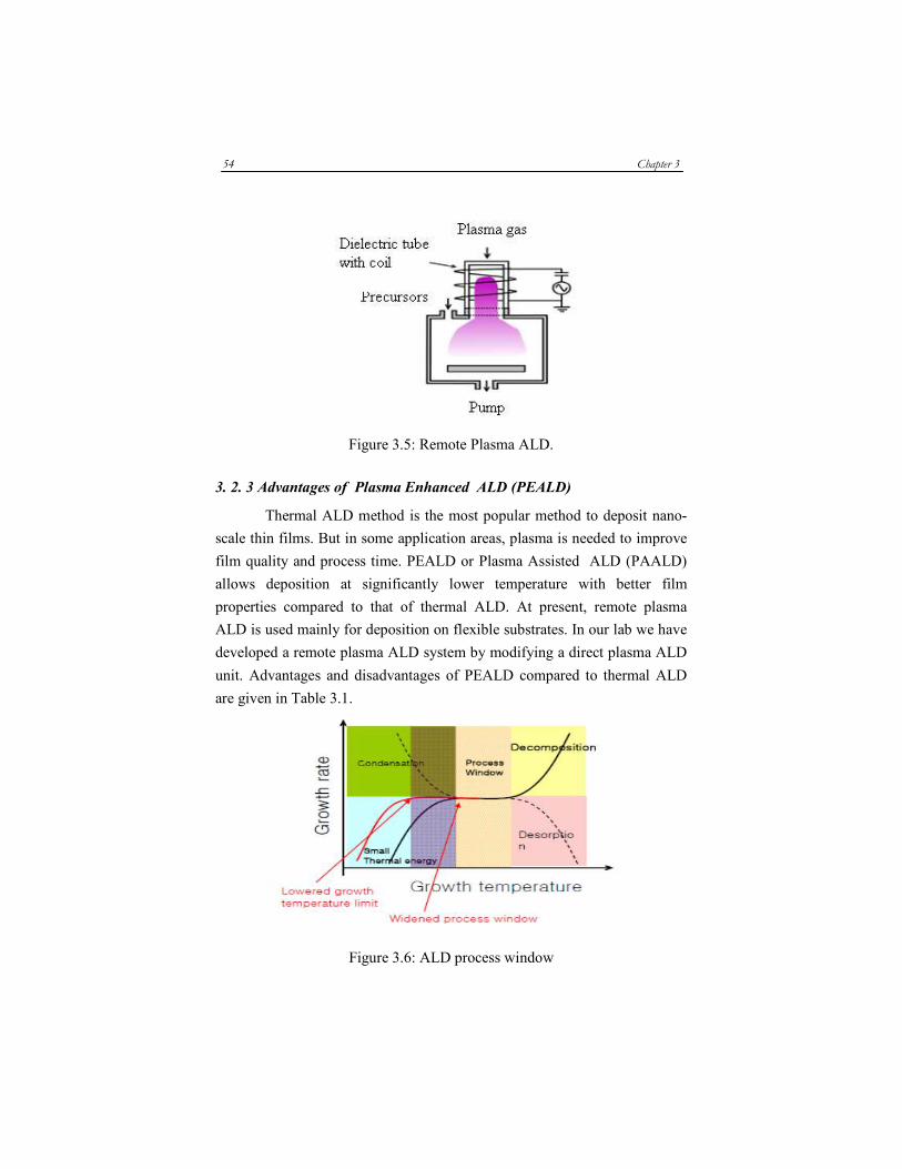
3. 2. 3 Advantages of Plasma Enhanced ALD (PEALD)
Thermal ALD method is the most popular method to deposit nano-
scale thin films. But in some application areas, plasma is needed to improve
film quality and process time. PEALD or Plasma Assisted ALD (PAALD)
allows deposition at significantly lower temperature with better film
properties compared to that of thermal ALD. At present, remote plasma
ALD is used mainly for deposition on flexible substrates. In our lab we have
developed a remote plasma ALD system by modifying a direct plasma ALD
unit. Advantages and disadvantages of PEALD compared to thermal ALD
are given in Table 3.1.
Figure 3.6: ALD process window

Design and Fabrication of PEALD system 55
Table 3.1: Characteristic advantages of Remote Plasma ALD
Advantages Disadvantages
Lower deposition temperature More complicated chamber design
Broader no. of chemistry -
possible
More complicated reaction -
chemistry
Denser films Potentially poor conformality
Higher throughput Slower (not always)
In situ plasma treatments Damage to films (not always )
Lower impurity Additional growth parameters
Growth characteristics of PEALD are shown in Figure 3.6. When
the ALD process is performed at temperatures which provide sufficient
thermal energy for chemical reactions, the growth rate usually remains
constant. This temperature range is often called the ‘ALD process window’.
This nearly constant growth rate for a range of growth temperature during
ALD provide better reproducibility in film thickness than other film
deposition methods, such as chemical vapour deposition. However, at
growth temperatures greater than this temperature range, the growth rate
usually increases, caused by disturbances in the self-limiting process due to
thermal decomposition of the precursor. However, for a few material
systems, the growth rate decreases with increasing growth temperature
which may be due to reduction in adsorption site density on the depositing
surface.
The use of plasma generally reduces the growth temperature due to
the high reactivity of radicals in the plasma. Due to lowered growth
temperature the process window is effectively widened (Figure 3.6). There is
a high degree of versatility in the materials used for PEALD. This is due to
the high reactivity of radicals generated, which allows to perform many
chemical reaction schemes which are impossible with thermal ALD. These
two advantages make the remote plasma based technique superior than
thermal ALD.

56 Chapter 3
3.3 ALD precursors
Chemical film deposition processes are controlled by the choice of
source materials. The chosen precursor can exist in the solid state, as liquids
or in the vapour state. The choice of precursors is the key issue in a
successful design of an ALD process. The main requirements for ALD
precursors are [12]
• Volatility
• No self decomposition
• Aggressive and complete reactions
• No etching of the film or substrate materials
• Easy to synthesis and handle
• Un-reactive volatile by-products
• Sufficient purity
• Inexpensive
• Non-toxic and environment friendly
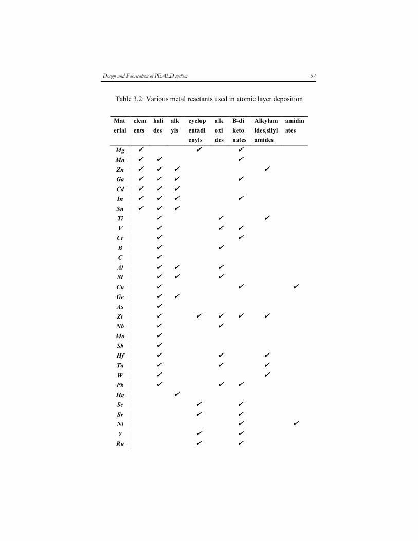
The precursors used in ALD can be divided in two main groups:
inorganic and metalorganic. Metalorganic reactants can further be classified
in to those containing a direct metal–carbon bond, that is, organometallic
reactants [9,18] and those containing no direct metal–carbon bond.
Typically, for inorganic reactants, elements and halides have been used; for
organometallic reactants, alkyls and cyclopentadienyls have been used. For
other metalorganic reactants, alkoxides, diketonates, amides, and amidinates
have been used in ALD experiments. Table 3.2 summarizes which types of
reactants have been used for which elements and it is clear that a wide range
of precursors are available for almost all metals and nonmetals [9-15].
Design and Fabrication of PEALD system 57
Table 3.2: Various metal reactants used in atomic layer deposition
Mat
erial
elem
ents
hali
des
alk
yls
cyclop
entadi
enyls
alk
oxi
des
Β-di
keto
nates
Alkylam
ides,silyl
amides
amidin
ates
Mg ���� ���� ����
Mn ���� ���� ����
Zn ���� ���� ���� ����
Ga ���� ���� ���� ����
Cd ���� ���� ����
In ���� ���� ���� ����
Sn ���� ���� ����
Ti ���� ���� ����
V ���� ���� ����
Cr ���� ����
B ���� ����
C ����
Al ���� ���� ����
Si ���� ���� ����
Cu ���� ���� ����
Ge ���� ����
As ����
Zr ���� ���� ���� ���� ����
Nb ���� ����
Mo ����
Sb ����
Hf ���� ���� ����
Ta ���� ���� ����
W ���� ����
Pb ���� ���� ����
Hg ����
Sc ���� ����
Sr ���� ����
Ni ���� ����
Y ���� ����
Ru ���� ����
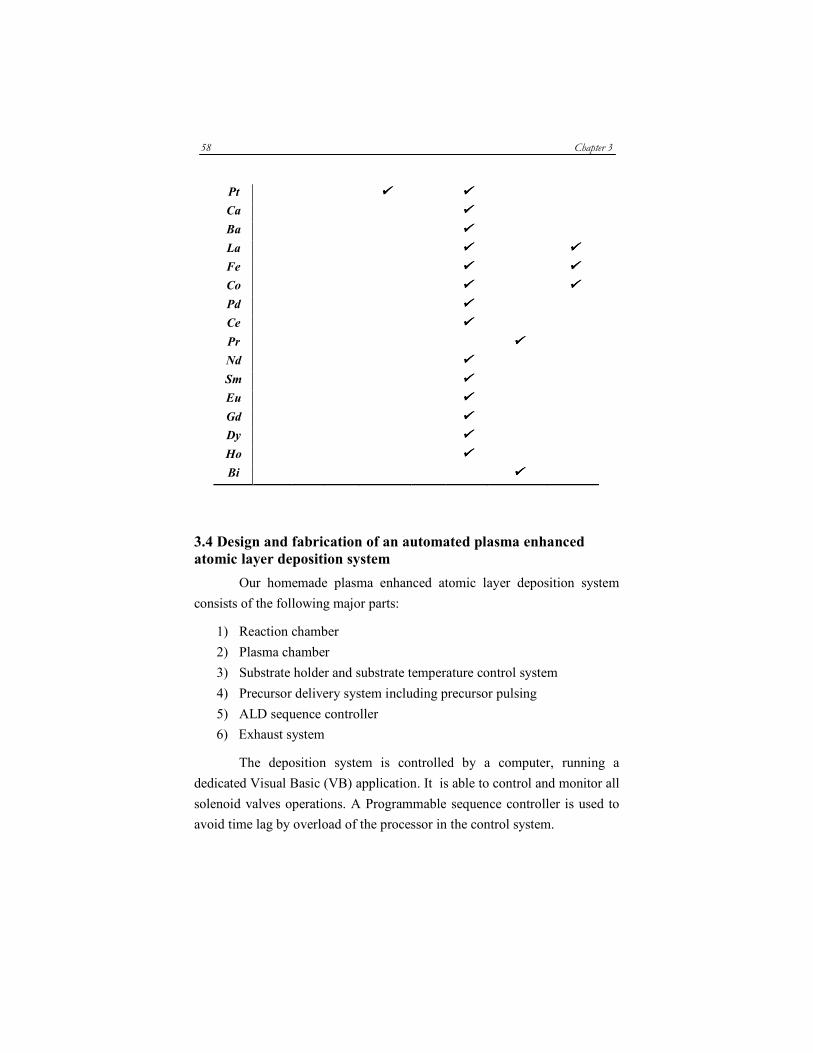
58 Chapter 3
Pt ���� ����
Ca ����
Ba ����
La ���� ����
Fe ���� ����
Co ���� ����
Pd ����
Ce ����
Pr ����
Nd ����
Sm ����
Eu ����
Gd ����
Dy ����
Ho ����
Bi ����
3.4 Design and fabrication of an automated plasma enhanced
atomic layer deposition system
Our homemade plasma enhanced atomic layer deposition system
consists of the following major parts:
1) Reaction chamber
2) Plasma chamber
3) Substrate holder and substrate temperature control system
4) Precursor delivery system including precursor pulsing
5) ALD sequence controller
6) Exhaust system
The deposition system is controlled by a computer, running a
dedicated Visual Basic (VB) application. It is able to control and monitor all
solenoid valves operations. A Programmable sequence controller is used to
avoid time lag by overload of the processor in the control system.

Design and Fabrication of PEALD system 59
3.4.1 ALD reaction chamber
ALD processes can be performed in different types of reactors over
a wide pressure range from atmospheric to ultrahigh vacuum. The reactor
type can be divided into two groups: inert gas flow reactors operating under
viscous flow conditions at pressures higher than or equal to 0.13mbar, and
high or ultrahigh vacuum reactors operating under molecular flow
conditions. From the viewpoint of cost effectiveness of the process, flow
reactors operating under viscous flow are more popular. This is primarily
due to (1) purging of a properly designed flow reactor is much more rapid
than evacuation of a high vacuum chamber, thus reducing the process time,
and (2) operating a UHV system is significantly costlier and challenging
than low vacuum systems. Our system is capable of working both in purging
as well as evacuation mode. Considering the cost and ease of maintenance
we have chosen viscous flow mode for most of our studies.
It is important to note that the reactor wall can be hot or cold type.
Hot wall reactors maintain the entire reactor at or near the deposition
temperature. The primary advantage of hot wall reactors is that, there is no
chance for precursor condensation on the wall and for secondary reactions is
not possible. But in cold wall chamber the chance for precursor condensation
is high and secondary reaction may occur, which leads to the formation of
particles on the cold surface. Our chamber is basically cold wall type and the
entire chamber can be divided as two zones hot and cold. Temperature of hot
zone can be produced by a heater which is resistively heated and vary from
room temperature to 5000C. Substrate holder is placed on the surface of
heater. Outer wall of the chamber is water cooled which create a temperature
gradient region referred to as cold zone. Temperature of this cold wall can
vary from room temperature to 1500C.
The system comprises of a cross flow type, cylindrical deposition
chamber made of corrosion resistant Stainless Steel 316L. Volume of the
chamber is approximately three litres. The chamber walls are water cooled.
Several feed through are attached to the walls of the chamber for gas inlet,
vacuum gauges, thermo couple, ac and dc high voltage provision, Langmuir

60 Chapter 3
probe etc. Figure 3.2 shows a detailed schematic illustration of ALD reaction
chamber.
Using this ALD system we had successfully grown thin films of
aluminum oxide in the hot zone. We have observed simultaneous formation
of alumina nano particles in cold zone during some of the trials. As recently
nano sized particles have attracted much attention since they play crucial
roles in certain advanced technologies, we have carried out a detailed
characterization of these alumina particles. The detailed theory and growth
mechanisms involved in both film and particles formation at each zone will
be explained in chapter 7 in terms of TMA and H2O reaction. The capability
of dual nature of this system to produce films and particles is again
confirmed by producing ZrO2 film and powder using zirconium-tert-
butoxide and water.
Figure 3.7: Schematic diagram of ALD reaction chamber (1-heater, 2-Top
electrode for DC plasma, 3-view port, 4-needle valve, 5-air inlet, 6- thermo
couple,7-To pump, 8-Substrate holder .
7
1
2
3
4
5
6
8
Design and Fabrication of PEALD system 61
The bottom of the reactor chamber is connected to a throttle valve
and diffusion pump (DP). The DP is connected to a backing pump. The top
of the chamber is closed by a large plane stainless steel (SS) lid with an o-
ring seal during thermal ALD.
3.4.2 Plasma chamber
In most ALD process the precursors used are usually metalorganics
which results in porosity, low density and high impury contaminated films
[19].These problems can be minimized by applying plasma. But, the
damages of plasma on the substrate and thin films should be carefully
considered. Therefore, much effort has been devoted to understand the
damage mechanisms and to find ways to avoid these damages in plasma
enhanced processes.
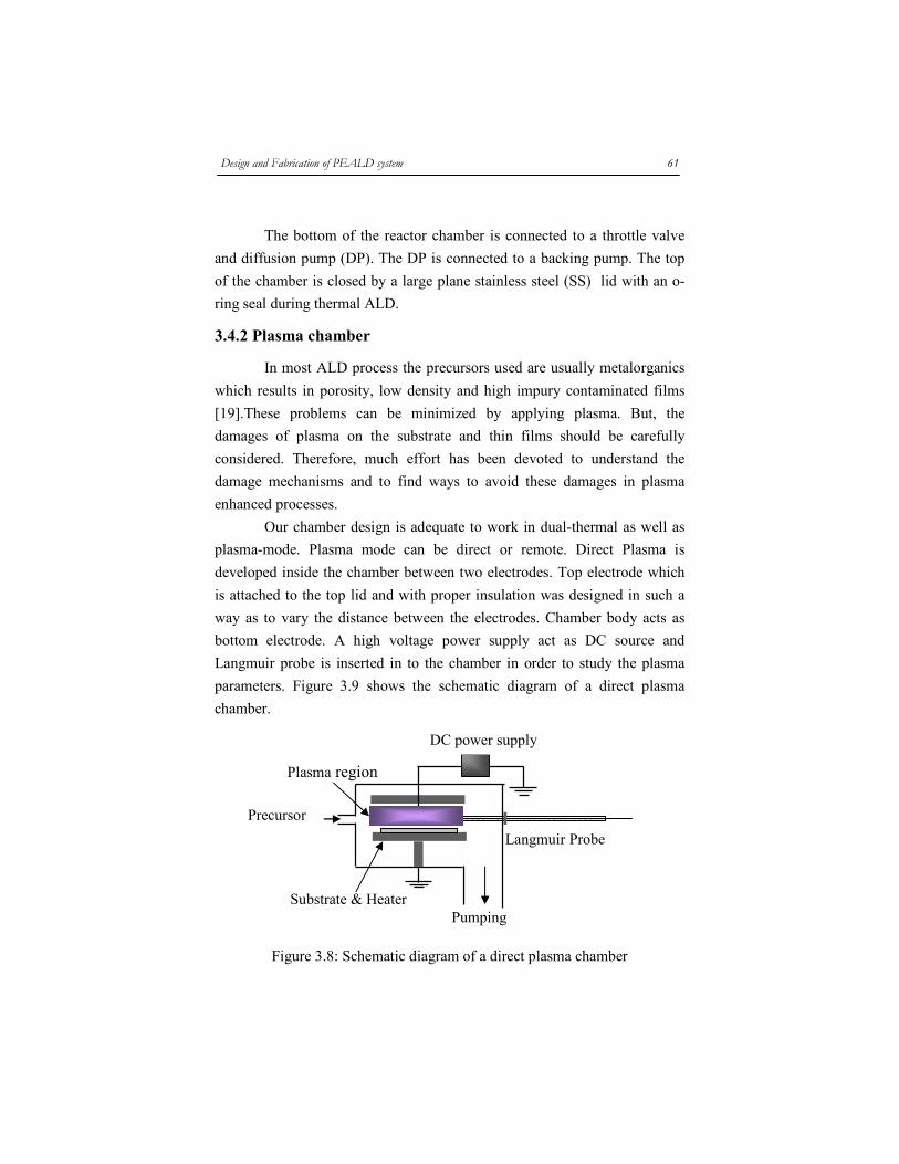
Our chamber design is adequate to work in dual-thermal as well as
plasma-mode. Plasma mode can be direct or remote. Direct Plasma is
developed inside the chamber between two electrodes. Top electrode which
is attached to the top lid and with proper insulation was designed in such a
way as to vary the distance between the electrodes. Chamber body acts as
bottom electrode. A high voltage power supply act as DC source and
Langmuir probe is inserted in to the chamber in order to study the plasma
parameters. Figure 3.9 shows the schematic diagram of a direct plasma
chamber.
Figure 3.8: Schematic diagram of a direct plasma chamber
Langmuir Probe
Precursor
DC power supply
Substrate & Heater Pumping
Plasma region

62 Chapter 3
With direct plasma assisted deposition also carbon content and the presence
of pores in the film resulting from direct exposure to the plasma were
noticed to some extent. It was observed that these can be further minimised
with the use of remote plasma.
Design of remote plasma chamber
Basic schematic of the remote plasma chamber and different
components with suitable material which can withstand temperature and low
pressure of the setup used are shown in Figure 3.9. Here a glass tube that
can sustain medium temperature and low pressure is used for the plasma
region of the chamber. This tube can be replaced by quartz tube at later
stages if required. In order to produce plasma, DC voltage was applied
between the electrodes, placed inside the tube. Various precautions and
safety features were included to make sure that no spark-discharge or any
other unwanted incidents happen during the operation of the reactor. Special
concern was given for maintaining proper distances between the electrodes
and grounded parts and keeping the electrodes clean.
Plasma was confined within a small region between the electrodes
within the glass tube and plasma properties could be changed either by
changing the spacing between the electrodes or by changing the voltage.
Positively charged active chemical species in the plasma are attracted
towards the substrate by biasing the substrate negatively. Even though some
electrons move towards the substrate they generally die out soon after they
come out of the plasma region by various recombination or capture
mechanisms. This is a condition which is desired, since electrons with high
kinetic energy moving towards the substrate may cause damages to the film
and also may cause non-conformal coating. Since slow positive particles
possess lesser kinetic energy than electrons they will neither cause film
damage nor arise in the temperature of the substrate. This condition is
suitable for a polymer or plastic type substrate to withstand.
The magnitude of negative potential applied to the substrate holder
is responsible for the speed and thus kinetic energy with which positive
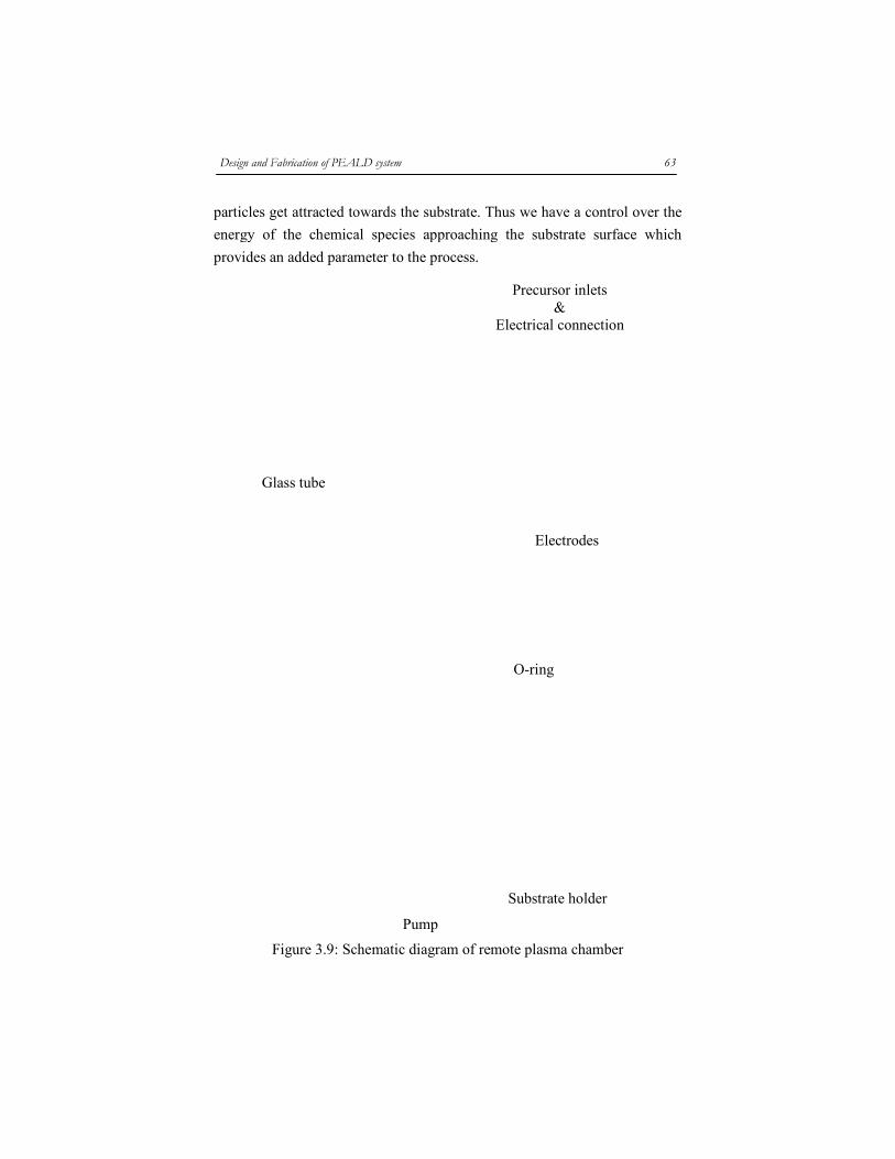
Design and Fabrication of PEALD system
particles get attracted towards the
energy of the chemical species approaching the substrate surface which
provides an added parameter to the process.
Figure 3.9: Schematic diagram of remote plasma chamber
Glass tube
Design and Fabrication of PEALD system 63
towards the substrate. Thus we have a control over th
energy of the chemical species approaching the substrate surface which
provides an added parameter to the process.
Figure 3.9: Schematic diagram of remote plasma chamber
Precursor inlets &
Electrical connection
Pump
Substrate holder
O-ring
Electrodes
63
Thus we have a control over the
energy of the chemical species approaching the substrate surface which

64 Chapter 3
Development of remote plasma
Plasma is a state of matter in which a certain portion of the particles
are ionized. In this experiment we use DC plasma as the ion source. The
plasma is generated by applying a HVDC supply 5kV between two
electrodes. Figure 3.9 shows the DC plasma arrangement. Plasma properties
are dependent upon the distance between electrodes, applied potential,
chamber pressure and type of gas inside the chamber. A Langmuir probe was
attached to the chamber for studying plasma characteristics. Figure 3.10
shows photographs of plasma source with nitrogen and argon at a pressure of
0.1mbar.
Figure 3.10: Photographs of the plasma source with nitrogen and argon
plasma
3.4.3 Precursor delivery system and precursor pulsing mechanism
Since ALD relies on a reaction sequence which reaches surface
saturation at each step, the design of precursor delivery systems for ALD
reactors is simpler than that of CVD systems where precise control of
precursor delivery to maintain a uniform flux is required. ALD is said to be
‘self-limiting’. That is, ALD ‘half-reactions’ proceed until the available

Design and Fabrication of PEALD system 65
reaction sites are used up, after which no more precursors react. In this way,
the surface catalysis aspect of ALD ensures the deposited layer is absolutely
uniform in thickness. ALD achieves conformal deposition on high aspect
ratio features because surface reaction sites are an ingredient of the reaction,
and are consumed by the reaction. Therefore uniform homogeneous
concentrations of precursors are not necessary in the reaction space to
achieve conformal deposition. It is merely necessary to provide enough of
each precursor to consume substantially at all available surface sites.
Variations of ALD processes may involve multiple precursors and
may use any number of chemical pathways. Oxidation pathways, using an
alkylamino metal precursor and an oxidizing agent, are popular for
depositing oxide layers. Reduction pathways, using a metal halide precursor
and a reducing agent, are also popular for depositing metal layers. Layers of
mixed chemistry, such as nitrides, oxynitrides, and the like, may also be
deposited by using two or more chemical precursors sequentially pulsed into
the reaction chamber. Other variations on the process itself feature pumping
out the reaction chamber to high vacuum between pulses, or continuously
purging the reaction chamber with a non-reactive gas while pulsing reactants
through the reaction space.
ALD processes are to be carefully managed. It is desired that
precursors react on the surface of the substrate, not in the space above the
substrate, to achieve a self-limiting surface reaction. Thus, one precursor
must be completely removed from the chamber before another precursor is
pulsed into the chamber. Trace amounts of precursors lingering in feed lines
and sides of the chamber react to produce compounds that deposit on
chamber and piping walls, potentially resulting in contamination of the
substrate surface with impurities or imperfections. Some precursors have
affinity for chamber materials, making it difficult and time consuming to
evacuate them from the chamber. Moisture or oxygen impurities in any
materials used as precursors or purge gases are particularly undesirable in an
ALD process. Complicating the task of managing these challenges is the fact
that process features such as valves and seals leak, and the smallest leaks in

66 Chapter 3
an ALD process can seriously degrade the results obtained. Therefore ALD
process and delivery system should be capable to manage these challenges.
For liquid precursors, there are two options:(i) delivery via carrier gas and
(ii) delivery via precursor volatilization. The system that we have developed
has capability of both type of precursor delivery.
Carrier gas assisted liquid precursor delivery is accomplished with
the help of a bubbler. A bubbler works by bubbling a high purity carrier gas
(Argon/Nitrogen) at a pressure lower than atmospheric pressure through a
volatile liquid precursor. The precursor vapour is carried by nitrogen gas
flow into deposition chamber. Since the carrier gas pressure is higher than
the chamber exhaust, the pressure gradient is sufficient to cause the gas
mixture to flow into the reactor. Under conditions where the precursor’s
equilibrium vapour pressure is maintained, the mass flow of precursor into
the reactor is proportional to the nitrogen carrier gas flow rate and the
precursor vapour pressure. Bubblers are best used for volatile liquid
precursors. Consistent and reproducible precursor delivery ultimately
depends on the bubbler design and on the vaporization kinetics of the
precursors. Low volatility liquid precursors can be delivered with a bubbler,
but reproducibility tends to be poor. If precursor heating is used to increase
the vapour pressure, care must be taken to avoid precursor decomposition in
the bubbler and to prevent downstream condensation of the precursors prior
to the deposition chamber.
In the present experiments both TMA and H2O have sufficient vapor
pressure (13 mbar and 31mbar respectively) at room temperature and the
operating chamber pressure vary from 0.12 mbar- 0.48 mbar. Thus,
adopting option (ii) was a natural choice, since precursors can be easily
introduced into the reaction chamber via pressure differential driven flow. In
addition, each precursor was separated by a purge. In the case of chemicals
with low vapour pressure the source was heated to a temperature below its
boiling point which will generate an increased vapor pressure. In addition,
all the flow lines carrying precursors were heated to higher temperature to
avoid vapour condensation.

Design and Fabrication of PEALD system 67
Figure 3.11: Schematic diagram of a bubbler.
Figure 3.12: Delivery part of ALD system (1-Solenoid valve, 2-needle valve,
3-bubbler, 4-mass flow meter, and 5.chamber inlet)
Figure 3.12 shows the schematic diagram of precursor delivery part
which consist of solenoid valves (Avcon), bubblers (SS316), mass flow

68 Chapter 3
meters (BRONKHORST) and needle valves. The entire precursor lines were
evacuated. Under this reduced pressure, precursor vapour were pulsed in to
reaction chamber by means of solenoid valves. Alternate pulsing of
precursors was achieved using solenoid valves which have response time
<100ms installed between the precursor source and the reaction chamber.
Solenoid valve operation was controlled by a sequential controller using a
visual basic (VB) program. The flow rate of the inert gas was measured by
mass flow meters. Needle valves were used for fine control of the flow rates
of carrier gas.
3.4.4 ALD sequence controller
The sequence controller is built around an 8-bit microcontroller
AT89C2051 with a PC interface through a serial port. A user friendly
interface written in Visual Basic is used to provided input data for defining
the sequences, various timings, number of cycles etc. An interrupt based
timing subroutine running in the microcontroller enables accurate control of
valve timings in unit of 10 milliseconds. The user interface also provides
visual indication of the sequences in real time.
Figure 3.13: User friendly interface for controlling ALD cycles

Design and Fabrication of PEALD system 69
Figure 3.14: Circuit diagram of hardware part of ALD sequential controller

70 Chapter 3
Figure 3.14: Circuit diagram of hardware part of ALD sequential controller

Design and Fabrication of PEALD system 71
Figu
re 3
.15
: Pho
togr
aph
of th
erm
al A
tom
ic L
ayer
Dep
osit
ion

72 Chapter 3
Figure 3.16: Photographs of Plasma Enhanced Atomic Layer Deposition
facility.
3.4.5 Exhaust system
A vacuum pumping system consisting of a 12M3/h rotary pump and
a 4 inch diffusion pump that can achieve an ultimate vacuum of 1x 10⁻⁵ mbar
is used to evacuate the ALD chamber. A penning gauge is used to measure
high vacuum in the chamber and two pirani gauges are used to measure
rotary vacuum at different points in the system. A liquid nitrogen trap was
placed between the chamber and vacuum pump. The pumping system has
provision to choose a high or low vacuum for a specific deposition. Most of
our depositions were conducted in low vacuum.

Design and Fabrication of PEALD system 73
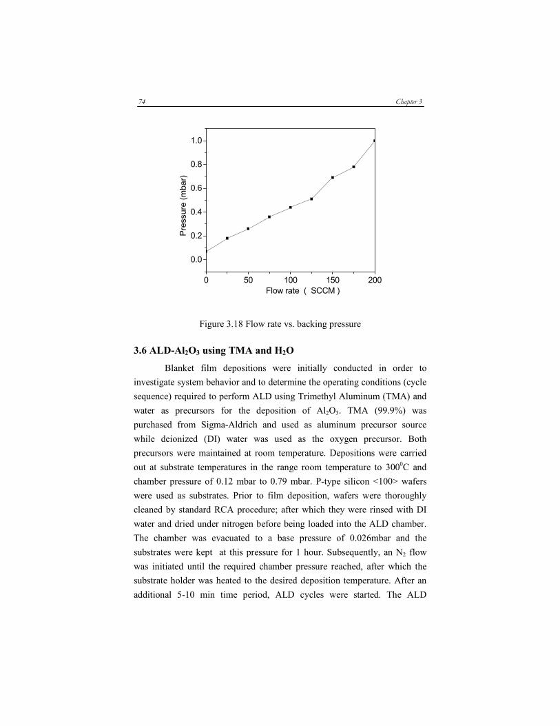
3.5 Optimisation of system parameters
To summarize our efforts in the area of design and fabrication of
automated plasma enhanced atomic layer deposition system the gas flow in
the chamber is plotted against time. Observations indicate that a reactor
configuration that offers proper provisions for purging the reactants after
each precursor exposure is the most critical aspect in the successful design of
ALD reactors.
By adjusting needle valves, the flow rates can be set at different
values up to 1000 SCCM. The flow rates of purge gas and each precursor
line at 200 SCCM, 400 SCCM, and 500 SCCM are plotted against the time.
This is shown in figure: 3.17. From the graph it can be understood that
within 15 seconds the gas flow attains a steady state in all investigated flow
ranges. The cycle times used in most of the alumina experiments were
around 35 seconds. This shows that the system attains a steady state within
one cycle of operation itself (which was later proved to be < 0.12nm
thickness of alumina film) which is a good indication of the quality of the
machine.
0 50 100 150 200
300
400
500
600
Flow
rat
e(sc
cm)
Time(sec)
mfc1
mfc2
purge
mfc1
purge
mfc2
mfc1
mfc2
purge
Figure 3.17: Time vs. Flow rates graph
74 Chapter 3
0 50 100 150 200
0.0
0.2
0.4
0.6
0.8
1.0
Flow rate ( SCCM )
Pre
ssure
(m
ba
r)
Figure 3.18 Flow rate vs. backing pressure
3.6 ALD-Al2O3 using TMA and H2O
Blanket film depositions were initially conducted in order to
investigate system behavior and to determine the operating conditions (cycle
sequence) required to perform ALD using Trimethyl Aluminum (TMA) and
water as precursors for the deposition of Al2O3. TMA (99.9%) was
purchased from Sigma-Aldrich and used as aluminum precursor source
while deionized (DI) water was used as the oxygen precursor. Both
precursors were maintained at room temperature. Depositions were carried
out at substrate temperatures in the range room temperature to 3000C and
chamber pressure of 0.12 mbar to 0.79 mbar. P-type silicon <100> wafers
were used as substrates. Prior to film deposition, wafers were thoroughly
cleaned by standard RCA procedure; after which they were rinsed with DI
water and dried under nitrogen before being loaded into the ALD chamber.
The chamber was evacuated to a base pressure of 0.026mbar and the
substrates were kept at this pressure for 1 hour. Subsequently, an N2 flow
was initiated until the required chamber pressure reached, after which the
substrate holder was heated to the desired deposition temperature. After an
additional 5-10 min time period, ALD cycles were started. The ALD

Design and Fabrication of PEALD system 75
deposition cycle consisted of: (1) TMA pulse, (2) N2 purge, (3) H2O pulse,
and (4) N2 purge. Details of the deposition conditions are explained in
chapter 5.
Successful layer by layer ALD process with sufficient exposure and
purge time and full saturation of the surface, should in principle result in
extremely uniform layers. Non uniformity of the deposited layers can occur
in initials cycles. Insufficient purge steps results vapour phase reaction
between precursors and results increased CVD like growth rate. Limited and
excess amount of precursors may also cause distinct growth rate than
expected. However not all uniformity problems are caused by critical
process parameters. The major advantage of ALD compared to CVD is its
non-critical nature of process parameters.
Thickness uniformity is one of the characteristic features of ALD. In
order to confirm this uniformity we measured the thickness of Al2O3 samples
prepared in our system at different location using an ellipsometer. Figure
3.19 shows the 2D plot of thickness variation on Si substrate at an area
4cm2.
Figure 3.19: 2D plots showing thickness variation in nm over a wafer surface
of area of 2cm 2cm.
3.7 Conclusions
We successfully designed and fabricated a compact and inexpensive
automated Atomic Layer Deposition system for depositing ultra-thin films,

76 Chapter 3
which can be used in a wide variety of research and industrial applications.
Our system is capable to work as thermal ALD and as plasma enhanced
ALD. System capabilities were confirmed by depositing ultra thin Alumina
films using TMA and water. System parameters were optimized in order to
work in ALD mode.
References
1. S. J. Yun, K. H. Lee, J. Skarp, H.-R. Kim and K.-S. Nam, J. Vac. Sci.
Technol. A 15, 2993 (1997).
2. T. Suntola, Thin Solid Films 216, 84 (1992).
3. M. Ritala, H. Saloniemi, M. Leskela, T. Prohaska, G. Friedbacher and
M. Grasserbauer, Thin Solid Films 286, 54 (1996).
4. S. M George, A.W. Ott, J.W Klaus, J. Phys. Chem. 100, 13121
(1996).
5. Steven M. George, Chem. Rev. 110 (1), 111 (2010).
6. M. Ritala and M. Leskela, Nanotechnology 10, 19-24 (1999).
7. M. Leskela and M. Ritala, Thin Solid films 409, 138 (2002).
8. N. R. Rajopadhye, S. B. Dake and V. Bhoraskar, Thin Solid Films
142, 127 (1986).
9. Rikka L. Puurunen, J. Appl . Phys. 97, 121301 (2005).
10. Jaebum Kim et al. Material Chemistry and Physics 78, 733 (2003).
11. M D Groner et al. Thin Solid Films 413, 186-197 (2002).
12. Michel Houssa, Series in Materials Science and Engineering, High-
k Gate Dielectrics, IOP publishing Ltd (2004).
13. J. L. Van Hemmen et al, Journal of The Electrochemical Society
154, 7, G165 (2007).
14. Lux, C. Colombier and H. Altena, Thin Solid Films 138, 49 (1986).
15. Petri I. Ra¨isa¨nen, Mikko Ritala and Markku Leskela J. Mater.
Chem. 12, 1415 (2002).
16. T. M. Klein, D. Niu, W. S. Epling, W. Li, D. M. Maher, C. C.
Hobbs, R. I. Hedge, I. J. R. Baumvol and G. N. Parsons, Appl.
Phys. Lett. 25, 4001 (1999).
17. C. Anthony, J. Jones, J. mater. Chem. 14, 3101 (2004).
Design and Fabrication of PEALD system 77
18. A. Salzer et al. Pure Appl. Chem. 71, 1557 (1999).
19. H. Jeon, and Y. Won, Appl. Phys. Lett. 93, 124104 (2008).
20. Design and fabrication of automated plasma enhanced atomic layer
deposition system for the deposition of ultra thin dielectric films, in
NSI- 32 October 24-26, at Tiruchengode, Tamilnadu (2007).
21. Anu Philip, Johney Issac,K. Rajeev Kumar, Jl. of Instrum. Soc. of
India 40, 4, 311 (2010).