design and analysis of synchronous dc-dc converter
TRANSCRIPT

DESIGN AND ANALYSIS OF SYNCHRONOUS DC-DC CONVERTER
By
IMTIAZ ALI SHAIKH
FINAL PROJECT REPORT
Submitted to the Electrical & Electronics Engineering Programme
in Partial Fulfillment of the Requirements
for the Degree
Bachelor of Engineering (Hons)
(Electrical & Electronics Engineering)
Universiti Teknologi Petronas
Bandar Seri Iskandar
31750 Tronoh
Perak Darul Ridzuan
© Copyright 2008
by
Imtiaz Ali Shaikh, 2008
ii

Approved:
CERTIFICATION OF APPROVAL
DESIGN AND ANALYSIS OF SYNCHRONOUS DC-DC CONVERTER
by
Imtiaz Ali Shaikh
A project dissertation submitted to the
Electrical & Electronics Engineering Programme
Universiti Teknologi PETRONAS
in partial fulfilment of the requirement for the
Bachelor of Engineering (Hons)
(Electrical & Electronics Engineering)
Dr. K. S Rama Rao
Project Supervisor
UNIVERSITI TEKNOLOGI PETRONAS
TRONOH, PERAK
June 2008
l1l
CERTIFICATION OF ORIGINALITY
This is to certify that I am responsible for the work submitted in this project, that the
original work is my own except as specified in the references and acknowledgements,
and that the original work contained herein have not been undertaken or done by
unspecified sources or persons.
Imtiaz Ali Shaikh
IV

ABSTRACT
This report presents literature and detailed theory of the synchronous
converter. The objective of the project is to Design and analyze synchronous d. c. to
d.c. converter. Synchronous rectification could be found in two main circuit
topologies (i) Forward converters and (ii) flyback converter. The Flyback converter is
a d.c. to d.c. converter. The author analyzed both converter types and came up with
successful results. Synchronous Conversion is a growing concept; where the main
objective is to reduce down power losses during rectification of power. By using
synchronous rectifiers we manage to minimize the size of the power supplies used in
portable appliances like Laptops and Mobile phones.
In order to design and analyze the circuit some parameters are to be fixed like;
operating frequency as 300 KHz, primary voltage for transformer as 15 V de,
secondary voltage as 3.3 Vdc and the output current as 0.8A. Any Mobile Phone
charger is having the same parameters. The author can claim that this would not be
the conventional/normal Mobile Phone charger as Synchronous rectification concept
is used.
v

ACKNOWLEDGEMENTS
I would like to express my great attribute to those who guide and helped me in
order to achieve my Final Year project at successful end. My enormous gratitude goes
to my FYP supervisor Dr. K.S Rama Rao, without him it was not possible to achieve
it, Mr. Musa, Miss Y anti, Misses Hawa, and Mr. Y aseen. I am also thankful to those
who guide and assist me indirectly. It was really great learning and continuous
support from them. I really appreciate their effort they put in to, as to get results.
VI

TABLE OF CONTENTS
ABSTRACT ..................................................................................... v
ACKNOWLEDGEMENT .................................................................... vi
LIST OF TABLES ............................................................................. .ix
LIST OF FIGURES .............................................................................. x
LIST OF ABBREVIATIONS ............................................................... xi
CHAPTER 1 INTRODUCTION ............................................................................. 1
1.1 Advantages of d. c. to d. c. converter. ..................................... 2
1.2 Problem statement.. ........................................................ 3
1.3 Background of study ......................................................................... .4
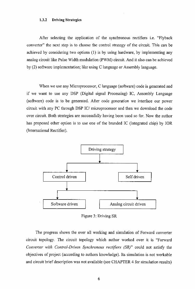
1.3.1 Application of Synchronous Rectifier (SR) .............................. 5 1.3 .2 Driving Strategies ............................................................ 6
1.4 Synchronous Rectification in Forward Converter. ..................... 7
1.4.1How Forward Converter Works ............................................ 8 1.5 Synchronous Rectification in Flyback Converter. ..................... 8
1.5.1 How SRs Work in Flyback Converter. .................................... 9
CHAPTER 2: LITERATURE REVIEW .................................................... .IO
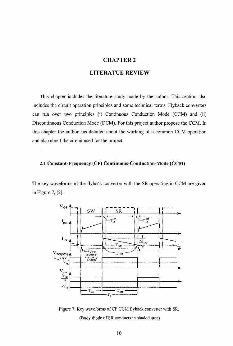
2.1 Constant-Frequency (CF) Continuous-Conduction-Mode (CCM).IO
2.2 CCM operation in Project Circuit ....................................... 12
2.2.1 Operation and analysis in Continuous Conduction Mode (CCM)
in Flyback ................................................................... 12
2.2.2 Tum On Phase ................................................................................. l3
2.2.3 CCM Tum OffPhase ...................................................... 14
CHAPTER3 METHODOLOGY ................................................................. l5
3.1 Design and verification ................................................. .l5
3.1.1 Research and Analysis .................................................... 19
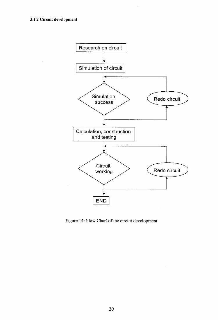
3.1.2 Circuit development.. .................................................... 20
CHAPTER 4 RESULTS AND DISCUSSION ................................................. 21
4.1 Forward Converter Simulation Results .............................. 21
4.2 Flyback Converter Simulation Results .............................. 23
CHAPTER 5 CONCLUSION ANDRECOMMENDATION ............................ 25
5.1 Conclusion ............................................................... 25
5.2 Recommendation ........................................................ 25
Vll

REFERENCES ................................................................................. 26
APPENDICES .................................................................................. 27
Appendix A Procedure to Select Circuit Components ............. 28
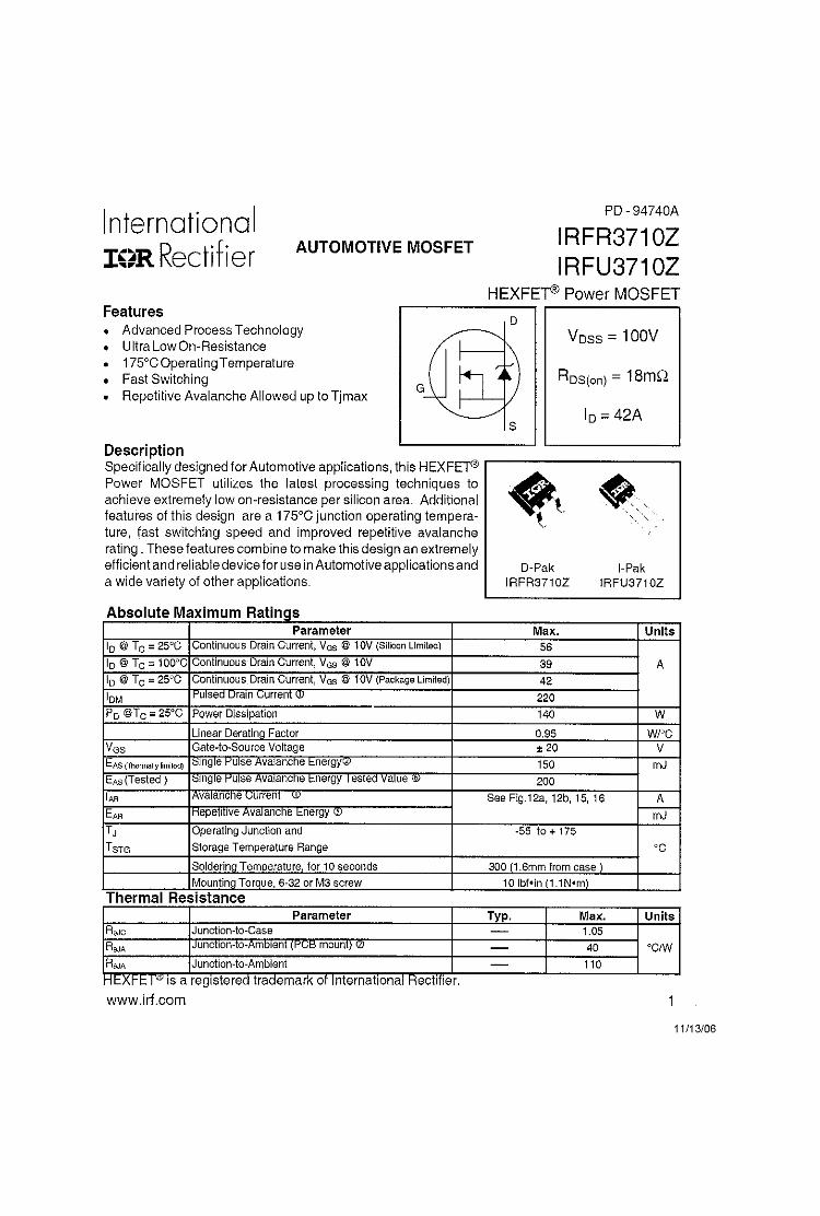
Appendix B MOSFET Datasheet... .................................... 31
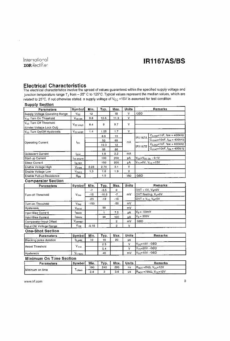
Appendix C IR1167S Datasheet. ....................................... 32
Vlll

LIST OF FIGURES
Figure 1: Forward-voltage comparison. . 2
Figure 2: Applications of SR. . . 5
Figure 3: Driving SR. . . 6
Figure 4: Forward converter with control driven SR.. . 7
Figure 5: Forward converter with control driven Sr. (After minor change). . . 7
Figure 6: Flyback Converter with SR Example. . 9
Figure 7: Key waveforms ofCF CCM flyback converter with SR. . 10
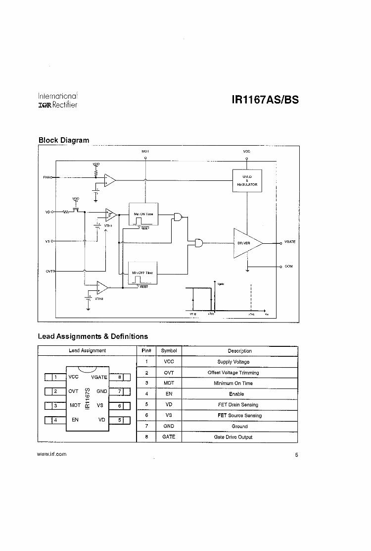
Figure 8: IR1167 SmartRectifier™ control IC. . 12
Figure 9: Secondary side CCM operation, MOT and Tblank. . 13
Figure 10: Primary and secondary currents and voltages for CCM. . 14
Figure 11: Flyback converter circuit topology. . 15
Figure 12: IR1167 Smart Rectifier control IC pin assignment. . 16
Figure 13: Flow chart of the Research and Analysis.. . 19
Figure 14: Flow Chart of the circuit development. . 20
Figure 15: Forward converter (After minor change. . 21
Figure 16 (a): Simulation Result for the Forward converter.. . 22
Figure 16 (b): Waveform for the Forward converter.. . 22
Figure 17: Flyback converter circuit topology. . 23
Figure 18 (a): Simulation Results for Flyback Converter. . 24
Figure 18 (b): Waveform for simulation. . 24
X

LIST OF ABBREVIATIONS
V ds (on)- Saturation Voltage, drain to source
Vgs -Gate Source Voltage
Vth- Threshold Voltage
Id - continuous drain current
Is - Continuous source current
Igss- Gate-to-source current
Rds (on)- Static drain-source ON-State resistance.
UTP- University Technology PETRONAS
CCM - Continuous Conduction Mode
DCM - Discontinuous Conduction Mode
XI