deposition of size-selected cu nanoparticles by inert gas ... · approach described in this paper...
TRANSCRIPT

NANO EXPRESS
Deposition of Size-Selected Cu Nanoparticles by Inert GasCondensation
M. Gracia-Pinilla • E. Martınez • G. Silva Vidaurri •
E. Perez-Tijerina
Received: 17 June 2009 / Accepted: 4 October 2009 / Published online: 6 November 2009
� to the authors 2009
Abstract Nanometer size-selected Cu clusters in the size
range of 1–5 nm have been produced by a plasma-gas-
condensation-type cluster deposition apparatus, which
combines a grow-discharge sputtering with an inert gas
condensation technique. With this method, by controlling
the experimental conditions, it was possible to produce
nanoparticles with a strict control in size. The structure and
size of Cu nanoparticles were determined by mass spec-
troscopy and confirmed by atomic force microscopy
(AFM) and scanning electron transmission microscopy
(STEM) measurements. In order to preserve the structural
and morphological properties, the energy of cluster impact
was controlled; the energy of acceleration of the nanopar-
ticles was in near values at 0.1 ev/atom for being in soft
landing regime. From SEM measurements developed in
STEM-HAADF mode, we found that nanoparticles are
near sized to those values fixed experimentally also
confirmed by AFM observations. The results are relevant,
since it demonstrates that proper optimization of operation
conditions can lead to desired cluster sizes as well as
desired cluster size distributions. It was also demonstrated
the efficiency of the method to obtain size-selected Cu
clusters films, as a random stacking of nanometer-size
crystallites assembly. The deposition of size-selected metal
clusters represents a novel method of preparing Cu nano-
structures, with high potential in optical and catalytic
applications.
Keywords Cu nanoparticles � Inert gas condensation �Cu cluster films � Structure of nanoscale materials
Introduction
Owing to their unique catalytic, electronic, magnetic, and
optical properties, different from their bulk species, nano-
particles continue to attract the attention of researchers [1].
Metal nanoparticles (NP’s) have been synthetically pro-
duced by different techniques for many years [2–8]. The
approach described in this paper is an inert gas condensation
(IGC) technique used before for synthesis of metal NP’s
[9–12]. The optical, electronic, and thermal properties of
metal NP’s endow them with potential application in elec-
trical and third-order nonlinear optical devices [13–18],
solid dielectric materials [19], nano-biomaterials [20], and
high thermal conductivity nanofluids [21]. Recently, atten-
tion has been focused on Cu nanoparticles due to their
optical and catalytic properties [22–25]. Particularly, the
optical and catalytic behavior in Cu nanoparticles is not well
understood. It is believed that absorption of light by metal
nanoparticles is dominated by the surface plasmon (SP)
resonance changing both the static and dynamic optical
M. Gracia-Pinilla � G. S. Vidaurri � E. Perez-Tijerina
Facultad de Ciencias Fısico-Matematicas, Universidad
Autonoma de Nuevo Leon, San Nicolas de los Garza,
Nuevo Leon 66450, Mexico
e-mail: [email protected]
E. Perez-Tijerina
e-mail: [email protected]
M. Gracia-Pinilla � G. S. Vidaurri � E. Perez-Tijerina
Centro de Innovacion, Investigacion y Desarrollo en Ingenierıa y
Tecnologıa, Laboratorio de Nanociencias y Nanotecnologıa
(CIIDIT-UANL), PIIT Monterrey, Apodaca, NL 66600, Mexico
E. Martınez (&)
Centro de Investigacion en Materiales Avanzados,
S.C.(CIMAV), Av. Alianza Norte #202, Parque de Investigacion
e Innovacion Tecnologica (PIIT), Nueva Carretera Aeropuerto
Km. 10, Apodaca, Nuevo Leon 66600, Mexico
e-mail: [email protected]
123
Nanoscale Res Lett (2010) 5:180–188
DOI 10.1007/s11671-009-9462-z
properties. These and other properties depend on their size,
size distribution, shape, and structure in addition to the
interaction between the surfaces of the nanoparticle. Control
of these features is not trivial as Cu nanoparticles formation
is extremely sensitive to reaction conditions [26, 27].
Although a variety of techniques for the production of Cu
nanoparticles have been developed, the main problem is still
the control of size that let us to explain the size effects on its
properties. In the present work, we describe the synthesis of
Cu nanoparticles using a grow-discharge sputtering with an
inert gas condensation (IGC) technique. The resulting
nanoparticles were analyzed by mass spectroscopy, scan-
ning transmission electron microscopy, and atomic force
microscopy. We present the results of the different experi-
mental analysis of the Cu NP’s and these results are dis-
cussed and contrasted for different experimental conditions.
Experimental
Copper NP’s were produced with a sputtering system
NanoSys 500, nanoparticles source from Mantis Deposition
Ltd. [28]. A schematic of the experimental set-up
employed in our laboratory for the production of size-
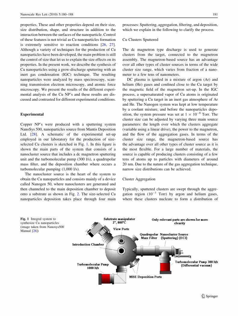
selected Cu clusters is sketched in Fig. 1. In this figure is
shown the main parts of the system that consists of a
nanocluster source that includes a dc magnetron sputtering
unit and the turbomolecular pump (300 l/s), a quadrupolar
mass filter, and the deposition chamber where occurs a
turbomolecular pumping (1,000 l/s).
The nanocluster source is the heart of the system to
obtain the Cu nanoparticles and consists mainly of a device
called Nanogen 50, where nanoclusters are generated and
then channeled to the main deposition chamber to deposit
onto a substrate as shown in Fig. 2. The size-selected Cu
nanoparticles deposition takes place through four main
processes: Sputtering, aggregation, filtering, and deposition,
which we explain in the following to clarify the process.
Cu Clusters Sputtered
The dc magnetron type discharge is used to generate
clusters from the target, connected to the magnetron
assembly. The magnetron-based source has an advantage
over all other types of cluster sources in terms of the wide
cluster size range, which varies from fraction of a nano-
meter to a few tens of nanometers.
DC plasma is ignited in a mixture of argon (Ar) and
helium (He) gases and confined close to the Cu target by
the magnetic field of the magnetron set-up. In the IGC
process, a supersaturated vapor of Cu atoms is originated
by sputtering a Cu target in an inert gas atmosphere of Ar
and He. The Nanogen system was kept at low temperature
by a coolant mixture, and before the nanoparticles depo-
sition, the system pressure was set at 1 9 10-8 Torr. The
cluster size can be adjusted by varying three main source
parameters: the length over which the clusters aggregate
(variable using a linear drive), the power to the magnetron,
and the flow of the aggregation gases. In terms of the
cluster size range, the magnetron-based source has
the advantage over all other types of cluster source as it is
the most flexible. For a large number of materials, the
source is capable of producing clusters consisting of a few
tens of atoms up to particles with diameters of around
20 nm. Due to the nature of the gas aggregation technique,
narrow size distributions can be achieved.
Cluster Aggregation
Typically, sputtered clusters are swept through the aggre-
gation region (10-1 Torr) by argon and helium gases,
where these clusters nucleate to form a distribution of
Fig. 1 Integral system to
synthesize Cu nanoparticles
(image taken from Nanosys500
Manual [28])
Nanoscale Res Lett (2010) 5:180–188 181
123
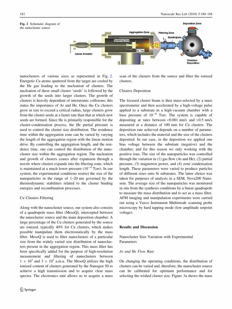
nanoclusters of various sizes as represented in Fig. 2.
Energetic Cu atoms sputtered from the target are cooled by
the He gas leading to the nucleation of clusters. The
nucleation of these small cluster ‘seeds’ is followed by the
growth of the seeds into larger clusters. The growth of
clusters is heavily dependent of interatomic collisions; this
states the importance of Ar and He. Once the Cu clusters
grow in size to exceed a critical radius, large clusters grow
from the cluster seeds at a faster rate than that at which new
seeds are formed. Since He is primarily responsible for the
cluster-condensation process, the He partial pressure is
used to control the cluster size distribution. The residence
time within the aggregation zone can be varied by varying
the length of the aggregation region with the linear motion
drive. By controlling the aggregation length, and the resi-
dence time, one can control the distribution of the nano-
cluster size within the aggregation region. The nucleation
and growth of clusters ceases after expansion through a
nozzle where clusters expands into the filtering zone, which
is maintained at a much lower pressure (10-4 Torr). In our
system, the experimental conditions restrict the size of the
nanoparticles in the range of 1–20 nm governed by the
thermodynamic stabilities related to the cluster binding
energies and recombination processes.
Cu Clusters Filtering
Along with the nanocluster source, our system also consists
of a quadrupole mass filter (MesoQ), intercepted between
the nanocluster source and the main deposition chamber. A
large percentage of the Cu clusters generated by the source
are ionized, typically 40% for Cu clusters, which makes
possible manipulate them electrostatically by the mass
filter. MesoQ is used to filter nanoclusters of a particular
size from the widely varied size distribution of nanoclus-
ters present in the aggregation region. This mass filter has
been specifically added for the purpose of high-resolution
measurement and filtering of nanoclusters between
1 9 103 and 3 9 107 a.m.u. The MesoQ utilizes the high
ionized content of clusters generated by the Nanogen 50 to
achieve a high transmission and to acquire clear mass
spectra. The electronics unit allows us to acquire a mass
scan of the clusters from the source and filter the ionized
clusters.
Clusters Deposition
The focused cluster beam is then mass-selected by a mass
spectrometer and then accelerated by a high-voltage pulse
applied to a substrate in a high-vacuum chamber with a
base pressure of 10-8 Torr. The system is capable of
depositing at rates between \0.001 nm/s and [0.5 nm/s
measured at a distance of 100 mm for Cu clusters. The
deposition rate achieved depends on a number of parame-
ters, which includes the material and the size of the clusters
deposited. In our case, in the deposition we applied one
bias voltage between the substrate (negative) and the
chamber, and for this reason we only working with the
positive ions. The size of the nanoparticles was controlled
through the variation in (1) gas flow (Ar and He), (2) partial
pressure, (3) magnetron power, and (4) zone condensation
length. These parameters were varied to produce particles
of different sizes onto Si substrates. The latter choice was
taken for purposes of analysis in a SEM, Nova200 Nano-
sem. The average size of the nanoparticles was monitored
in situ from the synthesis conditions by a linear quadrupole
to measure the mass distribution and to act as a mass filter.
AFM imaging and manipulation experiments were carried
out using a Veeco Instrument Multimode scanning probe
microscopy by hard tapping mode (low amplitude setpoint
voltage).
Results and Discussion
Nanocluster Size Variation with Experimental
Parameters
Ar and He Flow Rate
On changing the operating conditions, the distribution of
clusters can be varied and, therefore, the nanocluster source
can be calibrated for optimum performance and for
selecting the wished cluster size. Figure 3a shows the mass
Fig. 2 Schematic diagram of
the nanocluster source
182 Nanoscale Res Lett (2010) 5:180–188
123

spectrum of copper nanoparticles deposited on Si substrates
under 10, 30, 50, 70, and 90 sccm Ar flow rates where
deposition times were fixed for all deposition processes.
Nanoparticles of different sizes are clearly visible on the
mass spectrums. It is observed that the mean nanoparticle
size value of the distribution first increases with an increase
in the Ar flow rates to finally decrease for higher Ar flow
rates. Physically, the cluster growth phenomenon involves
several processes such as embryo formation through three
body collision, nucleation by cluster–cluster collision,
cluster growth via atomic condensation. Ar flow rate favors
the cluster growth because it favors a higher sputter rate
besides a better ionization and hence, more rapid cluster
formation. However, when a Ar flow rate reach some value
the mean cluster size decreases since Ar will also sweep the
cluster through the aggregation zone more rapidly, this
reducing the time for particle growth. The cluster growth
rate strongly depends on the collision probability between
clusters, and this collision probability can be increased by
increasing the time spent by a cluster within the growth
region. So, an increase in the gas flow rate of the carrier gas
and, hence, the drift velocity of the material within the
growth region decreases the time-of-flight of the clusters,
and the collision probability of the clusters also decreases.
Additionally, it was observed a clear dependence with He
from which a continuous decreasing in mean cluster size is
found with the increasing in He flow rate as shown in
Fig. 3b. The evident fall in intensity of the cluster beam at
higher He flow rate is probably due to the greater efficiency
of helium in sweeping the clusters out of the condensation
chamber. Higher He flow rates reduces the average particle
size by reducing the associated residence time in the
aggregation zone due to a higher drift velocity of the Cu
clusters within the growth region, similar to which occurs
with Ar for high flow rates.
Magnetron Power and Aggregation Length
The magnetron power was varied for a fixed aggregation
length, Ar and He flow rates, 25 and 2 sccm, respectively.
The resulting mass spectra are shown in Fig. 4a from
which we observe the strong dependence between mean
cluster mass and magnetron power for Cu nanoparticles
growth. It can be observed that Cu nanoparticle size has a
nearly linear relationship with the sputtering power of the
cluster source. The increasing in mean Cu cluster mass
with the increasing in magnetron power, it is explained in
terms of the higher ionization rate as a consequence of the
magnetron power supplied leading to a higher beam
intensity. Furthermore, Cu ions count with the aggregation
length was varied for fixed experimental parameters
(60.3 W, Ar: 25 sccm and He: 2 sccm). The results
obtained from mass spectra are shown in Fig. 4b. It is
observed that reducing the distance, i.e. aggregation length,
from the magnetron head to the first expansion aperture
reduces the distance and time whereby condensation can
occur so the average nanoparticle size is reduced. We have
found that from all the parameters influencing the nano-
particle size, the growth distance is the most determinant.
Increasing the growth distance increases the length of time;
the clusters have to grow before passing through the nozzle.
In the case of Cu nanoparticles, it is possible to move the
maximum from around 1 nm to 15 nm by increasing
the growth distance from 30 to 130 mm; larger sizes are
reached when the other experimental parameters are
changed. Copper clusters were detected with the minimum
growth distance, which could be explained by the small
nucleation barrier (DG/kT) for Cu clusters formation.
Clusters containing just one nanometer of diameter each
were easily produced.
Fig. 3 a Cu mass spectra profiles varying the Ar flow rate, b Relation
between mean cluster mass and He flow rate
Nanoscale Res Lett (2010) 5:180–188 183
123

Monodispersed Cu Nanoclusters: Structural
and Morphological Analysis
In order to preserve the structural and morphological
properties, the energy of cluster impact was controlled; the
energy of acceleration was close to 0.1 eV/atom. High
angle annular bright field image (HAADF)-STEM pictures
of 5 nm filtered Cu nanoparticles were acquired to obtain
the size distribution of the deposited nanoclusters onto
carbon coated grids as shown in Fig. 5a. In this figure is
possible to distinguish as dotted circles, nanoparticles with
5 nm as they were filtered through the MesoQ. Lower
magnification is also presented in Fig. 5b for a better
observation of dispersed nanoparticles as well to make size
measurements. Histogram in Fig. 5b let us to analyze the
mean size by measurements, which demonstrates a narrow
dispersion in cluster size filtered at 5 nm with a central
value in 5.5 nm, and the effectiveness of technique to
obtain nanoparticles of predetermined size. The size dis-
tributions indicate the good monodispersivity besides the
Fig. 4 a Cu mass spectra profiles varying the magnetron power and
b the aggregation length
Fig. 5 STEM-HAADF images of soft landed and monodispersed Cu
NPS filtered in 5 nm at different magnifications a 50 nm b 200 nm.
Histogram in 5 b shows the size distribution
184 Nanoscale Res Lett (2010) 5:180–188
123
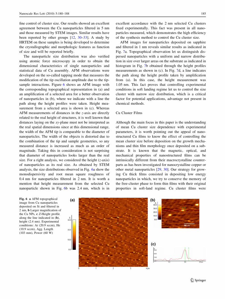
fine control of cluster size. Our results showed an excellent
agreement between the Cu nanoparticles filtered in 5 nm
and those measured by STEM images. Similar results have
been reported by other groups [12, 30–33]. A study by
HRTEM on these samples is being developed to determine
the crystallographic and morphologic features as function
of size and will be reported briefly.
The nanoparticle size distribution was also verified
using atomic force microscopy in order to obtain the
dimensional characteristics of single nanoparticles and
statistical data of Cu assembly. AFM observations were
developed on the so-called tapping mode that measures the
modification of the tip oscillation amplitude due to the tip-
sample interactions. Figure 6 shows an AFM image with
the corresponding topographical representation in (a) and
an amplification of a selected area for a better observation
of nanoparticles in (b), where we indicate with a line the
path along the height profiles were taken. Height mea-
surement from a selected area is shown in (c). Whereas
AFM measurements of distances in the z-axis are directly
related to the real height of structures, it is well known that
distances laying on the xy-plane must not be interpreted as
the real spatial dimensions since at this dimensional range,
the width of the AFM tip is comparable to the diameter of
nanoparticles. The width of the objects is distorted due to
the combination of the tip and sample geometries, so any
measured distance is increased as much as an order of
magnitude. Taking this in consideration is not surprising
that diameter of nanoparticles looks larger than the real
size. For a right analysis, we considered the height (z-axis)
of nanoparticles as its real size. As obtained by STEM
analysis, the size distributions observed in Fig. 6a show the
monodispersivity and root mean square roughness of
0.4 nm for nanoparticles filtered in 2 nm. It is worth a
mention that height measurement from the selected Cu
nanoparticle shown in Fig. 6b was 2.4 nm, which is in
excellent accordance with the 2 nm selected Cu clusters
fixed experimentally. This fact was present in all nano-
particles measured, which demonstrates the high efficiency
of the synthesis method to control the Cu cluster size.
AFM images for nanoparticles deposited on sapphire
and filtered in 1 nm reveals similar results as indicated in
Fig. 7a. Topographical observation let us distinguish dis-
persed nanoparticles with a uniform and narrow distribu-
tion in size over larger areas on the substrate as indicated in
histogram in Fig. 7b obtained through the height profiles
measurements as shown in (c). In Fig. 7d, a line indicates
the path along the height profile taken by amplification
from (a). In this case, the height measurement was
1.05 nm. This fact proves that controlling experimental
conditions in soft landing regime let us to control the size
cluster with narrow size distribution, which is a critical
factor for potential applications, advantage not present in
chemical methods.
Cu Cluster Films
Although the main focus in this paper is the understanding
of mean Cu cluster size dependence with experimental
parameters, it is worth pointing out the appeal of nano-
structured Cu films to know the effect of controlling the
mean cluster size before deposition on the growth mecha-
nisms and thin film morphology once deposited on a sub-
strate. It is known that the magnetic, optical, and
mechanical properties of nanostructured films can be
intrinsically different from their macrocrystalline counter-
parts as has been investigated for nanocrystalline copper or
other metal nanoparticles [29, 30]. Our strategy for grow-
ing Cu thick films consisted in depositing low energy
nanoparticles in which, we try to conserve the memory of
the free-cluster phase to form thin films with their original
properties in soft-land regime. Cu cluster films were
Fig. 6 a AFM topographical
image from Cu nanoparticles
deposited on Si and filtered in
2 nm, b Larger magnification of
the Cu NPs, c Z-Height profile
along the line indicated in (b),
height (2.4 nm). Experimental
conditions: Ar (20.9 sccm), He
(10.9 sccm), Agg. Length
(103 mm), Power (60 W)
Nanoscale Res Lett (2010) 5:180–188 185
123

deposited for one hour and filtered at 20 nm with the
experimental conditions as indicated in Fig. 8. From this,
we can observe that films are porous, since low-energy
clusters tend to pile up on the substrate, leaving large
cavities, which are desirable for retaining their high sur-
face/volume ratio. From AFM observations, in Fig. 8a, we
Fig. 7 a AFM topographical
image from Cu nanoparticles
deposited on sapphire and
filtered in 1 nm, b Particle size
histogram obtained from the
height of the NPs, c Z-Height
profile along the line indicated
in (d), d Larger magnification
from (a). Experimental
conditions: Ar (10 sccm), He
(25 sccm), Agg. Length
(30 mm), Power (62 W)
Fig. 8 a AFM topographical
image from a Cu nanosized thin
film deposited on Si and filtered
in 20 nm, b Particle size
histogram obtained from the
height of the NPs, c Larger
magnification of the film from
(a), d Z-Height profile along the
line indicated in (c), height
(19.1 nm). Experimental
conditions: Ar (25 sccm), He
(2.2 sccm), Agg. Length
(100 mm), Power (60 W)
186 Nanoscale Res Lett (2010) 5:180–188
123

note that the shape of nanoparticles is perfectly spherical
and sized as they were filtered. Since the kinetic energy is
negligible, compared to the bonding energy of an atom in
the cluster, no fragmentation of the cluster occurs upon
impact on the substrate. In this case, the height measure-
ment (z-axis) shown in Fig. 8b was 19.1 nm and as pre-
viously, it was considered as its real size obtained through
the height profiles, as shown in Fig. 8c and d. Statistical
analysis made through these measurements is summarized
in the histogram in (b). The Gaussian curve that fit to the
data is centered in 19.1 ± 0.9 nm; this value is slightly
deviated from the size predetermined experimentally but
still maintains the low dispersion in size as in the case of
monodispersed nanoparticles. The strict control of experi-
mental parameters by IGC technique leads to obtain size-
selected Cu clusters films, as a random stacking of nano-
meter-size crystallites assembly. Besides the importance of
control size as Cu cluster films, it is important to under-
stand how the size of these crystallites is determined and
how stable the nanostructured film is. We can anticipate
that the physical mechanism for cluster size evolution is, as
in the monodispersed case, sintering by atomic diffusion.
For thick films, however, surface diffusion can only be
effective before a given cluster has been ‘‘buried’’ by the
subsequent deposited Cu clusters. Thus, most of the size
evolution takes place during growth, for later the physical
routes to coalescence are expected to be much slower. For
Cu thick films, a reasonable assumption is that a cluster
impinging on a surface already covered by a layer of
clusters does not diffuse, because it forms strong bonds
with the layer of deposited Cu clusters. The process differs
from submonolayer growth in two main ways: first, an
impinging cluster has more than one neighbor; second,
clusters are not free to move. These conditions make the
Cu cluster film stable to the growing; hence, the size of the
crystallites is comparable to the size of the free clusters.
Low kinetics energy and contact angle are also crucial to
determine the spherical geometry formed on the substrate.
Clearly, further experimental and theoretical work is nee-
ded in order to confirm or invalidate our suggestions. Our
actual research is linked to a clear understanding of the
underlying mechanisms.
Summary
We have investigated the growth of Cu nanoparticles in a
plasma enhanced sputtering gas aggregation type growth
region. Various sputtering parameters were varied to
observe the change in the size distributions of the nano-
particles. It was found that Ar flow rate favors the cluster
growth but when this flow reach some critical value the
mean cluster size decreases since Ar also sweep the cluster
through the aggregation zone this reducing the time for
particle growth. A continuous decreasing in mean cluster
size was also observed with the increasing in He flow, which
reveals its effective role to reduce the size by reducing the
associated residence time in the aggregation zone. Cu
nanoparticle size is also controlled with the sputtering
power, a nearly linear relationship was found, however, the
most determinant experimental parameter to control size
seems to be the aggregation length. From STEM and AFM
measurements, we found that nanoparticles were monodi-
spersed with the selected size, this demonstrates the effi-
ciency of IGC technique to obtain cluster with the desired
size. Additionally, controlling experimental parameters by
IGC technique leads to obtain size-selected Cu cluster films.
The deposition of size-selected Cu clusters represents a
novel method of preparing Cu nanostructures, with high
potential in optical and catalytic applications.
Acknowledgments M. A. Gracia-Pinilla thank to PROMEP for
their support through grant PROMEP/103.5/09/3905. The authors
thank J. Sainz, J. Flores, and J. Aguilar for their technical help.
References
1. V.F. Puntes, K.M. Krishnan, A.P. Alivisatos, Science 291, 2115
(2001)
2. F.S. Diana, S.H. Lee, P.M. Petroff, E.J. Kramer, Nano Lett. 3,
891 (2003)
3. L. Qi, J. Ma, J. Shen, J Colloid Interf. Sci. 186(2), 498 (1997)
4. P. Chen, X. Wu, J. Lin, K.L. Tan, J. Phys. Chem. B 103(22), 4559
(1999)
5. N. Arul Dhas, C. Paul Raj, A. Gedanken, Chem. Mater. 10(5),
1446 (1998)
6. H.T. Zhu, C.Y. Zhang, Y.S. Yin, J Cryst. Growth 270, 722 (2004)
7. H. Ohde, F. Hunt, C.M. Wai, Chem.Mater. 13(11), 4130 (2001)
8. S.S. Joshi, S.F. Patil, V. Iyer, S. Mahumuni, Nanostruct. Mater.
10(7), 1135 (1998)
9. I.M. Goldby, B. Von Issendorff, L. Kuipers, R.E. Palmer, Rev.
Sci. Instrum. 68, 3327 (1997)
10. S. Yamamuro, K. Sumiyama, K. Suzuki, J. Appl. Phys. 85, 483
(1999)
11. T. Hihara, K. Sumiyama, J. Appl. Phys. 84, 5270 (1998)
12. E. Perez-Tijerina, M. Gracia Pinilla, S. Mejıa-Rosales, U. Ortiz-
Mendez, A. Torres, M. Jose-Yacaman, Faraday Discuss 138, 353
(2008)
13. M.L. Wu, D.H. Chen, T.C. Huang, Chem. Mater 13, 599 (2001)
14. N.R. Jana, Z.L. Wang, T.K. Sau, T. Pal, Curr. Sci. 19, 1367
(2002)
15. F. Kim, J.H. Song, P. Yang, J. Am. Chem. Soc. 124, 14316
(2002)
16. N.R. Jana, L. Gearheart, C.J. Murphy, Chem. Commun. 7, 617
(2001)
17. X. Liu, W. Cai, H. Bi, J. Mater. Res. 17, 1125 (2002)
18. C. Huang, C.Z. Yang, Appl. Phys. Lett. 74, 1692 (1999)
19. K. Akamatsu, S. Deki, J. Mater. Chem. 7, 1773 (1997)
20. M. Kogiso, K. Yoshida, K. Yase, T. Shimizu, Chem. Commun.
2492 (2002)
21. J.A. Eastman, S.U.S. Choi, S. Li, W. Yu, L. Thompson, J. Appl.
Phys. Lett. 78, 718 (2001)
22. M. Zhao, L. Sun, R. Crooks, J. Am. Chem. Soc. 120, 4877 (1998)
Nanoscale Res Lett (2010) 5:180–188 187
123

23. J.Y. Bigot, Phys. Rev. Lett. 75, 4702 (1995)
24. T.S. Ahmadi, J. Phys. Chem. 100, 8053 (1996)
25. M. Perner, Phys. Rev. Lett. 78, 2192 (1997)
26. J.H. Kim, T.A. Germer, G.W. Mulholland, S.H. Ehrman, Adv.
Mater. 14, 518 (2002)
27. H.C. Choi, Y.M. Jung, S.B. Kim, Intl. J. Nanosci. 1, 443 (2002)
28. Mantis Deposition Ltd. Oxford, England. www.mantisdeposition.
com
29. J. Schiotz, T. Rasmussen, K.W. Jacobsen, O.H. Nielsen, Philos.
Mag. Lett. 74, 339 (1996)
30. M.A. Gracia-Pinilla, D. Ferrer, S.J. Mejıa-Rosales, E. Perez-
Tijerina, Nanoscale Res. Lett. 4, 896 (2009)
31. Z.Y. Li, N.P. Young, M. Di Vece, R.E. Palmer, A.L. Bleloch,
B.C. Curley, N.P. Young, R.L. Johnston, J. Jiang, J. Yuan, Nature
451, 46 (2008)
32. B.C. Curley, R.L. Johnston, N.P. Young, Z.Y. Li, M. Di Vece,
R.E. Palmer, A.L. Bleloch, J. Phys. Chem. C 111, 17846 (2007)
33. R. Wang, O. Dmitrieva, M. Farle, G. Dumpich, M. Acet, S.
Mejia-Rosales, E. Perez-Tijerina, M.J. Yacaman, C. Kisielowski,
J. Phys. Chem. C 113, 4395 (2009)
188 Nanoscale Res Lett (2010) 5:180–188
123