dependence of the thickness and composition of the hfo2/si...
TRANSCRIPT
CINVESTAV 1
P.G. Mani-González and A. Herrera-Gomez
Dependence of the thickness and composition of the HfO2/Si interface layer on annealing
CINVESTAV-UNIDAD
QUERETARO
CINVESTAV 2
background
• Introduction – ALD
– DC Sputtering
– XPS
• ARXPS
• Growth of HfO2 films by ALD– Caracterization by XPS
• Growth of TaN films by DC sputtering– Caracterization by XPS
• Annealing of Si/HfO2/TaN– Removed TaN
– Charaterization by XPS
• Conclusions
CINVESTAV 3
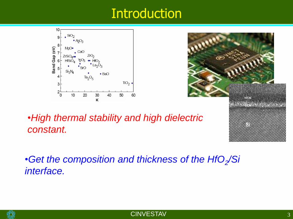
Introduction
•High thermal stability and high dielectric
constant.
•Get the composition and thickness of the HfO2/Si
interface.
CINVESTAV 4
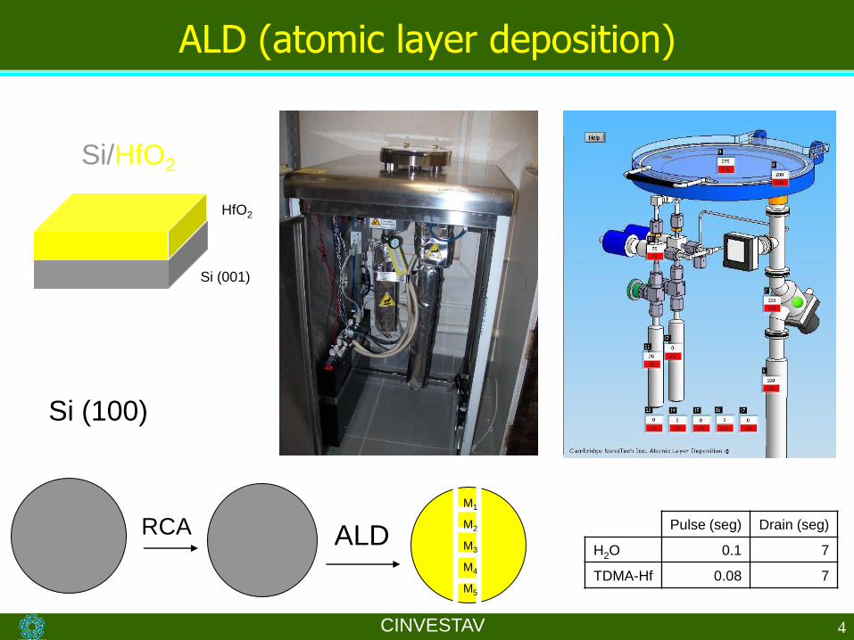
ALD (atomic layer deposition)
Si/HfO2
Si (001)
HfO2
RCA
Si (100)
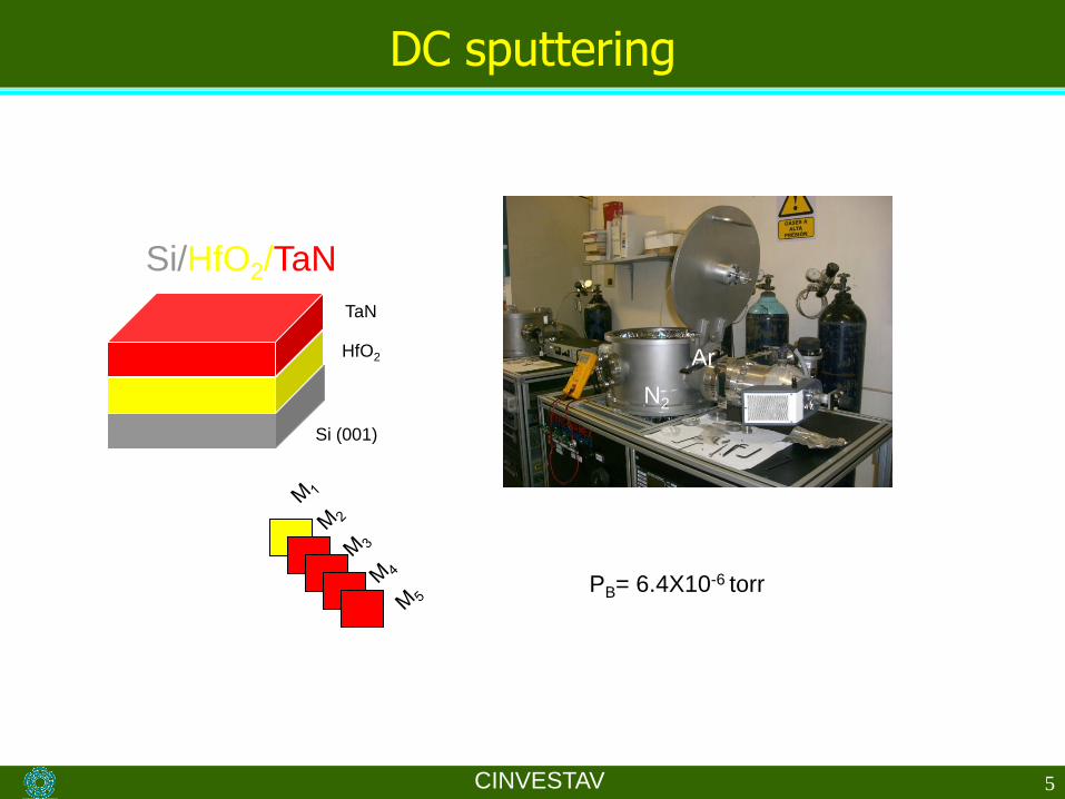
M1
M2
M3
M4
M5
ALDPulse (seg) Drain (seg)
H2O 0.1 7
TDMA-Hf 0.08 7
CINVESTAV 5
DC sputtering
Si/HfO2/TaN
Si (001)
TaN
HfO2
PB= 6.4X10⁻⁶ torr
Ar
N2
CINVESTAV 6
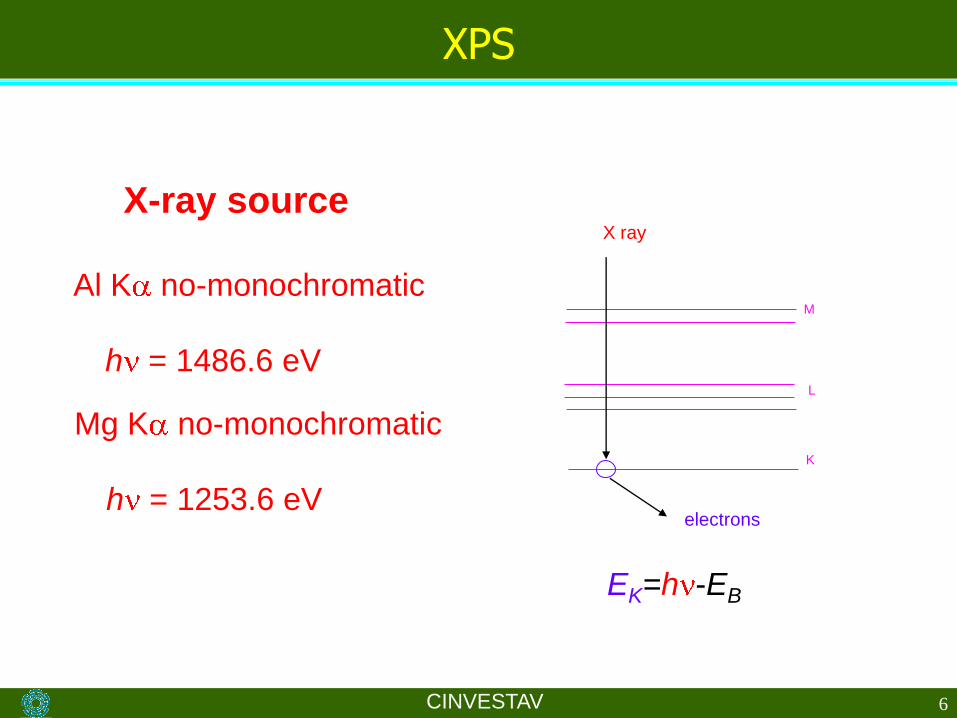
XPS
X-ray source
Al K no-monochromatic
h = 1486.6 eV
K
L
M
electrons
X ray
EK=h -EB
Mg K no-monochromatic
h = 1253.6 eV
CINVESTAV 7
1385 1390 1395 1400 1405 1410 1415 1420 1425
0
500
1000
1500
2000
2500
3000
Inte
nsity
Kinetic Energy
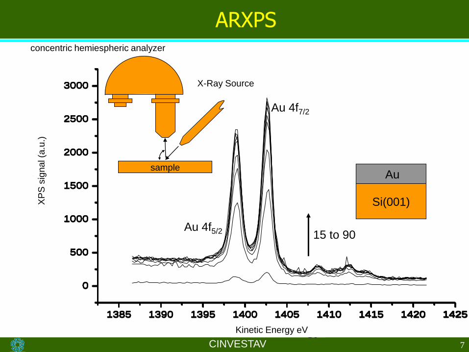
Au 4f7/2
1385 1390 1395 1400 1405 1410 1415 1420 1425
0
500
1000
1500
2000
2500
3000
Inte
nsity
Kinetic Energy
1385 1390 1395 1400 1405 1410 1415 1420 1425
0
500
1000
1500
2000
2500
3000
Inte
nsity
Kinetic Energy
1385 1390 1395 1400 1405 1410 1415 1420 1425
0
500
1000
1500
2000
2500
3000
Inte
nsity
Kinetic Energy
1385 1390 1395 1400 1405 1410 1415 1420 1425
0
500
1000
1500
2000
2500
3000
Inte
nsity
Kinetic Energy
1385 1390 1395 1400 1405 1410 1415 1420 1425
0
500
1000
1500
2000
2500
3000
Inte
nsity
Kinetic Energy
1385 1390 1395 1400 1405 1410 1415 1420 1425
0
500
1000
1500
2000
2500
3000
Inte
nsity
Kinetic Energy
1385 1390 1395 1400 1405 1410 1415 1420 1425
0
500
1000
1500
2000
2500
3000
Inte
nsity
Kinetic Energy
1385 1390 1395 1400 1405 1410 1415 1420 1425
0
500
1000
1500
2000
2500
3000
Inte
nsity
Kinetic Energy
sample
X-Ray Source
Au 4f5/2
ARXPSconcentric hemiespheric analyzer
Si(001)
Au
15 to 90
XP
S s
ign
al (a
.u.)
Kinetic Energy eV
CINVESTAV 8
background
• Introduction – ALD
– DC Sputtering
– XPS
• ARXPS
• Growth of HfO2 films by ALD– Caracterization by XPS
• Growth of TaN films by DC sputtering– Caracterization by XPS
• Annealing of Si/HfO2/TaN– Removed TaN
– Charaterization by XPS
• Conclusions
CINVESTAV 9
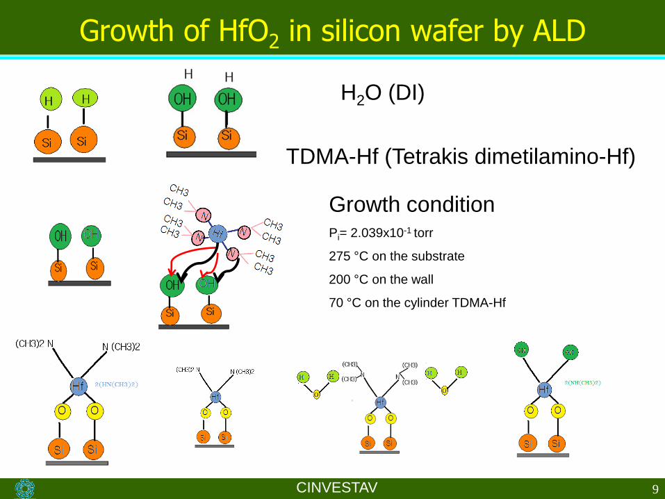
Growth of HfO2 in silicon wafer by ALD
TDMA-Hf (Tetrakis dimetilamino-Hf)
H2O (DI)
Growth conditionPi= 2.039x10⁻¹ torr
275 °C on the substrate
200 °C on the wall
70 °C on the cylinder TDMA-Hf

CINVESTAV 10
ARXPS in sample with 30 cycles
Si 2p
Hf 4f
O 1s
C 1s
Binding energy
Inte
nsity
CINVESTAV 11
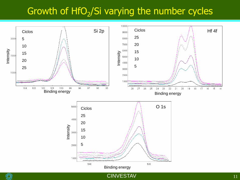
Growth of HfO2/Si varying the number cycles
Hf 4fSi 2p
O 1s
Ciclos
25
20
15
10
5
Ciclos
5
10
15
20
25
Ciclos
25
20
15
10
5
Binding energy
Inte
nsity
Binding energy
Inte
nsity
Binding energy
Inte
nsity
CINVESTAV 12
background
• Introduction – ALD
– DC Sputtering
– XPS
• ARXPS
• Growth of HfO2 films by ALD– Caracterization by XPS
• Growth of TaN films by DC sputtering– Caracterization by XPS
• Annealing of Si/HfO2/TaN– Removed TaN
– Charaterization by XPS
• Conclusions
CINVESTAV 13
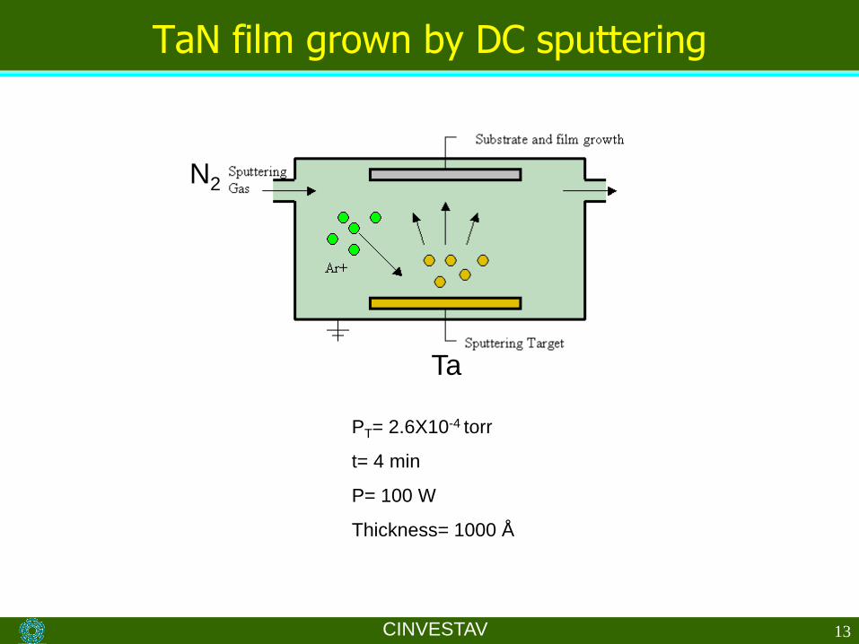
TaN film grown by DC sputtering
N2
Ta
PT= 2.6X10⁻⁴ torr
t= 4 min
P= 100 W
Thickness= 1000 Å

CINVESTAV 14
Characterization XPS in TaN films
Ta 4fTa 4d
N 2.5%
N 5%
N 10%
N 1s
Binding energy
Inte
nsity

CINVESTAV 15
Comparing TaN films grown by laser ablation and DC Sputtering
Ta 4f
Laser ablation *
10
5
2.5
N flow (%) Ar flow (%) N (cm3) Ar (cm3) Thickness (Å) Resistivity (Ω cm)
2.5 97.5 0.6 24.4 1464 1.596E+02
5 95 1.3 23.7 1090 7.358E-02
10 90 2.5 22.5 1087 6.36E-04
1000 3.73E-04 Laser A.
Binding energy
Inte
nsity
* Dr. Wencel de la Cruz (CNyN)
CINVESTAV 16
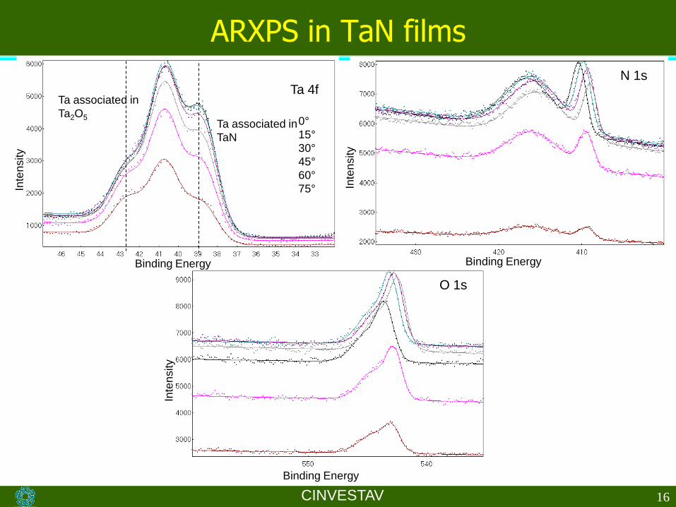
ARXPS in TaN films
N 1s
O 1s
Ta 4f
0°
15°
30°
45°
60°
75°
Binding Energy
Inte
nsity
Inte
nsity
Binding Energy
Inte
nsity
Binding Energy
Ta associated in
TaN
Ta associated in
Ta2O5
CINVESTAV 17
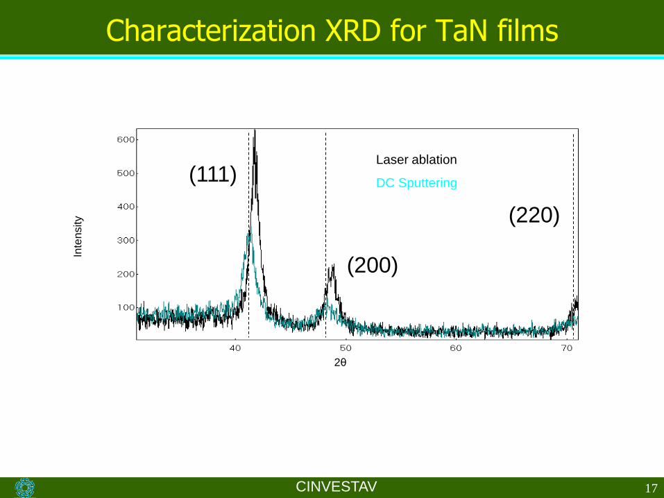
Characterization XRD for TaN films
(111)
(200)
(220)
2θ
Inte
nsity
Laser ablation
DC Sputtering

CINVESTAV 18
background
• Introduction – ALD
– DC Sputtering
– XPS
• ARXPS
• Growth of HfO2 films by ALD– Caracterization by XPS
• Growth of TaN films by DC sputtering– Caracterization by XPS
• Annealing of Si/HfO2/TaN– Removed TaN
– Charaterization by XPS
• Conclusions
CINVESTAV 19
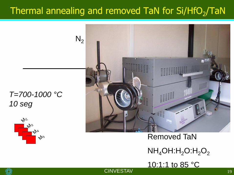
Thermal annealing and removed TaN for Si/HfO2/TaN
N2
T=700-1000 °C
10 seg
T2
AireAire
N2
Removed TaN
NH4OH:H2O:H2O2
10:1:1 to 85 °C

CINVESTAV 20
XPS after removed TaN filmO 1s
700 °C
800 °C
900 °C
1000 °C
Si 2pHf 4f
O associated
in HfO2
O associated
in SiO2
530.52 eV
531.92 eV
17.09 eV18.42 eV
99.4 eV
101.93 eV
399.17 eV405.14 eVN 1s
Ta 4f is not
NO2*
* V.B. Wiertz, P. Bertrand, Identification of the n-containing functionalities introduced at the surface of ammonia plasma treated carbon fibres by combined
TOF SIMS and XPS, Unité de Physico-Chimie et de Phys. Des Mat., Univ. Louvain 1348 Editor, Louvain.
Binding Energy
Inte
nsity
CINVESTAV 21
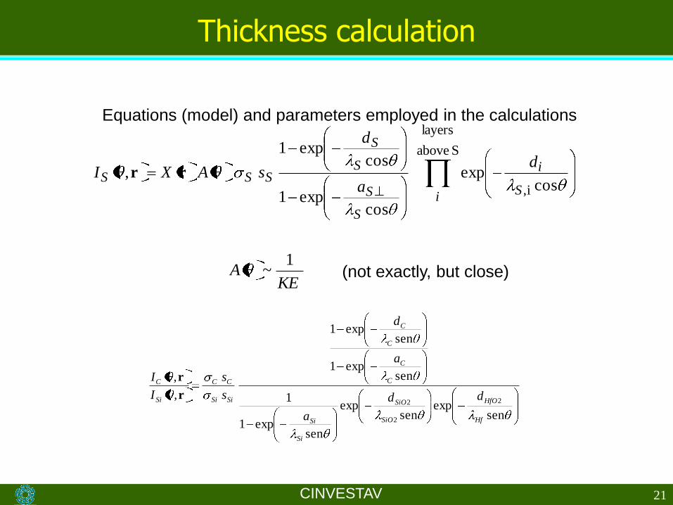
Thickness calculation
senexp
senexp
senexp1
1
senexp1
senexp1
,
,
2
2
2
Hf
HfO
SiO
SiO
Si
Si
C
C
C
C
SiSi
CC
Si
C
dd
a
a
d
s
s
I
I
r
r
S above
layers
i, cosexp
cosexp1
cosexp1
,
iS
i
S
S
S
S
SSSd
a
d
sAXI rr
Equations (model) and parameters employed in the calculations
KEA
1~ (not exactly, but close)
CINVESTAV 22
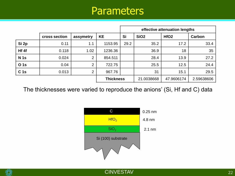
Parameters
SiO2 2.1 nm
4.8 nm
Si (100) substrate
C
HfO2
0.25 nm
effective attenuation lengths
cross section assymetry KE Si SiO2 HfO2 Carbon
Si 2p 0.11 1.1 1153.95 29.2 35.2 17.2 33.4
Hf 4f 0.118 1.02 1236.36 36.9 18 35
N 1s 0.024 2 854.511 28.4 13.9 27.2
O 1s 0.04 2 722.75 25.5 12.5 24.4
C 1s 0.013 2 967.76 31 15.1 29.5
Thickness 21.0038668 47.9606174 2.59638606
The thicknesses were varied to reproduce the anions’ (Si, Hf and C) data
CINVESTAV 23
Conclusions
•The annealing present a different phase of SiO2 and HfO2 moved the
binding energy.
•increasing the cycles number, the signal of O assotiated to HfO2
increase.
•TaN is not present after of removed in the samples annealing
•With annealing the N is going to entrance to lattice of the HfO2
•N 1s present a peak of correspond to NO2 is possible to introduce of
HfON, SiON or both of them.
•The thickness was calculated with the equation
CINVESTAV 24
Conclusiones
•Increase the SiO2 peak with annealing
•The suboxide in the Si 2p to continue increase with the temperature.
• We have a uniform and control in the grown of HfO2 films but is
formed a SiO2 in the interface of HfO2/Si.
• is possible to see the contribution of TaO and TaN respect the angle
resolution the Ta2O5 is on the surface and N of the TaN is depth.