department of physics, chemistry and biology22336/fulltext01.pdf · ment of physics, chemistry and...
TRANSCRIPT

Department of Physics, Chemistry and Biology
Master’s Thesis
Numerical calculations of optical structures using FEM
Henrik WiklundLITH-IFM-EX--06/1646--SE
Department of Physics, Chemistry and BiologyLinköpings universitet
SE-581 83 Linköping, Sweden

Master’s ThesisLITH-IFM-EX--06/1646--SE
Numerical calculations of optical structures using FEM
Henrik Wiklund
Supervisor: Hans Arwinifm, Linköpings universitet
Examiner: Kenneth Järrendahlifm, Linköpings universitet
Linköping, 22 September, 2006


Avdelning, InstitutionDivision, Department
Applied OpticsDepartment of Physics, Chemistry and BiologyLinköpings universitetSE-581 83 Linköping, Sweden
DatumDate
2006-09-22
SpråkLanguage
Svenska/Swedish Engelska/English
RapporttypReport category
Licentiatavhandling Examensarbete C-uppsats D-uppsats Övrig rapport
URL för elektronisk version
http://urn.kb.se/resolve?urn:nbn:se:liu:diva-7326
ISBN—
ISRNLITH-IFM-EX--06/1646--SE
Serietitel och serienummerTitle of series, numbering
ISSN
—
TitelTitle
Numeriska beräkningar av optiska strukturer med FEMNumerical calculations of optical structures using FEM
FörfattareAuthor
Henrik Wiklund
SammanfattningAbstract
Complex surface structures in nature often have remarkable optical properties.By understanding the origin of these properties, such structures may be utilizedin metamaterials, giving possibilities to create materials with new specific opticalproperties. To simplify the optical analysis of these naturally developed surfacestructures there is a need to assist data analysis and analytical calculations withnumerical calculations.
In this work an application tool for numerical calculations of optical prop-erties of surface structures, such as reflectances and ellipsometric angles, has beendeveloped based on finite element methods (FEM). The data obtained from theapplication tool has been verified by comparison to analytical expressions in athorough way, starting with reflection from the simplest of interfaces stepwiseincreasing the complexity of the surfaces.
The application tool were developed within the electromagnetic module ofComsol® Multiphysics and used the script language to perform post-processcalculations on the obtained electromagnetic fields. The data obtained from thisapplication tool are given in such way that easily allows for comparison with datareceived from spectroscopic ellipsometry measurements.
NyckelordKeywords optics, optical structures, ellipsometry, FEM, Comsol Multiphysics


AbstractComplex surface structures in nature often have remarkable optical properties.By understanding the origin of these properties, such structures may be utilizedin metamaterials, giving possibilities to create materials with new specific opticalproperties. To simplify the optical analysis of these naturally developed surfacestructures there is a need to assist data analysis and analytical calculations withnumerical calculations.
In this work an application tool for numerical calculations of optical propertiesof surface structures, such as reflectances and ellipsometric angles, has been de-veloped based on finite element methods (FEM). The data obtained from theapplication tool has been verified by comparison to analytical expressions in athorough way, starting with reflection from the simplest of interfaces stepwise in-creasing the complexity of the surfaces.
The application tool were developed within the electromagnetic module of Comsol®Multiphysics and used the script language to perform post-process calculations onthe obtained electromagnetic fields. The data obtained from this application toolare given in such way that easily allows for comparison with data received fromspectroscopic ellipsometry measurements.
v


AcknowledgementsThis master’s thesis has been done at the Laboratory of Applied Optics, Depart-ment of Physics, Chemistry and Biology, Linköping University, during the periodMarch to September 2006. First of all I would like to thank the support teamat Comsol AB, especially Magnus Olsson, who patiently answered my questionsand helped me to use Multiphysics in an efficient way. I would like to thankeveryone at the Laboratory of Applied Optics, especially my examiner KennethJärrendahl and supervisor Hans Arwin for their support and guidance during thiswork, above all for their constructive comments during the process of writing thisreport. I would also like to thank Sabyasachi Sarkar for the company during thelate evenings spent at the department. Finally my thanks go to my family andfriends whose support made this work possible.
vii


Contents
1 Introduction 11.1 Background . . . . . . . . . . . . . . . . . . . . . . . . . . . . . . . 11.2 Task . . . . . . . . . . . . . . . . . . . . . . . . . . . . . . . . . . . 21.3 Thesis outline . . . . . . . . . . . . . . . . . . . . . . . . . . . . . . 21.4 Summary . . . . . . . . . . . . . . . . . . . . . . . . . . . . . . . . 2
2 Theory 32.1 Electromagnetism . . . . . . . . . . . . . . . . . . . . . . . . . . . . 3
2.1.1 Maxwell’s equations . . . . . . . . . . . . . . . . . . . . . . 32.1.2 Polarized light . . . . . . . . . . . . . . . . . . . . . . . . . 52.1.3 Describing materials . . . . . . . . . . . . . . . . . . . . . . 52.1.4 Controlling electromagnetic properties . . . . . . . . . . . . 82.1.5 Reflectance . . . . . . . . . . . . . . . . . . . . . . . . . . . 102.1.6 Far-field approximation . . . . . . . . . . . . . . . . . . . . 15
2.2 Numerical calculations . . . . . . . . . . . . . . . . . . . . . . . . . 162.2.1 Finite Element Method (FEM) . . . . . . . . . . . . . . . . 172.2.2 Electromagnetic boundary conditions . . . . . . . . . . . . 172.2.3 Periodic boundary conditions . . . . . . . . . . . . . . . . . 212.2.4 Perfectly matched layers . . . . . . . . . . . . . . . . . . . . 212.2.5 Total field formulation . . . . . . . . . . . . . . . . . . . . . 222.2.6 Scattered-field formulation . . . . . . . . . . . . . . . . . . 232.2.7 Error estimation . . . . . . . . . . . . . . . . . . . . . . . . 252.2.8 Comsol® Multiphysics . . . . . . . . . . . . . . . . . . . . . 252.2.9 Comsol® Script . . . . . . . . . . . . . . . . . . . . . . . . . 26
2.3 Optical Measurements by spectroscopic ellipsometry . . . . . . . . 262.4 Summary . . . . . . . . . . . . . . . . . . . . . . . . . . . . . . . . 27
3 Results and discussion 293.1 Model development . . . . . . . . . . . . . . . . . . . . . . . . . . . 29
3.1.1 General configuration . . . . . . . . . . . . . . . . . . . . . 303.2 Two-phase system . . . . . . . . . . . . . . . . . . . . . . . . . . . 35
3.2.1 The model . . . . . . . . . . . . . . . . . . . . . . . . . . . 353.2.2 Calculation results . . . . . . . . . . . . . . . . . . . . . . . 36
3.3 Three-phase system . . . . . . . . . . . . . . . . . . . . . . . . . . 42
ix

x Contents
3.3.1 The model . . . . . . . . . . . . . . . . . . . . . . . . . . . 423.3.2 Calculation results . . . . . . . . . . . . . . . . . . . . . . . 43
3.4 Four-phase system . . . . . . . . . . . . . . . . . . . . . . . . . . . 533.4.1 The model . . . . . . . . . . . . . . . . . . . . . . . . . . . 533.4.2 Calculation results . . . . . . . . . . . . . . . . . . . . . . . 54
3.5 Lateral modulated model . . . . . . . . . . . . . . . . . . . . . . . 593.5.1 The model . . . . . . . . . . . . . . . . . . . . . . . . . . . 593.5.2 Calculation results . . . . . . . . . . . . . . . . . . . . . . . 60
3.6 Summary . . . . . . . . . . . . . . . . . . . . . . . . . . . . . . . . 63
4 Conclusions and future work 654.1 Conclusions . . . . . . . . . . . . . . . . . . . . . . . . . . . . . . . 654.2 Future work . . . . . . . . . . . . . . . . . . . . . . . . . . . . . . . 65
4.2.1 Enhanced techniques . . . . . . . . . . . . . . . . . . . . . . 664.2.2 More advanced modeling . . . . . . . . . . . . . . . . . . . 66
4.3 Summary . . . . . . . . . . . . . . . . . . . . . . . . . . . . . . . . 67
Bibliography 69
A Appendix 71A.1 Left Handed Materials . . . . . . . . . . . . . . . . . . . . . . . . . 71
A.1.1 History . . . . . . . . . . . . . . . . . . . . . . . . . . . . . 71A.1.2 Application areas . . . . . . . . . . . . . . . . . . . . . . . . 73
List of Figures 74
List of Tables 75

Chapter 1
Introduction
Complex surface structures in nature often have remarkable optical properties,many of these are not yet fully understood. By understanding the origin of theseproperties, such structures can be used in new materials, giving possibilities toobtain specific optical properties, chosen by design, in new materials. To enhanceand simplify the process of analyzing these naturally occurring structures and thedesign of new materials, there is a need to assist data analysis and analyticalcalculations with advanced simulations in this field.
1.1 Background
The intriguing optical properties found on butterflies (Lepidoptera) and beetles(Coleoptera) have for some time been at interest for the Laboratory of AppliedOptics at Linköping University. During the discussing leading to this thesis, somedifferent topics were proposed. For example an investigation of the optical proper-ties of the wings of the butterflies Morpho rhetenor as well as studies on the rathernew left handed materials, i.e. materials with negative index of refraction, werediscussed. A common factor for these topics were the possibility to use numericalcalculations as a complement to ellipsometry measurements. This led to the ideaof developing an application tool for numerical calculations of the optical proper-ties of surface structures. The program used in this work, Comsol® Multiphysics,were chosen since knowledge about the product already existed within the group.
To be able to understand which effects shown in simulations arising from limi-tations in the model and which ones representing the properties of the modeledstructure it is important to explore and understand these limitations during thedevelopment process, so that the future result obtained from this application toolcan be trusted.
1

2 Introduction
1.2 TaskThe objective of this thesis was to develop an application tool for two-dimensionalfinite-element calculations of optical properties of surface structures. The correct-ness of the application tool should be verified in a thorough way by comparisonwith available analytical expressions, starting with the simplest of interfaces andthere after increasing the complexity stepwise. The final goal was to develop anapplication tool which later on shall be utilized to analyze naturally occurring com-plex surface structures, e.g. the structure on the wings of the butterfly Morphorhetenor.
1.3 Thesis outlineChapter 2 This chapter covers the basic theory used in this thesis. It covers
both the theory of electromagnetism and the basics of numerical calculations,especially the finite element method. A short introduction to ellipsometry isalso given at the end.
Chapter 3 Here the result from the calculations made during the process ofdevelopment are presented together with a discussion about the accuracyfor the different models. The accuracy is shown with both error-estimatingcalculations presented in tables and visual verification of the accuracy by theuse of figures.
Chapter 4 This chapter contains a conclusion of the overall performance ofthe developed application tool. The known limitations are described andguidelines for the use of the tool are presented. Future possibilities, both interms of more advanced calculation techniques and different ways to describethe optical properties, as well as new structures to do calculations of, are alsopresented in this chapter.
Appendix A A short description of the history of the concept metamaterialsand some of its possible applications are presented in the appendix.
1.4 SummaryIn this chapter the purpose and goal of this thesis has been described. In the nextchapter the basic theory of electromagnetism and numerical calculations will bepresented and discussed. The models which have been used are described and theanalytical expression for their optical properties are presented.

Chapter 2
Theory
This chapter will give a brief overview of the theory used within this report. Itwill treat the classical theory of electromagnetism and the finite element method(FEM), which are the two basic parts of this thesis. Since the results given by thecalculations mostly are to be compared to data measured with ellipsometry thattopic will also be briefly discussed here.
2.1 Electromagnetism
The basics for the application tool that have been developed in this work is thetheory of electromagnetism. It is the equations unified by Maxwell that are usedwhen the propagation and reflection of light is numerically calculated within theFEM based solver. This section will very briefly describe the basics of electromag-netism and try to give an overview of the physics behind the equations that areutilized in the models. The interaction between the electromagnetic wave and dif-ferent media will be discussed in some detail, as well as the possibilities to controlthese properties by for example designing surface structures. Even though it iscommon to use CGS-units in electromagnetism, SI-units will be used all throughthe thesis.
2.1.1 Maxwell’s equations
In 1873 Maxwell [1] published a unified theory of electromagnetism, which today isrecognized as classical electromagnetism. The four equations known as Maxwell’sequations were developed by different physicists during the 19’th century, butMaxwell put them together and wrote them in a unified, modern, mathematicalform. Maxwell’s equations describe the behavior of the electromagnetic fields andtheir interaction with matter. In the general case, and written on differential form,
3

4 Theory
the equations are,
∇ ·D = ρ (2.1)∇ ·B = 0 (2.2)
∇×H =∂D∂t
+ J (2.3)
∇×E = −∂B∂t
(2.4)
The four fields here are the electric displacement field D, the electric field E,the magnetic flux density B and the magnetic field H. J is the current densityand ρ is the charge density. The equations describe, respectively, how electricfields are produced by electric charges, the absence of a similar ”magnetic charge”,how magnetic fields are produced by currents and changing electric fields andhow changing magnetic fields produce electric fields. The relation between thedielectric displacement field and the electric field, as well as the relation betweenthe magnetic flux density and the magnetic field will be described in some detaillater on.
Plane waves
It can rather easily be shown that one solution to Maxwell’s equations is a har-monic oscillation, e.g. a plane wave. The electric field, the magnetic field and thedirection of propagation given by the propagation vector q, are then orthogonalto each other and form a right-hand system. The amplitudes of the fields will alsobe proportional to each other according to,
E0 = cµH0 (2.5)
where c is the speed of light in the media and µ is the permeability. The electricfield amplitude E0 and the magnetic field amplitude H0 are defined by,
E = E0ei(ωt−q·r) (2.6)
H = H0ei(ωt−q·r) (2.7)
In the equation above ω is the angular frequency and r is the coordinate vector.Since the electric and magnetic fields in a plane wave are connected in such way,it is not necessary to describe all fields explicitly. This is used in the applicationtool, where the z-part of the electric and magnetic fields are used together withthe wavelength and the direction of propagation to describe the fields.
Electromagnetic spectrum
The electromagnetic spectrum is divided into different classes of radiation. Radiowaves are example of radiation in the longer wavelength regions, with wavelengthsin the range of 103 to 108 m. On the other side of the spectrum X-rays withwavelengths in the range 10−8 to 10−11 m and γ-rays with wavelengths below10−11 m are found. The wavelengths of interest for this thesis are in the visibleand near infrared regions, i.e. between ∼ 400 nm and ∼ 1000 nm.

2.1 Electromagnetism 5
2.1.2 Polarized lightIt is necessary to describe the orientation of the fields in a propagating electromag-netic wave, i.e. the polarization, especially when studying reflection from surfaces.This is done by dividing the fields into two components, usually with the planeof incidence as reference. The plane of incidence is defined by the propagationvectors of the incident, reflected and refracted waves when studying reflection/-transmission at surfaces. When no oblique reflection or incidence occurs, a planeof propagation is chosen in such way that it simplifies the description of the polar-ization. The two components are the p-component, for which the electric field liesin the plane, and the s-component where the electric field is perpendicular to theplane. For light with angle of incidence θ0 the p- and s-components are defined asshown in Fig. 2.1.
N0
θ0 θ0
θ1
EtpHtp
N1
Eip
Hip
Erp
Hrp
x^
y^
z^
(a) p-components
N0
θ0
Ets
Hts
N1
Eis
His Hrs
Ers
θ0
θ1
(b) s-components
Figure 2.1: The p-polarized (a) and the s-polarized (b) parts of the re-flected, transmitted and incident fields in reflection from a single surfacewith complex refractive index N0 of the ambient medium and N1 of thesubstrate. The angle of incidence θ0 equals the angle of reflection, and θ1is the angle of refraction.
For light propagating in an x-y-plane, as in the system above, the relation be-tween the coordinate-based and the polarization-based description of the incidentand reflected fields are,
Eix = Eip cos θ0 Erx = −Erp cos θ0Eiy = Eip sin θ0 Ery = Erp sin θ0Eiz = Eis Erz = Ers.
(2.8)
2.1.3 Describing materialsWhen considering an electromagnetic wave propagating through a medium, it isnecessary to describe the way the electric and magnetic fields interacts with the

6 Theory
material. Since the wavelengths of interest in this work are much larger than thesize of the atoms, the atomic details in the interaction can be averaged into param-eters more easily applied to general cases. The interaction with the electric fieldcan be described with the electric permittivity ε, whereas the magnetic permeabil-ity µ describes the interaction with the magnetic field. These two electromagneticparameters gives the complex refractive index N which for example easily canbe connected to the speed of propagation of the wave or the way it refracts andreflects at interfaces.
Permittivity – ε
The physical quantity permittivity, or electric permittivity, for a material describeshow an electric field affects and is affected by a medium, i.e. it describes thematerials ability to polarize in response to an applied electric field. Permittivityhas the SI-units Farad per meter [F/m], and it gives the relationship between theelectric displacement field D and the electric field E. It is usually complex valuedand it varies with the angular frequency ω of the fields,
D = εE = ε (ω)E = (ε′ (ω)− iε′′ (ω))E (2.9)
To give a rather simple description of how the permittivity may change with fre-quency one can think of the atoms and molecules as a set of harmonically boundelectron oscillators with a resonance frequency ω0. An electric field with a fre-quency far below ω0 will displace the electrons from the atom core, inducing apolarization in the same direction as the field. As the frequency increases towardsthe resonant frequency, the electrons will be displaced further and further awayfrom the nuclei cores, inducing a higher and higher polarization. Near the resonantfrequency the polarization will be very large, and when the frequency of the fieldis larger than ω0 the stored energy within the oscillations will be too large and theelectrons response will be out of phase, i.e. there will be a negative response. Witheven higher frequencies the response will be of much lower amplitude, decreasingtowards zero response, although it becomes positive again.
Usually, in frequency-regions where the real part of the permittivity is negative,no propagating electromagnetic waves exist. In such regions the material is saidto show metallic properties. For regions where the real part is positive, electro-magnetic waves can propagate and the material is said to be dielectric.
The imaginary part of the permittivity ε′′, represents the phase difference betweenthe fields, and since such a delay of the response leads to losses the imaginary partalso is a description of the attenuation.
The permittivity of a material is normally presented by the relative permittiv-ity εr, given by,
ε = εrε0 or εr =ε
ε0(2.10)
where ε0 is the permittivity of free space, 8.854 · 10−12 F/m.

2.1 Electromagnetism 7
Permeability – µ
Permeability, or magnetic permeability, is the degree of magnetization of a mate-rial that responds linearly to an applied magnetic field, i.e. it gives the relationshipbetween the magnetic flux density B and the auxiliary field strength H. The SI-unit of permeability is Henry per meter, [H/m]. Just like the permittivity it isfrequency dependent and it may be complex valued,
B = µH = (µ′ (ω)− iµ′′ (ω))H (2.11)
As in the case of permittivity, the imaginary part represents the phase delay inthe response and may be related to the losses within the material. The frequencyvariation of magnetic response may be described with the harmonic oscillators asin the electric case, but now considering harmonically bound magnetic momentsinstead. It is usually said that µr = 1 for large frequencies, e.g. in the visiblerange, since the magnetic dipoles cannot follow the rapid oscillations of such mag-netic field.
The permeability of a material is most often given as the relative permeability,in the same way as the relative permittivity,
µ = µrµ0 or µr =µ
µ0(2.12)
where µ0 is the free space permeability, 4π · 10−7H/m. If the real part of thepermeability is negative the medium will be opaque for electromagnetic waves,just as the case for permittivity.
Refractive index – N
The complex refractive index N is the most commonly used parameter to describeoptical properties of a medium, at least in elementary ray optics. It easily givessuch electromagnetic properties as the phase velocity νp, the group velocity νg,and the refraction of a rays passing through an interface according to Snell’s law.It is defined as,
N = ±√εrµr (2.13)
The sign is here determined by requirements of causality (see appendix A.1). Sinceboth ε and µ are frequency dependent and generally complex valued, the generalform is,
N = n (ω)− ik (ω) (2.14)
Here n is then the ordinary index of refraction and k is the extinction coefficient.Just like the name indicates, the extinction coefficient describes how the wavedecays within the medium, according to,
E (z) = E (0) ekz (2.15)

8 Theory
where z is the direction of propagation. Considering real valued permittivity andpermeability in eq. 2.13 on the preceding page, it is seen that if either εr or µr
are negative, the refractive index will be complex valued, i.e. the medium will beopaque. But if both have the same sign, N will be real-valued and the materialwill be non absorbing.
2.1.4 Controlling electromagnetic propertiesIn the same way as the individual atoms can be averaged out due to the largedifference in size between the atoms and the wavelength of electromagnetic wavesup to at least the infrared region, it is possible to replace the detailed interactionof more complex collections of structures with effective parameters of the samekind, as long as the size of the structures is smaller than the wavelength. Theartificially created material, the metamaterial, can then be seen as a homogenousmaterial with new effective parameters. For example it is common to talk abouteffective permittivity εeff and effective permeability µeff when discussing opticalproperties of metamaterials. In later years new ways to design materials have beeninvented, giving large possibilities for the physicist to, to some extent, control thepermittivity and permeability after their own choice.
Applications
There are many different useful applications for materials with optical propertieswhich has been controlled by design. It is for example possible to create a mate-rial with a specific refractive index and with matched optical impedance towardsanother material. The optical impedance is defined as,
Z =õ
ε, and Z0 =
õ0
ε0(2.16)
where Z0 is the optical impedance of free space. Surfaces with matched opticalimpedance, i.e. the optical impedance of the substrate and the optical impedanceof the ambient media are equal, will not give rise to any reflection, and may therebybe used as antireflection coatings. Such coatings would be most useful in forexample fiber optics. When constructing a metamaterial which has simultaneouslynegative permittivity and permeability the material will have a negative refractiveindex. These new so called left handed materials have a wide range of new anduseful applications which currently are under exploration. A short description ofthe development of these materials and some possible applications will be givenbelow, and some further information can be found in appendix A.1 on page 71.
History
In the science of condensed matter it is common to reduce the complexity ofphenomenons by introducing composites. These composites consist of elementarybuilding blocks of materials which behave according to some simplified dynamics.One of these composites is the plasmon, a collective oscillation of the electron den-sity relative to the atom cores. These oscillations have a resonant frequency called

2.1 Electromagnetism 9
the plasma frequency, ωp. As discussed above it is close to the resonant frequency,or plasma frequency, that negative permittivity occurs. The plasma frequency isusually in the ultraviolet region of the spectrum. In 1996, a theoretical way [2] tobring the plasma frequency in a medium down to the GHz band was introduced.By construction of a metamaterial consisting of grids of thin metallic wires of theorder of 1 µm in radius the plasma frequency could be depressed up to 6 orders ofmagnitude. This effect is achieved since the effective mass meff of the electronsbecome as heavy as nitrogen atoms due to the narrowness of the wires, and dueto that ω2 is proportional to 1/meff .
In 1999, Pendry et al. [3] showed how to introduce a magnetic response into meta-materials by using special structures with the shape of a split ring of non-magneticmaterials. In these materials an external applied magnetic field induces a current,which due to the structure produces an effective magnetic response. They pre-dicted that this Split Ring Resonant (SRR), see Fig. 2.2, with a diameter of a fewmillimeters would get a magnetic resonance frequency a bit above 10GHz. Thiswas later experimentally verified by Smith et al. [4].
Figure 2.2: A Split Ring Resonant (SRR), which has been introduced byPendry et al. [3] and first fabricated by Smith et al. [4], in which currentsmay be induced when interacting with electromagnetic waves of specificwavelengths. The induced currents give rise to a magnetic response to theelectromagnetic wave in frequency regions much higher than in naturallyoccurring materials.
To be able to control the optical properties at higher frequencies, e.g. in the opticalregion, the size of these structures has to be decreased into the nanometer scale.This has, with some success, been done by Grigorenko et al. [5] by placing smallgold nano-pillars in pairs upon a surface, which gave a similar result as the wiresand SRRs. Another, more complex structure, was created by Shalaev et al. [6, 7]when they placed pairs of nano-rods upon each other in a specific pattern.
One possible application area for the tool developed during this work would be tosimplify the development of new surface structures with this kind of properties.

10 Theory
Microstructures
To change the effective permittivity and/or permeability of the material is not theonly way to change the optical properties of a surface. For example the reflectionsof a microstructure can create optical properties of the surface that otherwisewould be impossible to achieve by just designing the optical properties of thematerials used. Such microstructures are common on the wings of butterflies,where complex microstructure creates ultra-high visibility and polarization effectsinduced by reflectivity. There are many microstructures created by nature thatnot yet are fully analyzed and understood. One of those are the structure on thewings of Morpho rhetenor, which is one of many microstructures that Vukusic etal. [8] are analyzing. The wings of the Morpho rhetenor have a complex multilayer-like structure that might be described as two-dimensional Christmas trees on thesurface, which give rise to interesting optical effects, e.g. a strong reflection of bluelight.
2.1.5 ReflectanceThe information extracted from the calculations in this work are the relationshipbetween the incident and reflected fields. To verify the tool it is necessary toknow what results to expect. From the simple cases, this can usually be expressedanalytically. The Fresnel’s equations are used when modeling layered structures.For models with a lateral modulated layer an effective media approximation (EMA)is used in addition. When doing measurements in optics, the parameter usuallyobtained is the intensity. Therefore the reflectance is the value extracted from thesimulations. During this work the Fresnel’s reflection coefficients will be denotedr whereas the total reflection coefficients will be denoted R. The reflectance willbe denoted R, and the relation between these parameters are,
R =IrIi
=(Er
Ei
)2
= |R|2 (2.17)
where Ir and Ii are the reflected and incident intensities, respectively.
Two-phase systems
For the most simple case, a two-phase system (ambient-substrate), the Fresnel’sequations are used in their original form. Fig. 2.1 show a two-phase system withall the reflected and transmitted parts of the fields marked out.
rp =Erp
Eip=N1 cos θ0 −N0 cos θ0N1 cos θ0 +N0 cos θ0
=tan (θ1 − θ0)tan (θ1 + θ0)
(2.18)
rs =Ers
Eis=N0 cos θ0 −N1 cos θ0N0 cos θ0 +N1 cos θ0
=sin (θ1 − θ0)sin (θ1 + θ0)
(2.19)
These equations relate the p- and s-components of the reflected fields, Erp andErs, to the components of the incident fields, Eip and Eis.

2.1 Electromagnetism 11
Three-phase systems
When expanding to a three-phase system (ambient-layer-substrate) as shown inFig. 2.3 on the next page, and thereby taking another reflecting interface intoaccount, the relationship between the reflected and incident fields, i.e. the totalreflection coefficients, will be described by,
Rp =Erp
Eip=
r01p + r12pe−i2β
1 + r01pr12pe−i2β(2.20)
Rs =Ers
Eis=
r01s + r12se−i2β
1 + r01sr12se−i2β, (2.21)
(2.22)
where rlmp is the Fresnel’s coefficient rp (eq. 2.18) between the phases l and m,and β is the film phase thickness, which is given by,
β =2πdλN1 cos θ1 (2.23)
Here N1 is the complex index of refraction of the middle media, d is the thicknessof the layer and θ1 the angle of refraction. In Fig. 2.3 the components of thereflected and transmitted fields are shown individually. The total reflected field isthe sum over all its components according to,
Erp =∞∑
j=1
Erp,j (2.24)
Ers =∞∑
j=1
Ers,j (2.25)
n-phase systems
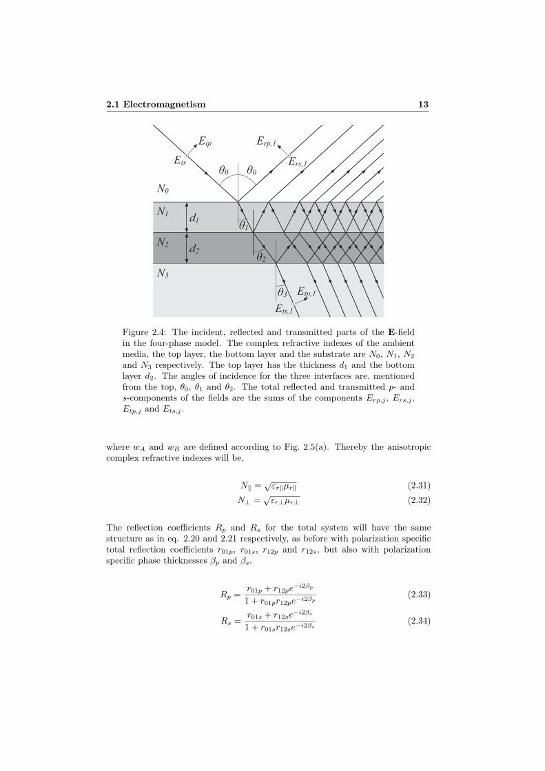
When adding further layers in the model the complexity of the analytical expres-sion for the reflectivity will increase rapidly. The expressions in eq. 2.26 and 2.27are for the case of a four-phase system, shown in Fig. 2.4. When dealing with morelayers a more flexible description, using matrices, are applied. Since this applica-tion tool only has been tested up to a four-phase system, that matrix descriptionis left out.
Rp =Erp
Eip=
[r01p + r12pe
−i2β1]+[r01pr12p + e−i2β1
]r23pe
−i2β2
[1 + r01pr12pe−i2β1 ] + [r12p + r01pe−i2β1 ] r23pe−i2β2(2.26)
Rs =Ers
Eis=
[r01s + r12se
−i2β1]+[r01sr12s + e−i2β1
]r23se
−i2β2
[1 + r01sr12se−i2β1 ] + [r12s + r01se−i2β1 ] r23se−i2β2(2.27)

12 Theory
N0
d
N1
N2
θ0 θ0
θ1
θ2
Eis Ers,1
Erp,1
Ers,2
Erp,2Eip
Ets,1
Etp,1
Ets,2
Etp,2
Figure 2.3: The incident, reflected and transmitted parts of the E-field inthe three-phase model. The complex index of refraction of the ambientmedia, the layer and the substrate are N0, N1 and N2 respectively. d isthe thickness of the layer. The angle of incidence at the upper interfaceis θ0 and θ1 at the lower interface. The total reflected and transmittedp- and s-components of the fields are the sums of the components Erp,j ,Ers,j , Etp,j and Ets,j .
Lateral modulated models
When modeling a laterally modulated surface layer according to Fig. 2.5(a), i.e. amicrostructured surface layer consisting of the materials A and B with all internalboundaries orthogonal to the surface, the normal treatment used above will not besufficient for an analytical expression of the reflectivity. An anisotropic descrip-tion has to be used to describe the optical properties of the modulated layer, seeFig. 2.5(b).
It can be shown that the macroscopic averages of the permittivity for the twoextreme cases, shown in Fig. 2.6, when the applied electromagnetic field is paralleland normal respectively to the internal boundaries, are given by,
ε‖ = fAεA + fBεB (2.28)
ε⊥ =1
fA
εA+ fB
εB
(2.29)
where fA and fB are the fractions of material A and B respectively, i.e.
fA =wA
wA + wB, fB =
wB
wA + wB, (2.30)
2.1 Electromagnetism 13
N0
θ0
d1
Eip
Eis Ers,1
Erp,1
Etp,1
Ets,1
N1
N2
N3
θ0
θ1
θ2
θ3
d2
Figure 2.4: The incident, reflected and transmitted parts of the E-fieldin the four-phase model. The complex refractive indexes of the ambientmedia, the top layer, the bottom layer and the substrate are N0, N1, N2
and N3 respectively. The top layer has the thickness d1 and the bottomlayer d2. The angles of incidence for the three interfaces are, mentionedfrom the top, θ0, θ1 and θ2. The total reflected and transmitted p- ands-components of the fields are the sums of the components Erp,j , Ers,j ,Etp,j and Ets,j .
where wA and wB are defined according to Fig. 2.5(a). Thereby the anisotropiccomplex refractive indexes will be,
N‖ = √εr‖µr‖ (2.31)
N⊥ =√εr⊥µr⊥ (2.32)
The reflection coefficients Rp and Rs for the total system will have the samestructure as in eq. 2.20 and 2.21 respectively, as before with polarization specifictotal reflection coefficients r01p, r01s, r12p and r12s, but also with polarizationspecific phase thicknesses βp and βs.
Rp =r01p + r12pe
−i2βp
1 + r01pr12pe−i2βp(2.33)
Rs =r01s + r12se
−i2βs
1 + r01sr12se−i2βs(2.34)

14 Theory
N0
N1A
N2
N1B d
wA wB
θ0
Eip
EtpEts
Eis Ers
Erp
θ0
θ2
(a) Laterally modulated layer
N0
dN1
N2
θ0 θ0
θ2
Eis Ers,1Erp,1
Ers,2Erp,2Eip
Ets,1
Etp,1Ets,2
Etp,2
N1
(b) Anisotropic layer
Figure 2.5: a) A laterally modulated thin layer with the two compositematerials A and B, with the complex refractive indexes N1A and N1B
respectively, and the width of the composites are dA and dB . d is thethickness of the thin layer, θ0 the angle of incidence and θ2 is the angleof refraction for the lower interface. The refractive index of the ambientis N0 and for the substrate N2. b) The anisotropic model of the laterallymodulated thin layer, where the composite layer has been replaced by ananisotropic medium with the complex refractive index N1‖ in the directionparallel to the surface, and N1⊥ in the perpendicular direction. The totalreflected and transmitted p- and s-components of the fields are as usualthe sums of the components Erp,j , Ers,j , Etp,j and Ets,j respectively.
εA εB
wA wB
E
(a) The parallel microstructure
εA
εB
wA
wB
E
(b) The perpendicular mi-crostructure
Figure 2.6: The two extremes for a composite material. a) All boundariesin the composite are parallel to the applied electric field E. For this casethe effective permittivity will be a volume average of the two composites.b) All boundaries are perpendicular to the applied electric field E. In thiscase the material with the lowest permittivity will dominate by screeningeffects.

2.1 Electromagnetism 15
where the single interface reflection coefficients and phase thicknesses are given by,
r01p =N1‖N1⊥ cos θ0 −N0
√N2
1⊥ −N20 sin2 θ0
N1‖N1⊥ cos θ0 +N0
√N2
1⊥ −N20 sin2 θ0
(2.35)
r12p = −N1‖N1⊥ cos θ2 −N2
√N2
1⊥ −N22 sin2 θ2
N1‖N1⊥ cos θ2 +N2
√N2
1⊥ −N22 sin2 θ2
(2.36)
r01s =N0 cos θ0 −
√N2
1‖ −N20 sin2 θ0
N0 cos θ0 +√N2
1‖ −N20 sin2 θ0
(2.37)
r12s = −N2 cos θ2 −
√N2
1‖ −N22 sin2 θ2
N2 cos θ2 +√N2
1‖ −N22 sin2 θ2
(2.38)
βp = 2πd
λ
N1‖
N1⊥
√N2
1⊥ −N20 sin2 θ0 (2.39)
βs = 2πd
λ
√N2
1‖ −N20 sin2 θ0 (2.40)
2.1.6 Far-field approximationWhen doing electromagnetic calculations of small structures, it is important toknow if the resulting field is a near-field or a far-field. Near-fields are fields closeto the structure and is dominated by evanescent waves whereas the far-field isfurther away and is dominated by propagating waves. A good example of thedifference between the two fields can be found in the double-slit experiment. Thenormally observed field, the far-field, has a well known intensity peak in the middleof the interference pattern, whereas Chae K-M et al. [9] have shown with numericalcalculations that the near-field has an intensity minimum at the center, i.e. thereis a phase shift of π between the two interference patterns. It is also important tonotice that no energy is transported by the evanescent waves in the near-field. Itis thereby most important to be sure of what kind of fields that are obtained fromthe calculations.
To ensure that it is the amplitude of the far-field that is retrieved from the cal-culations a far-field approximation can be performed. Such a transformation maybe useful when dealing with fields similar to the one in Fig. 2.7, where the am-plitude is rather complex close to the surface. In cases where reflections from ahomogenous wave scattered at a flat surface which is infinite and homogenous inx-direction, there is no need for a far-field approximation, since there will be nodifference in the structure of the field close to the surface and far away.
The reason why the far-field and not the near-field is the field of interest is thatthe result will be compared to measurements performed a few decimeters distance

16 Theory
Figure 2.7: The amplitude, shown as grayscale, of the reflected E-field atnormal incidence on a dielectric surface with gold nano-pillars placed inpairs.
away from the sample, which is in the far-field region. An approximation of thelimit, dfar, between the near-field and the far-field is,
dfar =2L2
λ(2.41)
where L is the period of the surface structure, or the dimension of an antenna.This is known as the ”antenna designer’s formula” [10].
An often used far field transformation is the Stratton-Chu formula [11], whichmain application area is radiation calculations of antennas. However, it is appli-cable on the type of field calculations in this work as well. In the Stratton-Chuapproximation the resulting computed electric far-field Ep, at point p, is given by,
Ep = R0 ×∫∫S
[n×Ea − ηR0 × (n×Ha)
]eiqa·R0dS (2.42)
where Ea and Ha are the fields at point a on the surface S, just outside thescattering surface. R0 is the unit vector pointing from the origin to the field pointp, n is the outward normal from the surface at point a. η is an impedance constantof free space, q is the free space wave number (2π/λ or |q|) and a is the vectorfrom the origin to the surface point a.
2.2 Numerical calculationsThe numerical calculations, or simulations, are done with the Finite ElementMethod (FEM) using the commercial software Comsol® Multiphysics. A two-

2.2 Numerical calculations 17
dimensional model of the surface is created and constraints and parameters areapplied on each subdomain and boundary. To get a model close to reality somedifferent methods are combined into an application tool that will have enough ac-curacy for our needs. In this section a rather brief introduction to FEM is givenfollowed by more detailed introductions to the additional methods that have beenapplied.
2.2.1 Finite Element Method (FEM)The finite element method is a numerical procedure for finding approximate solu-tions of partial differential equations (PDE) over a model with specified boundaryconditions. It is thereby a procedure that may be used to solve many differentkind of problems in physics. The principle of the method is to replace an entirecontinuous domain by a number of subdomains, called elements. In these elementsthe unknown continuous functions are represented by simple interpolation func-tions with unknown coefficients. By doing so the number of degrees of freedom arereduced to a finite number, i.e. the solution of the entire system is approximatedby a finite number of unknown coefficients. The solution is then obtained by linearor non-linear optimization. One major advantage of FEM is that the size of theelements can differ over the model, and thereby higher resolution and accuracycan be obtained at parts where so wanted, e.g. at interfaces or curves. It alsomakes it suitable for calculations in complex structures, which has lead to manyapplications in for example structural mechanics.
2.2.2 Electromagnetic boundary conditionsThe most important part of the model is the boundary conditions. These con-ditions describe how the interfaces affect and are affected by the electromagneticfields, e.g. induced surface currents. They may be divided into subgroups, theinternal and the external boundary conditions.
Internal boundaries
The internal boundaries are the ones inside the model, i.e. they have subdomainswith additional conditions on both sides. Here the subindexes 1 and 2 refers tothe subdomains on the different sides of the interface and n is the surface normal.
ContinuityIn the normal case the only condition to internal boundaries is the requirement ofcontinuity of the tangential components of the fields, i.e.
n× (E1 −E2) = 0n× (H1 −H2) = 0 (2.43)

18 Theory
Surface current and surface chargeWhen introducing a surface current on the boundary Js or a surface charge ρs
only some small adjustments have to be done in the eq. 2.43, according to,
n× (E1 −E2) =ρs
εn× (H1 −H2) = Js (2.44)
Impedance boundary conditionThe impedance boundary condition, also known as a mixed boundary condition,is used when the second medium is an imperfect conductor.
1µr1
n× (∇×E)− iq0η
n× (n×E) = 0 (2.45)
1εr1
n× (∇×H)− iq0ηn× (n×H) = 0 (2.46)
where
η =√µr2/εr2 and q0 = ω
√ε0µ0 (2.47)
This condition may sometimes [12] be useful to give in a more generalized way, byexchanging the constants iq0
η with a constant γe and introduce the term U on theright hand side according to,
1µr1
n× (∇×E)− γen× (n×E) = U (2.48)
External boundaries
The external boundaries are the ones that limit the model in size. They mayrepresent either limiting materials or open space.
Perfect electric/magnetic conductorThe conditions for either perfect electric or magnetic conductor are given by eq.2.49 and 2.50 respectively.
n×E = 0 (2.49)n×H = 0 (2.50)
NeutralFor boundaries which are both perfect electric and magnetic conductors, theboundary conditions are, consequently, given by,
(n×E) = 0, (n×H) = 0. (2.51)

2.2 Numerical calculations 19
Matched boundary conditionThe matched boundary is an open space boundary that may be used to introducea plane electromagnetic wave, E0 and H0, with the propagation constant β. Thistype of boundary also allows for radiation out of the model for plane waves withthe same direction of propagation as specified with the propagation constants.
n× (∇×E)− iβ (E− (n ·E) n) = −2iβ (E0 − (n ·E0) n) (2.52)n× (∇×H)− iβ (H− (n ·H) n) = −2iβ (H0 − (n ·H0) n) (2.53)
Weak formulation
The weak formulation, or variational method, is another way to solve the originalPDE problem. The Ritz method, also known as the Rayleigh-Ritz method [12], isone of the most commonly used variational methods within FEM. In this methodthe boundary-value problem is formulated in terms of a functional, i.e. a functionof functions. The governing differential equations for the problem corresponds tothe minimum of this functional, i.e. the solution can be obtained by minimizingthe functional with respect to a test function. Denoting the functional F and thetest function φ, which according to section 2.2.1 is described with a finite numberof coefficients corresponding to the interpolation functions within each element,the functional that is to be minimized can be written like,
F (φ) = F
(N∑
i=1
civi
)(2.54)
where N is the total number of coefficients, ci is the coefficient to the correspond-ing interpolation function vi. The test function φ which minimizes the functionalF is the solution to the problem.
Since the variational method is difficult to use without the computational powerprovided with computers, it is rather unusual to describe physical problems in thisway. For this reason it is most often necessary to obtain the functional F fromthe PDE description of the boundary-value problem. In the case of electrody-namics with complex values of the permittivity, permeability or boundary specificparameters like γ, the generalized variational principle have to be used for thiscalculation. The functional F is then given by,
F (φ) =12〈Lφ, φ〉 − 1
2〈Lφ, u〉+
12〈φ,Lu〉 − 〈φ, f〉 (2.55)
where the inner product is defined as,
〈φ, ψ〉 =∫Ω
φψdΩ (2.56)
The operator L and the function f are taken from the PDE written on the formin eq. 2.57. An example, the Poisson’s equation, is shown in eq. 2.58. u is the

20 Theory
non-vector version of the inhomogeneous vector term in the boundary conditioneq. 2.48 on page 18.
Lφ = f (2.57)
−∇ · (ε∇E) = ρ ⇒L = −∇ · (ε∇)f = ρ
(2.58)
In the case of vector functions the inner product is defined as,
〈a,b〉 =∫∫∫
V
a · bdV (2.59)
the function f is replaced by a vector function f and the inhomogeneous term uis replaced with U.
For a electromagnetic boundary-value problem defined by the vector wave equa-tion,
∇×(
1µr∇×E
)− q20εrE = −iqoZ0J (2.60)
on the volume V and a boundary condition on the boundary S according to eq.2.48 the weak form can be derived as,
F (E) =12
∫∫∫V
[1µr
(∇×E) · (∇×E)− q20εrE ·E]dV+
∫∫S
[γe
2(n×E) · (n×E) + E ·U
]dS
+iq0Z0
∫∫∫V
E · JdV (2.61)
Mesh
The mesh is the net which divides the model into a finite number of elements. Itcan be created in some different ways, but there are two methods which mainlyare used. One is unstructured with triangular elements and the other is structuredwith squared elements. Both methods have their advantages and disadvantages.For example, it is preferable to have equal meshes at boundaries linked by periodicboundary conditions (see Sec. 2.2.3), which may be accomplished by a structuredmesh. On the other hand such method of meshing will require that the subdomainsof the model all are fairly rectangular in shape. When using triangular elements,it is easier to have freely shaped geometries in the model. The unstructured wayhave another advantage in that the random orientation of the elements actuallyhelps minimizing phase-errors occurring due to for example numerical anisotropic

2.2 Numerical calculations 21
phase-velocities.
The number of finite elements used, how fine the mesh is, is most important.With too few elements the solution may not converge. On the other hand, if themesh is too fine, the simulation will take much more computational power thanactually needed. Since the meshing is very flexible in FEM, it is easy to use a finermesh at the parts of the model where this is needed, for example areas close tointerfaces. A rule of thumb is to have at least five to ten elements per wavelengthon open subdomains, and even denser close to surfaces and corners.
2.2.3 Periodic boundary conditionsWhen studying the optical properties of a surface structure, it would be convenientto work with an unlimited sample, so that no effects of the physical limitationsof the sample would interfere with the result. But when dealing with nano-sizedsurface structures it is not even reasonable to perform large scale surface simula-tions with ordinary computer power. This problem is possible to overcome withPeriodic Boundary Conditions (PBC), in the cases where the surface structurehas some kind of periodicity. The PBC links the sides opposite to each other andwill thereby, in a way, make the model infinitely long in that direction, repeatedwith the periodicity introduced in the condition linking the boundaries together.The PBC can be used to make the linked boundaries identical to each other,but it is often more convenient to introduce a different relationships between thetwo boundaries. Those, more generalized, conditions are sometimes called linkedboundary conditions.
When using models where the E-field only has one of the p- and s-components,the boundary conditions corresponding to perfect electric/magnetic conductors,eq. 2.49 and 2.50 are used for the boundaries where periodic boundary conditionsare applied. For models which have both components of the electric field, theneutral boundary condition, eq. 2.51 is used instead.
2.2.4 Perfectly matched layersIn some directions there might be an infinite continuation of the media. It is thennecessary to use a boundary condition which can represent this infinite continua-tion, also called open boundary. The best way to do this is to introduce a PerfectlyMatched Layer (PML).
The PML [13, 12] is used to limit the reflections from this kind of open, free-space,boundaries. They are expansions of the model in the directions where infinity isto be simulated. By changing the way that the permeability and permittivity aredefined for the subdomain, a gradually increasing absorption is achieved. Thisabsorption may also be seen as a coordinate transformation which makes the op-tical path length infinite. The typical length of the PML is about one wavelength,but this is of course a question of the quality needed in the simulation versus the

22 Theory
computational power that are available. For a PML that are to absorb radiationin the y-direction the permeability and permittivity matrices will be multipliedwith the following operator,
L =
Lxx 0 00 Lyy 00 0 Lzz
(2.62)
where,
Lxx =sysz
sxLyy =
szsx
syLzz =
sxsy
sz(2.63)
sx = 1 sy = a− ib sz = 1. (2.64)
For example the relative permittivity in such case would be given by,
εr = εrL =
εrLxx 0 00 εrLyy 00 0 εrLzz
(2.65)
The constants a and b are to be set depending on the size of the PML and howfine the mesh in that subdomain is. The smaller the subdomains are, the highervalue of the coefficients will be needed.
The attenuation of the field in the example above is described by,
|E| = |E0| e−bqy∆y (2.66)
when propagating over a distance ∆y with the y-component qy of the wave vectorq. The real part of sy will affect the additional absorption of the already decayingevanescent waves in the PML.
These PMLs would in an analytical solution not give any reflections at all. Thisis unfortunately not the case in numerical calculations, and some reflections willalways occur when using FEM. However, they are minimized to a very acceptablelevel with this implementation.
Within this report, no simulation where the substrate is a left hand material isperformed, but since it might be a natural development in the future, it is worthmentioning that the ordinary PML does not work if applied to such materials [14].Instead a modified version, especially made for left handed materials will have tobe applied.
2.2.5 Total field formulationThe most straight forward way to introduce an incident field is to introduce iton the outer (upper) boundary. The wave will then travel from this boundarydown towards the scattering surface, and the reflected wave will propagate up to-wards the upper boundary again. The solution provided by FEM is the total field

2.2 Numerical calculations 23
and the reflected wave may be distinguished by subtraction of the incident wavefrom the total field. This is not all too difficult, since the analytical expressionfor the incident wave is well defined. However, the propagation of the wave iscalculated numerically, and some difference between the analytical expression andthe simulated field will occur. This is usually a rather small difference, but sincethe amplitude of the incident field in many cases are considerably larger than theamplitude of the reflected field, such differences may have a significant influenceon the extracted information of the reflected field.
Another problem that might occur when using a total field formulation is whenthe method is combined with a PML. The incident wave will then be introducedabove the PML, and the amplitude of the wave will be drastically decreased onthe way down through the PML. This introduces a numerical uncertainty in theamplitude of the effective incident field, below the PML. Thereby the accuracy ofthe calculations is further decreased.
2.2.6 Scattered-field formulationAn alternative to the total field formulation is the scattered-field formulation [12,15], where the incident field is introduced directly on the scatterer. The imple-mentation of the scattered-field formulation uses the weak formulation (variationalcalculation).
When considering a volume V bounded by the surface S, the electromagneticfields generated by an internal current density Ji can be described with the curl-curl equation obtained from Maxwell’s equations,
∇×[
1µ∇×E
]+ ε
∂2E∂t2
+ σ∂E∂t
= −∂Ji
∂tr ∈ V (2.67)
where the magnetic field has been eliminated with aid of the constitutive relationsand σ is the conductivity of the media. By substituting E with Einc + Esc intoeq. 2.67 with Ji = 0, the incident field Einc may be separated from Esc accordingto,
∇×[
1µ∇×Esc
]+ ε
∂2Esc
∂t2+ σ
∂Esc
∂t=
= −∇×[
1µ∇×Einc
]− ε
∂2Einc
∂t2− σ
∂Einc
∂t(2.68)
The right hand side may now be replaced by an equivalent current source, Jeq
according to eq. 2.67, i.e.∂Jeq
∂t= ∇×
[1µ∇×Einc
]+ ε
∂2Einc
∂t2+ σ
∂Einc
∂t(2.69)
When applying eq. 2.69 in eq. 2.68,
∇×[
1µ∇×Esc
]+ ε
∂2Esc
∂t2+ σ
∂Ese
∂t= −∂Jeq
∂t(2.70)

24 Theory
Jeq is only nonzero in the region with µ, ε or σ are different from the ambientmedia, according to eq. 2.67 where Ji is zero due to the absence of currents.Together with an impedance boundary condition according to,
n×[
1µ∇×Esc
]+ Yc
∂
∂t[n× n×Esc] = 0 (2.71)
the weak form of eq. 2.70 will be,∫∫∫V
1µ
[∇×Ni] · [∇×Esc] + εNi ·∂2Esc
∂t2+ σNi ·
∂Esc
∂t+
+1µ
[∇×Ni] · [∇×Einc] + εNi ·∂2Einc
∂t2+ σNi ·
∂Einc
∂t
dV+
+∫∫S
Yc [n×Ni] ·
∂
∂t[n×Esc]−
1µ
[n×Ni] · [∇×Einc]dS = 0 (2.72)
where the intrinsic admittance of the infinite medium Yc is√ε/µ, Ni are the
interpolation vector functions and n is the outward normal to the surface S. Whenwritten on this form, the incident field is involved in the volume integral over theentire computational domain V as well as in the surface integral over S. To increasethe efficiency of the calculations, the knowledge of the incident field outside thescatterer, in terms of fulfilled equations, may be utilized to reduce the weak formto, ∫∫∫
V
1µ
[∇×Ni] · [∇×Esc] + εNi ·∂2Esc
∂t2+ σNi ·
∂Esc
∂t+dV+
+∫∫∫
Vs
1µ
[∇×Ni] · [∇×Einc] + εNi ·∂2Einc
∂t2+ σNi ·
∂Einc
∂t
dV+
+∫∫S
Yc [n×Ni] ·∂
∂t[n×Esc] dS+
−∫∫Ss
1µ
[ns ×Ni] · [∇×Einc] dS = 0 (2.73)
where Ss is the surface of the scatterer, Vs its volume and ns its outward normal.
From eq. 2.73 it is seen that the incident wave only will be introduced in theweak terms inside the scatterer and on its outer boundaries.
By introducing the incident wave into the weak formulation directly there willbe an increase in accuracy when extracting the amplitude of the reflected wave,since no subtraction will have to be made. On the other hand, when looking atthe transmitted field the incident field will have to be added to the result, sincethe field obtained from the finite element calculation will be the difference betweenthe total field and the incident field.

2.2 Numerical calculations 25
2.2.7 Error estimationIt is important for the verification process to have some quantities for determi-nation of the accuracy of the simulated data. The parameters which are to becompared for each model setup are the reflectances Rs and Rp as well as theparameters used in ellipsometry measurements, Ψ and ∆. These parameters arecalculated for each angle of incidence θ and wavelength λ.
Mean squared error
The method for estimating the accuracy throughout this thesis were chosen to bethe Mean Squared Error (MSE).
MSE =1
N + 1
N∑i=1
(Xri −Xci)2 (2.74)
where Xr is the reference (analytic) value, Xc the calculated value and N thenumber of points that are compared. The mean squared error is exactly what itseems to be, the mean value of the squared error in each point of measurement.To be able to get a single value for each model the sum is taken over both angleof incidence θ and wavelength λ. For an easier implementation the normalizationis changed from N + 1 to N , which is due to that the summation will have to bedivided into different steps. Since N usually is large, e.g. 13 wavelengths with 40angles of incidence each gives 520 evaluated points, this will have a very limitedeffect on the result.
MSE =1
Nλθ + 1
∑λ,θ
(Xrλθ −Xcλθ)2 ≈ 1
Nλ
∑λ
(1Nθ
∑θ
(Xrλθ −Xcλθ)2
)(2.75)
One advantage by using this error estimation is that it is also used in some ellip-sometry measurements, where parameters are adjusted to make a model fit themeasured data. As a complement to the single MSE value calculated for eachmodel, the extreme values of the MSE where only the angle is varied can also bepresented where so is needed. This data will help to discover if there are somewavelengths for which the model works less well.
2.2.8 Comsol® MultiphysicsThe program chosen as environment for the application tool is Comsol® Multi-physics ver. 3.2, from here on only referred to as Multiphysics. Multiphysics werein the beginning a PDE tool box for Mathworks MATLAB® which later became anadd-on application with the name FEMLAB®. The program is now independentbut still compatible with MATLAB®. It is a multipurpose FEM program whichcan be used for many different types of simulations within a wide range of areasin physics. In addition to the FEM solver, the program contains modules for thedifferent areas of physics. These modules have predefined sets of equations andvariables used for solving problems of the specified type. Multiphysics has also
26 Theory
a very strong advantage when it comes to linking problems from different areastogether.
2.2.9 Comsol® ScriptThe new version of Multiphysics contains the possibility to easily operate theprogram from a consol, just like FEMLAB® could be controlled from MATLAB®.This script approach gives more flexible ways for post processing the data obtainedfrom the solution, as well as doing sets of multiple simulations while varying alarger amount of parameters. It can be seen as a small version of the MATLAB®
interface, which is more than enough for the average user. It is also possible tocreate a graphical user interface of your own with the script language combinedwith JAVA, which opens up for large possibilities in creating your own specializedapplication tool with Multiphysics as backbone.
2.3 Optical Measurements by spectroscopic ellip-sometry
Ellipsometry is a commonly used optical technique for determining properties ofsurfaces and thin films. By studying the change of polarization when a monochro-matic plane wave is reflected at oblique incidence it is possible to determine thecomplex reflectance ratio, which is defined as
ρ =Rp
Rs=∣∣∣∣Rp
Rs
∣∣∣∣ ei(δp−δs) (2.76)
where Rp and Rs are the complex reflection coefficients for the p- and s- parts,respectively. ρ is usually expressed using the phase change, ∆, and the amplituderatio, tanΨ, where
tanΨ =∣∣∣∣Rp
Rs
∣∣∣∣ and ∆ = δp − δs (2.77)
i.e.
ρ = tan Ψei∆. (2.78)
By varying the angle of incidence, frequency and the polarization of the incidentwave enough information can be gathered to retrieve the electromagnetic prop-erties of the material, as well as the thickness of thin layers. Since the relativeamplitude change is a ratio between the p- and s-components the result will beindependent of the intensity of the source.

2.4 Summary 27
2.4 SummaryIn this chapter the basic theory of FEM has been discussed, including the weakformulation and the scattered-field formulation. The notations for the parametersthat are obtained from the calculations are defined, and the analytical expressionsfor the reflectance in the different models are displayed. In the next chapter thiswill be used to describe the development and verification process of the applicationtool. The obtained accuracy in the different models will also be shown.

28 Theory

Chapter 3
Results and discussion
This chapter will describe the steps performed during the process of developmentand verification of the application tool, i.e. the implementation of the theory de-scribed in Sec. 2. It begins with a section about the basic settings utilized in thetool and continues with separate sections for the different types of structures thathave been simulated.
The main purpose of the models created in this work is to verify the accuracyof the obtained result. Due to this, the focus will be to find out where the cal-culations start to differ from the analytical expressions, and if possible, ways tomodify the models so that the differences may be minimized. If the accuracy forsome cases can not be verified, it is important to map out the limits so that theresults obtained from unknown structures can be trusted. Unfortunately, it is notpossible to do simulations with all different combinations of parameters, but thesimulations presented in this chapter are selected so that they will cover as largerange of combinations as possible.
3.1 Model developmentTo obtain a high efficiency the models are initially created within Multiphysicswhere it is easy to create a geometry, apply boundary conditions, define the nec-essary expressions, e.g. for the incident wave, and set the optical properties of thedifferent domains. The first step of the verification process, comparison betweenthe calculated and analytical values for the reflectances Rs and Rs, and the el-lipsometric angles Ψ and ∆, for a single frequency may also easily be performedin Multiphysics. Smaller simulation sets can be performed for which the resultingfields easily can be graphically examined, i.e. the plane wave approximation maybe verified and abnormalities may be noticed. The finished model is then exportedto a script file, where possibilities to easily modify the size of the model, the param-eters of the materials etc are introduced as well as more advanced post-processingcalculations on the obtained fields. This section will describe the configuration ofthe models which are used throughout this work.
29

30 Results and discussion
PML
Ambient
Substrate
PML
1250 nm
1000 nm
500 nm
1250 nm
1000 nm
Figure 3.1: The four standard domains in the basic geometry.
Geometry
The geometry of the multiple-phase models are more or less identical, except forthe layers introduced between the ambient media and the substrate (Fig. 3.1).The width is chosen so that it allows for at least one period of the incident wavealways to fit within the model, i.e. 1000 nm. The heights of the two PMLs arerather large, 1250 nm, which in this model represents from about one to threewavelengths. Since no measurements of the transmission is made on these models,the substrate domain is only 500 nm thick whereas the ambient domain is 1000 nm.
3.1.1 General configuration
The major parts of the configuration of the models are the same. The ambientarea is for example always air, i.e. the relative permittivity as well as the relativepermeability of the ambient domains are both set to unity. Equations for theincident field are added, so that the only parameters connected to the incident fieldneeded to be changed during the set of simulations are the polarization specificamplitudes E0p and E0s as well as the wavelength and the angle of incidence. Thepolarization specific amplitudes may be given in a time dependent way, i.e. thepolarization may be changed over time.

3.1 Model development 31
Structure Ψ ∆ Rp Rs
Triangles 3.08e-5 1.17e-3 1.12e-8 5.22e-7Squares 2.05e-4 2.98e-3 1.50e-9 8.89e-9
Table 3.1: The mean squared error for two-phase systems meshed withan unstructured mesh (triangles) and a structured mesh (squares). Therelative permittivity of the substrate is 4.00 and both meshes contain∼ 35 000 elements, which represents ∼ 100 000 degrees of freedom. Thewavelength in these simulations was 400 nm, i.e. the wavelength wherethe density of the mesh is most important for the simulation result.
Perfectly matched layers
As mentioned above, the geometry for the PML is rather large in this applicationtool. Thereby the need for strong absorption is reduced and the absorption coef-ficients defined in Sec. 2.2.4, the constants a and b, may be set to unity withoutgetting unwanted reflections of noticeable amplitude from these layers.
Scattered-field formulation
The scattered-field formulation is used to introduce the incident field in the model.As described in Sec. 2.2.6 the incident wave is to be introduced on the boundaries ofthe scattering object as well as on the areas (domains) within. Since the scatteringobject in this application tool is a semi-infinite medium, the only boundary wherethe modification will have to be made is the boundary between the ambient mediaand the top of the layer/substrate. The additional term in the area part of theweak formulation is to be added in all areas below that boundary. Since therecurrently does not exist any way to introduce new terms in Multiphysics, theboundary term is introduced as a surface current. For the domain the changes areadded to the ordinary weak formulation term.
Mesh
To obtain a good result the maximum size of the elements are set to 25 nm. Thisvalue is only a guideline for the program, and the program adapts the mesh so thatthe density is increased in areas where so is needed. The two different structuresof the mesh described in Sec. 2.2.2 have been evaluated. As shown in Table 3.1the obtained result for the mean squared error of the reflectance is better with thestructured method, using squares. For the parameters used within ellipsometry, Ψand ∆, there are a slight advantage for the unstructured method, using triangles.In addition, the purpose of this application tool is to be used on advanced opticalstructures, which are to be rather freely shaped, making only the unstructuredmesh applicable. That is, the unstructured mesh was chosen as the default mesh.

32 Results and discussion
Periodic boundary conditions
The left and right sides of the model are connected with periodic boundary con-ditions of the type,
Etarget = Esourceeiqx4x (3.1)
where qx is the x-component of the wave vector, 4x is the width of the model,Esource the field on the source boundary and Etarget the field on the target bound-ary. This means that the periodicity of the model is determined by the incidentwave, i.e. by the wavelength and angle of incidence. The periodicity of the surfacestructure is only taken into account when creating the geometry of the model,and it might thereby be a mismatch between the periodicity of the incident lightand the surface structure. This mismatch might influence the result in a negativeway, but there is no way to eliminate it. Preferable the size of the model shouldbe adapted to both these periodicities, i.e. the size should be a multiple of boththe periodicities. This is unfortunately not possible since the model used alreadyis close to the limit of what can be calculated on an ordinary equipped desktopcomputer.
Electromagnetic boundary conditions
For the boundaries which are connected with a periodic boundary condition, i.e.the sides of the model, the electromagnetic condition on the boundary will be ofa type closely related to the neutral type (eq. 2.51) according to,
(n×E)z = 0, (n×H)z = 0. (3.2)
This pair of conditions restricts the possibilities for currents in the z-direction ofthe boundary, i.e. out of the two-dimensional model. The internal boundarieswill be set to be continuous (eq. 2.43), even though the boundary between thelayer/substrate and the ambient area will be altered to include a surface current.The two boundaries on the outside of the perfectly matched layers will be ofthe matched type according to eq. 2.52 to minimize the reflections from theseboundaries.
Data extraction
The result obtained from FEM calculations are the complex description of thefields in terms of Ez and Hz. From this data the reflectances Rp and Rs, and theellipsometric angles Ψ and ∆ are to be extracted. The reflected field is assumedto be a plane wave, and the amplitude (absolute value) of the p- and s-part of thewave is approximated by averaging through integration over the upper part of themodel, just below the PML. The p-component is calculated with the use of Hz, bywhich the corresponding Ep easily may be obtained according to eq. 2.5 on page 4while the s-component equals Ez.
It is a bit more difficult to extract the phase from the resulting data. The phase

3.1 Model development 33
may in some cases be close to 180 degrees, and due to the numerical calculation,it may point wise change from 180 to -180 degrees, which in the case of an aver-aged value retrieved by integration could give an approximated phase of 0 degrees.Since the phases from the p- and s-components are to be compared to give thephase change ∆, it would be possible to integrate this difference instead. Butthe problem would still not be avoided since this difference also might be in theregion of ±180 degrees. For this reason integration is avoided when extracting thephase information in this work. It would be possible to use logical expressionswithin the integration to obtain the phase. These logical expressions could forexample compare the result with the phase for the previously calculated angle ofincidence or with the result which is expected by theoretical calculations. Thisis though avoided, to keep the computational time needed for the post-processinglow. The phase information is thus extracted from a limited number of points andthese values are analyzed to give such correct description of the phase change ∆as possible, i.e. the phase shifts at ±180 degrees are compensated for with logicalexpressions.
It is a bit more difficult to extract the phase from the resulting data. The phasemay in some cases be close to 180 degrees, and due to the numerical calculation,it may point wise change from 180 to -180 degrees, which in the case of an aver-aged value retrieved by integration could give an approximated phase of 0 degrees.Since the phases from the p- and s-components are to be compared to give thephase change ∆, it would be possible to integrate this difference instead. Butthe problem would still not be avoided since this difference also might be in theregion of ±180 degrees. For this reason integration is avoided when extracting thephase information in this work. It would be possible to use logical expressionswithin the integration to obtain the phase. These logical expressions could forexample compare the result with the phase for the previously calculated angle ofincidence or with the result which is expected by theoretical calculations. Thisis though avoided, to keep the computational time needed for the post-processinglow. The phase information is thus extracted from a limited number of points andthese values are analyzed to give such correct description of the phase change ∆as possible, i.e. the phase shifts at ±180 degrees are compensated for with logicalexpressions.
Far-field approximation
Multiphysics has built-in support for far-field calculations of the electromagneticfield with the Stratton-Chu formula (eq. 2.42) described in Sec. 2.1.6. One limita-tion with this built-in function is that it only takes the actual model into accountwhen integrating, i.e. the infinite extension of the model which is accomplished byuse of the periodic boundary conditions are not introduced in these calculations.Thereby this built-in function will not work for this application tool and far-fieldcalculations would have to be calculated separately by translation of the field ob-tained by FEM and integrating over a large number of these fields placed next toeach other, thereby approximating an infinite extension of the sample. This type

34 Results and discussion
of far-field calculation has not yet been implemented in this application tool.
Simulation series
As mentioned in Sec. 2.1.1 the wavelength regions of interests are the visible andnear-infrared regions, i.e. ∼400 nm to ∼1000 nm. The angles of incidence, usuallyof interest in ellipsometry, are between 30 and 75 degrees. Since the main goalfor this work is to verify the obtained fields, the calculations will be made with afocus on covering a large range of wavelengths and angles of incidence, instead ofobtaining high resolution of these parameters. When using the finished applicationtool the priorities will most likely be the opposite. The series of calculation will perdefault cover wavelengths from 400 nm to 1000 nm with a step of 50 nm whereasthe angles of incidence will go from 30 to 75 degrees with a step of one degree.

3.2 Two-phase system 35
3.2 Two-phase system
3.2.1 The model
Figure 3.2: The geometry for the two-phase system. The upper and lowerdomains are perfectly matched layers, which approximates infinite exten-sion of the two phases in vertical direction. The left and right boundariesare connected with periodic boundary conditions which results in an infi-nite extension of the model in the horizontal direction. The incident waveis introduced on the middle boundary with the scattered-field formula-tion. The color (grayscale in printed version) represents the instantaneouselectric field, where the illustrated field in the two upper domains is thereflected field and in the two lower domains the transmitted. The wavefronts of the incident field are indicated with contour lines. The width ofthe model used in this application tool is illustrated with the two verticallines in the middle of the figure. In this simulation the angle of incidenceis 75 degrees and the relative permittivity of the substrate is 4.00.
The first case is a two-phase system, i.e. reflection from a single surface. It ismodeled with four subdomains according to Fig. 3.2, where the two upper domainsrepresents the ambient media and the two lower domains represents the substrate.The middle domains are normal media whereas the most upper and lower domainsare perfectly matched layers representing semi-infinite extension in vertical direc-tion of the two phases. An infinite extension of the sample in horizontal directionis accomplished by periodic boundary conditions linking the right and left sidestogether. The incident field is introduced on the middle boundary by the use of

36 Results and discussion
weak terms, according to the scattered-field formulation in Sec. 2.2.6. The widthof the used model, shown by the two vertical lines in Fig. 3.2, is 1 µm.
3.2.2 Calculation results
At first, the simulations were done with the different polarization parts separately,i.e. individual models were created for calculation of the p- and the s-parts. Whenthe correctness of these both models were verified an integrated model was cre-ated. From this model the result was compared with analytical expressions for alarge number of different substrate permittivities. The result from a selection ofthese calculations is presented in Table 3.2.
From this data it is seen that there is a good agreement between the calcu-lated values and the analytical expressions for the reflectances Rp and Rs. Themean squared error for the p-component is of the magnitude 10−8 and for thes-component the result is only a little less accurate, about 10−6. For the ellip-sometric angles Ψ and ∆ the MSE values are somewhat higher. However, thereflectance data are ratios in the region [0, 1] and the ellipsometric angles aremeasured in degrees, i.e. in the region ]−180, 180], which automatically givesrise to higher mean squared errors since no normalization is done to simplify thecomparison. The obtained MSE-values for these models are overall indications ofgood accuracy for the two-phase model.
The result from two of the series, i.e. calculations with identical material proper-ties and where only the frequency and angle of incidence are varied, are presentedin Fig. 3.3 and 3.4. The first figure illustrates the model with a relative permit-tivity of the substrate set to 4.84, i.e. the index of refraction of the substrateis 2.20. Figure 3.3(a) shows how the MSE of the reflectances Rp and Rs varywith the wavelength. Shown on equal axis only the s-part (dashed) is visible sincethe p-part is of much smaller magnitude. The MSE value for Rs increases to-wards longer wavelengths, but it remains on a reasonable low level throughoutthe wavelengths of interest. Figure 3.3(b) shows the mean squared error for theellipsometric angles Ψ (dashed) and ∆. The mean squared error for Ψ is as seenmuch lower than for the phase change ∆, which is around 0.01 for the extremewavelengths. The angular variation of the reflectances Rp and Rs are shown inFig. 3.3(c), the upper line consists of both the analytical and theoretical data ofthe s-component whereas the lower curve consists of the data for the p-component.The data is taken from a simulation with a wavelength of 650 nm, i.e. red light.In Fig. 3.3(d) the ellipsometric angles Ψ and ∆ are shown as functions of angle ofincidence for the wavelength 650 nm.

3.2 Two-phase system 37
(a) MSE for Rp and Rs (b) MSE for Ψ and ∆
(c) Rp and Rs (d) Ψ and ∆
Figure 3.3: Results from calculations on a two-phase system with therelative permittivity of the substrate set to 4.84. a) The mean squarederror of the reflectances Rp and Rs (dashed) as function of wavelength.b) The mean squared error of the ellipsometric angles Ψ (dashed) and ∆as function of wavelength. c) The reflectances Rp and Rs as functions ofangle of incidence with the wavelength set to 650 nm. d) The ellipsometricangles Ψ and ∆ as functions of angle of incidence with the wavelength setto 650 nm.

38 Results and discussion
(a) MSE for Rp and Rs (b) MSE for Ψ and ∆
(c) Rp and Rs (d) Ψ and ∆
Figure 3.4: Results from calculations on a two-phase system with therelative permittivity of the substrate set to 8.41. a) The mean squarederror of the reflectances Rp and Rs (dashed) as functions of wavelength.b) The mean squared error of the ellipsometric angles Ψ (dashed) and ∆as functions of wavelength. c) The reflectances Rp and Rs as functions ofangle of incidence with the wavelength set to 400 nm. d) The ellipsometricangles Ψ and ∆ as functions of angle of incidence with the wavelength setto 400 nm.

3.2 Two-phase system 39
Ψ ∆ Rp Rs
2.25 4.99e-5 7.65e-4 3.55e-8 1.12e-62.56 5.68e-5 1.99e-1 2.28e-8 1.11e-62.89 6.20e-5 1.05e-3 2.47e-8 1.77e-63.24 6.69e-5 1.65e-3 1.97e-8 2.08e-63.61 6.59e-5 1.81e-3 1.61e-8 2.39e-64.00 7.02e-5 2.29e-3 1.29e-8 2.69e-64.41 6.60e-5 2.51e-3 1.20e-8 2.98e-64.84 7.23e-5 3.00e-3 9.85e-9 3.26e-65.29 6.56e-5 4.42e-3 1.18e-8 3.52e-65.76 6.73e-5 8.40e-3 1.00e-8 3.78e-66.25 6.76e-5 2.07e-2 1.38e-8 4.03e-66.76 1.00e-4 9.65e-1 1.42e-8 4.27e-67.29 9.68e-5 1.91e-2 1.69e-8 4.51e-68.12 1.25e-4 4.29e-2 2.29e-8 4.73e-68.41 1.10e-4 1.22e0 8.34e-8 4.17e-69.00 2.13e-4 4.97e-2 3.32e-8 5.18e-6avg. 8.47e-5 1.59e-1 2.25e-8 3.22e-6
Table 3.2: Mean squared error for two-phase systems with different relativepermittivity εr1 in the scattering media. With a few exceptions for thephase change ∆ the result is very acceptable. The details of the markedsimulation series are shown in separate figures.
In Fig. 3.4 the result from a system with a substrate relative permittivity of 8.41,i.e. with the complex index of refractionN = 1.9, is displayed. As seen in Table 3.2the result from this calculation is one of the less accurate, especially concerningthe ellipsometric angle ∆. From Fig. 3.4(b) it is seen that the wavelength 400 nmis the main reason for this large inaccuracy. This can be explained by Fig. 3.4(d)which shows how ∆ vary with the angle of incidence for this wavelength. It is seenthat the calculated value for ∆ at 71 degrees differs from the analytical value byabout 20 degrees. For the other parts of this calculation the result is rather good.
Table 3.3 shows the result from simulation series done with increasing absorp-tion in the substrate. The accuracy is not significantly decreased with the in-crease of absorption. The result from a simulation with the relative permittivity4.00 − 15.00i, i.e. the complex index of refraction N ≈ 3.12 − 2.40i, is shownin Fig. 3.5. The variation of the MSE shows that the errors are larger for longerwavelengths, especially at the end-value of 1000 nm.

40 Results and discussion
(a) MSE for Rp and Rs (b) MSE for Ψ and ∆
(c) Rp and Rs (d) Ψ and ∆
Figure 3.5: Results from calculations of an absorbing two-phase systemwith the relative permittivity of the substrate set to 4.00−15.00i, i.e. witha complex index of refraction of N ≈ 3.12 − 2.40i. a) The mean squarederror for the reflectances Rp and Rs (dashed) as functions of wavelength.b) The mean squared error as function of wavelength for the ellipsometricangles Ψ (dashed) and ∆. c) The reflectances Rp and Rs as function ofangle of incidence for the wavelength 1000 nm. d) The ellipsometric dataΨ and ∆ as function of angle of incidence for the wavelength 1000 nm.

3.2 Two-phase system 41
Ψ ∆ Rp Rs
4.00 - 1.00i 6.67e-5 1.61e-3 2.09e-8 2.25e-64.00 - 5.00i 1.44e-4 2.84e-4 9.64e-8 4.09e-64.00 - 10.00i 3.12e-4 4.69e-3 2.90e-7 6.04e-64.00 - 15.00i 5.02e-4 6.42e-3 4.72e-7 7.33e-6
avg. 2.56e-4 3.25e-3 2.20e-7 4.93e-6
Table 3.3: Mean squared error for two-phase systems with varying com-plex permittivity εr1 in the scattering media. The details of the markedsimulation serie is shown in a separate figure.

42 Results and discussion
3.3 Three-phase system
3.3.1 The model
Figure 3.6: The geometry for the three-phase system. The upper andlower domains are perfectly matched layers, which approximates infiniteextension of the two outer phases in vertical direction. The middle do-main is a thin layer of a third media. The left and right boundaries areconnected with periodic boundary conditions which results in an infiniteextension of the model in the horizontal direction. The incident wave isintroduced on the upper boundary of the thin layer with the scattered-field formulation. The color (grayscale in printed version) represents theinstantaneous electric field, where the illustrated field in the two upperdomains is the reflected field and in the three lower domains the trans-mitted. The wave fronts of the incident field are indicated with contourlines. The width of the model used in this application tool is illustratedwith the two vertical lines in the middle of the figure. In this simulationthe angle of incidence is 75 degrees with the thickness 500 nm of the thinlayer and the relative permittivities for the thin layer and the substrateare 4.00 and 9.00, respectively.
The next step is the three-phase system shown in Fig. 3.6, i.e. reflections froma thin layer on substrate. This is modeled with an extra domain between theambient air and the substrate. The infinite extension of the model is obtainedby a similar use of PML and PBC as in the case of a two-phase system. Thethin layer adds two (three) extra parameters which defines the model, the relative

3.3 Three-phase system 43
εr1 εr2 Ψ ∆ Rp Rs
2.25 2.25 5.56e-5 7.19e-4 3.72e-8 1.17e-64.00 2.25 5.15e-5 6.63e-4 3.37e-8 1.18e-66.25 2.25 6.30e-5 7.87e-4 3.27e-8 1.38e-69.00 2.25 8.82e-5 1.04e-3 3.48e-8 1.81e-62.25 4.00 6.62e-5 1.71e-3 1.31e-8 2.61e-64.00 4.00 7.27e-5 2.32e-3 1.17e-8 2.79e-66.25 4.00 6.84e-5 1.67e-3 1.30e-8 2.74e-69.00 4.00 7.75e-5 2.02e-3 1.12e-8 3.14e-62.25 6.25 8.36e-5 3.77e-3 7.44e-9 4.12e-64.00 6.25 8.17e-5 4.06e-3 7.30e-9 4.13e-66.25 6.25 7.75e-5 2.66e-2 7.44e-9 4.17e-69.00 6.25 7.46e-5 3.66e-3 8.73e-9 4.29e-62.25 9.00 2.12e-4 7.74e-3 1.83e-8 5.26e-64.00 9.00 2.10e-4 8.05e-3 1.81e-8 5.24e-66.25 9.00 2.02e-4 1.08e-2 1.85e-8 5.25e-69.00 9.00 1.94e-4 2.42e-2 2.07e-8 5.30e-6
avg. 1.05e-4 6.24e-3 1.84e-8 3.41e-6
Table 3.4: The mean squared error for three-phase systems with the thick-ness of the middle media set to 10 nm and with varying relative permittiv-ities. The relative permittivity of the thin layer and for the substrate aredenoted εr1 and εr2, respectively. The details of the marked simulationserie is shown in a separate figure.
permittivity (and permeability) of the thin layer and the thickness of the layer.Since it is very time consuming to run large series of simulations, only a few valuesof each parameter will be tested in this verification process. The chosen thicknessesare 10, 100 and 1000 nm and the relative permittivities used, εr1 for the thin layerand εr2 for the substrate, will be 2.25, 4, 6.25 or 9, i.e. the index of refraction willbe 1.50, 2.00, 2.50 and 3.00. There will also be a smaller set of simulation serieswith complex permittivities, i.e. absorbing materials.
3.3.2 Calculation results
To structure the data obtained from the simulations the result are presented withrespect to the thickness of the layer in Tables 3.4, 3.5 and 3.6 where the thicknessis 10, 100 and 1000 nm respectively. For each of these tables the result from thesimulation series with the relative permittivities set to 6.25 for the thin layer and4.00 for the substrate are shown in Fig. 3.7, 3.8 and 3.9. For each serie the varia-tion with respect to the angle of incidence of the reflectances and the ellipsometricangles are shown for the shortest wavelength, i.e. 400 nm.

44 Results and discussion
(a) MSE for Rp and Rs (b) MSE for Ψ and ∆
(c) Rp and Rs (d) Ψ and ∆
Figure 3.7: Results from calculations of a three-phase system with thethickness 10 nm of the middle media. The relative permittivities for thethin layer, εr1, and the substrate, εr2 are set to 6.25 and 4.00 respectively,i.e. the index of refraction for the thin layer and the substrate are 2.25and 2.00 respectively. a) The mean squared error for the reflectances Rp
and Rs (dashed) as functions of wavelength. b) The mean squared erroras function of wavelength for the ellipsometric angles Ψ (dashed) and ∆.c) The reflectances Rp and Rs as function of angle of incidence for thewavelength 400 nm. d) The ellipsometric angles Ψ and ∆ as function ofangle of incidence for the wavelength 400 nm.

3.3 Three-phase system 45
εr1 εr2 Ψ ∆ Rp Rs
2.25 2.25 5.56e-5 8.49e-4 3.89e-8 1.23e-64.00 2.25 6.39e-5 2.73e-3 9.53e-9 4.83e-66.25 2.25 5.00e-5 5.95e-3 2.58e-8 8.06e-69.00 2.25 2.90e-4 8.59e-3 5.78e-8 9.28e-62.25 4.00 1.30e-4 1.27e-3 3.95e-8 1.07e-64.00 4.00 7.20e-5 2.25e-3 9.57e-9 2.28e-66.25 4.00 3.92e-5 3.92e-3 5.64e-9 4.09e-69.00 4.00 1.27e-4 6.73e-3 2.29e-8 5.90e-62.25 6.25 3.56e-4 3.04e-3 6.74e-8 1.43e-64.00 6.25 1.17e-4 1.90e-3 2.95e-8 1.60e-66.25 6.25 6.48e-5 1.76e-2 5.10e-9 3.41e-69.00 6.25 8.95e-5 5.80e-3 1.72e-8 4.97e-62.25 9.00 1.46e-3 1.04e-2 1.65e-7 2.42e-64.00 9.00 5.34e-4 3.96e-3 1.02e-7 1.70e-66.25 9.00 3.06e-4 1.17e-2 2.24e-8 3.47e-69.00 9.00 1.68e-4 4.83e-4 2.45e-8 5.61e-6
avg. 2.45e-4 5.45e-3 4.02e-8 3.83e-6
Table 3.5: The mean squared error for three-phase systems with the thick-ness of the middle media set to 100 nm and with varying relative permit-tivities. The relative permittivity of the thin layer and for the substrateare denoted εr1 and εr2, respectively. The details of the marked simulationserie is shown in a separate figure.
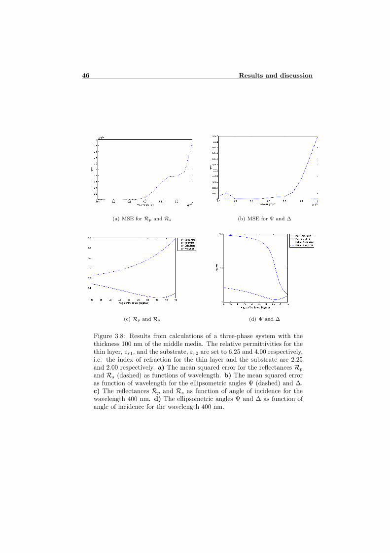
46 Results and discussion
(a) MSE for Rp and Rs (b) MSE for Ψ and ∆
(c) Rp and Rs (d) Ψ and ∆
Figure 3.8: Results from calculations of a three-phase system with thethickness 100 nm of the middle media. The relative permittivities for thethin layer, εr1, and the substrate, εr2 are set to 6.25 and 4.00 respectively,i.e. the index of refraction for the thin layer and the substrate are 2.25and 2.00 respectively. a) The mean squared error for the reflectances Rp
and Rs (dashed) as functions of wavelength. b) The mean squared erroras function of wavelength for the ellipsometric angles Ψ (dashed) and ∆.c) The reflectances Rp and Rs as function of angle of incidence for thewavelength 400 nm. d) The ellipsometric angles Ψ and ∆ as function ofangle of incidence for the wavelength 400 nm.

3.3 Three-phase system 47
εr1 εr2 Ψ ∆ Rp Rs
2.25 2.25 4.98e-5 8.19e-4 2.83e-8 8.86e-74.00 2.25 9.89e-5 6.07e-3 1.01e-8 2.73e-66.25 2.25 7.30e-4 2.58e-2 7.68e-8 4.24e-69.00 2.25 2.10e-3 6.21e-2 7.31e-7 6.75e-62.25 4.00 7.21e-5 2.16e-3 4.68e-8 7.71e-74.00 4.00 6.62e-5 1.84e-3 8.53e-9 2.12e-66.25 4.00 1.61e-4 1.32e-2 1.66e-8 3.40e-69.00 4.00 5.27e-2 9.02e-4 3.09e-7 5.09e-62.25 6.25 2.57e-4 2.34e-3 1.23e-7 1.33e-64.00 6.25 1.42e-4 4.53e-3 3.93e-8 2.49e-66.25 6.25 6.21e-5 1.55e-2 4.57e-8 4.00e-69.00 6.25 4.39e-4 4.39e-2 1.33e-7 5.54e-62.25 9.00 5.85e-4 1.40e-2 2.68e-7 1.71e-64.00 9.00 8.23e-4 1.20e-2 9.36e-8 2.65e-66.25 9.00 3.79e-4 1.33e-2 8.95e-8 4.09e-69.00 9.00 1.04e-4 1.74e-2 1.15e-7 5.24e-6
avg. 3.67e-3 1.47e-2 1.33e-7 3.31e-6
Table 3.6: The mean squared error for three-phase systems with the thick-ness of the middle media set to 1000 nm and with varying relative permit-tivities. The relative permittivity of the thin layer and for the substrateare denoted εr1 and εr2, respectively. The details of the marked simulationserie is shown in a separate figure.

48 Results and discussion
(a) MSE for Rp and Rs (b) MSE for Ψ and ∆
(c) Rp and Rs (d) Ψ and ∆
Figure 3.9: Results from calculations of a three-phase system with thethickness 1000 nm of the middle media. The relative permittivities for thethin layer εr1 and the substrate εr2 are set to 6.25 and 4.00 respectively,i.e. the index of refraction for the thin layer and the substrate are 2.25and 2.00 respectively. a) The mean squared error for the reflectances Rp
and Rs (dashed) as functions of wavelength. b) The mean squared erroras function of wavelength for the ellipsometric angles Ψ (dashed) and ∆.c) The reflectances Rp and Rs as function of angle of incidence for thewavelength 400 nm. d) The ellipsometric angles Ψ and ∆ as function ofangle of incidence for the wavelength 400 nm.

3.3 Three-phase system 49
Max size. Ψ ∆ Rp Rs
25 nm 1.61e-4 1.32e-2 1.66e-8 3.40e-620 nm 5.97e-5 4.56e-3 5.17e-9 3.31e-6
Table 3.7: The mean squared error for three-phase systems with the thick-ness of the middle media set to 1000 nm and with varying relative permit-tivities. The relative permittivities were 6.25 for the thin layer, εr1, and4.00 for the substrate, εr2. The details from both these simulation seriesare shown in separate figures.
From these Tables (3.4, 3.5 and 3.6) and figures (3.7 3.8 and 3.9) it is seen thatthe accuracy for these three-phase simulations are rather good. The MSE tendsto increase towards longer wavelengths but remains on a reasonable level for thisapplication tool. In Fig. 3.9(b) there are indications of a rather strong increase inthe difference between the calculated and the analytical values of the ellipsometricangle ∆ for the shorter wavelength, especially the end-value 400 nm. This couldbe an effect of that the density of the mesh is too small, i.e. to large elements areused. A reduction of the maximum allowed size of the elements from 25 to 20 nmgave the results shown in Table 3.7 and Fig. 3.10. When comparing Fig. 3.9(b)and 3.10(b) it is seen that the MSE for ∆ at the end-value wavelength 400 nm hasdecreased from above 0.1 to below 0.02 whereas the value for the other end-valueof the wavelength, 1000 nm, is unchanged at a value around 0.02.
A decrease of the maximum allowed size of the elements from 25 to 20 nm in-creases the number of elements from almost 35 000 for this model to about 55 000elements. This represents an increase in degrees of freedom from almost 140 000to about 220 000, which makes the requirements of available memory and compu-tational time significantly larger.
Table 3.8 and Fig. 3.11 presents data from simulation series of a model with anabsorbing substrate. To reduce the number of simulations the thickness 100 nmwere chosen for all series. As seen the accuracy is not significantly lower than forthe non-absorbing series, and the result may be seen as acceptable.
In Table 3.9 the result from similar simulation series done with an absorbinglayer and a non-absorbing substrate are presented. The results here are overallgood and with a strong absorption in the layer it can be seen that the change ofsubstrate has a limited effect on the accuracy.

50 Results and discussion
(a) MSE for Rp and Rs (b) MSE for Ψ and ∆
(c) Rp and Rs (d) Ψ and ∆
Figure 3.10: Results from calculations of a three-phase system with themaximum allowed size of the elements in the mesh reduced from 25 nmto 20 nm. The thickness is 1000 nm of the middle media and the relativepermittivities for the thin layer εr1 and the substrate εr2 are, as before,set to 6.25 and 4.00 respectively. a) The mean squared error for thereflectances Rp and Rs (dashed) as functions of wavelength. b) Themean squared error as function of wavelength for the ellipsometric anglesΨ (dashed) and ∆. c) The reflectances Rp and Rs as function of angle ofincidence for the wavelength 400 nm. d) The ellipsometric angles Ψ and∆ as function of angle of incidence for the wavelength 400 nm.

3.3 Three-phase system 51
εr1 εr2 Ψ ∆ Rp Rs
2.25 4.00- 2.00i 1.13e-4 4.38e-4 9.60e-8 5.44e-74.00 4.00- 2.00i 6.44e-5 9.16e-4 2.45e-8 1.33e-66.25 4.00- 2.00i 4.27e-5 3.87e-3 7.75e-9 4.02e-69.00 4.00- 2.00i 1.31e-4 6.64e-3 3.21e-8 5.71e-62.25 4.00-10.00i 5.54e-4 1.57e-3 7.47e-7 1.24e-64.00 4.00-10.00i 3.40e-5 4.40e-4 3.73e-7 2.88e-76.25 4.00-10.00i 3.41e-4 2.55e-3 7.00e-8 2.95e-69.00 4.00-10.00i 5.83e-4 1.33e-2 6.63e-8 5.91e-6
avg. 2.33e-4 3.72e-3 1.77e-7 2.75e-6
Table 3.8: The mean squared error for three-phase systems with the thick-ness of the middle media set to 100 nm and with varying real valued rela-tive permittivity of the thin layer εr1 and with a complex valued relativepermittivity εr2 of the substrate. The details of the marked simulationserie is shown in a separate figure.
εr1 εr2 Ψ ∆ Rp Rs
4.00- 2.00i 2.25 6.79e-5 2.59e-3 7.45e-9 3.42e-64.00- 2.00i 4.00 9.17e-5 2.26e-3 1.07e-8 2.94e-64.00- 2.00i 6.25 1.23e-4 2.02e-3 1.87e-8 2.64e-64.00- 2.00i 9.00 1.63e-4 1.64e-4 3.20e-8 2.44e-64.00-10.00i 2.25 3.77e-4 4.96e-3 6.40e-8 5.51e-64.00-10.00i 4.00 3.71e-4 4.85e-3 6.30e-8 5.40e-64.00-10.00i 6.25 3.64e-4 4.75e-3 6.19e-8 5.31e-64.00-10.00i 9.00 3.57e-4 4.65e-3 6.09e-8 5.24e-6
avg. 2.39e-4 3.28e-3 3.98e-8 4.11e-6
Table 3.9: The mean squared error for three-phase systems with the thick-ness of the middle media set to 100 nm and with two different complexvalued relative permittivities of the thin layer εr1 and with varying valuesof the relative permittivity of the substrate εr2.

52 Results and discussion
(a) MSE for Rp and Rs (b) MSE for Ψ and ∆
(c) Rp and Rs (d) Ψ and ∆
Figure 3.11: Results from calculations of a three-phase system with com-plex relative permittivity of the substrate. The thickness of the thin layeris 100 nm and the relative permittivity εr1 is set to 6.25. The substratecomplex relative permittivity εr2 is set to 4.00 − 10.00i, i.e. the complexindex of refraction for the substrate is N2 ≈ 2.72 − 1.84i whereas for thethin layer N1 = 2.50. a) The mean squared error for the reflectances Rp
and Rs (dashed) as functions of wavelength. b) The mean squared erroras function of wavelength for the ellipsometric angles Ψ (dashed) and ∆.c) The reflectances Rp and Rs as function of angle of incidence for thewavelength 900 nm. d) The ellipsometric angles Ψ and ∆ as function ofangle of incidence for the wavelength 900 nm.

3.4 Four-phase system 53
3.4 Four-phase system
3.4.1 The model
Figure 3.12: The geometry for the four-phase system. The upper andlower domains are perfectly matched layers, which approximates infiniteextension of the two outer phases in vertical direction. The two middledomains are thin layers of different medias. The left and right bound-aries are connected with periodic boundary conditions which results in aninfinite extension of the model in the horizontal direction. The incidentwave is introduced on the upper boundary of the upper thin layer withthe scattered-field formulation. The color (grayscale in printed version)represents the instantaneous electric field, where the illustrated field inthe two upper domains is the reflected field and in the four lower domainsthe transmitted. The wave fronts of the incident field are indicated withcontour lines. The width of the model used in this application tool isillustrated with the two vertical lines in the middle of the figure. In thissimulation the angle of incidence is 75 degrees with the thicknesses 500 nmof the two thin layers and the relative permittivities for the layers and thesubstrate set to 9.00, 4.00 and 9.00, respectively.
The last model only using homogenous thin layers is the four-phase model,shown in Fig. 3.12, i.e. reflections from a pair of thin layers on a substrate. As inthe previous models, PML and PBC are used to obtain infinite extensions and thelayers are introduced between the ambient media and the substrate. The boundarywhich introduces the incident wave is the upper boundary of the upper thin layer,

54 Results and discussion
εr1 εr2 εr3 Ψ ∆ Rp Rs
4.00 6.25 9.00 2.13e-4 5.14e-3 4.38e-8 5.56e-64.00 9.00 6.25 5.55e-5 5.83e-3 2.81e-8 4.69e-66.25 4.00 9.00 2.46e-4 5.59e-3 3.84e-8 5.40e-66.25 9.00 4.00 7.41e-5 1.99e-3 3.22e-8 3.81e-69.00 4.00 6.25 6.89e-5 3.58e-3 2.04e-8 6.06e-69.00 6.25 4.00 7.41e-5 1.99e-3 3.22e-8 4.81e-6
avg. 1.22e-4 4.02e-3 3.25e-8 5.06e-6
Table 3.10: Mean squared error for the four-phase system with the thick-ness 10 nm of both layers. The upper layer has the relative permittivityεr1, the bottom layer εr2 and the substrate εr3.
i.e. the boundary of the scattering media. These two thin layers introduces four(six) new parameters which defines each model, the relative permittivities (andrelative permeabilities) and the thicknesses of the two layers. The permittivitieschosen for this verification process are 4.00, 6.25 and 9.00, i.e. the indexes ofrefraction 2.00, 2.50 and 3.00, and the thicknesses are 10, 100 and 1000 nm. In thecase of absorbing medias is the imaginary part of the complex relative permittivityset to 10i.
3.4.2 Calculation resultsThe data from simulation series done with the layers of equal thickness, 10, 100and 1000 nm, are shown in Table 3.10, 3.11 and 3.12 respectively. The averageresult shows that the accuracy decreases slightly with the increasing size, espe-cially for the ellipsometric angle ∆. Figure 3.13 presents the detailed result fromthe simulation on a model with the relative permittivities εr1, εr2 and εr3 set to4.00, 6.25 and 9.00, respectively. From Fig. 3.13(b) it is seen that the major partof the inaccuracy originates from simulations with the wavelength 450 nm. Thevariation of ∆ as function of angle of incidence for this wavelength is shown inFig. 3.14. From this figure it is seen that the deviation between the calculatedvalues and the analytical expressions are increased around the angles of incidence65 to 70 degrees, i.e. close to the steep slope, otherwise the fit is rather good.
The accuracy for the model with a thin layer, 10 nm, on top of a thicker layer,100 nm, is presented in Table 3.13. The result here does not differ much fromthe previously presented models and as can bee seen in Fig. 3.15 the major partof inaccuracy is due to a too sparse mesh for the shortest wavelength, 400 nm,according to previous discussions.
In Table 3.14, where the result from models with increasing absorption is pre-sented, the accuracy here is on a similar level. As usual the inaccuracy is highestfor the ellipsometric angle ∆, but it is still acceptable.

3.4 Four-phase system 55
εr1 εr2 εr3 Ψ ∆ Rp Rs
4.00 6.25 9.00 3.84e-5 3.40e-3 2.24e-8 1.91e-64.00 9.00 6.25 2.01e-4 9.34e-4 1.43e-7 8.15e-76.25 4.00 9.00 4.03e-4 7.22e-3 1.94e-8 5.87e-66.25 9.00 4.00 1.00e-4 1.77e-3 5.10e-8 1.83e-69.00 4.00 6.25 2.90e-4 8.21e-3 2.51e-8 6.39e-69.00 6.25 4.00 5.92e-5 5.06e-3 8.73e-9 3.94e-6
avg. 1.82e-4 4.43e-3 4.49e-8 3.38e-6
Table 3.11: Mean squared error for the four-phase system with the thick-ness 100 nm of both layers. The upper layer has the relative permittivityεr1, the bottom layer εr2 and the substrate εr3.
εr1 εr2 εr3 Ψ ∆ Rp Rs
4.00 6.25 9.00 8.23e-4 5.01e-2 3.56e-8 2.81e-64.00 9.00 6.25 5.52e-3 1.63e-1 1.18e-8 3.07e-66.25 4.00 9.00 1.53e-3 6.11e-2 1.59e-7 5.31e-66.25 9.00 4.00 5.26e-3 3.48e-1 6.54e-7 7.29e-69.00 4.00 6.25 1.42e-3 4.80e-2 7.62e-7 6.86e-69.00 6.25 4.00 1.28e-3 9.52e-1 4.25e-7 6.06e-6
avg. 2.64e-3 2.70e-1 3.41e-7 5.23e-6
Table 3.12: Mean squared error for the four-phase system with the thick-ness 1000 nm of both layers. The upper layer has the relative permittivityεr1, the bottom layer εr2 and the substrate εr3. The details of the markedsimulation serie is shown in a separate figure.
εr1 εr2 εr3 Ψ ∆ Rp Rs
4.00 6.25 9.00 4.01e-4 1.17e-2 2.42e-7 5.60e-64.00 9.00 6.25 7.14e-4 9.51e-2 3.51e-7 7.26e-66.25 4.00 9.00 6.49e-4 4.37e-2 2.46e-7 4.19e-66.25 9.00 4.00 1.34e-3 8.31e-2 6.53e-7 8.10e-69.00 4.00 6.25 1.86e-4 4.11e-3 1.58e-7 4.37e-69.00 6.25 4.00 2.06e-4 2.06e-2 2.28e-7 5.89e-6
avg. 5.83e-4 4.31e-2 3.13e-7 5.90e-6
Table 3.13: Mean squared error for the four-phase system with the thick-ness 10 nm and 1000 nm of the upper and the lower layer, respectively.The upper layer has the relative permittivity εr1, the bottom layer εr2
and the substrate εr3. The details of the marked simulation serie is shownin a separate figure.

56 Results and discussion
(a) MSE for Rp and Rs (b) MSE for Ψ and ∆
(c) Rp and Rs (d) Ψ and ∆
Figure 3.13: The results from calculations on a four-phase system withboth thicknesses set to 1000 nm, the relative permittivities in the upperand the lower layer are set to 4.00 and 6.25 respectively. The relativepermittivity in the substrate is 9.00. a) The mean squared error of thereflectances Rp and Rs (dashed). b) The mean squared error as functionof wavelength for the ellipsometric angles Ψ (dashed) and ∆. c) Thereflectances Rp and Rs as function of angle of incidence for the wavelength400 nm. d) The ellipsometric angles Ψ and ∆ as function of angle ofincidence for the wavelength 400 nm.

3.4 Four-phase system 57
Figure 3.14: The variations of the ellipsometric angle ∆ for a four-phasesystem with both thicknesses of the thin layers set to 1000 nm, and therelative permittivities for the upper layer, lower layer and the substrateset to 4.00, 6.25 and 9.00 respectively. The wavelength for this calculationwas 450 nm.
εr1 εr2 εr3 Ψ ∆ Rp Rs
4.00 6.25 9.00 4.03e-4 7.22e-3 1.94e-8 5.87e-64.00 6.25 9.00-10.00i 1.08e-4 4.80e-3 2.34e-8 3.65e-64.00 6.25-10.00i 9.00-10.00i 3.16e-5 5.94e-4 3.56e-7 2.64e-7
4.00-10.00i 6.25-10.00i 9.00-10.00i 3.17e-4 4.80e-3 3.34e-8 5.29e-6avg. 2.15e-4 4.35e-3 1.08e-7 3.77e-6
Table 3.14: Mean squared error for the absorbing four-phase system withthe thickness 100 nm of both the upper and the lower layer. The complexrelative permittivity for the upper and lower layer, εr1 and εr2 as well asfor the substrate εr3 are gradually increased.

58 Results and discussion
(a) MSE for Rp and Rs (b) MSE for Ψ and ∆
(c) Rp and Rs (d) Ψ and ∆
Figure 3.15: The results from calculations on a four-phase system with thethickness of the upper layer set to 10 nm and the thickness of the lowerlayer set to 1000 nm. The relative permittivities in the upper and thelower layer are set to 9.00 and 6.25 respectively. The relative permittivityin the substrate is 4.00. a) The mean squared error of the reflectances Rp
and Rs (dashed). b) The mean squared error as function of wavelengthfor the ellipsometric angles Ψ (dashed) and ∆. c) The reflectances Rp
and Rs as function of angle of incidence for the wavelength 400 nm. d)The ellipsometric angles Ψ and ∆ as function of angle of incidence for thewavelength 400 nm.
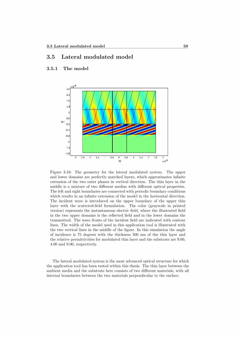
3.5 Lateral modulated model 59
3.5 Lateral modulated model
3.5.1 The model
Figure 3.16: The geometry for the lateral modulated system. The upperand lower domains are perfectly matched layers, which approximates infiniteextension of the two outer phases in vertical direction. The thin layer in themiddle is a mixture of two different medias with different optical properties.The left and right boundaries are connected with periodic boundary conditionswhich results in an infinite extension of the model in the horizontal direction.The incident wave is introduced on the upper boundary of the upper thinlayer with the scattered-field formulation. The color (grayscale in printedversion) represents the instantaneous electric field, where the illustrated fieldin the two upper domains is the reflected field and in the lower domains thetransmitted. The wave fronts of the incident field are indicated with contourlines. The width of the model used in this application tool is illustrated withthe two vertical lines in the middle of the figure. In this simulation the angleof incidence is 75 degrees with the thickness 500 nm of the thin layer andthe relative permittivities for modulated thin layer and the substrate are 9.00,4.00 and 9.00, respectively.
The lateral modulated system is the most advanced optical structure for whichthe application tool has been tested within this thesis. The thin layer between theambient media and the substrate here consists of two different materials, with allinternal boundaries between the two materials perpendicular to the surface.

60 Results and discussion
Figure 3.17: The intensity of the s-polarized part of the reflected wave.The model has the relative permittivities εr1a, εr1b and εr2 set to 9.00,6.25 and 4.00, respectively. The thickness of the modulated layer is 100 nmand the width of the materials placed next to each other are 100 nm. Theangle of incidence is 75 degrees and the wavelength 500 nm. The color(grayscale in printed version) show the intensity of the s-component of thereflected wave. Since the intensity of the incident wave is set to unity, thisrepresents the reflectance Rs. As seen the intensity is homogenous a fewhundred nm above the surface, whereas variations are present close to thesurface.
3.5.2 Calculation resultsFor simplicity the two materials were considered to be of equal width, and onlyone thickness of the layer were considered, 100 nm. The relative permittivities arevaried between 4.00, 6.25 and 9.00, as in the case of the four-phase system. Theresult from these simulation series are presented in Table 3.15. Since the width ofthe two materials in the modulated layer are equal, the systems where εr1a andεr1b are reversed should be equal, and thereby only one of them are simulated inthis verification process.
As seen in Table 3.15 the accuracy for this lateral modulated model is signifi-cantly lower than for the previous models. Figure 3.18 presents the details fromthe simulation with the relative permittivities set to 6.25 and 4.00 for the two ma-terials in the thin layer, and 9.00 for the substrate. As seen, there are no specificwavelengths that lowers the accuracy for all parameters. Figure 3.18(c) shows thatthere is a slight bias between the calculated value and the analytical expressions.
In Fig. 3.17 the intensity of the s-component of the reflected field is shown ina model with the relative permittivities εr1a, εr1b and εr2 set to 9.00, 6.25 and

3.5 Lateral modulated model 61
εr1a εr1b εr2 Ψ ∆ Rp Rs
6.25 9.00 4.00 4.76e0 1.51e2 6.80e-5 2.45e-44.00 9.00 6.25 2.79e1 1.65e3 8.18e-4 1.27e-34.00 6.25 9.00 1.99e0 7.85e1 9.39e-5 6.36e-4
avg. 3.97e1 8.53e2 4.00e-4 2.00e-2
Table 3.15: Mean squared error for the lateral modulated system withthe thickness 100 nm of the modulated layer. The width of the modula-tion medias are 100 nm each and their relative permittivity are εr1a andεr1b. The substrate relative permittivity is εr2. The details of the markedsimulation serie is shown in a separate figure.
4.00, respectively. The thickness of the thin layer is set to 100 nm, and the widthof the materials used in the modulated layer are 100 nm. The angle of incidence is75 degrees and the wavelength 500 nm. The intensity is homogenous from about100 nm above the thin layer, whereas variations depending on the lateral structureof the thin layer can be observed close to the surface.

62 Results and discussion
(a) MSE for Rp and Rs (b) MSE for Ψ and ∆
(c) Rp and Rs (d) Ψ and ∆
Figure 3.18: Results from calculations of the lateral modulated systemwith equal width, 100 nm, of the medias in the modulated layer. Thethickness of the layer is 100 nm. The relative permittivities for the ma-terials in the layer, εr1a and εr1b are set to 4.00 and 6.25 respectively.The relative permittivity of the substrate εr2 is set to 9.00. a) The meansquared error for the reflectances Rp and Rs (dashed) as functions ofwavelength. b) The mean squared error as function of wavelength for theellipsometric angles Ψ (dashed) and ∆. c) The reflectances Rp and Rs asfunction of angle of incidence for the wavelength 400 nm. d) The ellipso-metric angles Ψ and ∆ as function of angle of incidence for the wavelength400 nm.

3.6 Summary 63
3.6 SummaryIn this chapter the result from the calculations has been displayed and the differ-ences between the result and the analytical values are discussed. The next chapterwill conclude the work presented in this chapter and present the possibilities tofurther develop the tool in the future.

64 Results and discussion

Chapter 4
Conclusions and future work
This chapter concludes the current state of the developed application tool. Thepossibilities and weaknesses that have been found during the process of develop-ment will be pointed out. The future possibilities for this application tool areglanced at and possible enhancements for the tool will be mentioned, as well asnew structures that can be simulated.
4.1 ConclusionsThe verification process has shown that the application tool have a good accu-racy for all tested models with flat homogenous interfaces. Absorbing medias doesnot significantly decrease the accuracy. The accuracy tends to decrease for longerwavelengths, which might be an effect of too small model sizes. For calculationswith main focus in wavelengths of 1000 nm or above a larger model may be rec-ommendable. This will unfortunately force the user to avoid simulations in theshorter wavelength regions, around 400 nm, in the same model, since the needfor a high density of the mesh will make the model too memory demanding foran ordinary desktop computer. This could to some extent be compensated witha flexible design of the size of the model, i.e. model size would change with thewavelength. Though, when introducing complex surface structures in the model,this might become challenging to realize. Another possible solution would be tocreate a few models with static size optimized for different wavelength regions.
For the lateral modulated model the inaccuracy is more pronounced. With thecurrent setup of this model, the result from the lateral model unfortunately is notto be trusted.
4.2 Future workThe future work may be divided into two different groups, enhancements of thetechnique used and new structures to model.
65

66 Conclusions and future work
4.2.1 Enhanced techniquesIncreased range of angles of incidence
The current application tool has only been verified for angles of incidence up to75 degrees, since within spectroscopic ellipsometry these are the most commonlyused angles. Some tests, not documented in this thesis, have been made on anglescloser to 90 degrees, and some decreased accuracy were obtained. These limits arestill to be documented and mapped out.
Presentation of Delta
For convenience reasons the ellipsometric angle ∆ is plotted only in the range[0, 180]. This is done to avoid misleading jumps of 360 degrees, but instead thereare unwanted mirroring effects when the phase shift passed 180 degrees. Thisproblem should be possible to solve, and thereby obtain a plot of ∆ in the range[0, 360[.
Far-field-approximations
A way to perform the far-field approximation could be developed to guaranteethat no near-field effects are observed when extracting the result. This will alsoin a better way approximate the experimental ellipsometry setup.
Optical conductivity
Another way to describe the optical properties of materials is the optical conduc-tivity σ. This is supported in Multiphysics and should be convenient to implementin the application tool.
Ellipsometric setup
It would be possible to create a graphical user interface focused on resemble anellipsometry program, and thereby making this tool more user friendly for usetogether with ellipsometry.
4.2.2 More advanced modelingAmbient media
The application tool is implemented in a way that only allows for air, i.e. emptyspace, as ambient media. This limits the possibilities to use the tool for someother application areas, for example total internal reflection.
Wavelength dependent material parameters
This application tool uses static values for εr and µ even though these parametersusually vary with wavelength. This should be implemented in such a way that

4.3 Summary 67
these properties can be defined by analytical expressions or by tabulated values,for which the wanted values may be interpolated.
More advanced structures
The first step is to improve the accuracy of the laterally modulated model, thereafter a natural step would be to replace one of the materials with empty space,thereby creating a simple form of surface structures on the surface. These surfacestructures may then be transformed into pillars, which could be compared with themetamaterials created by Grigorenko et al. [5], or they could be designed like the"Christmas tree" structure found on the wings of the butterfly Morpho rhetenor.
3D models
Some structures can not be approximated with a two-dimensional mode, and afull three-dimensional model must be used. This will require a lot of more com-putational power, which will not be possible to perform on a ordinary desktopcomputer. Such a change of model would require a rebuilding of the applicationtool, since the modules used in Multiphysics will have to be changed, which forexample leads to different ways to describe the electromagnetic fields.
Optimization of computational time
Since the different parts of the simulation sets are independent of each other, itcould be possible to parallelize the calculations and thereby enable usage of clus-tered computational environments, which would drastically increase the possiblesize of the models and also reduce the computational time. The work order of theapplication tool could also be altered to minimize the memory usage for calcula-tion on an ordinary desktop computer, which could enable simulations of largermodels.
4.3 SummaryThis chapter has presented a conclusion of the work done within this thesis, anddisplayed some of the possibilities for improvements that can be made.

68 Conclusions and future work

Bibliography
[1] J. C. Maxwell, A treatise on electricity and magnetism. Oxford: ClaredonPress, 1873.
[2] J. B. Pendry, A. J. Holden, W. J. Stewart, and I. Youngs, “Extremely lowfrequency plasmons in metallic mesostructures,” Physical Review Letters,vol. 76, no. 25, pp. 4773–4776, 1996.
[3] J. B. Pendry, A. J. Holden, D. J. Robbins, and W. J. Stewart, “Mag-netism from conductors and enhanced nonlinear phenomena,” IEEE Trans.Microwave Theory Tech., vol. 47, no. 11, pp. 2075–2084, 1999.
[4] D. R. Smith, W. J. Padilla, D. C. Vier, S. C. Nemat-Nasser, and S. Schultz,“Composite medium with simultaneously negative permeability and permit-tivity,” Physical Review Letters, vol. 84, no. 18, pp. 4184–4187, 2000.
[5] A. N. Grigorenko, A. K. Geim, H. F. Gleeson, Y. Zhang, A. A. Firsov, I. Y.Khrushchev, and J. Petrovic, “Nanofabricated media with negative perme-ability at visible frequencies,” Nature, vol. 438, pp. 335–338, November 2005.10.1038/nature04242.
[6] V. P. Drachev, W. Cai, U. Chettiar, H. K. Yuan, A. K. Sarychev, A. V.Kildishev, G. Klimeck, and V. M. Shalaev, “Experimental verification of anoptical negative-index material,” Laser Phys. Lett., vol. 3, no. 1, pp. 49–55,2006.
[7] V. M. Shalaev, W. Cai, U. Chettiar, H.-K. Yuan, A. K. Sarychev, V. P.Drachev, and A. V. Kildishev, “Negative index of refraction in optical meta-materials,” Optics Letters, 2005.
[8] P. Vukusic and J. Sambles, “Photonic structures in biology,” Nature, vol. 424,pp. 852–855, 2003.
[9] K.-M. Chae, H.-H. Lee, S.-Y. Yim, and S.-H. Park, “Evolution of electromag-netic interference through nano-metallic double-slit,” Optics Express, vol. 12,pp. 2870–2879, June 2004.
[10] J. W. Goodman, Introduction to Fourier Optics. McGraw-Hill Inc., sec-ond ed., 1996.
69

70 Bibliography
[11] J. A. Stratton, Electromagnetic Theory. McGraw-Hill, 1941.
[12] J. Jin, The Finite Element Method in Electromagnetics. Wiley-IEEE Press,second ed., 2002.
[13] J.-P. Berenger, “A perfectly matched layer for the absorption of electromag-netic waves,” J. Comput. Phys., vol. 114, no. 2, pp. 185–200, 1994.
[14] S. A. Cummer, “Perfectly matched layer behavior in negative refractive indexmaterials,” Antennas and Wireless Propagation Letters, vol. 3, pp. 172–175,2004.
[15] J. D’Angelo and I. D. Mayergoyz, “Three dimensional rf scattering by thefinite element method,” Magnetics, IEEE Transactions on, vol. 27, pp. 3827–3832, 1991.
[16] V. G. Veselago, “The electrodynamics of substances with simultaneously neg-ative values of permittivity and permeability.,” Sov. Phys. Usp., vol. 10,pp. 509–514, 1968.
[17] R. A. Shelby, D. R. Smith, S. C. Nemat-Nasser, and S. Schultz, “Microwavetransmission through a two-dimensional, isotropic, left-handed metamate-rial,” Applied Physics Letters, vol. 78, no. 4, pp. 489–491, 2001.
[18] J. Zhou, T. Koschny, M. Kafesaki, E. N. Economou, J. B. Pendry, and C. M.Soukoulis, “Saturation of the magnetic response of split-ring resonators atoptical frequencies,” Physical Review Letters, vol. 95, no. 22, p. 223902, 2005.
[19] S. Linden, C. Enkrich, M. Wegener, J. Zhou, T. Koschny, and C. M. Soukoulis,“Magnetic Response of Metamaterials at 100 Terahertz,” Science, vol. 306,no. 5700, pp. 1351–1353, 2004.
[20] A. Ishikawa, T. Tanaka, and S. Kawata, “Negative magnetic permeability inthe visible light region,” Physical Review Letters, vol. 95, no. 23, p. 237401,2005.
[21] J. B. Pendry, “Negative refraction makes a perfect lens,” Physical ReviewLetters, vol. 85, no. 18, pp. 3966–3969, 2000.
[22] D. R. Smith, “How to Build a Superlens,” Science, vol. 308, no. 5721, pp. 502–503, 2005.

Appendix A
Appendix
A.1 Left Handed Materials
A.1.1 History
In 1968 Veselago [16] published a paper where he concluded that if a materialshould have both negative permittivity and negative permeability in the samefrequency region it would have to have a negative index of refraction to obtaincausality, i.e. the negative root to the square root in eq. 2.13 would have to beselected. Veselago predicted that such material would have contraintuitive prop-erties, for example would the incident and refracted wave be on the same sideof the surface normal after refraction at an interface, the Doppler effect wouldbe inversed and the propagation direction would be reversed with respect to thedirection of the energy flow.
It is quite common to have materials with a negative real part of the permittivity,ε′. Materials with a negative real part of the permeability µ′ are less common,but still rather easy to find. Examples of those are resonant ferromagnetic orantiferromagnetic systems. The resonances are at much lower frequencies and theresonances do usually tail off toward the THz to infrared region. Consequentlyare there no naturally occurring materials which have both a negative permittivityand a negative permeability in the same frequency, since these resonant phenome-nas do not occur at the same frequency-regions. At least there are no such naturalmaterials known today.
By introducing the thin wires and the Split Ring Resonant as described in 2.1.4 onpage 8 it is possible to create metamaterials with negative index of refraction infinite frequency regions. The first experiments were done by Smith et al. [4] usinga one-dimensional medium (i.e. one direction of incidence and polarization), con-sisting of unit cells containing one SRR and one conducting post each. By usingtransmission measurements, their experiments verified that these two structuresintroduced a negative permeability and a negative permittivity which introduced
71

72 Appendix
a pass band in the previously forbidden, opaque, frequency region.
The next step was performed by Shelby et al. [17] when they constructed a two di-mensional sample with the frequency region of negative refraction at about 10GHz.The metamaterial they used consisted of thin wires and SRRs embedded in fiberglass and with this prism-shaped metamaterial they calculated the index of refrac-tion for the metamaterial to be about −2.7 by using Snell’s law and measurementsof the refraction angle. This result was compared with a similar prism withoutthe thin wires and the SRRs, where a normal index of refraction were measured.
To be able to introduce similar types of metamaterials for use in the visible regime,it is necessary to create nano-sized structures with the same, or similar, propertiesas the thin wires and the SRRs. In frequency regions up to a few THz the mag-netic resonance frequency scales reciprocally with the size of the SRR. At higherfrequencies, this is unfortunately no longer true [18]. This means that the struc-tures have to be even smaller to achieve a magnetic response at visible frequencies.Since the ohmic losses increase with the decreased size of the structures, the visiblefrequencies seemed to be out of reach for the left hand materials. But Linden etal. [19] succeeded in creating a metamaterial with negative magnetic permeabilityat 85 THz (λ ≈ 3.5 µm). The size of the simplified single split-ring resonators(SSRR) they used were about 350x350 nm and the measured transmission spectragave more than 90 % transmission. This gave hope for that LHMs in the visiblefrequency could be possible. In late 2005, Ishikawa et al. [20] presented theoreticalcalculations indicating that SSRRs made of silver could exhibit a negative realpart of the permeability and still have a quite low absorption, which would furtherincrease the possibilities to create a LHM in the visible region.
At the same time Shalaev et al. [6, 7] did construct a double-periodic array of pairsof parallel gold nano rods. These rods were about 800x200 nm in size, and abovethe resonance frequency were circular currents induced in the pairs, which led to amagnetic field opposing the external magnetic field of the light. By interferometricmeasurements a negative index of refraction of about −0.3 were obtained at theinfrared wavelength λ = 1.5 µm. Unfortunately the imaginary part of the indexof refraction was large, but calculations showed that optimization of the systemcould create better impedance matching which would significantly decrease theimaginary part. Grigorenko et al. [5] published at the end of 2005 the result ofmeasurements, calculations and simulations of a metamaterial consisting of goldnanopillars placed in pairs. These pillars have a reduced number of resonance fre-quencies due to their simple geometry, and thereby a decreased absorption. Themedium exhibits a strong magnetic resonance at visible-light frequencies, includ-ing a band with negative permeability. The pillars had a radius of about 100 nmand were 80-90 nm high. A plasmon resonance observed for an individual pillarare shown to split into two resonances for a pillar pair. One of these are symmet-ric, i.e. the electrons will move in phase in the neighboring pillars and generatea dipole contribution to the permittivity. The other resonance is anti-symmetric,i.e. the electrons will move out of phase so that the oscillating dipoles cancel each

A.1 Left Handed Materials 73
other. The movement of the electrons will create a current loop, which will createa magnetic moment contributing to the permeability. These resonances were stud-ied by simulations of a pillar pair using the FEMLAB® software (Comsol® AB.).Although the pillar pairs exhibited negative real parts of both the permittivityand the permeability at the same frequency region, no negative refraction was ob-served due to the quite large imaginary part of the permeability. But the receivedproperties of the structure showed impedance matching to the environment at thefrequency for green light, leading to that the surface showed no reflection.
A.1.2 Application areasThere are several areas where left handed materials could be useful. Some arepresented here.
Superlens
One of the first discussed applications for left handed materials were the superlenspresented by J.B. Pendry [21]. With a normal lens, the resolution of the image cannever be greater than the wavelength, no matter how perfect the lens is or howlarge the aperture is. Pendry showed that a parallel-sided slab of LHM, preferablewith both εr and µr equal to −1, would act as a perfect lens by amplifying theevanescent wave, which normally decay in amplitude and not in phase. Therebywould the resolution limit at the wavelength be avoided. This amplification of theevanescent waves does not violate the energy conservation because they do nottransport energy, the evanescent waves do just store energy. The factor that willlimit the wavelength is in this case the quality of the slab. Pendry also suggestedthat for small systems, where all directions are smaller than the wavelength, thepermittivity and permeability will become uncoupled, and thereby it would beenough to have one of these negative to create a perfect lens. For example, itwould be possible to use a thin slab of silver as a lens. This type of superlenswith only negative permittivity was later created by D.R. Smith [22] and with thissilver slab they were able to create an image with enhanced resolution.
Anti-reflection coatings
As mentioned above is it possible to create materials which are impedance matchedwith the surrounding, and thereby eliminate reflections from the interface. Thematched impedance is only obtained in a limited wavelength region.
Magnetic resonance imaging
The possibility to induce magnetic response in materials at high frequencies canbe used within magnetic resonance imaging, where the applied field can be alteredby metamaterials.

74
List of Figures
2.1 p- and s-polarization . . . . . . . . . . . . . . . . . . . . . . . . . . 52.2 The Split Ring Resonant (SRR) . . . . . . . . . . . . . . . . . . . . 92.3 The three-phase system . . . . . . . . . . . . . . . . . . . . . . . . 122.4 The four-phase system . . . . . . . . . . . . . . . . . . . . . . . . . 132.5 The laterally modulated system . . . . . . . . . . . . . . . . . . . . 142.6 The macroscopic averages . . . . . . . . . . . . . . . . . . . . . . . 142.7 Reflected field from a double pillar structure . . . . . . . . . . . . . 16
3.1 The default geometry . . . . . . . . . . . . . . . . . . . . . . . . . 303.2 The two-phase model . . . . . . . . . . . . . . . . . . . . . . . . . . 353.3 The two-phase system . . . . . . . . . . . . . . . . . . . . . . . . . 373.4 The two-phase system . . . . . . . . . . . . . . . . . . . . . . . . . 383.5 The two-phase system, absorbing substrate . . . . . . . . . . . . . 403.6 The three-phase model . . . . . . . . . . . . . . . . . . . . . . . . . 423.7 The three-phase system, 10 nm . . . . . . . . . . . . . . . . . . . . 443.8 The three-phase system, 100 nm . . . . . . . . . . . . . . . . . . . 463.9 The three-phase system, 1000 nm . . . . . . . . . . . . . . . . . . . 483.10 The three-phase system, 1000 nm, denser mesh . . . . . . . . . . . 503.11 The three-phase system, absorbing substrate . . . . . . . . . . . . 523.12 The four-phase model . . . . . . . . . . . . . . . . . . . . . . . . . 533.13 The four-phase system, 1000 nm . . . . . . . . . . . . . . . . . . . 563.14 The four-phase system, 1000 nm, variations in Delta . . . . . . . . 573.15 The four-phase system, 10 nm and 1000 nm . . . . . . . . . . . . . 583.16 The lateral modulated model . . . . . . . . . . . . . . . . . . . . . 593.17 The lateral modulated system, intensity of the s-polarization . . . 603.18 The lateral modulated system, 100 nm . . . . . . . . . . . . . . . . 62

75
List of Tables
3.1 Structured and unstructured meshes . . . . . . . . . . . . . . . . . 313.2 MSE for two-phase systems . . . . . . . . . . . . . . . . . . . . . . 393.3 MSE for two-phase systems, absorbing substrate . . . . . . . . . . 413.4 MSE for three-phase systems, 10 nm . . . . . . . . . . . . . . . . . 433.5 MSE for three-phase systems, 100 nm . . . . . . . . . . . . . . . . 453.6 MSE for three-phase systems, 1000 nm . . . . . . . . . . . . . . . . 473.7 MSE for three-phase systems, 1000 nm, denser mesh . . . . . . . . 493.8 MSE for three-phase systems, 100 nm, absorbing substrate . . . . 513.9 MSE for three-phase systems, 100 nm, absorbing layer . . . . . . . 513.10 MSE for four-phase systems, 10 nm . . . . . . . . . . . . . . . . . . 543.11 MSE for four-phase systems, 100 nm . . . . . . . . . . . . . . . . . 553.12 MSE for four-phase systems, 1000 nm . . . . . . . . . . . . . . . . 553.13 MSE for four-phase systems, 10 resp. 1000 nm . . . . . . . . . . . 553.14 MSE for four phase systems, 100 nm, absorbing media. . . . . . . . 573.15 MSE for lateral modulated systems . . . . . . . . . . . . . . . . . . 61

76

UpphovsrättDetta dokument hålls tillgängligt på Internet — eller dess framtida ersättare —under 25 år från publiceringsdatum under förutsättning att inga extraordinäraomständigheter uppstår.
Tillgång till dokumentet innebär tillstånd för var och en att läsa, ladda ner,skriva ut enstaka kopior för enskilt bruk och att använda det oförändrat för icke-kommersiell forskning och för undervisning. Överföring av upphovsrätten vid ensenare tidpunkt kan inte upphäva detta tillstånd. All annan användning av doku-mentet kräver upphovsmannens medgivande. För att garantera äktheten, säker-heten och tillgängligheten finns det lösningar av teknisk och administrativ art.
Upphovsmannens ideella rätt innefattar rätt att bli nämnd som upphovsmani den omfattning som god sed kräver vid användning av dokumentet på ovan be-skrivna sätt samt skydd mot att dokumentet ändras eller presenteras i sådan formeller i sådant sammanhang som är kränkande för upphovsmannens litterära ellerkonstnärliga anseende eller egenart.
För ytterligare information om Linköping University Electronic Press se för-lagets hemsida http://www.ep.liu.se/
CopyrightThe publishers will keep this document online on the Internet — or its possi-ble replacement — for a period of 25 years from the date of publication barringexceptional circumstances.
The online availability of the document implies a permanent permission foranyone to read, to download, to print out single copies for your own use andto use it unchanged for any non-commercial research and educational purpose.Subsequent transfers of copyright cannot revoke this permission. All other uses ofthe document are conditional on the consent of the copyright owner. The publisherhas taken technical and administrative measures to assure authenticity, securityand accessibility.
According to intellectual property law the author has the right to be men-tioned when his/her work is accessed as described above and to be protectedagainst infringement.
For additional information about the Linköping University Electronic Pressand its procedures for publication and for assurance of document integrity, pleaserefer to its www home page: http://www.ep.liu.se/
© Henrik Wiklund