department of information engineering master thesis in ict...
TRANSCRIPT

Università degli Studi di Padova
Department of Information Engineering
Master thesis in ICT for Internet and Multimedia
Design and Simulation of Forward-biasedCoupling Modulation Ring Modulators
Master candidate Supervisor
Tommaso Pento Luca Palmieri
Co-supervisors
Jamshidi Kambiz
Sourav Dev
Academic Year 2018/2019, 9th December 2019

ii
Abstract
Silicon resonators are nowadays the subject of an intense research activ-ity since they can be employed in many different applications due to theirintrinsic advantages such as small footprint and low energy consumption.For instance, they are utilized in optical networks as multiplexers (MUX)and demultiplexers (DEMUX), proving to be extremely useful in the caseof Wavelength-Division Multiplexing (WDM) or Dense Wavelength-DivisionMultiplexing (DWDM) modulation, a technique used to increase the datarate of a given network. They are also suitable as optical modulators whenexposed to a varying electric field because of different physical phenomena,such as Kerr effect or Plasma Dispersion Effect (PDE). Furthermore, theyhave also proven useful for sensing purposes, being extremely sensitive tochanges in the environment, such as temperature or physical compositionof the device. In this thesis work, the performance of a ring modulator isevaluated with simulation software such as MATLAB and Lumerical. Thephysical properties are optimized in order to obtain the best results in termsof modulation efficiency, energy consumption and footprint.

iv

Contents
1 Introduction 11.1 Motivation . . . . . . . . . . . . . . . . . . . . . . . . . . . . . 11.2 Literature Review . . . . . . . . . . . . . . . . . . . . . . . . . 21.3 Contribution . . . . . . . . . . . . . . . . . . . . . . . . . . . . 41.4 Thesis Outline . . . . . . . . . . . . . . . . . . . . . . . . . . . 5
2 Fundamentals 72.1 Maxwell’s Equations . . . . . . . . . . . . . . . . . . . . . . . 7
2.1.1 Definition . . . . . . . . . . . . . . . . . . . . . . . . . 72.1.2 Complex vector representation . . . . . . . . . . . . . . 10
2.2 Losses . . . . . . . . . . . . . . . . . . . . . . . . . . . . . . . 122.3 Power . . . . . . . . . . . . . . . . . . . . . . . . . . . . . . . 132.4 Polarization . . . . . . . . . . . . . . . . . . . . . . . . . . . . 132.5 Wave packets . . . . . . . . . . . . . . . . . . . . . . . . . . . 152.6 Light pulses . . . . . . . . . . . . . . . . . . . . . . . . . . . . 172.7 Interference . . . . . . . . . . . . . . . . . . . . . . . . . . . . 182.8 Absorption and emission . . . . . . . . . . . . . . . . . . . . . 202.9 Scattering . . . . . . . . . . . . . . . . . . . . . . . . . . . . . 222.10 Nonlinear effects . . . . . . . . . . . . . . . . . . . . . . . . . 24
3 Propagation in Dielectric Media 293.1 Boundary conditions . . . . . . . . . . . . . . . . . . . . . . . 293.2 Snell’s Law . . . . . . . . . . . . . . . . . . . . . . . . . . . . 303.3 Waveguides . . . . . . . . . . . . . . . . . . . . . . . . . . . . 32
3.3.1 Introduction and materials . . . . . . . . . . . . . . . . 323.3.2 Optical modes . . . . . . . . . . . . . . . . . . . . . . . 33
3.4 Dispersion . . . . . . . . . . . . . . . . . . . . . . . . . . . . . 373.4.1 Modal dispersion . . . . . . . . . . . . . . . . . . . . . 383.4.2 Chromatic dispersion . . . . . . . . . . . . . . . . . . . 383.4.3 Polarization mode dispersion . . . . . . . . . . . . . . . 40
3.5 Coupling . . . . . . . . . . . . . . . . . . . . . . . . . . . . . . 41
v

vi CONTENTS
3.6 Attenuation . . . . . . . . . . . . . . . . . . . . . . . . . . . . 43
4 Modulators 454.1 Introduction . . . . . . . . . . . . . . . . . . . . . . . . . . . . 454.2 Mach Zehnder Modulator . . . . . . . . . . . . . . . . . . . . 474.3 Modulation techniques . . . . . . . . . . . . . . . . . . . . . . 48
4.3.1 Electro-absorption . . . . . . . . . . . . . . . . . . . . 484.3.2 Electro-refraction . . . . . . . . . . . . . . . . . . . . . 494.3.3 Plasma dispersion effect . . . . . . . . . . . . . . . . . 504.3.4 Thermo-optic effect . . . . . . . . . . . . . . . . . . . . 51
4.4 Parameters . . . . . . . . . . . . . . . . . . . . . . . . . . . . 524.4.1 Insertion Loss . . . . . . . . . . . . . . . . . . . . . . . 524.4.2 Extinction Ratio . . . . . . . . . . . . . . . . . . . . . 524.4.3 Optical Modulation Amplitude . . . . . . . . . . . . . 524.4.4 Half-wave voltage . . . . . . . . . . . . . . . . . . . . . 534.4.5 Modulation Efficiency . . . . . . . . . . . . . . . . . . 53
5 Ring Resonators 555.1 Introduction and parameters . . . . . . . . . . . . . . . . . . . 555.2 Physical properties and fabrication process . . . . . . . . . . . 59
5.2.1 Fabrication . . . . . . . . . . . . . . . . . . . . . . . . 595.2.2 Physical properties . . . . . . . . . . . . . . . . . . . . 61
5.3 Applications . . . . . . . . . . . . . . . . . . . . . . . . . . . . 625.3.1 Sensing . . . . . . . . . . . . . . . . . . . . . . . . . . 625.3.2 Optical buffer . . . . . . . . . . . . . . . . . . . . . . . 635.3.3 MUX/DEMUX . . . . . . . . . . . . . . . . . . . . . . 645.3.4 Ring modulator . . . . . . . . . . . . . . . . . . . . . . 65
6 Simulation Results and Discussions 696.1 Effective index method . . . . . . . . . . . . . . . . . . . . . . 696.2 Coupling coefficient . . . . . . . . . . . . . . . . . . . . . . . . 716.3 Mode overlap . . . . . . . . . . . . . . . . . . . . . . . . . . . 746.4 Modulator . . . . . . . . . . . . . . . . . . . . . . . . . . . . . 77
6.4.1 Intrinsic region width . . . . . . . . . . . . . . . . . . . 786.4.2 Lateral slab height . . . . . . . . . . . . . . . . . . . . 816.4.3 Slab width . . . . . . . . . . . . . . . . . . . . . . . . . 826.4.4 Doping concentration . . . . . . . . . . . . . . . . . . . 836.4.5 Background doping level . . . . . . . . . . . . . . . . . 926.4.6 Bend . . . . . . . . . . . . . . . . . . . . . . . . . . . . 936.4.7 Frequency analysis . . . . . . . . . . . . . . . . . . . . 966.4.8 Output spectrum . . . . . . . . . . . . . . . . . . . . . 98

CONTENTS vii
7 Conclusion 1017.1 Summary . . . . . . . . . . . . . . . . . . . . . . . . . . . . . 1017.2 Future Works . . . . . . . . . . . . . . . . . . . . . . . . . . . 103
8 Appendix 1058.1 App. A: Derivation of Gauss’ Law . . . . . . . . . . . . . . . . 1058.2 App. B: Plane wave derivation (generic media) . . . . . . . . . 1078.3 App. C: Power balance (electromagnetic field) . . . . . . . . . 109
Bibliography 120

viii CONTENTS

List of Figures
2.1 Transverse electromagnetic wave [20] . . . . . . . . . . . . . . 142.2 Polarization: linear (left), circular (center), elliptical (right)
[18] . . . . . . . . . . . . . . . . . . . . . . . . . . . . . . . . . 152.3 Wave packet [22] . . . . . . . . . . . . . . . . . . . . . . . . . 162.4 Time/frequency relation of a generic light pulse [23] . . . . . . 172.5 Gaussian pulse in the time domain [26] . . . . . . . . . . . . . 182.6 Wave interference [27] . . . . . . . . . . . . . . . . . . . . . . 202.7 Atomic orbital, examples [29] . . . . . . . . . . . . . . . . . . 212.8 Energy bands for different materials [31] . . . . . . . . . . . . 222.9 Absorption and emission [18] . . . . . . . . . . . . . . . . . . 222.10 Elastic scattering [18] . . . . . . . . . . . . . . . . . . . . . . . 232.11 Raman and Rayleigh scattering [18] . . . . . . . . . . . . . . . 242.12 SPM in the case of a Gaussian pulse . . . . . . . . . . . . . . 262.13 Complex six-waves mixing process and phase-matching condi-
tions: energy (a) and momentum (b) [40] . . . . . . . . . . . . 262.14 Difference-Frequency Generation [41] . . . . . . . . . . . . . . 272.15 Sum-Frequency Generation [41] . . . . . . . . . . . . . . . . . 27
3.1 Boundary between two different regions 1 and 2. n is alwaysnormal to the border [18] . . . . . . . . . . . . . . . . . . . . . 29
3.2 Light incident to an interface, reflection and refraction. y isconsidered orthogonal to the plane x− z [43] . . . . . . . . . . 30
3.3 Waveguide propagation [44] . . . . . . . . . . . . . . . . . . . . 313.4 Specular and diffuse reflection [45] . . . . . . . . . . . . . . . . 313.5 Typical optical fiber cable [50] . . . . . . . . . . . . . . . . . . 323.6 Different silicon waveguides. The green volume is the core [51] 333.7 Comparison between strong (left) and weak (right) confinement
for a silicon waveguide. Image processed using Lumerical . . . 343.8 Comparison between TE (left) and TM (right) polarization for
a silicon waveguide. Image processed using Lumerical . . . . . 35
ix

x LIST OF FIGURES
3.9 LPlm modes in an optical fiber. As l and m increase, so doesthe number of nodes (points in which the field drops to zero, thewhite areas). l refers to the transverse behavior of the mode,m to its concentric shape [52] . . . . . . . . . . . . . . . . . . 35
3.10 Lateral field distribution of the first three modes in the case ofa symmetric planar waveguide (n1 = 3.45, n2 = n3 = 1.45) [53] 36
3.11 TE modes and their effective refractive index versus waveguidewidth [53] . . . . . . . . . . . . . . . . . . . . . . . . . . . . . 36
3.12 Intersymbol interference [55] . . . . . . . . . . . . . . . . . . 373.13 Modal dispersion [56] . . . . . . . . . . . . . . . . . . . . . . . 383.14 Chromatic dispersion [58] . . . . . . . . . . . . . . . . . . . . 403.15 Dispersion diagram [51] . . . . . . . . . . . . . . . . . . . . . 413.16 Decoupling (left) and coupling (right) [33] . . . . . . . . . . . . 42
4.1 Direct and external modulation of the laser source [61] . . . . 464.2 Transient behavior of the laser under direct modulation [61] . . 474.3 Mach-Zehnder Modulator [61] . . . . . . . . . . . . . . . . . . 474.4 Franz-Keldysh effect [61] . . . . . . . . . . . . . . . . . . . . . 484.5 Soref-Bennett parameters versus carrier concentration . . . . 51
5.1 SEM image of two ring resonators [75] . . . . . . . . . . . . . 565.2 Ring resonator and parameters [7] . . . . . . . . . . . . . . . . 575.3 Output spectrum of an arbitrary ring resonator . . . . . . . . 585.4 Finesse and quality factor versus ring length for different lin-
ear loss parameters [78] . . . . . . . . . . . . . . . . . . . . . . 595.5 Lithographic process [80] . . . . . . . . . . . . . . . . . . . . . 605.6 Biosensing [96] . . . . . . . . . . . . . . . . . . . . . . . . . . 635.7 Ring resonator DEMUX [77] . . . . . . . . . . . . . . . . . . . 645.8 Carrier depletion modulator [99] . . . . . . . . . . . . . . . . . 655.9 Output spectrum of a depletion mode ring modulator versus
bias [101] . . . . . . . . . . . . . . . . . . . . . . . . . . . . . 66
6.1 Waveguide subdivided in small regions [103] . . . . . . . . . . . 706.2 Transcendental equation solved in the case of air as cladding . 706.3 Results plotted as a function of the slab height in the case of
air and silicon dioxide cladding . . . . . . . . . . . . . . . . . 716.4 Model built with Lumerical. The oxide cladding has been dis-
abled for examination purposes . . . . . . . . . . . . . . . . . 726.5 Signal launched, details . . . . . . . . . . . . . . . . . . . . . 726.6 Coupling coefficients in the case of a rib waveguide versus the
gap distance between the two waveguides for different bends . . 73

LIST OF FIGURES xi
6.7 Light propagation in the structure for different configurations 736.8 Coupling coefficients in the case of a rib waveguide versus the
wavelength considered in the case of a ring with radius 7.5 µm 746.9 Loss due to the coupling region in the case of a ring with radius
7.5 µm . . . . . . . . . . . . . . . . . . . . . . . . . . . . . . 746.10 Coupling coefficients for 1556 nm light and a 10 µm radius
ring in the case of strip and rib waveguides . . . . . . . . . . . 756.11 Coupling coefficients for different wavelengths and gaps in the
case of a strip waveguide . . . . . . . . . . . . . . . . . . . . . 756.12 Field pattern difference in the case of a straight and of a bend
waveguide for a 1 µm wide and 110 nm high slab . . . . . . . 766.13 Mode overlap versus ring radius for different heights of the
lateral slab . . . . . . . . . . . . . . . . . . . . . . . . . . . . . 766.14 Loss versus ring radius for different heights of the lateral slab . 776.15 Device under studying. The cladding has been removed for
clarity purposes . . . . . . . . . . . . . . . . . . . . . . . . . . 786.16 Doping profile in dB at the center of the device. n doping on
top, p doping at the bottom . . . . . . . . . . . . . . . . . . . . 796.17 Charge density in the device versus the applied bias . . . . . . 806.18 Refractive index change and loss with focus on the intrinsic
region width and its variation . . . . . . . . . . . . . . . . . . 806.19 DEVICE results for different slab heights . . . . . . . . . . . . 816.20 MODE results for different slab heights . . . . . . . . . . . . . 826.21 Charge density versus voltage for different widths . . . . . . . 826.22 MODE analysis of the device . . . . . . . . . . . . . . . . . . 836.23 Diffused doping profile in the center of the device. n doping
on top, p doping at the bottom . . . . . . . . . . . . . . . . . . 846.24 DEVICE data in the case of a 1.35 µm wide lateral slab (values
in the legend to be multiplied by 1018 or 1020 accordingly to theregion) . . . . . . . . . . . . . . . . . . . . . . . . . . . . . . . 84
6.25 MODE data in the case of a 1.35 µm wide lateral slab (valuesin the legend to be multiplied by 1018 or 1020 accordingly to theregion) . . . . . . . . . . . . . . . . . . . . . . . . . . . . . . 85
6.26 Optical properties displayed versus doping concentration . . . . 856.27 Linear loss versus doping concentration for different widths
considered . . . . . . . . . . . . . . . . . . . . . . . . . . . . . 866.28 Variation in n versus doping concentration for different widths 876.29 Current versus doping concentration for different widths . . . 876.30 Charge around the intrinsic region versus doping concentration
for different widths . . . . . . . . . . . . . . . . . . . . . . . . 88

xii LIST OF FIGURES
6.31 Charge in the entire device versus doping concentration fordifferent widths . . . . . . . . . . . . . . . . . . . . . . . . . . 88
6.32 Electrical parameters in the case of 1.35 µm wide lateral slabs 896.33 Q factor and finesse versus voltage in the case of 1.0 µm wide
slabs . . . . . . . . . . . . . . . . . . . . . . . . . . . . . . . . 896.34 FSR and FWHM versus doping concentration . . . . . . . . . 906.35 V πL versus doping concentration for different slab widths . . . 916.36 ER versus doping concentration for different slab widths . . . 916.37 Electrical properties at 1.5 V for different doping levels . . . . 926.38 Loss and carrier concentration for different doping levels . . . 936.39 Variation in n due to the background doping . . . . . . . . . . 936.40 n and linear loss versus voltage for different bend radius . . . 946.41 Differential variation in n versus the radius for different lateral
slab widths . . . . . . . . . . . . . . . . . . . . . . . . . . . . . 956.42 Differential loss versus the radius for different lateral slab widths 956.43 Material settings in MODE . . . . . . . . . . . . . . . . . . . 976.44 Wrong parameters extraction for different voltage levels . . . . 976.45 n and its varation versus wavelegth . . . . . . . . . . . . . . . 986.46 Differential variation in n . . . . . . . . . . . . . . . . . . . . 986.47 Ring modulator . . . . . . . . . . . . . . . . . . . . . . . . . . 996.48 Output spectrum . . . . . . . . . . . . . . . . . . . . . . . . . 99
8.1 Surface S with closed boundary curve C [111] . . . . . . . . . . 1058.2 Volume V bounded by closed surface S [112] . . . . . . . . . . 106

List of Tables
6.1 Doping concentration . . . . . . . . . . . . . . . . . . . . . . . 796.2 Details of the chosen modulator . . . . . . . . . . . . . . . . . 96
xiii

xiv LIST OF TABLES

List of Symbols
AD Add-Drop
AP All-Pass
ASK Amplitude-Shift Keying
CMOS Complementary Metal-Oxide-Semiconductor
CROW Coupled Resonator Optical Waveguide
CW Continuous Wave
DEMUX Demultiplexer
DFG Difference-Frequency Generation
DOP Degree Of Polarization
DWDM Dense Wavelength-Division Multiplexing
ER Extinction Ratio
FOM Figure Of Merit
FSK Frequency-Shift Keying
FSR Free Spectral Range
FTTH Fiber-To-The-Home
FWHM Full Width at Half Maximum
GVD Group Velocity Dispersion
HE, EH Hybrid (modes)
IL Insertion Loss
xv

xvi LIST OF SYMBOLS
ISI InterSymbol Interference
LED Light Emitting Diode
MBE Molecular-Beam Epitaxy
MUX Multiplexer
MZM Mach-Zehnder Modulator
NA Numerical Aperture
NRZ Non-Return-to-Zero
OADM Optical Add-Drop Multiplexer
OMA Optical Modulation Amplitude
OOK On-Off Keying
PDE Plasma Dispersion Effect
PECVD Plasma Enhanced Chemical Vapor Deposition
PMD Polarization Mode Dispersion
POF Plastic Optical Fiber
PSK Phase-Shift Keying
Q Quality Factor
SEM Scanning Electron Microscope
SFG Sum-Frequency Generation
SHG Second-Harmonic Generation
SOI Silicon-On-Insulator
SPM Self-Phase Modulation
TE Transverse Electric
TEM Transverse Electro-Magnetic
TIR Total Internal Reflection
TM Transverse Magnetic

LIST OF SYMBOLS xvii
TPA Two-Photon Absorption
UV Ultraviolet
WDM Wavelength-Division Multiplexing

xviii LIST OF SYMBOLS

Chapter 1
Introduction
1.1 MotivationIn recent years we have experienced an enormous increase in research re-garding photonics. As the name suggests, this relatively young field of studyconcerns photons and focuses on how they can be manipulated for signal pro-cessing, sensing and communication purposes. Since the discovery of lightemission by certain semiconductors that led to the first practical Light Emit-ting Diode (LED) in the 60s and the advent of the optical fiber due to thework of Charles K. Kao and colleagues in the 70s (Nobel Prize in Physics,2009), photonics has seen a significant growth and covers now a wide varietyof different research fields.
Among the most promising ones, silicon photonics is an emerging dis-cipline that establishes the employment of silicon as the optical medium.Silicon has been studied and utilized for decades to build transistors andelectrical circuits and as a consequence efficient and well-established manu-facturing techniques have been developed to reduce the footprint and the costof such devices [1]. Furthermore, by integrating photonic systems in electricalcircuits it is possible to realize optical interconnects and allow on-chip com-munications combining both high speed and low power consumption. In fact,conventional metal interconnects are prone to high latency and attenuationlimiting their effectiveness at small scale for data rates exceeding 10 Gb/s[2] and will therefore not be suitable in the future. It is believed that siliconphotonics will be the main factor for beyond Moore’s law computing [3]. Inorder to build such optical networks, ring resonators are paramount since theyhave been proven useful in designing small-scale modulators (with an area offew hundreds square micrometers), MUX/DEMUX and delay lines acting asoptical buffers, called Coupled Resonator Optical Waveguide (CROW).

2 CHAPTER 1. INTRODUCTION
Other important applications of photonics are sensing and spectroscopy.In fact, light-matter interaction paves the way for the rise of a large varietyof different effects, spanning from absorption to polarization, not to mentionscattering and temperature variation. These properties can be exploited indifferent ways. For example, they might be employed to analyze a particularsetting looking for changes in the air composition or sudden temperaturesurges [4]. In addition, photons can be used in optics to break the diffractionlimit allowing nanometric microscopy [5]. Their response to certain materi-als is beneficial in the case of imaging or spectroscopy, permitting, amongothers, high-resolution and harmless medical analysis by reducing the ex-posure to ionizing radiation [6]. In this regard, ring resonators are provenonce again useful, since their behavior is heavily affected by the environment.As a consequence, they might react, for instance, to the presence of certainsubstances to be detected, acting as a label-free biosensor.
For these reasons, ring resonators play an important role in the devel-opment and popularity of silicon photonics, and more and more studies arecarried out in order to improve and optimize them accordingly to the targetoperation. A brief summary of some papers on ring resonators and modula-tors can be found in the next section.
1.2 Literature ReviewMany research works on ring resonators have been published. Different ma-terials and structures have been studied to ensure the best efficiency andfunctionality possible.
For instance, in [7] a thorough review of the main properties of ring res-onators and their applications is conducted. All the main design parametersare listed and explained, as well as the frameworks currently in use, suchas All-Pass (AP) and Add-Drop (AD) resonators, and the possible config-urations, such as Optical Add-Drop Multiplexer (OADM) or CROW sys-tem. The authors focused also on the different production techniques nowemployed and the effects of the physical properties on the behavior of thedevice. In particular, different waveguide sizes and coupling methods arecompared with respect to Transverse Electric (TE) and Transverse Magnetic(TM) polarization. Furthermore, the matter of the loss due to bend andwaveguide is tackled. Finally, ring modulators are also addressed and theirmost important attributes explained.
In [8], [9] and [10], optical modulators are studied with respect to differentdevice configurations. In particular, in [8] two different methods are evalu-ated. In the first case a reverse-biased PN diode-like structure is utilized in

1.2. LITERATURE REVIEW 3
order to achieve modulation by carrier depletion in the optical waveguide,while the second structure is based on a forward-biased PIN diode operatingso that the modulation is performed by carrier injection. The results thusfound show a substantial difference between the two methods, namely in thefrequency of operation and sensitivity parameter. As regards the 3 dB band-width, PIN-based modulators are found to be much worse compared to theother configuration (∼1 GHz in the case of PIN, up to 26 GHz in the caseof PN). On the other hand, the sensitivity parameter VπL shows an oppositebehavior, namely as low as 0.0025 V·cm when it comes to forward-biaseddevices and around 0.5 V·cm for reverse-biased diodes. Therefore, the au-thors claim that PIN-based modulators are considerably more efficient butlimited to particularly low speed applications, while the other configurationis preferable in all the other cases, despite being less effective when it comesto sheer modulating capabilities. The authors of [9] investigated alternativeand advanced waveguide frameworks, such as horizontally-arranged dopinglayers so to obtain a modulating frequency in excess of 50 GHz in the caseof carrier depletion devices. Moreover, data rates of more than 10 Gb/shave been reported by applying to an injection mode modulator a techniquecalled pre-emphasis. Only carrier injection is considered in [10], where datarates up to 12.5 Gb/s are demonstrated by pointing out that the opticalresponse time of the ring is substantially faster compared to the electricalrise time, allowing a better Non-Return-to-Zero (NRZ) modulation especiallywhen pre-emphasis is exploited. The main drawback is the necessity of a highdriving voltage (up to 6 V), but accordingly to the authors the issue can besolved by reducing the series resistance (of the order of 7.7 kΩ) with a carefulredesign of the junction.
In [11] the main concern is a thorough theoretical study of the bandwidth,with a comparison between optical, electrical and 3 dB bandwidth for adepletion-mode ring modulator. An interesting observation is that the actualbit rate is usually higher than the standard bandwidth, up to a 100% increase.The electrical bandwidth is determined by the RC product, while the opticalone depends on the carrier recombination time (in the case of injection type)or in the much faster capacitor discharge (in the case of depletion type).
The main parameters concerning ring resonators are evaluated also in [12],with particular focus on the loss inside the cavity and the self-coupling coeffi-cient with the waveguide. As pointed out by the authors, the two parametersare the most important and can be distinguished by evaluating the outputspectrum for different ring configurations and operative wavelengths, sincethe latter is loss-dependent while the former relies heavily on the couplingdistance.
The problem of the waveguide loss is addressed also in [13]. The au-

4 CHAPTER 1. INTRODUCTION
thors have studied a wide range of waveguides in terms of bend and length,demonstrating that the loss is mainly due to the surface roughness of thevertical sidewalls. The horizontal ones are almost atomically flat and do notconstitute a problem in this regard. TM polarization, whose overlap withthe cladding is mostly at the top and bottom of the waveguide, shows minorloss compared to TE polarization. The loss has been found to increase withlonger wavelengths due to a greater interaction with the cladding. Radiidown to 1 µm are made possible by carefully designing the waveguide, withlosses of only 0.086 ± 0.005 dB/turn because of the extreme confinement ofthe Silicon-On-Insulator (SOI) waveguides used in the experiments, whilethe standard propagation losses have been calculated to be less than 10 dB/cmwith reference to practical wavelengths.
1.3 ContributionIn this thesis work, the ring modulator configuration based on a PIN junctiondriven in forward bias is studied and investigated. First, a solid theoreticalanalysis on ring resonators and modulation techniques is carried out basedon previous papers and study material. Afterwards, the injection mode mod-ulator behavior is simulated by means of Lumerical, a popular optoelectronicdesign software, and consequently optimized. The main parameters consid-ered are:
• Height of the lateral silicon slab connecting the optical waveguide tothe electrodes,
• Distance between the electrodes and the optical waveguide (width ofthe lateral silicon slab),
• Optimization of the doping profile in terms of distribution (constant ordiffused) and concentration of dopants,
• Bend of the waveguide, determining the radius of the ring resonator,and
• Coupling system with the waveguide, comprising different structuresand gaps between ring and input waveguide.
Finally, the important parameters thus extracted, such as loss and refractiveindex change, are imported in MATLAB and subsequently analyzed. Thefinal output spectra are then calculated and the most important FiguresOf Merit (FOMs) are derived and discussed in order to determine the bestconfiguration possible.

1.4. THESIS OUTLINE 5
1.4 Thesis OutlineThe thesis is organized as follows:
Chapter 2 discusses some fundamentals of electromagnetic theory, consid-ering both the wave and the particle concept, together with some im-portant properties and characteristics.
Chapter 3 deals with light propagation with focus on waveguides and theirstructure, as well as some applications.
Chapter 4 regards the modulation part of the work, comprising differentmethods with focus on carrier injection.
Chapter 5 describes ring resonators, their layouts, parameters and usage.
Chapter 6 presents the simulation results and the comments on the dataobtained.
Chapter 7 sums up the content of the thesis, and comprises also possiblefuture works.
Chapter 8 contains some further calculations not presented in the previouschapters for the sake of brevity and clarity.

6 CHAPTER 1. INTRODUCTION

Chapter 2
Fundamentals
A thorough display of electromagnetic theory can be found in [14], [15] and[16].
2.1 Maxwell’s Equations
2.1.1 Definition
Maxwell’s equations are the fundamental postulates of classical electromag-netics explaining every phenomena that refer to light as a wave. In the timedomain, these can be written in the differential form as:
Faraday’s Law:
∇× e (r, t) = −∂b (r, t)
∂t(2.1)
Ampere’s Law:
∇× h (r, t) = −∂d (r, t)
∂t+ j(r, t) (2.2)
Gauss’ Law:∇ · b (r, t) = 0 (2.3)
Gauss’ Law for magnetism
∇ · d (r, t) = ρv (r, t) (2.4)
With ∇× curl operator and ∇· divergence operator. Here, consideringa 3-dimensional cartesian reference frame in which the position vector isr(x, y, z) = xx+ yy + zz with x, y and z versors:

8 CHAPTER 2. FUNDAMENTALS
• e (r, t) = ex (r, t) x + ey (r, t) y + ez (r, t) z [V/m] is the electric fieldvector;
• b (r, t) = bx (r, t) x + by (r, t) y + bz (r, t) z [Wb/m2] is the magnetic in-ductance (flux) field vector;
• h (r, t) = hx (r, t) x + hy (r, t) y + hz (r, t) z [A/m] is the magnetic fieldvector;
• d (r, t) = dx (r, t) x+dy (r, t) y+dz (r, t) z [C/m2] is the electric displace-ment (flux) field vector;
• j (r, t) = jx (r, t) x + jy (r, t) y + jz (r, t) z [A/m2] is the electric currentdensity vector;
• ρv (r, t) [C/m3] is the electric charge density.
Equations (2.3) and (2.4) are directly derived from equations (2.1) and (2.2)by using Stoke’s and Gauss’ (divergence) theorems, as can be seen in Ap-pendix A, and therefore do not add any information. As a consequence,these equations cannot be directly solved as the number of unknown vari-ables exceeds the number of independent equations [17]. As a consequence,additional constitutive relations linking the field vectors must be taken intoconsideration. In particular, it is common to consider e (r, t) and h (r, t) to bethe “primary” responses whereas b (r, t), d (r, t) and jT (r, t) are “secondary”and therefore written as a function of the electric and magnetic field vectors[18]. These relations depend on the medium in which the wave is propagatingand can be written in the simplest case (vacuum) as:
d (r, t) = ε0e (r, t) (2.5)
b (r, t) = µ0h (r, t) (2.6)
j (r, t) = 0 (2.7)
Where
• ε0 ' 8.85419× 10⁻¹² F/m is called vacuum permittivity and
• µ0 ' 1.25664× 10⁻⁶ H/m is called vacuum permeability,

2.1. MAXWELL’S EQUATIONS 9
Yielding
∇× e (r, t) = −µ0∂h (r, t)
∂t(2.8)
∇× h (r, t) = ε0∂e (r, t)
∂t(2.9)
Which is a well-posed problem.When not in vacuum, the parameters must be such that:
• ε0 becomes the electric permittivity ε = εrε0 with εr dimensionlessquantity called relative permittivity of the specific medium;
• µ0 becomes the magnetic permittivity µ = µrµ0 with µr dimension-less quantity called relative permeability of the specific medium. It isusually 1 in the case of dielectric media as the ones considered in thisthesis;
• j (r, t) = σe (r, t) where σ [S/m] is called electric conductivity. It deter-mines the nature of the specific material (in particular, when σ εω,with ω [1/s] angular frequency of the electromagnetic wave, it is calledconductor, otherwise insulator [17]).
The relations thus derived are only valid for a medium which is linear,isotropic, homogeneous, time invariant and non-dispersive. A more thoroughand accurate investigation should also take into account real-world propertiesof the materials, such as:
• Non-linearity: the response of the medium to the incoming radiationdepends on the field strength. Usually this is considered when thepower density is high and can be modeled by writing the electric per-mittivity ε(e) as a function of the electric field.
• Non-homogeneity: the response is dependent on the position within themedium. It can be modeled by writing the electric permittivity ε(r) asa function of the position within the material.
• Non-stationarity: the response is dependent on the particular timeinstant. Examples of non-stationary materials can be fluids, movingobjects or excited matter. It can be modeled by writing the electricpermittivity ε(t) as a function of the time.
• Anisotropy: the response is dependent on the specific direction of theelectric field vector. It can be modeled by writing the electric permit-tivity ε as a tensor.

10 CHAPTER 2. FUNDAMENTALS
• Dispersion: the response is dependent on the frequency of the incominglight. It can be modeled by writing the electric permittivity ε(ω) as afunction of the frequency.
For most of these properties, the ideal situation can be considered. In thecase of transmission through waveguides (for examples when dealing withring modulators), neglecting dispersion is however not feasible since it isnot possible to be in a monochromatic regime, thus having only a specificfrequency.
2.1.2 Complex vector representation
In general the fields are functions of time and position. However, the sameinformation can be represented with complex phasors acting as an envelopefor the field [17], such as
e (r, t) = Re[E(r)e−iωt] (2.10)
h (r, t) = Re[H(r)e−iωt] (2.11)
ρv (r, t) = Re[ρ(r)e−iωt] (2.12)
Where E(r), H(r) ∈ C3 such that the spatial and temporal componentsare split and i is the imaginary unit.
The relations are now in the frequency domain after the Fourier transformhas been applied to the time domain versions.
The Maxwell’s equations (2.2), (2.3), (2.8) and (2.9) can therefore berespectively rewritten with reference to good insulants (σ negligible) as
∇× E(r) = −iωµ0H(r) (2.13)
∇× H(r) = iωεE(r) (2.14)
∇ · H(r) = 0 (2.15)
∇ · E(r) = ρ (r) (2.16)
A simple derivation can be made in a region in which the source of theelectromagnetic field is not present. The objective is to study the propagation

2.1. MAXWELL’S EQUATIONS 11
of the fields. By using some well-known vector identities (Appendix B), onecan retrieve the homogeneous Helmholtz equations
∇2E(r) + ω2µ0εE(r) = 0 (2.17)
∇2H(r) + ω2µ0εH(r) = 0 (2.18)
With ∇2 Laplacian operator. Here different parameters can be defined.For instance, c = 1√
µ0ε0' 3× 10⁸ m/s is called speed of light in vacuum, such
that vp = c√εr
is the velocity of propagation (also called phase velocity) insidea medium whose relative permittivity is εr. Furthermore, by separation ofthe variables applied to equation (2.17) one can write
E(r) = E0e−ik·r (2.19)
Where k = kxx + kyy + kz z [1/m] is called wave vector such that |k|2 =ω2µ0ε [1/m2] and |k| = k = ω
√µ0ε0√εr = ω
c
√εr = ω
cn [1/m] is called wave
number, with n being the refractive index of the material.Subsequently, by applying equation (2.13) the magnetic field is calculated
as
H(r) =k × E0
ωµ0
e−ik·r =¯|k|k × E0
ωµ0
e−ik·r =
=
√ε
µ0
k × E0e−ik·r =
k × E0
ηe−ik·r = H0e
−ik·r (2.20)
Where η [Ω] is called intrinsic medium impedance. In the case of vacuum,η0 ' 377 Ω.
The solution thus found is named plane wave because the plane orthog-onal to k is called plane of constant phase due to the fact that all the pointsthere have the same phase. k represents the propagation direction. Moreover,k, E(r) and H(r) are all orthogonal to each other, forming a right-handedtriplet of vectors [19]. The periodicity of the wave, that is, the distance alongthe propagation direction at which the electric (or magnetic) field recoversthe same pattern is called wavelength, written as λ = 2π
|k| [m].
When the phasor is reverted back to its real representation, the waverecovered is a sinusoidal function that can be written as
e(r, t) = e0(r) cos(k · r − ωt+ ϕe) (2.21)

12 CHAPTER 2. FUNDAMENTALS
h(r, t) = h0(r) cos(k · r − ωt+ ϕh) (2.22)
Where ϕ represents the phase offset which is not important in absoluteterms but it is a useful concept while comparing two or more different waves(see section 2.7).
This kind of solution represents a wave that travels in a given directionwithout losing energy and therefore is not realistic. Moreover, it carriesinfinite energy as the plane orthogonal to the propagation vector is infinite(there is no divergence of the wave vectors) [18]. The concept of plane waves,however, is still useful because any real wave can be defined as the sum of acertain number of plane waves. Moreover, far from the source the wave frontcan be effectively approximated by a plane wave.
To give an illustration, a more realistic solution would be the so-calledspherical wave, that can be written as [17]
E(r) =E0
|r|e−ik·r (2.23)
In this case, the sphere of radius |r| represents the surface of constantamplitude and phase. The field decays with the distance travelled by thewave.
2.2 LossesIt is however possible to account for losses due to the material. When σ isnot negligible, the permittivity constant becomes complex and can be writtenas εc = ε − iσ
ω. In this case, the propagation vector is no longer real and
comprises also an imaginary part, as s = a + ik where a = Re[s] ∈ R3 iscalled attenuation vector and k = Im[s] ∈ R3 is the previous phase vector.a and k can be considered parallel [17]. Now the fields of the plane wave canbe written as
E(r) = E0e−a·re−ik·r (2.24)
H(r) = H0e−a·re−ik·r (2.25)
The electromagnetic field is therefore reducing its amplitude while trav-elling along the propagation direction, the attenuation coefficient being α =|a| [1/m]. Finally, it is worth noting that as the frequency of the wave in-creases, the imaginary part tends to zero. As a consequence, at high fre-quencies conductors (high σ) behave like insulants.

2.3. POWER 13
2.3 PowerThe power density of an electromagnetic wave represents the flow of energyper unit time across a unit area. It is traditionally described with the so-called Poynting vector as
S(r) , E(r)× H∗(r) =|E(r)|2
ηk [W/m2] (2.26)
Where the apex ∗ represents the complex conjugate. The energy flowsorthogonally to both the electric and the magnetic fields and is thereforeparallel to the propagation vector k. The complete derivation can be foundin Appendix C.
When the fields are represented by sinusoidal functions, as in equation(2.19), the oscillation of the Poynting vector is extremely fast and conse-quently the instantaneous value is not practical to measure. Usual detectorsare able to only record the time-averaged value, integrated over a certain timeinterval T , which is often called irradiance (intensity) and can be written as[19]
I =|E(r)|2
2η=
1
2ε0cn|E(r)|2 [W/m2] (2.27)
To calculate the actual power flowing through a surface S one can write
P =
S
I ∂A [W] (2.28)
2.4 PolarizationThe polarization is a property of the electromagnetic waves that specifiesthe oscillation direction of the fields. In particular, both the electric andthe magnetic fields oscillate and their composition/predictability determinesthe degree and type of polarization. Usually, polarization only refers to theelectric field since the two are always perpendicular (see equation (2.20)).
Let us take the case of light travelling in a homogeneous isotropic medium,as depicted in figure 2.1. This particular wave is called Transverse Electro-magnetic (TEM) since both electric and magnetic fields are orthogonal tothe direction of propagation (z), meaning that E0z = H0z = 0.
The polarization is defined as the position of the tip of the electric fieldvector at a specific position r and time t [18]. To analyze the polarizationstate of a specific wave, the electric field vector is usually decomposed in its

14 CHAPTER 2. FUNDAMENTALS
Figure 2.1: Transverse electromagnetic wave [20]
x and y components and their amplitude and relative phase are taken intoconsideration, as in
e(z, t) = e0x cos(kz − ωt+ ϕx)x± e0y cos(kz − ωt+ ϕy)y (2.29)
Which is equivalent to
e(z, t) = e0x cos(kz − ωt)x± e0y cos(kz − ωt+ ϕ)y (2.30)
With phase difference ϕ = ϕx − ϕy (the important parameter to be con-sidered).
In particular, when we have a positive term + the polarization is saidto be right-handed (clockwise from the source point of view), while in thecase of a negative term - it is left-handed (counter-clockwise from the sourcepoint of view). The handedness of the polarization results in two independentdegrees of freedom [17].
The field is dependent on both position and time. Let us set z = 0 andanalyze the time evolution regarding a fixed position (analogous to the casein which the time is fixed and the study is carried out with respect to theposition) [21].
In general, the polarization is said to be elliptical since the tip of theelectric field vector draws an ellipse in time around the position z = 0.
When instead ϕ = mπ, m ∈ N, the wave is called linearly polarized.In fact, the two components e0x and e0y maintain the same ratio (since theygrow and decrease synchronously). A particular condition is met when eithere0x or e0y are null, which means that the electric field oscillates along one ofthe previously defined x or y axes.
The last possibility is to have e0x = e0y and ϕ = (2m+ 1)π2, m ∈ N. Here
the polarization is circular because the pattern shown by the vector tip iscircular.
In figure 2.2 the three different polarization types for TEM waves areshown. The blue and green curves are the amplitudes of the x and y compo-nents of the electric field.

2.5. WAVE PACKETS 15
Figure 2.2: Polarization: linear (left), circular (center), elliptical (right) [18]
However, natural light is mainly unpolarized, meaning that the polariza-tion direction (due to the amplitude of the two different components and thephase difference) fluctuates randomly in an unpredictable way. Even thoughnatural light sources usually emit incoherent radiation, there is always a cer-tain degree of polarization, primarily due to scattering (molecules acts assmall antennas and release polarized light because of internal vibrations). Itis therefore possible to define the Degree Of Polarization (DOP) as [18], [21]:
V =Imax − IminImax + Imin
=Ip
Ip + Iup(2.31)
Where Imax and Imin are the maximum and minimum light intensitiesthat are measured by means of a polarizer (which is an optical filter sensitiveonly to a specific type of polarization) rotated by 360, Ip is the intensity ofthe polarized light while Iup is the intensity of the unpolarized part.
In waveguides no TEM light can propagate. Three are the main categoriesof allowed polarization: TE, TM or Hybrid (HE, EH). In the case of TEpolarization (also called s-polarization) the electric field is transverse to thedirection of propagation (E0z = 0) while the magnetic field is orthogonal.Regarding TM polarization (also called p-polarization), however, the electricfield is orthogonal to the direction of propagation while the magnetic field istransverse (H0z = 0). Finally, a hybrid polarization entails both the electricand the magnetic fields not being zero in the direction of propagation (H0z 6=0, E0z 6= 0) and it can be expressed by a linear superposition of TE and TMmodes.
2.5 Wave packetsAll the waves considered so far are monochromatic, meaning that they com-prise a single frequency therefore being infinite in the time domain (puresinusoidal signals). Let us now introduce the concept of wave packets, whichare collections of waves at different frequencies. The simplest case consists

16 CHAPTER 2. FUNDAMENTALS
Figure 2.3: Wave packet [22]
solely of two monochromatic waves whose angular frequencies (ω1 and ω2)and wave numbers (k1 and k2) are only slightly different. Let us defineωA = ω1+ω2
2and ∆ω = ω1−ω2
2such that ω1 = ωA + ∆ω and ω2 = ωA − ∆ω.
Furthermore, let us define kA = k1+k2
2and ∆k = k1−k2
2such that k1 = kA+∆k
and k2 = kA −∆k. Let us assume that the waves are travelling in the direc-tion of z, so that the electric fields extend in the plane formed by x and y.The superposition of the two waves can be written as [18]
E(x, y, z) = E0(x, y)ei(k+∆k)z−(ω+∆ω)t + E0(x, y)ei(k−∆k)z−(ω+∆ω)t =
= 2E0(x, y)ei(kz−ωt) cos(∆kz −∆ωt) (2.32)
Where ∆kz − ∆ωt is the modulation envelope travelling at the groupvelocity vg, which is defined as
vg =∆ω
∆k= vp(1−
k
n
∂n
∂k) (2.33)
Based on the group velocity one can also derive the expression for thegroup index ng, which is
ng =c
vg= n− λ∂n
∂λ(2.34)
From equations (2.33) and (2.34) one can infer that the refractive indexis not constant over different frequencies. This concept is called dispersionand is covered in section 3.4.
The energy of the wave packet travels at the group velocity.In figure 2.3 a generic wave packet is shown. The red dashed line corre-
sponds to the packet envelope, which is travelling at the group velocity. Theblue solid line represents the phase velocity, which is usually considerablyhigher.

2.6. LIGHT PULSES 17
Figure 2.4: Time/frequency relation of a generic light pulse [23]
2.6 Light pulsesA wave packet is the composition of waves at different wavelengths and itsshape is different compared to that of a monochromatic wave. In nature nopure monochromatic radiation exists and the concept of broadband pulsesis similar to that of wave packets. Given the relation between the time andfrequency domain provided by the Fourier transform, it is possible to assumethat a light pulse which is emitted in a short period of time is extremelyspread in frequency, while long pulses in the time domain result in narrow-band radiation (see figure 2.4).
Following the Heisenberg principle
∆E∆t =h
4π(2.35)
Where ~ ' 6.626×10⁻³⁴ J·s is the Planck constant, ∆E and ∆t the energyand time uncertainty respectively. Since ∆E = h∆f is recognized as theenergy carried by a single photon (which is a quantum of the electromagneticradiation when the light is considered as a particle [24], see section 2.8 formore details), we can derive the expression for the frequency uncertainty
∆f =1
4π∆t(2.36)
As we can see, the frequency spectrum ∆f is broader when the emissiontime ∆t shrinks. For instance, a Gaussian pulse can be written in the timedomain as [25]

18 CHAPTER 2. FUNDAMENTALS
Figure 2.5: Gaussian pulse in the time domain [26]
E(t) = A(t)eiω0t = E0e−(t/τC)2
ei(ω0t+ϕ(t)) (2.37)
Where A(t) = E0e−(t/τC)2
eiϕ(t) is the complex envelope, E0e−(t/τC)2 is the
amplitude of the wave such that τC = cLC is the coherence time (correspond-ing to the moment in time in which the amplitude becomes lower than 1/e itsinitial value E0), ϕ(t) is the phase and ω0 is the central frequency, as can beseen in figure 2.5.
The same pulse in the frequency domain is [18]
S(f) ∝ e−(f−f0∆f
)2
(2.38)
With f0 the central frequency and ∆f the spread of the spectrum in thefrequency domain. In particular,
∆fτC = 0.441 (2.39)
Is the relation between the span in time and frequency accordingly to theHeisenberg principle in the case of Gaussian pulses [23].
2.7 InterferenceLet us consider two waves generated by the same source (and therefore ofthe same frequency) travelling different paths (of difference ∆L) and latersuperimposing. The two waves can be initially written as
E1(r) = E01e−i(k·r−ωt) and E2(r) = E02e
−i(k·r−ωt) (2.40)

2.7. INTERFERENCE 19
At the crossing point it will be
E1(r) = E01e−i(k·r−ωt+ϕ1) and E2(r)=E02e
−i(k·r−ωt+ϕ2) (2.41)
With ϕ1 and ϕ2 phase offsets due to the optical path such that ∆ϕ =ϕ2−ϕ1 = |k| ·∆L is the phase difference. When superimposing, it is possibleto sum E(r) = E1(r) + E2(r) and therefore to write the intensity as [18]
IT =1
2ε0cn|E(r)|2 =
1
2ε0cn(|E1(r)|2 + |E2(r)|2 + 2Re[E1(r)E2(r)∗]) =
= I1 + I2 + 2√I1I2 cos(∆ϕ) (2.42)
As can be seen, the phase difference ∆ϕ = ϕ2−ϕ1 depends on the opticalpath as ϕ = k · r is paramount to determine the total intensity at the crossingpoint.
For instance, when ∆ϕ = (2m+ 1)π, m ∈ N, we have
IT = I1 + I2 − ε0cn|E1(r)||E2(r)| < I1 + I2 (2.43)
Which is called destructive interference since the optical power is reduced.When ∆ϕ = 2πm, m ∈ N, we have
IT = I1 + I2 + ε0cn|E1(r)||E2(r)| > I1 + I2 (2.44)
Which is called constructive interference since the optical power is in-creased.
For all the other intermediate cases, the output wave will have an intensityincluded between the intensity IT given in the case of equations (2.43) and(2.44).
A specific situation, which can be seen in figure 2.6, is given when con-sidering two waves of the same intensity, such that E01 = E02 = E0 and,as a consequence, I1 = I2 = I, yielding IT = 0 in the case of destructiveinterference and IT = 4I in the case of constructive interference. As can beseen, it is possible to completely negate the electromagnetic field in specificpoints. It is also possible to extend the formula to the case of N impingingwaves, for which the constructive interference reads IT = N2I [19].
However, it is important to point out that interference occurs as longas ∆ϕ is well-defined, condition which is called temporal coherence. If thephase varies randomly, no pattern is recognizable and IT = I1 + I2 [18].
Furthermore, light which is not monochromatic experiences interferenceas well but on a smaller scale, meaning that the temporal coherence is notan absolute property but will eventually subside: even light which is highly

20 CHAPTER 2. FUNDAMENTALS
Figure 2.6: Wave interference [27]
coherent when emitted will lose its phase relation after a certain amount oftime. The distance travelled before becoming incoherent is called coherencelength (LC) and it depends, among other factors, on the source and thepurity of the light (i.e. how large is the light frequency spectrum). Examplesof incoherent sources (for which the pulse is spread in the frequency domain)are light bulbs and the Sun. LEDs can be considered as partially coherentsources (LC ' 10 mm) while lasers are usually categorized as coherent lightsources (LC up to 400 m) [18].
2.8 Absorption and emissionSo far light has been considered as electromagnetic waves. However, manyphenomena could not be explained by considering light only as a wave, givingrise to the wave-particle duality [24]. In quantum mechanics the concept ofphoton has been introduced. A photon is a massless quantum of energy whichis considered as the building block of the electromagnetic radiation, such asthe electron is the the building block of the electric current. A photon carriesa precise amount of energy and a specific momentum which are defined as(de Broglie hypothesis)
E = hν = ~ω (2.45)
p = ~k (2.46)
Where ~ = h/2π is called reduced Planck constant.To explain the interaction between light and matter, the concept of energy
levels has to be introduced. Given an atom, the electrons occupy only specificquantized orbitals, each one with its own energy (increasing while movingaway from the nucleus), as can be seen in figure 2.7. In particular, only acertain number of electrons can settle in a single orbital and therefore the

2.8. ABSORPTION AND EMISSION 21
Figure 2.7: Atomic orbital, examples [29]
more electrons an atom has the more energy levels are occupied. Followingthe Aufbau principle, the electrons tend to fill the lowest available energyorbitals [28].
When numerous atoms are closely packed together, as in common mate-rials, the orbitals of the different atoms mix together creating energy bandsin which the electrons can settle. The most important bands in photonicapplications are the last one occupied by electrons (called valence band) andthe first empty one (called conduction band) [30]. Electron transport (cur-rent) takes place in the conduction band where the electrons can physicallymove from an empty state to the other. The energy difference between thesetwo bands is called energy gap (or band gap), such that EG = EC −EV withE the energy of the band. A distinction can be made regarding the electricproperties, namely conductors are materials in which the energy gap is zero(and as a consequence electrons can easily move to the conduction band andstart flowing), semiconductors display a small energy gap (the current canstill flow but not as smoothly) and insulators encompass materials whose en-ergy gap is exceedingly large (leading to little to no current flowing through),as depicted in figure 2.8.
In particular, electrons can be promoted from a lower energy state to ahigher energy one by providing the right amount of energy EG. The energycan be supplied by different sources, among which there are photons. In fact,a photon with energy hν = EG can be absorbed in the material after clashingwith an electron in the valence band, which is subsequently promoted to theconduction band. The photon thus disappears reducing the overall lightintensity [30]. The inverse process is called emission and entails an alreadyexcited electron which decays to the valence band after emitting a photon,as can be seen in figure 2.9.

22 CHAPTER 2. FUNDAMENTALS
Figure 2.8: Energy bands for different materials [31]
Figure 2.9: Absorption and emission [18]
2.9 ScatteringScattering is a phenomenon that describes how the light is deflected when hit-ting localized particles called scatterers. Scatterers can be anything rangingfrom molecules to density fluctuations in a medium otherwise homogeneous.There are two main kinds of optical scattering: elastic, in which case thewavelength of the scattered light is the same as the one of the incident light(there is no loss of energy to the scatterer) and inelastic, in which case thescatterer is given or taken some energy from the light that therefore expe-riences a spectrum shift [32]. Well-known elastic events are Rayleigh, Mieand geometric scattering, while examples of inelastic phenomena are Ra-man, Brillouin and Compton scattering. In general it is possible to modelthe scattering as the absorption of the light (because the scatterer is driveninto oscillatory motion) followed by an instantaneous re-emission of the pho-ton, which will have the same energy of the incoming one in the case of elasticscattering or different otherwise [33]. The direction of propagation, however,will most likely be different (see figure 2.10 to have an illustration).
When it comes to elastic scattering, the main discerning parameter is therelation between the wavelength of the light and the size of the scatterer. In

2.9. SCATTERING 23
Figure 2.10: Elastic scattering [18]
particular, given k the wavenumber and a the size of the particle, we candistinguish [18]
• When ka << 1 it is Rayleigh scattering;
• When ka ∼ 1 it is Mie scattering;
• When ka >> 1 it is geometric scattering.
Geometric scattering can be solved macroscopically with a geometricalapproach. In figure 2.10 Rayleigh and Mie scattering are shown. In particu-lar, Rayleigh scattering is called isotropic, since the photon can be deflectedeverywhere around the scatterer with equal probability. On the other hand,Mie scattering is forward-pointing, meaning that the most probable scatter-ing direction is opposite to the direction of the incoming photon.
Raman and Brillouin scattering are examples of inelastic scattering inwhich part of the energy is conveyed to the medium. They originate fromthe interaction of the light with phonons (vibration of the crystal). In par-ticular, Raman scattering involves optical phonons while Brillouin acts onacoustical ones. The incoming light interplays with the vibrational and rota-tional energy levels of the medium losing or gaining energy which is usuallydissipated in heat. In figure 2.11 Raman scattering is compared to Rayleighscattering. Stokes scattering is a specific case in which the light at the outputhas lower energy compared to the one at the input (and it is more probablesince the medium can be in the ground state) while anti-Stokes scatteringhappens in the opposite situation, being therefore less probable since it re-quires the medium to be already pre-excited to some extent (as in figure 2.11it is already in the 1st vibrational state before the arrival of the photon) [34].
Finally, Compton scattering refers to the clash between a photon and acharged particle, usually an electron [35]. As in the case of Rayleigh andBrillouin scattering, it can entail a red shift of the light or, in the unlikelyinverse case, an increase in the photon energy.

24 CHAPTER 2. FUNDAMENTALS
Figure 2.11: Raman and Rayleigh scattering [18]
2.10 Nonlinear effectsWith reference to linear media, as described in section 2.1.1, the electricdisplacement field vector can be written as [19]
D(r) = ε0E(r) + P (r) = ε0(1 + χ)E(r) = ε0εrE(r) (2.47)
Where P (r) = ε0χE(r) is called polarization density (or polarization) andit expresses the density of permanent or induced electric dipole moments ina given dielectric material. χ = εr − 1 is the electrical susceptibility, whichshows how much the medium reacts to the applied field in terms of position,orientation and shape of the molecules.
It is found, however, that the polarization density is not a linear func-tion of the electric field which is more precisely described by a Taylor seriesexpansion as in
P (r) = ε0χ(1)E(r) + ε0χ
(2)E2(r) + ε0χ(3)E3(r) + ... (2.48)
Where the n-th order nonlinear optical susceptibility χ(n), which dependson the specific material, is a tensor that usually becomes smaller as n→ +∞being therefore negligible except for extremely high power densities. For thisreason no practical nonlinear effect had been studied before the advent ofthe laser in the 60s [36]. The nonlinear processes that can be described byequation (2.48) are also called parametric. The word parametric denotesa process in which the initial and final quantum-mechanical states of thesystem are identical (and therefore ruling out phenomena such as emission orabsorption) and they pertain the real part of the refractive index (see section3.6) [37]. Furthermore, energy and momentum are always conserved (sinceno energy is transferred to the medium) [37]. This last requirement results ina tight constraint called phase matching (∆E = 0, ∆k(r) = 0) and is shownin figure 2.13. When not in the phase matching condition, the likelihood of a

2.10. NONLINEAR EFFECTS 25
parametric nonlinear process to take place rapidly plummets. Normal mediacannot achieve such a condition because of dispersion (see section 3.4) and asa consequence birefringent materials are used instead. Birefringence meansthat the refractive index is dependent on the polarization and direction ofthe incoming light (it is also called anisotropy, see 2.1.1).
Among the most important nonlinear effects are the Pockels effect andthe Kerr effect. These phenomena refer to the distortion of the position,orientation and shape of molecules and electron clouds of the crystal, creatingelectric dipoles. The refractive index can be written as a function of theelectric field (only the amplitude matters and it will thus be simply denotedas the scalar E) [33]:
n(E) = n0 −1
2Pn3
0E −1
2Kn3
0E2 − ... (2.49)
Here P [m/V] represents the Pockels effect while K [m2/V2] stands for thethird order nonlinearity named Kerr effect. Higher order parameters are usu-ally not considered since they are generally negligible. In particular, we havethat P = −χ(2)
n40
spans from 10−14 to 10−12 m/V while K = −χ(3)
n40
ranges from10−18 to 10−14 m2/V2 [33], [38]. It is immediately noticeable that the Pockelseffect is exceedingly more effective at modulating the refractive index since itis a lower order nonlinearity. However, while dealing with centrosymmetricmaterials (such as silicon), n(E) must be an even-symmetric function sinceinvariance to the reversal of E is required and therefore they only react tothe square of the applied field [38]. Pockels effect is commonly used in opticalmodulators (see section 4.3.2).
Directly stemming from the Kerr effect, another nonlinear effect calledself-focusing takes place when the power density is extremely high [39]. Fol-lowing equation (2.49), the refractive index increases with the electric fieldin the case of positive χ(3). Neglecting the Pockels effect, we can write
n(I) = n0 + n2I (2.50)
With n2 = χ(3)
2n0called second-order nonlinear refractive index.
As it is thoroughly explained in 3.2, the light tends to be confined in themedium with the higher refractive index and therefore a positive feedback isestablished. In fact, when the light beam starts converging towards its axisdue to the Kerr effect the field intensity snowballs inducing an even greaterconverging rate.
Self-Phase Modulation (SPM) occurs in media subjected to self-focusing.In figure 2.12 a Gaussian ultrashort light pulse is shown. SPM affects thefrequency of the pulse, namely the front shifts towards lower frequencies and

26 CHAPTER 2. FUNDAMENTALS
Figure 2.12: SPM in the case of a Gaussian pulse
(a) ω1 +ω2 +ω3−ω4 +ω5 = ω0 (b) k1 + k2 + k3 − k4 + k5 = k0
Figure 2.13: Complex six-waves mixing process and phase-matching condi-tions: energy (a) and momentum (b) [40]
the back towards higher ones while the peak (the center of the Gaussianshape) remains unchanged.
Another important category of nonlinear effects is called frequency mix-ing. In this case, the input light (monochromatic or not) interacts with themedium via “virtual” energy levels and recombines creating light at differentfrequencies, as can be seen in figure 2.13.
Among the most important three-wave mixing processes (entailing onlyχ(2) and therefore extremely more probable than four- (χ(3)) or n-wave mixing(χ(n−1))) we have the Difference-Frequency Generation (DFG) shown in figure2.14 and the Sum-Frequency Generation (SFG) depicted in figure 2.15. Thelatter is also called Second-Harmonic Generation (SHG) in the specific case

2.10. NONLINEAR EFFECTS 27
Figure 2.14: Difference-Frequency Generation [41]
Figure 2.15: Sum-Frequency Generation [41]
in which ω1 = ω2 = ω.Another nonlinear effect takes place when Raman and Brillouin scatter-
ing are stimulated by injecting light at the right frequency (the differencebetween the phonon and the signal energy). This gives rise to third-ordernonlinear effects based on χ(3) which are employed in spectroscopy and lightamplification.
Finally, a non-parametric process is presented. Two-Photon Absorption(TPA) occurs when two photons (of the same or different energy) are ab-sorbed simultaneously in order to excite an electron to a higher energy levelwhich is the sum of the energies of the two individual photons. Since itrequires two photons, its likelihood is not comparable to the regular single-photon absorption. The effect is based on the imaginary part of χ(3) (sinceit involves absorption) and as such it is not parametric [42]. TPA can causeunwanted attenuation of the light even in media that are presumed to beinvisible to the light and has therefore to be avoided.

28 CHAPTER 2. FUNDAMENTALS

Chapter 3
Propagation in Dielectric Media
3.1 Boundary conditionsWhen an electromagnetic wave crosses two different regions as depicted infigure 3.1, some boundary conditions must be fulfilled in order to connect thefields in the two areas. These are directly derived from Maxwell’s equationsand show [18]
n× (E2 − E1) = 0 (3.1)
n× (H2 − H1) = Js (3.2)
n · (D2 − D1) = σs (3.3)
n · (B2 − B1) = 0 (3.4)
Figure 3.1: Boundary between two different regions 1 and 2. n is alwaysnormal to the border [18]
29

30 CHAPTER 3. PROPAGATION IN DIELECTRIC MEDIA
Figure 3.2: Light incident to an interface, reflection and refraction. y isconsidered orthogonal to the plane x− z [43]
Where Js and σs are the surface current density and the surface chargedensity at the boundary respectively. In absence of charges and currents,these conditions require both the tangential components of the electric andthe magnetic field to be continuous (Et1 = Et2, Ht1 = Ht2), as well as thenormal electric and magnetic displacement (Dn1 = Dn2, Bn1 = Bn2).
3.2 Snell’s LawThe propagation of light through dielectric media is made possible by a prop-erty called Total Internal Reflection (TIR), which is a particular conditionstated by Snell’s Law. A reflection involves a modification of the directionof the wave propagation due to a variation in the refractive index (and con-sequently in the speed of propagation, see section 2.1.2). When the so-calledincident (incoming) light hits an interface S between two different media ofrefractive indices n1 and n2, part of it is reflected and the remaining trans-mitted (refracted), as can be seen in figure 3.2.
Since in the case of incident and reflected light the medium is the same,the two angles θi = θt are equal (and therefore it is also called specularreflection).
Snell’s Law states that
n1 sin(θi) = n2 sin(θt) (3.5)
TIR occurs when θt becomes 0, meaning that sin(θt) = 1, yielding

3.2. SNELL’S LAW 31
Figure 3.3: Waveguide propagation [44]
Figure 3.4: Specular and diffuse reflection [45]
θC = arcsin(n2
n1
) (3.6)
When the incidence angle θi exceeds the critical angle θC there is notransmission of light which is all bounced again into the first medium. Themore n1 is larger than n2 the smaller the critical angle is, allowing largeramounts of light to be completely reflected, as in figure 3.3.
It is important to notice, however, that specular reflection (calculated viaSnell’s law) occurs only with smooth surfaces, such as mirrors or polishedglass. When the surface is rough and the imperfections have size largerthan the wavelength, diffuse reflection takes place. In this case, the light isbackscattered in all directions (see section 2.9), as depicted in figure 3.4. Asa consequence, polished surfaces are extremely important to maintain controlover light propagation and avoid losses, as discussed in more detail furtheron (see section 5.2.2).

32 CHAPTER 3. PROPAGATION IN DIELECTRIC MEDIA
Figure 3.5: Typical optical fiber cable [50]
3.3 Waveguides
3.3.1 Introduction and materials
By employing the TIR effect it is therefore possible to obtain light propaga-tion in a certain direction provided that the incident angle is small enoughand that the propagation (active) region (the core) has a higher refractiveindex compared to the enveloping one (the cladding) which transversely sur-rounds the core. Once these conditions are met, light is effectively piped andchanneled. Different materials and shapes have been successfully employedfor light transmission.
For instance, optical fibers (figure 3.5) have been utilized since the 80sdue to their inherent advantages over copper. Among the others, an ex-tremely high bandwidth together with strikingly low intrinsic losses (downto 0.2 dB/cm in the C-band) [46]. Moreover, they are impervious to elec-tromagnetic interference, lightweight and durable [46]. For these reasons,the replacement of common copper wires with optical links is taking placein Fiber-To-The-Home (FTTH) broadband network architectures to ensurebetter Internet connections to customers [47]. Optical fibers are commonlymade of silicon dioxide (SiO2) with a slight doping in the core in order toensure a small ∆n = nco− ncl (in the case of 1550 nm light, nco ' 1.466 andncl ' 1444, with a difference of ' 1.5% [33]), but when top notch perfor-mances are not required, as in the case of low-speed, short-reach applications,Plastic Optical Fibers (POFs) are preferable in virtue of their lower cost [48],[49].
However, the core can also be made of silicon (Si), whose refractive in-dex is exceedingly larger (' 3.47). Nowadays silicon photonics is growingin popularity since it allows the integration of both electronic and photoniccomponents in the same device by employing well-established and efficientlithographic techniques. Thus, it results in smaller footprints and less expen-

3.3. WAVEGUIDES 33
Figure 3.6: Different silicon waveguides. The green volume is the core [51]
sive products [1]. Different configurations have been used in the industry.The main ones are summarized in figure 3.6.
3.3.2 Optical modes
When considering waveguides, the propagation of light is not alike the casestudied in section 2.1 because the medium cannot be considered homoge-neous. In particular, the solutions of Maxwell’s equations satisfying all theboundary conditions for a certain waveguide are called guided optical modes,such that their spatial distribution does not change while propagating alongthe longitudinal direction (z in figure 3.6). Each mode has its distinct phasevelocity, group velocity, cross-sectional intensity distribution and polariza-tion. The characteristics of a waveguide are determined by the transverseprofile of its refractive index along the physical dimensions h,w and d as infigure 3.6, while they do not depend on the longitudinal coordinate z. Afurther simplification can be made in the case of planar (2D) waveguides, inwhich the optical confinement occurs only in one transverse direction, theother being extended enough to be considered infinite for practical purposes.In the case of regular non-planar (3D) waveguides (such as optical fibers),the confinement takes place in both the transverse directions, such that therefractive index is written as n(x, y). The electric and magnetic field of aparticular mode as regards monochromatic light can be written as
Em(r) = E0m(x, y)eiβmz (3.7)
Hm(r) = H0m(x, y)eiβmz (3.8)

34 CHAPTER 3. PROPAGATION IN DIELECTRIC MEDIA
(a) Strong confinement (b) Weak confinement
Figure 3.7: Comparison between strong (left) and weak (right) confinementfor a silicon waveguide. Image processed using Lumerical
Where E0m(x, y) and H0m(x, y) are the mode field profiles in the crosssection of the waveguide, m is the mode index and βm =
2πneff,mλ
is thepropagation constant which can be considered as the propagation vectork when dealing with unguided radiation in a homogeneous medium. Therefractive index varies along the transverse coordinates, but it is possible toconsider an effective refractive index neff acting as a sort of weighted averagecalculated along the transverse directions. The averaged index is boundedby n2, n3 < neff < n1, being n2 and n3 the refractive indices of the claddingregions (a particular situation is found when n2 = n3, in which case thewaveguide is called symmetric) and n1 is the refractive index of the core. Inparticular, if neff ' n1, the mode is said to be tightly confined, while whenneff ' n2, n3 it is weakly confined, as shown in figure 3.7. In fact, since thewave is not point-like but is instead extended over space, it is not entirelycontained in the core. The overlap with the cladding cannot be neglected,such that the structure cannot be considered homogeneous. The percentageof the electromagnetic radiation which is flowing in the core is representedby the confinement factor Γ , defined as
Γ ,PcorePtotal
=
core|E0m(x, y)|2 ∂x∂y∞
−∞ |E0m(x, y)|2 ∂x∂y(3.9)
Usually, high order modes are less confined in the waveguide, resulting ina smaller neff . The concept of modes pertains the spatial distribution of thefields inside the waveguide and as such they are also polarization-dependent,being them TE, TM or HEM. Examples of TE and TM modes are shown infigure 3.8. In a real case scenario, however, no pure TE or TM modes can beretrieved and they are therefore referred as quasi-TE and quasi-TM modes.
Examples of modes propagating in an optical fiber are displayed in figure3.9. It is immediately noticeable that when the order of the mode increases, sodoes the complexity of the field spatial distribution, with increasing number

3.3. WAVEGUIDES 35
(a) TE polarization (b) TM polarization
Figure 3.8: Comparison between TE (left) and TM (right) polarization for asilicon waveguide. Image processed using Lumerical
Figure 3.9: LPlm modes in an optical fiber. As l and m increase, so does thenumber of nodes (points in which the field drops to zero, the white areas). lrefers to the transverse behavior of the mode, m to its concentric shape [52]
of points of maxima and minima.The lateral distribution of the modes propagating in a waveguide is plot-
ted in figure 3.10. It is possible to distinguish the nodes when the fieldamplitude drops to zero.
Since the concept of optical modes refers to a spatial distribution of thefields, they are greatly affected by the physical dimensions of the waveguide.In figure 3.11 the effective refractive index of different modes is drawn com-pared to the width of the waveguide. It can be seen that if the waveguideis too narrow they are not excited (1.44 is the lowest value of the effectiverefractive index such that the mode is confined within the waveguide).
It is possible to derive an analytical expression for the number of modespropagating in a silicon waveguide [54]. Let us define a dimensionless pa-rameter

36 CHAPTER 3. PROPAGATION IN DIELECTRIC MEDIA
(a) TE modes (b) TM modes
Figure 3.10: Lateral field distribution of the first three modes in the case ofa symmetric planar waveguide (n1 = 3.45, n2 = n3 = 1.45) [53]
Figure 3.11: TE modes and their effective refractive index versus waveguidewidth [53]
δ ,n2
3 − n22
n21 − n2
3
=n2
3 − n22
NA(3.10)
Where NA is called numerical aperture. The parameter provides a mea-sure of the waveguide symmetry, being 0 if n3 = n2. In addition, to calculatethe amount of non-radiating modes, one needs to define the V-number (alsocalled normalized frequency) so that
V ,2π
λd√NA (3.11)
And a reference parameter Vm that is
Vm =mπ
2+
1
2tan−1(
√δ) (3.12)

3.4. DISPERSION 37
Figure 3.12: Intersymbol interference [55]
Vm =mπ
2+
1
2tan−1(
n21
n23
√δ) (3.13)
Where relation (3.12) is valid in the case of TE polarization, while relation(3.13) is valid with TM polarization.
Moreover, the number of allowed mode is the largest value of m for whichVm < V . As a result, as regards symmetric silicon waveguides (δ = 0) therewill only be one mode propagating as long as V < π
2.
With reference to optical fibers (whose core is made of silicon dioxide),the condition to have monomodal propagation is V < 2.405 [33].
3.4 DispersionDispersion, also known as pulse broadening, is a phenomenon that takesplace in every dielectric medium and results in the spread of the input op-tical pulse in the time domain after covering the channel distance. It is dueto the dependence of the propagation constant on different parameters, suchas the optical mode considered (modal dispersion), the specific wavelength(chromatic dispersion) or the polarization of the wave (polarization modedispersion). Dispersion will ultimately reduce the bandwidth of a transmis-sion link because, when considering a stream of bits, spreading the pulsesmeans creating an overlap with the adjacent bit to the point where the twoare no more distinguishable, which requires a relaxation of the bitrate. Thisoccurrence is called InterSymbol Interference (ISI) and can be visualized infigure 3.12.

38 CHAPTER 3. PROPAGATION IN DIELECTRIC MEDIA
Figure 3.13: Modal dispersion [56]
3.4.1 Modal dispersion
Modal dispersion is the expression used to underline that the propagationof light inside a waveguide depends on the particular mode which is excited.In fact, as stated in section 3.3.2, distinct modes have dissimilar levels ofconfinement leading to different propagation constants which are related tothe separated paths that these modes travel in the waveguide, as can be seenin figure 3.13. The red mode has a lower propagation constant since it is moreskewed and the optical length is increased. As a consequence, at the end ofthe channel it is received after the green and blue ones, therefore spreadingthe signal in time. Modal dispersion is especially present in optical fibersand can be limited by engineering the refractive index profile of the medium[33] or by employing single-mode devices.
3.4.2 Chromatic dispersion
So far in chapter 3 only monochromatic light sources have been considered.However, real life signals are made of pulses comprising a wide range offrequencies (see section 2.6). As already anticipated in section 2.5, everymedium responds differently to light of different colors. This property iscalled dispersion (as introduced in section 2.1.1).
Let us consider a generic signal in the frequency domain and a certainoptical channel used to transmit the pulse, as [33]
SOUT (ω) = H(ω)SIN(ω) (3.14)
Where SIN(ω) is the signal at the beginning of the channel, SOUT (ω) isthe signal at the end of the channel while H(ω) = A0e
iϕ(ω) is the transferfunction of the channel, such that A0 is mainly related to the attenuationand eiϕ(ω) represents the phase. Thus, in the time domain we have (Fouriertransform)
3.4. DISPERSION 39
SOUT (t) =
∞
−∞
SOUT (ω)e−iωtdω =
∞
−∞
A0SIN(ω)eiϕ(ω)e−iωtdω (3.15)
By taking the Taylor expansion of the phase when considering the centralfrequency ω0 = 0 in order to focus only on the behavior around it (base-bandapproach), the phase becomes
ϕ(ω) ' ϕ(0) + ωdϕ(ω)
dω|ω=0 +
1
2ω2d
2ϕ(ω)
dω2|ω=0 +... (3.16)
Such that
SOUT (t) = A0
∞
−∞
SIN(ω)eiϕ0eiωϕ1ei(12ω2ϕ2)...e−iωtdω (3.17)
Where ϕ0 = ϕ(0) is the first order term, ϕ1 = dϕ(ω)dω
[s] is the second orderterm, ϕ2 = d2ϕ(ω)
dω2 [s2] is the third order term (which represents dispersion)and so on and so forth. When the transmission distance is short or thebandwidth really small it is possible to stop at the first term, obtaining [33]
SOUT (t) = A0
∞
−∞
SIN(ω)eiϕ0e−iω(t−ϕ1)dω = A0eiϕ0SIN(t− ϕ1) (3.18)
ϕ1 is also called group delay (τg) because it represents the amount of timethat the signal needs to completely traverse the link. In this case the Heav-iside non-distortion conditions hold true because the pulse only experiencesattenuation and phase changes [57], maintaining its shape throughout theentire channel.
However, when transmitting over long distances or when short pulses areconsidered, the previous approximation is no longer valid and ϕ2 = dτg
dωhas
to be introduced [33]. In particular, by writing ϕ(ω) = β(ω)z with z lengthof the channel and β(ω) propagation factor dependent on the wavelength,one obtains
• τg = dϕ(ω)dω
= dβ(ω)dω
z, meaning that the group delay increases linearlywith distance;
• vg = zτg
= 1dβ(ω)/dω
[m/s] is the velocity at which the signal propagatesthrough the channel;

40 CHAPTER 3. PROPAGATION IN DIELECTRIC MEDIA
Figure 3.14: Chromatic dispersion [58]
• ϕ2 = d2ϕ(ω)dω2 = z d
2β(ω)dω2 = β2z where β2 [s2/m] is the chromatic disper-
sion coefficient per unit length (also called Group Velocity Dispersion(GVD)).
Therefore different wavelengths travel at different velocities inside thewaveguide, resulting in a broadened output pulse, as can be seen in figure3.14.
Furthermore, it is possible to write the propagation constant as
β(ω) = neff (ω)ω
c(3.19)
Where neff (ω) represents the response of the medium to the specific fre-quency, such that in figure 3.15 the so-called dispersion diagram (β(ω) versusω) for a generic symmetric waveguide is retrieved. Here n2 represents therefractive index of the core while n3 that of the cladding. The two solid blacklines stand for the linear response of the propagation vector to the frequencywhile the red one takes alos into consideration the nonlinear variation of theeffective refractive index. The figure shows how long wavelengths are over-lapping further with the cladding (and consequently their effective refractiveindex is lower) while short wavelengths are more tightly confined resultingin larger effective refractive indices (a concept similar to those explored insection 3.3.2 regarding the propagation difference between distinct modes[1]).
3.4.3 Polarization mode dispersion
Polarization Mode Dispersion (PMD) arises in optical fibers when they donot have a perfectly circular core cross-section. Random imperfections dueto the fabrication process alter the propagation of the light accordingly to itspolarization, since the fields react to every small alteration of the physical

3.5. COUPLING 41
Figure 3.15: Dispersion diagram [51]
structure of the medium they are travelling in. Hence, two different polar-izations will result in slightly different propagation constants which in turnwill lead to an expansion of the pulse at the receiving end [54].
3.5 CouplingAs seen in section 3.3, the optical mode is not entirely confined in the coreand as a result the light leaking in the cladding can be coupled to that ofa different waveguide (cross-talking). When the optical pulse tails interact,the so-called optical modes are created. The two waves are no longer singleentities but they have to be considered as a whole new system.
Let us consider the simple case of two straight waveguides. In figure 3.16on the left the two waveguides are not coupled (it happens when the gap islarge) while on the right an even (E, green in the figure) and an odd (O,red in the figure) supermode are created. These two supermodes compose alinear combination of the pulses in the single waveguides.
In particular, the pulse number 1 (in the decoupled waveguides case)can be written as E + O while the pulse number 2 (again in the decoupledwaveguides case) as E − O. These two supermodes are symmetric aroundthe waveguide axis (which will be called z, while the orthogonal plane willbe defined by x and y) and their propagation constants are slightly different,such that βE 6= βO. The smaller the gap, the more the two constants aredifferent, while as regards decoupling the two parameters will be identical.
The even supermode can be written as
EE(x, y, z) =
ξ(x, y)e−iβEz in 1
ξ(x, y)e−iβEz in 2(3.20)

42 CHAPTER 3. PROPAGATION IN DIELECTRIC MEDIA
Figure 3.16: Decoupling (left) and coupling (right) [33]
While the odd is
EO(x, y, z) =
ξ(x, y)e−iβOz in 1
−ξ(x, y)e−iβOz in 2(3.21)
Consequently, the field in a generic position along z is [33]
ET (z) = aEEE(z) + aOEO(z) (3.22)
With aE and aO balancing coefficients which depend on the pulse firstsent through the coupled system. Consider the case in which no light is sentthrough 2, obtaining aE = aO = 1.
Thus, the total field is
ET (z) = EE(z) + EO(z) =
ξ(x, y)e−iβEz + e−iβOz in 1
ξ(x, y)e−iβEz − e−iβOz in 2(3.23)
Which, after defining ∆β = βE−βO2
and βA = βE+βO2
, becomes
ET (z) =
ξ(x, y)e−iβAze−i∆βz + ei∆βz = 2ξ(x, y) cos(∆βz)e−iβAz in 1
ξ(x, y)e−iβAze−i∆βz − ei∆βz = −2iξ(x, y) sin(∆βz)e−iβAz in 2
(3.24)In particular, it is possible to notice that the two components are 90 out
of phase (because of the i factor) and that in the case of decoupled waveguides(∆β = 0) there is no light propagating in 2.
As a result, the total power can be written as

3.6. ATTENUATION 43
P = |ET (z)|2 ∝
cos2(∆βz) in 1
sin2(∆βz) in 2(3.25)
The optical power is therefore flowing from one waveguide to the other,even if the light is only launched in one of them.
3.6 AttenuationIn a waveguide the light always experiences losses (see section 2.2). Let ustake a waveguide section of length ∆z and calculate the optical power dropalong this portion of the channel. One can write [33]
P (z + ∆z) = P (z)− α∆zP (z) (3.26)
Where α is the attenuation coefficient (see section 2.2). In dB it is αdB =10 log10(e) · α = 4.343α [dB/m] [51]. After approximating it becomes
P (z + ∆z) ' P (z) +dP (z)
dz∆z (3.27)
Yielding
dP (z)
dz= −αP (z) (3.28)
Which can be solved as
P (z) = P (0)e−αz (3.29)
With P (0) the initial power injected in the waveguide.In particular, the attenuation coefficient comprises the loss due to absorp-
tion (see section 2.8), scattering (see section 2.9) and impurities which arealways present in the waveguide, no matter the accuracy of the fabricationprocess.
The loss can be contained in the refractive index by considering also itsimaginary part, as in n = n+ ik where k is called extinction coefficient andit represents the loss. In this case it is possible to write [59]
α =4πk
λ(3.30)

44 CHAPTER 3. PROPAGATION IN DIELECTRIC MEDIA

Chapter 4
Modulators
Modulators are important devices in photonics and as such they are alsoparamount in silicon photonics. Their main feature is the ability to turn alight signal on and off in order to convey a sequence of bits and as a resultthey allow digital communications. In this chapter, at first an outline ofthe concept is drawn. Afterwards, the Mach-Zehnder Modulator (MZM)is presented and the main modulating techniques are shown and explained.Finally, some of the most important modulator parameters are listed.
4.1 IntroductionModulation is of crucial importance in telecommunications since it is thebackbone of every digital communication. It consists in altering the signal atthe transmitter so that the receiver can distinguish between different statesand recreate the original message. Different kinds of digital modulation arepossible. For instance, in the case of Amplitude-Shift Keying (ASK) thedata is represented as variations in the amplitude of a carrier wave. Whenthe modulation regards the frequency, meaning that the information is trans-mitted through discrete frequency changes of the carrier, the modulation iscalled Frequency-Shift Keying (FSK). The third major class of digital modu-lation techniques entails a series of changes in the phase of the signal, leadingto the so-called Phase-Shift Keying (PSK).
In optical communications, though, the modulation is mostly binary,meaning that the signal is either “on” or “off”, reproducing the bits “1” and “0”respectively. The most employed technique is called On-Off Keying (OOK)which represents the simplest form of the ASK modulation. “On” means thatthe light is sent while “off” means the lack of the signal [60].
The data is usually sent by means of a laser, whose focused and coherent
45

46 CHAPTER 4. MODULATORS
Figure 4.1: Direct and external modulation of the laser source [61]
light allows long-haul communication links over optical fibers without theneed to restore the optical signal repeatedly [33]. In order to modulate thedata, it is possible to work directly on the laser, meaning changing its injec-tion level, or to rely on an additional component which constructs the flowof bits while the laser is kept at a steady state. The former is called directmodulation while the latter is named external modulation (figure 4.1).
The main drawback of employing an external modulation is the greatercomplexity of the system due to the presence of a second device which in-creases the footprint and it is not always directly built on the laser chip.However, direct modulation entails more numerous and serious downsides.For starting, the laser needs some time to adjust to the driving signal, mean-ing there will be a certain transient regime which ultimately bounds thebitrate to less than 10 Gbps [61]. Two are the possibilities: if the zero levelis put above the threshold, such that the diode is always kept in the lasingcondition, there will be little distinction between the two states unless thecurrent for the “on” level is extremely high; if the zero is put below the thresh-old instead, the device switching time will become dependent on the carrierspontaneous recombination time, which is exceedingly slow. In figure 4.2 thisphenomenon can be understood by looking at the ripples of the transmittedsignal which are due to the oscillations of the laser [62]. Another disadvantageof a directly-modulated laser is a phenomenon called chirp, which consists ofsmall variations in the emitted spectrum over time for the same pulse (thefrequency becomes time-dependent) and it is due to the slight change in thephysical properties of the laser while varying the current [63].
As a result, external modulation is preferable in the vast majority of cases.The modulator receives a constant radiation level coming from the laser as

4.2. MACH ZEHNDER MODULATOR 47
Figure 4.2: Transient behavior of the laser under direct modulation [61]
Figure 4.3: Mach-Zehnder Modulator [61]
the input and, taking as the driving signal a varying voltage, turns the lightinto a flow of bits.
4.2 Mach Zehnder ModulatorWhen considering external modulation, the most popular device employedis the MZM, which is sketched in figure 4.3. The MZM is a two-branchesdevice such that the light after recombining is amplitude-modulated. Thephysical process behind is the destructive interference (see section 2.7): inthe two branches the light undergoes a phase shift due to an applied voltage∆ϕ(V ) (the phase shift can be achieved with different techniques as furtherexplained in sections 4.3.2 and 4.3.3) such that when the two flows reunitethey are out of phase and cancel each other out.
The output power can be written as [64]
POUT = PIN cos2(∆ϕ(V )) = PIN cos2(π
2
V
Vπ) (4.1)

48 CHAPTER 4. MODULATORS
Figure 4.4: Franz-Keldysh effect [61]
Where the half-wave voltage Vπ is the voltage necessary to obtain a πphase shift (and thus destructive interference) yielding a complete modula-tion of the signal. In fact, by switching the driving voltage from 0 to Vπ theoutput signal is brought to 0.
An improvement of the MZM of figure 4.3 is represented by the so-calledpush-pull configuration, in which the modulation occurs in both arms withopposite bias. The main advantages of this method are the lack of chirp andthe reduction of Vπ [64]. Moreover, one of the two branches usually presentsa small physical delay of ∆L to enhance the sensitivity [65].
4.3 Modulation techniquesThree are the main modulation techniques currently employed to cause aphase shift in the light signal by means of an applied voltage. They arelisted below, together with a phenomenon which results in the variation ofthe optical signal but that is usually considered as noise.
4.3.1 Electro-absorption
Electro-absorption makes use of the so-called Franz-Keldysh effect. Thiseffect takes place when an electric field is applied to a semiconductor. In bandtheory it is known that a bias bends the valence (EV) and the conductionbands (EC), as displayed in figure 4.4. Let us consider the case of a photonwith slightly less energy compared to the energy gap (EG). In standardconditions no absorption could take place since electrons and holes are too farapart in energy. However, when biased, a certain degree of overlap betweenthe photon and the electron wavefunctions is retrieved, leading to a non-negligible absorption probability due to the tunnel effect (Fermi’s goldenrule [24]), which is larger the more the applied voltage [66].
This red-shift of the absorption band-edge makes the material turn from

4.3. MODULATION TECHNIQUES 49
transparent to absorbant for photons carrying the right amount of energyand consequently, by modulating the voltage applied, it is possible to reduce(ideally shut down) the light signal passing through a piece of semiconductor,therefore implementing the OOK modulation. As of 2018, the ER of sucha modulator is around ∼10 dB [33]. The main advantage is that it can bedirectly integrated in the source and does not require a MZM since it is al-ready an amplitude modulation, which is different from the next phenomenapresented in 4.3.2 and 4.3.3. Moreover, it is not sensitive to polarization [33].
4.3.2 Electro-refraction
Electro-refraction is mainly based on the Pockels effect. By taking equation2.49 and crossing the contribution due to the Kerr effect (which is signifi-cantly weaker) one obtains
n(E) = n0 −1
2Pn3
0E (4.2)
The propagation constant β of a standard wave can therefore be writtenas [33]
β(E) =2πn(E)
λ0
= β0 −2π
λ0
· 1
2Pn3
0E (4.3)
Such that the phase ϕ is represented by
ϕ(V ) = ϕ0 −π
λ0
Pn30
L
dV = ϕ0 − π
V
Vπ= ϕ0 + ∆ϕ(V ) (4.4)
Where L is the length of the modulator (see figure 4.3) and d is thedistance between the electrodes used to apply the bias.
The Pockels effect, however, only arises in crystalline solids lacking inver-sion symmetry, which unfortunately is not the case of silicon. As a conse-quence, other materials have been studied and in particular the most popularelectro-refraction modulator is made of Lithium Niobate (LiNbO3), whichshows an extremely high Pockels coefficient (such that χ(2) ' 360 pm/V [67]).Furthermore, the ER is as high as 25 dB and bit rates of more than 10 Gbpsare achievable [33]. On the other hand, these devices entail many drawbacks.For instance, they cannot be directly integrated into an electronic circuitnor built out of the well-known Complementary Metal-Oxide-Semiconductor(CMOS) which ensures quality, low cost and efficiency. Moreover, they arebulky and their massive footprint is usually detrimental in small devices.Furthermore, they require a large driving voltage leading to a higher powerconsumption [65], [67], [68].

50 CHAPTER 4. MODULATORS
As a result, studies have been carried out on how to obtain a second-ordersusceptibility in centro-symmetric materials. In particular, it has been proventhat it is possible to break the crystal symmetry by applying a mechanicalstress due to the deposition of a straining layer (usually SiN or Si3N4) ontop of the silicon waveguide so that a finite Pockels coefficient is generated[65]. By engineering the cross section of the waveguide and the depositionprocess it is possible to achieve results close to that of Lithium Niobate,corresponding to ∆n ' 3.5× 10⁻⁵ for an applied voltage of 30 V [1].
4.3.3 Plasma dispersion effect
A third phenomenon that can be employed to modulate light signals is thevariation of the refractive index due to the presence of carriers in the opticalpath, also called free carrier concentration variation. In [69] the authorsextensively studied the relation between the behavior of the light and theconcentration of carriers, resulting in the well-know Soref-Bennett relationsfor the refractive index (n) and loss (α), which are
∆n = − e2λ20
8π2c2ε0n· (∆Ne
m∗ce+
∆Nh
m∗ch) (4.5)
∆α = − e3λ20
4π2c3ε0n· ( ∆Ne
m∗ceµe+
∆Nh
m∗chµh) (4.6)
Where e = 1.602×10⁻¹⁹ C is the electron elementary charge, m∗ce andm∗chare the conductivity effective mass of electrons and holes respectively, µe andµh are the electron and hole mobilities respectively. ∆Ne and ∆Nh are thevariation in the electron and hole concentrations in the channel respectively.
The two parameters are related by the so-called Kramers-Kronig relation[70]
∆n(ω) =c
πP
∆α(ω′)∂ω′
ω′2 − ω(4.7)
Where P is the Cauchy principal value.In the case of silicon and around the reference wavelength λ0=1550 nm,
they become [71]
∆n = −8.8× 10⁻²²∆Ne − 8.5× 10⁻¹⁸∆N0.8h (4.8)
∆α = 8.5× 10⁻¹⁸∆Ne + 6× 10⁻¹⁸∆Nh (4.9)

4.3. MODULATION TECHNIQUES 51
(a) ∆n (b) ∆α
Figure 4.5: Soref-Bennett parameters versus carrier concentration
In figure 4.5 the parameters have been calculated using MATLAB. Inparticular, a distinction is made between the contribution of the electrons (ein the plot) and holes (h in the plot). It is possible to recognize that the holecontribution is preferable since it allows a more efficient modulation of therefractive index (up to carrier concentrations close to 1020 which are neverachieved anyway) coupled with a less detrimental loss increase.
As a consequence, in the presence of a carrier concentration of ∆Ne =∆Nh = 1018 cm−3, which is easily feasible (see for instance figure 6.23), therefractive index change would be around 3 × 10⁻³ and as such considerablylarger compared to that achieved by means of the Pockels effect.
4.3.4 Thermo-optic effect
The refractive index of the optical material is not constant with respect totemperature oscillations. For instance, in [72] the authors have determinedthe dependence of the refractive index on the temperature for silicon at awavelength of 1523 nm in a temperature range spanning from 300 to 550 K,which is
∂n
∂T= 9.48× 10⁻⁵ + 3.47× 10⁻⁷ T − 1.49× 10⁻¹⁰ T 2 [K−1] (4.10)
In particular, at 300 K the thermo-optic coefficient is foud to be around2×10−4 [K−1] and therefore not negligible. Due to the fact that thermo-opticeffects are extremely slow (of the order of ms [73]), however, they are notuseful for modulation purposes. On the contrary, they can be detrimentalsince a device might spontaneously heat up during operation, leading tooscillations of its optical properties. Moreover, there is a direct correlation

52 CHAPTER 4. MODULATORS
between temperature and energy gap, which can be a serious issue in certaindevices. The correlation can be expressed with Varshni formula as [74]
EG = E0 − αT 2
T + β(4.11)
Where E0 is the value of the bandgap at 0 K while α and β are fittingparameters that depend on the specific material.
4.4 ParametersThe most important FOMs in the case of modulators are listed and explainedbelow.
4.4.1 Insertion Loss
The Insertion Loss (IL) accounts for the total amount of power which is lostwhen coupling the device to a waveguide or optical fiber. It can be expressedas
IL = 10 log10(Pin
maxP0) [dB] (4.12)
Where Pin is the optical input power and P0 is the optical output power.
4.4.2 Extinction Ratio
The Extinction Ratio (ER) is defined as the ratio between the maximum andminimum optical output power. It can be written as
ER = 10 log10(PmaxPmin
) [dB] (4.13)
4.4.3 Optical Modulation Amplitude
The Optical Modulation Amplitude (OMA) expresses the difference betweenthe maximum and the minimum optical power levels, and reads
OMA = Pmax − Pmin [W] (4.14)
It can also be expressed as a function of the ER as
OMA = 2PavgER− 1
ER + 1[W] (4.15)

4.4. PARAMETERS 53
Where Pavg = (Pmax+Pmin)/2 is the average optical power considering aperfectly balanced flow of bits (50% “0”, 50% “1”).
4.4.4 Half-wave voltage
The half wave voltage Vπ is the voltage necessary to achieve a completemodulation of the signal, meaning switching from “0” to “1” (see section 4.2).
4.4.5 Modulation Efficiency
Given a modulator of length L, meaning that the active region subjectedto the applied voltage has size L, it is possible to define the modulationefficiency VπL [V · cm] which is one of the most useful FOMs when it comesto modulators comparison, since the efficacy of the device does not dependonly on the voltage applied but also on the physical length of the active area.

54 CHAPTER 4. MODULATORS

Chapter 5
Ring Resonators
The main topic of this chapter is ring resonators. They are among the mostpromising optical network devices in silicon photonics. They serve a largevariety of purposes and combine direct integration in the well-known CMOStechnology with optical capabilities and advantages (such as speed and band-width). Furthermore, their footprint is extremely low and they are highlytunable.
First, ring resonators are described and their main properties and param-eters discussed. Afterwards, the main fabrication methods are introducedand finally their most important application presented.
5.1 Introduction and parametersA ring resonator (or racetrack when not perfectly round) comprises an opticalwaveguide which is looped back on itself, as shown in figure 5.1 where a 5µm radius ring coupled to two waveguides has been imaged with a ScanningElectron Microscope (SEM).
As a result, the light travelling inside the waveguide undergoes interfer-ence since it interacts with itself after a full loop. The interference can be bothdestructive or constructive according to the wavelength and the particularstructure of the ring. In the case of destructive interference the propagationfor that specific wavelength is denied, while in the other case it can travelinside the ring until it becomes negligible due to attenuation. Apart fromthe ring, one or more waveguides are coupled to the device so that light canbe injected in the circular channel.
In figure 5.2 a generic ring resonator is shown. In A (left) the ring res-onator is coupled only to one waveguide and the configuration is called all-pass. In B (right) there are two waveguides attached to the opposite sides
55
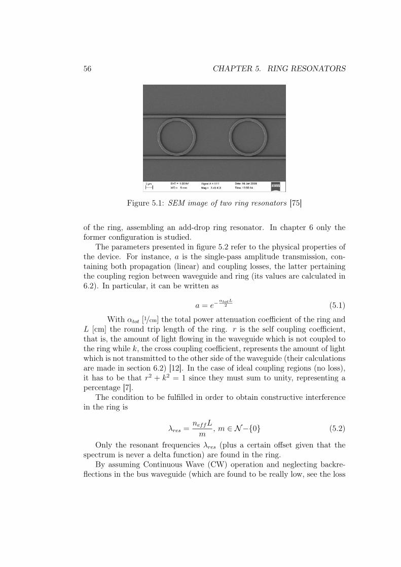
56 CHAPTER 5. RING RESONATORS
Figure 5.1: SEM image of two ring resonators [75]
of the ring, assembling an add-drop ring resonator. In chapter 6 only theformer configuration is studied.
The parameters presented in figure 5.2 refer to the physical properties ofthe device. For instance, a is the single-pass amplitude transmission, con-taining both propagation (linear) and coupling losses, the latter pertainingthe coupling region between waveguide and ring (its values are calculated in6.2). In particular, it can be written as
a = e−αtotL
2 (5.1)
With αtot [1/cm] the total power attenuation coefficient of the ring andL [cm] the round trip length of the ring. r is the self coupling coefficient,that is, the amount of light flowing in the waveguide which is not coupled tothe ring while k, the cross coupling coefficient, represents the amount of lightwhich is not transmitted to the other side of the waveguide (their calculationsare made in section 6.2) [12]. In the case of ideal coupling regions (no loss),it has to be that r2 + k2 = 1 since they must sum to unity, representing apercentage [7].
The condition to be fulfilled in order to obtain constructive interferencein the ring is
λres =neffL
m, m ∈ N−0 (5.2)
Only the resonant frequencies λres (plus a certain offset given that thespectrum is never a delta function) are found in the ring.
By assuming Continuous Wave (CW) operation and neglecting backre-flections in the bus waveguide (which are found to be really low, see the loss

5.1. INTRODUCTION AND PARAMETERS 57
Figure 5.2: Ring resonator and parameters [7]
in section 6.2), the ratio between transmitted and input field in the case ofall-pass rings can be written as [7]:
EpassEinput
= ei(π+φ)a− re−iφ
1− raeiφ(5.3)
Where φ = βL is the single-pass phase shift. To obtain the intensitytransmission, equation (5.3) has to be squared, obtaining
T =IpassIinput
=a2 − 2ra cos(φ) + r2
1− 2ar cos(φ) + (ra)2(5.4)
A peculiar phenomenon appears with reference to critical coupling, inwhich the transmission at resonance drops to 0. Critical coupling is thecondition for which the coupled power is equal to the power loss in the ring,and therefore (1−a2) = k2 leading in the case of ideal couplers to r = a [76].The other conditions are called undercoupling, when the injected power isless than the loss in the ring (r > a), and overcoupling, when the injectedpower overcomes the total amount of loss (r < a).
In figure 5.3 some of the most important spectral parameters for ringresonators are presented.
The Full Width at Half Maximum (FWHM) is a common parameter usedto describe the spectral broadening of the resonance. The lower the FWHMthe more selective and “notch-like” is the filter, being it able to react to asmall amount of frequencies only. In the case of all-pass ring resonators itcan be expressed by [7]
FWHM =(1− ra)λ2
res
πngL√ra
[m] =(1− ra)c
πngL√ra
[Hz] (5.5)
From the equation above it is possible to notice that the parameter in-creases with increasing linear loss and decreases when the ring has a largeradius.

58 CHAPTER 5. RING RESONATORS
Figure 5.3: Output spectrum of an arbitrary ring resonator
Another important indicator of the quality of the ring resonator is theFree Spectral Range (FSR), which is used to express the distance betweentwo consecutive resonant dips. It can be written as [7]
FSR =λ2res
ngL[m] =
c
ngL[Hz] (5.6)
The FSR depends heavily on the length of the ring, with large ones dis-playing closer resonances. In most applications the FSR is required to belarge and therefore small rings are preferable. Small rings are particularlyeasy to fabricate out of silicon because of the high refractive index differenceleading to a tight confinement of the mode inside the waveguide (see section3.2).
Furthermore, the finesse is defined as the ratio of FSR and resonancewidth as
Finesse =FSR
FWHM=
π√ra
1− ra(5.7)
The finesse represents the number of round trips that a light signal isable to complete inside the ring before its initial energy is reduced by 1/e .As a consequence, it is directly dependent on the linear loss and thus on thelength of the silicon loop.
Similar to the finesse is the quality factor (Q). It is defined as

5.2. PHYSICAL PROPERTIES AND FABRICATION PROCESS 59
(a) Finesse (b) Quality factor
Figure 5.4: Finesse and quality factor versus ring length for different linearloss parameters [78]
Q =λres
FWHM=
πngL√ra
λres(1− ra)(5.8)
It represents the number of amplitude oscillations that the light signalperforms inside the ring before its initial energy is reduced by 1/e. It is alsoproportional to the ratio of the stored optical energy inside the ring and theenergy loss rate [77]. In this case there is no direct dependence on the lengthof the ring (covered by L at the numerator) while the reliance on the linearloss remains.
In figure 5.4 finesse and quality factor are plotted against the round triplength of the ring and their response to ring radius and loss is clearly notice-able.
The last parameter is the ER (see section 4.4.2) which relates to thedifference in dB between the maximum and the minimum transmission (atresonance), that is
ER = 10 log10(TmaxTmin
) (5.9)
5.2 Physical properties and fabrication process
5.2.1 Fabrication
One of SOI ring resonators main advantage is the ease of fabrication. Sincethey are built out of silicon, the well-known and efficient technologies used inintegrated electrical circuits can be employed [79]. The devices are usuallycarved on a silicon wafer on which lithographic techniques are applied in

60 CHAPTER 5. RING RESONATORS
Figure 5.5: Lithographic process [80]
order to shape the bulk silicon into a specific pattern depending on the devicethat is being built. The production process can be subdivided in four maincategories: film deposition, patterning, etching and, if need be, doping. Theschematic of a common lithographic process can be seen in figure 5.5.
Among the different methods for growing layers of a certain material,Plasma Enhanced Chemical Vapor Deposition (PECVD) is mainly used todeposit a thin film of a given substance by virtue of chemical reactions causedby plasma reacting gases [81]. While PECVD is commonly utilized in theindustry because of its speed, it does not provide a high degree of accuracy,which is the reason why another technique called Molecular-Beam Epitaxy(MBE) is preferable when high precision is required. MBE takes place in ahigh vacuum environment in which single molecules of a specific material areshot one after the other into a target position in the substrate, obtaining anexceedingly high accuracy, while the downside is the low deposition rate [82].Silica layers can also be obtained by direct oxidation of the silicon after airexposure (passivation) [83].
To model the target layer accordingly to the specific outline of the devicea chemical photoresist layer is applied on the wafer by means of spin coating.On top of the resist a photomask of a given shape is then deposited [84]. Thesample is subsequently shined with Ultraviolet (UV) light (UV lithography)in the case of low-accuracy mass-producted devices or exposed to excitedelectrons (electron beam lithography) to obtain sub-10 nm resolutions [85].The photoresist layer not protected by the photomask changes its chemi-cal composition so that it can be developed, meaning that it reacts with asuitable chemical (called developer), and it is subsequently easily removed(positive resist), while when the resist is negative the removed part is the

5.2. PHYSICAL PROPERTIES AND FABRICATION PROCESS 61
one which was not exposed to the high energy radiation.Etching is the supervised ablation of certain areas of the wafer in order
to dispose of unwanted lumps of material, to free space for a subsequentdeposition or simply to polish a surface so to obtain a pure boundary andconsequently limiting scattering, loss and recombination [85]. The two mainetching techniques are called dry etching (employing plasma) and wet etching(utilizing a liquid chemical reactant). The ablating agent only reacts withareas of the device not covered by the photoresist which therefore allowsthe fabrication of customly designed devices. Afterwards, the remainingphotoresist is removed, usually with a liquid solution called “resist stripper”that causes the resist to detach from the substrate.
Finally, a paramount step in nanofabrication is doping, that can be carriedout before the photoresist removal or afterwards if no specific doping profileis needed. To dope silicon, foreign ions (Group III elements -primarily Boron-in the case of p-doping or Group V elements -primarily Phosphorus- in thecase of n-doping) are utilized. First, the wafer is annealed (exposed to hightemperatures for a suitable amount of time and subsequently cooled down) toallow dopant atoms to attach and penetrate into the bulk. Ion implantationand diffusion doping are the most common doping methods. In the case ofdiffusion, dopant atoms are introduced at the wafer surface and from therethey diffuse in the silicon by sheer concentration imbalance creating a dopinggradient rapidly decreasing while moving away from the surface [86]. Whenit comes to ion implantation, the dopant ions are accelerated and made toimpinge on the wafer surface. The penetration depth depends on the energyof the single ion and since it is a statistical process a certain doping gradientis still recovered, even though it is concentrated in the bulk and not on thesurface [87]. However, particular care must be taken since high energy ionscan deal damage to the device.
5.2.2 Physical properties
SOI ring resonators entail high contrast waveguides, since at the usual com-munication wavelengths (around 1550 nm) nSi ' 3.477 while nSiO2 ' 1.444[88]. The high contrast results in tight confinement of the optical mode andas a consequence allows compact bends without overly compromising theloss. As already pointed out in figure 3.8, TE modes are mainly overlappingwith the cladding via the lateral sidewalls of the waveguide. These verticalsidewalls are rough surfaces because usual polishing methods (such as etch-ing, see section 5.2.1) are not effective when the surface is not horizontalwith respect to the plane of the wafer. As a consequence, it is paramount tolessen their interaction with the optical mode, for instance by reducing the

62 CHAPTER 5. RING RESONATORS
height of the waveguide, which in turns means having to increase the widthto allow the first mode to propagate (see section 3.3). Another possibilityis to use TM polarized light that extends mostly over the smooth horizontalsurfaces of the waveguide (see figure 3.8). However, TM modes are looselybound to the waveguide and since they interplay more extensively with thecladding they cannot be used in the case of tight bends due to the fact thatthe radiation loss would be detrimental [7].
Another consequence of the high contrast is a massive dispersion, suchthat the group index is almost twice as large as the effective index (for com-parison, see figure 6.44 (b) and figure 6.45 (a)) [7]. Furthermore, they arealso extremely sensitive to dimensional variations.
For all these reasons, common waveguide cross sections for ring resonatorsspan from 400 to 500 nm in width and between 200 and 250 nm in height [8],[13], [89], [90]. This particular size allows monomodal propagation, limitingthe detrimental effects caused by a multimode configuration (see sections 3.3and 3.4).
The calculation of the linear loss is somewhat arduous since it dependsheavily on wavelength, waveguide structure and fabrication process, suchthat values ranging from 2 to 20 dB/cm have been recovered [13], [51], [91],[92].
5.3 ApplicationsRing resonators can be used in a large variety of different applications andhave therefore been extensively studied in academic and scientific enviro-ments because of their versatility. Follows a list of the main fields in whichring resonators have proven to be extremely important.
5.3.1 Sensing
For starting, due to their high sensitivity to the variation of the physicalparameters, they are successfully employed for sensing purposes. In partic-ular, the resonance peak shifts abruptly with the coupling, the loss and theeffective refractive index of the resonant structure. By changing any of thoseproperties the frequency spectrum of the ring is greatly affected and the re-sulting variation can be studied to understand its cause. For instance, theycan be used as a strain sensor in order to directly relate to physical deforma-tions. In [93] the authors claimed a sensitivity of ' 0.6 pm/µε meaning thata shift of the resonant wavelength of 0.6 pm can be achieved by applying 1µε. Moreover, rings are also influenced by thermal oscillations so that it is

5.3. APPLICATIONS 63
Figure 5.6: Biosensing [96]
possible to achieve sensitivities up to 230 pm/C, which means that a shift of230 pm in the resonant wavelength is achievable with just 1 C variation [94].Important applications are also found in biology when it comes to label-freebiosensors set up to detect the presence of a specific analyte. They consistof a ring resonator with a surface which is chemically modified by addingreceptor molecules that are selective to the analyte to be detected. The ringis later flooded with a liquid solution and the spectral response retrieved.The spectrum of the ring is different whether in the solution the analyte ispresent or not (figure 5.6) and its impact on the resonance peaks depends onits concentration, allowing more accurate and less expensive measurementscompared to other techniques that need labeling of the analyte [95]. Thesensitivity of the device can be measured by considering how much the ad-hering analyte increases the thickness of the waveguide. For instance, in [78]a waveguide of size 480×220 nm is considered and the authors claim thatfor practical values of the thickness the response is linear. In particular, it isfound as 0.158 nm/nm in the case of TE mode and 0.290 nm/nm in the case ofTM mode, which can be explained with the reduced waveguide confinementof the latter.
5.3.2 Optical buffer
Additionally, ring resonators are traditionally utilized as optical buffers.CROW systems of different rings coupled together (high order ring res-onators) are effective to obtain optical delay lines in photonic integratedcircuits, since near resonance the optical intensity inside the ring is extremely

64 CHAPTER 5. RING RESONATORS
Figure 5.7: Ring resonator DEMUX [77]
high. The time delay-bandwidth product is given by [7]
TCROW =N
2π(5.10)
Where N is the order of the filter (that is, the number of cascaded rings).The delay thus obtained can be as large as 200 ps for filters of order 40, asclaimed in [97].
5.3.3 MUX/DEMUX
Another important application of ring resonators is the multiplexing/demul-tiplexing of the signal in the case of WDM or DWDM coding. These modu-lation techniques consist on strikingly enhancing the data rate of an opticalchannel by sending simultaneously light at different frequencies provided thatthe spectrum of the signal is clearly resolvable. In particular, when it comesto WDM the light pulses (called channels) are separated by 100 GHz (namely,' 0.4 nm at λ = 1550 nm) while for DWDM it is 50 GHz (that is, ' 0.8nm at λ = 1550 nm) [33]. As can be seen in figure 5.7, by employing ringswith different resonant peaks as a DEMUX system it is possible to redirect aparticular channel to its specific detector and, as a consequence, successfullydemodulate the input signal [98]. However, the rings are exceedingly proneto fabrication defects and as a result they have to be thoroughly tested beforebeing used for such purpose. Moreover, high order filters provide an improvedspectral behavior since they display a more uniform pass band over a widerwavelength range, besides the improved ER outside the desired bandwidth[7].

5.3. APPLICATIONS 65
Figure 5.8: Carrier depletion modulator [99]
5.3.4 Ring modulator
The last application of ring resonators presented is the modulation, which isthe topic of the thesis and will be further discussed in chapter 6. A siliconring modulator is used as an OOK modulated device in which the operatingwavelength is close to the resonance peak such that high ERs can be obtainedwith just a relatively small shift of the dip due to a variation in the opticalproperties of the waveguide. To do so, high slopes (low FWHM) rings areneeded, resulting in high Q and finesse. On the other hand, if this parameteris too large, the overall switching time of the device will be negatively affectedbeing it dependent on how fast the optical power inside the ring is dissipated[7]. In particular, the 3 dB cut-off frequency can be written as [11]
f3dB =fOPT · fEL√f 2OPT + f 2
EL
(5.11)
Where
fOPT =c
Q(0V ) · λres(0V )(5.12)
Is the optical component stemming from the lifetime of the photons inthe waveguide (Q and λres are considered at zero bias applied) while
fEL =1
2πRC(5.13)
Is the standard bandwidth of the electric circuit due to the RC constantof the device and as such it strongly depends on the physical size of thedevice.
Among the FOMs in the case of ring modulators, VπL is widely consideredas one of the most important parameters to be taken into considereation (seesection 4.4.5) and can be expressed as [99]

66 CHAPTER 5. RING RESONATORS
Figure 5.9: Output spectrum of a depletion mode ring modulator versus bias[101]
VπL =λ · V
2 ·∆neff(5.14)
The modulation occurs by virtue of the refractive index variation (plasmadispersion effect), which is caused by the oscillation of the carriers in thewaveguide due to the swing of the applied voltage (see section 4.3.3). Twoare the main techniques employed: carrier injection and carrier depletion.
In the case of carrier depletion the ring cross section of the horizontaljunction version can be seen in figure 5.8. The main structure is a PNdiode whose doping concentration extends over the waveguide core, whichcan be mixed (top), n-only (middle) or p-only (bottom). Better performingmodulators utilize the so-called vertical junction, in which the p and n areasare put one on top of each other [100].
The device operates in depletion mode, meaning that, when a reversevoltage is applied, the space charge region becomes larger and therefore lesscarriers are found in the waveguide, causing a variation in the refractiveindex. The spectrum thus obtained can be seen in figure 5.9. When thevoltage is negative, the modulation results in a slight red-shift of the resonantfrequency followed by a mild ER decrease.
Positive voltages are usually the case for injection mode modulators,based on PIN diodes in which the intrinsic layer (which is actually slightlydoped) extends over the waveguide. As can be seen in figure 5.9, positivevoltages lead to a blue-shift of the resonant wavelength and a steep decrease

5.3. APPLICATIONS 67
of the ER. The modulation is much more effective since the intrinsic region isflooded with carriers (the diode is turned on, in particular when V is largerthan 0.7 V in figure). The downside is that a current is flowing in the deviceand the bandwidth is much smaller since it depends on the minority carrierslifetime (resulting in bandwidth of around 1 GHz [71]), while in the formercase it depends on the junction capacitance discharge which is much faster(with modulation speed up to 20 GHz [71]) [7]. Consequently, if the goalis to obtain an effective modulation with a small VπL it is better to resortto carrier injection. On the other hand, if the focus is on the speed of thedevice, one better resort to carrier depletion.
A possible improvement of the pin modulator is by means of pre-emphasis,which consists on using two different bias levels to speed up the modulationfrequency. Results of the order of tens of GHz are retrieved in [102].

68 CHAPTER 5. RING RESONATORS

Chapter 6
Simulation Results andDiscussions
This chapter presents the main results obtained in this thesis work. The pro-grams used are primarily MATLAB and Lumerical. In particular, Lumericalprovided the simulation for what regards the physical parameters of the ringmodulator, such as coupling coefficient, flowing current and effective refrac-tive index, while MATLAB made the analysis of the data possible in orderto retrieve the output spectrum of the device and the calculation of the mostimportant parameters, such as FSR, finesse andVπL. MATLAB was alsoemployed to code and implement the effective refractive index method. Asregards the data, it was collected for different configurations of the device.Among the different parameters considered, the lateral slab height, the in-trinsic region width, the lateral slab width, the doping concentration and thering bend.
6.1 Effective index methodThe effective index method, as presented in [103] and [104], is a numericalprocess useful to calculate the effective refractive index of a given waveguide.It is based on the subsequent approximations of different areas of the waveg-uide by calculating their partial refractive indices and consequently mergingthe sub-waveguides thus obtained in order to retrieve the final refractive in-dex. First, the columns (n1 − n4 − n7 → neff,1, n2 − n5 − n8 → neff,2 andn3 − n6 − n9 → neff,3) are considered and afterwards the remaining rows(neff,1− neff,2− neff,3 → neff ) are elaborated (consider a subdivision of thewaveguide as in figure 6.1, where the optical waveguide of size w× t is in thecentral area n5) .
69

70 CHAPTER 6. SIMULATION RESULTS AND DISCUSSIONS
Figure 6.1: Waveguide subdivided in small regions [103]
This method has been implemented in MATLAB in the case of a ribwaveguide whose cladding is made of air (n = 1) or SiO2 (n = 1.44) at1550 nm wavelength. The waveguide is made of silicon with n = 3.45. Therefractive index is extracted sweeping over different lateral heights, rangingfrom 50 to 110 nm while the waveguide itself is 220 nm high and 460 nmwide. In figure 6.2 the transcendental equation to be solved is shown withreference to an air cladding for the central column (made up of SiO2, Si andair).
-1 -0.5 0 0.5 1
Kappa [nm-1
] 107
-20
-15
-10
-5
0
5
10
15
20
Figure 6.2: Transcendental equation solved in the case of air as cladding
As can be seen in figure 6.3, with increasing slab height the effectiverefractive index grows as well, being the refractive index of the waveguidelarger than the one in the surroundings. At the same time, it is clearlynoticeable that, having an air cladding (whose refractive index is the lowest),the overall refractive index of the waveguide is significantly lower for all theconfiguration tested, with values spanning from −1.7% for the lowest slabheight considered to −1.05% in the case of the 110 nm slab height.

6.2. COUPLING COEFFICIENT 71
The results are realistic and can be compared, for instance, with thoseretrieved in Lumerical and shown in figure 6.40. Another comparison can bedrawn with [105], where, however, the authors considered a strip waveguideand therefore the values are lower, namely spanning from 2.36 at λ = 1550nm.
Figure 6.3: Results plotted as a function of the slab height in the case of airand silicon dioxide cladding
6.2 Coupling coefficientTo calculate the coupling coefficient between the straight waveguide acting asthe input/output channel for the system and the ring, the Lumerical FDTDsimulator has been used. The model employed is shown in figure 6.4 inrelation to strip waveguides. In particular, the waveguides considered areboth 460× 220 nm. In the case of the rib configuration, the lateral slab hasa height of 70 nm.
As regards the mode solver, a fine mesh has been set up in the areabetween the two waveguides in order to achieve a greater accuracy in thecalculation, and the signal launched in the input waveguide has a bandwidthranging from 1500 to 1600 nm, as can be seen in figure 6.5, consequentlycovering the main transmission window (C-band). The actual simulationarea does not entail the entire ring/waveguide structure but only a section,so that the calculation proceeds faster without affecting the final results.
In figure 6.6 the behavior of the rib waveguide is analyzed taking intoconsideration a certain wavelength only, namely 1556 nm. It can be seenthat the self-coupling coefficient R = |r|2 decreases both with the reductionof the coupling distance (as explained theoretically in section 3.5 due to astronger overlap between the evanescent fields) and with more sizeable rings,

72 CHAPTER 6. SIMULATION RESULTS AND DISCUSSIONS
(a) Side view of the model (b) Top view of the model
Figure 6.4: Model built with Lumerical. The oxide cladding has been disabledfor examination purposes
Figure 6.5: Signal launched, details
because the effective coupling length is larger when the ring waveguide takeslonger to bend away. On the other hand, as expected, the cross-couplingcoefficient K = |k|2 behaves in the opposite way.
In figure 6.7 the light intensity is plotted along the structure. The topbranch is the straight waveguide while the bent bottom one is the inputchannel of the ring resonator. It is clearly noticeable that when it comes tolong radii and small gaps the amount of light coupled is remarkably larger(namely, around 50%) than in the other case, that is, with a small ring andlarge gap between the waveguides (namely, around 1%).
When a comparison with the wavelength is made, it is found that shorterwavelengths result in a lesser coupling, as expected from the theory (section3.4.2). The result of such a comparison can be found in figure 6.8.

6.2. COUPLING COEFFICIENT 73
(a) Self-coupling coefficient (b) Cross-coupling coefficient
Figure 6.6: Coupling coefficients in the case of a rib waveguide versus thegap distance between the two waveguides for different bends
(a) 10 µm radius ring and 100 nm gap (b) 5 µm radius ring and 300 nm gap
Figure 6.7: Light propagation in the structure for different configurations
It is interesting to find the amount of loss in the coupling region. In alossless coupler we would have R+K = 1, but in this case the result is quitedifferent and can be seen in figure 6.9. The loss is found to increase whenthe cross-coupling coefficient is larger, meaning in the case of small gaps andlong wavelengths. Overall though, it is really low, spanning from 0.9% forsmall gaps and radii to less than 0.1% when the coupling distance is large.
Afterwards, the analysis of the difference between rib and strip waveguidesis carried out. As depicted in figure 6.10, the rib waveguide is significantlymore efficient at coupling compared to the other one, the reason being thedirect dielectric connection between the two waveguides and the consequentspread of the light towards the adjacent channel. The behavior is enhancedespecially when the gap gets smaller.
Finally, with reference to strip waveguides, a comparison between thecoupling coefficient and the wavelength is charted in figure 6.11. The im-provement in coupling capability is strongly determined by the gap width, asfor the rib waveguide; however, it is much more wavelength dependent than

74 CHAPTER 6. SIMULATION RESULTS AND DISCUSSIONS
(a) Self-coupling (b) Cross-coupling
Figure 6.8: Coupling coefficients in the case of a rib waveguide versus thewavelength considered in the case of a ring with radius 7.5 µm
(a) Loss vs gap (b) Loss vs wavelength
Figure 6.9: Loss due to the coupling region in the case of a ring with radius7.5 µm
in the other case, as the curve has a remarkably steeper slope as a functionof the wavelength.
Similar results can be found in [7]. Here the coupling is between twowaveguides which are not bent; however, the same pattern can be extracted,with a minor coupling in relation to short wavelengths and gaps. In addi-tion, by comparing the cross-coupling coefficient per length with the valuesextracted in this thesis work, a certain affinity can be observed (for instance,as regards the 195 nm gap it is around 0.11 1/µm and when considering thatthe ring is large in size the results are comparable).
6.3 Mode overlapWhen a waveguide is bent, the mode profile experiences a certain degree ofmismatch due to the curvature of the waveguide, resulting in higher losses
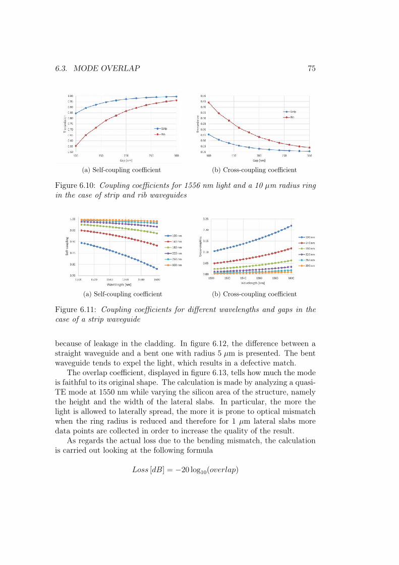
6.3. MODE OVERLAP 75
(a) Self-coupling coefficient (b) Cross-coupling coefficient
Figure 6.10: Coupling coefficients for 1556 nm light and a 10 µm radius ringin the case of strip and rib waveguides
(a) Self-coupling coefficient (b) Cross-coupling coefficient
Figure 6.11: Coupling coefficients for different wavelengths and gaps in thecase of a strip waveguide
because of leakage in the cladding. In figure 6.12, the difference between astraight waveguide and a bent one with radius 5 µm is presented. The bentwaveguide tends to expel the light, which results in a defective match.
The overlap coefficient, displayed in figure 6.13, tells how much the modeis faithful to its original shape. The calculation is made by analyzing a quasi-TE mode at 1550 nm while varying the silicon area of the structure, namelythe height and the width of the lateral slabs. In particular, the more thelight is allowed to laterally spread, the more it is prone to optical mismatchwhen the ring radius is reduced and therefore for 1 µm lateral slabs moredata points are collected in order to increase the quality of the result.
As regards the actual loss due to the bending mismatch, the calculationis carried out looking at the following formula
Loss [dB] = −20 log10(overlap)

76 CHAPTER 6. SIMULATION RESULTS AND DISCUSSIONS
(a) Straight waveguide (b) Bent waveguide with radius 5 µm
Figure 6.12: Field pattern difference in the case of a straight and of a bendwaveguide for a 1 µm wide and 110 nm high slab
(a) 700 nm slab width (b) 1 µm slab width
Figure 6.13: Mode overlap versus ring radius for different heights of thelateral slab
And the results are plotted in figure 6.14.As we can see, the losses are quite low and almost constant for radii down
to 5 µm, size at which they snowball reaching, for certain configurations, 3dB, which is half the transmitted power. Consequently, we can conclude thatrings with radii as small as 5 µm are still viable in terms of loss, with greatincrease of the FSR and other important parameters. In particular, the lossat common radius lengths (7-10 µm) are close to the ones considered in [7](around 0.04 dB), proving the accuracy of the calculation.

6.4. MODULATOR 77
(a) 700 nm slab width (b) 1 µm slab width
Figure 6.14: Loss versus ring radius for different heights of the lateral slab
6.4 ModulatorIn this section, the modulating component of a silicon ring resonator is stud-ied with respect to different physical parameters. The modulator chosen isthe carrier-injection-based pin diode and as such the applied voltage is posi-tive. The structure, that can be seen in figure 6.15, is a cross section of thering (the raised structure in the center of figure 6.15 (a)) and it comprisestwo electrodes (anode and cathode, in dark grey in figure 6.15 (a)) arrangedon top of two highly doped silicon pedestals. The silicon regions are conter-minous with two smaller elongated silicon slabs connecting together at thecenter (where the waveguide is placed) and the background material is SiO2.As regards the physical dimensions, the optical waveguide has height L of450 nm and width T of 220 nm. The lateral slab height h is initially set to110 nm while the width w is 1.7 µm. Lastly, the device is studied as it wasstraight (no bend applied in MODE solver).
The procedure employed to simulate and analyze the behavior of themodulator is the following. First, with Lumerical DEVICE, the carrier dis-tribution and consequently the variation in the refractive index (see section4.3.3) are calculated for a fine grid of points around the central waveguide bysweeping over a range of voltages to simulate the current flowing in the pindiode. Other parameters that are saved in this step are the charge density(both in the structure in its entirety and the value in the waveguide) andthe current density. Afterwards, the refractive index distribution is loadedon Lumerical MODE where calculations related to light propagation in thedevice are carried out. The values of the refractive index for different levels ofthe applied voltage are retrieved in this step. From the refractive index onecan directly derive the difference in the refractive index and the loss causedby the carriers in the channel.

78 CHAPTER 6. SIMULATION RESULTS AND DISCUSSIONS
(a) DEVICE version
(b) MODE version
Figure 6.15: Device under studying. The cladding has been removed for clar-ity purposes
6.4.1 Intrinsic region width
The first parameter to have been studied is the width of the intrinsic region.In this particular case, the doping is set to be homogeneous in different areas,as explained in table 6.1.
The background doping is set to a lower value compared to other simula-tion setups found on the Lumerical website (with value of 1015) because thatlevel of doping was seemingly too high for being an intrinsic region (whichis usually only lightly doped). However, a further analysis has been carriedout sweeping over different background dopings in section 6.4.5 for a differ-ent model structure. The contact regions are heavily doped since they aretouching the metal electrodes and a low series resistance has to be achieved.
The constant doping model is not realistic but it is a good starting pointto evaluate the performance of the device in order to choose the best config-uration possible. Starting from section 6.4.4, however, the constant dopinghas been substitute with a more realistic diffusion doping profile. A glimpse

6.4. MODULATOR 79
Table 6.1: Doping concentration
Region Concentration Type
Contact region 1020 n/p
Slab region 1018 n/p
Background 1013 n
of the doping distribution around the waveguide is provided in figure 6.16 fordifferent voltage levels.
(a) 0 V applied (b) 2 V applied
Figure 6.16: Doping profile in dB at the center of the device. n doping ontop, p doping at the bottom
Another unrealistic parameter is the voltage, here spanning from 0 to 3V, which is an overly high value with respect to the physical size of the ringand the objective of the modulation. Starting from section 6.4.4, however,the sweep has been reduced spanning from 0 to 2 V, which is more practical.
First of all, the results obtained by using DEVICE are analyzed in figure6.17. The charge density (since the monitor used is 2D) is retrieved consid-ering both the entire structure (a) and focusing on the waveguide area (b).The behavior resembles that of a diode since we have a steep increase in thecarriers when the voltage exceeds 0.75 V, which is arguably the thresholdvoltage of the diode.
Afterwards, by using MODE, the refractive index is retrieved and in figure6.18 its modulation is presented for both real (n) and imaginary (representedby the linear loss factor α) part. As we can see in (a), the refractive index dif-ference increases when the intrinsic region width is reduced, because there ismore current flowing in the device leading to a greater carrier concentration.

80 CHAPTER 6. SIMULATION RESULTS AND DISCUSSIONS
(a) Charge density in the entire device (b) Charge density around the waveguide
Figure 6.17: Charge density in the device versus the applied bias
However, the modulation in the case of 1 V applied is small compared to theothers because the diode is still not fully turned on, as it is more evidentin (b) where the diode influence on the data is clear, since the values arereally low up to 0.75 V and increase rapidly afterwards. In particular, thefocus on the low voltage regime is highlighted in the inset. Here it is possibleto notice that the loss due to the carriers when there is no to little voltageapplied depends heavily on the width of the intrinsic region. For modulationpurposes, the loss at 0 V should be as low as possible, and therefore in lightof the data collected all the subsequent measurement will employ a structurefor which the intrinsic region width is 0.6 µm.
(a) Variation in n versus intrinsic regionwidth for different voltages
(b) Linear loss versus applied voltage for dif-ferent intrinsic region widths
Figure 6.18: Refractive index change and loss with focus on the intrinsicregion width and its variation

6.4. MODULATOR 81
6.4.2 Lateral slab height
The next step, once the intrinsic region width has been set to 600 nm, is todetermine the best height of the lateral slabs. All the remaining modelingparameters are taken equal to the previous step, except for the backgrounddoping which is now n type. In figure 6.19 the current density is plottedagainst the voltage applied and the different slab heights. As expected, thebehavior is still diode-like with threshold somewhere around 1 V. It is im-mediately noticeable that higher lateral slabs result in an increased currentand charge density (since the current monitor is in 2D) present in the device.It is also important to point out that the dependence of the charge densityon the sweeping parameter is more pronounced in this case than in the pre-vious analysis, due to the larger length of the lateral slabs compared to theincreased number of carriers due to a narrowing of the intrinsic region.
(a) Current versus voltage (b) Charge density (in the entire device) versusvoltage
Figure 6.19: DEVICE results for different slab heights
As regards MODE, figure 6.20 depicts the behavior of the refractive in-dex with different heights and voltages applied. Again, the real part of therefractive index is better modulated when high currents flow and thereforewith high lateral slabs. At the same time, however, we can see that whenthe slabs allow the light to spread more, the overlap with the carriers islarger and therefore the loss at low bias (below threshold) increase (b). Thisagain is the major discriminating factor ruling out overly high lateral slabs,responsible also for an increase in the current and the charge in the deviceand consequently worsening the speed and the energy consumption of thedevice. Because of this, a reasonable slab height of 70 nm is chosen for thenext steps.

82 CHAPTER 6. SIMULATION RESULTS AND DISCUSSIONS
(a) Difference in n due to different heightsand voltage
(b) Linear loss versus applied voltage for dif-ferent slab heights
Figure 6.20: MODE results for different slab heights
6.4.3 Slab width
In this case the current flowing in the device is higher than in the previous twosections and as a consequence additional voltage steps have been employedin order to let the CHARGE simulator in DEVICE converge, for a total of25 data points (instead of the previous 13). The width range spanned in thissimulation goes from 0.7 to 1.7 µm.
As regards DEVICE, the charge density is plotted in figure 6.21. Theresults are consistent with the previous calculations.
(a) Charge density of the entire device (b) Charge density around the waveguide
Figure 6.21: Charge density versus voltage for different widths
With MODE the refractive index variation and loss are evaluated as canbe seen in figure 6.22. First of all, in (a) it can be seen that by reducingthe distance between waveguide and electrodes the modulation capabilitystrongly increases. At the same time, in (b), the linear loss follows the sameprinciple, but for widths of less than 1 µm it becomes prohibitive at smallbias (at 0.7 µm we have almost four time the loss experienced at 1 µm). For

6.4. MODULATOR 83
this reason the next steps evaluate the behavior of the device for larger slabwidths.
(a) Variation of n versus slab width for differ-ent voltages
(b) Linear loss versus voltage for different slabwidths
Figure 6.22: MODE analysis of the device
6.4.4 Doping concentration
A further improvement can be represented by a more realistic doping profile.DEVICE allows to set up a diffusion kind of doping starting from a sur-face (see section 5.2.1). In this section, the background doping is still set asconstant and its type and concentration are the same as the previous steps.However, doping diffusion has been simulated starting from the contact re-gion and the lateral slab. In particular, the diffusion profile has been set toGaussian and the doping intensity spans from 1019 to 1.5 · 1020 cm−3 in thecase of the contact doping and from 1017 to 1.5 · 1018 cm−3 in the case ofthe slabs (from now on, 0.1 to 1.5 using as reference concentration (that is,1) the case 1018 − 1020 cm−3). Three different slab widths have been ana-lyzed, namely 1 µm, 1.35 µm and 1.7 µm (shorter versions have previouslybeen discarded in section 6.4.3). In figure 6.23 the doping profile of the areaaround the waveguide is charted with reference to the longest slab and fordifferent voltage levels.
To show the general behavior of such a device, in figure 6.24 and 6.25the electrical and optical main properties for the 1.35 µm case are shown(the behavior of the other two configurations is alike). In particular, it isimmediately noticeable that an increase in the doping corresponds to a moreeffective modulation (figure 6.25 (a)) and consequently a more pronouncedlinear loss (figure 6.25 (b)). At the same time, as expected, both the currentand the charge density in the waveguide increase (figure 6.24 (a) and (b) re-spectively), although for the former a quite noticeable saturation can be seen

84 CHAPTER 6. SIMULATION RESULTS AND DISCUSSIONS
(a) 0 V applied (b) 2 V applied
Figure 6.23: Diffused doping profile in the center of the device. n doping ontop, p doping at the bottom
for high values of the doping concentration (when more than 1.1). Interest-ingly enough, it seems that the slope of the curve representing the variationof the refractive index decreases with a bias larger than 1.5 V, indicating apossible saturation of the device at high voltages.
(a) Current density versus voltage for differentdoping levels
(b) Charge density in the intrinsic region versusvoltage for different doping levels
Figure 6.24: DEVICE data in the case of a 1.35 µm wide lateral slab (valuesin the legend to be multiplied by 1018 or 1020 accordingly to the region)
At the same time, when depicting the optical properties versus the dopingconcentration, one can deduce that the modulation capability flattens withhigh level of doping as well (figure 6.26). In particular, in (a) the plottedmodulation capability shows a steep increase when the doping level is low,but it quickly stabilizes (especially when less voltage is applied). In (b), thelinear loss shows a similar behavior.

6.4. MODULATOR 85
(a) Variation in n versus voltage for differentdoping levels
(b) Linear loss versus voltage for different dop-ing levels
Figure 6.25: MODE data in the case of a 1.35 µm wide lateral slab (valuesin the legend to be multiplied by 1018 or 1020 accordingly to the region)
(a) Variation in n at different bias (b) Linear loss at different bias
Figure 6.26: Optical properties displayed versus doping concentration
From the results above, as a rough approximation it is possible to claimthat a bias higher than 1.5 V does not result in a significant modulationadvantage and it is therefore to be ruled out. Nevertheless, below 1.5 V thediode is not fully on and a much larger improvement can be achieved byincreasing the voltage. Analogously, in the case of the doping concentration,when it is below a certain threshold a large gain is recovered by increasing thediffusion intensity while if it is excessive it will be close to useless modulation-wise but detrimental when it comes to the loss at zero bias (see the inset infigure 6.25 (b)) and the total amount of charge in the device (figure 6.24 (b)).Moreover, at the same time the current behavior becomes erratic (figure 6.24(a)), therefore meaning that high doping profiles have to be avoided.
It is also important to point out that the results obtained so far arecompatible with the ones previously retrieved with a costant doping profile,but they are slightly worse due to the more realistic doping profile which

86 CHAPTER 6. SIMULATION RESULTS AND DISCUSSIONS
results in an overall less efficient modulation. Moreover, they are alignedto the Soref-Bennett equations (4.8) and (4.9) when substituting the carrierconcentration of the formulae with an arbitrary reference value stemmingfrom the concentration bar of figure 6.23.
The next step comprises the comparison between the three different widths.In figure 6.27 the linear loss at 0 and 1.5 V is considered. In particular, in(a) the loss is strikingly lower in the case of longer slabs. Interestingly, thereis virtually no difference between the 1.35 µm and the 1.7 µm configurations.For useful doping concentrations in (b) the behavior is still the predictedone, with increasing loss while decreasing the waveguide/contact distance;however, once again the largest difference is found between 1.0 and 1.35 µm.
(a) Linear loss at 0 V (b) Linear loss at 1.5 V
Figure 6.27: Linear loss versus doping concentration for different widths con-sidered
In figure 6.28 the real part of the refractive index is analyzed at twodifferent bias levels. Considering (a), it is possible to point out that there isalmost no difference between the two longest devices. Furthermore, at verylow doping concentration the 1.7 µm version has the upper hand compared toboth the others and retains the advantage over the 1.35 µm long slabs up todoping levels of 0.9. When the diode is fully turned on at 1.5 V (b), however,the medium-sized device catches up earlier at concentrations around 0.4. Theshort slabs have definitely the advantage, even though at the expense of ahigher overall loss.
Consequently, the current output of the device is studied in figure 6.29.The curves are similar for both devices, even though the scale in the y-axis isof course different. As already pointed out by looking at figure 6.24, at highdoping concentrations the current behavior is somewhat erratic since it showsan interesting decrease which is less pronounced at high bias or short size ofthe device. In particular, the 1.0 and 1.35 µm versions display a quite similarbehavior and are preferable in this regard considering that higher currents

6.4. MODULATOR 87
(a) 1 V applied (b) 1.5 V applied
Figure 6.28: Variation in n versus doping concentration for different widths
result in less series resistance and thus increasing the modulation speed ofthe device, although the downside is a more detrimental power consumption.
(a) 1 V applied (b) 1.5 V applied
Figure 6.29: Current versus doping concentration for different widths
As regards the charge, figures 6.30 and 6.31 show the charge densityaround the intrinsic region and the structure in its entirety respectively.Clearly, a larger device has the drawback of a sizeable amount of charge,resulting in a more deleterious RC constant. As expected, denser doping con-centrations increase the amount of charge. It is interesting to point out thatboth the 1.35 and 1.7 µm configurations are fairly similar and the amount ofcharge is quite comparable.
Afterwards, the resistivity and capacitance of the junction are calculatedfor the 1.35 µm wide slab version and the result is reported in figure 6.32.When comparing with [89], the capacitance is seen to be similar, while theresistance (calculated by considering a ring of radius 7.5 µm) is 3 to 4 orders ofmagnitude different. However, when compared to [8] or the results obtainedin [106], the resistivity is found to be ' 0.1 V·cm which corresponds to thevalues depicted in (b). It is not clear why such a discrepancy in the data

88 CHAPTER 6. SIMULATION RESULTS AND DISCUSSIONS
(a) 1 V applied (b) 1.5 V applied
Figure 6.30: Charge around the intrinsic region versus doping concentrationfor different widths
(a) 1 V applied (b) 1.5 V applied
Figure 6.31: Charge in the entire device versus doping concentration for dif-ferent widths
is retrieved, however the electrical bandwidth calculated with formula (5.13)appears to be overly low when considering the RC constant recovered withthe data shown in figure 6.32.
Subsequently, some important parameters, such as quality factor, finesse,FWHM, FSR, VπL and ER are addressed and discussed. The data has beencollected by means of MATLAB scripts. To retrieve the data, the formulaspresented in sections 4.4 and 5.1 have been employed by considering a 7.5µm long radius (a more thorough analysis of the influence of the bending onthe device is carried out in section 6.4.6). Some parameters have been chosenregarding the physical structure of the device. For instance, the usual linearloss of the silicon waveguide has been set to 4.343 dB/cm, which is an educatedguess (see section 5.2.2). At the same time, the active region in which themodulation takes place has been limited to 65% of the total ring perime-

6.4. MODULATOR 89
(a) Capacitance per meter (b) Resistivity
Figure 6.32: Electrical parameters in the case of 1.35 µm wide lateral slabs
ter, to allow an easy and noise-impervious coupling with the input/outputwaveguide (see figure 6.47). The initial value of the self-coupling has beenchosen so that to be in the critical coupling condition (and therefore equalto the single-pass amplitude transmission of the ring).
In figure 6.33 the behavior of quality factor and finesse is plotted fordifferent doping concentrations. It can be seen that these two parametersare larger with high doping and tend to decrease rapidly as the diode turnson. A comparison can be made with [107], in which a ring of radius 6 µmis considered. The quality factor is reported there as 39.350 which is lowerthan the one in (a) when no bias is applied but, pointing out that the ringis smaller and considering the behavior of the quality factor with respect tothe cavity length (see section 5.1), it is possible to infer that the result isachievable.
(a) Q factor for different doping levels (b) Finesse for different doping levels
Figure 6.33: Q factor and finesse versus voltage in the case of 1.0 µm wideslabs
Moreover, in figure 6.34 the FSR and the FWHM are shown with respect

90 CHAPTER 6. SIMULATION RESULTS AND DISCUSSIONS
to the doping concentration and compared at different lateral slab widths.Both parameters worsen with increasing doping, the FSR being smaller (dueto a slight increase in the group index) and the FWHM being larger (broaderresonances). It is also important to point out that the smallest device de-grades at a larger rate compared to the other two configurations that arerather interchangeable. In the case of the FWHM, in [107] it is reported avalue of 0.04 nm, which is comparable with that in (b) even if the ring insaid paper has a radius of 6 µm.
(a) FSR for different slab widths (b) FWHM for different slab widths
Figure 6.34: FSR and FWHM versus doping concentration
As regards the FOM VπL, calculated using formula (5.14), the resultsobtained at two different voltage levels, namely 1 V and 1.5 V, are shownin figure 6.35. The values are significantly better for the 1.5 V case, sincethe diode is fully turned on and the modulation more effective. As a generaltrend, higher doping concentrations result in better performances, with the1.0 µm wide device obtaining the best results. The results are certainlyrealistically achievable, since for instance in [8] values even lower (namely0.0025 V·cm) are reported. In [102], the modulation efficiency is revealed tobe 0.011 V·cm, which is quite similar to what has been charted in figure 6.35.
The ER, calculated as the difference in dB between the peak of the res-onance and the maximum value of the transmission, is depicted in figure6.36 for two different voltage levels, namely 0.75 V and 1 V. Larger voltagesare not considered since the parameter flattens quickly to small values. In-terestingly, two opposite behaviors are recovered. In the case of the smallbias, the ER is found to increase with the doping concentration. When thediode is properly turned on, however, it is seen to decrease. Furthermore,in figure 6.36 (a) there is a remarkable difference between the short and thelong devices, the former performing better. In (b), on the other hand, theyseem to behave quite similarly. A striking contrast is recovered for such a

6.4. MODULATOR 91
(a) 1 V applied (b) 1.5 V applied
Figure 6.35: V πL versus doping concentration for different slab widths
small bias difference, meaning that the parameter is extremely sensitive tothe concentration of free carriers in the waveguide.
(a) 0.75 V applied (b) 1 V applied
Figure 6.36: ER versus doping concentration for different slab widths
In light of the previous analysis, the optimal configuration found is the1.35 µm wide. Not only is the loss at zero bias low (figure 6.27 (a)) and thecurrent comparable to the shorter configuration (figure 6.29), but also thetotal amount of charge is close to that of the 1.7 µm device (so that therewould be no advantage in choosing the latter) and important parameterssuch as FSR and FWHM do not degrade as fast as in the shortest device.Moreover, the footprint is significantly less pronounced than in the lattercase. When it comes to the applied voltage, it will be set to less than 0.9 Vfor the “on” state. It is true that the diode is not fully on and further biaswill result in a large improvement of the refractive index action. However,based on the parameters calculated in figures from 6.33 to 6.36, the bias hasto be set lower since an effective modulation is already performed at lowervoltages (see figure 6.48) and these parameters generally worsen with more

92 CHAPTER 6. SIMULATION RESULTS AND DISCUSSIONS
bias applied. Furthermore, it is possible to lower the power consumption andthe wear of the device. As regards the doping concentration, the 1.0 setupis arguably the best one because it does not suffer from excessive loss when“off” and at the same time it does not enter the regime in which the currentsaturates (figure 6.29 (b)).
6.4.5 Background doping level
Subsequently, the problem about the constant background doping level (pepi)concentration is addressed. In this regard, both n and p doping types areconsidered. Their concentration spans from 1013 to 1.5 ·1014 cm−3 (from nowon, 1 to 15 using as reference concentration (that is, 1) the case 1013 cm−3).It is important to point out that the background doping has effect only onthe core intrinsic region because the heavily doped lateral regions are notaffected by such a small variation of the carrier density.
In figure 6.37 the electrical properties are charted. In particular, the cur-rent and the charge density are plotted for both n and p background doping.However, no noticeable difference has been found, the two doping types beingvirtually equivalent. By increasing the doping, though, an important factorbecomes noticeable: the current tends to slightly decrease.
(a) Current density for both n and p doping (b) Charge density for both n and p doping
Figure 6.37: Electrical properties at 1.5 V for different doping levels
An interesting finding, which can be seen in figure 6.38, is that the lossat zero bias is lower in the case of p doping, the result being explained bythe reduction of n carriers in the channel (which are the most effective inincreasing the absorption coefficient, see figure 4.5 (b)), as depicted in (b).The data suffers from some oscillations due to inaccuracies of the solver, butthe overall trend is readily extrapolated. It is important to notice, however,that at low background doping levels the two values converge.

6.4. MODULATOR 93
(a) Linear loss for both n and p backgrounddoping
(b) p free carrier in the intrinsic region for bothn and p background doping
Figure 6.38: Loss and carrier concentration for different doping levels
The last observation can be made regarding the modulation capabilityand the variation of the real part of the refractive index. As shown in figure6.39, in the case of low voltages there is no noticeable difference betweenthe two types of doping. With increasing voltage, however, there is a slightadvantage when using n doping. This advantage becomes more clearly de-tectable as the background doping concentration increases.
(a) 1 V applied (b) 1.5 V applied
Figure 6.39: Variation in n due to the background doping
To draw a conclusion, both n and p doping have their own pros and cons.Therefore, the original background doping (as in table 6.1) is maintained forthe future chapters.
6.4.6 Bend
In this section the calculation made with MODE is repeated considering abent structure (to simulate a section of the ring). The bending radius spans

94 CHAPTER 6. SIMULATION RESULTS AND DISCUSSIONS
from 5 to 10 µm (in order to avoid overly penalizing bend losses, see section6.3). First of all, in figure 6.40, a quick comparison between bent and straightwaveguides is made. First, it is possible to notice in (a) that by increasing thebend the refractive index is lower, while its modulation is almost constant.On the other hand, in (b), the linear loss is found to be virtually the samewhen the diode is turned on, but it substantially differs when consideringlow voltages only. The reason can be found in the lower mode confinement,such that the effective refractive index depends more on the cladding (andthus yielding to its reduction) and there is less overlap between free carriersand light (which in turn results in a lesser linear loss). Therefore, as a firstconclusion, a small ring looks preferable. However, one has also to considerthe loss due to the bend, as in section 6.3. As a consequence, a carefulbalancing is needed.
(a) Refractive index (b) Linear loss
Figure 6.40: n and linear loss versus voltage for different bend radius
There is but a slight difference in the optical properties with increasingbending and therefore a direct visual comparison cannot be made. Whatis performed, however, is a differential analysis of the data, meaning thatthe difference in the refractive index and loss while decreasing the radiusis performed in order to visually compare the effectiveness of considering aless sizeable device. In figure 6.41 the difference between the variation inn for different ring radii is plotted. The values are obtained by subtractingthe variation of the refractive index between two consecutive radii, so that toobtain the improvement (or deterioration) of said parameter while decreasingthe radius. In this case it is found that there is virtually no difference whenconsidering the longest structures (the values are four orders of magnitudelower than the actual variation of n, see figure 6.39 (b)) to draw a comparison,while a more significative (though still small in absolute terms) gain in themodulation capability is found by diminishing the radius of the 1.0 µm widelateral slabs. The main difference is retrieved for small radii, meaning that

6.4. MODULATOR 95
the refractive index is altered more when reducing the size of the ring whenit is already small.
(a) 1.5 V bias (b) 2 V bias
Figure 6.41: Differential variation in n versus the radius for different lateralslab widths
Lastly, the differential loss is shown in figure 6.42. The procedure followedis the same as in the previous case and the results are similar as well, showingthat the largest deviation is found for small rings. Here the absolute valuesare more significative when no bias is applied, being them around two ordersof magnitude lower than the actual loss (while in the case of 1.5 V it is four).When comparing the improvement in the loss at zero bias with the increasein the overlap loss (see figure 6.14), however, they are found to still be overallnegligible.
(a) 0 V applied (b) 1.5 V applied
Figure 6.42: Differential loss versus the radius for different lateral slab widths
To draw a cocnclusion, it is possible to claim that the analysis of thering bend does not provide any possible significative improvement to theapparatus, whose radius has to be tuned by referring solely to overlap loss,FSR and other spectral parameters.

96 CHAPTER 6. SIMULATION RESULTS AND DISCUSSIONS
6.4.7 Frequency analysis
The last step regarding the study of the modulator is carried out by sweepingthe analyzed wavelength from 1200 to 1650 nm (with 2 nm steps) in orderto cover all the optical windows usually employed in optical communications(from the O-band starting at 1260 nm to the L-band ending at 1625 nm [108]).The model is the one chosen in the past sections and the main features aredisplayed in table 6.2. The physical properties are similar to those consideredin [8] and [109].
Table 6.2: Details of the chosen modulator
Property Value
Intrinsic region width 600 nm
Slab height 70 nm
Slab width 1350 nm
Doping concentration 1018 − 1020 cm−3
Background doping (n type) 1013 cm−3
Voltage applied < 0.9 V
Ring radius 7.5 µm
When setting the MODE solver, however, a mistake has been made. Withsuch a large bandwidth it is necessary to fit the material properties overseveral data points which are provided by Lumerical. Nonetheless, the fitchosen was too demanding and as a result a clearly wrong function for theimaginary part of the refractive index has been recovered, as shown in figure6.43 (red square).
As a consequence, the data collected with reference to the imaginarypart of the refractive index is not accurate since it will mirror the ghostresonance-like green curve (the real data points are the filled red squaresat the bottom of the graph), as can be seen in figure 6.44 (a), where somevalues are surprisingly negative. At the same time, the error propagates inthe calculation of the group index as well (figure 6.44 (b)).
On the other hand, however, the real part of the refractive index (greensquare in figure 6.43) is mostly correct except for a small lump around 1380nm (where the huge resonance dip occurs in the case of the imaginary part).In figure 6.45 (a) n is plotted against the wavelength and it decreases steadily,as already pointed out in 3.4.2 (due to the rising overlap with the cladding).

6.4. MODULATOR 97
Figure 6.43: Material settings in MODE
(a) k versus wavelength (b) Group index versus wavelegnth
Figure 6.44: Wrong parameters extraction for different voltage levels
The result is similar to that of figure 6.40 (a), where the lesser overlap betweencore and propagating mode leads to a decrease in the refractive index. Acomparison of the behavior can be made with [105], in which the same declineof the refractive index with the wavelength is reported. In addition, in figure(6.45) (b) the variation in the real part of the refractive index is plotted oncemore with reference to different widths of the lateral slabs. As expected,a small device results in a better modulation. However, with increasingwavelength it is less effective, the reason being the same as the previouscase, that is, the minor ovelap between the light and the free carriers in thewaveguide.
The decrease of ∆n becomes steeper with longer wavelengths and thisconclusion is corroborated in figure (6.46), in which a differential analysissimilar to the one carried out in section (6.4.6) is performed. First, it has tobe pointed out that the oscillation is due to the misfit in the approximation

98 CHAPTER 6. SIMULATION RESULTS AND DISCUSSIONS
(a) n for five bias levels, 1.35 µm wide slabs (b) Variation of n at 1.5 V, different widths
Figure 6.45: n and its varation versus wavelegth
of the refractive index and has therefore to be overlooked. Thereafter, itcan be seen that in the case of long wavelengths the improvement in therefractive index is larger while increasing the frequency in comparison withshort wavelengths.
(a) 1.5 V applied (b) 2 V applied
Figure 6.46: Differential variation in n
6.4.8 Output spectrum
The ring modulator model of figure 6.47 is based on the parameters writtenin section 6.2 and the radius considered is the same as section 6.4.4, that is,7.5 µm.
The output spectrum is calculated based on formula (5.4) and is shown infigure 6.48. The modulation is effective starting from 0.75 V, in which casethe resonant peak is not overlapping with the one that is observable when nobias is applied. The ER is acceptable and since the diode is not fully turnedon there is no massive power consumption.
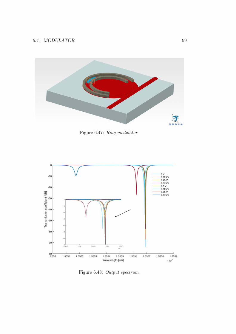
6.4. MODULATOR 99
Figure 6.47: Ring modulator
Figure 6.48: Output spectrum

100 CHAPTER 6. SIMULATION RESULTS AND DISCUSSIONS

Chapter 7
Conclusion
7.1 SummaryIn this thesis work an overview of the basic electromagnetic theory andthe main interactions between light and matter has been proposed, suchas Maxwell’s equations, light propagation, refractive index, interference, po-larization and nonlinear effects. Particular focus has been given to waveguidepropagation, starting from Snell’s law and proceeding with an outline of modepropagation, dispersion and coupling. Follows an introductory chapter aboutmodulators, in which the main parameters and modulation techniques arepresented. In particular, the phenomenon the simulation is focused on is theplasma dispersion effect (free carrier concentration variation). Subsequently,ring resonators are thoroughly explained in terms of structure, fabricationprocesses, main parameters and applications, with focus on ring modulatorswhich are the object of the thesis.
Finally, the results obtained with Lumerical and MATLAB are shown inchapter 5. First, the effective index method is used to evaluate how thisparameter changes with the structure of the waveguide. An increase of therefractive index is discovered with increasing silicon area and for higher re-fractive index claddings. The next step is the evaluation of the couplingcoefficient, which is related to the gap between the straight and bent waveg-uide and their structure. In particular, it is found to increase with longerradii and lower gaps, not to mention the presence of slabs which laterallyspread the optical pulse. Afterwards, the impact of the radius on the opticalloss has been studied. Notably, with decreasing bend radius the loss increasesdue to the overlap with the cladding. This gain is lesser for radii of morethan 5 µm, below which it starts skyrocketing.
Finally, the ring modulator is optimized taking into account different
101

102 CHAPTER 7. CONCLUSION
factors:
• First, the impact of the width of the intrinsic region is evaluated. Largewidths correspond to lower modulation capabilities but at the sametime the loss is less pronounced. The optimal value thus found is 0.6µm.
• Second, the height of the lateral slabs is considered. Bulky slabs allowa larger interaction between doped areas and optical mode and, as aresult, they are preferable in terms of modulation efficacy. However,the loss thus introduced is extremely high and therefore a trade-offheight of 70 nm has been chosen.
• Third, the optimization has been focused on the width of the lateralslabs. Longer slabs result in a minor proximity with the electric con-tacts and, as a consequence, they provide low currents and poor mod-ulations. At the same time, however, the capacitance grows due to thesheer size of the device. On the other hand, overly short slabs entail ex-ceedingly high losses and therefore cannot be taken into consideration.The optimal value has been set to 1.35 µm.
• Fourth, the doping concentration is analyzed. In particular, the dop-ing profile has been changed from constant to a more realistic diffu-sive. Low doping levels have been discarded since much improvementcould be achieved with only slightly more doped areas. However, athigh doping concentrations a flattening of the modulation efficiencybecomes clearly noticeable while the electrical properties keep steadilyworsening. The analysis of some important optical parameters has beencarried out as well. In particular, the optical spectrum becomes lessdesirable with increasing doping while parameters mainly comprisingthe refractive index variation, such as the modulation efficiency VπL,improve. Consequently, the optimal doping concentration chosen is1020 cm−3 for the regions in close proximity to the electric contacts and1018 cm−3 for the slabs in the vicinity of the optical waveguide.
• Fifth, the influence of the background doping (pepi) on the device pa-rameters is taken into account. It is found that by increasing the dopingin the intrinsic region the modulation is more effective, especially in thecase of n doping, even though the result is almost negligible comparedto other effects.
• Sixth, the behavior of the device due to different bend radii is studied.In particular, the effective index is seen to decrease with small radii

7.2. FUTURE WORKS 103
since the radiation is further overlapping with the cladding which hasa lower refractive index. Moreover, small rings display a lower losswhen not biased. It is also important to point out that, when the ringis small, there is more oscillation of the refractive index while varyingthe radius, both for the real and the imaginary part. Therefore, oncea critical dimension is reached, not much can be gained in terms ofperformance by increasing the radius.
• Lastly, a frequency analysis is carried out in order to investigate theresponse of the device at different wavelengths. Unfortunately, a mis-take has been made while fitting the material properties in Lumericaland as a result the absorption curve is plainly wrong while the groupindex shows an unrealistic resonance peak at certain frequencies. Onthe other hand, the real part of the refractive index has been fit prop-erly and shows a decrease of the refractive index and its variation withincreasing wavelength, with a steeper curve in the case of long wave-lengths.
It has been found that low voltages (even less than 1 V) are already sufficientto obtain a full modulation without jeopardizing other parameters such asER or causing an excess of current.
7.2 Future WorksIn this thesis work no attention has been paid to thermal phenomena thatusually take place in any electronic device during operation. These parasiticeffects can be detrimental for the proper behavior of the apparatus sincethey alter its electrical and optical properties. For instance, as pointed outin 4.3.4, the temperature influences directly the refractive index, leading toshifts of the output spectrum which can completely negate the modulation bydephasing the optical wavelength from the ring resonance. As a consequence,a careful analysis of the temperature dependence has to be carried out tothoroughly investigate the operation of a ring modulator.
Furthermore, in [110] the authors present a new and improved version ofequations (4.8) and (4.9), which in the case of λ0 = 1550 nm read
∆n = −5.4× 10⁻²²∆N1.011e − 1.53× 10⁻¹⁸∆N0.838
h (7.1)
∆α = 8.88× 10⁻²¹∆N1.167e + 5.84× 10⁻²⁰∆N1.109
h (7.2)

104 CHAPTER 7. CONCLUSION
Therefore, the analysis should be carried through employing these tworelations instead of the old and outdated ones in order to obtain a moreaccurate result.
Another possibility is to take advantage of the different behavior of thecarriers when it comes to light modulation (see figure 4.5) by designing asym-metric devices in order to increase the contribution of the holes in the waveg-uide. Hence, it would be possible to achieve a better and more efficient mod-ulation of the driving signal, increasing the refractive index variation andreducing the loss with respect to a traditional symmetric device.

Chapter 8
Appendix
8.1 App. A: Derivation of Gauss’ LawSome common properties of vector calculus are:
∇ · (∇× a) = 0 ∀a ∈ R3 (8.1)
∇×∇a = 0 ∀a ∈ R (8.2)
Stokes’ theorem states that (refer to figure 8.1 for a visual representation)
C
a · dl =
S
∇× a · n dS (8.3)
Where n is a versor always orthogonal to the surface S. C is a closed linethat acts as a boundary for S.
Figure 8.1: Surface S with closed boundary curve C [111]
105

106 CHAPTER 8. APPENDIX
Gauss’ theorem (divergence theorem) states that (refer to figure 8.2 for avisual representation)
S
a · n dS =
V
∇ · a dV (8.4)
Where n is a versor always orthogonal to the surface.
Figure 8.2: Volume V bounded by closed surface S [112]
Given equations (2.1) and (8.1), one can write
∇ · (∇× e(r, t)) = ∇ · (−∂b(r, t)∂t
) = − ∂
∂t(∇ · b(r, t)) = 0
Therefore we can conclude that ∇ · b(r, t) = 0. Furthermore, followingGauss’ theorem, it is
V
∇ · b(r, t) dV = 0 ⇐⇒
S
b(r, t) · n dS
Meaning that any component for which b(r, t) · n is positive is balancedby a component for which the dot product is negative. As a consequence,b(r, t) is said to be a solenoidal field whose field lines are closed [18].
Once again, because of the same property (8.1), we can write
∇ · (∇× h(r, t)) = ∇ · (∂d(r, t)
∂t+ j(r, t)) =
∂
∂t(∇ · d(r, t)) +∇ · j(r, t) = 0
Furthermore, the circulation of the current density can be written as
S
j(r, t) · n dS = −∂QV (r, t)
∂t
Where QV is the total charge contained in the volume V . Moreover,QV (r, t) =
VρV (r, t) dV is the integral of the electric charge density in the
volume, yielding (the volume is considered constant in time) [17]

8.2. APP. B: PLANE WAVE DERIVATION (GENERIC MEDIA) 107
S
j(r, t) · n dS = − ∂
∂t
V
ρV (r, t) dV = −
V
∂
∂tρV (r, t) dV
By applying (8.4) to the left side of the equation we obtain
V
∇ · j(r, t) dV =
V
− ∂
∂tρV (r, t) dV
When the volume shrinks to a point we can infer that
∇ · j(r, t) = − ∂
∂tρV (r, t)
Obtaining again equation (2.4).
8.2 App. B: Plane wave derivation (genericmedia)
A generic medium is a material for which the electrical conductivity is notnegligible (σ 6= 0) and therefore the phasor Maxwell’s equations (2.13) and(2.14) read [17]
∇× E(r) = −iωµ0H(r) (8.5)
∇× H(r) = σE(r) + iωεE(r) + J(r) = iωεcH(r) + J(r) (8.6)
Where εc = ε− iσωis called complex permittivity (accounting for losses).
Moreover, the Laplacian operator ∇2 : R3 7→ R3 is defined as
∇2a , ∇(∇ · a)−∇× (∇× a) (8.7)
We can further derive in the case of the electric field and σ 6= 0
∇× (∇× E(r)) = −iωµ0∇× H(r) = −iωµ0(iωεcE(r)) = ω2µ0εcE(r)
And
∇× (∇× E(r)) = ∇(∇ · E(r))−∇2E(r)
Where the canceled term is due to the fact that the source is not presentin the considered region of space [17].

108 CHAPTER 8. APPENDIX
Combining the two lines above, one obtains again the Helmholtz equations(2.17) and (2.18).
Furthermore, by writing
E(r) = Ex(r)x+ Ey(r)y + Ez(r)z
WithEi(r) = Ei(x, y, z) = Eoifx(x)fy(y)fz(z)
Obtained by virtue of separation of the variables, we have
∇2Ei(r) + ω2µ0εcEi(r) = 0 ∀i = x, y, z
∂2Ei(r)
∂x2+∂2Ei(r)
∂y2+∂2Ei(r)
∂z2+ ω2µ0εcEi(r) = 0
Eoi∂2fx(x)
∂x2fy(y)fz(z) +
Eoi∂2fy(y)
∂y2fx(x)fz(z) +
Eoi∂2f(z)
∂z2fx(x)fy(y)+
+ ω2µ0εcEoifx(x)fy(y)fz(z) = 0
∂2fx(x)
∂x2
1
fx(x)+∂2fy(y)
∂y2
1
fy(y)+∂2f(z)
∂z2
1
fz(z)= −ω2µ0εc
Since the right-hand term is a constant, the only possible solution is forthe three left-hand terms to be constants as well and not functions, such as
∂2fi(i)
∂i21
fi(i)= s2
i , i = x, y, z
Therefore we can state that
fi(i) = F+0ie−si·i + F−oi e
si·i
s2x + s2
y + s2z = −ω2µ0εc
With F+0i and F
−0i integration constants depending on the source.
A possible solution, called plane wave solution, is given by
Ei(r) = E0ie−sx·x−sy ·y−sz ·z = E0ie
−s·r
E(r) = E0e−s·r
As in chapter 2.1.2.

8.3. APP. C: POWER BALANCE (ELECTROMAGNETIC FIELD) 109
8.3 App. C: Power balance (electromagneticfield)
In the case of lossy media (εc = ε − iσω) and starting from equations (8.5)
and (8.6), we can write
(∇× E(r)) · H∗(r) = −iωµ0H(r) · H∗(r) (8.8)
(∇× H(r))∗ · E(r) = (σE∗(r)− iωεE∗(r) + J∗(r)) · E(r) (8.9)
Where E(r) · J∗(r) [W/m3] is the power volume density, we obtain, aftersubtracting the two equations (8.9)-(8.8)
(∇× H(r))∗ · E(r)− (∇× E(r)) · H∗(r) = σ|E(r)|2 − iωε|E(r)|2+
+ J∗(r)) · E(r) + iωµ0|H(r)|2
That is
−E(r) · J∗(r) = σ|E(r)|2 + iω(µ0|H(r)|2 − ε|E(r)|2) +∇ · (E(r)× H∗(r))
When considering a volume V and dividing by 2 to account for the powernature of the components, the relation can be written as
V
(−E(r) · J∗(r)2
) ∂V =
V
σ|E(r)|2
2∂V+iω
V
(µ0|H(r)|2
2−ε|E(r)|2
2) ∂V+
+
V
∇ · (E(r)× H∗(r)2
) ∂V
By employing relation (8.4)
V
(−E(r) · J∗(r)2
) ∂V 1 =
V
σ|E(r)|2
2∂V 2 +
+ iω
V
(µ0|H(r)|2
2− ε|E(r)|2
2) ∂V 3 +
SV
(E(r)× H∗(r)
2) · n ∂SV 4
(8.10)
Where

110 CHAPTER 8. APPENDIX
• 1 is the complex power generated by the source inside the volume;
• 2 is the power dissipation due to Joule effect (active power);
• 3 is the reactive power accumulated in the volume;
• 4 is the complex power flowing through SV (the radiated power);
The active power balance reads
Re[
V
(−E(r) · J∗(r)2
) ∂V ] =
V
σ|E(r)|2
2∂V +
SV
Re[(E(r)× H∗(r)
2)]·n ∂SV
Where the left-hand term is always positive (it is a real generator) andso is the Joule component. Consequently, the active radiated power can beeither positive or negative (depending on its relation with the surface).
The reactive power balance reads
Im[
V
(−E(r) · J∗(r)2
) ∂V ] = ω
V
(µ0|H(r)|2
2− ε|E(r)|2
2) ∂V+
+
SV
Im[(E(r)× H∗(r)
2)] · n ∂SV
Where the right-most term represents the reactive irradiated power whichdecays rapidly with the distance from the source (it is only present in theso-called near field or Fresnel region) [17].

Bibliography
[1] P. Damas, X. L. Roux, D. L. Bourdais, E. Cassan, D. Marris-Morini,N. Izard, T. Maroutian, P. Lecoeur, and L. Vivien, “Wavelength depen-dence of pockels effect in strained silicon waveguides,” Optics Express,vol. 22, p. 22095, sep 2014.
[2] A. Narasimha, B. Analui, Y. Liang, T. J. Sleboda, S. Abdalla,E. Balmater, S. Gloeckner, D. Guckenberger, M. Harrison, R. G.M. P. Koumans, D. Kucharski, A. Mekis, S. Mirsaidi, D. Song, andT. Pinguet, “A fully integrated 20-gb/s optoelectronic transceiver im-plemented in a standard 0.13 um cmos soi technology,” IEEE Journalof Solid-State Circuits, vol. 42, pp. 2736–2744, dec 2007.
[3] A. L. Lentine and C. T. DeRose, “Challenges for optical interconnectfor beyond moore's law computing,” in 2016 IEEE International Con-ference on Rebooting Computing (ICRC), IEEE, oct 2016.
[4] J. Jung, H. Nam, B. Lee, J. O. Byun, and N. S. Kim, “Fiber bragg grat-ing temperature sensor with controllable sensitivity,” Applied Optics,vol. 38, p. 2752, may 1999.
[5] H.-G. von Ribbeck, M. T. Wenzel, R. Jacob, and L. M. Eng, “Scatteringnear-field microscopy in the THz region using a free-electron laser,” in35th International Conference on Infrared, Millimeter, and TerahertzWaves, IEEE, sep 2010.
[6] A. H. Hielscher, A. Y. Bluestone, G. S. Abdoulaev, A. D. Klose,J. Lasker, M. Stewart, U. Netz, and J. Beuthan, “Near-infrared diffuseoptical tomography,” Disease Markers, vol. 18, no. 5-6, pp. 313–337,2002.
[7] W. Bogaerts, P. D. Heyn, T. V. Vaerenbergh, K. D. Vos, S. K. Sel-varaja, T. Claes, P. Dumon, P. Bienstman, D. V. Thourhout, andR. Baets, “Silicon microring resonators,” Laser & Photonics Reviews,vol. 6, pp. 47–73, sep 2011.

112 BIBLIOGRAPHY
[8] S. Spector, C. Sorace, M. Geis, M. Grein, J. Yoon, T. Lyszczarz, E. Ip-pen, and F. Kartner, “Operation and optimization of silicon-diode-based optical modulators,” IEEE Journal of Selected Topics in Quan-tum Electronics, vol. 16, no. 1, pp. 165–172, 2010.
[9] G. T. Reed, G. Mashanovich, F. Y. Gardes, and D. J. Thomson, “Siliconoptical modulators,” Nature Photonics, vol. 4, pp. 518–526, jul 2010.
[10] Q. Xu, S. Manipatruni, B. Schmidt, J. Shakya, and M. Lipson, “12.5gbit/s carrier-injection-based silicon micro-ring silicon modulators,”Optics Express, vol. 15, p. 430, jan 2007.
[11] H. Yu, D. Ying, M. Pantouvaki, J. V. Campenhout, P. Absil, Y. Hao,J. Yang, and X. Jiang, “Trade-off between optical modulation ampli-tude and modulation bandwidth of silicon micro-ring modulators,” Op-tics Express, vol. 22, p. 15178, jun 2014.
[12] W. R. McKinnon, D. X. Xu, C. Storey, E. Post, A. Densmore,A. Delâge, P. Waldron, J. H. Schmid, and S. Janz, “Extracting couplingand loss coefficients from a ring resonator,” Optics Express, vol. 17,p. 18971, oct 2009.
[13] Y. A. Vlasov and S. J. McNab, “Losses in single-mode silicon-on-insulator strip waveguides and bends,” Optics Express, vol. 12, no. 8,p. 1622, 2004.
[14] S. Kasap, Optoelectronics and Photonics: Principles and Practices.Pearson Education Limited, 2013.
[15] C. G. Someda, Electromagnetic Waves. CRC Press, 2017.
[16] G. R. Fowles, Introduction to Modern Optics (Dover Books on Physics).Dover Publications, 1989.
[17] M. Santagiustina, Antennas and Wireless Propagation. Universita degliStudi di Padova, 2018.
[18] D. De-Ceglia, Biophotonics. Universita degli Studi di Padova, 2018.
[19] P. Mazzoldi, M. Nigro, and C. Voci, Fisica vol. 2 - Elettromagnetismo,onde. Edises, 2000.
[20] “Polarization.” https://en.wikipedia.org/wiki/Polarization_(waves). Accessed: 2019-08-15.

BIBLIOGRAPHY 113
[21] S. Trippe, “Polarization and polarimetry: A review,” Journal of TheKorean Astronomical Society, 2014.
[22] “GroupIndex.” https://en.wikipedia.org/wiki/Group_velocity. Ac-cessed: 2019-08-15.
[23] “PulseTimeFrequencyRelation.” https://www.brown.edu/research/labs/mittleman/sites/brown.edu.research.labs.mittleman/files/uploads/lecture21_0.pdf. Accessed: 2019-08-15.
[24] M. Helm, Quantum Mechanics for Nanoelectronics. Technische Uni-versitaet Dresden, 2018.
[25] A. K. Ghatak, I. C. Goyal, and A. Kumar, “Propagation of a gaussianpulse through an optical fiber: applicability of geometrical optics,”Applied Optics, vol. 14, p. 2330, oct 1975.
[26] “GaussianPulse.” https://ufox.cfel.de/sites/sites_cfelgroups/site_cfel-ufox/content/e16281/e86791/e86828/e86829/e86833/2013_04_16UFSC_Lec_3.pdf. Accessed: 2019-08-15.
[27] “Interference.” https://physics.stackexchange.com/questions/107286/does-interference-take-place-only-in-waves-parallel-to-each-other.Accessed: 2019-08-15.
[28] F. Moresco, Molecular Electronics. Technische Universitaet Dresden,2018.
[29] “AtomicOrbitals.” http://www231.pair.com/fzwester/courses/bis10v/week1/13atomicorbitals.html. Accessed: 2019-08-15.
[30] M. Meneghini, Optoelectronics for Green Technologies. Universita degliStudi di Padova, 2017.
[31] “EnergyBands.” https://byjus.com/physics/what-are-energy-bands/. Accessed: 2019-08-15.
[32] C. F. Bohren and D. R. Huffman, Absorption and Scattering of Lightby Small Particles. Wiley-VCH, 1998.
[33] L. Palmieri, Optical Network Devices. Universita degli Studi di Padova,2018.
[34] D. R. Solli, P. Koonath, and B. Jalali, “Inverse raman scattering insilicon,” arXiv, 2008.

114 BIBLIOGRAPHY
[35] R. Pratt, L. LaJohn, V. Florescu, T. Surić, B. Chatterjee, and S. Roy,“Compton scattering revisited,” Radiation Physics and Chemistry,vol. 79, pp. 124–131, feb 2010.
[36] L. Rigamonti, “Schiff base metal complexes for second order nonlinearoptics,” La chimica e l’industria: rivista della societa chimica italiana,2010.
[37] R. W. Boyd, Nonlinear Optics. ACADEMIC PR INC, 2019.
[38] J. Schmiedmayer, Laseer Physics and Photonics. Universitaet Heidel-berg, 2002.
[39] M. Habibi and M. Davoodianidalik, “Self-focusing of high-power laserbeam through plasma,” in High Power Laser Systems, InTech, oct 2018.
[40] D. Mittleman, Ultrafast Optics. Brown University, 2017.
[41] R. W. Boyd, Introduction to Nonlinear Optics. International School ofPhysics "Enrico Fermi", 2014.
[42] R. Hamerly, D. Gray, C. Rogers, L. Mirzoyan, M. Namdari, andK. Jamshidi, “Optical bistability, self-pulsing and XY optimization insilicon micro-rings with active carrier removal,” in Physics and Simula-tion of Optoelectronic Devices XXV (B. Witzigmann, M. Osiński, andY. Arakawa, eds.), SPIE, feb 2017.
[43] “SnellLaw.” https://em.geosci.xyz/content/maxwell1_fundamentals/reflection_and_fraction/Snells_law.html. Accessed: 2019-08-15.
[44] P. Horak, Optical Fibres. University of Southampton, 2018.
[45] “Diffusereflection.” https://en.wikipedia.org/wiki/Diffuse_reflection. Accessed: 2019-08-15.
[46] K. Singh, “Optical fibre communication: A review,” inSingh2017OpticalFC, 2017.
[47] A. Acakpovi and P. L. M. V. Matoumona, “Comparative analysis ofplastic optical fiber and glass optical fiber for home networks,” in 2012IEEE 4th International Conference on Adaptive Science & Technology(ICAST), IEEE, oct 2012.
[48] Y. Koike and M. Asai, “The future of plastic optical fiber,” NPG AsiaMaterials, vol. 1, pp. 22–28, oct 2009.

BIBLIOGRAPHY 115
[49] S. Grassini, M. Ishtaiwi, M. Parvis, and A. Vallan, “Design and de-ployment of low-cost plastic optical fiber sensors for gas monitoring,”Sensors, vol. 15, pp. 485–498, dec 2014.
[50] “OpticalFIberCable.” https://community.fs.com/blog/the-advantages-and-disadvantages-of-optical-fibers.html. Ac-cessed: 2019-08-15.
[51] J. Kambiz, Integrated Photonic Devices. Technische Universitaet Dres-den, 2019.
[52] “OpticalFiberModes.” https://www.fiberoptics4sale.com/blogs/archive-posts/95048070-basic-optics-for-optical-fiber. Accessed:2019-08-15.
[53] “Modes.” https://www.computational-photonics.eu/oms.html. Ac-cessed: 2019-08-15.
[54] K. Okamoto, Fundamentals of Optical Waveguides (Optics & PhotonicsSeries). Academic Press, 2005.
[55] S. Spolitis and G. Ivanovs, “Realization of combined chromatic disper-sion compensation methods in high speed WDM optical transmissionsystems,” Electronics And Electrical Engineering, vol. 113, sep 2011.
[56] “ModalDispersion.” http://www.fiber-optic-cable-sale.com/what-can-limit-the-data-transmission-distance.html,.
[57] O. Heaviside, “ELECTROMAGNETIC INDUCTION AND ITSPROPAGATION (SECOND HALF.),” in Electrical Papers, pp. 39–155, Cambridge University Press, 1892.
[58] “ChromaticDispersion.” http://fobasics.blogspot.com/2012/07/chromatic-dispersion.html. Accessed: 2019-08-15.
[59] S. G. Jennings, R. G. Pinnick, and J. B. Gillespie, “Relation betweenabsorption coefficient and imaginary index of atmospheric aerosol con-stituents,” Applied Optics, vol. 18, p. 1368, may 1979.
[60] R. Corvaja, Optical and Quantum Communications. Universita degliStudi di Padova, 2017.
[61] G. Ghione, Semiconductor Devices for High-Speed Optoelectronics.Cambridge University Press, 2009.

116 BIBLIOGRAPHY
[62] K. Daikoku, “Direct modulation characteristics of semiconductor laserdiodes,” Japanese Journal of Applied Physics, vol. 16, pp. 117–124, jan1977.
[63] S. Warm, Electronic Predistortion Strategies For Directly ModulatedLaser Systems. Technische Universitaet Berlin, 2009.
[64] M. Berciano, G. Marcaud, P. Damas, X. L. Roux, P. Crozat, C. A.Ramos, D. P. Galacho, D. Benedikovic, D. Marris-Morini, E. Cassan,and L. Vivien, “Fast linear electro-optic effect in a centrosymmetricsemiconductor,” Communications Physics, vol. 1, oct 2018.
[65] B. Chmielak, M. Waldow, C. Matheisen, C. Ripperda, J. Bolten,T. Wahlbrink, M. Nagel, F. Merget, and H. Kurz, “Pockels effect basedfully integrated, strained silicon electro-optic modulator,” Optics Ex-press, vol. 19, p. 17212, aug 2011.
[66] Y. Turkulets and I. Shalish, “Franz-keldysh effect in semiconductorbuilt-in fields: Doping concentration and space charge region charac-terization,” Journal of Applied Physics, vol. 124, p. 075102, aug 2018.
[67] R. S. Jacobsen, K. N. Andersen, P. I. Borel, J. Fage-Pedersen, L. H.Frandsen, O. Hansen, M. Kristensen, A. V. Lavrinenko, G. Moulin,H. Ou, C. Peucheret, B. Zsigri, and A. Bjarklev, “Strained silicon as anew electro-optic material,” Nature, vol. 441, pp. 199–202, may 2006.
[68] C. Schriever, C. Bohley, J. Schilling, and R. B. Wehrspohn, “Strainedsilicon photonics,” Materials, vol. 5, pp. 889–908, may 2012.
[69] R. Soref and B. Bennett, “Electrooptical effects in silicon,” IEEE Jour-nal of Quantum Electronics, vol. 23, pp. 123–129, jan 1987.
[70] A. Irace, G. Breglio, M. Iodice, and A. Cutolo, “Light modulation withsilicon devices,” in Topics in Applied Physics, pp. 361–391, SpringerBerlin Heidelberg, feb 2004.
[71] D. Marris-Morini, L. Vivien, and G. Rasigade, Optical Modulators inSilicon Photonic Circuits. Institut d-Electronique Fondamentale - Uni-versite Paris Sud, 2009.
[72] G. Cocorullo, F. G. D. Corte, and I. Rendina, “Temperature depen-dence of the thermo-optic coefficient in crystalline silicon between roomtemperature and 550 k at the wavelength of 1523 nm,” Applied PhysicsLetters, vol. 74, pp. 3338–3340, may 1999.

BIBLIOGRAPHY 117
[73] J. Fage-Pedersen, L. Frandsen, A. Lavrinenko, and P. Borel, “A linearelectrooptic effect in silicon, induced by use of strain,” in 3rd IEEEInternational Conference on Group IV Photonics, 2006., IEEE, 2006.
[74] Y. Varshni, “Temperature dependence of the energy gap in semicon-ductors,” Physica, vol. 34, pp. 149–154, jan 1967.
[75] Z. Zhang, Silicon-based Photonic Devices: Design, Fabrication andCharacterization. PhD thesis, KTH Royal Institute of Technology,2008.
[76] A. Yariv, “Critical coupling and its control in optical waveguide-ring resonator systems,” IEEE Photonics Technology Letters, vol. 14,pp. 483–485, apr 2002.
[77] G. Mashanovic, Introduction to Silicon Photonics. University ofSouthampton, 2018.
[78] K. D. Vos, Label-free Silicon Photonics Biosensor Platform with Mi-croring Resonator. PhD thesis, Universiteit Gent, 2010.
[79] H. Qing-Zhong, Y. Jin-Zhong, C. Shao-Wu, X. Xue-Jun, H. Wei-Hua,and F. Zhong-Chao, “Design, fabrication and characterization of ahigh-performance microring resonator in silicon-on-insulator,” ChinesePhysics B, vol. 17, pp. 2562–2566, jul 2008.
[80] “Photolitoghraphy.” http://toppicture.dx.am/?top=3&definitions=Photolithography. Accessed: 2019-08-15.
[81] J. Tian and M. Qiu, “Micro-ring resonators fabricated by focused-ion-beam on SOI,” in Optical Transmission, Switching, and Subsystems VI(K. ichi Kitayama, P. C. Ghiggino, K. Roberts, and Y. Su, eds.), SPIE,nov 2008.
[82] B. A. Joyce, “Molecular beam epitaxy,” Reports on Progress in Physics,vol. 48, pp. 1637–1697, dec 1985.
[83] T. Mikolajick, Innovative Semiconductor Devices. Technische Univer-sitaet Dresden, 2018.
[84] S. Beebly, Microsensor Technologies. University of Southampton, 2018.
[85] A. Samarelli, Micro Ring Resonators in Silicon-on-Insulator. PhD the-sis, University of Glasgow, 2011.

118 BIBLIOGRAPHY
[86] U. W. Pohl, “Doping, diffusion, and contacts,” in Graduate Texts inPhysics, pp. 225–273, Springer Berlin Heidelberg, 2013.
[87] L. N. Large and R. W. Bicknell, “Ion-implantation doping of semicon-ductors,” Journal of Materials Science, vol. 2, pp. 589–609, nov 1967.
[88] “RefractiveIndex.” https://refractiveindex.info/. Accessed: 2019-08-15.
[89] S. Tanaka, T. Usuki, and Y. Tanaka, “Accurate SPICE model offorward-biased silicon PIN mach zehnder modulator for an energy-efficient multilevel transmitter,” Journal of Lightwave Technology,vol. 36, pp. 1959–1969, may 2018.
[90] W. Bogaerts, R. Baets, P. Dumon, V. Wiaux, S. Beckx, D. Tail-laert, B. Luyssaert, J. V. Campenhout, P. Bienstman, and D. V.Thurnout, “Nanophotonic waveguides in silicon-on-insulator fabricatedwith CMOS technology,” Journal of Lightwave Technology, vol. 23,pp. 401–412, jan 2005.
[91] A. S. Jensen, Fabrication and Characterisation of Silicon Waveguidesfor High-Speed Optical Signal Processing. PhD thesis, Technical Uni-versity of Denmark, 2015.
[92] A. Shutler, “Investigation of propagation loss of passive silicon waveg-uides using two different etching techniques,” NNIN REU ResearchAccomplishments, 2008.
[93] D. Taillaert, W. V. Paepegem, J. Vlekken, and R. Baets, “A thin foiloptical strain gage based on silicon-on-insulator microresonators,” inThird European Workshop on Optical Fibre Sensors, SPIE, jul 2007.
[94] H.-T. Kim and M. Yu, “Cascaded ring resonator-based temperaturesensor with simultaneously enhanced sensitivity and range,” Optics Ex-press, vol. 24, p. 9501, apr 2016.
[95] K. D. Vos, I. Bartolozzi, E. Schacht, P. Bienstman, and R. Baets,“Silicon-on-insulator microring resonator for sensitive and label-freebiosensing,” Optics Express, vol. 15, no. 12, p. 7610, 2007.
[96] “Biosensing.” http://photonics.deib.polimi.it/biosensing/. Ac-cessed: 2019-08-15.
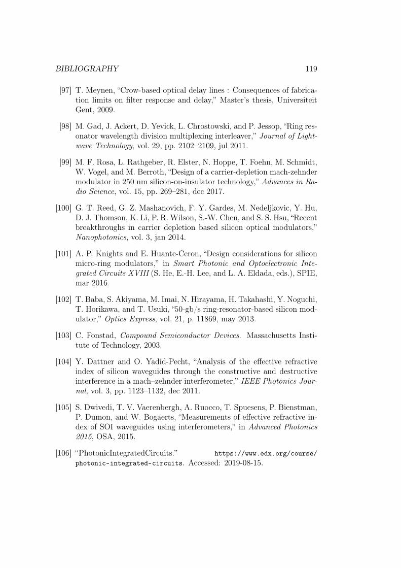
BIBLIOGRAPHY 119
[97] T. Meynen, “Crow-based optical delay lines : Consequences of fabrica-tion limits on filter response and delay,” Master’s thesis, UniversiteitGent, 2009.
[98] M. Gad, J. Ackert, D. Yevick, L. Chrostowski, and P. Jessop, “Ring res-onator wavelength division multiplexing interleaver,” Journal of Light-wave Technology, vol. 29, pp. 2102–2109, jul 2011.
[99] M. F. Rosa, L. Rathgeber, R. Elster, N. Hoppe, T. Foehn, M. Schmidt,W. Vogel, and M. Berroth, “Design of a carrier-depletion mach-zehndermodulator in 250 nm silicon-on-insulator technology,” Advances in Ra-dio Science, vol. 15, pp. 269–281, dec 2017.
[100] G. T. Reed, G. Z. Mashanovich, F. Y. Gardes, M. Nedeljkovic, Y. Hu,D. J. Thomson, K. Li, P. R. Wilson, S.-W. Chen, and S. S. Hsu, “Recentbreakthroughs in carrier depletion based silicon optical modulators,”Nanophotonics, vol. 3, jan 2014.
[101] A. P. Knights and E. Huante-Ceron, “Design considerations for siliconmicro-ring modulators,” in Smart Photonic and Optoelectronic Inte-grated Circuits XVIII (S. He, E.-H. Lee, and L. A. Eldada, eds.), SPIE,mar 2016.
[102] T. Baba, S. Akiyama, M. Imai, N. Hirayama, H. Takahashi, Y. Noguchi,T. Horikawa, and T. Usuki, “50-gb/s ring-resonator-based silicon mod-ulator,” Optics Express, vol. 21, p. 11869, may 2013.
[103] C. Fonstad, Compound Semiconductor Devices. Massachusetts Insti-tute of Technology, 2003.
[104] Y. Dattner and O. Yadid-Pecht, “Analysis of the effective refractiveindex of silicon waveguides through the constructive and destructiveinterference in a mach–zehnder interferometer,” IEEE Photonics Jour-nal, vol. 3, pp. 1123–1132, dec 2011.
[105] S. Dwivedi, T. V. Vaerenbergh, A. Ruocco, T. Spuesens, P. Bienstman,P. Dumon, and W. Bogaerts, “Measurements of effective refractive in-dex of SOI waveguides using interferometers,” in Advanced Photonics2015, OSA, 2015.
[106] “PhotonicIntegratedCircuits.” https://www.edx.org/course/photonic-integrated-circuits. Accessed: 2019-08-15.

120 BIBLIOGRAPHY
[107] Q. Xu, B. Schmidt, S. Pradhan, and M. Lipson, “Micrometre-scalesilicon electro-optic modulator,” Nature, vol. 435, pp. 325–327, may2005.
[108] “OpticalBands.” https://www.fiberlabs.com/glossary/about-optical-communication-band/. Accessed: 2019-08-15.
[109] K. Debnath, D. J. Thomson, W. Zhang, A. Z. Khokhar, C. Littlejohns,J. Byers, L. Mastronardi, M. K. Husain, K. Ibukuro, F. Y. Gardes,G. T. Reed, and S. Saito, “All-silicon carrier accumulation modulatorbased on a lateral metal-oxide-semiconductor capacitor,” Photonics Re-search, vol. 6, p. 373, apr 2018.
[110] M. Nedeljkovic, R. Soref, and G. Z. Mashanovich, “Free-carrier elec-trorefraction and electroabsorption modulation predictions for siliconover the 1-14- µm infrared wavelength range,” IEEE Photonics Journal,vol. 3, pp. 1171–1180, dec 2011.
[111] “StokesOnline.” http://tutorial.math.lamar.edu/Classes/CalcIII/StokesTheorem.aspx. Accessed: 2019-08-15.
[112] “Divergence.” https://en.wikipedia.org/wiki/Divergence_theorem.Accessed: 2019-08-15.