department of electronics & telecommunication · pdf filedepartment of electronics &...
TRANSCRIPT

S.E. (E&TC)-Semester-IV Page 1
Department of Electronics & Telecommunication Engineering
Second Year Engineering
Semester – III
Course Structure
Sr. No. Subject
Teaching Scheme
(Hrs)
Examination Scheme
(Marks)
L T P Total Theory TW POE OE Total
1 Analog Circuits -II 4 -- 2 6 100 25 50 -- 175
2 Linear Integrated Circuits 4 -- 2 6 100 25 50 -- 175
3 Data Structure 3 -- 2 5 100 25 -- -- 125
4 Electromagnetic Engineering 4 1 -- 5 100 25 -- -- 125
5 Analog Communication Systems 4 -- 2 6 100 25 -- 50 175
6 Circuit Simulation -- -- 2 2 -- 25 -- -- 025
7 Total 19 1 10 30 500 150 100 50 800
Index
Sr. No. Subject Subject code Page No.
1 Analog Circuits -II ETC207 02
2 Linear Integrated Circuits ETC208 15
3 Data Structure ETC209 29
4 Electromagnetic Engineering ETC210 42
5 Analog Communication Systems ETC211 51
6 Circuit Simulation ETC212 62
S.E. (E&TC)-Semester-IV Page 2
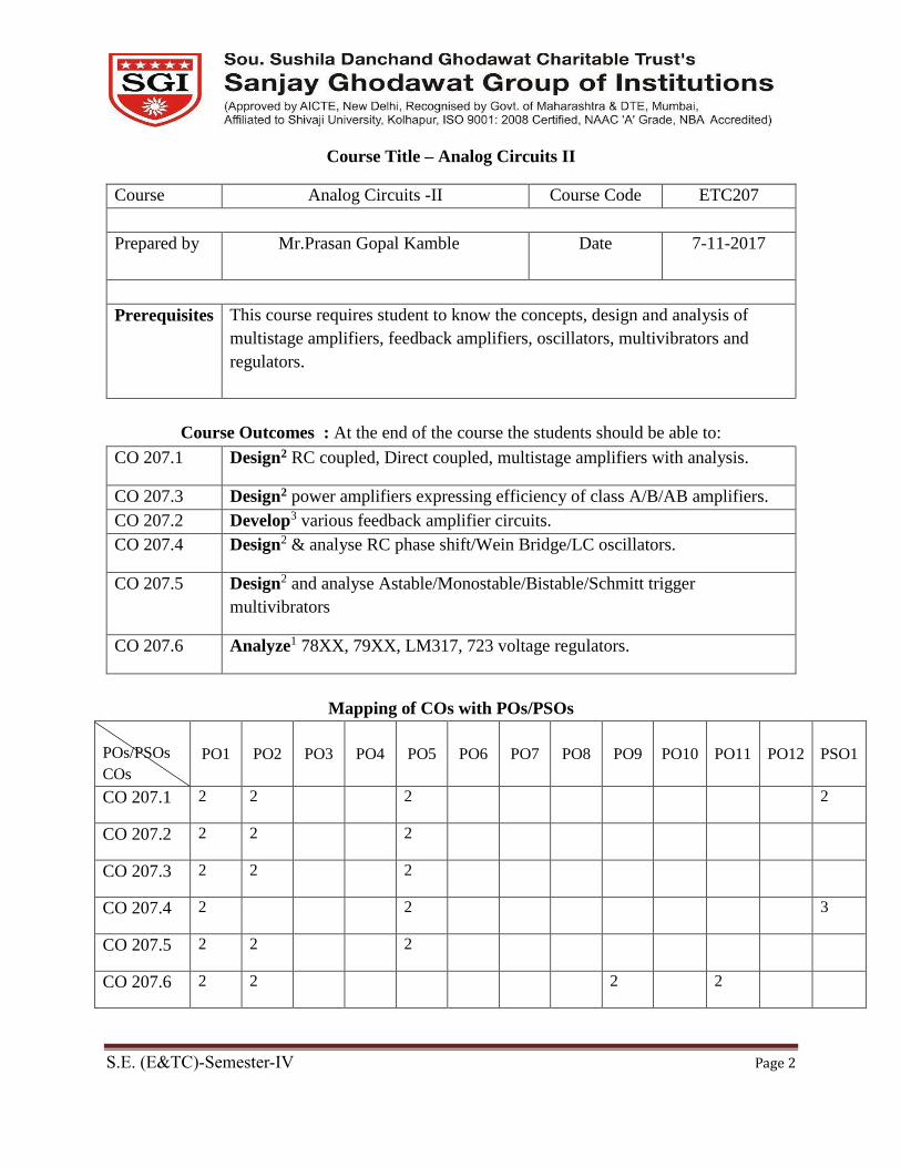
Course Title – Analog Circuits II
Course Analog Circuits -II Course Code ETC207
Prepared by Mr.Prasan Gopal Kamble
Date 7-11-2017
Prerequisites This course requires student to know the concepts, design and analysis of
multistage amplifiers, feedback amplifiers, oscillators, multivibrators and
regulators.
.
Course Outcomes : At the end of the course the students should be able to:
CO 207.1 Design2 RC coupled, Direct coupled, multistage amplifiers with analysis.
CO 207.3 Design2 power amplifiers expressing efficiency of class A/B/AB amplifiers.
CO 207.2 Develop3 various feedback amplifier circuits.
CO 207.4 Design2 & analyse RC phase shift/Wein Bridge/LC oscillators.
CO 207.5 Design2 and analyse Astable/Monostable/Bistable/Schmitt trigger
multivibrators
CO 207.6 Analyze1 78XX, 79XX, LM317, 723 voltage regulators.
Mapping of COs with POs/PSOs
POs/PSOs
COs
PO1 PO2 PO3 PO4 PO5 PO6 PO7 PO8 PO9 PO10 PO11 PO12 PSO1
CO 207.1 2 2 2 2
CO 207.2 2 2 2
CO 207.3 2 2 2
CO 207.4 2 2 3
CO 207.5 2 2 2
CO 207.6 2 2 2 2
S.E. (E&TC)-Semester-IV Page 3
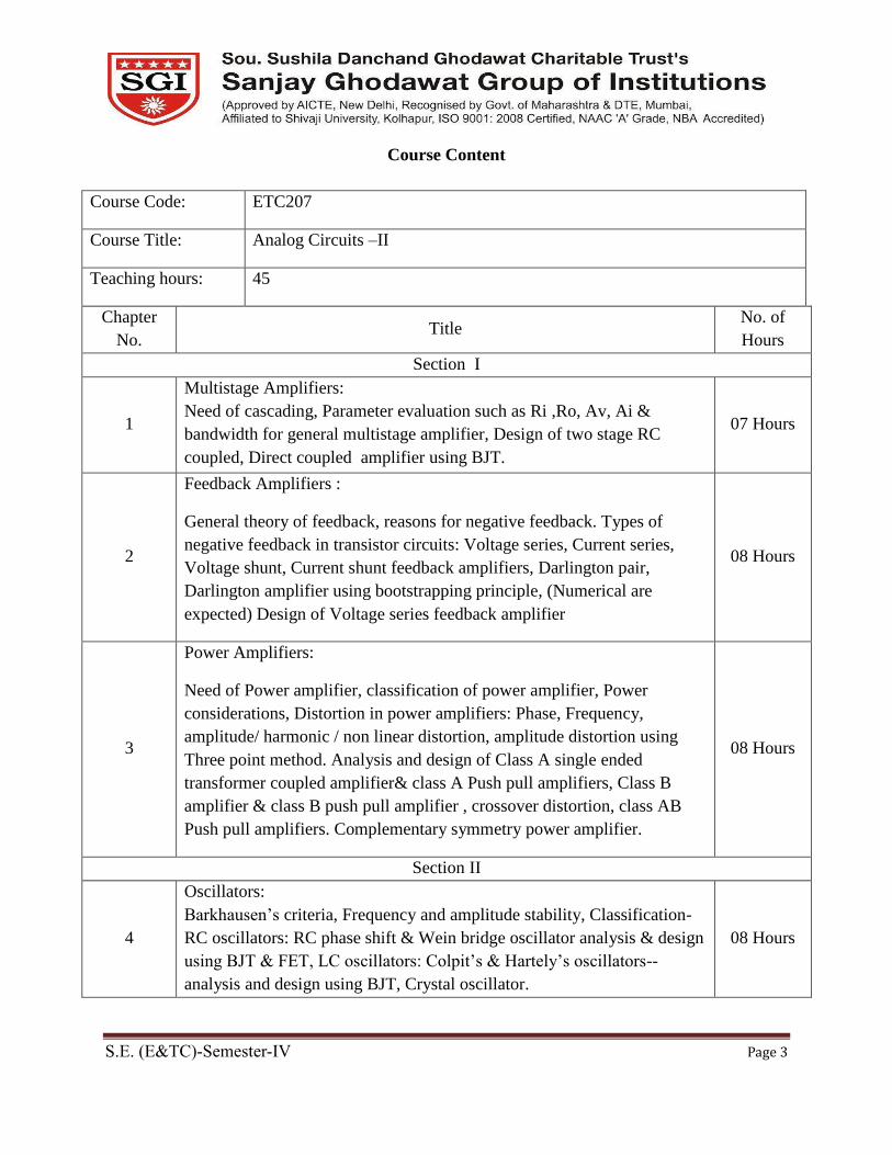
Course Content
Course Code: ETC207
Course Title: Analog Circuits –II
Teaching hours: 45
Chapter
No. Title
No. of
Hours
Section I
1
Multistage Amplifiers:
Need of cascading, Parameter evaluation such as Ri ,Ro, Av, Ai &
bandwidth for general multistage amplifier, Design of two stage RC
coupled, Direct coupled amplifier using BJT.
07 Hours
2
Feedback Amplifiers :
General theory of feedback, reasons for negative feedback. Types of
negative feedback in transistor circuits: Voltage series, Current series,
Voltage shunt, Current shunt feedback amplifiers, Darlington pair,
Darlington amplifier using bootstrapping principle, (Numerical are
expected) Design of Voltage series feedback amplifier
08 Hours
3
Power Amplifiers:
Need of Power amplifier, classification of power amplifier, Power
considerations, Distortion in power amplifiers: Phase, Frequency,
amplitude/ harmonic / non linear distortion, amplitude distortion using
Three point method. Analysis and design of Class A single ended
transformer coupled amplifier& class A Push pull amplifiers, Class B
amplifier & class B push pull amplifier , crossover distortion, class AB
Push pull amplifiers. Complementary symmetry power amplifier.
08 Hours
Section II
4
Oscillators:
Barkhausen’s criteria, Frequency and amplitude stability, Classification-
RC oscillators: RC phase shift & Wein bridge oscillator analysis & design
using BJT & FET, LC oscillators: Colpit’s & Hartely’s oscillators--
analysis and design using BJT, Crystal oscillator.
08 Hours

S.E. (E&TC)-Semester-IV Page 4
5
Multivibrators :
Transistor as a switch, Different transistor switching parameters,
overdrive factor, classification of multivibrators, Analysis and design of
collector coupled -Astable, Monostable, fixed bias and self bias Bistable
multivibrator and Schmitt trigger using BJT considering overdrive factor.
Triggering circuits for Multivibrators
08 Hours
6
IC Voltage regulator:
Study and design of regulators using IC’s :78XX, 79XX,LM723,LM317
Switching regulator LM3524
06 Hours
Reference Books:
Sr. No. Title of Book Author Publisher/Edition Topics
1 Electronic devices & circuits-
Allen Mottershed Edition-Tata
McGraw Hill
Publication
1,2,,3,5,6
2 A Monograph on Electronics
design principles
N.C.Goyal &
.K.Khetan
V Edition-
Khanna
2,3,5,6
3 Electronic devices & circuits S Salivahanan N
Sureshkumar
Tata McGraw
Hill Publication
1,2,3,4,5
4 Electronic devices & circuit
theory
RobertL.Boylsted,Louis
Nashelsky
Pearson
Education
2,3,4,5
5 National Semiconductor
Data Manual.
Examination
Scheme
Theory Term Work POE Total
Max. Marks 100 25 50 175
Contact
Hours/ week
4 2 -- 6

S.E. (E&TC)-Semester-IV Page 5
Scheme of Marks
Section Unit No. Title Marks
I
I Multistage Amplifiers 16
II Feedback Amplifiers 16
III Power Amplifiers 18
II
IV Oscillators 20
V Multivibrators 20
VI IC Voltage regulator 10
Course Unitization
Section
Unit Course
Outcomes
No. of Questions in
No. Title CAT-I CAT-II CAT-III
I 1 Multistage Amplifiers CO 207.1 02
2 Feedback Amplifiers CO 207.2 02
3 Power Amplifiers CO 207.3 02
II 4 Oscillators CO 207.4 02
5 Multivibrators CO 207.5 02
6 Voltage regulators CO 207.6 01
Unit wise Lesson Plan
Section I
Unit
No
01 Unit Title Multistage Amplifiers Planned
Hrs.
07

S.E. (E&TC)-Semester-IV Page 6
Lesson schedule
Class
No.
Details to be covered
1 Block diagram of multistage amplifier and need for cascading
2 Parameter evaluation of Ri,Ro,Av,Ai of a general multistage amplifier
3 Operation,frequency response of two stage RC coupled amplifier and Direct coupled amplifier
4 Analysis of RC coupled amplifier and numericals
5 Analysis of direct coupled amplifier and numericals
Review Questions
Q1 Explain two stage Direct coupled amplifier and draw its frequency
response
CO 207.1
Q2 Derive expression for Ri, Ro, Av, Ai of two stage RC coupled amplifier CO 207.1
Q3 Explain the need of cascading CO 207.1
Q4 Determine Av, Ai, Zi, Zo of Two stage RC coupled amplifier if hie=1k,
hfe=45, hre=250µ, hoe=25µA/v R1=91k, R2=100k, RC=150k, RE=20k,
Vcc=16v.
CO 207.1
Q5 Design two stage RC coupled amplifier for the following specification,
Vcc=16v, hfe=110, VCE=45v, PDt=450mW, IC=4mA.
CO 207.1
Q6 Give comparison between RC coupled/Direct coupled/Transformer
coupled amplifier
CO 207.1
Unit
No
02 Unit Title Feedback Amplifiers Planned
Hrs.
08
Lesson schedule
Class
No.
Details to be covered
S.E. (E&TC)-Semester-IV Page 7
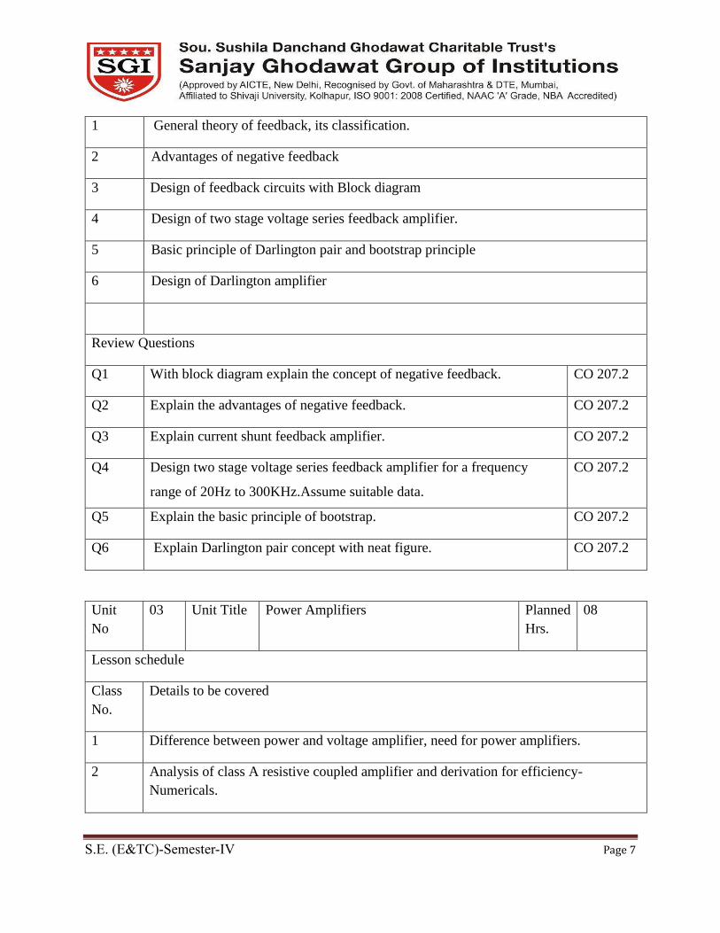
1 General theory of feedback, its classification.
2 Advantages of negative feedback
3 Design of feedback circuits with Block diagram
4 Design of two stage voltage series feedback amplifier.
5 Basic principle of Darlington pair and bootstrap principle
6 Design of Darlington amplifier
Review Questions
Q1 With block diagram explain the concept of negative feedback. CO 207.2
Q2 Explain the advantages of negative feedback. CO 207.2
Q3 Explain current shunt feedback amplifier. CO 207.2
Q4 Design two stage voltage series feedback amplifier for a frequency
range of 20Hz to 300KHz.Assume suitable data.
CO 207.2
Q5 Explain the basic principle of bootstrap. CO 207.2
Q6 Explain Darlington pair concept with neat figure. CO 207.2
Unit
No
03 Unit Title Power Amplifiers Planned
Hrs.
08
Lesson schedule
Class
No.
Details to be covered
1 Difference between power and voltage amplifier, need for power amplifiers.
2 Analysis of class A resistive coupled amplifier and derivation for efficiency-
Numericals.

S.E. (E&TC)-Semester-IV Page 8
3 Analysis of class A transformer coupled amplifier and derivation for efficiency-
Numericals.
4 Analysis of class B amplifier and derivation for efficiency, push pull amplifier-
Numericals.
5 Analysis of class B complementary symmetry push pull amplifier-numericals.
6 Analysis of class AB amplifiers-cross over distortion.
7 Phase/harmonic/frequency/amplitude/three point method distortion.
Review Questions
Q1 In a class A amplifier VCEmax=15v, VCEmin=1v Find efficiency of resistive
and transformer coupled
CO 207.3
Q2 Derive expression for power and efficiency of class B power amplifier. CO 207.3
Q3 Explain cross over distortion. How is it eliminated? CO 207.3
Q4 A class A power amplifier has zero signal power dissipation of 10W.If ac
output power is 4W, find efficiency and power rating of transistor.
CO 207.3
Q5 A class A power amplifier is supplied with 10v.If collector current is
100mA, find power transferred to a 4Ω load, if load is transformer
coupled.
CO 207.3
Q6 Explain complementary symmetry push pull amplifiers CO 207.3
Q7 Explain three point method of second harmonic distortion. CO 207.3
Unit
No
04 Unit Title Oscillators Planned
Hrs.
08
Lesson schedule
Class
No.
Details to be covered
1 Block diagram of oscillator, Barkhausen,s criteria and feedback in oscillators .
2 Classification of oscillators, design and analysis of RC phase shift oscillator/Wein
Bridge.

S.E. (E&TC)-Semester-IV Page 9
3 Design and analysis of Hartley oscillator/Collipits oscillator -Numericals
4 Amplitude & frequency stability
5 Numericals
6 Operation of crystal oscillator-series and parallel resonant circuit
Review Questions
Q1 Derive expression for frequency of oscillation of Hartley oscillator. CO 207.4
Q2 Derive expression for frequency of oscillation of Wein bridge oscillator. CO 207.4
Q3 Derive expression β=23+29R/RC+4RC/R of RC phase shift oscillator. CO 207.4
Q4 Derive expression for series and parallel resonance of crystal.. CO 207.4
Q5 Design a Wein bridge oscillator for the following
specification,hfe=200,IE=1.5mA,S=8,Vcc=12v,fo=500Hz
CO 207.4
Q6 Design a Hartley oscillator for the following
specification,hfe=200,IE=1.5mA,S=8,Vcc=12v,fo=500KHz
CO 207.4
Q7 Write short notes on Frequency and amplitude stability. CO 207.4
Unit
No
05 Unit Title Multivibrators Planned
Hrs.
08
Lesson schedule
Class
No.
Details to be covered
1 Transistor as a switch & switching parameters.
2 Classification of multivibrators.
3 Design,operation and analysis of Astable multivibrator -Numericals.

S.E. (E&TC)-Semester-IV Page 10
4 Design, operation and analysis of Monostable multivibrator -Numericals..
5 Design, operation and analysis of Bistable multivibrator -Numericals.
6 Design, operation and analysis of Schmitt trigger-Numericals.
7 Triggering circuits for multivibrators.
8 Numericals.
Review Questions
Q1 Design Monostable Multivibrator for following specification, T=140µs,
hfe=20,Icsat=6mA,Vcc=6v,VBB=-1.5v.
CO 207.5
Q2 Explain unsymmetrical and symmetrical triggering. CO 207.5
Q3 Design Bistable Multivibrator for following specification,RC1=RC2=2.2k
,hfe=20, ,Vcc=12v,VBB=-12v,R1=R2=15k,R3=R4=100k
CO 207.5
Q4 Design a Schmitt trigger circuit to have
Vcc=12v,UTP=5v,LTP=3v,Ic=2mA,hfe=100,I2=0.1Ic2
CO 207.5
Q5 Explain with waveform the operation of monostable multivibrator. CO 207.5
Q6 Explain advantages of Bistable multivibrators CO 207.5
Q7 Explain how transistor works as a switch. CO 207.5
Unit
No
06 Unit Title IC Regulators Planned
Hrs.
06
Lesson schedule
Class
No.
Details to be covered
1 Classification of IC regulators,viz.78XX/79XX/723/317
2 Design of fixed 78XX & 79XX IC regulators.
3 Design, operation and analysis of 723 regulator-Numericals.

S.E. (E&TC)-Semester-IV Page 11
4 Design, operation and analysis of LM 317 regulator-Numericals.
5 Study of LM3524 regulator
Review Questions
Q1 Design a power supply to provide a fixed voltage of -12v using IC
regulator.
CO 207.6
Q2 Explain operation of 723 voltage regulator. CO 207.6
Q3 Explain pin configuration of 723 voltage regulator CO 207.6
Q4 Write short note on switching regulator. CO 207.6
Q5 Design a voltage regulator using IC 723 for Vo=5v &
IL=80mA.Assume Vsense=0.7v
CO 207.6
Q6 Explain fold back current limiting. CO 207.6
Q7 Explain features of LM 3524 regulator CO 207.6
Model Question Paper
Course Title : ANALOG CIRCUITS-II
Duration: 3 Hours 100
Instructions: 1. All questions are compulsory.
2. Assume missing data wherever necessary.
3. Non programmable calculators are allowed.
4. Use of data sheet is allowed.
Section-I
Answer any two of the following. Marks
1 a Explain current series feedback amplifier circuit. 9
b Compare voltage series and current series feedback amplifier 9
c Explain Darlington amplifier circuit with neat circuit diagram. 9

S.E. (E&TC)-Semester-IV Page 12
2 Answer any two of the following.
a Design a two stage RC coupled amplifier for the following
specifications,hfe1=hfe2=180,RL=1k,IE1=IE2=1mA,S=3,Vcc=12v,f=
100Hz
8
b Derive expression for current gain, voltage gain, and input impedance
of direct coupled amplifier.
8
c Derive expression for power and collector efficiency of class A
transformer coupled amplifier
8
3 Answer any two of the following
a Explain three point method of second harmonic distortion 8
b Explain 723 voltage regulator circuit 8
c Compare 78XX, 79XX and 723 voltage regulators in terms of
specifications.
8
Section-II
4 Answer any two of the following Marks
a Design a Collipits oscillator for the following,
specifications,C1=0.1µF,L=1mH, f=800kHz,Vcc=12v
8
b Show that β= 23+29R/RC+4RC/R of RC phase shift oscillator. 8
c Derive expression for series and parallel resonance of crystal. 8
5
Answer any two of the following
a Design a Schmitt trigger circuit to have
Vcc=12v,UTP=5v,LTP=3v,Ic=2mA,hfe=100,I2=0.1Ic2
8
b Explain collector coupled Astable multivibrator with waveforms. 8
c Design Monostable Multivibrator for following specification, T=120µs,
hfe=50, Icsat=4mA,Vcc=6v,VBB=-1.5v.
8
6 Write short notes on any three of the following

S.E. (E&TC)-Semester-IV Page 13
a Bistable multivibrator 6
b Crystal oscillator 6
c Triggering circuits for multivibrator 6
d LM 317 regulator 6
Assignments
List of experiments/assignments to meet the requirements of the syllabus
Assignment No. 1 207.1/207.2
1. Explain the operation of two stage direct coupled amplifier circuit.
2. Design a two stage RC coupled amplifier for the following specifications.
RL=3KΩ,Rs=600Ω,Vo=9Vpp,Vcc=15v lower 3dB frequency=50Hz.
3. Classify different types of two stage amplifiers.
4. Explain frequency response of RC coupled amplifier in detail.
5. Derive expression for AVF and Zif for current shunt feedback amplifier.
6. Calculate a) Avf b)Rif c)ROf of a voltage series feedback amplifier if
Rs=600Ω,RL=2kΩ,hfe=80,hie=5k
7. Explain bootstrapped darlington pair circuit.
Assignment No. 2 207.3/207.4
1. Design a transformer coupled class A amplifier with Po=2W across 4Ω load with 70%
efficiency of transformer.Assume Vcc=12v, hfe=120.
2. Derive expression for power and efficiency of class direct coupled amplifier.
3. Give comparison between voltage and power amplifiers.
4. Explain cross over distortion in amplifiers.
5. Explain three point method of harmonic distortion calculation.
6. Design RC phase shift oscillator circuit with fo=100kHz,VCEQ=5v,ICQ=5mA,Vcc=15v,
hfe=100,hie=1kΩ,VBE=0.6v.
7. Design a Hartley oscillator for Vo=4vrms, RL=2.2kΩ,fo=5MHz.
8. Derive expression for fo of Collipits oscillator.
9. Derive expression for series and parallel resonance of crystal.
Assignment No. 3 207.5/207.6
1.Explain design procedure for Monostable Multivibrator for generating pulse of required
Duration and magnitude.

S.E. (E&TC)-Semester-IV Page 14
2. With waveform diagram explain the operation of Astable multivibrator.
3.Design Schmitt trigger circuit for the given data,UTP=3v,LTP=1.5v,Vcc=15v,IC(Sat)=5mA,
hfe=40.
4.Design a Monostable multivibrator for the following specifications: Output pulse width
=1ms,Vcc=10v,VBB=5v,VBE(sat)=0.6v,VCE(sat)=0.3v,Icsat=5mA,hfe=200,Icmax
=0.1A, VCEmax=45v, PDmax=0.5W.
5. Compare linear regulators (723) and SMPS (LM3524).
6. Explain IC voltage regulators.
Lab Plan
Experiment No Experiment Title CO
1 Design & Frequency response of direct coupled amplifier. CO 207.1
2 Design & Frequency response of two stage RC coupled
amplifier. CO 207.1
3 Design & Frequency response of voltage series feedback
amplifier. CO 207.2
4 Design of transformer coupled class A amplifier. CO 207.3
5 Design of RC phase shift oscillator using BJT. CO 207.4
6 Design of wein bridge oscillator using BJT. CO 207.4
7 Design of colpitts oscillator using BJT. CO 207.4
8 Design of hartley oscillator using BJT. CO 207.4
9 Design of Astable multivibrator. CO 207.5
10 Design of monostable multivibrator using BJT. CO 207.5
11 Design of bistable multivibrator using BJT. CO 207.5
12 Design of Schmitt trigger using BJT. CO 207.5
13 Design of voltage regulator using LM317. CO 207.6
14 Design of voltage regulator using IC723. CO 207.6

S.E. (E&TC)-Semester-IV Page 15
Course Title – Linear Integrated Circuits
Course LIC Course Code ETC208
Prepared by Mr.M.P.Mattada, Mrs. Shinde P P, Date 4/11/2017
Prerequisites To learn basic of Integrated Circuits with theoretical and practical knowledge
in simplified form to analyze and design wide variety of OP-AMP circuits,
linear and non-linear Integrated Circuits to perform desired operations.
Course Outcomes : At the end of the course the students should be able to;
CO208.1 Define1 various Operational/Differential amplifier characteristics, circuit
design consideration using analogue monolithic IC’s such as IC 741, CA3140.
CO208.2 Identify1 and draw Op-amp configurations, frequency response and
compensation techniques.
CO208.3 Demonstrate2 knowledge of basic linear and non-linear applications of OP-
AMP by solving differential equations and design oriented numerical.
CO208.4 Classify2 and Design5 of different types of active filters.
CO208.5 Compute5 component values to design different Op-amp based circuits which
include arithmetic building blocks, waveform generators, Oscillators etc.
CO208.6 Explain1 the working of various circuits for different applications designed
using linear integrated circuits such as IC555, IC566 and IC565.
Mapping of COs with POs
PSO1
POs
COs
PO1
PO2 PO3 PO4 PO5 PO6 PO7 PO8 PO9 PO10 PO11 PO12 PS01
CO208.1 1 2 2
CO208.2 1 2 2
CO208.3 3 2 2 2
CO208.4 2 2 2 2
CO208.5 2 2 2 2
CO208.6 2 2 2 2

S.E. (E&TC)-Semester-IV Page 16
Course Contents
Unit No. Title No. of
Hours
Section I
1.
Introduction to op-amp:
Introduction to op-amp: definition, symbol, block diagram, ideal
characteristics of Op-amp, AC & DC analysis of dual input balanced
output type differential amplifier. Comparative study of other
configurations of differential amplifiers, Analysis of typical op-amp,
equivalent circuit, op-amp parameters, equivalent circuit of op-amp,
study of IC 741, CA3140.
09
2.
Op-amp configurations & frequency response:
Open loop configuration, closed loop configurations, frequency
Response, Stability considerations, Frequency Compensation, Slew
Rate.
07
3.
Applications of Op-amp:
Summing, Scaling & Averaging Amplifiers using Op-amps,
Differential amplifier using opamp, Subtract or Circuit,
Instrumentation amplifier, V to I & I to V Converter, Precision
Rectifiers, Log & Anti-log Amplifiers, Study of comparator, Schmitt
Trigger, Window Detector, Clippers & Clampers, Peak Detectors,
Sample & Hold Circuits.
09
Section II
4.
Active Filters:
Introduction of filters, Analysis & Design of following filters, First &
Second order High Pass filter, First & Second order Low Pass filter,
Band Pass filter (Narrowband & Wideband), Band Reject filter
(Narrowband & Wideband), All Pass Filter, Sallen & Key Filter
Structure (First & Second order), Chebyshev Filter.
09
5.
Waveform Generators:
Analysis & Design of Square wave generator, Triangular wave
generator, Sawtooth wave generator. Analysis & Design of RC phase
shift oscillator, RC wein bridge oscillator, Colpitts oscillator, Hartley
oscillator, Crystal oscillator, Multivibrator using op-amp,
09
6.
Special purpose IC’s:
IC 555 Timer, Block Diagram, Operating Principles, Multivibrator
using IC 555.
IC 565 PLL: Operating Principles, applications.
Introduction of (block diagram, features, application areas):IC OP177
op-amp,IC AD620 instrumentation amplifier.
06

S.E. (E&TC)-Semester-IV Page 17
Reference Books/Text Books:
Sr.
No.
Title of Book Author Publisher/Edition Topics
1. Op-amp & Linear Integrated
Circuits.
Ramakant. A
Gaykwad.
Pearson
Publications/4th
Edition.
U1,U2,U3,
U4,U5,U6.
2. Microelectronic Circuits
Analysis & Design.
Rashid. Cengage
Learning,
U3,U4
3. Linear Integrated Circuits
Analysis, Design &
Applications.
Nair. Wiley
Publications
U3,U4
4. Op-amp & LIC. K. Lal Kishor. -- U4
5. Linear Integrated Circuits. T. R. Ganesh
Babu. &
B. Suseela
SCITECH
Pub./3rd Edition.
U1,U2,U3,
U4,U5,U6.
Marking scheme
Examination
Scheme
Theory Term Work POE Total
Max. Marks 100 25 50 175
Contact
Hours/ week
3 2 -- 5
Scheme of Marks
Section Unit No. Title Marks
with
options
I 1. Introduction to op-amp. 18
2. Op-amp configurations & frequency response. 16
3. Applications of Op-amp. 16
II 4. Active Filters. 16
5. Waveform Generators. 16
6. Phase Locked Loop. 18
Course Unitization
Section
Unit Course
Outcomes
No. of Questions in
No. Title CAT-I CAT-II CAT-III
I
1. Introduction to op-amp. CO208.1 02
2. Op-amp configurations
& frequency response. CO208.2
02

S.E. (E&TC)-Semester-IV Page 18
3. Applications of Op-
amp. CO208.3
02
II
4. Active Filters. CO208.4 02
5. Waveform Generators. CO208.5 02
6. Phase Locked Loop. CO208.6 02
Unit wise Lesson Plan
Section I
Unit No 01 Unit Title Introduction to op-amp. Plan
ned
Hrs.
08
Lesson schedule
Class
No.
Details to be covered
1 Introduction to op-amp, definition, symbol, block diagram,
2 Ideal characteristics of Op-amp.
3 AC & DC analysis of dual input balanced output type differential amplifier.
4 Comparative study of other configurations of differential amplifiers.
5 Analysis of typical op-amp, equivalent circuit.
6 Op-amp parameters.
7 Equivalent circuit of op-amp.
8 Study of IC 741, CA3140.
Review Questions
Q1 What is an Op-amp? Explain block diagram Representation with neat sketch. CO208.1
Q2 Explain the following,
a) Input offset voltage b) Input offset current
c) Input bias current d) CMRR
e) Slew Rate f) PSSR
CO208.1
Q3 Draw & explain the DC analysis of dual input balanced output type
Differential Amplifier.
CO208.1
Q4 Give the Comparative study of all four configurations of Differential
Amplifier.
CO208.1
Q5 Derive the expression for Differential gain (Ad) of dual input balanced
output type Differential Amplifier with respect to AC analysis.
CO208.1
Q6 Explain all parameters of Operational Amplifier. CO208.1
Q7 Draw neat circuit diagram of current mirror. Explain its application in op-
amp.
CO208.1
Q8 Explain Ideal characteristics of op-amp. CO208.1
Q9 Give the block schematic of CA3130 or CA3140, explain its operation and
list its main features.
CO208.1

S.E. (E&TC)-Semester-IV Page 19
Q10 Define CMMR and explain the significance of a relatively large value of
CMRR.
CO208.1
Unit No 02 Unit Title Op-amp configurations & frequency
response.
Plan
ned
Hrs.
04
Lesson schedule
Class
No.
Details to be covered
1 Op-amp configurations & frequency response.
2 Open loop configuration, closed loop configurations.
3 Frequency Response, Stability, considerations.
4 Frequency Compensation, Slew Rate.
Review Questions
Q1 What is Open Loop & Closed Loop Configurations? Briefly explain its
types.
CO208.2
Q2 What is Frequency Response? Explain the Stability Specifications of
Frequency Response & Stability Criterion.
CO208.2
Q3 What is Frequency Compensation? Explain any one of Compensation
Technique.
CO208.2
Q4 With typical frequency response of op-amp, explain the followings,
a) Gain Cross over frequency b) Gain Margin
c) Phase cross over frequency d) Phase Margin.
CO208.2
Q5 What is Frequency Response? Derive the Open Loop Voltage gain & Phase
angle equation as a function of frequency.
CO208.2
Q6 Define slew rate. An op-amp has slew rate of 1V/micro sec. Find the largest
sine wave output possible at a frequency of 1MHZ.
CO208.2
Q7 Discuss methods of Frequency Compensation used in op-amp. CO208.2
Q8 Differentiate compensated & uncompensated op-amps. How it affects on
bandwidth?
CO208.2
Q9 Draw and explain Differential Amplifier with two op-amps. Also derive
equation for voltage gain.
CO208.2
Q10 Explain difference between slew rate & transient response. CO208.2
Unit No 03 Unit Title Applications of Op-amp. Planned
Hrs.
08
Lesson schedule
Class
No.
Details to be covered

S.E. (E&TC)-Semester-IV Page 20
1 Applications of Op-amp, Summing, Scaling & Averaging Amplifiers using Op-amps.
2 Differential amplifier using opamp, Subtract or Circuit.
3 Instrumentation amplifier, V to I & I to V Converter.
4 Precision Rectifiers, Log & Anti-log Amplifiers.
5 Log & Anti-log Amplifiers.
6 Study of comparator, Schmitt Trigger.
7 Window Detector, Clippers & Clampers.
8 Peak Detectors, Sample & Hold Circuits.
Review Questions
Q1 Explain the following:
a) Summing b) Scaling c) Averaging of an amplifier.
CO208.3
Q2 Explain subtract or difference amplifier. CO208.3
Q3 Explain V-I & I-V converter with design & specifications. CO208.3
Q4 Write a brief note on Instrumentation Amplifier. CO208.3
Q5 What is comparator? Explain characteristics. CO208.3
Q6 Explain the following:
a) Schmitt trigger b) Zero crossing detector
c) Peak detector d) Window detector.
CO208.3
Q7 What are precision rectifiers? Explain inverting & non-inverting half wave
rectifiers with equivalent circuit & waveforms.
CO208.3
Q8 Explain Precision Full wave rectifiers. CO208.3
Q9 Explain Log amplifier using diode & also using Transistor along with basic
fundamentals of Log amplifier.
CO208.3
Q10 Explain temperature compensated Log & Antilog amplifier. CO208.3
Q11 Explain Sample & Hold circuit? Why it is needed? CO208.3
Q12 Explain Clipper & Clamper circuits? CO208.3
Q13 Draw & explain differential amplifier with two op-amp. Also derive
equation for voltage gain.
CO208.3
Q14 What id differentiator? Explain it with circuit diagram & frequency
response.
CO208.3
Section II
Unit No 04 Unit Title Active Filters Planned
Hrs.
08
Lesson schedule
Class
No.
Details to be covered
1 Active Filters, Introduction of filters.
2 Analysis & Design of filters.
3 First & Second order Low Pass filter.

S.E. (E&TC)-Semester-IV Page 21
4 First & Second order High Pass filter.
5 Band Pass filters, Band Reject filters (Narrowband & Wideband).
6 All Pass Filter.
7 Sallen & Key Filter Structure (First & Second order).
8 Chebyshev Filter.
Review Questions
Q1 What is an Active filter explain its advantages & limitations. CO208.4
Q2 Explain what do you mean by Butterworth filter, Bessel filter, chebyshev
filter.
CO208.4
Q3 Explain All pass filter. CO208.4
Q4 Design 1st order Butterworth low pass filter for 1khz cut off frequency and
gain 2 in pass band.
CO208.4
Q5 Design 1st order Butterworth high pass filter for cut off frequency of 5khz,
gain in pass band =5.
CO208.4
Q6 Design band pass filter using sections of low/high pass filters with pass band
frequency of range=1khz to 3khz and gain in pass band =2.
CO208.4
Q7 Compare passive filters and active filters. CO208.4
Q8 Derive the equation for cut off frequency of 1st order Butterworth low pass
filter.
CO208.4
Q9 With neat waveform explain Band reject filter. CO208.4
Unit No 05 Unit Title Waveform Generators Planned
Hrs.
08
Lesson schedule
Class
No.
Details to be covered
1 Waveform Generators, Analysis & Design of Square wave generator.
2 Triangular wave generator, Sawtooth wave generator.
3 Analysis & Design of RC phase shift oscillator.
4 RC wein bridge oscillator.
5 Colpitts oscillator, Hartley oscillator.
6 Crystal oscillator, Multivibrator using op-amp.
7 IC 555 Timers, Block Diagram.
8 Multivibrator using IC 555.
Review Questions
Q1 Draw the internal structure of IC 555 and explain in detail. CO208.5
Q2 Draw circuit diagram for astable multivibrator by using IC 555 as square
wave oscillator and explain the same.
CO208.5

S.E. (E&TC)-Semester-IV Page 22
Q3 What is Barkhausen criterion? How RC phase shift oscillator fulfills this
criterion? Explain.
CO208.5
Q4 Design the phase shift oscillator using op-amp so that F0=200 hz CO208.5
Q5 Draw and explain square wave generation (astable multivibrator) using op-
amp.
CO208.5
Q6 Draw and explain monostable multivibrator using IC 555. CO208.5
Q7 With neat wave form, explain triangular wave generation. CO208.5
Q8 Draw neat circuit diagram of weinbridge oscillator and derive equation for
frequency of oscillations.
CO208.5
Q9 Design an astable multivibrator circuit which will flash electric bulb such
that its ON time will be 4 seconds and OFF time will be 2 seconds.
CO208.5
Q10 Explain working of sine wave oscillator. CO208.5
Q11 Draw and explain sawtooth wave generator. CO208.5
Q12 Explain the principle of crystal oscillator. CO208.5
Q13 Draw and explain colpitts oscillator. CO208.5
Q14 Draw pin diagram of IC 555 and explain each in detail. CO208.5
Q15 Draw and derive the expression for the output frequency of RC phase shift
oscillator.
CO208.5
Unit No 06 Unit Title Phase Locked Loop Planned
Hrs.
04
Lesson schedule
Class
No.
Details to be covered
1 Phase Locked Loop, Operating Principles.
2 VCO-IC 566, PLL IC 565.
3 PLL IC 565 applications.
4 IC 4046.
Review Questions
Q1 Explain the working of PLL using appropriate lock diagram and explain any
one application of the same.
CO208.6
Q2 With reference to PLL, define capture range, lock range and pull in time. CO208.6
Q3 Write a note on frequency synthesizers. CO208.6
Q4 Draw the block diagram of PLL. Explain the function of phase detector &
also different phase detectors in detail.
CO208.6
Q5 Write a short note on operating principle of VCO. CO208.6
Q6 Explain any one application of 565 PLL. CO208.6
Q7 Draw and explain transfer characteristics of PLL. CO208.6
Model Question Paper
Course Title : LINEAR INTEGRATED CIRCUITS
Duration Instructions: 1) Attempt all questions. Max.
Marks
S.E. (E&TC)-Semester-IV Page 23
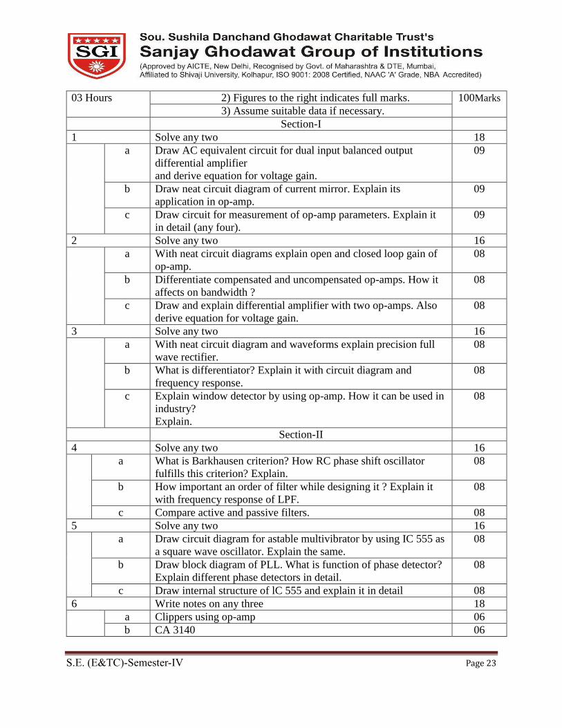
03 Hours 2) Figures to the right indicates full marks. 100Marks
3) Assume suitable data if necessary.
Section-I
1 Solve any two 18
a Draw AC equivalent circuit for dual input balanced output
differential amplifier
and derive equation for voltage gain.
09
b Draw neat circuit diagram of current mirror. Explain its
application in op-amp.
09
c Draw circuit for measurement of op-amp parameters. Explain it
in detail (any four).
09
2 Solve any two 16
a With neat circuit diagrams explain open and closed loop gain of
op-amp.
08
b Differentiate compensated and uncompensated op-amps. How it
affects on bandwidth ?
08
c Draw and explain differential amplifier with two op-amps. Also
derive equation for voltage gain.
08
3 Solve any two 16
a With neat circuit diagram and waveforms explain precision full
wave rectifier.
08
b What is differentiator? Explain it with circuit diagram and
frequency response.
08
c Explain window detector by using op-amp. How it can be used in
industry?
Explain.
08
Section-II
4 Solve any two 16
a What is Barkhausen criterion? How RC phase shift oscillator
fulfills this criterion? Explain.
08
b How important an order of filter while designing it ? Explain it
with frequency response of LPF.
08
c Compare active and passive filters. 08
5 Solve any two 16
a Draw circuit diagram for astable multivibrator by using IC 555 as
a square wave oscillator. Explain the same.
08
b Draw block diagram of PLL. What is function of phase detector?
Explain different phase detectors in detail.
08
c Draw internal structure of lC 555 and explain it in detail 08
6 Write notes on any three 18
a Clippers using op-amp 06
b CA 3140 06

S.E. (E&TC)-Semester-IV Page 24
c Log amplifier 06
d VCO. 06
Assignments
List of experiments/assignments to meet the requirements of the syllabus
Assignment No. 1
Assignment Title Introduction to OP-AMP CO208.1
Batch I
1) What is an integrated circuit? Explain its classification & types.
2) What is differential amplifier? What is the ideal value of its gain and
also explain its fundaments.
3) Explain the equivalent circuit of op-amp & also explain the op-amp
characteristics.
Batch II
1) Explain Ideal characteristics of op-amp.
2) Give the Comparative study of all four configurations of Differential
Amplifier.
3) Draw & explain the DC analysis of dual input balanced output type
Differential Amplifier.
4) Derive the expression for Differential gain (Ad) of dual input balanced
output type Differential Amplifier with respect to AC analysis.
Batch III
1) Draw neat circuit diagram of current mirror. Explain its application in
op-amp.
2) Give the block schematic of CA3130 or CA3140, explain its
operation and list its main features.
3) Define CMMR and explain the significance of a relatively large value
of CMRR.
Batch IV
1) What is an Op-amp? Explain block diagram Representation with neat
sketch.
2) Explain all parameters of Operational Amplifier.
3) Explain the following,
a) Input offset voltage b) Input offset current
c) Input bias current d) CMRR
e) Slew Rate f) PSSR
Assignment No. 2
Assignment Title Op-amp configurations & frequency response. CO208.2
Batch I 1) What is Open Loop & Closed Loop Configurations? Briefly explain
its types.
2) What is Frequency Response? Explain the Stability Specifications of
Frequency Response & Stability Criterion.
3) What is Frequency Compensation? Explain any one of Compensation
Technique.
Batch II 1) With typical frequency response of op-amp, explain the followings,
a) Gain Cross over frequency b) Gain Margin

S.E. (E&TC)-Semester-IV Page 25
c) Phase cross over frequency d) Phase Margin.
2) What is Frequency Response? Derive the Open Loop Voltage gain &
Phase angle equation as a function of frequency.
3) Define slew rate. An op-amp has slew rate of 1V/micro sec. Find the
largest sine wave output possible at a frequency of 1MHZ.
Batch III 1) Discuss methods of Frequency Compensation used in op-amp.
2) Explain difference between slew rate & transient response.
3) Differentiate compensated & uncompensated op-amps. How it affects
on bandwidth?
Batch IV 1) Draw and explain Differential Amplifier with two op-amps. Also
derive equation for voltage gain.
2) Explain the following:
a) Pole zero b) Dominant pole c) Feed forward Compensation
techniques.
3) What is slew rate? What are the causes? Derive the equation &
explain the improvement techniques for the same.
Assignment No. 3
Assignment Title Applications of Op-amp. CO3
Batch I 1) Explain V-I & I-V converter with design & specifications.
2) What id differentiator? Explain it with circuit diagram & frequency
response.
3) What is comparator? Explain characteristics.
4) What are precision rectifiers? Explain inverting & non-inverting half
wave rectifiers with equivalent circuit & waveforms.
Batch II 1) Explain the following:
a) Summing b) Scaling c) Averaging of an amplifier.
2) Write a brief note on Instrumentation Amplifier.
3) Explain subtract or difference amplifier.
Batch III 1) Explain Sample & Hold circuit? Why it is needed?
2) Explain the following:
a) Schmitt trigger b) Zero crossing detector
c) Peak detector d) Window detector.
3) Explain Precision Full wave rectifiers.
4) Draw & explain differential amplifier with two op-amp. Also derive
equation for voltage gain.
Batch VI 1) Explain temperature compensated Log & Antilog amplifier.
2) Explain Clipper & Clamper circuits?
3) Explain Log amplifier using diode & also using Transistor along with
basic fundamentals of Log amplifier.

S.E. (E&TC)-Semester-IV Page 26
Assignment No. 4
Assignment Title Active filters CO208.4
Batch I 1) Design 2nd order Butterworth low pass filter at cut off frequency 1khz
and feedback gain Af=3.
2) Compare passive filters and active filters.
3) Design 1st order Butterworth low pass filter for 1khz cut off frequency
and gain 2 in pass band.
Batch II 1) With neat waveform explain Band reject filter.
2) A certain two pole band pass filter response is required with a centre
frequency of 1.5khz & 3db bandwidth of 450hz, determine Q, Fl, Fh.
3) Explain All pass filter.
Batch III 1) Design a wide band pass filter having Fl=400hz, Fh=2khz and pass
band gain of 4. Find the value of Q of the filter.
2) Derive the equation for cut off frequency of 1st order Butterworth low
pass filter.
3) What is an Active filter explain its advantages & limitations.
Batch VI 1) Design band pass filter using sections of low/high pass filters with
pass band frequency of range=1khz to 3khz and gain in pass band =2.
2) Design 1st order Butterworth high pass filter for cut off frequency of
5khz, gain in pass band =5.
3) Explain what do you mean by Butterworth filter, Bessel filter,
chebyshev filter.
4) Draw and explain Sallen & key filter.
Assignment No. 5
Assignment Title Waveform Generators CO208.5
Batch I
1) What is Barkhausen criterion? How RC phase shift oscillator fulfills
this criterion? Explain.
2) Explain working of sine wave oscillator.
3) Draw circuit diagram for astable multivibrator by using IC 555 as
square wave oscillator and explain the same.
4) Design the phase shift oscillator using op-amp so that F0=200 hz.
Batch II
1) Design a square wave using IC 555 for given specifications:
Frequency of oscillations=2khz, duty cycle=60%, amplitude=5v.
2) Explain the principle of crystal oscillator.
3) Draw and explain square wave generation (astable multivibrator)
using op-amp.
4) Draw the internal structure of IC 555 and explain in detail.
Batch III
1) Draw pin diagram of IC 555 and explain each in detail.
2) Design astable multivibrator circuit with 50% duty cycle and 3khz
output frequency using IC 555.
S.E. (E&TC)-Semester-IV Page 27
3) Design an astable multivibrator circuit which will flash electric bulb
such that its ON time will be 4 seconds and OFF time will be 2 seconds.
4) Draw and derive the expression for the output frequency of RC phase
shift oscillator.
5) Draw and explain monostable multivibrator using IC 555.
Batch VI
1) Draw neat circuit diagram of weinbridge oscillator and derive
equation for frequency of oscillations.
2) Draw and explain colpitts oscillator.
3) Draw and explain sawtooth wave generator.
4) With neat wave form, explain triangular wave generation.
Assignment No. 6
Assignment Title Phase Locked Loop CO208.6
Batch I
1) Draw and explain transfer characteristics of PLL.
2) Draw the block diagram of PLL. Explain the function of phase
detector & also different phase detectors in detail.
Batch II 1) Write a note on frequency synthesizers.
2) Explain any one application of 565 PLL.
Batch III
1) Explain the working of PLL using appropriate lock diagram and
explain any one application of the same.
2) Write a short note on operating principle of VCO.
Batch VI
1) With reference to PLL, define capture range, lock range and pull in
time.
2) Explain note on IC 4046
Experiments
List of Experiments
Exp. No. 1 Study of Opamp Parameters.
Exp. No.2
Study of Inverting, Non-Inverting Amplifier and Voltage Follower
Configurations.
Exp. No. 3 Study of Summing, Scaling and Averaging Amplifiers.
Exp. No. 4 Study of Current to Voltage and Voltage to Current Converters.
Exp. No. 5 Study of Comparator , Schmitt Trigger & Zero crossing detector.
Exp. No. 6 Study of precision full wave & half wave rectifier
Exp. No. 7 Study of. Second-Order Butterworth Filter.
Exp. No. 8 Study of Sine, Square and Triangular Wave Generator.
S.E. (E&TC)-Semester-IV Page 28
Exp. No. 9 Study of astable , monostable multivibrator
Exp. No. 10 Study of wein bridge oscillator

S.E. (E&TC)-Semester-IV Page 29
Course Title – Data Structure
Course Data Structures Course Code ETC209
Prepared by Mrs.J.M.Waykule Date 7/11/2017
Prerequisites Programming Basics, Basic concepts of C, CPP and basic concepts theory of data
structures like array, records and pointers.
Course Outcomes
At the end of the course the students should be able to:
CO209.1 Apply3knowledge of Programming in the Field of Linear and Non Linear data
Structure.
CO209.2 Describe1 inserting, deleting, searching though arrays, records, pointers, linked list.
CO209.3 Classify3 linked list and different operations like inserting, deleting of nodes.
CO209.4 Define1 stack and queues and their representation.
CO209.5 Construct 4 Binary Tree and Advanced trees.
CO209.6 Illustrate4 different types of graphs and their application and representation.
CO209.7 Identify1 the concept of Hashing, collision and chaining.
Mapping of COs with POs
PSO’s POs
Cos
PO1 PO2 PO3 PO4 PO5 PO6 PO7 PO8 PO9 PO10 PO
11 PO12 PSO
CO209.1 1 1
CO209.2 2 3 3 1 2 1
CO209.3 3 1 1
CO209.4 3 3 2 1 1
CO209.5 1
CO209.6 1 2 2
CO209.7 3 1
Degree of compliance: 1: Low, 2: Medium 3: High
S.E. (E&TC)-Semester-IV Page 30
Course Contents:-
Chapter
No. Title
No. of
Hours
Section I
1 Introduction & Overview
Introduction to theory of data structures & its data types, Algorithms:
complexity, time space trade-off with example.
01
2 Arrays, Records & Pointers
Introduction, linear arrays, representation of linear array in memory,
traversing linear arrays, inserting & deleting,
Sorting: bubble sort, searching: linear search, binary search,
Multidimensional arrays, Pointers: pointer arrays, Records: Record
structures, representation of records in memory, parallel arrays, matrices,
space matrices.
06
3 Linked Lists
Introduction, linked lists & its representation, Traversing & searching a
linked list, memory allocation, Garbage collection, insertion & deletion of
nodes of linked list, header linked list, twoway lists, programming
problems.
06
4 Stacks & Queues
Introduction to stacks, stack as an Abstract Data type , representation
through Arrays & linked lists ,Applications of stacks , stacks & recursion,
Queue as an abstract data type representation, cicular, double ended,
priority, application of queues
06
Section
II
5 Trees
Binary Tree: introduction, types, definition, properties, representations,
operations, binary tree traversal reconstruction, counting number of binary
trees, applications. Advanced trees : AVL trees or height balanced trees,
representation operation, Threaded binary trees, Expression trees. Multiway
trees: trees ,multiway search trees, B+ trees, Heaps, construction of a Heap.
08
6 Graphs
Introduction, Graph theory terminology, sequential representation of
graphs: Adjacency Matrix, Path matrix, Warshall’s Algorithm, shortest
paths, linked representation. Operations, Traversing, Posets, Topological
sorting
06

S.E. (E&TC)-Semester-IV Page 31
7 Hashing
Hashing, Hash functions, collision, chaining 03
Reference Books:
Sr. No. Title of Book Author Publisher/Edition Topics
1 Data structure using C ISRD group Tata McGraw
Hill
1,2, 4,5.
2 Data structures Seymour
Lipschautz
Tata McGraw
Hill 3,6,7.
3
Data structure using C & C++ Langsam,
Rubenstein,
Tenenbaun
PHI
2,5,6
4 Data structure & algorithm
analysis in C
Mark Allen Weiss Pearson
Education (LPE) 2,4,5,7
Marking scheme
Examination
Scheme
Theory Term Work OE Total
Max. Marks 100 25 -- 125
Contact
Hours/ week
2 2 -- 4
Evaluation Scheme
UNIT 6 Questions to be set of 18 Marks
Each
Chapter
numbers Instructions
I Q.No.-1, Q.No.-2, Q.No.-3 1, 2, 3 Solve Any 2 out of each
question
II Q.No.-4, Q.No.-5, Q.No.-6 4,5,6 Solve Any 2 out of each
question
Scheme of Marks
Section Unit No. Title Marks
I 1. Introduction & Overview 12
I 2. Arrays, Records & Pointers 24
I 3. Linked Lists 16

S.E. (E&TC)-Semester-IV Page 32
I 4. Stacks and Queues 16
II 5. Trees 12
II 6. Graphs 8
II 7. Hashing 8
Course Unitization
Section
Unit Course
Outcomes No. of Questions in
No. Title CAT-I CAT-II CAT-III
I 1. Introduction &
Overview
CO209.1 02
2. Arrays, Records &
Pointers:
CO209.2 02
3. Linked Lists: CO209.3 02
II 4. Stacks & Queues CO209.4
03
5. Trees CO209.5 03
6. Graphs CO209.6
03
7. Hashing CO209.7 03
Unit wise Lesson Plan
Section I
Unit No 01 Unit Title Introduction & Overview:
Planned
Hrs.
01
Lesson schedule
Class No. Details to be covered
1 Explain the theory of data structures an its data types
2 Explanation of complexity and time space state of algorithms
Review Questions
Q1 What is Data Structure? Explain different data types. CO209.1

S.E. (E&TC)-Semester-IV Page 33
Q2 Briefly describe notions of algorithms and time space state of algorithms CO209.1
Unit No 02 Unit Title Arrays, Records & Pointers
Planned
Hrs.
06
Lesson schedule
Class
No.
Details to be covered
1 Arrays and types of array
2 Sorting with Different Sorting methods e.g. Bubble sort, Insertion sort, Selection sort
3 Linear Searching, binary Searching,
4 Multidimensional Array with its representation in memory
5 Pointers and advantage of pointer.
6 Records, Parallel arrays, matrices, sparse matrices
Review Questions
Q1 List the operations performed on Linear Data Structure. CO209.2
Q2 What is Linear Array? How Linear Arrays are represented in memory? CO209.2
Q3 Write algorithms for inserting and deleting element in Linear Array-
a. Inserting element in array at given location in array
b. Deleting element from given location in array Traversing the
Linear Array
CO209.2
Q4 What is Sorting? Explain Bubble Sort with algorithms. CO209.2
Q5 What is Searching? Explain Linear Search and Binary Search with
algorithms.
CO209.2
Q6 What is Multidimensional array? Explain Two-dimensional array and its
representation in memory.
CO209.2
Q7 What is Pointer Array? CO209.2
Q8 What is Record? Explain indexing items in Record. CO209.2
Q9 What is Matrices? Explain Sparse Matrices CO209.2
Unit No 03 Unit Title Linked Lists:
Planned
Hrs.
06
Lesson schedule
Class
No.
Details to be covered
1 Linked list with its representation in memory
2 Linked list with different basic operation performed on it.
3 Types of linked list
4 Insertion and deletion of nodes of linked list

S.E. (E&TC)-Semester-IV Page 34
5 Two ways lists i.e. circular linked list
6 Header linked list
Review Questions
Q1 What is linked list? Explain representation of linked list in memory? CO209.3
Q2 Explain traversing of linked list? Write algorithm for traversing and also write
procedure g of printing information present at each node & procedure for
finding number of element in the linked list?
CO209.3
Q3 Write an algorithm for finding out the location of node where item appears first
in the list in unsorted & sorted list
CO209.3
Q4 Explain garbage collection? Also explain overflow & underflow situations. CO209.3
Q5 Explain insertion of node into a linked list, write an algorithm to insert nodes –
1) At the beginning of list.
2) After a given node
3) Into sorted linked list
CO209.3
Q6 Explain deletion of node from linked list. Write an algorithm for deleting node
following a given node
CO209.3
Q7 Write a procedure for deleting node with a given item of information. CO209.3
Q8 Explain header linked list. Explain two way list & two way header list CO209.3
Q9 Write operations on two way lists? CO209.3
Unit No
04
Unit Title
Stacks & Queues:
Planned Hrs.
05
Lesson schedule
Class No. Details to be covered
1 Stack as an abstract data type with basic operation on Stacks
2 Representation of stacks through arrays and linked list
3 Queue as an abstract data type
4 Circular and double ended, priority queue
5 Applications of stacks and queues
Review Questions
Q1 What is stack? Explain Stack as an abstract data type. CO209.4
Q2 Explain representation of Stack through array. Write algorithm for PUSH and
POP operation.
CO209.4

S.E. (E&TC)-Semester-IV Page 35
Q3 Explain representation of Stack through linked list. Write algorithm for PUSH
and POP operation.
CO209.4
Q4
Write algorithms for a) Transforming Infix to postfix expression. b) Evaluation
of Postfix expression .c)Transforming Infix expression to Prefix expression)
Evaluation of Prefix expression
CO209.4
Q5 What is Queue? Explain Queue as an abstract data type. CO209.4
Q6 Explain representation of Queue through array. Write procedure for CO4
insertion and deletion of element operation.
CO209.4
Q7 Explain representation of Queue through linked list. Write procedure for CO4
insertion and deletion of element operation.
CO209.4
Q8 Explain Circular queue. CO209.4
Q9 Explain Double Ended Queues (DEQUES) CO209.4
Q10 Explain Priority Queues. CO209.4
Q11 List few applications of Stack and queue. CO209.4
Unit
No
5 Unit Title Trees Planned
Hrs.
08
Lesson Schedule
Class No. Details to be covered
1 Introduction to Binary Tree and its types.
2 Definition, properties and representations of Binary Tree.
3 Operations of binary tree, traversal and reconstruction of it.
4 Counting number of binary trees and applications.
5 Study of AVL trees or height balanced trees.
6 Representation and operation of Threaded binary trees
7 Study of multiway trees, multiway search trees.
8 Study of B+ trees, Heaps, construction of a Heap.
Review Questions
Q1 What is tree? List various types of trees & with neat diagram explain
any three types of trees
CO209.5
Q2 Reconstruct the following binary tree:Inorder: HDIJEKBALFMCNGO
Postorder: HIDJKEBLFMNOGCA
CO209.5
Q3 Explain insertion & deletion of node in binary tree. CO209.5
Q4 Explain insertion of node in AVL tree with different preposition. CO209.5

S.E. (E&TC)-Semester-IV Page 36
Q5 Explain construction of heap tree.Write algorithm for insertation into the
heap tree.
CO209.5
Q6 Write short note on: Multiway tree, Heap tree. CO209.5
Unit
No
6 Unit Title Graphs Planned Hrs. 06
Lesson schedule
Class
No.
Details to be covered
1 Introduction to Graph and graph theory terminology
2 Study of sequential representation of graphs
3 Study of Adjacency Matrix, Path matrix
4 Warshall’s Algorithm, shortest paths, linked representation
5 Study of Traversing and its Operations
6 Posets, Topological sorting
Review Questions
Q1 Write an algorithm for shortest path & explain. CO209.6
Q2 With proper diagram explain linked representation of graph CO209.6
Q3 Write an algorithm for inserting an edge in a graph CO209.6
Q4 Write a short note on Directed & Undirected graph. CO209.6
Q5 Explain Warshall’s Algorithm with suitable example CO209.6
Unit
No
7 Unit
Title
Hashing Planned
Hrs.
03
Lesson schedule
Class
No.
Details to be covered
1 Introduction to Hashing
2 Study of Hash functions
3 Study of collision, chaining
Review Questions
Q1 What is Hashing? CO209.7
Q2 Explain different hash functions CO209.7

S.E. (E&TC)-Semester-IV Page 37
Model Question Paper
Course Title : Data structures
Duration :- 3 Hours Total Marks 100
Instructions: All questions are compulsory.
Section-I
Marks
1 Attempt any two
A Define array and Explain with syntax and example initialization
and declaration of an array
8
B Explain with example and algorithm linear search Method 8
C Define Queue and explain its representation using array. 8
2 Attempt any two
A Explain with example and algorithm PUSH operation in a
Stack.
8
B Write a C code for insertion of an element in an array. 8
C What is Data Structure and Explain different types of data
Structure.
8
3 Write short note(any three)
a) POP OPeration
b) APPlication of stack and queue 8
c) Binary search 8
d) Multidimensional Array 8
Section-II
4 Attempt any two Marks
A Explain the Deletion of Node or element in a tree. 9
B Explain representation of Graph with example. 9
C Write an algorithm for inserting an edge in a graph 9
5 Attempt any two
A Explain open hashing and closed hashing method. 8
B b) Explain Warshall's Algorithm with example. 8

S.E. (E&TC)-Semester-IV Page 38
C c) A Binary Tree has 9 Nodes. The Preorder and inorder
sequence is as , follow :Inorder:EACKFHDBG
Preoder:FAEKCDHGB
Draw Binary Tree.
8
6 Write short note on any three
a) Heap 8
b) Breath First search (BFS) 8
c) Hash Function 8
d)Tree representation using Array and Link Iist 8
Assignments
List of assignments to meet the requirements of the syllabus
Assignment No. 1
Assignment Title Linear Array, Linear Searching, Linked List CO209.1
Batch I What is data structure? Explain its data types CO209.1
Batch II What is a linear array? Explain inserting and deleting of an
element in an linear array
CO209.2
Batch III Explain linear search and binary search with examples CO209.2
Batch IV Explain insertion and deletion of a node of a linked list CO209.3
Assignment No. 2
Assignment Title Stacks and Queues CO209.4
Batch I Explain Recursion in stack CO209.4
Batch II Explain Circular and double ended, priority queue CO209.4
Batch III Explain Insertion and deletion of nodes of linked list CO209.4
Batch IV Explain insertion and deletion in stack CO209.4

S.E. (E&TC)-Semester-IV Page 39
Assignment No. 3
Assignment Title Trees CO209.5
Batch I Explain deletion in m-way search tree with example
CO209.5
Batch II Explain deletion in m-way search tree with proper
example. CO209.5
Batch III
Reconstruct the following binary tree
Inorder: HDIJEKBALFMCNGO
Postorder: HIDJKEBLFMNOGCA
CO209.5
Batch IV Explain deletion in m-way search tree with proper
example.
CO209.5
Assignment No. 4
Assignment Title Graphs CO209.6
Batch I a) Explain Warshall's Algorithm with example.
b) Write an algorithm for inserting a node in a graph
CO209.6
Batch II Explain BFS and DFS algorithm
CO209.6
Batch III
For following graph shown below.
a) Find indeg (X) and outdeg (X)
b) Find all simple paths from Y to W.
c) Are there any source of sinks?
CO209.6
Batch IV a)Write and explain algorithm for topological sorting
b) Write an algorithm for inserting a edge in a graph.
CO209.6
Assignment No. 5
Assignment Title Hashing CO209.7
Batch I Explain the different collision resolution techniques.
Batch II Discuss briefly different hash functions.
Batch III What is hashing? Explain different hash f unctions.
Batch IV Explain how chaining is used in Collision resolution.
List of open ended assignments
Assignment No. 1
Assignment Title CO

S.E. (E&TC)-Semester-IV Page 40
Batch I Write an algorithm for breadth first search. Explain with
example CO209.3
Batch II Define AVL tree. Explain insertion in AVL tree with different
rotation CO209.7
Batch III Explain Threaded binary tree
CO209.6
Batch IV Explain Topological sorting CO209.4
List of experiments
List of experiments to meet the requirements of the syllabus
Experiment No. Experiment title CO
1. Program to Insert the Number in an Array CO209.2
2. Program to Delete the Number in an Array CO209.2
3. Program on Bubble Sort CO209.2
4. Program to Perform Linear search CO209.2
5. Program to Perform Binary search CO209.2
6. Program To Display 2D Array CO209.2
7. Program to Insert the Node in Link List CO209.3
8. Program to Delete the Node in Link List CO209.3
9. Program to Perform Push and Pop Operation on Stack CO209.4
10. Program to Perform Operation on Queue CO209.4
11. To Study Properties of Binary tree CO209.5
12. To Study Traversing operation of Tree CO209.5
13. To Study Traversing operation of Graph CO209.6
14. To study Hash Function CO209.7
List of additional experiments
Experiment
No.
Experiment Title CO
1. Study of traversing operation on queue CO209.6
2. Study of traversing operation on stack CO209.5
S.E. (E&TC)-Semester-IV Page 41
3. Use of Hash function in a project CO209.7
List of open ended experiments
Experiment No. Experiment Title CO
1. To calculate shortest path between two nodes using hash
functions
CO209.7
2. Study of queue traversal algorithm with push pop operations CO209.6
3. Study of Linear searching with sorting. CO209.3

S.E. (E&TC)-Semester-IV Page 42
Course Title – Electromagnetic Engineering
Course Electromagnetic Engineering Course Code ETC210
Prepared by Mrs.S.K.Apte Mr.P.B.Nikam Date 10/11/2017
Prerequisites This course requires the student to know about-
Basic concepts of Mathematics 1, Mathematics 2, Fundamentals of Electrical
Engineering & Physics.
Course Outcomes
At the end of the course the students should be able to:
CO210.1 Tell1fundamental lawsof Static Electromagnetic Fields.
CO210.2 Explain2various parameters related to Electromagnetic theory , Electrostatic
& Electromagnetic fields.
CO210.3 Solve3 examples based on dielectric material and boundary conditions in
Electrostatic & Electromagnetic fields.
CO210.4 Explain4 Maxwell’s equations and concepts of transmission lines.
CO210.5 Evaluate5 techniques for formulating and solving problems in Electrostatic &
Electromagnetic fields.
CO210.6 Develop6 problem solving skills related to transmission line and smith chart
Mapping of COs with POs
POs
/PSO's
Cos
PO1 PO2 PO3 PO4 PO5 PO6 PO7 PO8 PO9 PO10 PO
11 PO12 PSO1
CO210.1 3 1 2
CO210.2 3 1 2
CO210.3 3 2 1
CO210.4 3 3 1 1
CO210.5 2 3 1 1
CO210.6 2 3 2 1 1
Degree of compliance: 1: Low, 2: Medium 3: High

S.E. (E&TC)-Semester-IV Page 43
Course Contents
Chapter
No. Title
No. of
Hours
Section I
1 Co-ordinate systems: Vector Algebra, Co-ordinate systems, Curl,
Divergence & Gradient, Stoke’s Theorem, Poisson’s and Laplace
Equations, Coulomb’s law, line, Surface & Volume Charge distribution,
uniqueness theorem.
08
2 Electrostatic Fields: Electric Field Intensity, Electric Field due to infinite
line and surface charges, Electric Flux Density, Gauss law (differential
and integral form) and its applications, Divergence Theorem, Electric
Potential and gradient. Work done, Energy Density, Electric Dipole and
moment
09
3 Dielectrics & Boundary conditions: Polarisation in Dielectrics, Boundary
conditions for Dielectric and Dielectric, Conductor and Dielectric,
Conductor and free space. Method of Images for point and line charge.
09
Section II
4 Magnetostatic Fields: Biotsavart law, Magnetic Field Intensity due to
infinite and finite line. Ampere’s Circuital Law in integral and differential
form, Magnetic flux density, Magnetic boundary conditions, vector
magnetic potential, Magnetic Torque, moment and dipole.
08
5 Wave Propagation: Maxwell’s Equations in point form & Integral form
for various fields, Wave equations, wave propagation through different
medium, skin depth, Poynting theorem, Reflection of plane wave.
08
6 Transmission Lines: Transmission Line equations, Characteristic
equation of infinite Transmission Line, Uniform terminated
Transmission Line, Input impedance, Phase velocity and group velocity,
Short circuited and open circuited line, Reflection coefficient VSWR,
smith chart (Numerical expected) and applications.
08
Text Books:
1 Engineering Electromagnetics - William .H. Hayt and J A Buck – 7th Edition – 2011.
2 Principles of Electromagnetics - Matthew N O. Sadiku – 4th Edition, Oxford publication 2009.
3 Electromagnetic Field Theory and Transmission Lines – Gottapu Sasibhushanarao – Wiley
India 2013.
Reference Books:
1 Electromagnetic Field Theory- Rakhesh Singh Kshetrimayum – Cengage Publishing –
2012.

S.E. (E&TC)-Semester-IV Page 44
2 Electromagnetic with applications - J.D. Kraus. (MGH Publications)- 4th Edition.
3 Fundamentals of Engineering Elecromagnetics– Sunil Bhooshan – Oxford University
press. 2012.
4 Elements of Electromagnetic fields - SurinderP.Seth (DhanpatRai Publications)
Marking Scheme
Examination Scheme Theory Term Work OE Total
Max. Marks 100 25 -- 125
Contact Hours/ week 4 4 -- 8
Evaluation Scheme
UNIT 6 Questions to be set of 18 Marks
Each
Chapter
numbers Instructions
I Q.No.-1, Q.No.-2, Q.No.-3 1, 2, 3 Solve Any 2 out of each
question
II Q.No.-4, Q.No.-5, Q.No.-6 4,5,6 Solve Any 2 out of each
question
Course Unitization
Secti
on
Unit Course
Outcome
s
No. of Questions in
No. Title CAT-I CAT-II CAT-III
I 1 Vector Analysis CO210.1 3
2 Electric Flux & Potential CO210.2 3
3 Dielectrics & Boundary
conditions:
CO210.3 3
II 4 Steady magnetic fields CO210.4 3
5 Electromagnetic waves CO210.5 3
6 Transmission Lines CO210.6 3

S.E. (E&TC)-Semester-IV Page 45
Unit wise Lesson Plan
Section I
Unit
No
01 Unit Title Coordinate systems Planned Hrs. 08
Lesson schedule
Class
No.
Details to be covered
1 Vector Algebra
2 Co-ordinate systems
3 line, Surface & Volume Integral
4 Divergence and Gradient
5 Curl
6 Electric Charge, Coulomb’s law
7 Charge distribution, Electric Field Intensity
8 Field due to distributed charges
Review Questions
Q1 Summarize difference between field and circuit theory with examples? CO210.1
Q2 Explain Line, Surface and Volume integral? CO210.1
Q3 State and explain Gradient, Divergence and Curl of a vector? CO210.1
Q4 Write Coulomb’s law and explain concept of Electric field intensity? CO210.1,
CO210.2
Q5 Numerical on point conversion in coordinate systems, finding
Gradient, Divergence and curl, Coulomb’s law and Distributed charge
system are expected.
CO210.1
Q6 Summarize difference between field and circuit theory with examples? CO210.2
Q7 Explain Line, Surface and Volume integral? CO210.1
Unit
No
02 Unit Title Electrostatic Field
Planned Hrs. 09
Lesson schedule
Class
No.
Details to be covered
1 Flux & Flux density
S.E. (E&TC)-Semester-IV Page 46
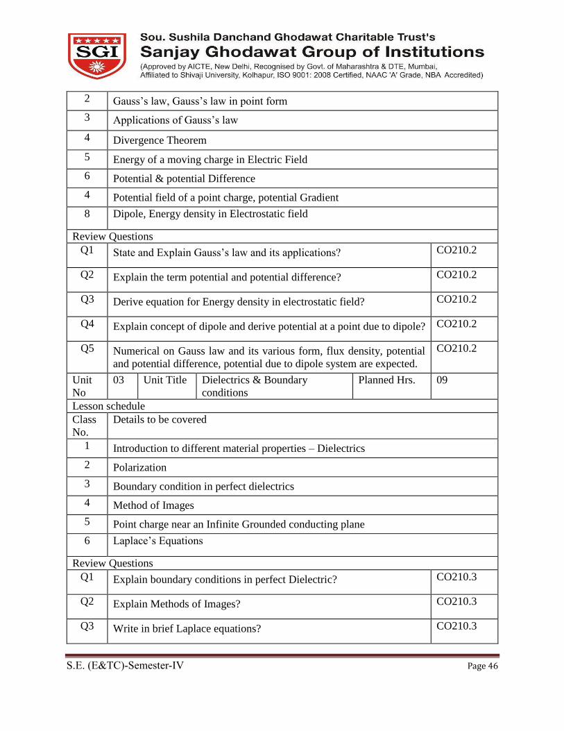
2 Gauss’s law, Gauss’s law in point form
3 Applications of Gauss’s law
4 Divergence Theorem
5 Energy of a moving charge in Electric Field
6 Potential & potential Difference
4 Potential field of a point charge, potential Gradient
8 Dipole, Energy density in Electrostatic field
Review Questions
Q1 State and Explain Gauss’s law and its applications? CO210.2
Q2 Explain the term potential and potential difference? CO210.2
Q3 Derive equation for Energy density in electrostatic field? CO210.2
Q4 Explain concept of dipole and derive potential at a point due to dipole? CO210.2
Q5 Numerical on Gauss law and its various form, flux density, potential
and potential difference, potential due to dipole system are expected.
CO210.2
Unit
No
03 Unit Title Dielectrics & Boundary
conditions
Planned Hrs. 09
Lesson schedule
Class
No.
Details to be covered
1 Introduction to different material properties – Dielectrics
2 Polarization
3 Boundary condition in perfect dielectrics
4 Method of Images
5 Point charge near an Infinite Grounded conducting plane
6 Laplace’s Equations
Review Questions
Q1 Explain boundary conditions in perfect Dielectric? CO210.3
Q2 Explain Methods of Images? CO210.3
Q3 Write in brief Laplace equations? CO210.3

S.E. (E&TC)-Semester-IV Page 47
Q4 Numerical on point charge near conducting plane and boundary
conditions are expected.
CO210.3
Unit
No
04 Unit Title Magnetic Fields Planned Hrs. 08
Lesson schedule
Class
No.
Details to be covered
1
Current and current Density, Biot-savarts law
2 Strokes theorem, Ampere’s law
3 Magnetic flux and Flux density
4 Vector magnetic potential
5 Derivation of steady magnetic fields law
Review Questions
Q1 State and Explain in detail Biot-savarts law? CO210.4
Q2 State and Explain Strokes theorem? CO210.4
Q3 Comment on vector magnetic potential? CO210.4
Q4 Derive steady magnetic field laws? CO210.4
Q5 Numerical on magnetic field laws are expected. CO210.4
Unit
No
5. Unit Title Electromagnetic Waves Planned Hrs. 08
Lesson schedule
Class
No.
Details to be covered
1. Maxwell’s equation in different forms
2. Retarded potential
3. Wave equation in free space
S.E. (E&TC)-Semester-IV Page 48
4. Wave propagation in different medium
5. Skin depth and poynting vector
Review Questions
Q1 State and Explain Maxwell’s equation for steady and time varying
field?
CO210.5
Q2 Explain wave propagation in different medium? CO210.5
Q3 Derive wave equation? CO210.5
Q4 What do you mean by Poynting vector? Define SWR? CO210.5
Q5 Numerical on wave propagation, skin depth, SWR and on Maxwell’s
equation are expected.
CO210.5
Unit
No
6 Unit Title Transmission Lines Planned
Hrs.
08
Lesson schedule
Class
No.
Details to be covered
1 Field Theory and circuit theory comparison
2 Transmission line equation
3 Different Transmission line parameters
4 Input Impedance
5 Terminated uniform transmission line
6 VSWR
Review Questions
Q1 Write difference between Field and Circuit theory? CO210.6
Q2 Define VSWR and derive transmission line equation? CO210.6
Q3 Explain Smith chart and its applications? CO210.6
Q4 Numerical on transmission line equation, smith chart, input impedance
are expected.
CO210.6
Model Question Paper
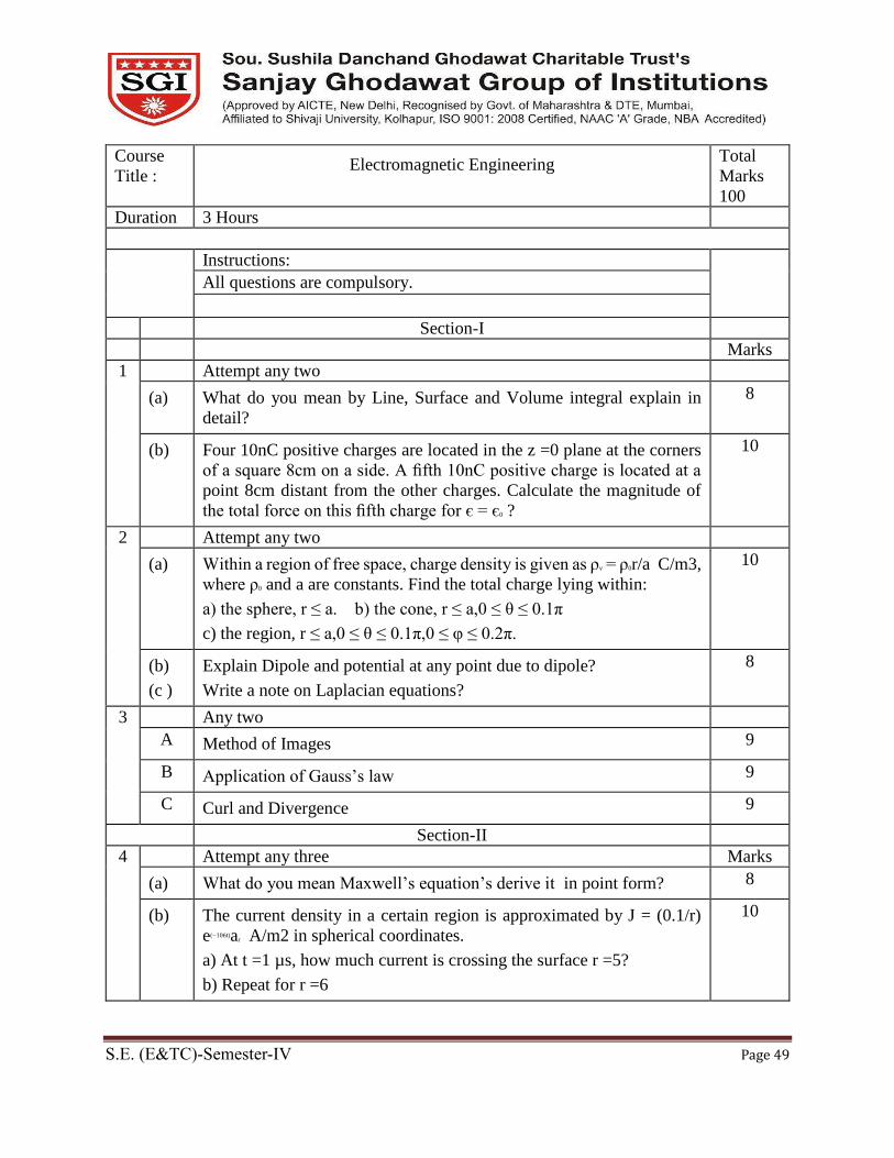
S.E. (E&TC)-Semester-IV Page 49
Course
Title : Electromagnetic Engineering
Total
Marks
100
Duration 3 Hours
Instructions:
All questions are compulsory.
Section-I
Marks
1 Attempt any two
(a) What do you mean by Line, Surface and Volume integral explain in
detail?
8
(b) Four 10nC positive charges are located in the z =0 plane at the corners
of a square 8cm on a side. A fifth 10nC positive charge is located at a
point 8cm distant from the other charges. Calculate the magnitude of
the total force on this fifth charge for є = є0 ?
10
2 Attempt any two
(a) Within a region of free space, charge density is given as ρv = ρ0r/a C/m3,
where ρ0 and a are constants. Find the total charge lying within:
a) the sphere, r ≤ a. b) the cone, r ≤ a,0 ≤ θ ≤ 0.1π
c) the region, r ≤ a,0 ≤ θ ≤ 0.1π,0 ≤ φ ≤ 0.2π.
10
(b)
(c )
Explain Dipole and potential at any point due to dipole?
Write a note on Laplacian equations?
8
3 Any two
A Method of Images 9
B Application of Gauss’s law 9
C Curl and Divergence 9
Section-II
4 Attempt any three Marks
(a) What do you mean Maxwell’s equation’s derive it in point form? 8
(b) The current density in a certain region is approximated by J = (0.1/r)
e(−106t)ar A/m2 in spherical coordinates.
a) At t =1 µs, how much current is crossing the surface r =5?
b) Repeat for r =6
10

S.E. (E&TC)-Semester-IV Page 50
c) Use the continuity equation to find ρv(r, t), under the assumption that
ρv → 0
as t →∞.
5 Attempt any two
(a) Find H in Cartesian components at P (2, 3, 4) if there is a
current filament on the z axis carrying
8mA in the az direction?
b. Repeat if the filament is located at x = −1, y =2.
c. Find H if both filaments are present.
10
(b) Write difference between circuit and field theory? Comment on Input
impedance.
5
(c) Derive any two steady magnetic field laws? 5
6 Write short note on any three
A Skin depth. 9
B Smith chart and its applications 9
C Stoke’s theorem
9

S.E. (E&TC)-Semester-IV Page 51
Course Title – Analog Communication Systems
Course Analog Communication Systems Course Code ETC211
Prepared by Mr. A. K. Rathod and Ms.K.M.Akkole Date 02/11/2017
Prerequisites Basic knowledge of Mathematics, Electrical Signals, electronic components , Analog and
digital signals etc.
Course Outcomes
Upon successful completion of this course, the student will be able to:
CO211.1 Demonstrate2 the knowledge of fundamental concepts and various components of analog
communication systems.
CO211.2 Identify2 and describe various analog modulation schemes.
CO211.3 Determine1 the performance of analog communications systems in the presence of noise.
CO211.4 Compare1 the merits and demerits of various analog communication systems.
CO211.5 Differentiate3 between various pulse modulation techniques.
Mapping of Cos with Pos
POs/
PSOs
COs
PO1 PO2 PO3 PO4 PO5 PO6 PO7 PO8 PO9 PO10 PO11 PO12 PSO1
CO211.1 3
CO211.2 2 3 2 1
CO211.3 2 3 1 1 2
CO211.4 2
CO211.5 1
Course Contents
Unit No. Title No. of
Hours
Section I
I
Amplitude Modulation:
Elements of electronic communication systems, Need for modulation,
channel, frequency spectrum, time and frequency domain signals, 09

S.E. (E&TC)-Semester-IV Page 52
Amplitude Modulation principles, AM envelope, frequency spectrum
& BW, phase representation of AM wave, Modulation index, %
modulation, AM modulating circuits: Low level AM modulation,
medium power AM modulation, AM transmitters: Block of low level
DSBFC, High level DSBFC, Trapezoidal patterns Evolution and
descriptions of SSB, Suppression of carrier using balanced modulator,
Suppression of unwanted sideband, Methods: Filter system, phase shift
& third method Vestigial sideband(VSB).
II
Angle Modulation:
Instantaneous frequency, Concept of angle modulation, frequency
spectrum, Narrow band & Wide Band FM, Modulation Index,
Bandwidth, Phase modulation, Bessel’s Function and its mathematical
Analysis, Generation of FM (Direct and Indirect Method), Comparison
of FM and PM.
08
III
AM Receiver:
Simplified block diagram of AM receiver, receiver parameters:
Sensitivity, Selectivity, BW, dynamic range, Tracking, fidelity, Types
of AM receiver: TRF and super heterodyne (block diagram), AM
detection types: using diode, practical diode detector, distortion in
diode detector. Negative peak clipping & diagonal clipping,
Demodulation of SSB using: product demodulator & diode balanced
modulator, Automatic Gain Control (AGC).
07
Section II
IV
FM Receiver:
Double conversion FM receivers, block diagram, FM demodulator,
tuned circuit frequency discriminators, slope detectors, Fosters Seeley
discriminator, ratio detectors, PLL-FM demodulators, FM noise
suppression.
07
V
Noise:
Sources of noise, Types of noise White noise, shot noise, thermal noise,
partition noise, low frequency or flicker noise, burst noise, avalanche
noise, signal to noise ratio, SNR of tandem connection. Noise Figure,
Noise Temperature, FRISS formula for noise figure, Noise bandwidth.
08
VI
Pulse Modulation :
Introduction, Sampling theorem: occurrence of aliasing error,
Mathematical proof of sampling theorem., PAM: Channel BW for
PAM, Natural Sampling, Flat-top Sampling, PAM & TDM, Signal
Recovery,; PWM: Uses of PWM, generation of Analog W/F using
PWM, PPM: Generation of PAM, Generation of PWM, Generation of
PPM; PCM Basics, PCM Transmitter and Receiver, Quantization.
09
Text Books:
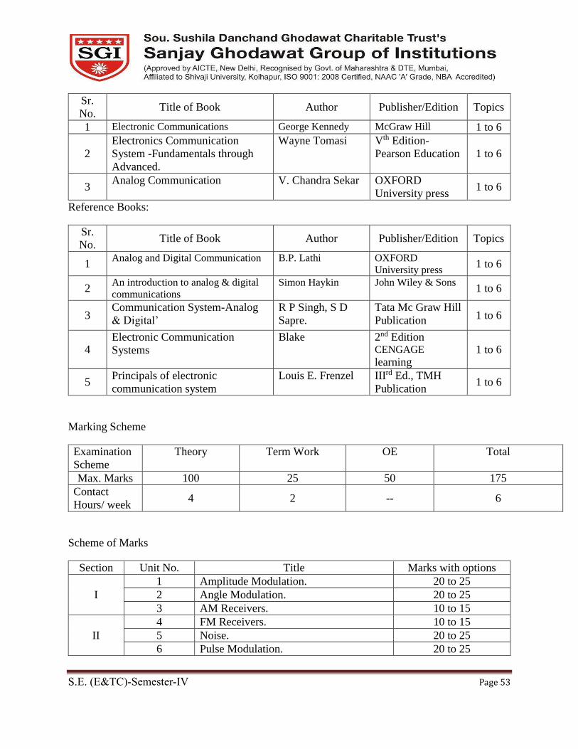
S.E. (E&TC)-Semester-IV Page 53
Sr.
No. Title of Book Author Publisher/Edition Topics
1 Electronic Communications George Kennedy McGraw Hill 1 to 6
2
Electronics Communication
System -Fundamentals through
Advanced.
Wayne Tomasi Vth Edition-
Pearson Education 1 to 6
3 Analog Communication V. Chandra Sekar OXFORD
University press 1 to 6
Reference Books:
Sr.
No. Title of Book Author Publisher/Edition Topics
1 Analog and Digital Communication B.P. Lathi OXFORD
University press 1 to 6
2 An introduction to analog & digital
communications Simon Haykin John Wiley & Sons
1 to 6
3 Communication System-Analog
& Digital’
R P Singh, S D
Sapre.
Tata Mc Graw Hill
Publication 1 to 6
4 Electronic Communication
Systems
Blake 2nd Edition CENGAGE learning
1 to 6
5 Principals of electronic
communication system
Louis E. Frenzel IIIrd Ed., TMH
Publication 1 to 6
Marking Scheme
Examination
Scheme
Theory Term Work OE Total
Max. Marks 100 25 50 175
Contact
Hours/ week 4 2 -- 6
Scheme of Marks
Section Unit No. Title Marks with options
I
1 Amplitude Modulation. 20 to 25
2 Angle Modulation. 20 to 25
3 AM Receivers. 10 to 15
II
4 FM Receivers. 10 to 15
5 Noise. 20 to 25
6 Pulse Modulation. 20 to 25

S.E. (E&TC)-Semester-IV Page 54
Course Unitization
Section
Unit Course
Outcomes
No. of Questions in
No. Title CAT-I CAT-II
I 1 Amplitude Modulation. CO211.1 2
2 Angle Modulation. CO211.1,
CO211.2
2
3 AM Receivers. CO211.1,
CO211.2
2
II 4 FM Receivers. CO211.2,
CO211.4
2
5 Noise. CO211.3
,CO211.4
2
6 Pulse Modulation. CO211.5 2
Unit wise Lesson Plan
Section I
Unit No I Unit Title Amplitude Modulation Planne
d Hrs. 09
Lesson schedule
Class
No. Details to be covered
1 Introduction to elements of electronic communication systems and its types.
Modulation, Need of Modulation
2 Amplitude Modulation, AM envelope, frequency spectrum & bandwidth requirement.
3 Phase representation of AM wave, Modulation index, % modulation.
4 Low level AM modulation, Medium Power AM modulation.
5 DSBFC Technique, High level Technique.
6 Trapezoidal patterns, Numerical on AM modulation.
7 DSBSC, SSB Techniques, Advantages of DSBSC & SSB techniques over conventional
AM modulation.
8 Balanced Modulator, filter method
9 Phase Shift method, Third method, VSB Technique.
Review Questions
Q1 Define modulation. Explain need of modulation. CO211.1
Q2 Explain the Third method for SSB technique. CO211.1
Q3 Explain the high level modulation technique in AM modulation. CO211.1
Q4 Explain and derive the expression of frequency spectrum of the AM wave. CO211.1
Q5 Describe the operation of a filter type SSB transmitter. CO211.1
Unit No II Unit Title Angle modulation Planne
d Hrs. 08
S.E. (E&TC)-Semester-IV Page 55
Lesson schedule
Class
No. Details to be covered
1 Concept of angle modulation, its purpose and advantages over FM.
2 Modulation index, Bandwidth requirement of FM waves.
3 Bessel’s function.
4 Phase modulation.
5 Mathematical Analysis of FM and PM wave.
6 Generation techniques of PM wave.
7 Generation techniques of FM wave.
8 Pre-emphasis and De-emphasis.
9 Comparison of AM, FM and phase modulation technique.
Review Questions
Q6 Define following terms:- Instantaneous frequency, Instantaneous phase. CO211.1
Q7 Derive mathematical expression for FM wave. CO211.2
Q8 Write a short note on angle modulation using Varactor diode. CO211.2
Q9 What is Pre-emphasis and De-emphasis? CO211.2
Q10 Describe significance of Bessel function and Bessel Table. CO211.2
Unit No III Unit Title AM Receiver Planned
Hrs. 07
Lesson schedule
Class
No. Details to be covered
1 Various AM receiver characteristics.
2 Types of AM receivers: TRF
3 Super heterodyne receiver.
4 AM detection types: Using diode, practical diode detector.
5 Distortion in diode detector: Negative peak clipping & Diagonal clipping.
6 Demodulation techniques for SSB techniques:- Product demodulator.
7 Diode Balanced modulator, AGC (automatic gain control).
Review Questions
Q11 Explain Sensitivity, Selectivity and fidelity characteristics of AM receiver. CO211.2
Q12 Give drawbacks of TRF receiver. Explain Superheterodyne receiver in
detail.
CO211.2
Q13 Explain working of practical diode detector in AM receiver and its
drawbacks.
CO211.2
Q14 Explain working of balanced diode modulator of SSB demodulation
technique in detail.
CO211.2
Q15 What is the purpose of AGC in AM receiver? How does it work? Explain in
detail.
CO211.2

S.E. (E&TC)-Semester-IV Page 56
Section II
Unit No IV Unit Title FM Receiver Planned
Hrs. 07
Lesson schedule
Class
No. Details to be covered
1 Double conversion FM receiver.
2 FM demodulator: Tuned Circuit Frequency Discriminators.
3 Slope Detectors.
4 Foster’s Seeley Discriminator.
5 Ratio Detectors.
6 PLL-FM Demodulators.
7 FM Noise Suppression.
Review Questions
Q1 Explain Double conversion FM receiver with the help of block diagram. CO211.4
Q2 What are different types of FM receiver? CO211.4
Q3 Explain working of Foster’s Seeley Discriminator. CO211.4
Q4 Draw and explain working of PLL-FM Demodulators. CO211.4
Q5 Explain FM Noise Suppression techniques using limiter. CO211.4
Unit No V Unit Title Noise Planned
Hrs. 08
Lesson schedule
Class
No. Details to be covered
1 Introduction to Noise.
2 Types of Noise: White Noise, Shot Noise, Thermal Noise.
3 Partition Noise, Low frequency/Flicker noise, Burst Noise, Avalanche Noise.
4 Signal to Noise ratio, Noise figure.
5 Noise temperature.
6 FRISS formula for noise figure.
7 Noise Bandwidth.
8 Numerical on SNR calculation.
Review Questions
Q6 Define Noise. Explain Thermal Noise. CO211.3,
CO211.4
Q7 Derive the expression for SNR. CO211.3,
CO211.4
Q8 What is Noise Figure? Explain Shot Noise. CO211.3,
CO211.4
Q9 What is FRISS formula explains? CO211.3,
CO211.4

S.E. (E&TC)-Semester-IV Page 57
Q10 What is the relation of BW and noise? Explain partition noise. CO211.3,
CO211.4
Unit No VI Unit Title Pulse Modulation Planned
Hrs. 09
Lesson schedule
1 Introduction to PM modulation, Sampling theorem.
2 Mathematical Proof of sampling theorem.
3 Types of sampling: Natural and Flat-top Sampling.
4 Generation of PM wave.
5 Generation of PAM wave.
6 Generation of PPM wave.
7 Generation of PWM wave.
8 PCM Transmitter.
9 Quantization method.
Review Questions
Q11 What is meant by Sampling? Explain its types. CO211.5
Q12 Explain PAM modulation circuit in detail. CO211.5
Q13 Explain PPM modulation circuit in detail. CO211.5
Q14 Explain PWM modulation circuit in detail. CO211.5
Q15 Explain Quantization and its purpose. CO211.5
Model Question Paper
Course
Title : Analog Communication Systems Max.
Marks 100 Duration 3 hrs
Instructions: i) Figures to the right indicate full marks
ii) All questions are compulsory.
iii) Assume necessary data wherever necessary.
Section-I
Marks
Q1 Attempt any two questions of the following.
A Prove that Pt= Pc (1+m2/2). Describe the significance of above formula. 8
B Explain the need and principal of Pre-emphasis and de-emphasis in FM. 8
C With neat block diagram Explain superhyterodyne AM receiver 8
S.E. (E&TC)-Semester-IV Page 58
Q2 Attempt any two questions of the following.
A With the help of block diagram explain the SSB suppression using
balanced modulator. 8
B Define the following terms:
1. Frequency deviation
2. Phase deviation
3. Deviation sensitivity for FM
4. Deviation sensitivity for PM
8
C For an DSBFC AM wave with a peal unmodulated carrier voltage
Vc=10V, load resistance RL=10Ω and modulation co-efficient m=1,
determine
i.Power of the carrier signal.
ii.Power of the lower and upper side bands.
8
Q3 Write Short note on following (any three)
A Significance of Bessel function in FM. 6
B Automatic Gain Control 6
C Receiver Paremeters 6
D Low level AM transmitter 6
Section-II
Q4 Attempt any two questions of the following. Marks
A Explain double conversion FM receiver. 8
B Draw and Explain PPM demodulator Circuit. 8
C Derive the expression for SNR. 8
Q5 Attempt any two questions of the following.
A Explain Foster-Seeley discriminator for FM. 8
B Mathematical Proof of sampling theorem. 8
C Explain PCM Transmitter and Receiver. 8
Q6 Write Short note on following (any three)
A Crosstalk in PAM 6
B FM Noise Suppression 6
C Pulse width Modulation 6
D Internal Noise sources. 6
List of experiments/tutorials to meet the requirements of the syllabus
1. Practical Implementation of Amplitude Modulation and Demodulation.
2. Calculation of modulation index by graphical method of DSBFC signal & measurement of
power of AM wave for different modulating signal.
3. SSB modulation using any method (filter method, Phase shift method) and its detection.
4. Envelope detector- Practical diode detector.
5. Performance and analysis of AM system using trapezoidal method
6. Performance and analysis of frequency modulator system and also find the modulation

S.E. (E&TC)-Semester-IV Page 59
index
7. Experiment on Sampling and reconstruction and also observe aliasing effect by varying
sampling frequency.
8. Practical implementation of PAM system
9. Practical implementation of PPM system
10. Practical implementation of PWM system
11. Practical implementation of PAM-TDM systems.
12. Experiment on Pre-emphasis and De-emphasis.
13. Visit to AIR
At least one experiment based on simulation software.
(Question Paper should include 70% theory and 30% numerical.)
Assignment No. 1
Assignment
Title Amplitude Modulation CO211.1
Q1 Explain elements of Basic Electronic Communication systems.
Q2 Define modulation and List its types.
Q3 Explain the need of modulation. Define modulation index and % modulation.
Q4 Prove that Pt= Pc (1+m2/2). Describe the significance of above formula.
Q5 For an DSBFC Am wave with a peak modulated carrier voltage Vc=10V load
resistance RL=10Ω and modulation coefficient m=1,determine
i) Power of the carrier signal ii) Power of upper and lower sidebands.
Q6 Calculate modulation index from trapezoidal display.
Q7 Explain any one type of SSB generation technique.
Q8 Explain in detail Vestigial Sideband technique (VSB).
Assignment No. 2
Assignment
Title Angle Modulation
CO211.1,
CO211.2
Q1 Derive mathematical expression for FM wave.
Q2 Define following terms: i) Instantaneous Phase ii) Instantaneous Phase deviation
iii) Instantaneous frequency iv) Instantaneous frequency deviation.
Q3 Define modulation index,% modulation index in FM. Effect of modulation index
on bandwidth of FM.
Q4 Write a short note on angle modulation using Varactor diode.
Q5 Describe the significance of Bessel function and Bessel table.
Q6 Explain FM generation using Indirect Method.
Q7 Compare AM and FM.
Assignment No. 3

S.E. (E&TC)-Semester-IV Page 60
Assignment
Title AM Receiver
CO211.1,
CO211.2
Q1 Define AM demodulation. Draw block diagram of AM receiver. Explain operation
of each block.
Q2 Explain why local oscillator is used in AM receiver.
Q3 Define and describe following receiver parameters:
i) Sensitivity ii) Selectivity iii) Fidelity iv) Tracking v) Dynamic range.
Q4 Explain with block diagram Superheterodyne receiver.
Q5 Explain with block diagram TRF receiver.
Q6 Write a note on Automatic Gain Control.
Q7 With respect to AM diode detector describe:
i) Diagonal clipping and its causes.
ii) Negative peak clipping with neat waveforms.
Assignment No. 4
Assignment
Title FM Receiver
CO211.2,
CO211.4
Q1 Draw and explain block diagram of double conversion FM receiver.
Q2 Comment on FM noise suppression. Draw and explain single stage tuner limiter
circuit.
Q3 What is meant by front end of the receiver? What are the primary functions of the
front end of the receiver, explain it with block diagram of the receiver.
Q4 Draw the schematic diagram of simple slope detector and describe its operation.
Draw voltage Vs frequency curve.
Q5 Describe the process of FM demodulation. Explain with block diagram PLL-FM
demodulator.
Q6 Explain with schematic diagram and vector diagram Foster – Seeley discriminator
Assignment No. 5
Assignment
Title Noise
CO211.3,
CO211.4
Q1 Define Noise. List various types of noise.
Q2 Define Signal to Noise ratio. Explain Thermal noise.
Q3 Give FRISS formula for noise figure. Explain Noise temperature.
Q4 Short note on White noise, Avalanche Noise, Partition noise.
Q5 Derive the expression for SNR.
Assignment No. 6
Assignment
Title Pulse Modulation CO211.5

S.E. (E&TC)-Semester-IV Page 61
Q1 Explain PAM modulation, demodulation and sampling.
Q2 State and explain sampling theorem, aliasing effect with neat waveform.
Q3 Discuss types of sampling.
Q4 Explain PCM Transmitter and Receiver.
Q5 Draw and explain PWM modulator and demodulator circuits.
Q6 Draw and explain PPM modulator and demodulator circuits.
Q7 Explain TDM in detail and explain crosstalk in detail.

S.E. (E&TC)-Semester-IV Page 62
Course Title – Circuit Simulation
Course Circuit Simulation Course Code ETC212
Prepared by MR.MATTADA M.P. Date 10/11/2017
Prerequisites Basics of Analog and Digital circuit analysis and synthesis, fundamental
knowledge and working principles of analog and digital circuits.
Course Outcomes
At the end of the course the students should be able to:
CO212.1 Analyse4, synthesize and simulate a given digital or analog circuit using
OrCAD, OsCAD, MultiSim and Proteus.
CO212.2 Analyse4 a given electronic circuit using simulation software for different
types of analysis (AC/DC).
CO212.3 Develop6 the basics of PCB and Design of simple PCB as per required
specification.
Mapping of COs with POs/PSOs
POs/PSOs
COs
PO1 PO2 PO3 PO4 PO5 PO6 PO7 PO8 PO9 PO10 PO11 PO12 PSO1
CO212.1 3 3 3 3 1 2 1
CO212.2 3 3 3 3 1 2 2 2
CO212.3 3 3 3 3 1 3 3 3 3
1: Low 2: Medium 3: High

S.E. (E&TC)-Semester-IV Page 63
Course Contents
Unit No. Circuit Simulation No. of
Hours
Section I
1. Schematic Design:
Introduction, Description of P-Spice, Types of analysis, Description of
simulation software tools (like OrCAD / Proteus), Schematic
Description, Introduction, Input files, element values, Nodes, circuit
elements, sources, output variables, format of circuit and output files,
drawing the schematic, Design rule Check (DRC ), Net list details.
(04)
2. Simulation:
Types of Analysis: Bias point, Time domain, AC Sweep, DC Sweep,
Parametric, Monte Carlo, Noise analysis. Cover vertical devices also
using MultiSim, OrCAD, Proteus, OsCAD.
(04)
3. PCB Design:
IC packages, Types of Connectors, Net list for layout, Types of PCB’s,
Description of layout design tool, foot- print creation, Setting board
parameter ( board template, layer strategies), Component placement
considerations, Routing strategies, Design Rule check, back annotation,
post processing reports. Software: Express PCB.
(04)
Reference Books:
Sr. No. Title of Book Author Publisher/Edition Topics
1. Introduction to P-spice using OrCAD
for circuits and Electronics.
M. H. Rashid Pearson Education U1,U2
2. Electronic Circuits-Fundamentals and
Applications.
Mike Tooley 3rd Edition – Vikas U1,U2

S.E. (E&TC)-Semester-IV Page 64
Publication
(Routledge)
3. Printed Circuit Boards-Design &
Technology.
W.C.
Bosshart
Tata McGraw-Hill
Publication.
U3
4. User manuals of PROTEUS, OrCAD,
MultiSim. - - -
5. User manuals of OSCAD, Express PCB
from IIT, Pawai. - - -
Examination
Scheme
Theory Term Work POE Total
Max. Marks -- 25 -- 25
Contact
Hours/ week --
Practical: 2
hrs/week
-- 2
Unit wise Lesson Plan
Unit
No
1 Unit Title Schematic Design Planned
Hrs.
04
Lesson schedule
Class
No.
Details to be covered
1 Introduction, Description of P-Spice, types of analysis.
2 Description of simulation software tools (like OrCAD / Proteus).

S.E. (E&TC)-Semester-IV Page 65
3 Schematic Description: Introduction, Input files, element values, Nodes, circuit
elements, sources, output variables, format of circuit and output files, drawing the
schematic.
4 Design rule Check (DRC), Net list details.
Unit
No
2 Unit Title Simulation Planned
Hrs.
04
Lesson schedule
Class
No.
Details to be covered
1 Types of Analysis: Bias point, time domain.
2 AC Sweep, DC Sweep, Parametric.
3 Monte Carlo analysis, Noise analysis.
4 Cover vertical devices also using MultiSim, OrCAD, Proteus, and OsCAD.
Unit
No
3 Unit Title PCB Design Planned
Hrs.
04
Lesson schedule
Class
No.
Details to be covered
1 IC packages, Types of Connectors, Net list for layout.
2 Types of PCB’s, Description of layout design tool, foot- print creation.
3 Setting board parameter (board template, layer strategies), Component placement
considerations.
4 Routing strategies, Design Rule check, back annotation, post processing reports,
Software: Express PCB.

S.E. (E&TC)-Semester-IV Page 66
List of experiments
Experiment
No.
Experiment title
1. Introduction P-Spice tool.
2. Study of Inverting, Non-Inverting & voltage follower Op-amp.
3. Study of Differentiator & Integrator using Op-amp.
4. Study of Summing, Scaling and Averaging Amplifier.
5. To study Transient analysis & Rectifiers (HALF, FULL, BRIDGE WAVE
Rectifiers).
6. Transfer Function Analysis of BJT amplifiers.
7. Study of Proteus tool.
8. Realization of Logic Gates.
9. Realization of Counter using J-K flip-flops.
10. Experiment for BCD to Seven segment display using push buttons.
11. To study BCD counter using IC 74LS90.
12. Finding node Voltages and Current of a circuit.
13 Finding Thevenin’s Equivalent values.
14. Pulse Response & Step Response of an RLC circuit.
15. Experiment for LDR.
16. Experiment for Realization of Clipper and Clamper (Positive, Negative
Clipper/ Clamper).
List of Additional Experiments
1. Simple experiment of PCB designing.
S.E. (E&TC)-Semester-IV Page 67
2. Study of Monte Carlo Simulation.
List of open ended experiments/assignments
1. Study of LCD display.