department of electrical engineering - syntronic · department of electrical engineering ......
TRANSCRIPT
Department of Electrical Engineering
Master Thesis
Modelling and design of digital DC-DC
converters
Master thesis performed in datorteknik
by
Hiwa Mobaraz
LiTH-ISY-EX--16/4942--SE Linköping 2016
Department of Electrical Engineering Linköpings tekniska högskolaLinköping University Institutionen för systemteknikS-581 83 Linköping, Sweden 581 83 Linköping
Modelling and design of digital DC-DC
converters
Master thesis in datorteknik
at Linköping institute of technology
by
Hiwa Mobaraz
LiTH-ISY-EX--16/4942--SE
Linköping 2016
Supervisor: ExaminerDavid Karlsson Kent PalmkvistSyntronic AB Linköpings UniversitetGävle Linkö[email protected] [email protected]
ii

Presentationsdatum
2016-05-10
Publiceringsdatum (elektronisk version)
2016-05-10
Institution and department
Department of Electrical Engineering,Integrated Circuits and Systems.
URL for Electrical version
http://www.ep.liu.se
Publication title
Modelling and design of digital DC-DC converters
Author
Hiwa Mobaraz
Summary
Digital Switched mode power supplies are nowadays popular enough to be the obvious choice inmany applications. Among all set-up and control techniques, the current mode DC-DC converteris often considered when performance and stability are of interest. This has also motivated all the“on chip” and ASIC implementations seen on the market, where current mode control technique isused. However, the development of FPGAs has created an important alternative to ASICs andDSPs. The flexibility and integration possibility is two important advantages among others. In thisthesis report, an FPGA-based current mode buck/boost DC-DC converter is built in a stepwisemanner, starting from the mathematical model. The goal is a simulation model which creates abasis for discussion about the advantages and disadvantages of current mode DC-DCconverters, implemented in FPGAs.
Keywords
DC-DC, Buck, Boost, Digital, Converter, Design, Comparision.
iii

ABSTRACT
Digital Switched mode power supplies are nowadays popular enough to be the obvious choice inmany applications. Among all set-up and control techniques, the current mode DC-DC converter isoften considered when performance and stability are of interest. This has also motivated all the “onchip” and ASIC implementations seen on the market, where current mode control technique isused. However, the development of FPGAs has created an important alternative to ASICs andDSPs. The flexibility and integration possibility is two important advantages among others. In thisthesis report, an FPGA-based current mode buck/boost DC-DC converter is built in a stepwisemanner, starting from the mathematical model. The goal is a simulation model which creates abasis for discussion about the advantages and disadvantages of current mode DC-DC converters,implemented in FPGAs.
iv

TABLE OF CONTENTS
1 Introduction..................................................................................................11.1 Motivation....................................................................................................................11.2 Purpose.......................................................................................................................21.3 Problem statements....................................................................................................21.4 Tools............................................................................................................................31.5 Limitations...................................................................................................................3
2 Background..................................................................................................52.1 Introduction.................................................................................................................52.2 Requirements..............................................................................................................6
3 Theory..........................................................................................................83.1 Introduction.................................................................................................................83.2 Basic theory................................................................................................................83.3 Theory of operation...................................................................................................113.4 Transfer function of Buck converter..........................................................................133.5 Transfer function of Boost converter.........................................................................163.6 Digital converter........................................................................................................193.7 Subharmonic oscillation............................................................................................223.8 Slope compensation.................................................................................................24
4 Method.......................................................................................................274.1 Introduction...............................................................................................................274.2 Used Design method................................................................................................284.3 Used measurement method.....................................................................................284.4 Implementation.........................................................................................................30
5 Results.......................................................................................................335.1 Introduction...............................................................................................................335.2 Design and Measurement results.............................................................................335.3 Used Subsystems.....................................................................................................56
6 Discussion..................................................................................................616.1 Results......................................................................................................................616.2 Bits needed...............................................................................................................636.3 Method......................................................................................................................63
7 Conclusions................................................................................................677.1 Performance and complexity....................................................................................677.2 Future work...............................................................................................................68
Bibliography..................................................................................................70
AppendiX.......................................................................................................73
v

LIST OF FIGURESFigure 2.2.1: Buck and boost mode set-ups..........................................................................6Figure 3.2.1:Buck converter during ON and OFF states of the switch..................................9Figure 3.2.2:Boost converter during ON and OFF states of the switch...............................10Figure 3.3.1:Operation of Current mode Buck converter.....................................................11Figure 3.3.2:Buck converter current rising/falling through the inductor...............................11Figure 3.4.1:System set-up for current mode control..........................................................14Figure 3.5.1:System set-up for current mode control..........................................................17Figure 3.6.1:Digital implementation of the controller...........................................................21Figure 3.7.1:Subharmonic oscillation...................................................................................22Figure 3.8.1:Compensated system......................................................................................24Figure 3.8.2:Slope compensation........................................................................................25Figure 4.2.1: Method and work flow.....................................................................................28Figure 4.3.1: Combined step response................................................................................29Figure 5.2.1: Frequency response of Buck converter model 1............................................35Figure 5.2.2: Model of the Plant, using Simulink components............................................36Figure 5.2.3: Model of the Controller using Simulink components......................................37Figure 5.2.4: Model of the Error Amp using Simulink components (Transfer Fcn block)....37Figure 5.2.5: Combined step response for Buck converter model 2...................................38Figure 5.2.6: Model of the Plant, using Simulink components............................................39Figure 5.2.7: Model of the Controller using Simulink components......................................40Figure 5.2.8: Model of the Error Amp using Simulink components.....................................40Figure 5.2.9: Combined step response for Buck converter model 3...................................41Figure 5.2.10: Model of the Plant, using Simulink components..........................................42Figure 5.2.11: Model of the Controller using Altera DSP builder components (VHDL).......43Figure 5.2.12: Combined step response for Buck converter model 4.................................44Figure 5.2.13: Frequency response of Boost converter model 1........................................46Figure 5.2.14: Model of the Plant, using Simulink components..........................................47Figure 5.2.15: Model of the Controller using Simulink components....................................48Figure 5.2.16: Model of the Error Amp using Simulink components (Transfer Fcn block). .48Figure 5.2.17: Combined step response for Boost converter model 2................................49Figure 5.2.18: Model of the Plant, using Simulink components..........................................50Figure 5.2.19: Model of the Controller using Simulink components....................................51Figure 5.2.20: Model of the Error Amp using Simulink components...................................51Figure 5.2.21: Combined step response for Boost converter model 3................................52Figure 5.2.22: Model of the Plant, using Simulink components..........................................53Figure 5.2.23: Model of the Controller using Altera DSP builder components (VHDL).......54Figure 5.2.24: Combined step response for Boost converter model 4................................55Figure 5.3.1: Components inside the Switch blocks............................................................56Figure 5.3.2: Components inside the Single Pulse blocks..................................................56Figure 5.3.3: Components inside the ADC blocks...............................................................57Figure 5.3.4: Components inside the DAC blocks...............................................................58Figure 5.3.5: Components inside the Voltage Divider blocks..............................................59Figure 5.3.6: Components inside the BUCK/BOOST SWITCH block.................................59Figure 6.3.1: Example design of simple circuit....................................................................64Figure 7.1.1: Digital Slope compensation............................................................................67
vi
LIST OF TABLESTable 1: List of acronyms.....................................................................................................viiiTable 4.1: Voltages and currents used during the measurements......................................29Table 5.1: List of coefficients for Buck converter model 1...................................................34Table 5.2: Coefficients used inside the Plant in Buck converter model 2............................36Table 5.3: Coefficients used inside the Controller in Buck converter model 2....................37Table 5.4: Coefficients used inside the Plant in Buck converter model 3............................39Table 5.5: Coefficients used inside the Controller in Buck converter model 3....................40Table 5.6: Coefficients used inside the Controller and Plant in Buck converter model 4....43Table 5.7: List of coefficients for Boost converter model 1..................................................45Table 5.8: Coefficients used inside the Plant in Boost converter model 2...........................47Table 5.9: Coefficients used inside the Controller in Boost converter model 2...................48Table 5.10: Coefficients used inside the Plant in Boost converter model 3.........................50Table 5.11: Coefficients used inside the Controller in Boost converter model 3.................51Table 5.12: Coefficients used inside the Controller and Plant in Boost converter model 4. 54
vii

LIST OF ACRONYMS
Abbreviation/Acronym
Meaning Explanation Context
ISY A department in the University of Linköping
One of the departments of theLinköping institute of technology. Department of electrical engineering in English.
Mentioned in the front pages
SMPS Switched mode power supply
Abbreviation of Switched mode power supply
Used throughout the work.
PWM Pulse width modulation A technique to modulate the width of a pulse.
Used throughout the work.
Plant Part of the whole buck/boost system
Part of the Buck/boost systemthat consists of resistor, inductor, capacitor and load.
Used throughout the work.
Controller Part of the whole buck/boost system
Part of the Buck/boost systemthat controls the Plant
Used throughout the work.
Duty cycle The percentage of a digital signal that is a logical one.
The percentage of a digital signal that is a logical one, during one whole signal cycle.
Used throughout the work.
Buck Converter Step down converter Voltage converter with higher input voltage than output voltage
Used throughout the work.
Boost Converter Step up converter Voltage converter with higher output voltage than input voltage
Used throughout the work.
ESR Equivalent series resistance
The Equivalent series resistance of an analog component
Used throughout the work.
Table 1: List of acronyms
viii

ix

1 INTRODUCTIONSwitched mode power supplies offer several advantages over the alternatives. One of those is theefficiency factor where efficiencies up to 92% have been reported [1]. They can be implementedeither with analog components or with a digital chip such as a microcontroller, DSP or FPGA. Oneadvantage of digital controllers is that analog components are replaced by coefficients in a digitalcalculation. This gives room for flexibility since coefficients can be changed whenever needed,without any change in hardware. There is also dedicated DSP-chips on the market with specialcompilers, only intended for DC-DC converters. Although they provide simplicity and abstraction,FPGAs has become more and more popular in this field. This increase of popularity has manyreasons and one of them is “fast prototyping” tools, as seen here [2]. In this thesis report, an FPGAbased current mode buck/boost DC-DC converter is built in a stepwise manner, starting from themathematical model. The goal is a simulation model which creates a basis for discussion about theadvantages and disadvantages of current mode DC-DC converters, implemented in FPGAs.
1.1 Motivation
The popularity of FPGA-based DC-DC converters can be explained by many reasons as discussedabove. Especially when it comes to voltage-mode DC-DC converters, since an ADC is the only linkbetween the analog and digital parts [3]. However, this is not the case with current mode controlwhere the current has to be sensed as well, which is described in the theory chapter. By Increasingthe signals that have to be sensed, the components needed will usually increase as well.Increasing the components in an implementation can have a bad impact on both the price and theperformance. This is not only because it takes the implementation further away from the “fastprototyping approach”, but also because of making the system more sensitive to noise.Subharmonic oscillation is another drawback that current-mode control suffers from, as describedin the theory chapter. All this makes FPGA-based current mode control not an obvious choice,compared to the alternatives. This is also the motivation behind this work.
1
1.2 Purpose
The purpose of this thesis is to:
• Build a Buck/Boost converter system beginning from the mathematical models.
• Discuss the complexity, costs and performance.
• Evaluate the results
1.3 Problem statements
Since a digital controller is going to be built, there will be several multiplications and additionsinside the controller. Most probably, the digital controller itself will fit inside an FPGA without anybigger problems. But the choice of an FPGA partly comes from the idea of integrating thecontroller, with another (and usually bigger) system. It is of interest to leave room for other systemsinside the FPGA, as much as possible. Therefore, it is interesting to get a lower bound on theamount of bits needed for each operation. The speed of calculation is also of interest. For anFPGA, speed is not a big problem since calculations are done in parallel. But in this case, thespeed is more related to the DAC and ADC. This is not only because the data transfer is usuallydone in a serial manner, but also because of minimum settle times of the voltages. The followingproblem statements below is then to be answered during this work, creating a basis for discussion.
• How many bits are needed at the input of the multiplication and arithmetic blocks, to maintain functionality?
• What is the minimum clock frequency needed, compared to a given sample rate?
2

1.4 Tools
Only software tools are used in this work. This is because simulation models and simulation resultsare the only results that will be presented in the result chapter. The tools used in this work are:
• Matlab: For mathematical calculations and function/script generation.
• Simulink: For simulations of both the ideal and less ideal models.
• Inside Simulink, two important packages are used:
1. Altera DSP builder: Used to generate the digital blocks inside the controller.2. Simscape: Used to simulate/model the analog components in the plant.
1.5 Limitations
The thesis will start at a theoretical level and a system will be built, starting from mathematicalfunctions and end up with simulation models. Since this work includes an implementation, it isalways of interest to compare theory with reality. A big limitation is therefore the lack of hardware,that would give feedback and validity to the results obtained in the simulations. A solution to this isto build up simulation models where the component behaviors are as realistic as possible.Parasitics, delays and voltage drops are introduced to the analog components in the plant andcalculation delays are introduced to the digital components inside the controller. Another limitationthat has an important impact on both the work and results are time. The tools used as describedabove has a student licensing, which will run out after 2 months.
3

4

2 BACKGROUND
2.1 Introduction
In this chapter, a description will be given about the given system requirements. The background ofthis thesis is a growing interest of DC-DC converters implemented in FPGAs at Syntronic(company name). This thesis is thus part of a project with the goal to investigate whether theadvantages of current-mode DC-DC converters can outscore its price and complexity, whenimplemented into an FPGA. One can wonder why FPGAs has to be involved since there is amarket providing both analog and digital ASICS with proven functionality and performance. Theanswer is all those advantages that usually come with FPGAs, no matter where they areimplemented:
• Flexibility: Easy to change the design in the same chip, without changing the hardware. This allows “step by step” designs where the performance can be improved with each iteration.
• Integration: Possibility to integrate the DC-DC converters into bigger systems such as voltage control over the internet.
• Parallelism: powerful parallelism easily achieved.
• Powerful tools: The development of software tools and synthesizers has become far more helpful today. “Fast prototyping” tools and IP-blocks shortens time to market.
Another advantage is the amount of I/O pins, usually available on FPGAs. This creates a possibilityto control multiple switches, with full synchronization. A good example is a multiphase DC-DCconverter, simply achieved by extending a single phase system [4].
5
2.2 Requirements
Since there only will be simulations performed in this thesis, the interest of a hardwareimplementation still remains. The idea is thus to create the opportunity for other students toimplement the system. Students usually belong to a less experienced group. There are thus somerequirements that need to be taken into account.
1. Safe voltage ranges: The input voltages should be the same for both buck and boost mode. The maximum output voltage, however, can not be the same. The goal is to have an output voltage that corresponds to a duty-cycle of more than 50 %. The reason for this can be found in the theory chapter (Slope compensation).
* Vin = 5 V for both buck and boost converter. * Vout max = 5 V for buck converter. * Vout max = 12 V for Boost converter.
2. General solution: Both Buck and Boost converter is desired to be designed. This shall notbe confused with a standard buck/boost converter system.
3. Maximum of two switches: A maximum of two switches (N-MOS transistors) shall beused. This is not only because of reducing nonlinear components and price, but also toreduce complexity and resistance.
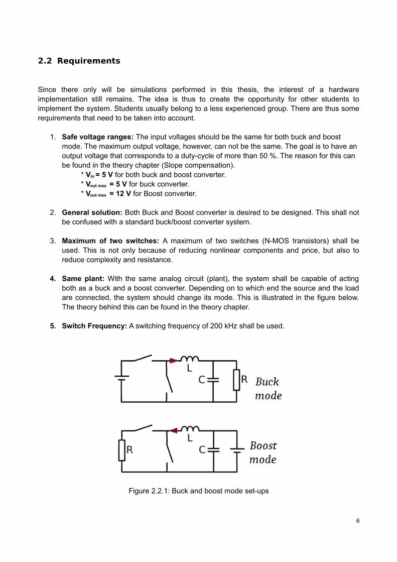
4. Same plant: With the same analog circuit (plant), the system shall be capable of actingboth as a buck and a boost converter. Depending on to which end the source and the loadare connected, the system should change its mode. This is illustrated in the figure below.The theory behind this can be found in the theory chapter.
5. Switch Frequency: A switching frequency of 200 kHz shall be used.
6
Figure 2.2.1: Buck and boost mode set-ups

7

3 THEORY
3.1 Introduction
In this chapter, the theory behind both buck and boost converters will be given. At first, basic andgeneral theory with simple set-ups will be presented to introduce the reader. Later on, a moredetailed explanation will be given, with the goal to specifically describe current-mode DC-DCconverters. When current mode control is understood, a deeper mathematical model and analysisis given. Another interesting phenomenon is subharmonic oscillation. The problem and solution forthis phenomenon are found in this chapter as well. Current mode control suffers from Subharmonicoscillation and a standard solution is called “slope compensation”. Even if slope compensation isnot implemented in any of the models in this work, the theory behind it is still of interest. This isbecause it will be an important part of the discussion chapter.
3.2 Basic theory
The absolute easiest way of describing a Buck converter is done with the concept of pulse widthmodulation (PWM). By switching a transistor on and off, the level of the output voltage will directlybe related to the duty cycle. However, switching a transistor will generate an output voltage thatcontains high-frequency components. This is due to the relatively sharp edges, when toggling theswitch. A solution to this is thus a low-pass filter, connected to the switch. In the following pages,the relations for both buck and boost converters will be derived.
8

Buck converter relations
To begin simple, steady state mode is assumed during this derivation. Steady state means thatthe current in the inductor never fall to zero. The picture below shows a buck converter set-upwhere the switch is either closed or open. When the switch is closed, the voltage across theinductor is given by equation (1). When the switch is open, the voltage across the inductor is givenby equation (2). (Note: The voltage drop across the diode is ignored for simplicity).
V L=V i−V o (1)
V L=−V o (2)
The voltage across an inductor is given as
V L=L⋅dI Ldt
(3)
This gives the charging current:
∇I L(ON )=∫0
D⋅TV L
Ldt=∫
0
D⋅TV i−V o
Ldt=
V i−V o
L⋅D⋅T (4)
And the discharge current:
∇I L(OFF )=∫D⋅T
TV L
Ldt=
−V o
L⋅(1−D)⋅T (5)
Since steady state condition is assumed, the following relations can be used:
∇ I L(ON )+∇ I L(OFF )=0 ⇔ D⋅T⋅V i−V o
L−V o
L⋅(1−D)⋅T=0 ⇒ D⋅V i=V o (6)
This gives the well known relation
D=V o
V i
(7)
9
Figure 3.2.1:Buck converter during ON and OFF states of the switch
Boost converter relations
Like the basics for the buck converter, steady state mode is assumed here as well. The picturebelow shows a boost converter set-up where the switch is either closed or open. When the switchis closed, the voltage across the inductor is given by equation (8). When the switch is open, thevoltage across the inductor is given by equation (9). (Note: The voltage drop across the diode isignored for simplicity).
V L=V i (8)
V L=V i−V o (9)
The voltage across an inductor is given as
V L=L⋅dI Ldt
(10)
This gives the charging current:
∇I L(ON )=∫0
D⋅TV L
Ldt=∫
0
D⋅TV i
Ldt=
V i
L⋅D⋅T (11)
And the discharge current:
∇I L(OFF )=∫D⋅T
TV L
Ldt=
V i−V o
L⋅(1−D)⋅T (12)
Since steady state condition is assumed, the following relations can be used:
∇ I L(ON )+∇ I L(OFF )=0 ⇔ D⋅T⋅V i
L+V i−V o
L⋅(1−D)⋅T=0 ⇒ ...⇒ 1
1−D=V o
V i
(13)
This gives the duty cycle
D=1−V i
V o
(14)
10
Figure 3.2.2:Boost converter during ON and OFF states of the switch
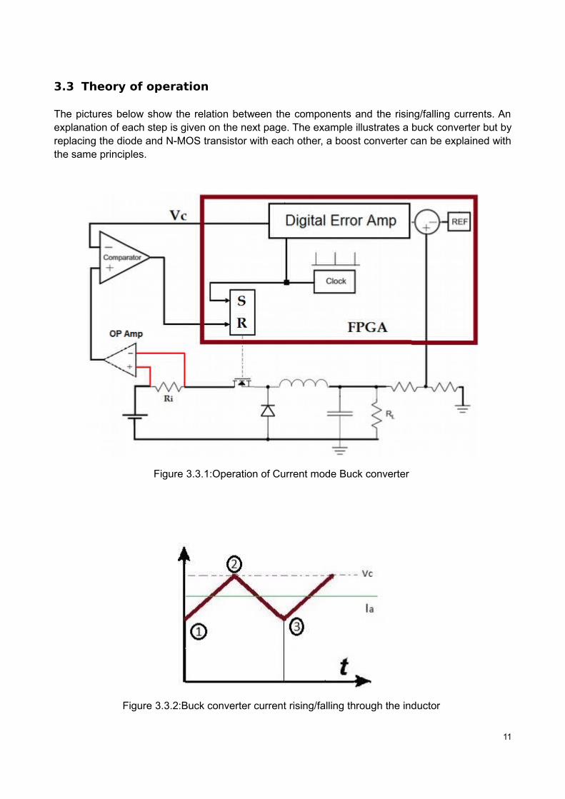
3.3 Theory of operation
The pictures below show the relation between the components and the rising/falling currents. Anexplanation of each step is given on the next page. The example illustrates a buck converter but byreplacing the diode and N-MOS transistor with each other, a boost converter can be explained withthe same principles.
11
Figure 3.3.1:Operation of Current mode Buck converter
Figure 3.3.2:Buck converter current rising/falling through the inductor

The pictures on the previous page show an overview of each step in an operation cycle. For simplicity, one can assume the voltage V c (control voltage) to be constant.
1. Clock trigs the SR-latch. This turns the N-MOS transistor on. When the Transistor is on, theinductor current starts to rise.
2. The voltage over Ri increases, which is amplified by the OP-Amp. The output of this amplifier has now a voltage that is greater than V c . This trigs the comparator which resetsthe SR-latch. The inductor current starts to discharge.
3. The clock trigs the SR-latch again and a new cycle is repeated.
Error amplifier
In a real application, the load resistance can vary. Changes in load resistance will also affect thevoltage over it. As seen in figure 3.3.1, any change in the output voltage compared to a givenreference voltage will affect the error amplifier. The error amplifier will in its turn change the controlvoltage V c such that the desired output voltage (= reference voltage) is maintained.
Notes:
• The graph represents currents but is represented as voltages in hardware.
• The goal is to keep an average current ( Ia ) such that V out=Ia⋅RL
• The resistor Ri needs to have a low resistance. An amplifier is needed to sense the small voltage.
• The clock is a sample clock which determines the sample rates and switch frequency.
12
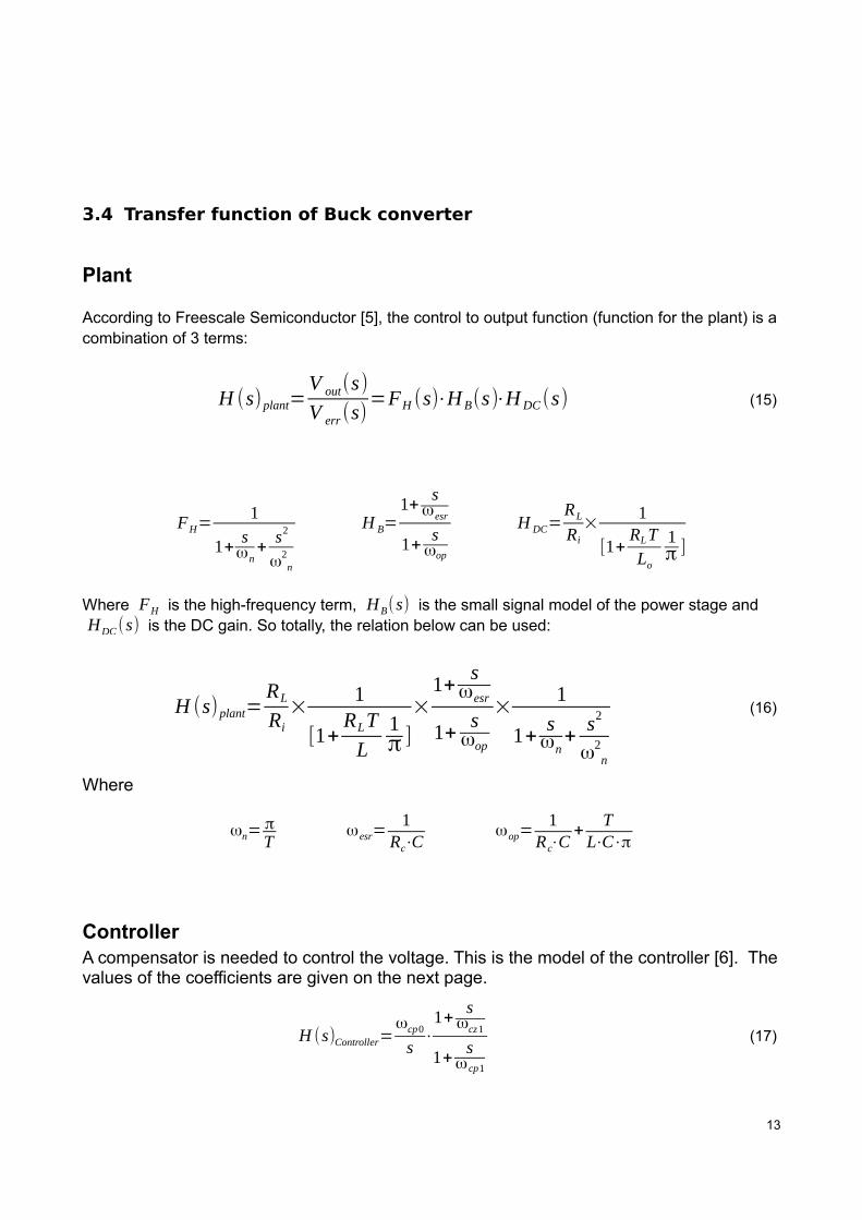
3.4 Transfer function of Buck converter
Plant
According to Freescale Semiconductor [5], the control to output function (function for the plant) is acombination of 3 terms:
H (s)plant=V out(s)
V err (s)=FH (s)⋅HB(s)⋅HDC(s) (15)
FH=1
1+sωn
+s2
ω2n
H B=1+
sωesr
1+s
ωop
H DC=RL
Ri
×1
[1+RLTLo
1π ]
Where FH is the high-frequency term, HB(s) is the small signal model of the power stage andHDC (s) is the DC gain. So totally, the relation below can be used:
H (s)plant=RL
Ri
×1
[1+RLT
L1π ]
×1+
sωesr
1+s
ωop
×1
1+sωn
+s2
ω2n
(16)
Where
ωn=πT
ωesr=1
Rc⋅C ωop=
1Rc⋅C
+T
L⋅C⋅π
ControllerA compensator is needed to control the voltage. This is the model of the controller [6]. Thevalues of the coefficients are given on the next page.
H (s)Controller=ωcp0
s⋅
1+s
ωcz1
1+s
ωcp1
(17)
13
Whole System
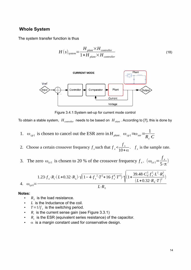
The system transfer function is thus
H (s)system=H plant×H controller
1+H plant×H controller
(18)
To obtain a stable system, H controller needs to be based on H plant . According to [7], this is done by
1. ω cp1 is chosen to cancel out the ESR zero inH plant . ω cp1=ω esr=1
Rc⋅C
2. Choose a certain crossover frequency f x such that f x<f s
10+α. f s is the sample rate.
3. The zero ωcz1 is chosen to 20 % of the crossover frequency f x . (ωcz 1=f x
5⋅π)
4. ωcp 0=
1.23⋅f x⋅Ri⋅(L+0.32⋅RL)⋅√(1− 4⋅f x2⋅T 2+16⋅f x
4⋅T 4)⋅√(1+39.48⋅C0
2⋅f x
2⋅L2
⋅RL2
(L+0.32⋅RL⋅T )2
)
L⋅RL
Notes:• RL is the load resistance.• L is the Inductance of the coil.• T=1/ f s is the switching period.• Ri is the current sense gain (see Figure 3.3.1)• Rc is the ESR (equivalent series resistance) of the capacitor.• α is a margin constant used for conservative design.
14
Figure 3.4.1:System set-up for current mode control

Derivation of ωcp 0
To achieve the desired crossover frequency of f x , the gain of the controller ωcp 0 needs to be chosen based on f x . The crossover frequency occurs when
|H (i⋅f x )plant⋅H (i⋅f x )controller|=1 ⇔ |H DC (i⋅f x)⋅H B(i⋅f x)⋅FH (i⋅f x)⋅H (i⋅f x)controller|=1 (19)
By inserting equation (16) and (17) into (19), the result will be:
|RL
Ri
×1
[1+RLT
L1π ]
×1+
i⋅f xωesr
1+i⋅f xωop
×1
1+i⋅f xωn
+(i⋅f x)
2
ω2n
×ωcp 0
i⋅f x⋅
1+i⋅f xωcz 1
1+i⋅f xωcp1|=1 (20)
Since ωcp1 is chosen to cancel out ωesr , solving out ωcp 0 gives
ωcp0=Ri⋅f xRL
×[1+RLT
L1π ]×|1+
i⋅f xωop
|×|1+i⋅f xωn
+(i⋅f x)
2
ω2n|×| 1
1+i⋅f xωcz1
| (21)
Inserting the values of RL , Ri , L , T , Rc , ωcz 1 , ωn , ωop and the desired crossover frequency f xgives
ωcp 0=
1.23⋅f x⋅Ri⋅(L+0.32⋅RL)⋅√(1− 4⋅f x2⋅T 2
+16⋅f x4⋅T 4
)⋅√(1+39.48⋅C0
2⋅f x
2⋅L2
⋅RL2
(L+0.32⋅RL⋅T )2 )
L⋅RL
(22)
15

3.5 Transfer function of Boost converter
Plant
According to TI [8], the control to output function (function for the plant) is given by
H (s)plant=V out(s)
V err (s)=FH (s)⋅HB(s)⋅HDC(s) (23)
FH=1
1+sωn
+s2
ω2n
H B=(1+
sωesr
)×(1− sωrhp
)
1+sωp
H DC=RL
Ri
×(1−D)
Where FH is the high frequency term, HB(s) is the small signal model of the power stage andHDC (s) is the DC gain. So totally:
H Plant=RL
Ri
×(1−D)×(1+
sωesr
)×(1− sωrhp
)
1+sω p
×1
1+sωn
+s2
ω2n
(24)
Where
ωn=πT
ωesr=1
Rc⋅C ω p=
2C⋅RL
ωrhp=Rl
L
ControllerA compensator is needed to control the voltage. This is the model of the controller [9]. Thevalues of the coefficients are given on the next page.
H (s)Controller=ωcp0
s⋅
1+s
ωcz1
1+s
ωcp1
(25)
16

Whole System
The system transfer function is thus
H (s)system=H plant×H controller
1+H plant×H controller
(26)
To obtain a stable system, H controller needs to be based on H plant . According to [8], this is done by
1. ωcp 1=min(ωesr ,ωrhp)
2. f x=min(f s
10+α,ωrhp
2⋅π⋅
15+β
)
3. ωcz1=f x⋅2⋅π
5
4. ωcp0=1.23⋅f x⋅Ri
R (1−D)⋅√1− 4 f x
2⋅T 2
+16 f x4⋅T 4
⋅√1+(π⋅f x⋅C⋅R)2⋅√1+(
2π⋅f xωcp 1
)2
√1+(2π⋅f x⋅C⋅R )2⋅√1+(
2π⋅f x⋅L
R⋅(1−D)2 )
2
Notes:• The order of the steps 1 to 4 must be kept because of coefficient dependencies. • L is the coil Inductance, RL the load resistance and C the capacitance.• T=1/ f s is the switching period.• Ri is the current sense gain (see Figure 3.3.1)• Rc is the ESR (equivalent series resistance) of the capacitor.• α and β is margin constants used for conservative design. D is the duty cycle.
17
Figure 3.5.1:System set-up for current mode control

Derivation of ωcp 0
To achieve the desired crossover frequency of f x , the gain of the controller ωcp 0 needs to be chosen based on f x . The crossover frequency occurs when
|H (i⋅f x )plant⋅H (i⋅f x )controller|=1 ⇔ |H DC (i⋅f x)⋅H B(i⋅f x)⋅FH (i⋅f x)⋅H (i⋅f x)controller|=1 (27)
By inserting equation (24) and (25) into (27), the result will be:
|RL
Ri
×(1−D)×(1+
i⋅f xωesr
)×(1−i⋅f xωrhp
)
1+i⋅f xωop
×1
1+i⋅f xωn
+(i⋅f x)
2
ω2n
×ωcp0
i⋅f x⋅
1+i⋅f xωcz1
1+i⋅f xωcp 1|=1 (28)
Solving out ωcp 0 gives
ω cp0=Ri
RL
×f x
(1−D)×|1+
i⋅f xω n
+(i⋅f x)
2
ω2n
|×| 1+i⋅f xωop
1+i⋅f xω cz1
|× |1+i⋅f xω cp1
||1+ i⋅f x
ω esr|×|1− i⋅f xω rhp
| (29)
Inserting the values of RL , Ri , L , T , Rc , ωcz 1 , ωn , ωop , ωrhp and the desired crossover frequency f x gives
ω cp0=1.23⋅f x⋅Ri
R (1−D)⋅√ 1−4 f x
2⋅T2
+16 f x4⋅T 4
⋅√ 1+(π⋅f x⋅C⋅R )2⋅√ 1+(
2π ⋅f xωcp 1
)2
√ 1+(2π⋅f x⋅C⋅R )2⋅√ 1+(
2π ⋅f x⋅L
R⋅(1−D)2)
2(30)
OBS:
Depending on what value ωcp1 gets, |1+i⋅f xωcp1|will cancel out either |(1+
i⋅f xωesr
)| or |(1−i⋅f xωrhp
)|
18

3.6 Digital converter
So far, the model of both the plant and the controller are extracted. The model of the controller isthe most interesting part. But since the controller depends on the plant, both models need to beconsidered. For the analog designer, the controller coefficients ( ωcp 0 ωcp1 ωcz 1 ) can be directlyrelated to the capacitor and resistor values inside an analog controller [10]. For a digital designer, aconversion is needed to the desecrate time domain. This is done by 2 conversions:
1. Bilinear transformThis is done to move from the “s-plain” to “z-plain”
2. Inverse discrete Fourier transformThis is done to move to the discrete time domain.
Bilinear transform
According to [11], s can be approximated by:
s≈ 2T⋅z−1z+1
(31)
Inserting this into the controller will give
H (s)Controller=ωcp0
s⋅
1+s
ωcz1
1+s
ωcp1
⇒ H (2T⋅z−1z+1
)Controller
=ωcp0
2T⋅z−1z+1
⋅1+
2T⋅z−1z+1
ωcz 1
1+
2T⋅z−1z+1
ωcp1
(32)
Writing both he numerator and denominator on quadratic form with respect to Z gives
H controller=
Z2⋅T ωcp0 ωcp1(2+Tωcz1)
2(2+Tωcp1)ωcz1
+Z⋅ωcp0 ωcp 1⋅T
2
2(2+T ωcp1)+Tωcp0 ωcp1 (T ωcz 1− 2)
2(2+Tωcp1)ωcz1
Z2−Z⋅ 4(2+T ωcp1)
−Tωcp1−2(2+T ωcp1)
(33)
19

Inverse discrete fourier transformBy replacing the coefficients multiplied with Z, a standard discrete two-pole-two-zero controller is given:
H [Z ]=B0⋅Z
2+B1⋅Z+B2
Z2− Z⋅A1− A2
(34)
where
B0=Tωcp 0ωcp1(2+Tωcz1)
2(2+T ωcp1)ωcz1
B1=ωcp 0ωcp1⋅T
2
2 (2+Tωcp 1)
B2=T ωcp0 ωcp 1(Tωcz 1−2)
2(2+T ωcp1)ωcz1
A1=4
(2+T ωcp1)
A2=T ωcp1−2
(2+T ωcp1)
By knowing that
H [Z ]=Y [Z ]
X [Z ]=B0⋅Z
2+B1⋅Z+B2
Z2−Z⋅A1− A2
=B2⋅Z
−2+B1⋅Z
− 1+B0
− A2⋅Z−2− A1⋅Z
−1⋅+1
⇔
⇔ Y [ z ] (−A2⋅Z−2−A1⋅Z
−1⋅+1)=X [Z ](B2⋅Z
−2+B1⋅Z
−1+B0)
An inverse discreate fourier transform would lead to an LDE (linear difference equation).
−A2 y [n−2]−A1 y [n−1]+ y [n]=B2 x [n−2 ]+B1x [n−1]+B0 x [n] ⇔
y [n]=B2 x [n−2]+B1 x [n−1 ]+B0 x [n]+A2 y [n−2]+A1 y [n−1]
Notes:• x[n] denotes the error input to the controller • y[n] denotes the output of the controller• x[n-1] / y[n-1] denotes the input/output 1 sample ago• x[n-1] / y[n-1] denotes the input/output 2 samples ago
Implementation
20
The result of the transformations and derivations on previous page gave the following equation
y [n]=B2 x [n−2]+B1 x [n−1 ]+B0 x [n]+A2 y [n−2]+A1 y [n−1] (35)
Since y[n] (output of the controller) only depends on previous inputs and outputs of itself multiplied with coefficients, a digital implementation is possible.
Operations
The controller needs to be as fast as possible with its calculations. Ideally, the output should beready at the same time as the input is ready. From equation (35), one can see that 9 operations (4additions and 5 multiplications) are needed to be performed concurrently, whenever a new sampleis given. This is easy to achieve with FPGA:s. If a microcontroller is to be used, the relation mustbe separated in 2 parts:
y1[n ]=B2 x [n−2]+B1 x [n−1]+A2 y [n−2]+A1 y [n−1]
y [n]=y1[n]+B0 x [n ](36)
Where y1[n] is calculated in-between the samples and y[n] is calculated whenever x[n] is given.
This reduces the calculations to 1 addition and 1 multiplication. The other operations are calculated before each sample and thus ready to use.
21
Figure 3.6.1:Digital implementation of the controller
3.7 Subharmonic oscillation
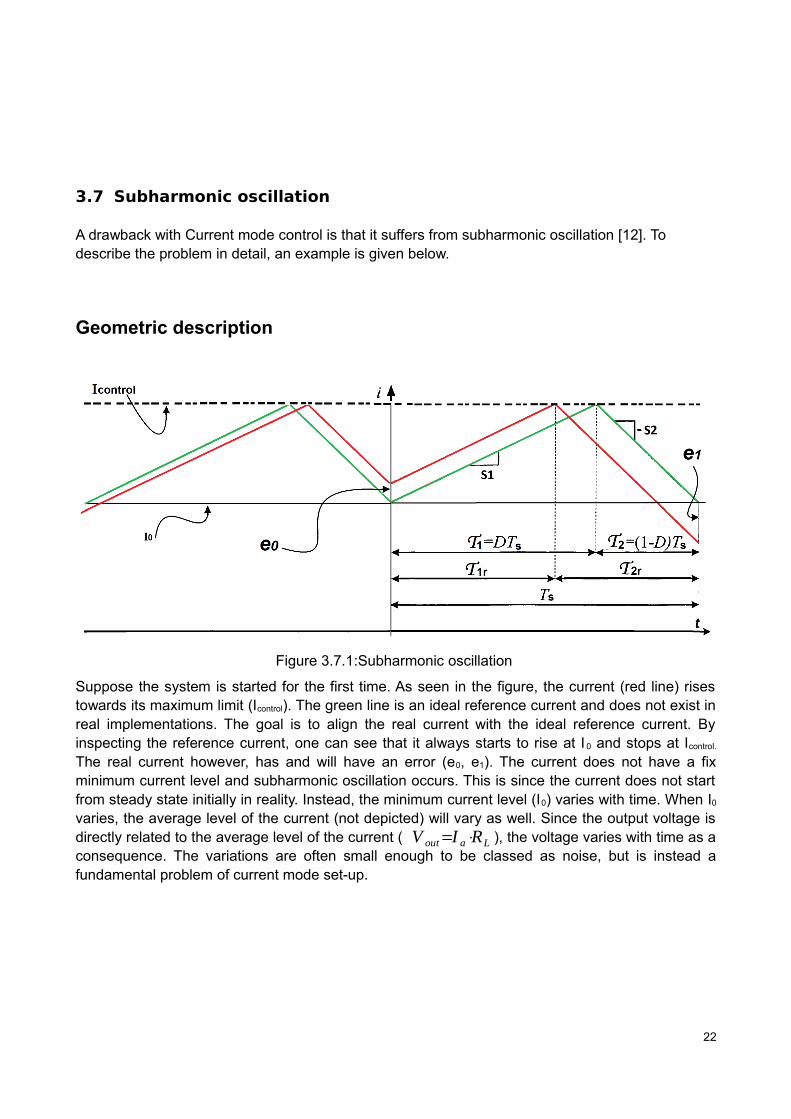
A drawback with Current mode control is that it suffers from subharmonic oscillation [12]. To describe the problem in detail, an example is given below.
Geometric description
Suppose the system is started for the first time. As seen in the figure, the current (red line) risestowards its maximum limit (Icontrol). The green line is an ideal reference current and does not exist inreal implementations. The goal is to align the real current with the ideal reference current. Byinspecting the reference current, one can see that it always starts to rise at I 0 and stops at Icontrol.
The real current however, has and will have an error (e0, e1). The current does not have a fixminimum current level and subharmonic oscillation occurs. This is since the current does not startfrom steady state initially in reality. Instead, the minimum current level (I0) varies with time. When I0
varies, the average level of the current (not depicted) will vary as well. Since the output voltage isdirectly related to the average level of the current ( V out=I a⋅RL ), the voltage varies with time as aconsequence. The variations are often small enough to be classed as noise, but is instead afundamental problem of current mode set-up.
22
Figure 3.7.1:Subharmonic oscillation

Algebraic description
By looking at figure 3.7.1, one can see the following relations:
(1) I control=I 0+m1⋅T 1 ⇔ T 1=I control−I 0
m1
(2) I control−m2⋅T2=I 0 ⇔ T2=I control−I 0
m2
(3) I control=I 0+e0+m1⋅T 1 r ⇔ T1 r=I control−I0−e0
m1
(4) i−m2⋅T2r=I 0+e1 ⇔ T 2 r=I control−I 0−e 2
m2
(5) T s=T 1 r+T 2 r=T 1+T 2
Inserting (1), (2), (3), (4) into (5) gives
I control−I 0−e0
m1
+I control−I 0−e 2
m2
=I control−I 0
m1
+I control−I 0
m2
⇔ e0
m1
=−e1
m2
⇔
⇔ e1=−m1
m2
⋅e0
(37)
This can be generalized to
en=(−m1
m2
)
n
⋅e0 (38)
For steady state condition, the relation below can be used:
m2
m1
=D
1−D(39)
It can be seen that when D < 50 %, then m1/m2 will decrease towards zero. This will cancel out the error e0, which will lead to an inductor current that settles. For D > 50 %, subharmonic oscillation occurs.
23

3.8 Slope compensation
A solution to subharmonic oscillation is called slope compensation [13]. Just as in the case of the problem, a geometrical description is given followed by algebraic relations.
Suppose the system is started for the first time. As seen in the figure, the real current (red line)rises towards its maximum limit Icontrol. The green line is only an ideal reference current, just like thecase of previous geometrical description. The goal is to align the real current with the idealreference current here as well. The difference is that the maximum current limit Icontrol (black line) isvarying with time. Note that whenever the real current reaches the maximum current limit, it startsto decrease. By inspecting the figure, one can see that the real current aligns itself with the idealreference current. This type of slope compensation is linear, which can be seen in the figure. Thereare other types such as quadratic slope compensation. For simplicity, only linear slopecompensation is discussed.
Notes:
• The real current settles within one switching cycle. This is called dead beat.
• The average value of the compensation ramp is the same as Icontrol would be without slope compensation.
24
Figure 3.8.1:Compensated system

Algebraic description
By looking at the figure below, one can see the following relations:
e0=m1⋅T d+mc⋅T d
e1=−(m2⋅T d−mc⋅T d )
e1
e0
=m2−mc
m1+mc
⇔ e1=−m2−mc
m1+mc
⋅e0
This can be generalized to en=(−m2−mc
m1+mc
)n
⋅e0
Notes:
• If mc = m2, the perturbed current will align itself with the steady state current within one switching cycle. This is called dead beat.
• If mc > m2 such that 0 < mc – m2 < 1, the perturbed current will align itself but after more than 1 switching cycle.
• If mc > m2 such that mc – m2 > 1, the perturbed current will not align itself and subharmonic oscillation occurs.
• The average value of the compensation ramp should be the same as the control voltage
25
Figure 3.8.2:Slope compensation

26

4 METHOD
4.1 Introduction
The way this thesis is performed can be seen as an iterative process. The work starts at atheoretical level and the first goal is a mathematical model that describes the system. In latersteps, a simulation model will be built and improved for each step. Between these steps,measurements will take place. The results of all measurements can be found in the result chapter.Since the simulation models are a result of the work, they will be presented in the results chapteras well. In this chapter, the methods used are described. This chapter can also be seen as a “stepby step” guide, for the interested readers to perform the same work and measurements. Totally,there will be 4 implementation iterations. Each iteration has a
• Work method: Method used to create the simulation models, presented in the resultchapter.
• Measurement method: A description of how the measurements are performed on thesimulation models.
• Goal: The goal of each implementation iteration is described here. This is to help thereader maintain an overview of the work done.
• Comments: If needed, comments are given to clarify and avoid misunderstandings.
27

4.2 Used Design method
Component values of the plant will be considered first. The theory chapter and otherdesigns found in the literature with similar input/output voltages will be used. When thecomponent values of the plant are found, the controller will be designed. The theory chapterwill be used during the design of the controller.
4.3 Used measurement method
Two types of measurements are of interest, the frequency response and the “combined step response”
• Frequency response: The frequency response of the open-loop system is of interest. This is the same as the frequency response of both the plant and the controller combined. The open-loop frequencyresponse gives the phase-margin, gain-margin and crossover frequency. These parameterstell how fast and stable the system is.
• Combined step response: The response of a step in both voltage and current are of interest. First, the desired output voltage is increased (Vref to the controller), to see how much time and overshoot it takes to reach the desired voltage. Then, the required load current is increased, to see how much time and voltage drop it takes for the system to maintain the desired output voltage.
28
Figure 4.2.1: Method and work flow

As seen in the picture above, 2 voltage levels (voltage steps) are of interest. The first voltagecorresponds to a duty cycle less than 50 % and the higher voltage corresponds to a duty cyclehigher than 50 %. For each voltage level, a step load is performed. This is done by reducing (orincreasing) the load, increasing the need of more current, to maintain the same output voltage. Thepicture above will also act as a reference response, since it is illustrating the ideal case (no delaysin steps, no voltage drops etc.). Vout and Iout for buck and boost mode are given in the list below.The reason of the chosen voltages/currents to test with is discussed in the background chapter.
Vin Vout1 Vout2 Iout1 Iout2 Iout3 Iout4
Buck 5 V 1 V 4.5 V 0.1 A 0.2 A 0.45 A 0.9 A
Boost 5 V 6 v 12 v 0.5 A 1 A 1 A 2 A
Table 4.1: Voltages and currents used during the measurements.
29
Figure 4.3.1: Combined step response
4.4 Implementation
Totally there are 4 work iterations. Each iteration is described here in detail.
Work iteration 1
• Working method: Use the theory chapter and the literature to create a system model with the same system behavior as described in the Background chapter.
• Measurement method: Measure the open loop frequency response when the model is done. A detailed description of open-loop frequency response is given under “Used measurement method”.
• Goal: The goal is a mathematical model of both the plant and the controller.
• Comments: The work during this step is rather a research than implementation.
Work iteration 2
• Working method: Change the mathematical model of the plant to a Simulink model with components from the Simulink package Simscape (resistor, capacitor, inductor and load). Use the same mathematical model of the controller as used in the previous step. During theconversion to a Simulink model, use the theory chapter.
• Measurement method: Measure the “combined step response” when the model is done. Adetailed description of “combined step response” is given under “Used measurement method”.
• Goal: The goal is a model where the plant is a Simulink model and the controller is a mathematical model.
Work iteration 3
• Working method: Change the mathematical model of the controller to a Simulink model with components from the Simulink package “commonly used blocks”. Use the same Simulink model for the plant as used in the previous step. During the conversion to a Simulink model, use the theory chapter.
• Measurement method: Measure the “combined step response” when the model is done. Adetailed description of “combined step response” is given under “Used measurement method”.
• Goal: The goal is to create a model where both the plant and controller consists of Simulinkcomponents (system without mathematical parts).
30

Work iteration 4
• Working method: Increase the plant model with the following components:
1. ADC with data transfer delay and a bit accuracy of 10 bits. An Appropriate Vref voltage should be used such that functionality is maintained.
2. DAC with data transfer delay and a bit accuracy of 10 bits. An Appropriate Vref voltage should be used such that functionality is maintained.
3. Resistive divider, which is needed at the input of the ADC.
4. Introduce delays to the switches (10^-8 s)
Increase/change the model of the controller with the following components:
1. Softstart block, such that instability is avoided
2. Voltage dividers needed because of the DAC, ADC and resistive divider.
3. Change all blocks from Simulink blocks to “ALTERA DSP builder” blocks (VHDL blocks).
4. Introduce calculation delays of 1 clock cycles in the controller.
• Measurement method: Simulate the model until
• Minimum bit accuracy (needed for the controller) is found
• Minimum clock frequency of the system if found
• Goal: The goal is to create a model that behaves as realistic as possible.
• Comments: There are no components such as ADC or DAC in Simulink. Thus, a modelthat behaves as an ADC/DAC is to be built. The “data transfer delays” are introduced sincethe ADC/DAC data is transferred in serial. “An appropriate Vref voltage” means a Vrefvoltage that maintains functionality but is still realistic. A bit accuracy of 10 bits is chosensince it is considered to be realistic and common. Switch and calculation delays arepredicted to be close to the given values, if implemented in real hardware.
31

32
5 RESULTS
5.1 Introduction
In this chapter, the result of all designs and measurement are given. Each design has its ownmeasurements as described in the method chapter. Totally there are eight design results with acorresponding measurement result. At the end of this chapter, subsystems used in the designs aregiven. Since the controller inside model 4 (both Buck and Boost designs) is containing VHDLblocks, only the block names are given. The VHDL code for all blocks can be found in APPENDIX.
5.2 Design and Measurement results
In the following pages, both design and measurement results are given. The first four results aregiven for the Buck converter and the following four is Boost converter results. Each result containsthe following information:
1. Model of the Plant
2. Model of the controller.
3. Coefficients used in the models.
4. Measurement result (frequency response or combined step response)
33
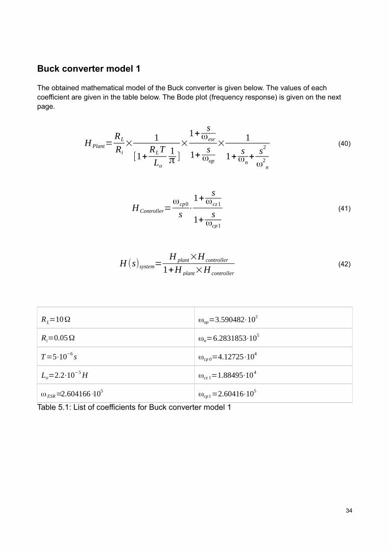
Buck converter model 1
The obtained mathematical model of the Buck converter is given below. The values of each coefficient are given in the table below. The Bode plot (frequency response) is given on the next page.
H Plant=RL
Ri
×1
[1+RLT
Lo
1π ]
×1+
sωesr
1+s
ωop
×1
1+sωn
+s2
ω2n
(40)
HController=ωcp0
s⋅
1+s
ωcz1
1+s
ωcp1
(41)
H (s)system=H plant×H controller
1+H plant×H controller
(42)
RL=10Ω ωop=3.590482⋅102
Ri=0.05Ω ωn=6.2831853⋅105
T=5⋅10−6 s ωcp 0=4.12725⋅104
Lo=2.2⋅10−5H ωcz 1=1.88495⋅104
ω ESR=2.604166⋅105ωcp1=2.60416⋅105
Table 5.1: List of coefficients for Buck converter model 1
34
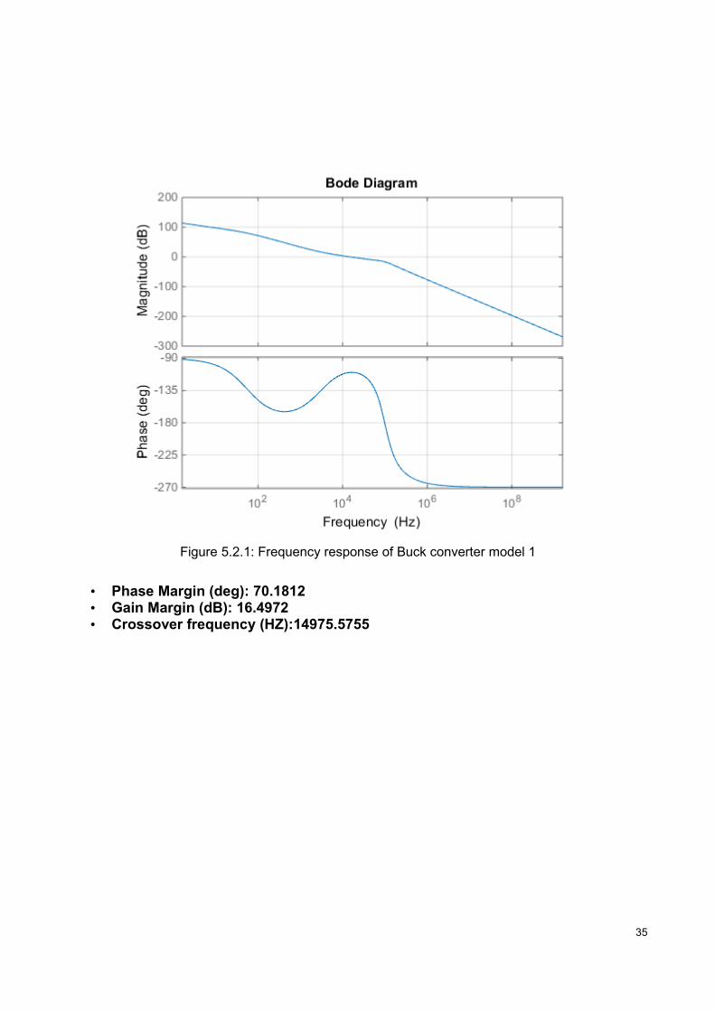
• Phase Margin (deg): 70.1812• Gain Margin (dB): 16.4972• Crossover frequency (HZ):14975.5755
35
Figure 5.2.1: Frequency response of Buck converter model 1

Buck converter model 2
The model of the Plant is given in the figure. The coefficients are given in the table.
L=2.2⋅10−5 H T Switch(ON)=0.001ns Ri=0.05Ω C=4.8⋅10− 4 F
LESR=0.1Ω Rswitch(ON )=0.1Ω Rswitch(OFF )=108Ω CESR=8mΩ
Table 5.2: Coefficients used inside the Plant in Buck converter model 2.
36
Figure 5.2.2: Model of the Plant, using Simulink components
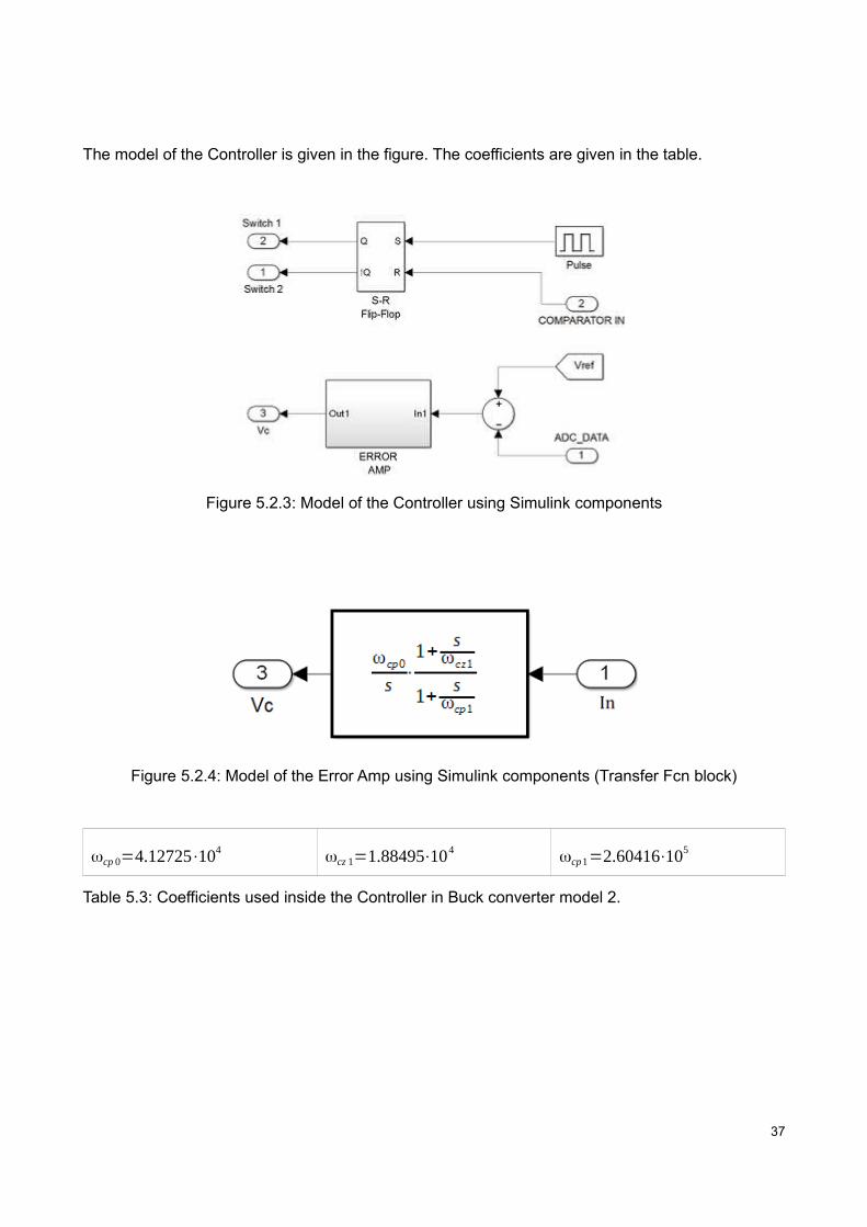
The model of the Controller is given in the figure. The coefficients are given in the table.
ωcp 0=4.12725⋅104ωcz 1=1.88495⋅104
ωcp1=2.60416⋅105
Table 5.3: Coefficients used inside the Controller in Buck converter model 2.
37
Figure 5.2.3: Model of the Controller using Simulink components
Figure 5.2.4: Model of the Error Amp using Simulink components (Transfer Fcn block)
38
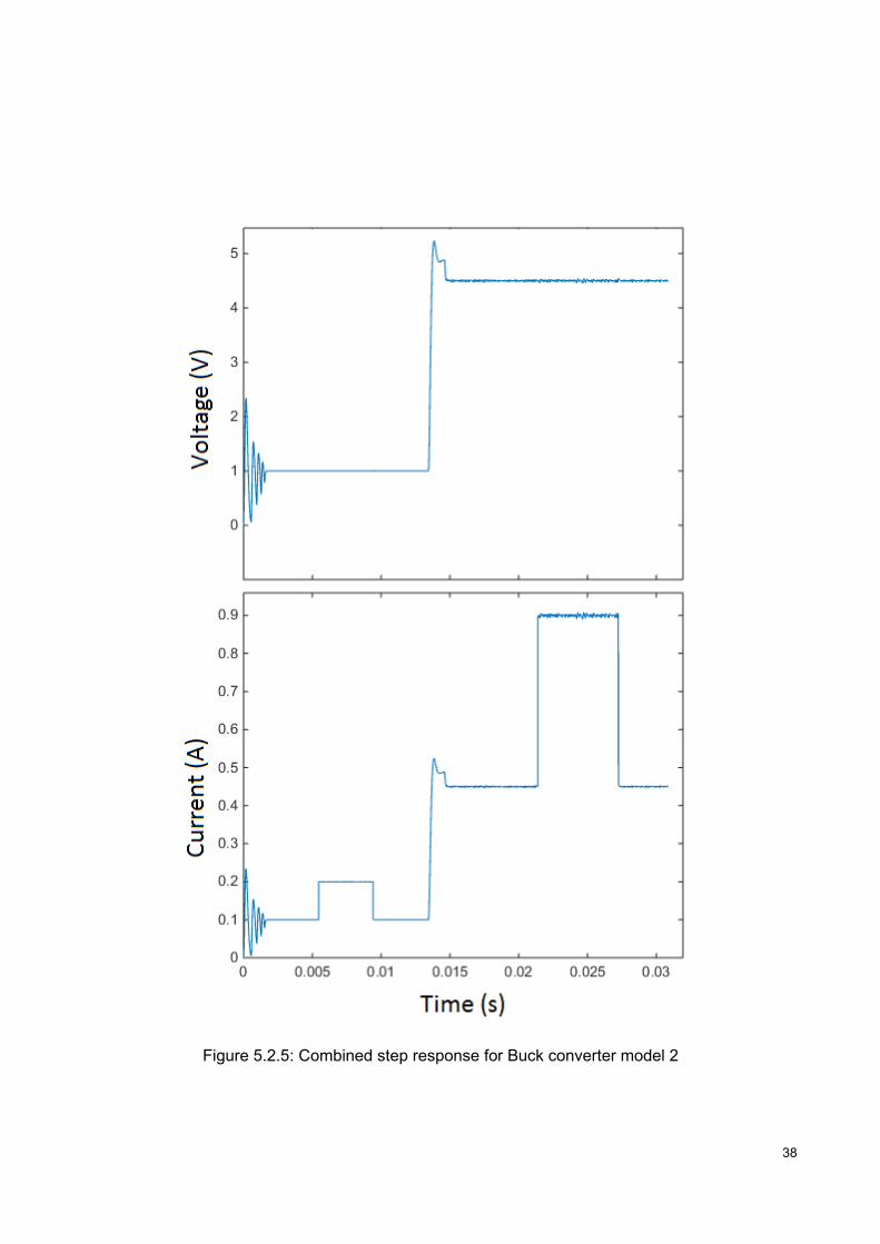
Figure 5.2.5: Combined step response for Buck converter model 2
Buck converter model 3
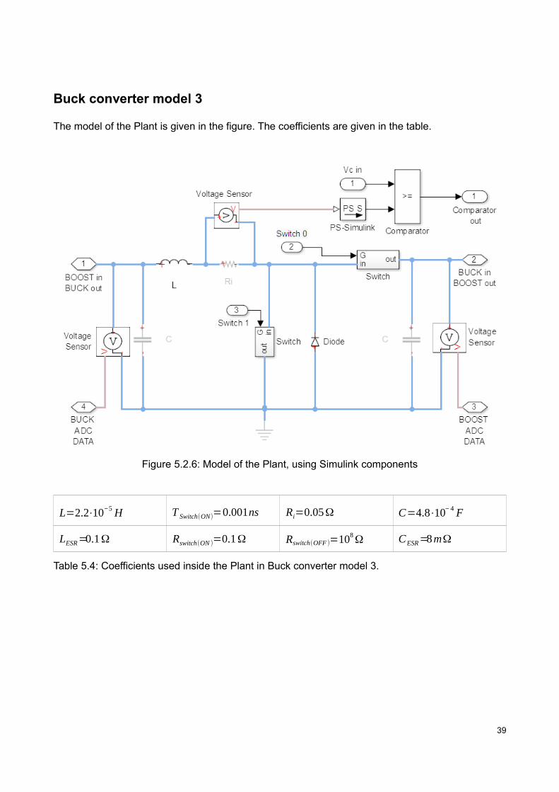
The model of the Plant is given in the figure. The coefficients are given in the table.
L=2.2⋅10−5 H T Switch(ON)=0.001ns Ri=0.05Ω C=4.8⋅10− 4 F
LESR=0.1Ω Rswitch(ON )=0.1Ω Rswitch(OFF )=108Ω CESR=8mΩ
Table 5.4: Coefficients used inside the Plant in Buck converter model 3.
39
Figure 5.2.6: Model of the Plant, using Simulink components

The model of the Controller is given in the figure. The coefficients are given in the table.
B0=0.90408 B1=0.08137 B2=−0.82271
A 1=1.21135 A 2=−0.21135 Zdelay=510−6 s
Table 5.5: Coefficients used inside the Controller in Buck converter model 3.
40
Figure 5.2.7: Model of the Controller using Simulink components
Figure 5.2.8: Model of the Error Amp using Simulink components

41
Figure 5.2.9: Combined step response for Buck converter model 3

Buck converter model 4
The model of the Plant is given in the figure. The coefficients are given in the table on next page.
42
Figure 5.2.10: Model of the Plant, using Simulink components
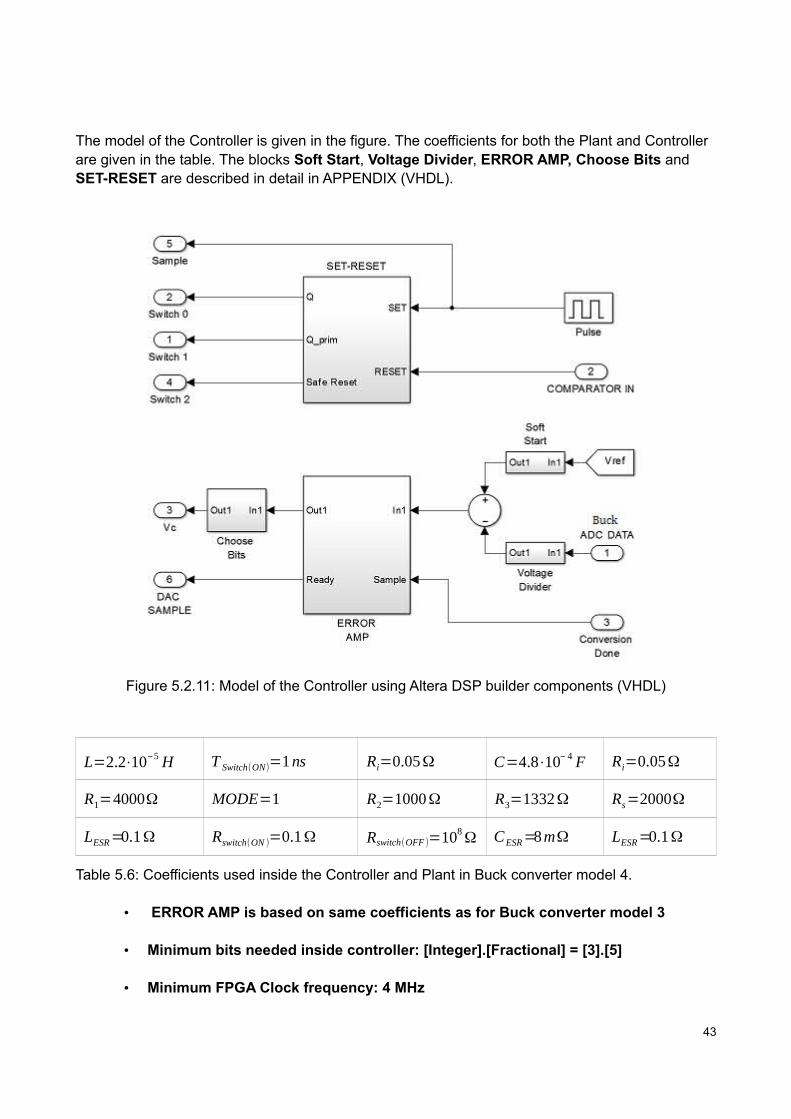
The model of the Controller is given in the figure. The coefficients for both the Plant and Controller are given in the table. The blocks Soft Start, Voltage Divider, ERROR AMP, Choose Bits and SET-RESET are described in detail in APPENDIX (VHDL).
L=2.2⋅10−5 H T Switch(ON)=1ns Ri=0.05Ω C=4.8⋅10− 4 F Ri=0.05Ω
R1=4000Ω MODE=1 R2=1000Ω R3=1332Ω Rs=2000Ω
LESR=0.1Ω Rswitch(ON )=0.1Ω Rswitch(OFF )=108Ω CESR=8mΩ LESR=0.1Ω
Table 5.6: Coefficients used inside the Controller and Plant in Buck converter model 4.
• ERROR AMP is based on same coefficients as for Buck converter model 3
• Minimum bits needed inside controller: [Integer].[Fractional] = [3].[5]
• Minimum FPGA Clock frequency: 4 MHz
43
Figure 5.2.11: Model of the Controller using Altera DSP builder components (VHDL)
44
Figure 5.2.12: Combined step response for Buck converter model 4

Boost converter model 1
The obtained mathematical model of the Boost converter is given below. The values of each coefficient are given in the table below. The Bode plot (frequency response) is given on the next page.
H Plant=K dc×(1+
sω esr
)×(1− sω rhp
)
1+s
ω p
×1
1+sω n
+s2
ω 2n
(43)
HController=ωcp0
s⋅
1+s
ωcz1
1+s
ωcp1
(44)
H (s)system=H plant×H controller
1+H plant×H controller
(45)
Kdc=50 ωp=6.94444102
ωrhp=4.73484104ωn=6.28318⋅105
ωcp1=4.73484⋅104 ωcp 0=100
ω ESR=2.60416⋅105ωcz 1=1.51515⋅103
Table 5.7: List of coefficients for Boost converter model 1
45

• Phase Margin (deg): 68.714• Gain Margin (dB): 26.9616• Crossover frequency (HZ):408.804
46
Figure 5.2.13: Frequency response of Boost converter model 1

Boost converter model 2
The model of the Plant is given in the figure. The coefficients are given in the table.
L=2.2⋅10−5 H T Switch(ON)=0.001ns Ri=0.05Ω C=4.8⋅10− 4 F
LESR=0.1Ω Rswitch(ON )=0.1Ω Rswitch(OFF )=108Ω CESR=8mΩ
Table 5.8: Coefficients used inside the Plant in Boost converter model 2.
47
Figure 5.2.14: Model of the Plant, using Simulink components
The model of the Controller is given in the figure. The coefficients are given in the table.
ωcp1=4.73484⋅104ωcz 1=1.51515⋅103 ωcp 0=100
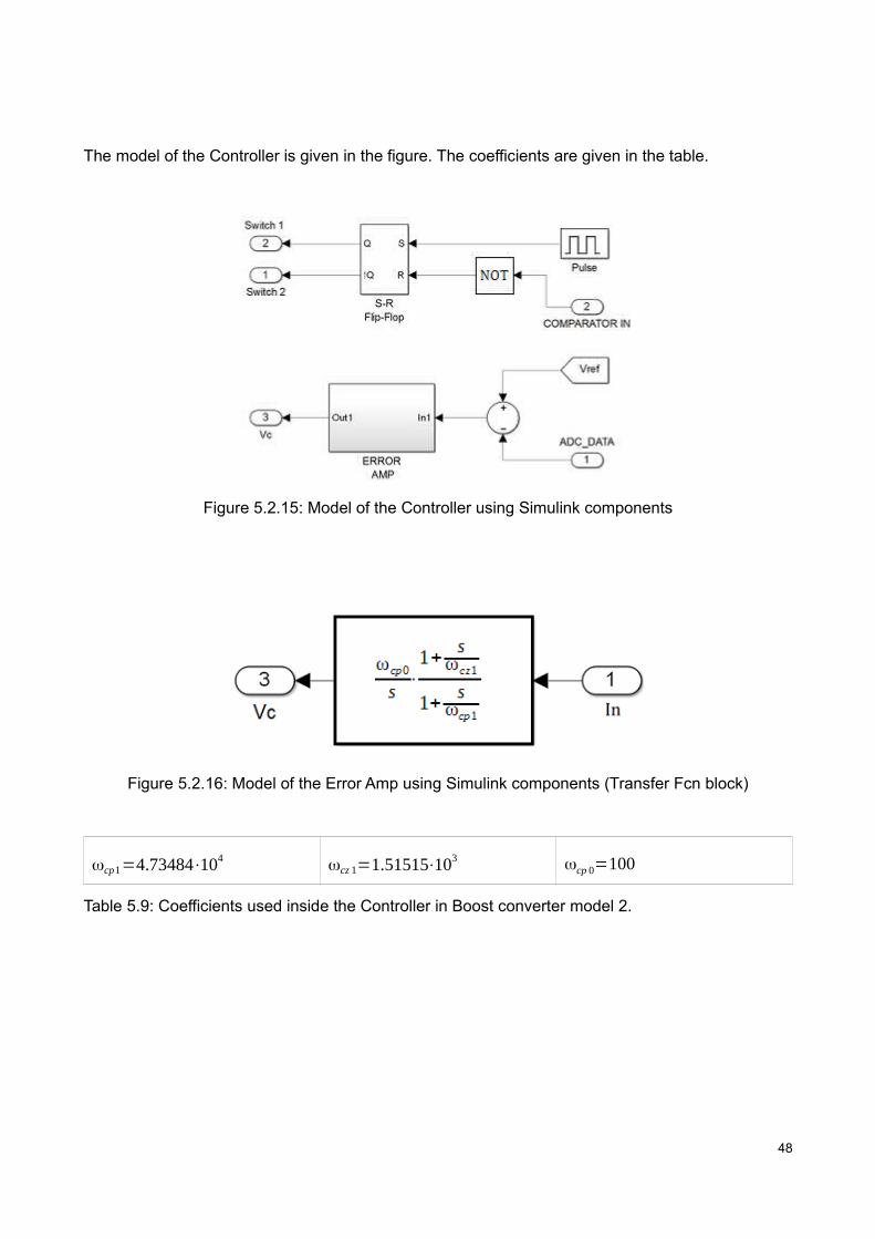
Table 5.9: Coefficients used inside the Controller in Boost converter model 2.
48
Figure 5.2.15: Model of the Controller using Simulink components
Figure 5.2.16: Model of the Error Amp using Simulink components (Transfer Fcn block)

49
Figure 5.2.17: Combined step response for Boost converter model 2

Boost converter model 3
The model of the Plant is given in the figure. The coefficients are given in the table.
L=2.2⋅10−5 H T Switch(ON)=0.001ns Ri=0.05Ω C=4.8⋅10− 4 F
LESR=0.1Ω Rswitch(ON )=0.1Ω Rswitch(OFF )=108Ω CESR=8mΩ
Table 5.10: Coefficients used inside the Plant in Boost converter model 3.
50
Figure 5.2.18: Model of the Plant, using Simulink components

The model of the Controller is given in the figure. The coefficients are given in the table.
B0=0.0070120660 B1=5.292125317⋅10−5 B2=−0.0069591447
A 1=1.7883149872 A 2=−0.7883149872 Zdelay=0.000005
Table 5.11: Coefficients used inside the Controller in Boost converter model 3.
51
Figure 5.2.19: Model of the Controller using Simulink components
Figure 5.2.20: Model of the Error Amp using Simulink components

52
Figure 5.2.21: Combined step response for Boost converter model 3

Boost converter model 4
The model of the Plant is given in the figure. The coefficients are given in the table on next page.
53
Figure 5.2.22: Model of the Plant, using Simulink components

The model of the Controller is given in the figure. The coefficients for both the Plant and Controller are given in the table. The blocks Soft Start, Voltage Divider, ERROR AMP, Choose Bits and SET-RESET are described in detail in APPENDIX (VHDL).
L=2.2⋅10−5H T Switch(ON )=1ns Ri=0.05Ω C=4.8⋅10−4 F Ri=0.05Ω
R1=4000Ω MODE=2 R2=1000Ω R3=1332Ω Rs=2000Ω
LESR=0.1Ω Rswitch (ON )=0.1Ω Rswitch (OFF )=108Ω CESR=8mΩ LESR=0.1Ω
Table 5.12: Coefficients used inside the Controller and Plant in Boost converter model 4.
• ERROR AMP is based on same coefficients as for Boost converter model 3
• Minimum bits needed inside controller: [Integer].[Fractional] = [5].[20]
• Minimum FPGA Clock frequency: 4 MHz
54
Figure 5.2.23: Model of the Controller using Altera DSP builder components (VHDL)

55
Figure 5.2.24: Combined step response for Boost converter model 4

5.3 Used Subsystems
The following pages will describe the used subsystems seen inside the models. A short description is also given (if needed).
Switch
The used switches (acting as NMOS transistors) are containing following components.
• OBS: Transport Delay is changed by changing the coefficient T Switch(ON ) .
Single Piulse
• Unit delay = 1 FPGA clock cycle
• Output pulse will have a duration of 1 FPGA clock cycle.
56
Figure 5.3.1: Components inside the Switch blocks.
Figure 5.3.2: Components inside the Single Pulse blocks

ADC
The ADC introduces a quantization error (quantization block). It also introduces a delay before the data is reached to the controller. It takes [ADC_BITS] clock cycles for the data to reach the controller, when the voltage is sampled.
Notes:
• DFF ALTERA block consists of a Data flip flop from DSP builder package.
• All voltages above Vref_ADC will be presented as Vref_ADC
• All negative voltages will be presented as 0.
57
Figure 5.3.3: Components inside the ADC blocks.

DAC
The DAC introduces a quantization error (quantization block). It also introduces a delay before the data is reached to the comparator. It takes [DAC_BITS] clock cycles for the datato reach the Comparator, when the digital value is sampled.
Notes
• DFF ALTERA block consists of a Data flip flop from DSP builder package
• Since a DAC normally takes input from 0 up to 2^BAC_BITS, a voltage divider is used at the input to create the same effect.
• Since the ADC quantizer has an output D=A
Vref Dac×2DacBits , a voltage divider
is used at the output to cancel out the ADC effect.
58
Figure 5.3.4: Components inside the DAC blocks.

Voltage Divider (Inside DAC)
Performs a multiplication needed to create a DAC from ADC quantizer block.
BUCK/BOOST SWITCH
Since the same Plant is used, Both for Buck and Boost mode, the voltage over Ri will become negative during Buck mode. This is a problem since the DAC only can represent positive values. Thus a switch that flips the polarity of the voltage over the resistor Ri is needed.
59
Figure 5.3.5: Components inside the Voltage Divider blocks.
Figure 5.3.6: Components inside the BUCK/BOOST SWITCH block.

60

6 DISCUSSION
6.1 Results
Buck converter
By taking a look at the bode plot of the buck converter, it is clearly seen that the gain margin,phase margin and crossover frequencies are in a “good range”. The system is stable enough sinceGm > 20 dB and Pm > 45 degrees. It is also seen that this stability is achieved at a crossoverfrequency of 15000 Hz. This is quite good since it makes the system fast. The speed of thesystem is also demonstrated by looking at the combined step-responses. One can observe thefollowing:
• When the need of current is doubled, there is no voltage drop to observe.
• The time it takes for the currents to rise/fall to its final value is comparable with an ideal case (see combined step-response in method chapter)
• The buck converter is, however, suffering from an overshot, when the reference voltage is changed (voltage step). It also suffers from sub-harmonic oscillation. This can be seen by observing the “noise” when the voltage is 4.5 V (D > 50 %).
• It is also seen that the sub-harmonic oscillation is increased when looking at model 4. This is due to the quantization noise (from the ADC and DAC). The quantization noise can also be observed by looking at the output voltage when Vo = 1 V (D < 50 %).
61

Buck converter Softstart
The most interesting thing to observe in model 4 is the softstart. Softstart is needed here since theADC (and DAC) is not capable of representing the overshoots. But softstart does not onlydecrease the overshoots, it is also quite fast. This speed can be increased even further, since it isa digital softstart. The cost of this increase in speed is a small (or larger) overshoot, depending onhow fast one wish the system to be.
Boost Converter
By taking a look at the bode-plot of the Boost converter, it is clearly seen that the stability is good.Both gain margin and phase margin lay in the appropriate intervals (gm >10 dB & Pm > 45 deg).However, the crossover frequency is not that impressive as in the case of the buck converter. Thisbecause the crossover frequency only is 400 Hz. The system is not as fast as in the case of thebuck converter. One of the reasons for this is the combined buck/boost converter setup. Since itwas decided to have the same plant for both buck and boost mode, the analog component valuesdo not match the design guidelines of both converter types. This converter is thus a compromisebetween 2 ways of designing a system. The major problem is that R i which slows down the boostconverter. However, decreasing Ri by further would make the buck converter unstable. The speedof the system can be observed by looking at the combined step-response here as well. One canobserve the following:
• The system is not that fast and thus the voltage drop is present, when dubbing the current needed.
• The time it takes to reach the desired current is following the same slow pattern as the voltage drops.
• Even the boost converter suffers from sub-harmonic oscillation. The bold lines in the combined step responses are the consequence. They are a combination of : 1. Voltage drops due to the high voltage/current that has to be maintained. 2. Sub-harmonic oscillation
Boost converter Softstart
The softstart feature clearly decreases the overshoots, when comparing the combinedsteprespones of model 4 with the others. It is however still big enough to be considered as aproblem, especially when sensitive loads are to be connected. This is due to the slow speed of thesystem. A solution for this is either a slower slope of the softstart or a faster system (changing Ri).
62

6.2 Bits needed
Buck converter.
Since the maximum voltage of the buck converter is 5, only 4 signed bits are needed to representthe values. But since softstart is used, the error given to the error amplifier will never reach to anamount of 24–1 = 23. Thus the system works with only 3 bits, representing the integer part. Thefractional bits is dependent on the coefficients used inside the controller (B0, B1, B2, A1, A2). Thevalue of these coefficients decides how good accuracy is needed. In this case, only 5 fractional bitsare needed. Thus 8 bits is enough to represent the total error at the input of the controller (erroramplifier).
Boost converter
The maximum output voltage of the boost converter is chosen to be 12. Thus, 5 signed integer bitsare chosen. In the case of the boost converter, the softstart does not damp all overshoots as in thecase of the buck converter. Thus, the number of bits cannot be decreased. The fractional bits aredependent on the coefficients here as well (B0, B1, B2, A1, A2). But in the case of Boost converter,these coefficients are much smaller than the coefficients needed for the buck converter. Thus 20fractional bits are used. By looking at the problem further, 15 fractional bits have been tested wherefunctionality is maintained. But the results are bad enough to consider a converter with more bitsas approved. Thus 20 bits are chosen to be a compromise between good results and lower boundof bits needed.
6.3 Method
Iterative process
Since the thesis started at a theoretical level, many models had to be calculated, implemented,measured and compared. An iterative process was thus considered to be the best way to go. Apossible “extra cost” that can be associated with this approach is the amount of work needed. Thewhole project will act as a combination of smaller sub-projects. During each sub-project,implementation and measurements are needed. Adding up all these subtasks can end in arelatively long “to-do list”. Since there were only simulation designs to consider during this work,this extra cost did not appear as a problem. The benefits, however, were both more and moreimportant:
• Step by step design: This is preferable when bigger/many systems are to be designed. It does not only make the system/systems easier to design, but also to understand at later steps.
63
• Comparison of results: The results of each iteration can be compared with each other. With the help of this comparison, the designer/designers can also determine whether something is wrong or not.
• Predictable: By starting from ideal mathematical models, one can see what is possible/not possible to achieve at later steps. This can save time since goals that are not achievable will be discarded.
• Documentation: The documentation during the first step can act as a template (if possible)for later steps.
• Replicability: The project will be described in detail, giving a higher replicability.
Frequency response
By looking at the methods/results, the reader can wonder why frequency response is consideredonly during the mathematical models. The main reason is the cost, when looking for the frequencyresponse. Finding the frequency response in a software/simulation environment is easy, butrequires expensive tools in real hardware. As discussed in the background chapter, this thesis isintended to act as a reference for future work. Thus, model 4 is only considered when performingcombined step response. The results of model 2 and 1 should be compared with model 4, sincethey were Simulink models. That is the reason for using frequency response for model 1 andcombined step response for the others.
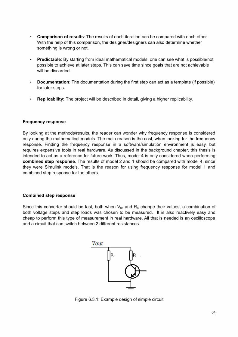
Combined step response
Since this converter should be fast, both when Vref and RC change their values, a combination ofboth voltage steps and step loads was chosen to be measured. It is also reactively easy andcheap to perform this type of measurement in real hardware. All that is needed is an oscilloscopeand a circuit that can switch between 2 different resistances.
64
Figure 6.3.1: Example design of simple circuit

Speed of system clock
The minimum clock frequency of the switch was 200 kHz, as stated in the background chapter. Toobtain functionality, a minimum system clock of 4 MHz was needed. The reason for this is theNyquist criterion. 200 kHz switching frequency needs a sample rate of 400 kHz as a minimum. A bitaccuracy of 10 bits for the ADC and DAC were chosen. Totally this results in 200 * 103 * 2 * 10 = 4MHz.
Reliability
Since all measurements were performed in a simulation environment, this thesis has highreliability. No extra noise will be added, from an unexpected source. This problem is possible, if themeasurements were performed in real hardware. If the same simulation environment is used, allthat is needed is a copy of the models. For those who wish to perform simulations in otherenvironments, the accuracy of the simulation steps (in time) shall be chosen with care. Also thealgorithms used during simulations shall preferably be the same.
Validity
One disadvantage of simulations is the validity. This is because simulations tend to be close to anideal environment. Even if there have been efforts made to avoid ideal models, one can alwaysexpect noise from unexpected sources, during hardware implementation.
65

66

7 CONCLUSIONS
7.1 Performance and complexity
In the theory chapter it is explained that slope compensation is done by modifying the controlvoltage to a ramp, instead of a constant limit. A basic solution would be to let the DAC convert aminimum of 10 voltages every switching cycle (see figure below).
In this case, it will correspond to a DAC bit rate of 40 Mbps. To obtain a good slope compensation,100 conversions would be a better choice. This will correspond to a DAC bit rate of 400 Mbps.Suppose the DAC can sample its input at either the clock edge. This would correspond to a clockfrequency of 800 MHz. These values are based on the switching frequency. For those who wish ahigher switching frequency, the requirements on the DAC will grow even more. This reminds of theprice and complexity needed to obtain a stable system, for all duty cycles using current modecontrol. Comparing this to a voltage mode converter, it is easily seen that voltage mode is apreferable choice, when price and complexity are to be reduced. This is even more clear by lookingat the boost converter. 25 bits were needed to maintain functionality. Using multipliers with a 25 bitwide bus will either take to much chip space, or take several clock cycles to calculate. But is thereany benefits using current mode control? As mentioned in the introduction chapter, current modecontrol offers better stability (see figure 7 in [14]). Current mode control implemented into FPGA:sis thus a good choice when performance and flexibility weights more than price and complexity.
67
Figure 7.1.1: Digital Slope compensation

7.2 Future work
There are totally 5 types of current mode control methods [15]. “Constant-frequency with turn-on atclock time” is the one used in this thesis. Another interesting set-up is hysteric control method (alsocurrent mode control). This type of converter does not have a fixed switching frequency. Insteadthe switching frequency depends on the rising time and falling time of the inductor current. Oneadvantage of this method is that there is no need of slope compensation. As described in thetheory chapter, the coefficients (A0, A1, B0, B1, B2) are related to the switching frequency. Using asystem with the switching frequency varying, these coefficients have to vary as well. This drawbackcan be turned into an advantage, if a fast digital system is used. Using FPGA:s, a coefficient bankcould be implemented, creating room for a more general solution. With this approach, differentvoltage levels and duty cycles could be used with the same converter. Problem statements to beanswered is given below:
• What is the relation between the amount of coefficients needed, for a certain input voltage range?
• Is it possible for the system to determine the inductor and capacitor values, without any user input?
68

69
BIBLIOGRAPHY [1] Leng Z, Liu Q, Sun J, Liu J. A research of efficiency characteristic for Buck converter. I:2010 2nd International Conference on Industrial Mechatronics and Automation (ICIMA). 2010, 232–5.
[2] Markowski P, Power Supply Control With FPGAs, HOW2POWERTODAY, April 2014, 01–4
[3] S Dhanasekaran, E.Sowdesh kumar, R.Vijaybalaji. Different Methods of Control Mode in Switch Mode Power Supply- A Comparison. International Journal of Advanced Research in Electrical, Electronics and Instrumentation Engineering (IJAREEIE) january 2014, 6718-0.
[4] Liu D, Hu A, Wang G, Hu W. Current Sharing Schemes for Multiphase Interleaved DC/DC Converter with FPGA Implementation. I: 2010 International Conference on Electrical and Control Engineering (ICECE). 2010, 3512–5.
[5] Sampath R. Digital Peak Current Mode Control of Buck Converter Using MC56F8257DSC, Freescale Semiconductor Application Report, May 2013, 08–0.
[6] Hallworth M, Shirsavar SA. Microcontroller-Based Peak Current Mode Control Using Digital Slope Compensation. IEEE Transactions on Power Electronics. Juli 2012;27(7), 3340–43.
70
[7] Poley R, Shirsavar A. Digital Peak Current Mode Control With Slope Compensation Using the TMS320F2803x, Texas Instruments Application Report April 2012, 02–3.
[8] Lee S, Practical Feedback Loop Analysis for Current-Mode Boost Converter, Texas Instruments Application Report, March 2014, 09–0.
[9] Prasuna IJ, Kavya MS, Suryanarayana K, Shrinivasa Rao BR. Digital peak current mode control of boost converter. I: 2014 Annual International Conference on Emerging Research Areas: Magnetics, Machines and Drives (AICERA/iCMMD). 2014, 1–4.
[10] Radu E, Dorin P, AN ADAPTIVE DIGITAL COMPENSATION DESIGN FOR BUCKCONVERTER TOPOLOGY, ACTA TECHNICA NAPOCENSIS Electronics and Telecommunications, 2011, 35–0
[11] Knutsson S, Digital Signalbehandling Bilinjär transform, Chalmers Lindholmen, February 1999, 01–2
[12] Ridley R, Current-Mode Control Modelling, Switching Power Magazine Designer's Series, 2006, 01–1
[13] Kondrath N, Kazimierczuk MK. Slope compensation and relative stability of peak current-mode controlled PWM dc-dc converters in CCM. I: 2013 IEEE 56th International Midwest Symposium on Circuits and Systems (MWSCAS). 2013, 477–80.
[14] Lee S, Practical Feedback Loop Analysis for Current-Mode Boost Converter, Texas Instruments Application Report, March 2014, 07–0.
[15] Timothy H, Current-Mode Control Stability Analysis For DC-DC Converters (Part 1) HOW2POWERTODAY, June 2014
71

72

APPENDIX
The following pages contain the code that describes model 4 for both buck and boost mode, inside the controller. For each block, the VHDL code is given for Boost converter followed by buck converter. This is the same code that can be found inside the simulation models. Since model 1, 2 and 3 does only contain simulink blocks, no code is given for these models.
73

------------------------------------------------------------------------------------------------------------------------------------- This block takes a digital value and gives a digital value with less amount of bits. This is becus the amount – of bits taken from DIGITAL_CONTROLLER block is more than the bits ADC can takein. Thus this block – is needed to choose out the bits that are needed to maintain functionality.------------------------------------------------------------------------------------------------------------------------------------- * INT_ BITS IS the amount of bits that represent the integer bits. -- * FRACTIONAL IS the amount of bits that represent the fractional bits.-- * DAC_BITS is the amount of bits the DAC takes in.-- * MSB_BIT_TO_DAC and LSB_TO_DAC is the MSB and LSB bits choosen out from-- * DIGITAL_CONTROLLEr block output. To know which bits to take out from the -- * DIGITAL_CONTROLLER block output, eather a simulation is needed or the -- script in matlab can be used. The script in matlab is not 100 % proven to work for any situation.
----------------------------------------------------------------------------------------------------------------------------------
library IEEE;use IEEE.STD_LOGIC_1164.all;use IEEE.numeric_std.ALL;
entity CHOOSE_BITS_BOOST is
generic (
MSB_BIT_TO_DAC: natural := 39; LSB_TO_DAC: natural := 30; INT_BITS: natural := 5;FRACTIONAL: natural := 20;DAC_BITS : natural := 10
); port ( i : in SIGNED(((2*INT_BITS + 3) + 2*FRACTIONAL - 1) downto 0);
o : out SIGNED((DAC_BITS) - 1 downto 0) ); end CHOOSE_BITS_BOOST;
architecture BEHAV of CHOOSE_BITS_BOOST isbegin
o <= i(MSB_BIT_TO_DAC downto LSB_TO_DAC);end BEHAV;
74

---------------------------------------------------------------------------------- This block takes a digital value and gives a digital value with less amount–- of bits. This is becus the amount of bits taken from DIGITAL_CONTROLLER block–- is more than the bits ADC can take in. Thus, this block is needed to choose –- out the bits that are needed to maintain functionality.---------------------------------------------------------------------------------- INT_ BITS IS the amount of bits that represent the integer bits. ---- FRACTIONAL IS the amount of bits that represent the fractional bits.
-- DAC_BITS is the amount of bits the DAC takes in.---- MSB_BIT_TO_DAC and LSB_TO_DAC is the MSB and LSB bits choosen out from-- DIGITAL_CONTROLLEr block output. To know which bits to take out from the -- DIGITAL_CONTROLLER block output, eather a simulation is needed or the script-- in matlab can be used. The script in matlab is not 100 % proven to work for-- any situation. --------------------------------------------------------------------------------
library IEEE;use IEEE.STD_LOGIC_1164.all;use IEEE.numeric_std.ALL; entity CHOOSE_BITS_BUCK is
generic (
MSB_BIT_TO_DAC : natural := 39; LSB_TO_DAC : natural := 30;
INT_BITS : natural := 5;FRACTIONAL : natural := 20;
DAC_BITS : natural := 10);
port ( i: in SIGNED(((2*INT_BITS + 3) + 2*FRACTIONAL - 1) downto 0); o: out SIGNED((DAC_BITS) - 1 downto 0)
); end CHOOSE_BITS_BUCK;
architecture BEHAV of CHOOSE_BITS_BUCK isbegin
o <= i(MSB_BIT_TO_DAC downto LSB_TO_DAC);end BEHAV;
75

------------------------------------------------------------------------------------------------------------------------------------------------------------------ This block takes a digital value that represents an error and outputs-- a Vcontrol that is supposed to represent the upper limit of the current in a-- peak current mode DC-DC buck/BOOST converter.---------------------------------------------------------------------------------- INT_ BITS IS the amount of bits that represent the integer bits. -- FRACTIONAL IS the amount of bits that represent the fractional bits.---- THE analog component values B0_VALUE, B1_VALUE, B2_VALUE, A1_VALUE, A2_VALUE –- are the coefficients that is generated by the biritcha-calculator. Since -- fractional values are used, each coefficient needs to be multiplied -- with 2^FRACTIONAL and rounded. The formulas is given below:---- B0_VALUE = round(B0*2^FRACTIONAL);-- B1_VALUE = round(B1*2^FRACTIONAL);-- B2_VALUE = round(B2*2^FRACTIONAL);-- A1_VALUE = round(A1*2^FRACTIONAL);-- A2_VALUE = round(A2*2^FRACTIONAL);------------------------------------------------------------------------------------------------------------------------------------------------------------------
library IEEE;use IEEE.STD_LOGIC_1164.all;use IEEE.numeric_std.ALL;
entity DIGITAL_CONTROLLER_BOOST is
generic(
INT_BITS : natural := 5;FRACTIONAL : natural := 20;B0_VALUE : integer := 7352;B1_VALUE : integer := 55;B2_VALUE : integer := -7298;A1_VALUE : integer := 1875184;A2_VALUE : integer := -826609
);
port (
SYSTEM_CLK : in std_logic;RESET_BLOCK : in std_logic;SAMPLE_CLK : in std_logic;E : in SIGNED((INT_BITS + FRACTIONAL - 1) downto 0);Y : out SIGNED(((2*(INT_BITS + FRACTIONAL) + 2)) downto 0)
);end DIGITAL_CONTROLLER_BOOST;
76

architecture BEHAV of DIGITAL_CONTROLLER_BOOST is
signal SAMPLE_CLK_OLD : std_logic;signal En0 : SIGNED((INT_BITS + FRACTIONAL - 1) downto 0) := (others => '0');signal En1 : SIGNED((INT_BITS + FRACTIONAL - 1) downto 0) := (others => '0');signal En2 : SIGNED((INT_BITS + FRACTIONAL - 1) downto 0) := (others => '0');signal Yn0 : SIGNED(((2*(INT_BITS+FRACTIONAL)+2))downto 0) := (others => '0');signal Yn1 : SIGNED((INT_BITS + FRACTIONAL - 1) downto 0) := (others => '0'); signal Yn2 : SIGNED((INT_BITS + FRACTIONAL - 1) downto 0) := (others => '0');signal PRECALC1 : SIGNED((2*(INT_BITS+FRACTIONAL)+1) downto 0) := (others => '0');signal PRECALC2 : SIGNED((2*(INT_BITS+FRACTIONAL)+1) downto 0) := (others => '0');
constant B0 : SIGNED((INT_BITS+FRACTIONAL-1) downto 0):=to_signed(B0_VALUE,(INT_BITS + FRACTIONAL));constant B1 : SIGNED((INT_BITS+FRACTIONAL-1) downto 0):=to_signed(B1_VALUE,(INT_BITS + FRACTIONAL));constant B2 : SIGNED((INT_BITS+FRACTIONAL-1) downto 0):=to_signed(B2_VALUE,(INT_BITS + FRACTIONAL));constant A1 : SIGNED((INT_BITS+FRACTIONAL-1) downto 0):=to_signed(A1_VALUE,(INT_BITS + FRACTIONAL));constant A2 : SIGNED((INT_BITS+FRACTIONAL-1) downto 0):=to_signed(A2_VALUE,(INT_BITS + FRACTIONAL));
beginPRECALC1 <= ((resize((Yn2*A2),PRECALC1'length) + Yn1*A1) + (resize((En1*B1),PRECALC1'length)
+ En2*B2));Yn0 <= (resize((En0*B0),Yn0'length) + PRECALC2);
Y <= Yn0;
process(SYSTEM_CLK)begin
if(rising_edge(SYSTEM_CLK)) then
if(RESET_BLOCK = '0') then
En0 <= (others => '0');En1 <= (others => '0');En2 <= (others => '0'); SAMPLE_CLK_OLD <= '0';PRECALC2 <= (others => '0');Yn1 <= (others => '0'); Yn2 <= (others => '0');
elseif((SAMPLE_CLK = '1') and (SAMPLE_CLK_OLD = '0')) then
SAMPLE_CLK_OLD <= '1';PRECALC2 <= PRECALC1;En0 <= E;
elsif((SAMPLE_CLK = '0') and (SAMPLE_CLK_OLD = '1')) then Yn2 <= Yn1;
Yn1(Yn1'length - 1) <= Yn0(Yn0'length - 1);Yn1((Yn1'length - 2) downto 0) <= Yn0(((Yn1'length – 2)+
FRACTIONAL) downto FRACTIONAL);
En2 <= En1; En1 <= En0;SAMPLE_CLK_OLD <= '0';
end if;end if;
end if;end process;
end BEHAV;
77
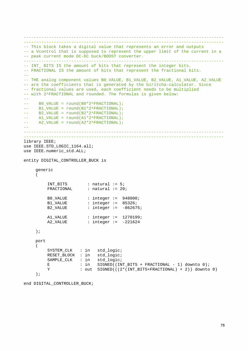
------------------------------------------------------------------------------------------------------------------------------------------------------------------ This block takes a digital value that represents an error and outputs-- a Vcontrol that is supposed to represent the upper limit of the current in a-- peak current mode DC-DC buck/BOOST converter.---------------------------------------------------------------------------------- INT_ BITS IS the amount of bits that represent the integer bits. -- FRACTIONAL IS the amount of bits that represent the fractional bits.---- THE analog component values B0_VALUE, B1_VALUE, B2_VALUE, A1_VALUE, A2_VALUE –- are the coefficients that is generated by the biritcha-calculator. Since -- fractional values are used, each coefficient needs to be multiplied -- with 2^FRACTIONAL and rounded. The formulas is given below:---- B0_VALUE = round(B0*2^FRACTIONAL);-- B1_VALUE = round(B1*2^FRACTIONAL);-- B2_VALUE = round(B2*2^FRACTIONAL);-- A1_VALUE = round(A1*2^FRACTIONAL);-- A2_VALUE = round(A2*2^FRACTIONAL);------------------------------------------------------------------------------------------------------------------------------------------------------------------library IEEE;use IEEE.STD_LOGIC_1164.all;use IEEE.numeric_std.ALL;
entity DIGITAL_CONTROLLER_BUCK is
generic(
INT_BITS : natural := 5;FRACTIONAL : natural := 20;
B0_VALUE : integer := 948000;B1_VALUE : integer := 85326;B2_VALUE : integer := -862675;
A1_VALUE : integer := 1270199;A2_VALUE : integer := -221624
);
port (
SYSTEM_CLK : in std_logic;RESET_BLOCK : in std_logic;SAMPLE_CLK : in std_logic;E : in SIGNED((INT_BITS + FRACTIONAL - 1) downto 0);Y : out SIGNED(((2*(INT_BITS+FRACTIONAL) + 2)) downto 0)
); end DIGITAL_CONTROLLER_BUCK;
78
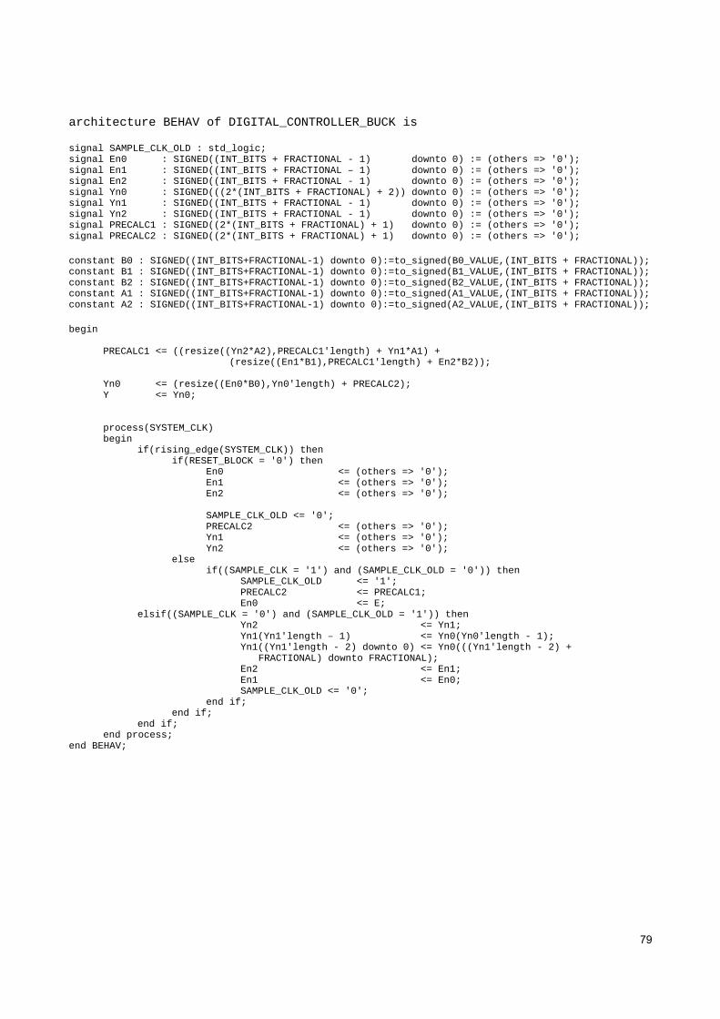
architecture BEHAV of DIGITAL_CONTROLLER_BUCK is
signal SAMPLE_CLK_OLD : std_logic;signal En0 : SIGNED((INT_BITS + FRACTIONAL - 1) downto 0) := (others => '0');signal En1 : SIGNED((INT_BITS + FRACTIONAL – 1) downto 0) := (others => '0');signal En2 : SIGNED((INT_BITS + FRACTIONAL - 1) downto 0) := (others => '0');signal Yn0 : SIGNED(((2*(INT_BITS + FRACTIONAL) + 2)) downto 0) := (others => '0');signal Yn1 : SIGNED((INT_BITS + FRACTIONAL - 1) downto 0) := (others => '0'); signal Yn2 : SIGNED((INT_BITS + FRACTIONAL - 1) downto 0) := (others => '0');signal PRECALC1 : SIGNED((2*(INT_BITS + FRACTIONAL) + 1) downto 0) := (others => '0');signal PRECALC2 : SIGNED((2*(INT_BITS + FRACTIONAL) + 1) downto 0) := (others => '0');
constant B0 : SIGNED((INT_BITS+FRACTIONAL-1) downto 0):=to_signed(B0_VALUE,(INT_BITS + FRACTIONAL));constant B1 : SIGNED((INT_BITS+FRACTIONAL-1) downto 0):=to_signed(B1_VALUE,(INT_BITS + FRACTIONAL));constant B2 : SIGNED((INT_BITS+FRACTIONAL-1) downto 0):=to_signed(B2_VALUE,(INT_BITS + FRACTIONAL));constant A1 : SIGNED((INT_BITS+FRACTIONAL-1) downto 0):=to_signed(A1_VALUE,(INT_BITS + FRACTIONAL));constant A2 : SIGNED((INT_BITS+FRACTIONAL-1) downto 0):=to_signed(A2_VALUE,(INT_BITS + FRACTIONAL));
begin
PRECALC1 <= ((resize((Yn2*A2),PRECALC1'length) + Yn1*A1) + (resize((En1*B1),PRECALC1'length) + En2*B2));
Yn0 <= (resize((En0*B0),Yn0'length) + PRECALC2);Y <= Yn0;
process(SYSTEM_CLK)begin
if(rising_edge(SYSTEM_CLK)) thenif(RESET_BLOCK = '0') then
En0 <= (others => '0');En1 <= (others => '0');En2 <= (others => '0');
SAMPLE_CLK_OLD <= '0';PRECALC2 <= (others => '0');Yn1 <= (others => '0'); Yn2 <= (others => '0');
elseif((SAMPLE_CLK = '1') and (SAMPLE_CLK_OLD = '0')) then
SAMPLE_CLK_OLD <= '1';PRECALC2 <= PRECALC1;En0 <= E;
elsif((SAMPLE_CLK = '0') and (SAMPLE_CLK_OLD = '1')) thenYn2 <= Yn1; Yn1(Yn1'length – 1) <= Yn0(Yn0'length - 1);Yn1((Yn1'length - 2) downto 0) <= Yn0(((Yn1'length - 2) +
FRACTIONAL) downto FRACTIONAL);En2 <= En1; En1 <= En0;SAMPLE_CLK_OLD <= '0';
end if; end if;
end if;end process;
end BEHAV;
79

---------------------------------------------------------------------------------- This block is a set-reset block with a leading_edge blanking protection-- against glitches in a current-mode DC-DC BUCK/BOOST converter.---------------------------------------------------------------------------------- BLANKING_WINDOW represent amount of system clock cycles to wait until RESET -- input is enabled. This will protect against gliches that occour on the RESET-- pin. The higher value BLANKING_WINDOW is set to, the longer it takes until -- RESET pin is enabled.–-- Q and Q_PRIM are outputs connected to the switches in the analog part.-- SAFE reset is an output activiating a switch, preventing the voltage to grow-- during a reset of the whole system.--------------------------------------------------------------------------------library IEEE; use IEEE.STD_LOGIC_1164.all;use IEEE.numeric_std.ALL;
entity SET_RESET_BOOST is generic (
BLANKING_WINDOW : natural := 5 ); port (
SYSTEM_CLK : in std_logic;RESET_BLOCK : in std_logic;S : in std_logic;R : in std_logic;Q : out std_logic;Q_PRIM : out std_logic;SAFE_RESET : out std_logic
); end SET_RESET_BOOST;
architecture BEHAV of SET_RESET_BOOST isbegin
process(SYSTEM_CLK)variable BLANKING_COUNTER : integer range 0 to BLANKING_WINDOW;
beginif (rising_edge(SYSTEM_CLK)) then
if(RESET_BLOCK = '0') thenBLANKING_COUNTER := 0;Q <= '0';Q_PRIM <= '0';SAFE_RESET <= '1';
elseSAFE_RESET <= '0';if(BLANKING_COUNTER < BLANKING_WINDOW) then
BLANKING_COUNTER := BLANKING_COUNTER + 1;end if;if ((R = '1')and(BLANKING_COUNTER=BLANKING_WINDOW)) then
Q <= '0';Q_PRIM <= '1';
elsif (S = '1') thenBLANKING_COUNTER := 0;Q <= '1';Q_PRIM <= '0';
end if;end if;
end if;end process;
end BEHAV;
80

---------------------------------------------------------------------------------- This block is a set-reset block with a leading_edge blanking protection-- against glitches in a current-mode DC-DC BUCK/BOOST converter.---------------------------------------------------------------------------------- BLANKING_WINDOW represent amount of system clock cycles to wait until RESET -- input is enabled. This will protect against gliches that occour on the RESET-- pin. The higher value BLANKING_WINDOW is set to, the longer it takes until -- RESET pin is enabled.---- Q and Q_PRIM are outputs connected to the switches in the analog part.-- SAFE reset is an output activiating a switch, preventing the voltage to grow-- during a reset of the whole system.--------------------------------------------------------------------------------library IEEE; use IEEE.STD_LOGIC_1164.all;use IEEE.numeric_std.ALL;
entity SET_RESET_BUCK is generic (
BLANKING_WINDOW : natural := 5 ); port (
SYSTEM_CLK : in std_logic;RESET_BLOCK : in std_logic;S : in std_logic;R : in std_logic;Q : out std_logic;Q_PRIM : out std_logic;SAFE_RESET : out std_logic
); end SET_RESET_BUCK;
architecture BEHAV of SET_RESET_BUCK isbegin
process(SYSTEM_CLK)variable BLANKING_COUNTER : integer range 0 to BLANKING_WINDOW;
beginif (rising_edge(SYSTEM_CLK)) then
if(RESET_BLOCK = '0') thenBLANKING_COUNTER := 0;Q <= '0';Q_PRIM <= '0';SAFE_RESET <= '1';
elseSAFE_RESET <= '0';if(BLANKING_COUNTER < BLANKING_WINDOW) then
BLANKING_COUNTER := BLANKING_COUNTER + 1;end if;if ((R = '1')and(BLANKING_COUNTER=BLANKING_WINDOW)) then
Q <= '0';Q_PRIM <= '1';
elsif (S = '1') thenBLANKING_COUNTER := 0;Q <= '1';Q_PRIM <= '0';
end if;end if;
end if;end process;
end BEHAV;
81

---------------------------------------------------------------------------------- * This block takes a digital value that represents Vref and outputs-- a digital value that grows towards Vref by 1 step each sampling cycle.---------------------------------------------------------------------------------- * INT_ BITS IS the amount of bits that represent the integer bits.---- * FRACTIONAL IS the amount of bits that represent the fractional bits.---- * STARTING_VALUE is the value the output begins at. This is needed for-- BOOST converter and should be the value of the input voltage to the system.---- * STEP_BITS is representing amount of fractional bits needed for each step.-- The more bits, the smaller step. For example:-- ** 2 bits => a step is 2^-2-- ** 4 bits => a step is 2^-4-- ** 8 bits => a step is 2^-8-- ** n bits => a step is 2^-n---------------------------------------------------------------------------------- ====== **** OBS: ADC_BITS < STEP_BITS < FRACTIONAL **** ======-- =========================================================-- STEP_BITS should not be too high or too low. -- In both cases, it can lead to instability.-- =========================================================--------------------------------------------------------------------------------
library IEEE;use IEEE.STD_LOGIC_1164.all;use IEEE.numeric_std.ALL;
entity SOFT_START_BOOST isgeneric(
-- THis is needed for the BOOST ONVERTER.-- The start value should be more than-- Vin on the converter input.START_VALUE : natural := 5;STEP_BITS_UP : natural := 7;STEP_BITS_DOWN : natural := 10;INT_BITS : natural := 5;FRACTIONAL : natural := 20
);
port (
SYSTEM_CLK : in std_logic;RESET_BLOCK : in std_logic;SAMPLE_CLK : in std_logic;Vref_in : in SIGNED((INT_BITS + FRACTIONAL - 1) downto 0);Vref_out : buffer SIGNED(24 downto 0)
) end SOFT_START_BOOST;
82

architecture BEHAV of SOFT_START_BOOST is
type UP_OR_DOWN is (UP, DOWN); signal SAMPLE_CLK_OLD : std_logic;signal DIRECTION : UP_OR_DOWN := UP_OR_DOWN'(UP);
signal Old_Vref : SIGNED((INT_BITS + FRACTIONAL - 1) downto 0) := (others => '0');signal Soft_Vref1 : SIGNED((INT_BITS + FRACTIONAL - 1) downto 0) := (others => '0');signal Soft_Vref2 : SIGNED((INT_BITS + FRACTIONAL - 1) downto 0) := (others => '0');
constant STARTING_VALUE : SIGNED((INT_BITS + FRACTIONAL - 1) downto 0) := to_signed(START_VALUE*(2**FRACTIONAL),(INT_BITS + FRACTIONAL));
constant STEP_UP : SIGNED((INT_BITS + FRACTIONAL - 1) downto 0) := to_signed(2**(FRACTIONAL - STEP_BITS_UP),(INT_BITS + FRACTIONAL));
constant STEP_DOWN : SIGNED((INT_BITS + FRACTIONAL - 1) downto 0) := to_signed(2**(FRACTIONAL - STEP_BITS_DOWN),(INT_BITS + FRACTIONAL));
beginvref_out <= Soft_Vref2 + STARTING_VALUE; process(SYSTEM_CLK)begin
if(rising_edge(SYSTEM_CLK)) thenif(RESET_BLOCK = '0') then
DIRECTION <= UP;SAMPLE_CLK_OLD <= '0';Old_Vref <= (others => '0');Soft_Vref1 <= (others => '0');Soft_Vref2 <= (others => '0');
else if((SAMPLE_CLK = '1') and (SAMPLE_CLK_OLD = '0')) then
SAMPLE_CLK_OLD <= '1';-- Depending on direction, change the value of Vref-- by adding a step value each sample cycle.if(DIRECTION = UP) then
if(Vref_out < Vref_in) thenSoft_Vref2 <= (Soft_Vref1 + STEP_UP);
end if;elsif(DIRECTION = DOWN) then
if(Vref_out > Vref_in) thenSoft_Vref2 <= (Soft_Vref1 - STEP_DOWN);
end if;end if;
-- If Vref changed, change direction if needed.if(Vref_in > Old_Vref) then
DIRECTION <= UP;Old_Vref <= Vref_in;
elsif(Vref_in < Old_Vref) thenDIRECTION <= DOWN;Old_Vref <= Vref_in;
end if;
elsif((SAMPLE_CLK = '0') and (SAMPLE_CLK_OLD = '1')) thenSAMPLE_CLK_OLD <= '0';Soft_Vref1 <= Soft_Vref2;
end if;end if;
end if; end process;
end BEHAV;
83
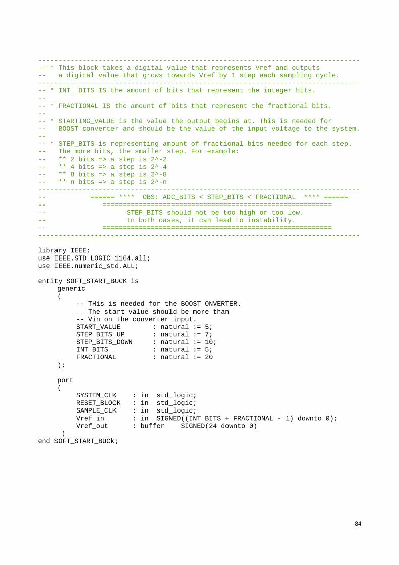
---------------------------------------------------------------------------------- * This block takes a digital value that represents Vref and outputs-- a digital value that grows towards Vref by 1 step each sampling cycle.---------------------------------------------------------------------------------- * INT_ BITS IS the amount of bits that represent the integer bits.---- * FRACTIONAL IS the amount of bits that represent the fractional bits.---- * STARTING_VALUE is the value the output begins at. This is needed for-- BOOST converter and should be the value of the input voltage to the system.---- * STEP_BITS is representing amount of fractional bits needed for each step.-- The more bits, the smaller step. For example:-- ** 2 bits => a step is 2^-2-- ** 4 bits => a step is 2^-4-- ** 8 bits => a step is 2^-8-- ** n bits => a step is 2^-n---------------------------------------------------------------------------------- ====== **** OBS: ADC_BITS < STEP_BITS < FRACTIONAL **** ======-- =========================================================-- STEP_BITS should not be too high or too low. -- In both cases, it can lead to instability.-- =========================================================--------------------------------------------------------------------------------
library IEEE;use IEEE.STD_LOGIC_1164.all;use IEEE.numeric_std.ALL;
entity SOFT_START_BUCK isgeneric(
-- THis is needed for the BOOST ONVERTER.-- The start value should be more than-- Vin on the converter input.START_VALUE : natural := 5;STEP_BITS_UP : natural := 7;STEP_BITS_DOWN : natural := 10;INT_BITS : natural := 5;FRACTIONAL : natural := 20
);
port (
SYSTEM_CLK : in std_logic;RESET_BLOCK : in std_logic;SAMPLE_CLK : in std_logic;Vref_in : in SIGNED((INT_BITS + FRACTIONAL - 1) downto 0);Vref_out : buffer SIGNED(24 downto 0)
) end SOFT_START_BUCk;
84
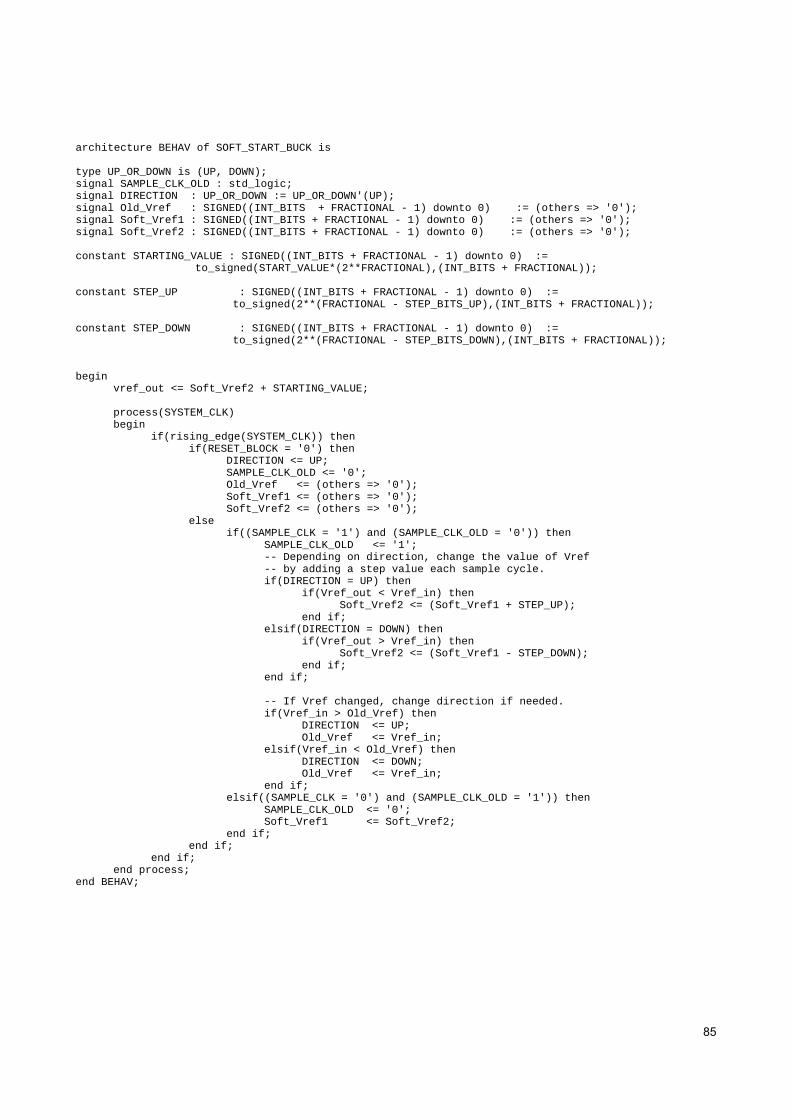
architecture BEHAV of SOFT_START_BUCK is
type UP_OR_DOWN is (UP, DOWN);signal SAMPLE_CLK_OLD : std_logic;signal DIRECTION : UP_OR_DOWN := UP_OR_DOWN'(UP);signal Old_Vref : SIGNED((INT_BITS + FRACTIONAL - 1) downto 0) := (others => '0');signal Soft_Vref1 : SIGNED((INT_BITS + FRACTIONAL - 1) downto 0) := (others => '0');signal Soft_Vref2 : SIGNED((INT_BITS + FRACTIONAL - 1) downto 0) := (others => '0');
constant STARTING_VALUE : SIGNED((INT_BITS + FRACTIONAL - 1) downto 0) := to_signed(START_VALUE*(2**FRACTIONAL),(INT_BITS + FRACTIONAL));
constant STEP_UP : SIGNED((INT_BITS + FRACTIONAL - 1) downto 0) := to_signed(2**(FRACTIONAL - STEP_BITS_UP),(INT_BITS + FRACTIONAL));
constant STEP_DOWN : SIGNED((INT_BITS + FRACTIONAL - 1) downto 0) :=
to_signed(2**(FRACTIONAL - STEP_BITS_DOWN),(INT_BITS + FRACTIONAL));
beginvref_out <= Soft_Vref2 + STARTING_VALUE;
process(SYSTEM_CLK)begin
if(rising_edge(SYSTEM_CLK)) thenif(RESET_BLOCK = '0') then
DIRECTION <= UP;SAMPLE_CLK_OLD <= '0';Old_Vref <= (others => '0');Soft_Vref1 <= (others => '0');Soft_Vref2 <= (others => '0');
else if((SAMPLE_CLK = '1') and (SAMPLE_CLK_OLD = '0')) then
SAMPLE_CLK_OLD <= '1';-- Depending on direction, change the value of Vref-- by adding a step value each sample cycle.if(DIRECTION = UP) then
if(Vref_out < Vref_in) thenSoft_Vref2 <= (Soft_Vref1 + STEP_UP);
end if;elsif(DIRECTION = DOWN) then
if(Vref_out > Vref_in) thenSoft_Vref2 <= (Soft_Vref1 - STEP_DOWN);
end if;end if;
-- If Vref changed, change direction if needed.if(Vref_in > Old_Vref) then
DIRECTION <= UP;Old_Vref <= Vref_in;
elsif(Vref_in < Old_Vref) thenDIRECTION <= DOWN;Old_Vref <= Vref_in;
end if;elsif((SAMPLE_CLK = '0') and (SAMPLE_CLK_OLD = '1')) then
SAMPLE_CLK_OLD <= '0';Soft_Vref1 <= Soft_Vref2;
end if;end if;
end if; end process;
end BEHAV;
85

--------------------------------------------------------------------------------
-- * This block takes 2 inputs (a connects to SOFT_START block and-- b connects to VOLTAGE_DIVIDER block), and performs a subtraction.---------------------------------------------------------------------------------- * INT_ BITS IS the amount of bits that represent the integer bits. ---- * FRACTIONAL IS the amount of bits that represent the fractional bits.--------------------------------------------------------------------------------
library ieee;use ieee.std_logic_1164.all;use ieee.numeric_std.all;
entity SUBTRACTOR_BOOST is
generic(
INT_BITS : natural := 5;FRACTIONAL : natural := 20
);
port (
a : in SIGNED((INT_BITS + FRACTIONAL - 1) downto 0);b : in SIGNED((INT_BITS + FRACTIONAL - 1) downto 0);result : out SIGNED((INT_BITS + FRACTIONAL - 1) downto 0)
);end entity;
architecture behav of SUBTRACTOR_BOOST isbegin
process(a,b)begin
result <= a - b;end process;
end behav;
86

---------------------------------------------------------------------------------- * This block takes 2 inputs (a connects to SOFT_START block and-- b connects to VOLTAGE_DIVIDER block), and performs a subtraction.---------------------------------------------------------------------------------- * INT_ BITS IS the amount of bits that represent the integer bits. ---- * FRACTIONAL IS the amount of bits that represent the fractional bits.--------------------------------------------------------------------------------
library ieee;use ieee.std_logic_1164.all;use ieee.numeric_std.all;
entity SUBTRACTOR_BUCK is
generic(
INT_BITS : natural := 5;FRACTIONAL : natural := 20
);
port (
a : in SIGNED((INT_BITS + FRACTIONAL - 1) downto 0);b : in SIGNED((INT_BITS + FRACTIONAL - 1) downto 0);result : out SIGNED((INT_BITS + FRACTIONAL - 1) downto 0)
);end entity;
architecture behav of SUBTRACTOR_BUCK isbegin
process(a,b)begin
result <= a - b;end process;
end behav;
87

---------------------------------------------------------------------------------- * This block takes a digital value form the ADC and outputs a -- digital value to the rest of the system.---------------------------------------------------------------------------------- * ADC BITS IS the amount of bits the ADC gives to the FPGA.-- -- * INT_ BITS IS the amount of bits that represent the integer bits.---- * FRACTIONAL IS the amount of bits that represent the fractional bits.---- * Since the output voltage is divided with a resistive divider outside -- the FPGA, one need to multiply back with this value inside the FPGA, -- This is the "DIVIDER_VALUE"---- * since the ADC output represents a fractional value of its Vref,-- one need to multiply the digital value with the Vref.---- * Also, the DIVIDER_VALUE needs to be multiplied WITH 2^FRACTIONAL where-- FRACTIONAL is fractional bits used.
-- * the formula is: DIVIDER_VALUE = round(Vref_ADC*DIVIDER_GAIN*2^FRACTIONAL)-- where:-- ** DIVIDER_GAIN is the value the resisitive divider outside the FPGA-- divides the voltage with. -- ** Vref_ADC is the reference voltage to the ADC.-- ** FRACTIONAL is the amount of bits that represent the fractional values -- --------------------------------------------------------------------------------
library IEEE;use IEEE.STD_LOGIC_1164.all;use IEEE.numeric_std.ALL;
entity VOLTAGE_DIVIDER_BOOST is
generic (
ADC_BITS : natural := 10;INT_BITS : natural := 5; FRACTIONAL : natural := 20;
-- ADC maximal voltage = 3 (V).-- Voltage divider gain = 5/3.-- (5/3)*3*(2^FRACTIONAL) = 15728640 DIVIDER_VALUE : natural := 15728640--5242880 );
port (
SYSTEM_CLK : in std_logic;RESET_BLOCK : in std_logic;ADC : in UNSIGNED((ADC_BITS - 1) downto 0);Y : out SIGNED((INT_BITS + FRACTIONAL - 1) downto 0)
);end VOLTAGE_DIVIDER_BOOST;
88
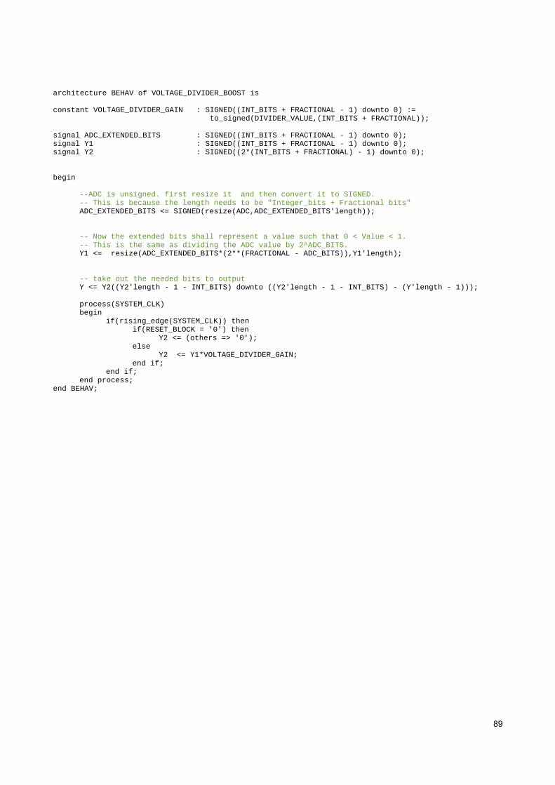
architecture BEHAV of VOLTAGE_DIVIDER_BOOST is constant VOLTAGE_DIVIDER_GAIN : SIGNED((INT_BITS + FRACTIONAL - 1) downto 0) := to_signed(DIVIDER_VALUE,(INT_BITS + FRACTIONAL));
signal ADC_EXTENDED_BITS : SIGNED((INT_BITS + FRACTIONAL - 1) downto 0);signal Y1 : SIGNED((INT_BITS + FRACTIONAL - 1) downto 0);signal Y2 : SIGNED((2*(INT_BITS + FRACTIONAL) - 1) downto 0);
begin --ADC is unsigned. first resize it and then convert it to SIGNED.-- This is because the length needs to be "Integer_bits + Fractional bits"ADC_EXTENDED_BITS <= SIGNED(resize(ADC,ADC_EXTENDED_BITS'length));
-- Now the extended bits shall represent a value such that 0 < Value < 1.-- This is the same as dividing the ADC value by 2^ADC_BITS.Y1 <= resize(ADC_EXTENDED_BITS*(2**(FRACTIONAL - ADC_BITS)),Y1'length);
-- take out the needed bits to outputY <= Y2((Y2'length - 1 - INT_BITS) downto ((Y2'length - 1 - INT_BITS) - (Y'length - 1)));
process(SYSTEM_CLK)begin
if(rising_edge(SYSTEM_CLK)) thenif(RESET_BLOCK = '0') then
Y2 <= (others => '0');else
Y2 <= Y1*VOLTAGE_DIVIDER_GAIN; end if;
end if;end process;
end BEHAV;
89

---------------------------------------------------------------------------------- * This block takes a digital value form the ADC and outputs a -- digital value to the rest of the system.---------------------------------------------------------------------------------- * ADC BITS IS the amount of bits the ADC gives to the FPGA.-- -- * INT_ BITS IS the amount of bits that represent the integer bits.---- * FRACTIONAL IS the amount of bits that represent the fractional bits.---- * Since one divided the output voltage with a resistive divider outside -- the FPGA, this value needs to be multiplied back inside the FPGA. -- This is the "DIVIDER_VALUE"---- * since the ADC output represents a fractional value of its Vref,-- the digital value needs to be multiplied with the Vref.---- * Also, one need to multiply the DIVIDER_VALUE WITH 2^FRACTIONAL where-- FRACTIONAL is the fractional bits.
-- * the formula is: DIVIDER_VALUE = round(Vref_ADC*DIVIDER_GAIN*2^FRACTIONAL)-- where:-- ** DIVIDER_GAIN is the value the resisitive divider outside the FPGA-- divides the voltage with. -- ** Vref_ADC is the reference voltage to the ADC.-- ** FRACTIONAL is the amount of bits that represent the fractional values. -- --------------------------------------------------------------------------------
library IEEE;use IEEE.STD_LOGIC_1164.all;use IEEE.numeric_std.ALL;
entity VOLTAGE_DIVIDER_BUCK is
generic (
ADC_BITS : natural := 10; INT_BITS : natural := 5; FRACTIONAL : natural := 20;
-- ADC maximal voltage = 3 (V).-- Voltage divider gain = 5/3.-- (5/3)*3*(2^FRACTIONAL) = 15728640 DIVIDER_VALUE b : natural := 5242880
);port (
SYSTEM_CLK : in std_logic;RESET_BLOCK : in std_logic;ADC : in UNSIGNED((ADC_BITS - 1) downto 0);Y : out SIGNED((INT_BITS + FRACTIONAL - 1) downto 0)
);
end VOLTAGE_DIVIDER_BUCK;
90

architecture BEHAV of VOLTAGE_DIVIDER_BUCK is constant VOLTAGE_DIVIDER_GAIN : SIGNED((INT_BITS + FRACTIONAL - 1) downto 0) := to_signed(DIVIDER_VALUE,(INT_BITS + FRACTIONAL));
signal ADC_EXTENDED_BITS : SIGNED((INT_BITS + FRACTIONAL - 1) downto 0);
signal Y1 :SIGNED((INT_BITS + FRACTIONAL - 1) downto 0);signal Y2 :SIGNED((2*(INT_BITS + FRACTIONAL) - 1) downto 0);
begin
--ADC is unsigned. So resize it first and then convert it to SIGNED.-- This is because one want the length to be "Integer_bits + Fractional bits"ADC_EXTENDED_BITS <= SIGNED(resize(ADC,ADC_EXTENDED_BITS'length));
-- Now the extended bits needs to represent a value such that 0 < Value < 1.-- This is the same as dividing the ADC value by 2^ADC_BITS.Y1 <= resize(ADC_EXTENDED_BITS*(2**(FRACTIONAL - ADC_BITS)),Y1'length);
-- take out the needed bits to outputY <= Y2((Y2'length - 1 - INT_BITS) downto ((Y2'length - 1 - INT_BITS) - (Y'length - 1)));
process(SYSTEM_CLK)begin
if(rising_edge(SYSTEM_CLK)) thenif(RESET_BLOCK = '0') then
Y2 <= (others => '0');else
Y2 <= Y1*VOLTAGE_DIVIDER_GAIN; end if;
end if;end process;
end BEHAV;
91

Institutionen för systemteknikDepartment of Electrical Engineering